Embed Size (px)
Citation preview

Motion Control Card / IC
MC8041A / MCX314User’s Manual
MC8041A / MCX314User’s Manual
Ver 2.0
P L E N T Y I S L A N D ( T A I W A N ) C O R P O R A T I O N

MC8041A
1
Contents1. Introduct ion . . . . . . . . . . . . . . . . . . . . . . . . . . . . . . . . . . . . . . . . . . . . . . . . . . . . . . . . . . . . . . . . . . . . . . . . . . . . . . . . . . . . . . . . . . . . . . . . . . . . . . . . . . . . . . 0
2. I /O Address Sett ing and Read / Write Register. . . . . . . . . . . . . . . . . . . . . . . . . . . . . . . . . . . . . . . . . . . . . . . . . . . . . . . . . . . . . . 1
3. I /O Interfaces . . . . . . . . . . . . . . . . . . . . . . . . . . . . . . . . . . . . . . . . . . . . . . . . . . . . . . . . . . . . . . . . . . . . . . . . . . . . . . . . . . . . . . . . . . . . . . . . . . . . . . . . . . . 2
3.1. Descript ions of ISA BUS Signals . . . . . . . . . . . . . . . . . . . . . . . . . . . . . . . . . . . . . . . . . . . . . . . . . . . . . . . . . . . . . . . . . . . . . . . . . . . 23.2. Pin Def ini t ion of I /O Connector . . . . . . . . . . . . . . . . . . . . . . . . . . . . . . . . . . . . . . . . . . . . . . . . . . . . . . . . . . . . . . . . . . . . . . . . . . . . . 33.3. Drive Pulse Signal (nP+P, nP+N, nP-P, nP-N) . . . . . . . . . . . . . . . . . . . . . . . . . . . . . . . . . . . . . . . . . . . . . . . . . . . . . . . . . 53.4. General Purpose Output Signal (nOUT7 ~ nOUT4) . . . . . . . . . . . . . . . . . . . . . . . . . . . . . . . . . . . . . . . . . . . . . . . . . . . 63.5. Over Limit Signal (nLMT+, nLMT-) . . . . . . . . . . . . . . . . . . . . . . . . . . . . . . . . . . . . . . . . . . . . . . . . . . . . . . . . . . . . . . . . . . . . . . . . . 63.6. Decelerat ing / Sudden Stop Input Signal (nIN1, nIN2, nIN3) . . . . . . . . . . . . . . . . . . . . . . . . . . . . . . . . . . . . . . 73.7. Input Signal for Servo Driver (nINPOS, nALARM) .. . . . . . . . . . . . . . . . . . . . . . . . . . . . . . . . . . . . . . . . . . . . . . . . . . 73.8. Encoder Input Signal (nECAP, nECAN, nECBP, nECBN, nIN0P, nIN0N) . . . . . . . . . . . . . . . . . . . . . . 83.9. External Driv ing Control Input Signal (nEX0P+, nEX0P-) . . . . . . . . . . . . . . . . . . . . . . . . . . . . . . . . . . . . . . . . . . 93.10 Emergency Stop Input Signal(EMG) . . . . . . . . . . . . . . . . . . . . . . . . . . . . . . . . . . . . . . . . . . . . . . . . . . . . . . . . . . . . . . . . . . . . 103.11 External Power Input (VEX) . . . . . . . . . . . . . . . . . . . . . . . . . . . . . . . . . . . . . . . . . . . . . . . . . . . . . . . . . . . . . . . . . . . . . . . . . . . . . . . . 10
4. Interrupt Sett ing. . . . . . . . . . . . . . . . . . . . . . . . . . . . . . . . . . . . . . . . . . . . . . . . . . . . . . . . . . . . . . . . . . . . . . . . . . . . . . . . . . . . . . . . . . . . . . . . . . . . . . 11
5. Connect ion Examples for Motor Drivers . . . . . . . . . . . . . . . . . . . . . . . . . . . . . . . . . . . . . . . . . . . . . . . . . . . . . . . . . . . . . . . . . . . . . 12
5.2 Connect ion with Pulse-type Servo Motor Drives . . . . . . . . . . . . . . . . . . . . . . . . . . . . . . . . . . . . . . . . . . . . . . . . . . . . . . 13
6. I /O Signal Timing . . . . . . . . . . . . . . . . . . . . . . . . . . . . . . . . . . . . . . . . . . . . . . . . . . . . . . . . . . . . . . . . . . . . . . . . . . . . . . . . . . . . . . . . . . . . . . . . . . . . 14
6.2 Indiv idual Dr iv ing . . . . . . . . . . . . . . . . . . . . . . . . . . . . . . . . . . . . . . . . . . . . . . . . . . . . . . . . . . . . . . . . . . . . . . . . . . . . . . . . . . . . . . . . . . . . . . . 146.3 Interpolat ion Driv ing . . . . . . . . . . . . . . . . . . . . . . . . . . . . . . . . . . . . . . . . . . . . . . . . . . . . . . . . . . . . . . . . . . . . . . . . . . . . . . . . . . . . . . . . . . . 146.4 Input Pulse Timing. . . . . . . . . . . . . . . . . . . . . . . . . . . . . . . . . . . . . . . . . . . . . . . . . . . . . . . . . . . . . . . . . . . . . . . . . . . . . . . . . . . . . . . . . . . . . . 156.5 Sudden Stop Timing. . . . . . . . . . . . . . . . . . . . . . . . . . . . . . . . . . . . . . . . . . . . . . . . . . . . . . . . . . . . . . . . . . . . . . . . . . . . . . . . . . . . . . . . . . . . 166.6 Decelerat ing Stop Timing . . . . . . . . . . . . . . . . . . . . . . . . . . . . . . . . . . . . . . . . . . . . . . . . . . . . . . . . . . . . . . . . . . . . . . . . . . . . . . . . . . . . 16
7. Jumper and Switch Layout . . . . . . . . . . . . . . . . . . . . . . . . . . . . . . . . . . . . . . . . . . . . . . . . . . . . . . . . . . . . . . . . . . . . . . . . . . . . . . . . . . . . . . . . 17
8. Specif icat ions . . . . . . . . . . . . . . . . . . . . . . . . . . . . . . . . . . . . . . . . . . . . . . . . . . . . . . . . . . . . . . . . . . . . . . . . . . . . . . . . . . . . . . . . . . . . . . . . . . . . . . . . . 18

1. Introduction
MC8041A is a high-speed 4-axis PC-Based motion control card for stepper or pulse-type servo motor drivers.Its features are:
. 4-axis independent position / speed control for stepper / pulse-type servo motor drivers
. Linear interpolation for any 2 or 3 axes
. Circular interpolation for any 2 axes
. Bit pattern interpolation for any 2 or 3 axesMC8041A, equipped with our 4-axis motion control IC MCX314, can be directly connect to the ISA busexpansion slot on PCs and their compatible machines.
The following is the functional blocks of MC8401A including MCX314, ISA BUS interface and each I/Ointerface. Please refer MCX314 manual for the functions in details.
(X axis I/O interface)
MCX314
Line driver26LS31
Output buffer74LS06
Photo coupler &RC filter
High-speed photocoupler
XP+P/NXP-P/N
XOUT7~4
XLMT+XLMT-XIN3~1XINPOSXALARM
XECAP/NXECBP/NXINPO/N
Pulse output
General output
Encoder signal input
+Limit input
Deceleration inputServo motor signal
Y Axis Interfaceidentical to the Input / Output interface of X-axis
EMG Emergency stop
ISABUS
Z Axis Interfaceidentical to the Input / Output interface of X-axis
U Axis Interfaceidentical to the Input / Output interface of X-axis
-Limit input
Servo alarm
Photo coupler&
RC filter
XEXOP+XEXOP-
+ Dir. jog-Dir. jog
VEX External power(DC12~24V)
XP+P/NXP-P/N
XOUT7~4
XLMTMXIN3~1XINPOSXALARM
XECAXECBXINPO
XEXOP+XEXOP-
XLMTP
CLK
RESETN
CSN
EMGNPhoto coupler
&RC filter
Crystal oscillator16MHz
Addressdecoder
A2~0WRNRDN
RESETDRV
I/O add.setting switch
Bi-directionbuffer
Buffer
IRQ3IRQ4IRQ5IRQ6IRQ7
IRQ10IRQ11IRQ12IRQ14IRQ15
AEN
SA15~4
IOCS16*
SA3~1IOW*IOR*
SD15~0
Functional Blocks of MC8041A

MCX314
1
2. I/O Address Setting and Read / Write Register
I/O Address SettingThe I/O port address of MCX314 includes the higher 12 bits, SA15~SA4, of ISA bus I/O address SA15~SA0.This address is set by SW1 and SW2 slide dip switches. The lower 3 bits, SA3~SA1, are used for IC internalread / write register codes.
The slide dip switches SW1 and SW2 are with ON and OFF level for SA15 ~ SA4. Switch “ON” to set abinary value 0; switch “OFF” to set a binary value 1 (see the graph below).
1 2 3 1 2 3 4 5 6 7 8
ONONSW2 SW1
ON : 0OFF:1
4
the setting of I/O address 0280~028Fh
This graph shows the initial setting of 0280~028Fh. The user should pay attention not to overlap setting thisaddress with the address of PC main board and / or other I/O cards.
Read / Write RegisterThe table below lists the I/O mapped read/write registers of MC8041A. All of the registers are accessed by 16-bit format. The inside number of ( ) shows the register address when 0280~028Fh of SW1 and SW2 are set.The address setting needs to use word-access, not byte-access. Please refer to Chapter 4 of MCX314 manualfor register setting..
I/O Address Write Register Read RegisterSA3 SA2 SA1 Symbol Register Name Symbol Register Name
0 0 0(0280h)
WR0 Command Register RR0 Main status register
0 0 1
(0282h)
XWR1Y WR1Z WR1U WR1
X axis mode register 1Y axis mode register 1Z axis mode register 1U axis mode register 1
XRR1YRR1ZRR1URR1
X axis status register 1Y axis status register 1Z axis status register 1U axis status register 1
0 1 0 XWR2Y WR2Z WR2U WR2
X axis mode register 2Y axis mode register 2Z axis mode register 2U axis mode register 2
(0284h)
BP1P BP1P register
XRR2YRR2ZRR2URR2
X axis status register 2Y axis status register 2Z axis status register 2U axis status register 2
0 1 1 XWR3Y WR3Z WR3U WR3
X axis mode register 3Y axis mode register 3Z axis mode register 3U axis mode register 3
(0286h)
BP1M BP1M register
XRR3YRR3ZRR3URR3
X axis status register 3Y axis status register 3Z axis status register 3U axis status register 3
1 0 0 WR4 Output register(0288h) BP2P BP2P register
RR4 Input register 1
1 0 1 WR5 Interpolation mode register(028Ah) BP2M BP2M register
RR5 Input register 2
1 1 0 WR6 Data writing register 1(028Ch) BP3P BP3P register
RR6 Data reading register 1
1 1 1 WR7 Data writing register 2(028Eh) BP3M BP3M register
RR7 Data reading register 2

MCX314
2
3. I/O InterfacesThis chapter describes connector I/O signals. The standard ISA bus is used as the board edge connector.Here, the signal introduction just focuses on the pins used for MX8041A. nOOOO represents any one of X, Y,Z and U axes.
3.1. Descriptions of ISA BUS Signals
Pin Signal Name Descriptions I/O Pin Signal Name Descriptions I/OA1 B1 GND GroundA2 SD7 Data I/O B2 RESTDRV Reset Signal InputA3 SD6 Data I/O B3 + 5V PowerA4 SD5 Data I/O B4A5 SD4 Data I/O B5A6 SD3 Data I/O B6A7 SD2 Data I/O B7A8 SD1 Data I/O B8A9 SD0 Data I/O B9
A10 B10 GND GroundA11 AEN Address Enable Input B11A12 B12A13 B13 IOW I/O Write InputA14 B14 IOR I/O Read InputA15 B15A16 SA15 Address Input B16A17 SA14 Address Input B17A18 SA13 Address Input B18A19 SA12 Address Input B19A20 SA11 Address Input B20A21 SA10 Address Input B21 IRQ7 Interrupt Request Signal OutputA22 SA9 Address Input B22 IRQ6 Interrupt Request Signal OutputA23 SA8 Address Input B23 IRQ5 Interrupt Request Signal OutputA24 SA7 Address Input B24 IRQ4 Interrupt Request Signal OutputA25 SA6 Address Input B25 IRQ3 Interrupt Request Signal OutputA26 SA5 Address Input B26A27 SA4 Address Input B27A28 SA3 Address Input B28A29 SA2 Address Input B29 + 5V PowerA30 SA1 Address Input B30A31 SA0 Address Input B31 GND GroundC1 D1C2 D2 IOCS16 16 bits I/O repeating signal OutputC3 D3 IRQ10 Interrupt Request Signal OutputC4 D4 IRQ11 Interrupt Request Signal OutputC5 D5 IRQ12 Interrupt Request Signal OutputC6 D6 IRQ15 Interrupt Request Signal OutputC7 D7 IRQ14 Interrupt Request Signal OutputC8 D8C9 D9
C10 D10C11 SD8 Data I/O D11C12 SD9 Data I/O D12C13 SD10 Data I/O D13C14 SD11 Data I/O D14C15 SD12 Data I/O D15C16 SD13 Data I/O D16 + 5V PowerC17 SD14 Data I/O D17C18 SD15 Data I/O D18 GND Ground

MCX314
3
3.2. Pin Definition of I/O Connector
See the diagram below: when the first pin (¡ ¶) is found, the upper cable, from right (red wire) to left are thepins A1, A2, A3, …, A49, A50, and lower cable from right (red wire) to left are the pins B2, B3, …, B49, B50.Connector type: board side.. FX2B-100P -1.27DS(HIROSE)
cable side.. FX2B-100S -1.27R(HIROSE)
A50 A49 • • • • • • • • • • • • • A2 A1
B50 B49 • • • • • • • • • • • • • B2 B1
B50 B49 B2 B1
A2 A1A50 A49
I/O Connector
1st Pin
Pin Signal Name I/O Contents Pin Signal Name I/O Contents
A1 VEX Input External Power(DC12~24V) B1 VEX Input External Power (DC12~24V)
A2 EMG Input Emergency Stop (for all axes) B2
A3 XLMT+ Input + Direction Limit of X axis B3 ZLMT+ Input + Direction Limit of Z axis
A4 XLMT- Input - Direction Limit of X axis B4 ZLMT- Input - Direction Limit of Z axis
A5 XIN1 Input Decelerating / Sudden Stop of X axis B5 ZIN1 Input Decelerating / Sudden Stop of Z axis
A6 XIN2 Input Decelerating / Sudden Stop of X axis B6 ZIN2 Input Decelerating / Sudden Stop of Z axis
A7 XIN3 Input Decelerating / Sudden Stop of X axis B7 ZIN3 Input Decelerating / Sudden Stop of Z axis
A8 YLMT+ Input + Direction Limit of Y axis B8 ULMT+ Input + Direction Limit of U axis
A9 YLMT- Input - Direction Limit of Y axis B9 ULMT- Input - Direction Limit of U axis
A10 YIN1 Input Decelerating / Sudden Stop of Y axis B10 UIN1 Input Decelerating / Sudden Stop of U axis
A11 YIN2 Input Decelerating / Sudden Stop of Y axis B11 UIN2 Input Decelerating / Sudden Stop of U axis
A12 YIN3 Input Decelerating / Sudden Stop of Y axis B12 UIN3 Input Decelerating / Sudden Stop of U axis
A13 XINPOS Input Servo In-positioning of X axis B13 ZINPOS Input Servo In-positioning of Z axis
A14 XALARM Input Servo Error of X axis B14 ZALARM Input Servo Error of Z axis
A15 XECAP Input Encoder Phase A of X axis B15 ZECAP Input Encoder Phase A of Z axis
A16 XECAN Input Encoder Phase A of X axis B16 ZECAN Input Encoder Phase A of Z axis
A17 XECBP Input Encoder Phase B of X axis B17 ZECBP Input Encoder Phase B of Z axis
A18 XECBN Input Encoder Phase B of X axis B18 ZECBN Input Encoder Phase B of Z axis
A19 XIN0P Input Encoder Phase Z of X axis B19 ZIN0P Input Encoder Phase Z of Z axis
A20 XIN0N Input Encoder Phase Z of X axis B20 ZIN0N Input Encoder Phase Z of Z axis
A21 YINPOS Input Servo In-positioning of Y axis B21 UINPOS Input In-positioning of U axis
A22 YALARM Input Servo Error of Y axis B22 UALARM Input Servo Error of U axis
A23 YECAP Input Encoder Phase A of Y axis B23 UECAP Input Encoder Phase A of U axis
A24 YECAN Input Encoder Phase A of Y axis B24 UECAN Input Encoder Phase A of U axis
A25 YECBP Input Encoder Phase B of Y axis B25 UECBP Input Encoder Phase B of U axis
A26 YECBN Input Encoder Phase B of Y axis B26 UECBN Input Encoder Phase B of U axis
A27 YIN0P Input Encoder Phase Z of Y axis B27 UIN0P Input Encoder Phase Z of U axis
A28 YIN0N Input Encoder Phase Z of Y axis B28 UIN0N Input Encoder Phase Z of U axis
A29 XEXOP+ Input + Direction Drive Operation of X axis B29 ZEXOP+ Input + Direction Drive Operation of Z axis
A30 XEXOP- Input – Direction Drive Operation of X axis B30 ZEXOP- Input – Direction Drive Operation of Z axis
A31 YEXOP+ Input + Direction Drive Operation of Y axis B31 UEXOP+ Input + Direction Drive Operation of U axis
A32 YEXOP- Input – Direction Drive Operation of Y axis B32 UEXOP- Input – Direction Drive Operation of U axis
A33 GND Ground B33 GND Ground
A34 XOUT4 Output General Purpose Output of X axis B34 ZOUT4 Output General Purpose Output of Z axis
A35 XOUT5 Output General Purpose Output of X axis B35 ZOUT5 Output General Purpose Output of Z axis
A36 XOUT6 Output General Purpose Output of X axis B36 ZOUT6 Output General Purpose Output of Z axis
A37 XOUT7 Output General Purpose Output of X axis B37 ZOUT7 Output General Purpose Output of Z axis
A38 XP+P Output + Direction Drive Pulse of X axis B38 ZP+P Output + Direction Drive Pulse of Z axis
A39 XP+N Output + Direction Drive Pulse of X axis B39 ZP+N Output + Direction Drive Pulse of Z axis
A40 XP-P Output - Direction Drive Pulse of X axis B40 ZP-P Output - Direction Drive Pulse of Z axis
A41 XP-N Output - Direction Drive Pulse of X axis B41 ZP-N Output - Direction Drive Pulse of Z axis
A42 GND Ground B42 GND Ground

MCX314
4
Pin Signal Name I/O Contents Pin Signal Name I/O Contents
A43 YOUT4 Output General Purpose Output of Y axis B43 UOUT4 Output General Purpose Output of U axis
A44 YOUT5 Output General Purpose Output of Y axis B44 UOUT5 Output General Purpose Output of U axis
A45 YOUT6 Output General Purpose Output of Y axis B45 UOUT6 Output General Purpose Output of U axis
A46 YOUT7 Output General Purpose Output of Y axis B46 UOUT7 Output General Purpose Output of U axis
A47 YP+P Output + Direction Drive Pulse of Y axis B47 UP+P Output + Direction Drive Pulse of U axis
A48 YP+N Output + Direction Drive Pulse of Y axis B48 UP+N Output + Direction Drive Pulse of U axis
A49 YP-P Output - Direction Drive Pulse of Y axis B49 UP-P Output - Direction Drive Pulse of U axis
A50 YP-N Output - Direction Drive Pulse of Y axis B50 UP-N Output - Direction Drive Pulse of U axis

MCX314
5
3.3. Drive Pulse Signal (nP+P, nP+N, nP-P, nP-N)
Drive pulse output signal is used for the + / - direction drive pulse output which is through the differentialoutput line-driver (AM26LS31). nP+P is differential from nP+N, and nP-P is differential from nP-N. nP+N andnP-N are on the Low level while resetting. nP+N and nP-N are on the Hi level, It will become independent 2-pulse mode while resetting. It is possible to change to 1-pulse 1-direction mode. Please refer to Chapters2.6.2 and 4.5 of MCX314 manual.
MCX314 nP+P
Am26LS31, or eq.nP+N
+5V 3,9,15,21
1,7,13,192,8,14,20
J3
nP-P
nP-N
+5V 6,12,18,24
4,10,16,225,11,17,23
J3
nPP/PLS
nPM/DIR
Output Signal Loop for Drive Pulses
The above circuit shows each axis’ s + / - direction output. J3 jumper can be switched for +5V output whenthe pulse input specification of motor driver needs the function. However, +5V is the power of internal circuit.The user should pay attention to the wiring, and prevent from the noise from external devices.
Jumper table of J3Output Signal XP+P XP-P YP+P YP-P ZP+P ZP-P UP+P UP-P
+ 5V Output 3 6 9 12 15 18 21 24Output Pin 2 5 8 11 14 17 20 23Line-driver Output 1 4 7 10 13 16 19 22
The original setting of 1-2, 4-5, 7-8, 10-11, 13-14, 16-17, 19-20 and 22-23 are shorted, which is line driveroutput. If 2-3, 5-6, 8-9, 11-12, 14-15, 17-18, 20-21, and 23-24 are shorted, +5V output can be used. Thefollowing figures show the connecting examples of motor driver and photo coupler / line-driver.
Photo coupler input interface
+5V orXP+P
XP+N
+5V orXP-P
XP-N
Motor Driver Side
CW+
CW-
CCW+
CCW-
Line-driver input interface
XP+P
XP+N
XP-P
XP-N
Motor Driver side
CW+
CW-
CCW+
CCW-
+
-
+
-
GNDGNDTwist pair with shield
Am26LS32
Am26LS32

MCX314
6
3.4. General Purpose Output Signal (nOUT7 ~ nOUT4)
General purpose output signals nOUT7/DSND, nOUT6/ASND, nOUT5/CMPM and nOUT4/CMPP are outputthrough buffer (74LS06). Each output signal is “OFF” while resetting.
MCX314
74LS06
nOUT7
nOUT6
nOUT5
nOUT4
GND
nOUT7/DSND
nOUT6/ASND
nOUT5/CMPM
nOUT4/CMPP
DSND and ASND are used for acceleration / deceleration status output; CMPM and CMPP are used forposition counter and compare register. Please refer to Chapters 2.6.8 and 4.6 of MCX314 manual for generalpurpose output, Chapters 2.6.7 and 4.6 for acceleration / deceleration status output and Chapters 2.3 and 4.6for the comparison status of position counter and compare register.
3.5. Over Limit Signal (nLMT+, nLMT-)
Over limit signals are used for halting + / - direction drive pulses. This input signal is connected to the limitinput of MCX314 through the connection of photo coupler and RC filter. External DC12~24V power supply isnecessary for triggering the limit switch. The logical levels and decelerating stop / sudden stop are selectableduring the mode setting. After resetting, MCX314 is active on the Low level, and the limit is active when thecurrent flows to the signal terminal (nLMT+, nLMT-). Please refer to Chapter 4.5 of MCX314 manual for modesetting in details.
MCX314
3.3K3.3K
0.01µ
VEX(12~24V)+5V
TLP121 or eq.
10K
+5V
3.3K3.3K
0.01µ
10K
nLMTP
nLMTM
nLMT+
nLMT-
Circuit Diagram for Movement Limit Input Signals
The response time of this circuit takes about 0.2 ~ 0.4 mSEC because of the delay of photo coupled and RCfilter. The following figure shows the example of connecting photo sensor and over limit signal. When bit D3of X axis mode register 2 (XWR2) is set to 0 (the resetting mode), the limit is active when the sensor issheltered. The shield wire should be used if the cable connection is long-distance.
DC12~24V¡Ï
¡Ð
VEX
XLMT+
EE-SX670(OMRON)
MC8041A
Limit is active when sensor is sheltered.
Example of Photo Sensor and Over Limit Signal Connection

MCX314
7
3.6. Decelerating / Sudden Stop Input Signal (nIN1, nIN2, nIN3)
Decelerating / sudden stop signal is for decelerating stop / sudden stop during the driving. In MCX314, eachaxis is with 4 inputs IN3~IN0, in which IN0 is for the interface feedback of encoder Z phase; nIN1, nIN2 andnIn3 are for home position and hear-by home position input signals. Enable / disable and logical levels can beset. When the mode is enabled, the driving will stop once this signal is active. The decelerating stop will beperformed during the acceleration / deceleration driving; the sudden stop will be performed during theconstant speed driving. For instance, when D6 and D7 bits of XWR3 register are set 1 and 0 for X axis’signal on the active Low level, the driving will be stopped when the current flows to the signal terminal XIN3.Please refer to Chapter 4.4 of MCX314 manual for mode setting in details.
read from the input register 1 and 2 (RR4, 5); they can be used for general purpose inputs.
3.3K3.3K
MCX314
0.01µ
VEX(12~24V)+5V
TLP121 or eq.
10K
nIN3~1
nIN3~1
The response time of this circuit takes about 0.2 ~ 0.4 mSEC because of the delay of photo coupled and RCfilter.
nINPOS is the input signal corresponding to the in-position output of servo driver. Enable / disable and logicallevels are selectable. When it is enabled, and after the driving is finished, this signal is active and standby. n-
nALARM is the input signal corresponding to the alarm output of servo driver. Enable / disable and logical
ALARM bit of status register 2 (nRR2) becomes 1. The driving will be sudden stopped once this signal is in itsactive level during the driving.
14 bits of mode register 2 (nWR2) are set to 1 and 0 on active Low level, the current flows from nINPOSsignal terminal is standby, and bit n-DRV of RRO register returns to 0. For nALSRM input signal, after D13
nALARM signal terminal becomes the alarm status. Please refer to Chapters 2.6.5 and 4.5 for information indetails.
MCX314
3.3K3.3K
0.01µ
VEX(12~24V)+5V
TLP121 or eq.
10K
+5V
3.3K3.3K
0.01µ
10K
nINPOS
nALARM
nINPOS
nALARM
Input Signal for Servo Driver
External DC12~24V power supply is necessary for triggering the signal. For the status of these signals can beread from the input register 1 and 2 (RR4, 5); they can be used for general purpose inputs. The response timeof this circuit takes about 0.2 ~ 0.4 mSEC because of the delay of photo coupled and RC filter.

MCX314
8
3.8. Encoder Input Signal (nECAP, nECAN, nECBP, nECBN, nIN0P, nIN0N)
Connecting with encoder 2-phase output signals or the encoder 2-phase output signals of servo driver, nECAP/ N and nECBP / N input signals are for the input counting of MCX314 real position counter. UP/DOWN pulseinput and mode setting are possible. Please refer to Chapters 2.3.1, 2.6.3 and 4.5 of MCX314 manual forinformation in details.
Connecting with encoder or Z-phase output signal of servo driver, nIN0P and nIN0N input signals are for thedriving stop while drive pulses are outputting. Enable / disable and logical levels can be set. When the modeis enabled, the drive pulse output is stopped once the signal is active during the driving.
MCX314
TLP2630 or PC9D10
220nECAP
+5V
470
1K
nECAN
220nECBP
+5V
470
1K
nECBN
220NIN0P
+5V
470
1K
NIN0N
nECA/PPIN
nECB/PPIM
nIN0
Circuit Diagram of Encoder Feedback
Shown in the circuit diagram above, high speed photo coupler TLP2630 (TOSHIBA) or PC9D10 (SHARP) isused. The encoder output can be differential line-driver or open-collector. The figure below shows when n***Pis on the Hi level and n***N is on the Low level, the signal of MCX314 is on the Low level; when n***P is onthe Low level and n***N is on the Hi level, the signal of MCX314 is on the Hi level. For the signal delay timefrom input pin to MCX314 signal terminal is less than 100nSEC, the maximum 4MHz counting is possible for2-phase pulse input.
n***P
n***N
n****
H L
L H
L H
Input signal
MCX314 signal
Encoder Side
XECBP
XECBNEC-B
XECAP
XECANEC-A
Am26LS31
XINOP
XINONEC-Z
Example of the Connection for Differential Output Line-driver

MCX314
9
The following figure shows the connection of encoder input signal and open collector output encoder.
XECBP
XECBN
XECAP
XECAN
XINOP
XINON
+DC Power
-
VCC
EC-A
EC-B
EC-Z
END
R
R
R
Power Voltage R(Ω) 5 0 12 820 1/4W 24 2K 1W
Encoder
Example of the Connection for Open Collector Output
3.9. External Driving Control Input Signal (nEX0P+, nEX0P-)
This signal is for starting the +/- direction drive from external source. When the fixed pulse driving iscommanded, the designated pulses will be output when the input signal is triggered. When the continuousdriving is commanded, pulses will be output continuously when the input signal is on the Low level. Manualcontrol for each axis can be progressed without the CPU involving.External DC12~24V power supply is necessary for triggering this signal. The response time of this circuittakes about 10 mSEC because of the delay of RC filter.
MCX314
3.3K100K
0.01µ
VEX(12~24V)+5V
TLP121 or eq.
10K
+5V
3.3K100K
0.01µ
10K
nEXPP
nEXPM
nEXOP+
nEXOP-
74HC14
Circuit Diagram of External Driving Control Input Signal
In order to insulate this signal from photo coupler internal circuit, and prevent the chattering from CR circuit, itis possible to connect input signal with manual connector. The figure below is the connection example ofexternal driving control input for X axis.
MCX314
10
DC12~24V¡Ï
¡Ð
VEX
XEXOP+
MC8041A
SW ON to JogXEXOP-
Connection Example of External Driving Control Input
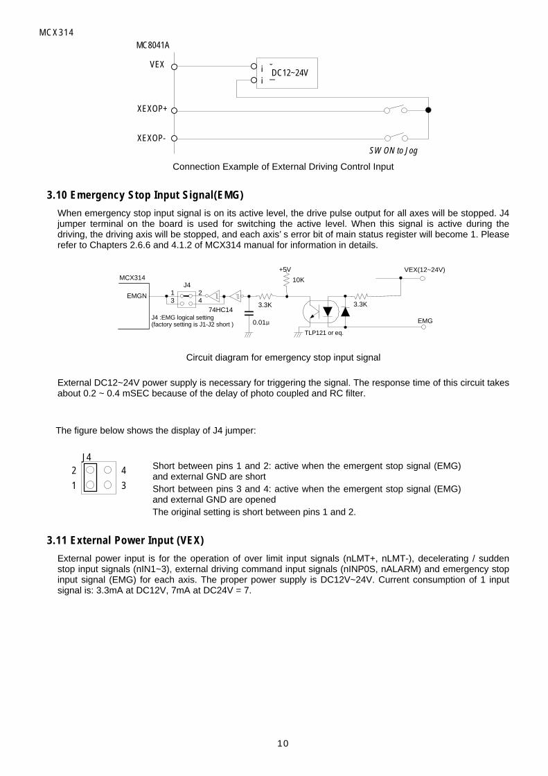
3.10 Emergency Stop Input Signal(EMG)
When emergency stop input signal is on its active level, the drive pulse output for all axes will be stopped. J4jumper terminal on the board is used for switching the active level. When this signal is active during thedriving, the driving axis will be stopped, and each axis’ s error bit of main status register will become 1. Pleaserefer to Chapters 2.6.6 and 4.1.2 of MCX314 manual for information in details.
MCX314
3.3K3.3K
VEX(12~24V)+5V
TLP121 or eq.
10K
EMGN
EMG0.01µ
74HC14
J4
J4 :EMG logical setting(factory setting is J1-J2 short )
13
24
Circuit diagram for emergency stop input signal
External DC12~24V power supply is necessary for triggering the signal. The response time of this circuit takesabout 0.2 ~ 0.4 mSEC because of the delay of photo coupled and RC filter.
The figure below shows the display of J4 jumper:
J42
1
4
3
Short between pins 1 and 2: active when the emergent stop signal (EMG)and external GND are shortShort between pins 3 and 4: active when the emergent stop signal (EMG)and external GND are openedThe original setting is short between pins 1 and 2.
3.11 External Power Input (VEX)
External power input is for the operation of over limit input signals (nLMT+, nLMT-), decelerating / suddenstop input signals (nIN1~3), external driving command input signals (nINP0S, nALARM) and emergency stopinput signal (EMG) for each axis. The proper power supply is DC12V~24V. Current consumption of 1 inputsignal is: 3.3mA at DC12V, 7mA at DC24V = 7.

MCX314
11
4. Interrupt Setting
Through J2 jumper terminal, total ten interrupt request signals at ISA bus can be connected.
When the interrupt occurs in MCX314, the interrupt request signal (IRQn) will become Hi level from Low level.After the status register 3 (nRR3) of the interrupted axis is read, this interrupt request signal will return to theLow level. Please refer to Chapters 2.5, 4.4 and 4.13 for interrupt functions.
MCX314INTN
+5V
74LS04
246810
13579
IRQ3IRQ4IRQ5IRQ6IRQ7
ISA BUS J2
1214161820
11113151719
IRQ10IRQ11IRQ12IRQ14IRQ15
The table below shows the shorted pins at J2 jumper corresponding to the interrupt request signals at ISA bus:
Interrupt Request Signal Short at J2 JumperIRQ3 between pins 1-2IRQ4 between pins 3-4IRQ5 between pins 5-6IRQ6 between pins 7-8IRQ7 between pins 9-10
IRQ10 between pins 11-12IRQ11 between pins 13-14IRQ12 between pins 15-16IRQ14 between pins 17-18IRQ15 between pins 19-20
The initial setting is shorted between pins 2 and 4, so there is no interrupt request to CPU.
[Note]For 74ALS04 is used for outputting interrupt signals, the interrupt request signals should not be used for otherdevices or for other I/O boards of PC.

MCX314
12
5. Connection Examples for Motor Drivers
5.1. Connection with Stepper Motor Drivers
The figure below is the example of MC8041A connected to a 5-phase micro-step driver, KR515M,manufactured by TECHNO DRIVE.
XP+P
XP+N
XP-P
XP-N
XOUT4
XOUT5
XINOP
XINON
GND
F+
F-
R+
R-
H.O.+
H.O.-
D.S.+
D.S.-
Z.P.-
Z.P.+
KR515MMC8041A
CW Pulse
CCW Pulse
Hold Off
M1/M2 select
Timing Output
Note 1: J3 of MC8041A is set at +5V output side for output terminals XP+P and XP-P. Please be verycareful that the external noise may happen during the wiring.
Note 2: Hold off, M1 / M2 select and timing output can be wired if necessary. The hold off and M1 /M2 selectsignals can be controlled by writing 0 and 1 into bits D8 and D9 of WR3 register of MCX314. Fortiming output signal, the signal level can be read through RR4 and RR5 registers.
The figure below is the example of MC8041A connected to UPK series stepper drivers manufactured byORIENTAL.
XP+P
XP+N
XP-P
XP-N
XOUT4
VEX
XIN1
XALARM
CW+
CW-
CCW+
CCW-
H.OFF+
H.OFF-
COM
O. HEAT
UPK seriesMC8041A
CW Pulse
CCW Pulse
Hold Off
Timing OutputTIMMING
GND
Over Heat
+DC24V
-
2KΩ/1w
Note 1: Hold off, timing output and over heat can be wired if necessary. The hold off signal can be controlled bywriting 0 and 1 into bit D8 of WR3 register of MCX314.For timing output signal, the home position searching can beperformed through the bits D0 and D1 of WR1 register mode setting. For over heat signal, the alarm function canbe performed through the bits D12 and D13 of WR2 register mode setting. For timing output and over heat signals,the signal level can be read through RR4 and RR5 registers.
Note 2: The user can use twist pair cable for long-distance connection or for a strong noise circumstance.

MCX314
13
5.2 Connection with Pulse-type Servo Motor Drives
The figure below is the example of MC8041A connected to MINAS XX series AC servo driver manufacturedby PANASONIC.
XP+P
XP+N
XP-P
XP-N
CW+
CW-
CCW+
CCW-
MINAS XX series CNI/FMC8041AI/O Connector
CW Pulse
CCW Pulse
XECAP
XECAN
XECBP
XECBN
XINOP
XINON
OA+
OA-
OB+
OB-
OZ+
OZ-
GND GND
XOUT4
XOUT5
XOUT6
GND
SRV-ON
CL
A-CLR
COM-
COM+
VEX
XIN3
XALARM
XINPOS
S-RDY
ALM
COIN
+DC24V
-
XLMT+
XLMT-
XIN1
CW DIR. LIMIT
CCW DIR. LIMIT
HOME
Encoder Phase A
Encoder Phase B
Encoder Phase Z
Servo On
Error Counter Clear
Alarm Clear
Servo Ready
Servo Alarm
Completing Position
Near by HOMEXIN2
Note 1: The servo driver should be engaged in position control mode and the pulse input is set the CW/CCWpulse mode. This connection is not proper for pulse / direction mode because the t6 time will not beenough.
Note 2: Encoder A / B phase can be connected when the real position counter of MCX314 is used for counting.It is not necessary to connect the real position data at CPU side, neither to connect other signals.
Note 3: The user can use twist pair cable for long-distance connection or for a strong noise circumstance.

MCX314
14
6. I/O Signal Timing
6.1 Power-on Reset
Low
Hi
Invalid
+5VRESDRV
nP±P
nP±N
nOUT4~7
Read/Write
OFF
Valid
¬ Drive pulse output signals (nP ± P, nP ± N) and general purpose output signals (nOUT4 ~ 7) will bedetermined after 250 nSEC from the reset signal of ISA bus (RESDRV) rising.
For data reading and writing is possible from 500 nSEC the reset signal (RESDRV) ¡ õ.
6.2 Individual Driving
1st pulse 2nd pulse
BUSYN
nPP±P
Pre state
nPP-Pdirection signal
←Interpolation drive command write in
Valid level
¬ The maximum time from the driving command write-in to the first pulse starting is about 650nSEC.® When the drive output pulse type is 1-pulse 1-direction, the direction signal (nP-P) will be in its valid levelwithin maximum 275 nSEC, and then first pulse will be output within 375 nSEC after the direction signal is inits valid level.
6.3 Interpolation Driving
1st pulse 2nd pulse
BUSYN
nPP±P
Valid level Valid levelNot stable Not stableNot stable
nPP-Pdirection signal
←Interpolation drive command write in
¬ After interpolation command is written, the first pulse will be output within 775 nSEC. When the drive output pulse type is 1-pulse 1-direction, the direction signal (nP-P) will be in its valid levelbefore and after 125 mSEC once the drive pulse is on the Hi level.

MCX314
15
6.4 Input Pulse Timing
n A/B Quadrature Pulse Input
nECAP
nECBP
Counting up Counting down
nECAN
nECBN
¬ Minimum time difference between EC-A and EC-B: 200 nSEC.
n Up / Down Pulse Input
nECAP
nECAN
nECBP
nECBN
¬ Minimum Up / Down pulse width: 130 nSEC Minimum UpÖDown pulse Interval: 260nSEC® Minimum Up / Down pulse cycle: 260 nSEC
MCX314
16
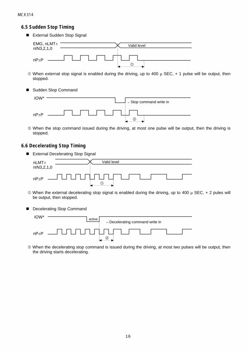
6.5 Sudden Stop Timing
n External Sudden Stop Signal
nP±P
Valid level
EMG, nLMT±nIN3,2,1,0
¬ When external stop signal is enabled during the driving, up to 400 µ SEC, + 1 pulse will be output, thenstopped.
n Sudden Stop Command
nP±P
IOW*←Stop command write in
When the stop command issued during the driving, at most one pulse will be output, then the driving isstopped.
6.6 Decelerating Stop Timing
n External Decelerating Stop Signal
nP±P
nLMT±nIN3,2,1,0
Valid level
¬ When the external decelerating stop signal is enabled during the driving, up to 400 µ SEC, + 2 pules willbe output, then stopped.
n Decelerating Stop Command
nP±P
activeIOW*←Decelerating command write in
When the decelerating stop command is issued during the driving, at most two pulses will be output, thenthe driving starts decelerating.

MCX314
17
7. Jumper and Switch Layout
J3
J2
SW2 SW1
J1 J4
1 4
3 6 +5V 24
2216
1 3 3119171 3
2 4 1820 42 42
ISA BUS
161163 11
22.1
92.2
120
2.54 X 1763.469.85
2.54 X 30
48 8110
18.63.2
31
SW1,2 : I/O address setting switches (see Chapter 2).J1 : J1-2 short circuit (initial setting) -- Please don’ t change.J2 : jumper for interrupt request signal settingJ3 : jumper for drive pulse / +5V switching (see Chapter 3.3)J4 : jumper for selecting EMG signal active level (see Chapter 3.9)

MCX314
18
8. Specifications
<Axial Control4 axes
< ISA Bus InterfaceData Bus 16 bytesI/O Address 16 bytesInterrupt IRQ3, 4, 5, 6, 7, 10, 11, 12, 14, 15 connectable
< InterpolationLinear Interpolation -- any 2 / 3 of 4 axesRange: -8,388,608 ~ +8,388,607; Accuracy: ¡ Ó0.5LSB; Speed: 1PPS ~ 4MPPS
Circular Interpolation -- any 2 of 4 axesRange: -8,388,608 ~ +8,388,607; Accuracy: ¡ Ó1LSB; Speed: 1PPS ~ 4MPPS
Bit Pattern Interpolation -- any 2 / 3 of 4 axes, for CPU calculation
Continuous Interpolation: performing linear and circular interpolations continuallyHighest drive speed of continuous interpolation: 2MHz
Other functions: interpolating axes selection, constant surface speed control, interpolating steps performance
for each axis…
<Drive-pulse OutputPulse Output Interface line driver (26LS31) outputPulse Output Speed Range 1PPS ~ 4MPPSPulse Output Accuracy within ± 0.1% (according to the setting speed)Jerk 954 ~ 31.25¡ Ñ109PPS/S2
Accelerating / Decelerating Speed 125 ~ 500¡ Ñ106PPS/S
Drive Speed 1 ~ 4¡ Ñ106 PPSOutput-pulse Number 0 ~ 268435455 / unlimitedSpeed Profile quadrature / trapezoidal / parabolic S-curveIndex Drive Deceleration Mode auto / manualOutput-pulse numbers and drive speeds changeable during the drivingIndependent 2-pulse system or 1-pulse 1-direction system selectableLogical levels of pulse selectable
<Encoder A / B / Z Phase InputPulse Input Interface: high-speed photo-coupler input; line driver connectableA/B quadrature pulse style or Up/Down pulse style selectablePulse of 1, 2 and 4 divisions selectable (A/B quadrature pulse style)
<Position CounterLogical Position Counter (for output pulse): 32-bitReal Position Counter (for input pulse): 32-bitData reading and writing possible
<Compare RegisterCOMP+ & COMP-Status and signal outputs for the comparisons of position countersSoftware limit functioned
MCX314
19
< Interrupt (Interpolations Excluded)The factors of occurring interrupt:..the drive-pulse outputting..the start / finish of a consistent-speed drive during the accelerating / decelerating driving..the end of the driving..the volume of position counter¡ Ùthe changed volume of COMP-
..the volume of position counter¡ Õthe changed volume of COMP-
..the volume of position counter¡ Ùthe changed volume of COMP+
..the volume of position counter¡ Õthe changed volume of COMP+Enable / disable for these factors selectable
<External Signal for DrivingEXPP and EXPM signals for fixed pulse / continuous driveInput Interface: photo-coupler + CR filter loop (mechanical connector connectable)
<External Decelerating / Sudden Stop Signal4 points (IN0 ~ 3) for each axis (IN0 for encoder Z phase)Input Interface: photo-coupler + CR filter loop (IN0: high-speed photo-coupler input)Enable / disable and logical levels selectable
<Servo Motor Input SignalALARM (alarm), INPOS (in-position)Input Interface: photo-coupler + CR filter loopEnable / disable and logical levels selectable
<General Output Signal4 points (OUT4 ~ 7) for each axis (or used for Drive Status Signals)Output Interface: 74LS06 open collector output
<Drive Status Signal OutputASND (speed accelerating), DSND (speed decelerating),CMPP (position¡ ÙCOMP+), CMPM (position¡ ÕCOMP-)Drive status and status registers readable
<Limit Signal Input2 points, for each + and - sideInput Interface: photo-coupler + CR filter loopLogical levels and decelerating / sudden stop selectable
<Emergency Stop Signal InputEMG, 1 point for 4 axesInput Interface: photo-coupler + CR filter loopJumper logical levels selectable
Operating Temperature 0°C ~ +45°C (30°F ~120°F)Voltage +5V ± 5% (max. power consumption: 700mA)External Power Supply DC12V ~ 24VBoard Size 161¡ Ñ121.9mm (connector excluded)I/O Connector Style FX2B-100PA-1.27DS (HIROSE)Attachment 1.2m cable, connector: FX2B-100SA-1.2R (HIROSE)

MCX314
20
MCX3144-Axis Motion Control IC

MCX314
21
Contents1. OUTLINE .. . . . . . . . . . . . . . . . . . . . . . . . . . . . . . . . . . . . . . . . . . . . . . . . . . . . . . . . . . . . . . . . . . . . . . . . . . . . . . . . . . . . . . . . . . . . . . . . . . . . . . . . . . . . . . . . 1
2. The Descriptions of Functions. . . . . . . . . . . . . . . . . . . . . . . . . . . . . . . . . . . . . . . . . . . . . . . . . . . . . . . . . . . . . . . . . . . . . . . . . . . . . . . . . . . . . . . . . . . . . 4
2.1 Pulse Output Command .. . . . . . . . . . . . . . . . . . . . . . . . . . . . . . . . . . . . . . . . . . . . . . . . . . . . . . . . . . . . . . . . . . . . . . . . . . . . . . . . . . . . . . . . . . . . . . 42.1.1 Fixed Pulse Driv ing Output . . . . . . . . . . . . . . . . . . . . . . . . . . . . . . . . . . . . . . . . . . . . . . . . . . . . . . . . . . . . . . . . . . . . . . . . . . . . . . 42.1.2 Continuous Pulse Driving Output. . . . . . . . . . . . . . . . . . . . . . . . . . . . . . . . . . . . . . . . . . . . . . . . . . . . . . . . . . . . . . . . . . . . . . . 5
2.2 Speed Curve. . . . . . . . . . . . . . . . . . . . . . . . . . . . . . . . . . . . . . . . . . . . . . . . . . . . . . . . . . . . . . . . . . . . . . . . . . . . . . . . . . . . . . . . . . . . . . . . . . . . . . . . . . . . 52.2.1 Constant Speed Driving . . . . . . . . . . . . . . . . . . . . . . . . . . . . . . . . . . . . . . . . . . . . . . . . . . . . . . . . . . . . . . . . . . . . . . . . . . . . . . . . . . . 52.2.2 Trapezoidal Driv ing . . . . . . . . . . . . . . . . . . . . . . . . . . . . . . . . . . . . . . . . . . . . . . . . . . . . . . . . . . . . . . . . . . . . . . . . . . . . . . . . . . . . . . . . . 62.2.3 S-curve Accelerat ion/Decelerat ion Driv ing . . . . . . . . . . . . . . . . . . . . . . . . . . . . . . . . . . . . . . . . . . . . . . . . . . . . . . . . . 72.2.4 Pulse Width and Speed Accuracy . . . . . . . . . . . . . . . . . . . . . . . . . . . . . . . . . . . . . . . . . . . . . . . . . . . . . . . . . . . . . . . . . . . . . . 9
2.3 Posit ion Control . . . . . . . . . . . . . . . . . . . . . . . . . . . . . . . . . . . . . . . . . . . . . . . . . . . . . . . . . . . . . . . . . . . . . . . . . . . . . . . . . . . . . . . . . . . . . . . . . 112.3.1 Logic Posit ion Counter and Real posit ion Counter . . . . . . . . . . . . . . . . . . . . . . . . . . . . . . . . . . . . . . . . . . . . . 112.3.2 Compare Register and Software Limit . . . . . . . . . . . . . . . . . . . . . . . . . . . . . . . . . . . . . . . . . . . . . . . . . . . . . . . . . . . . . . 11
2.4 Interpolat ion . . . . . . . . . . . . . . . . . . . . . . . . . . . . . . . . . . . . . . . . . . . . . . . . . . . . . . . . . . . . . . . . . . . . . . . . . . . . . . . . . . . . . . . . . . . . . . . . . . . . . . 122.4.1 Linear Interpolat ion . . . . . . . . . . . . . . . . . . . . . . . . . . . . . . . . . . . . . . . . . . . . . . . . . . . . . . . . . . . . . . . . . . . . . . . . . . . . . . . . . . . . . . . 122.4.2 Circular Interpolat ion . . . . . . . . . . . . . . . . . . . . . . . . . . . . . . . . . . . . . . . . . . . . . . . . . . . . . . . . . . . . . . . . . . . . . . . . . . . . . . . . . . . . . 142.4.3 The Bit Pattern Interpolat ion . . . . . . . . . . . . . . . . . . . . . . . . . . . . . . . . . . . . . . . . . . . . . . . . . . . . . . . . . . . . . . . . . . . . . . . . . . 162.4.4 Constant Vector Speed .. . . . . . . . . . . . . . . . . . . . . . . . . . . . . . . . . . . . . . . . . . . . . . . . . . . . . . . . . . . . . . . . . . . . . . . . . . . . . . . . . 192.4.5 Continuous Interpolat ion . . . . . . . . . . . . . . . . . . . . . . . . . . . . . . . . . . . . . . . . . . . . . . . . . . . . . . . . . . . . . . . . . . . . . . . . . . . . . . . . 212.4.6 The Accelerat ion / Decelerat ion Control in Interpolat ion. . . . . . . . . . . . . . . . . . . . . . . . . . . . . . . . . . . . . 242.4.6 Single-step interpolat ion ( from Command or External Signal) . . . . . . . . . . . . . . . . . . . . . . . . . . . . . 27
2.5 Interrupt . . . . . . . . . . . . . . . . . . . . . . . . . . . . . . . . . . . . . . . . . . . . . . . . . . . . . . . . . . . . . . . . . . . . . . . . . . . . . . . . . . . . . . . . . . . . . . . . . . . . . . . . . . . . 282.6 Other Funct ions. . . . . . . . . . . . . . . . . . . . . . . . . . . . . . . . . . . . . . . . . . . . . . . . . . . . . . . . . . . . . . . . . . . . . . . . . . . . . . . . . . . . . . . . . . . . . . . . . . 29
2.6.1 Driv ing By External Pulses . . . . . . . . . . . . . . . . . . . . . . . . . . . . . . . . . . . . . . . . . . . . . . . . . . . . . . . . . . . . . . . . . . . . . . . . . . . . . 292.6.2 Pulse Output Type Select ion . . . . . . . . . . . . . . . . . . . . . . . . . . . . . . . . . . . . . . . . . . . . . . . . . . . . . . . . . . . . . . . . . . . . . . . . . . 302.6.3 Pulse Input Type Select ion . . . . . . . . . . . . . . . . . . . . . . . . . . . . . . . . . . . . . . . . . . . . . . . . . . . . . . . . . . . . . . . . . . . . . . . . . . . . . 302.6.4 Hardware Limit Signals . . . . . . . . . . . . . . . . . . . . . . . . . . . . . . . . . . . . . . . . . . . . . . . . . . . . . . . . . . . . . . . . . . . . . . . . . . . . . . . . . . 302.6.5 Interface to Servo Motor Drivers . . . . . . . . . . . . . . . . . . . . . . . . . . . . . . . . . . . . . . . . . . . . . . . . . . . . . . . . . . . . . . . . . . . . . 312.6.6 Emergency Stop . . . . . . . . . . . . . . . . . . . . . . . . . . . . . . . . . . . . . . . . . . . . . . . . . . . . . . . . . . . . . . . . . . . . . . . . . . . . . . . . . . . . . . . . . . . 312.6.7 Status Output . . . . . . . . . . . . . . . . . . . . . . . . . . . . . . . . . . . . . . . . . . . . . . . . . . . . . . . . . . . . . . . . . . . . . . . . . . . . . . . . . . . . . . . . . . . . . . . 312.6.8 General Purpose Output. . . . . . . . . . . . . . . . . . . . . . . . . . . . . . . . . . . . . . . . . . . . . . . . . . . . . . . . . . . . . . . . . . . . . . . . . . . . . . . . . 31
3. Pin Assignments and Signal Descript ion . . . . . . . . . . . . . . . . . . . . . . . . . . . . . . . . . . . . . . . . . . . . . . . . . . . . . . . . . . . . . . . . . . . . . 33
4. Register . . . . . . . . . . . . . . . . . . . . . . . . . . . . . . . . . . . . . . . . . . . . . . . . . . . . . . . . . . . . . . . . . . . . . . . . . . . . . . . . . . . . . . . . . . . . . . . . . . . . . . . . . . . . . . . . . 38
4.1 Register Address by 16-bit Data Bus . . . . . . . . . . . . . . . . . . . . . . . . . . . . . . . . . . . . . . . . . . . . . . . . . . . . . . . . . . . . . . . . . . . . . 384.2 Register Address by 8-bit Data Bus . . . . . . . . . . . . . . . . . . . . . . . . . . . . . . . . . . . . . . . . . . . . . . . . . . . . . . . . . . . . . . . . . . . . . . . 404.3 Command Register: WR0 .. . . . . . . . . . . . . . . . . . . . . . . . . . . . . . . . . . . . . . . . . . . . . . . . . . . . . . . . . . . . . . . . . . . . . . . . . . . . . . . . . . . . 414.4 Mode Register1: WR1 .. . . . . . . . . . . . . . . . . . . . . . . . . . . . . . . . . . . . . . . . . . . . . . . . . . . . . . . . . . . . . . . . . . . . . . . . . . . . . . . . . . . . . . . . 414.5 Mode Register2: WR2 .. . . . . . . . . . . . . . . . . . . . . . . . . . . . . . . . . . . . . . . . . . . . . . . . . . . . . . . . . . . . . . . . . . . . . . . . . . . . . . . . . . . . . . . . 424.6 Mode Register3: WR3 .. . . . . . . . . . . . . . . . . . . . . . . . . . . . . . . . . . . . . . . . . . . . . . . . . . . . . . . . . . . . . . . . . . . . . . . . . . . . . . . . . . . . . . . . 434.7 Output Register: WR4 .. . . . . . . . . . . . . . . . . . . . . . . . . . . . . . . . . . . . . . . . . . . . . . . . . . . . . . . . . . . . . . . . . . . . . . . . . . . . . . . . . . . . . . . . 454.8 Interpolat ion Mode Register: WR5 .. . . . . . . . . . . . . . . . . . . . . . . . . . . . . . . . . . . . . . . . . . . . . . . . . . . . . . . . . . . . . . . . . . . . . . . 454.9 Data Register: WR6/WR7 .. . . . . . . . . . . . . . . . . . . . . . . . . . . . . . . . . . . . . . . . . . . . . . . . . . . . . . . . . . . . . . . . . . . . . . . . . . . . . . . . . . . 464.10 Main Status Register: RR0 .. . . . . . . . . . . . . . . . . . . . . . . . . . . . . . . . . . . . . . . . . . . . . . . . . . . . . . . . . . . . . . . . . . . . . . . . . . . . . . . . 474.11 Status Register 1: RR1 .. . . . . . . . . . . . . . . . . . . . . . . . . . . . . . . . . . . . . . . . . . . . . . . . . . . . . . . . . . . . . . . . . . . . . . . . . . . . . . . . . . . . . 484.12 Status Register 2: RR2 .. . . . . . . . . . . . . . . . . . . . . . . . . . . . . . . . . . . . . . . . . . . . . . . . . . . . . . . . . . . . . . . . . . . . . . . . . . . . . . . . . . . . . 494.13 Status Register 3: RR3 .. . . . . . . . . . . . . . . . . . . . . . . . . . . . . . . . . . . . . . . . . . . . . . . . . . . . . . . . . . . . . . . . . . . . . . . . . . . . . . . . . . . . . 494.14 Input Register: RR4 / RR5.. . . . . . . . . . . . . . . . . . . . . . . . . . . . . . . . . . . . . . . . . . . . . . . . . . . . . . . . . . . . . . . . . . . . . . . . . . . . . . . . . 504.15 Data-Read Register: RR6 / RR7 .. . . . . . . . . . . . . . . . . . . . . . . . . . . . . . . . . . . . . . . . . . . . . . . . . . . . . . . . . . . . . . . . . . . . . . . . . 50
5. Command Lists . . . . . . . . . . . . . . . . . . . . . . . . . . . . . . . . . . . . . . . . . . . . . . . . . . . . . . . . . . . . . . . . . . . . . . . . . . . . . . . . . . . . . . . . . . . . . . . . . . . . . . . 51
6. Commands for Data Wri t ing . . . . . . . . . . . . . . . . . . . . . . . . . . . . . . . . . . . . . . . . . . . . . . . . . . . . . . . . . . . . . . . . . . . . . . . . . . . . . . . . . . . . . . 53
6.1 Range Sett ing . . . . . . . . . . . . . . . . . . . . . . . . . . . . . . . . . . . . . . . . . . . . . . . . . . . . . . . . . . . . . . . . . . . . . . . . . . . . . . . . . . . . . . . . . . . . . . . . . . . . 536.2 S-curve Accelerat ion Rate Sett ing . . . . . . . . . . . . . . . . . . . . . . . . . . . . . . . . . . . . . . . . . . . . . . . . . . . . . . . . . . . . . . . . . . . . . . . . 536.3 Accelerat ion Sett ing. . . . . . . . . . . . . . . . . . . . . . . . . . . . . . . . . . . . . . . . . . . . . . . . . . . . . . . . . . . . . . . . . . . . . . . . . . . . . . . . . . . . . . . . . . . . 546.4 Decelerat ion Sett ing. . . . . . . . . . . . . . . . . . . . . . . . . . . . . . . . . . . . . . . . . . . . . . . . . . . . . . . . . . . . . . . . . . . . . . . . . . . . . . . . . . . . . . . . . . . . 546.5 Ini t ia l Speed Sett ing . . . . . . . . . . . . . . . . . . . . . . . . . . . . . . . . . . . . . . . . . . . . . . . . . . . . . . . . . . . . . . . . . . . . . . . . . . . . . . . . . . . . . . . . . . . 546.6 Drive Speed Sett ing . . . . . . . . . . . . . . . . . . . . . . . . . . . . . . . . . . . . . . . . . . . . . . . . . . . . . . . . . . . . . . . . . . . . . . . . . . . . . . . . . . . . . . . . . . . . 55

MCX314
22
6.7 Output Pulse Number / Interpolat ion Finish Point Sett ing . . . . . . . . . . . . . . . . . . . . . . . . . . . . . . . . . . . . . . . . . 556.8 Manual Decelerat ing Point Sett ing . . . . . . . . . . . . . . . . . . . . . . . . . . . . . . . . . . . . . . . . . . . . . . . . . . . . . . . . . . . . . . . . . . . . . . . . 556.9 Circular Center Sett ing . . . . . . . . . . . . . . . . . . . . . . . . . . . . . . . . . . . . . . . . . . . . . . . . . . . . . . . . . . . . . . . . . . . . . . . . . . . . . . . . . . . . . . . . 566.10 Logical Posit ion Counter Sett ing . . . . . . . . . . . . . . . . . . . . . . . . . . . . . . . . . . . . . . . . . . . . . . . . . . . . . . . . . . . . . . . . . . . . . . . . . 566.11 Real posit ion Counter Sett ing . . . . . . . . . . . . . . . . . . . . . . . . . . . . . . . . . . . . . . . . . . . . . . . . . . . . . . . . . . . . . . . . . . . . . . . . . . . . . 566.12 COMP+ Register Sett ing . . . . . . . . . . . . . . . . . . . . . . . . . . . . . . . . . . . . . . . . . . . . . . . . . . . . . . . . . . . . . . . . . . . . . . . . . . . . . . . . . . . . 566.13 COMP− Register Sett ing . . . . . . . . . . . . . . . . . . . . . . . . . . . . . . . . . . . . . . . . . . . . . . . . . . . . . . . . . . . . . . . . . . . . . . . . . . . . . . . . . . . . 566.14 Accelerat ion Counter Offsett ing . . . . . . . . . . . . . . . . . . . . . . . . . . . . . . . . . . . . . . . . . . . . . . . . . . . . . . . . . . . . . . . . . . . . . . . . . . 576.15 NOP (Used for Axis Switching) . . . . . . . . . . . . . . . . . . . . . . . . . . . . . . . . . . . . . . . . . . . . . . . . . . . . . . . . . . . . . . . . . . . . . . . . . . . 57
7. Commands for Reading Data . . . . . . . . . . . . . . . . . . . . . . . . . . . . . . . . . . . . . . . . . . . . . . . . . . . . . . . . . . . . . . . . . . . . . . . . . . . . . . . . . . . . 58
7.1 Logical Posit ion Counter Reading . . . . . . . . . . . . . . . . . . . . . . . . . . . . . . . . . . . . . . . . . . . . . . . . . . . . . . . . . . . . . . . . . . . . . . . . . 587.2 Real posit ion Counter Reading . . . . . . . . . . . . . . . . . . . . . . . . . . . . . . . . . . . . . . . . . . . . . . . . . . . . . . . . . . . . . . . . . . . . . . . . . . . . . 587.3 Current Drive Speed Reading . . . . . . . . . . . . . . . . . . . . . . . . . . . . . . . . . . . . . . . . . . . . . . . . . . . . . . . . . . . . . . . . . . . . . . . . . . . . . . . 587.4 Current Accelerat ion / Decelerat ion Reading . . . . . . . . . . . . . . . . . . . . . . . . . . . . . . . . . . . . . . . . . . . . . . . . . . . . . . . . . . 58
8. Driv ing Commands .. . . . . . . . . . . . . . . . . . . . . . . . . . . . . . . . . . . . . . . . . . . . . . . . . . . . . . . . . . . . . . . . . . . . . . . . . . . . . . . . . . . . . . . . . . . . . . . . . 59
8.1 +Direct ion Fixed Pulse Driv ing . . . . . . . . . . . . . . . . . . . . . . . . . . . . . . . . . . . . . . . . . . . . . . . . . . . . . . . . . . . . . . . . . . . . . . . . . . . . . 598.2 -Direct ion Fixed Pulse Driv ing . . . . . . . . . . . . . . . . . . . . . . . . . . . . . . . . . . . . . . . . . . . . . . . . . . . . . . . . . . . . . . . . . . . . . . . . . . . . . . 598.3 +Direct ion Continuous Driving . . . . . . . . . . . . . . . . . . . . . . . . . . . . . . . . . . . . . . . . . . . . . . . . . . . . . . . . . . . . . . . . . . . . . . . . . . . . . . 598.4 -Direct ion Continuous Driving . . . . . . . . . . . . . . . . . . . . . . . . . . . . . . . . . . . . . . . . . . . . . . . . . . . . . . . . . . . . . . . . . . . . . . . . . . . . . . 608.5 Drive Status Holding . . . . . . . . . . . . . . . . . . . . . . . . . . . . . . . . . . . . . . . . . . . . . . . . . . . . . . . . . . . . . . . . . . . . . . . . . . . . . . . . . . . . . . . . . . . 608.6 Drive Status Holding Release / Finishing Status Clear. . . . . . . . . . . . . . . . . . . . . . . . . . . . . . . . . . . . . . . . . . . . . 608.7 Decelerat ing Stop . . . . . . . . . . . . . . . . . . . . . . . . . . . . . . . . . . . . . . . . . . . . . . . . . . . . . . . . . . . . . . . . . . . . . . . . . . . . . . . . . . . . . . . . . . . . . . . 608.8 Sudden Stop . . . . . . . . . . . . . . . . . . . . . . . . . . . . . . . . . . . . . . . . . . . . . . . . . . . . . . . . . . . . . . . . . . . . . . . . . . . . . . . . . . . . . . . . . . . . . . . . . . . . . . 60
9. Interpolat ion Commands .. . . . . . . . . . . . . . . . . . . . . . . . . . . . . . . . . . . . . . . . . . . . . . . . . . . . . . . . . . . . . . . . . . . . . . . . . . . . . . . . . . . . . . . . . 61
9.1 2-Axis Linear Interpolat ion . . . . . . . . . . . . . . . . . . . . . . . . . . . . . . . . . . . . . . . . . . . . . . . . . . . . . . . . . . . . . . . . . . . . . . . . . . . . . . . . . . . 619.2 3-Axis Linear Interpolat ion . . . . . . . . . . . . . . . . . . . . . . . . . . . . . . . . . . . . . . . . . . . . . . . . . . . . . . . . . . . . . . . . . . . . . . . . . . . . . . . . . . . 619.3 CW Circular Interpolat ion . . . . . . . . . . . . . . . . . . . . . . . . . . . . . . . . . . . . . . . . . . . . . . . . . . . . . . . . . . . . . . . . . . . . . . . . . . . . . . . . . . . . 619.4 CCW Circular Interpolat ion . . . . . . . . . . . . . . . . . . . . . . . . . . . . . . . . . . . . . . . . . . . . . . . . . . . . . . . . . . . . . . . . . . . . . . . . . . . . . . . . . . 619.5 2-Axis Bit Pattern Interpolat ion . . . . . . . . . . . . . . . . . . . . . . . . . . . . . . . . . . . . . . . . . . . . . . . . . . . . . . . . . . . . . . . . . . . . . . . . . . . . 619.6 3-Axis Bi t Pattern Interpolat ion Drive . . . . . . . . . . . . . . . . . . . . . . . . . . . . . . . . . . . . . . . . . . . . . . . . . . . . . . . . . . . . . . . . . . . . 629.7 BP Register Data Writ ing Enabl ing . . . . . . . . . . . . . . . . . . . . . . . . . . . . . . . . . . . . . . . . . . . . . . . . . . . . . . . . . . . . . . . . . . . . . . . 629.8 BP Register Data Writ ing Disabl ing . . . . . . . . . . . . . . . . . . . . . . . . . . . . . . . . . . . . . . . . . . . . . . . . . . . . . . . . . . . . . . . . . . . . . . . 629.9 BP Data Stack . . . . . . . . . . . . . . . . . . . . . . . . . . . . . . . . . . . . . . . . . . . . . . . . . . . . . . . . . . . . . . . . . . . . . . . . . . . . . . . . . . . . . . . . . . . . . . . . . . . . 629.10 BP Data Clear . . . . . . . . . . . . . . . . . . . . . . . . . . . . . . . . . . . . . . . . . . . . . . . . . . . . . . . . . . . . . . . . . . . . . . . . . . . . . . . . . . . . . . . . . . . . . . . . . . 639.11 Single Step Interpolat ion . . . . . . . . . . . . . . . . . . . . . . . . . . . . . . . . . . . . . . . . . . . . . . . . . . . . . . . . . . . . . . . . . . . . . . . . . . . . . . . . . . . 639.12 Decelerat ion Enabl ing . . . . . . . . . . . . . . . . . . . . . . . . . . . . . . . . . . . . . . . . . . . . . . . . . . . . . . . . . . . . . . . . . . . . . . . . . . . . . . . . . . . . . . . 639.13 Decelerat ion Disabl ing. . . . . . . . . . . . . . . . . . . . . . . . . . . . . . . . . . . . . . . . . . . . . . . . . . . . . . . . . . . . . . . . . . . . . . . . . . . . . . . . . . . . . . . 639.14 Interpolat ion Interrupt Clear . . . . . . . . . . . . . . . . . . . . . . . . . . . . . . . . . . . . . . . . . . . . . . . . . . . . . . . . . . . . . . . . . . . . . . . . . . . . . . . 63
10. Connect ion Examples. . . . . . . . . . . . . . . . . . . . . . . . . . . . . . . . . . . . . . . . . . . . . . . . . . . . . . . . . . . . . . . . . . . . . . . . . . . . . . . . . . . . . . . . . . . . . 64
10.1 Connect ion Example for 68000 CPU .. . . . . . . . . . . . . . . . . . . . . . . . . . . . . . . . . . . . . . . . . . . . . . . . . . . . . . . . . . . . . . . . . . . 6410.2 Connect ion Example for Z80 CPU .. . . . . . . . . . . . . . . . . . . . . . . . . . . . . . . . . . . . . . . . . . . . . . . . . . . . . . . . . . . . . . . . . . . . . . 6410.3 Connect ion Example . . . . . . . . . . . . . . . . . . . . . . . . . . . . . . . . . . . . . . . . . . . . . . . . . . . . . . . . . . . . . . . . . . . . . . . . . . . . . . . . . . . . . . . . . 6510.4 Pulse Output Interface. . . . . . . . . . . . . . . . . . . . . . . . . . . . . . . . . . . . . . . . . . . . . . . . . . . . . . . . . . . . . . . . . . . . . . . . . . . . . . . . . . . . . . . 6510.5 Connect ion Example for Input Signals . . . . . . . . . . . . . . . . . . . . . . . . . . . . . . . . . . . . . . . . . . . . . . . . . . . . . . . . . . . . . . . . . 6610.6 Connect ion Example for Encoder . . . . . . . . . . . . . . . . . . . . . . . . . . . . . . . . . . . . . . . . . . . . . . . . . . . . . . . . . . . . . . . . . . . . . . . . 66
11. Example Program .. . . . . . . . . . . . . . . . . . . . . . . . . . . . . . . . . . . . . . . . . . . . . . . . . . . . . . . . . . . . . . . . . . . . . . . . . . . . . . . . . . . . . . . . . . . . . . . . . 67
12. Electr ical Character ist ics. . . . . . . . . . . . . . . . . . . . . . . . . . . . . . . . . . . . . . . . . . . . . . . . . . . . . . . . . . . . . . . . . . . . . . . . . . . . . . . . . . . . . . . . 70
12.1 DC Characterist ics . . . . . . . . . . . . . . . . . . . . . . . . . . . . . . . . . . . . . . . . . . . . . . . . . . . . . . . . . . . . . . . . . . . . . . . . . . . . . . . . . . . . . . . . . . . . 7012.2 AC Characterist ic . . . . . . . . . . . . . . . . . . . . . . . . . . . . . . . . . . . . . . . . . . . . . . . . . . . . . . . . . . . . . . . . . . . . . . . . . . . . . . . . . . . . . . . . . . . . . 70
12.2.1 Clock . . . . . . . . . . . . . . . . . . . . . . . . . . . . . . . . . . . . . . . . . . . . . . . . . . . . . . . . . . . . . . . . . . . . . . . . . . . . . . . . . . . . . . . . . . . . . . . . . . . . . . . . . 7012.2.2 Read / Wri te Cycle . . . . . . . . . . . . . . . . . . . . . . . . . . . . . . . . . . . . . . . . . . . . . . . . . . . . . . . . . . . . . . . . . . . . . . . . . . . . . . . . . . . . . . 7112.2.3 BUSYN Signal . . . . . . . . . . . . . . . . . . . . . . . . . . . . . . . . . . . . . . . . . . . . . . . . . . . . . . . . . . . . . . . . . . . . . . . . . . . . . . . . . . . . . . . . . . . . . 7112.2.4 SCLK/Output Signal Timing . . . . . . . . . . . . . . . . . . . . . . . . . . . . . . . . . . . . . . . . . . . . . . . . . . . . . . . . . . . . . . . . . . . . . . . . . . 7112.2.5 Input Pulses . . . . . . . . . . . . . . . . . . . . . . . . . . . . . . . . . . . . . . . . . . . . . . . . . . . . . . . . . . . . . . . . . . . . . . . . . . . . . . . . . . . . . . . . . . . . . . . 7212.2.6 General Purpose Input / Output Signals . . . . . . . . . . . . . . . . . . . . . . . . . . . . . . . . . . . . . . . . . . . . . . . . . . . . . . . . . 72
13. Timing of Input / Output Signals . . . . . . . . . . . . . . . . . . . . . . . . . . . . . . . . . . . . . . . . . . . . . . . . . . . . . . . . . . . . . . . . . . . . . . . . . . . . . . 73
13.1 Power-On Reset. . . . . . . . . . . . . . . . . . . . . . . . . . . . . . . . . . . . . . . . . . . . . . . . . . . . . . . . . . . . . . . . . . . . . . . . . . . . . . . . . . . . . . . . . . . . . . . . 7313.2 Fixed Pulse or Continuous Driving . . . . . . . . . . . . . . . . . . . . . . . . . . . . . . . . . . . . . . . . . . . . . . . . . . . . . . . . . . . . . . . . . . . . . . 73

MCX314
23
13.3 Interpolat ion. . . . . . . . . . . . . . . . . . . . . . . . . . . . . . . . . . . . . . . . . . . . . . . . . . . . . . . . . . . . . . . . . . . . . . . . . . . . . . . . . . . . . . . . . . . . . . . . . . . . . 7413.4 Start Dr iv ing after Hold Command.. . . . . . . . . . . . . . . . . . . . . . . . . . . . . . . . . . . . . . . . . . . . . . . . . . . . . . . . . . . . . . . . . . . . . . 7413.5 Sudden Stop . . . . . . . . . . . . . . . . . . . . . . . . . . . . . . . . . . . . . . . . . . . . . . . . . . . . . . . . . . . . . . . . . . . . . . . . . . . . . . . . . . . . . . . . . . . . . . . . . . . . 7413.6 Decelerat ing Stop . . . . . . . . . . . . . . . . . . . . . . . . . . . . . . . . . . . . . . . . . . . . . . . . . . . . . . . . . . . . . . . . . . . . . . . . . . . . . . . . . . . . . . . . . . . . . 74
14. Pinout . . . . . . . . . . . . . . . . . . . . . . . . . . . . . . . . . . . . . . . . . . . . . . . . . . . . . . . . . . . . . . . . . . . . . . . . . . . . . . . . . . . . . . . . . . . . . . . . . . . . . . . . . . . . . . . . . . 76
15. Specif icat ions . . . . . . . . . . . . . . . . . . . . . . . . . . . . . . . . . . . . . . . . . . . . . . . . . . . . . . . . . . . . . . . . . . . . . . . . . . . . . . . . . . . . . . . . . . . . . . . . . . . . . . . 77
Appendix A: Speed Curve Prof i le . . . . . . . . . . . . . . . . . . . . . . . . . . . . . . . . . . . . . . . . . . . . . . . . . . . . . . . . . . . . . . . . . . . . . . . . . . . . . . . . . . . . 1


MCX314
1
1. OUTLINEMCX314 is a 4-axis motion control IC which can control 4 axes of either stepper motor or pulse type servodriveers for position, speed, and interpolation controls. All of the MCX314’ s function are controlled by specificregisters. There are command registers, data registers, status registers and mode registers.This motion control IC has the following built-in functions:
n Individual Control for 4 AxesEach of the four axes has identical function capabilities, and is controlled by the same method of operationwith constant speed, trapezoidal or S-curve driving.
n Speed ControlThe speed range of the pulse output is from 1PPS to 4MPPS for constant speed, trapezoidal or S-curveacceleration/deceleration driving. The accuracy of the frequency of the pulse output is less than +/- 0.1%(at CLK=16MHz). The speed of driving pulse output can be freely changed during the driving.
n S-curve Acceleration and DecelerationEach axis can be preset with S-curve or trapezoidal acceleration/deceleration individually. Using S-curvecommand will drive the output pulse in a parabolic shaped acceleration and deceleration. Besides these,MCX314 has a special method to prevent from the happening of triangular curve when S-curve iscommanded.
n Linear InterpolationAny 2 or 3 axes can be selected to perform linear interpolation. The position boundary is betweencoordinates -8,388,608 and +8,388,607, and the positioning error is within +/- 0.5 LSB (Least SignificantBit). The interpolation speed range is from 1 PPS to 4 MPPS.
n Circular InterpolationAny 2 axes can be selected to perform circular interpolation. The position boundary is between coordinates-8,388,608 and +8,388,607, and the positioning error is within +/- 1.0 LSB. The interpolation speed rangeis from 1 PPS to 4 MPPS.
n Bit Pattern InterpolationAny 2 or 3 axes can be selected to perform the bit pattern interpolation, and the interpolation data iscalculated by CPU; CPU writes the bit data into MCX314. Then, MCX314 outputs pulses continuously atthe preset driving speed. So, the user can process any interpolation curve by this mode.
n Continuous InterpolationDifferent interpolation methods can be used continuously, linear interpolation -> circularinterpolation -> linear interpolation …, The maximum driving speed of performing continuousinterpolation is 2 MHz.
n Constant Vector Speed ControlThis function performs a constant vector speed. During the interpolation driving, MCX314 can set a 1.414times pulse cycle for 2-axis simultaneous pulse output, and a 1.732-time pulse cycle for 3-axissimultaneous pulse output.
n Position ControlEach axis has a 32-bit logic position counter and a 32-bits real position counter. The logic positioncounter counts the output pulse numbers, and the real position counter counts the feedback pulse numbersfrom the external encoder or linear scale.
n Compare Register and Software LimitEach axis has two 32-bit compare registers for logical position counter and real position counter. Thecomparison result can be read from the status registers. The comparison result can be notified by aninterrupt signal. These registers can be also functioned as software limits.
n Driving by External SignalIt is possible to control each axis by external signals. The +/- direction fixed pulse driving and continuousdriving can be also performed through the external signals. This function is used for JOG or teachingmodes, and will share the CPU load.
n Input/ Output SignalEach axis has 4 points of input signals to perform deceleration and stop in driving. These input signals arefor high-speed near-by home search, home search and z-phase search during the home returning. Eachaxis is with 8 output points for general output.

MCX314
2
n Servo Motor Feedback SignalsEach axis includes input pins for servo feedback signals such as in-positioning, close loop positioningcontrol and servo alarm.
n Interrupt SignalsInterrupt signals can be generated when: (1). the start / finish of a constant speed drive during thetrapezoidal driving, (2). the end of driving, and (3). the compare result once higher / lower the border-linesof the position counter range. An interrupt signal can be also generated during the interpolation driving.
n Real Time MonitoringDuring the driving, the present status such as logical position, real position, drive speed, acceleration /deceleration, status of accelerating / decelerating and constant driving can be read.
n 8 or 16 Bits Data Bus SelectableMCX314 can be connected to either 8-bit or 16-bit CPU
Figure 1.1 is the IC functional block diagram. It consists of same functioned X, Y, Z and U axes controlsections and interpolation counting sections. Figure 1.2 is the functional block diagram of each axis controlsection.
Leaner Interpolation Counting Section
2 axes/3 axes
Circle InterpolationCounting Section
2 axes
Bit InterpolationCounting Section 2 axes/3 axes
Pulseseparate
AX1P+AX1P-AX2P+AX2P-AX3P+AX3P-
AX1P+AX1P-AX2P+AX2P-AX3P+AX3P-
AX1P+AX1P-
AX2P+AX2P-
Main axis pulseX Axis Control Section
INT
XP+XP-
Main axis pulseY Axis Control Section
INT
YP+YP-
Main axis pulseZ Axis Control Section
INT
ZP+ZP-
Main axis pulseU Axis Control Section
INT
UP+UP-
Interpolation ControlSection.
INT
Interrupt Generator
Command/DataInterpretation/
ProcessSection
XP+XP-
YP+YP-
ZP+ZP-
UP+UP-
CSNRDN
WRNA3~A0
D15~D0BUSYN
X AXISI/O
Y AXISI/O
U AXISI/O
Z AXISI/O
INTN
Figure 1.1 MCX314 Functional Block Diagram

MCX314
3
CommandOperatingSection
InterruptGenerator
Jerk Generator
ActionManagingSection
Input SignalManagement
Section
Compare RegisterCOMP+
Compare RegisterCOMP-
UP
Logical PositionCounter(32bit)
DOWN
UP
Real Position CounterDOWN
INT
LMTPLMTMINPOSALARMEMGN
IN3~0
P+
P-
EC-AEC-B
ExternalOperationSection.
EXPPEXPM
Acceleration/DecelerationGenerator
Speed Generator
P+Pulse Generator
P-
WaveChange
WaveChange
General outputOUT3~0
General outputOUT7~4
Main Axis Pulse
PP/PLS
PM/DIR
Sel
ecto
r
Sel
ecto
r
OUT3~0
OUT7~4
ExternalSignal
ExternalSignal
Note 1: EMGN is for all axes use.
Command/Data
ToInterpolateSection
Fig.1.2 Control Block Diagram

MCX314
4
2. The Descriptions of Functions
2.1 Pulse Output Command There are two kinds of pulse output commands: fixed pulse driving output and continuous pulse driving output.
2.1.1 Fixed Pulse Driving Output When host CPU writes a pulse numbers into MCX314 for fixed pulse driving, and configures theperformance such as acceleration / deceleration, speed. MCX314 will generate the pulses and output themautomatically. When output pulse numbers are equal to the command pulse numbers, MCX314 stops theoutput. The profile is showing in Fig.2-1. Concerning the execution of fixed pulse driving in acceleration / deceleration, it is necessary to set thefollowing parameters:
z Range R
z Acceleration/Deceleration A/D
z Initial Speed SV
z Driving Speed V
zOutput Pulse Numbers P
nChanging Output Pulse Numbers in Driving The output pulse numbers can be changed in the fixedpulse driving. If the command is for increasing the outputpulse, the pulse output profile is shown as Fig. 2.2 or 2.3.If the command is for decreasing the output pulses, theoutput pulse will be stopped immediately as shown in Fig.2.4. Furthermore, when in the S-curve acceleration/deceleration driving mode, the output pulse numberchange will occur to an incomplete deceleration S-curve.
nManual Setting Deceleration for fixed pulse Acceleration/Deceleration Driving As shown in Fig. 2.1, generally the deceleration of fixed pulse acceleration /deceleration driving iscontrolled automatically by MCX314. However, in the following situations, it should be preset thedeceleration point by the users.l The change of speed is too often in the trapezoidal fixed pulse acceleration/deceleration driving.l When use circular interpolation, bit pattern interpolation and continuous interpolation for acceleration
and deceleration. In case of manual deceleration, please set D0 bit of register WR3 to 1, and use command (07h) forpresetting deceleration point. As to the other operation, the setting is as same as that of fixed pulse driving.
Driving Speed
Initial Speed
Time
Auto Deceleration
Specific Output Pulse Finished
Fig. 2.1 Fixed Pulse Driving
Driving Speed
Initial Speed
Time
Change of Output Pulse
Fig. 2.2 Changing The Output Pulse Numbers in Drivingdeceleration
Fig. 2.3 Changing Command During Deceleration
Initial Speed
Time
Change of Output Pulse
Driving Speed
Initial Speed
Time
Change of Output Pulse
Fig.2.4 Changing The Lesser Pulse Numbers Than Output Pulse Stop

MCX314
5
nOffset Setting for Acceleration/Deceleration Driving The offset function can be used for compensating thepulses when the decelerating speed doesn’ t reach thesetting initial speed during the S-curve fixed pulse driving.MCX314 will calculate the acceleration / decelerationpoint automatically, and will arrange the pulse numbers inacceleration equal to that in deceleration. The method iscalculating the output acceleration pulses and comparingthem with the remaining pulses. When the remainingpulses are equal to or less the pulses in acceleration, itstart the deceleration.
When setting the offset for deceleration, MCX314 willstart deceleration early for the offset. The remainingpulses of offset will be driving output at the initial speed (see Fig. 2.5). The default value for offset is 8 when MCX314 power-on reset. It is not necessary to change the shift pulsevalue in the case of acceleration/deceleration fixed pulse driving.
2.1.2 Continuous Pulse Driving Output When the continuous driving is performed, MCX314 willdrive pulse output in a specific speed until stop commandor external stop signal is happened. The main application of continuous driving is: homesearching, teaching or speed control. Two stop commands are for stopping the continuousdriving. One is “decelerating stop” , and the other is“sudden stop” . Four input pins, IN3~IN0, of each axis can be connectedfor external decelerating and sudden stop signals. Enable/ disable, active levels and mode setting are possible.
nStop Condition for External Input IN3~IN0 in Continuous Driving The input pins IN3~IN0 can be used for home searching, near-by home searching and Z-phase searching .Enable / disable and logical levels can be set at WR1 of each axis. For the application of high-speed searching, the user can set MCX314 in the acceleration/decelerationcontinuous driving mode and enable IN1 in WR1. And then, MCX314 will perform the decelerating stopwhen the external signal IN1 is active. For the application of low-speed searching, the user can set MCX314 in the constant-speed continuousdriving and enable IN1. Then, MCX314 will perform the sudden stop when IN1 is active.
2.2 Speed Curve
The speed driving profile in MCX314 can be configured as constant speed driving, trapezoidal driving or S-curve acceleration/deceleration.
2.2.1 Constant Speed Driving When the driving speed set in MCX314 is lower than theinitial speed, the acceleration / deceleration will not beperformed, instead, a constant speed driving starts. If the user wants to perform the sudden stop when thehome sensor or encoder Z-phase signal is active, it isbetter not to perform the acceleration / decelerationdriving, but the low-speed constant driving from thebeginning. For processing constant speed driving, the followingparameters will be preset accordingly.
z Range R z Initial Speed SV z Drive Speed V ; Output Pulse Numbers P (Only applicable for the fixed pulse driving)
The items should be preset in accordance with the requirement.
Driving Speed
Initial Speed
Time
Shift Pulse
Fig.2.5 Remaining Pulse in Acc. / Dec. Fixed PulseDriving
Driving Speed
Initial Speed
Time
Stop Command orExternal Stop Signal
Fig.2.6 Continuos Driving
Driving Speed
Initial Speed
Time
Fig.2.7 Constant Speed Driving
Speed

MCX314
6
nExample for Parameter Setting of Constant Speed The constant speed is set 980 pps as shown in the right Figure.
z Range R = 8,000,000: Multiple(M) = 1 z Initial Speed SV=980: Initial Speed ≥ Driving Speed z Driving Speed V=980: Should be less than initial speed
Please refer each parameter in Chapter 6.
2.2.2 Trapezoidal Driving Trapezoidal driving is starting from the initial speed tothe designated drive speed. The accelerating pulseswill be counted, and the deceleration (automaticdeceleration) starts from the drive speed to initialspeed once the remaining pulse numbers are lessthan the accelerating pulse numbers. When the decelerating stop command is performedduring the acceleration, or when the pulse numbers ofthe fixed pulse drive do not reach the designated drivespeed, the driving will be decelerating duringacceleration, as show in Fig. 2.8. (triangle drivingprofile prevention, see appendix A3) Usually, the user should set the same acceleration and deceleration rates. For some cases, the accelerationand deceleration can be set individually by setting the D1 of WR3 to 1. When the deceleration is setindividually in fixed pulse driving, the automatic deceleration will not be performed, but the manualdeceleration is required. The user should set the bit D1 of Register WR3 as 1, then use deceleratingcommand (03h) to set the deceleration. When performing the trapezoidal driving, the following parameters should be preset.
z Range R z Acceleration A : Acceleration and deceleration ; Deceleration D : Option for individual deceleration. z Initial Speed SV z Driving Speed V ; Output Pulse Number P : Only for fixed pulse driving
The ; items should be preset in accordance with the requirement.
nThe example of setting Trapezoidal Driving Shown in the figure right hand side, acceleration is form theinitial speed 500 PPS to 15,000 PPS in 0.3 sec.
z Range R = 4,000,000; Multiple(M)= 2 z Acceleration A=193 (15,000-500/0.3 =48,333 48,333/125/M = 193) z Initial Speed SV = 250 (500/M = 250) z Drive Speed V = 7,500 (15,000/M = 7,500)
Please refer Chapter 6.
980
Time(SEC)
Speed(PPS)
Drive Speed
Initial Speed
Time
Acceleration(slope)
Fig.2.8 Trapezoidal Driving
Acceleration
output pulse is too low, notsuitable for the requirementof drive speed
15,000
500
Time(SEC)
Speed(PPS)
0.3

MCX314
7
2.2.3 S-curve Acceleration/Deceleration Driving In case of S-curve acceleration / deceleration driving,the acceleration profile is not linear. The value ofacceleration / deceleration is shaped as the trapezoid;see Fig. 2.9. In acceleration, there are three regions with differentacceleration values. At the beginning, the accelerationincrease linearly from 0 to the specific value A with aspecific rate of acceleration K, which shows thedriving speed increase parabolically in this region.Then, the driving speed increases in a constantacceleration in region b. And, in section c, theacceleration decelerates linearly to 0 with the rate ofdeceleration K. So the acceleration of S-curveincludes regions a, b and c. In deceleration, as same as acceleration, the drivingspeed decelerate parabolically in three regions d, eand f.
nComplete S-curve and Partial S-curve The desired driving speed is V. When V (speed in region a) ≤ speed in region a, the region b will disappear.This condition is called complete S-curve. Otherwise, it is called partial S-curve. Please check theparameters and examples in Appendix A. In order to execute S-curve acceleration / deceleration, the user has to set bit D2 of register WR3 to 1, andthe following parameters are necessary to be set.
z Range R z Jerk K z Acceleration A : The designated value of acceleration and deceleration ; Deceleration D : The designated deceleration value of individual setting z Initial Speed SV z Drive Speed V ; Output Pulse Number P : Used for fixed pulse driving
nThe Prevention of Triangle Driving Profile When the fixed pulse trapezoidal driving is performed, and also when the deceleration is performed beforethe acceleration stops, the triangle driving profile is coming out. The prevention of triangle driving profile inS-curve acceleration / deceleration driving will be discussed as follows. If the initial speed is 0, and if the rate of acceleration is a, then the speed at time t in acceleration regioncan be described as following.
v(t) = at2
Therefore, the total output pulse number p(t) from time0 to t is the integrated of speed.
p(t) = 1/3 x at3
The total output pulse is
(1/3+2/3+1+2/3+1+1/3) x at3 = 4 at3
so
p(t) = 1/12 (total pulse output) Therefore, when the output pulse in acceleration of S-curve is more than 1/12 of total output pulse,MCX314 will stop increasing acceleration and start to decrease the acceleration value.
Speed
Initial Speed
a
Time
TimeAcceleratio Deceleration
Acceleration/ Deceleration
b c d e f
Desired DriveSpeed (V)
Specific value(A)
Fig.2.9 S-Curve Acceleration/Deceleration Driving
Speed
Initial Speed
1 1
2/3 2/3
1/31/3
p(t)
Time
TimeAcc. Dec.
Acceleration
Fig. 2.10 The rule of 1/12 of Parabolic Acceleration/Deceleration
at2

MCX314
8
nThe Decelerating Stop for Preventing the Triangle Driving Profile in S-curve Driving When the decelerating stop is commanded, or whenthe external signals IN3~IN0 are active during the S-curve acceleration / deceleration driving, theacceleration rate is decreasing, then the decelerationstarts when the acceleration rate reaches 0.
nConstraints for S-curve Acceleration / Deceleration Drivingl The drive speed cannot be changed during the fixed pulse S-curve acceleration / deceleration driving.l When the fixed-pulse S-curve acceleration / deceleration driving is performed, the change of the output
pulse numbers during the deceleration will not result a normal S-curve driving profile.l In case of executing circular interpolation, bit pattern interpolation and continuous interpolation, S-
curve acceleration/deceleration cannot be executed normally.l If the S-curve output pulses run out before the deceleration to the initial speed, the user can use offset
function.l When the S-curve output pulses are decelerating to the initial speed, but still some pulses remains, the
user can modify the parameter K and driving speed V to avoid this situation.
nExample of Setting Parameters (Complete S-curve Acceleration /Deceleration) *Setting a complete S-curve acceleration to output the drive speed from 0 to 40K PPS in 0.4 sec. As shown in Fig. Ex.3, if complete S-curve acceleration is required, the driving must be 20K PPS at time0.2sec. And then, it will accelerate to 40K PPS at time 0.4sec. To calculate the maximum acceleration value acc. at time0.2sec, we know the speed at time 0.2sec is 20K PPS. So weget
20000PPS = 0.2sec x acc. /2 so, acc. = 200K PPS/sec To calculate the jerk, we get
200KPPS/0.2sec=1000KPPS/sec2
In a complete S-curve acceleration/deceleration, the speedcurve is depended on the jerk. Since the acceleration /deceleration does not exit in the partial S-curve, it should be preset over than 200KPPS/SEC.
z Range R = 800,000 ; multiple(M) = 10 z Jerk K = 625 ; ((62.5 x 10⁶)/625) x 10 = 1,000KPPS/SEC2
z Acceleration A = 160 ; 125 x 160 x 10 = 200KPPS z Initial Speed SV = 100 ; 100 x 10 = 1000KPPS z Drive Speed V = 4000 ; 4000x 10 = 40,000PPS
Please refer each parameter in Chapter 6.
Speed
Time
Time
Acceleration
Request for Decelerating Stop
Decrease the Acceleration value
Acc. become zero, Dec. begins
Fig. 2.11 Decelerating Stop During S-curve Acc./ Dec. Driving
Speed PPS
40000
20000
acc.=200K
0
0.2 0.4 SEC
0.2 0.4 SEC
0
20000PPS
AccelerationPPS/SEC

MCX314
9
nExample of Parameter Setting (Partial S-curve Acceleration / Deceleration) *Setting a partial S-curve acceleration to output the drivespeed from 0 to 40K PPS in 0.6 sec. At first, a parabolic accelerating is executed to 10KPPS in0.2 sec., then the linear acceleration goes up to 30KPPS,and then the parabolic acceleration reaches to 40KPPS. We get
10K PPS = Acceleration x 0.2sec / 2 Acceleration = 100K PPS/sec
And, the jerk is 100KPPS/sec/0.2sec=500KPPS/sec2
z Range R = 800,000 : multiple = 10
z Jerk K = 1250 : ((62.5 x 10⁶)/1250) x 10 =500 x 103 PPS/SEC 2
z Acceleration A = 80 : 125x80x10 =100x103
PPS/SEC z Initial Speed SV = 100 : 100 x 10 = 1000 PPS z Drive Speed V = 4,000 : 4,000 x 10 = 40,000 PPS
Please refer each parameter in Chapter 6.
2.2.4 Pulse Width and Speed AccuracynDuty Ratio of Driving Pulse The period time of + /- direction pulse driving of each axis is decided by system clock CLK. The tolerance iswithin ±1SCLK (For CLK=16MHz, the tolerance is ±125nSEC). Basically, the duty ratio of each pulse is 50% as show in Fig. 2.12. When the parameter setting isR=8,000,000 and V=1000 (Multiple=1, V=1000PPS), the driving pulse is 500uSEC on its Hi level and50uSEC on its Low level and the period is 1mSEC.
500µS 500µS
1.00mS
R = 8000000SV = 1000V = 1000
Fig. 2.12 Output of Drive Pulse (1000PPS)
However, during the acceleration / deceleration driving, the Low level pulse length is shorter than that of Hilevel pulse during the acceleration; the Low level pulse is longer than that of Hi level pulse during thedeceleration. See Fig. 2.13.
tHA tLA tHC tLC tHD tLDtHA>tLA tHC=tLC tHD<tLD
Acceleration Area Constant speed Area Deceleration Area
Fig. 2.13 Comparison of Drive Pulse Length in Acceleration / Deceleration
Speed PPS
40000
30000
100K
0
0.2 0.6 SEC
SEC
0
10000PPS
AccelerationPPS/SEC
0.4
10000
0.2 0.60.4

MCX314
10
nThe Accuracy of Drive Speed The clock(SCLK) running in MCX14 is half of external input clock(CLK). If CLK input is standard 16MHz,SCLK will be 8MHz. Therefore, the user had better driving the pulse speed in a exact multiple of SCLK period(125nSEC).Otherwise, the driving pulse will not very stable. The following table shows the frequency (speed) of drivingpulse of MCX314 can be, there are all exact the multiple of 125nSEC.
Multiple Drive Speed (PPS) Multiple Drive Speed (PPS) Multiple Drive Speed (PPS) Multiple Drive Speed (PPS)
11 727 K 95 84,211 995 8040 2 4.000 M 12 667 K 96 83,333 996 8032 3 2.667 M 13 615 K 97 82,474 997 8024 4 2.000 M 14 571 K 98 81,632 998 8016 5 1.600 M 15 533 K 99 80,808 999 8008 6 1.333 M 16 500 K 100 80,000 1000 8000 7 1.143 M 17 471 K 101 79,208 1001 7992 8 1.000 M 18 444 K 102 78,431 1002 7984 9 889 K 19 421 K 103 77,670 1003 7976
10 880K 20 400 K 104 76,923 1004 7968
As shown in the table above, it is not very stable to set any desired driving speed. However, MCX314 canmake any drive speed in using the following method. When the preset range value: R= 80,000 (Multiple=100), drive speed setting value: V=4900, the outputpulse is set 4900 x 100=490KPPS. From the able above, the output 490KPPS cannot be exactly madebecause the period of 490KPPS is 16.326 times of SCLK (125nSEC). Therefore, as shown in Figure 2.14, MCX314 combines 16 times and 17 times of SCLK period in a rate of674:326 to generate an average 490KPPS.
16 16 1716 16 1716
Fig. 2.14 The driving pulse of 490KPPS when SCLK is 8MHz
According to this method, MCX314 can generate a constant speed driving pulse in a very high accuracy. Ingeneral, the higher of the driving speed, the lower of the accuracy. But for MCX314, it still can maintainrelative accuracy when the driving speed is high. Actually, the accuracy of driving pulse is still within ±0.1%. Using oscilloscope for observing the driving pulse, we can find the tolerance about 1SCLK(125nSEC). Thisis no matter when putting the driving to a motor because the tolerance will be absorbed by the inertia ofmotor system.

MCX314
11
2.3 Position Control
Fig 2.15 is 1-axis position control block diagram. For each axis, there are two 32 bit up-and-down countersfor counting present positions and two comparison registers for comparing the present positions.
UPLogical Position Counter
(32bit) DOWN
COMP+ Register32Bit
WaveformTransformation
Selector
W/R
W/RUP
Real Position Counter (32bit) DOWN
COMP- Register32Bit
W
W
Com
pareWR2 Register/D5
Com
pare
PP +direction pulse
PM -direction pulse
ECA/PPIN
ECB/PMIN
RR1 register/D0CMPP
encoderfeedback pulse
RR1 register/D1CMPM
Fig. 2.15 Position Control Block Diagram
2.3.1 Logic Posit ion Counter and Real posit ion Counter The logic position counter is counting the driving pulses in MCX314. When one + direction plus is outputting,the counter will count-up 1; when one - direction pulse is outputting, the counter will count-down 1. The real position counter will count input pulse numbers from external encoder. The type of input pulse canbe either A/B quadrature pulse type or Up / Down pulse(CW/CCW) type (See Chapter 2.6.3). Host CPU can read or write these two counters any time. The counters are signed 32 bits, and the countingrange is between -2,147,483,648 ~ + 2,147,483,647. The negative is in 2’ s complement format. Thecounter value is random while resetting.
2.3.2 Compare Register and Software Limit Each axis has, as shown in Fig, 2.15, two 32-bit registers which can compare the logical positions with thereal positions. The logical position and real position counters are selected by bit D5 (CMPSL) of registerWR2. The main function of COMP+ Register is to check out the upper limit of logical / real position counter.When the value in the logical / real position counters are larger than that of COMP+ Register, bit D0 (CMP+)of register RR1 will become 1. On the other hand, COMP- Register is used for the lower limit of logical /real position counter. When the value of logical / real position counter become smaller than hat of COMP+Register, bit D1 (CMP-) of register RR1 will become 1. Fig. 2.16 is an example for COMP+ = 10000,COMP- = -10000.
0-1000 10000
CM CPRR1/D0=0RR1/D1=0
RR1/D0=0RR1/D1=1
RR1/D0=1RR1/D1=0
COMP+ register CP=10000COMP- register CM=-1000
Fig. 2.16 Example of COMP+/- Register Setting
COMP+ and COMP- registers can be used as software +/- limit. When D0 and D1bits of register WR2 areset to 1, it enables the software limit. In driving, if the value of logical / real counter is larger than COMP+,the decelerating stop will be performed, and D0 (SLMT+) of register RR2 will change to 1. If the value oflogical / actual counter is smaller than that of COMP+, the D0 bit of register RR2 will change to 0automatically. Host CPU can write the COMP+ and COMP- registers any time. However, when MCX314 isreset, the register values are random.

MCX314
12
2.4 Interpolation
This 4-axis motion control IC can perform any 2 / 3 axes linear interpolation, any 2 axes circularinterpolation and any 2 / 3 axes bit pattern interpolation. Bits D0, D1 (ax 1), D2, D3 (ax 2) and D4, D5 (ax 3)of register WR5 can be pointed for performing the interpolation. In the process of interpolation driving, allthe calculations will follow the main axis (ax1). So, the user has to set the parameters such as initial speedand drive speed of the main axis before performing the interpolation. During the linear interpolation, it is notnecessary to set the main axis as “ long axis” . After setting all of the parameters for interpolations, and writing the interpolation driving commands tocommand register WR0, the user can start the interpolation driving. During the interpolation driving, D8 (I-DRV) of main status register RR0 will become 1 during the interpolation, and it will become 0 when theinterpolation is finished. Also, during the interpolation driving, the bit n-DRV of the interpolating axis willbecome 1. The maximum drive speed is 4MPPS for linear, circular or bit pattern interpolation. For continuousinterpolation, the maximum drive speed is 2MPPS. ¡ Over Limit Error of Interpolation
When the hardware limit or the software limit of each axis is active during the interpolation driving, theinterpolation will stop. It the stop is occurred by errors, RR0 (main status register) will confirm the error bit ofthe designated interpolating axis. PR0 will become 1, and RR2 (error register) of this axis will be read out.Note: In case of circular or bit patter interpolation, the “active” of hardware or software limit, in either + or -direction, will stop the interpolation driving.¡ In-position Signal for Servo Motor During the interpolation driving, when the in-position signal (nINP0S) of each driving axis is active, and alsowhen the interpolation is finished, the INP0S signal of the axis is stand-by at its active level, and D8 (I-DRV)of RR0 register returns to 0.
2.4.1 Linear Interpolat ion Any 2 or 3 axes of the 4 axes can be set for linearinterpolation. To execute the linear interpolation, theuser can, according to the present point coordinates,set the finish point coordinates and the interpolationcommand(s) for 2 or 3 axes. As shows in Fig. 2.17 the proceeding for linearinterpolation is performing from the start point to thefinish point. For individual axis control, the command pulse numberis unsigned, and it is controlled by + direction commandor - direction command. For interpolation control, thecommand pulse number is signed. The resolution of linear interpolation is within ±0.5 LSB,as showen in Fig. 2.17. As shown in Fig. 2.18, it is an example for pulseoutput of the linear interpolation driving. Wedefine the longest distance movement ininterpolation is the “ long axis” . And the other is“short axis” . The long axis outputs an averagepulse train. The driving pulse of the short axisdepends on the long axis and the relationship ofthe two axes. The range for each axis is a 24-bit signedcounter, from -8,388,607 ~ +8,386,807. Note: The user cannot set -8,388,608.
±0.5LSB
5 10 15 200
5
10
Y Short axis
XLong axis
(20,9)
Fig. 2.17 The Position Accuracy for Linear Interpolation
XPPXPM
YPP
YPM
Long axis
Short axis
Fig. 2.18 The Example for Pulse Output at Finish Point (X=20, Y=9)

MCX314
13
¡ ½The example of linear interpolation for 2 axes Executing linear interpolation drives in X and Y axes from the current position to the finish position ( X:+300, Y: -200). The interpolation drive speed is constant: 1000PPS.
WR5 ← 0004h write ; map ax1 to X axis, ax2 to Yaxis WR6 ← 1200h write ; range: 8,000,000 (Multiple = 1) WR7 ← 007Ah write WR0 ← 0100h write WR6 ← 03E8h write ; initial speed :1,000PPS WR0 ← 0104h write WR6 ← 03E8h write ; drive speed: 1,000PPS WR0 ← 0105h write WR6 ← 012Ch write ; finish point of X axis: 300 WR7 ← 0000h write WR0 ← 0106h write WR6 ← FF38h write ; finish point of Y axis: -200 WR7 ← 0000h write WR0 ← 0206h write WR0 ← 0030h write ; linear interpolation driving for 2 axes enabling
¡ ½The example of linear interpolation for 3 axes Executing linear interpolation drive for X, Y and Z axes from the current position to the finish position ( X:15,000, Y: 16,000, Z: 20,000). The initial speed = 500PPS, acceleration / deceleration = 40,000PPS/SEC,drive speed = 5,000PPS.
WR5 ← 0024h write ; define: ax1=X axis, ax2=Y axis, ax3= Z axis WR6 ← 1200h write ; range: 8,000,000 (Multiple = 1) WR7 ← 007Ah write WR0 ← 0100h write WR6 ← 0140h write ; accel./decel. speed: 40,000/SEC WR0 ← 0102h write ; 40,000 / 125 / 1 = 320=140h WR6 ← 01F4h write ; initial speed : 500PPS WR0 ← 0104h write WR6 ← 1388h write ; drive speed : 5,000PPS WR0 ← 0105h write WR6 ← 3A98h write ; finish point of X axis:15,000 WR7 ← 0000h write WR0 ← 0106h write WR6 ← 3E80h write ; finish point of Y axis:; -16,000 WR7 ← 0000h write WR0 ← 0206h write WR6 ← 4E20h write ; finish point of Z axis; 20,000 WR7 ← 0000h write WR0 ← 0406h write WR0 ← 003Bh write ; deceleration enabling WR0 ← 0031h write ; linear interpolation driving for 3 axes enabling
(300,-200)
100 200 300
-100
-200
Y0 X
15,000
16,000
20,000
X
Y
Z
0
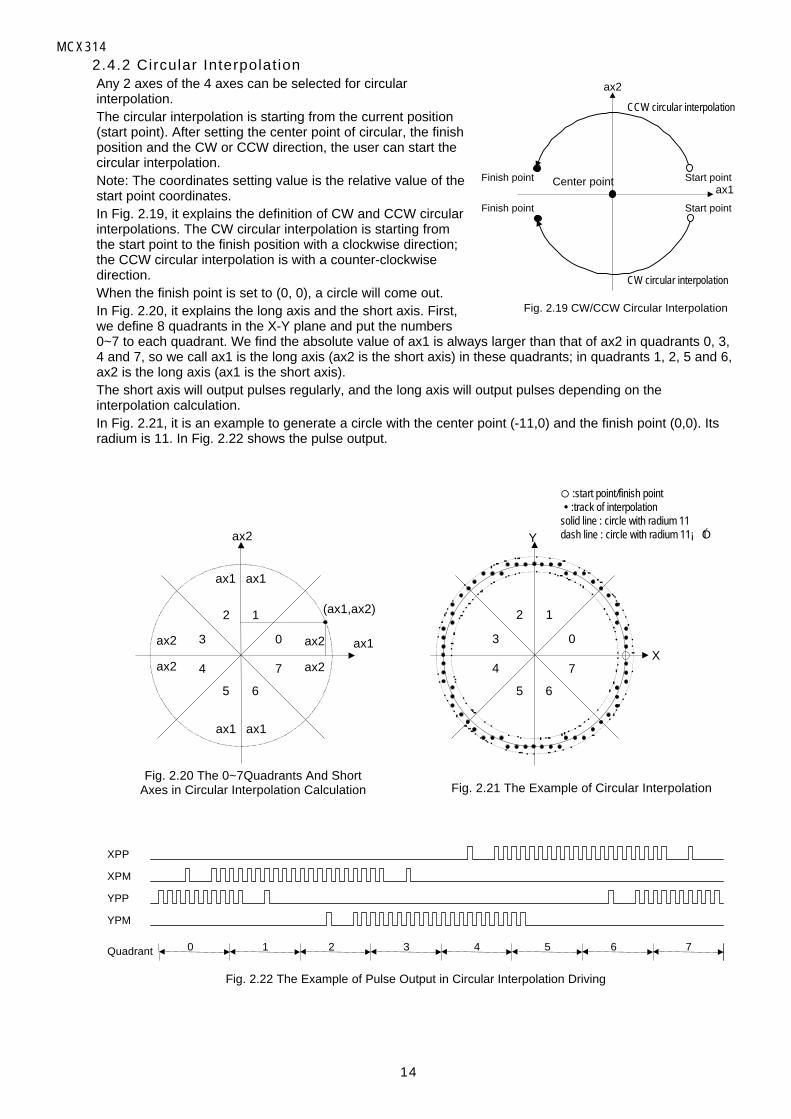
MCX314
14
2.4.2 Circular Interpolat ion Any 2 axes of the 4 axes can be selected for circularinterpolation. The circular interpolation is starting from the current position(start point). After setting the center point of circular, the finishposition and the CW or CCW direction, the user can start thecircular interpolation. Note: The coordinates setting value is the relative value of thestart point coordinates. In Fig. 2.19, it explains the definition of CW and CCW circularinterpolations. The CW circular interpolation is starting fromthe start point to the finish position with a clockwise direction;the CCW circular interpolation is with a counter-clockwisedirection. When the finish point is set to (0, 0), a circle will come out. In Fig. 2.20, it explains the long axis and the short axis. First,we define 8 quadrants in the X-Y plane and put the numbers0~7 to each quadrant. We find the absolute value of ax1 is always larger than that of ax2 in quadrants 0, 3,4 and 7, so we call ax1 is the long axis (ax2 is the short axis) in these quadrants; in quadrants 1, 2, 5 and 6,ax2 is the long axis (ax1 is the short axis). The short axis will output pulses regularly, and the long axis will output pulses depending on theinterpolation calculation. In Fig. 2.21, it is an example to generate a circle with the center point (-11,0) and the finish point (0,0). Itsradium is 11. In Fig. 2.22 shows the pulse output.
ax2
12
65
7
0
4
3 ax1
ax1ax1
ax1ax1
ax2
ax2
ax2
ax2
(ax1,ax2)
Fig. 2.20 The 0~7Quadrants And ShortAxes in Circular Interpolation Calculation
X
Y
12
65
7
0
4
3
Fig. 2.21 The Example of Circular Interpolation
¡ :start point/finish point :track of interpolation
solid line : circle with radium 11dash line : circle with radium 11¡Ó1
XPP
XPM
YPP
YPM
0 1 2 3 4 75 6Quadrant
Fig. 2.22 The Example of Pulse Output in Circular Interpolation Driving
ax2
ax1
Fig. 2.19 CW/CCW Circular Interpolation
Center pointFinish point
Finish point
Start point
Start point
CCW circular interpolation
CW circular interpolation

MCX314
15
¡ ½The Finish Point Checking of Circular Interpolation
In the circular interpolation, it assumes that the currentposition (start point) is (0,0). After the coordinates of thecenter point is set, the radium will be decided, and thecircular tracking will start. The maximum error range ofinterpolation is with in ¡ Ó1LSB.
Because of the ¡ Ó1LSB error range, the designated finishpoint may not on the circular track. The IC will make an in-position checking by the short axis. If the value of finishpoint is as same as that of short axis, this circularinterpolation is finished. Fig. 2.23 shows an example of CCW interpolation with thestart point (0,0), center point (-200,500) and finish point (-702, 299). The finish point is in quadrant 4, and ax2 is theshort axis in quadrant 4. So the interpolation is finishedwhen the ax2 is 299. The range of interpolation coordinate is from the startpoint to -8,388,608 ~ +8,388,607, and the interpolationerror for all the range is within¡ Ó1LSB. The speed ofinterpolation driving is 1PPS ~ 4MPPS.
¡ ½The Example for CW Circular Interpolation This CW circular interpolation starts from the current point (start point: 0, 0) to the finish point ( X: 5000, Y: -5000); the center point is X: 5000, Y: 0. The interpolating speed is constant at 1000PPS in a constant vectorspeed driving.
WR5 ← 0104h write ; define: ax1:X axis, ax2:Y axis, and with constant linear speed
WR6 ← 0900h write ; range : 4,000,000 (multiple: 2)WR7 ← 003Dh writeWR0 ← 0100h write
WR6 ← 4DC0h write ; range of constant vector speed for 2 axesWR7 ← 0056h write ; 4,000,000 x 1.414 = 5,656,000WR0 ← 0200h write
WR0 ← 01F4h write ; initial speed : 500 x 2 = 1000PPSWR0 ← 0104h write
WR6 ← 01F4h write ; drive speed : 500 x 2 = 1000PPSWR0 ← 0105h write
WR6 ← 1388h write ; center point of X :5,000WR7 ← 0000h writeWR0 ← 0108h write
WR6 ← 0000h write ; center point of Y :0WR7 ← 0000h writeWR0 ← 0208h write
WR6 ← 1388h write ; finish point of X :5,000WR7 ← 0000h writeWR0 ← 0106h write
WR6 ← EC78h write ; finish point of Y :-5,000WR7 ← FFFFh writeWR0 ← 0206h write
WR0 ← 0032h write ; CW circular interpolation enabling
Finish point (-720,299)
Start point (0,0)
Fig. 2.23 Example of In-position Check inCircular Interpolation
ax2
12
65
7
0
4
3ax1
Interpolation will be finished whenax2=299 in the 4th quadrant
Center point (-200,500)
Y
X
End point(5000,-5000)
Center point(5000,0)
Start point (0,0)
Fig. EX.2 CW Circular Interpolation inConstant Vector Speed

MCX314
16
2.4.3 The Bit Pattern Interpolat ion MCX314 is able to receive the interpolation data fromthe host CPU, and output pulses at a specific speed.The host CPU executes the interpolation for 2 or 3 axes,generates a set of pulse data, then writes thecommands into MCX314. MCX314 will output thepulses at a specific speed. Every axis has 2 bit-data buffers for host CPU: one for+ direction and the other for - direction. Whenperforming the bit pattern interpolation, the host CPUwill write the designated interpolation data, for 2 or 3axes, into MCX314. If a bit in the bit pattern data from CPU is “1” , MCX314will output a pulse at the time unit; if it is “0” , MCX314will not output any pulse at the time unit. For example, if the user want to generate the X-Y profile (see Fig. 2.24), the host CPU must write a set ofpattern into those specific registers ---- XPP: the + direction register for X axis, XPM: the - direction registerfor X axis, YPP and YPM: the + and - directions registers. With in the time unit, MCX314 will check theregisters once and decide to output a pulse or not depending on the bit pattern.
←56 ←48 ←40 ←32 ←24 ←16 ←8 ←0 01000000 00000000 00011111 11011011 11110110 11111110 00000000 00000000 : XPP (X + direction) 01111111 11110101 00000000 00000000 00000000 00000000 00101011 11111111 : XPM (X -direction ) 00000000 00000000 00000000 11111111 00000000 00001111 11111111 11010100 : YPP (Y + direction) 00001010 11111111 11111100 00000000 00111111 11000000 00000000 00000000 : YPM (Y - direction)
Fig. 2.25 is the block diagram of bit pattern interpolation for the 1st axis in MCX314. BP1P register and BP1M register are 16 bit-data buffers for bit pattern data form the host CPU. (IF thesystem uses 8-bit data bus, the host CPU has to write the data by low byte and high byte.) The + directiondata should be written into PB1P, and the - direction data into PB1M. Once starting the bit patterninterpolation, the pulse outputting is in the order from D0.
0 0 0 0 1 0 0 0 0 0 0 0 0 1 0 0
0 0 0 1 0 0 1 0 0 0 0 1 0 0 0 0
1 0 0 1 1 0 1 0 0 1 1 1 0 1 0 1
0 1 0 0 0 0 0 0 0 0 1 0 0 0 0 1
1 1 1 0 1 0 1
ax1-PP
SC=2REG2
REG1
SREG
D15 D0
1
0
BP1P
Sys. CPU
0 1 0 0 0 0 0 1 0 0 0 0 1 0 1 0
1 0 0 0 0 1 0 0 0 0 1 0 0 0 0 0
0 0 0 0 0 0 0 0 0 0 0 0 1 0 1 0
0 0 0 0 0 1 1 1 0 0 0 0 1 0 1 0
1 0 1 0
ax1-PM
SC=2REG2
REG1
SREG
D15 D0
1
0
BP1M
Sys. CPU
0~3
SC
SC: Stack counter (RR0/D14,13)BP1P: Data register (ax1 + direction)BP1M: Data register (ax1 - direction)SREG: 16 bit shift registerREG1: 16 bit buffer register 1REG2:16 bit buffer register 2
0 0 0
Fig. 2.25 The Structure of Register for The Bit Pattern Interpolation ( for 1 axis) Stacking counter (SC) is a 2-bit counter. Its value is between 0 and 3, which can be read from D14,13 ofregister RR0. SC will decide which register for the data from the host CPU. The initial value of SC is 0. So,
62
0
16
8
32
24
48
40
56
X
Fig. 2.24 Example for Bit Pattern Interpolation

MCX314
17
when host CPU writes bit pattern data into BP1P or BP1M, the data will be stored in SREG, and then, SCwill count up to 1, and the next data from the host CPU will be written into REG1. By this way, the REG2becomes the register when SC=2. The host CPU is not able to write any bit pattern data into MCX314 whenSC=3. When the bit pattern interpolation pulse is outputting, D0 in SREG will be shifted output first, and then in theorder of D1, D… When all of SREGs have been shifted output, the data in REG1 will be shifted to SREG,the data in REG2 will be shifted to REG1, and the SC will count down to 2. Then, the host CPU is able towrite a new data into MCX314 again. In order to make MCX314 output the bit pattern data continuously, the host CPU should write the data intoMCX314 before SC counts down to 0. MCX314 will output a interrupt requirement signal to host CPU whenSC counts down from 2 to 1.
¡ ½The limitation for the speed of bit pattern interpolation driving The maximum pulse output speed of MCX314 is 4MHz in bit pattern interpolation mode. However, themaximum speed will depend on the data update rate of host CPU if the bit pattern data are more than48bits. For example of the X and Y axes bit pattern interpolation, if the host CPU needs 100usec to updatenew 16-bit data for X and Y axes. The maximum speed is 16/100µSEC=160KPPS.
¡ ½The ending of bit pattern interpolation There are 2 ways can terminate the bit pattern interpolation. Write a ending code into buffer register of ax1.
The bit pattern interpolation mode will be finished, and stopped if the host CPU write “1” into both + and- directions buffer registers.
The Interpolation Stops Once The + And - Directions Are “1”.
0 0 0 0 0 1 1 1 1 0 1 0 0 0 0 0
D15 D0
0 0 0 0 0 1 0 0 0 0 0 0 1 1 1 1
BP1P
BP1M
When the ending code is executed, the SC will become 0 automatically. The host CPU stops writing any command into MCX314.
When SC=0, and when no other data is updated, MCX314 will stop outputting pulse. Then, the bit patterninterpolation is finished.
¡ ½Utilizing the stop command to pause the interpolation The interpolation driving will be paused if a sudden stop or decelerating stop command is written into themaster axis (ax1) which is executing the bit pattern interpolation. MCX314 will continue the bit patterninterpolation if the host CPU enables the bit pattern interpolation again. If the host CPU wants to finish theinterpolation after writing stop command, all of the interpolation bit data in MCX314 must be cleared inusing BP register (3Dh).
¡ ½Utilizing hardware limit to interrupt the interpolation The interpolation driving will be terminated when any hardware limit of any axis is active. And, if host CPUwants to finish the interpolation, all of the interpolation data in MCX314 must be cleared.

MCX314
18
¡ ½Writing the bit pattern data into the register in MCX314 Either by 16-bit data bus or by 8-bit data bus, the address map of the command buffer for bit patterninterpolation data is show as follows:
The addresses map of register for 16-bit data bus in bit pattern interpolation
Address
A2 A1 A0 Name of register Content The register with the
same address
0 0 0 WR0
0 0 1 nWR1
0 1 0 BP1P ax1 +direction data nWR2
0 1 1 BP1M ax1 -direction data nWR3
1 0 0 BP2P ax2 +direction data WR4
1 0 1 BP2M ax2 -direction data WR5
1 1 0 BP3P ax3 +direction data WR6
1 1 1 BP3M ax3 -direction data WR7
Note: BP3P and BP3M share the same registers: WR6 and 7. The addresses map of register for 8-bit data bus in bit pattern interpolation
Address Address
A3 A2 A1 A0 Name of register
A3 A2 A1 A0 Name of register
0 0 0 0 1 0 0 0 BP2PL
0 0 0 1 1 0 0 1 BP2PH
0 0 1 0 1 0 1 0 BP2ML
0 0 1 1 1 0 1 1 BP2MH
0 1 0 0 BP1PL 1 1 0 0 BP3PL
0 1 0 1 BP1PH 1 1 0 1 BP3PH
0 1 1 0 BP1ML 1 1 1 0 BP3ML
0 1 1 1 BP1MH 1 1 1 1 BP3MH
Note: BPmPL, BPmPH, BPmML, BPmMH represent the following bit groups (m is 1 ~ 3 ). BPmPL : the low byte of BPmP (D7 ~ D0) BPmPH : the high byte of BPmP (D15 ~ D8) BPmML : the low byte of BPmM (D7 ~ D0) BPmMH : the high byte of BPmM (D15 ~ D8)
For some addresses of bit pattern data registers are as same as nWR2 ~ nWR7, the host CPU can notwrite any data into the bit pattern data register since MCX314 has been reset. To write the bit patterncommand, the host CPU should be with the following sequence.
Write bit pattern(BP) enable command(36h) into command register
↓
Write bit pattern data
↓
Write BP disable command(37h) into command register Note : If the host CPU doesn’ t disable the BP data register, the data in nWR2 ~ nWR5 registers cannot be assessed. ¡ ½The example of bit pattern interpolation The bit interpolation example is shown in Fig. 2.24. We set X axis as ax1, Y axis as ax2 and a constant

MCX314
19
speed: 1000PPS in a constant vector speed interpolation driving.WR5 ← 0104h write ;Define ax1: X , ax2:YWR6 ← 0900h write ;setting the master axis speed
parameterWR7 ← 003Dh write ;range: 4,000,000 (multiple rate:2)WR0 ← 0100h write
WR6 ← 4DC0h write ;range of constant line speedWR7 ← 0056h write ;4,000,000x1.414=5,656,000WR0 ← 0200h write
WR6 ← 01F4h write ;Initial speed:500x2=1000PPSWR0 ← 0104h write
WR6 ← 01F4h write ;drive speed: 500x2=1000PPSWR0 ← 0105h write
WR0 ← 0039h write ;clear BP data
WR0 ← 0036h write ;enable to write into BP register
; command of bit 0~15th
BP1P ← 0000h write ;X axis +direction commandBP1M ← 2BFFh write ;X axis –direction commandBP2P ← FFD4h write ;Y axis +direction commandBP2M ← 0000h write ;Y axis –direction commandWR0 ← 0038h write ;BP data stacking, SC=1
; command of bit 16~31th
BP1P ← F6FEhwrite ;X axis +direction commandBP1M ← 0000h write ;X axis –direction commandBP2P ← 000Fh write ;Y axis +direction command
BP2M ← 3FC0h write ;Y axis –direction commandWR0 ← 0038h write ;BP data stacking, SC=2
; command of bit 32~47th
BP1P ← 1FDBh write ;X axis +direction commandBP1M ← 0000h write ;X axis –direction commandBP2P ← 00FFh write ;Y axis +direction commandBP2M ← FC00h write ;Y axis –direction commandWR0 ← 0038h write ;BP data stacking, SC=3
WR0 ← 0034h write ;enable 2 axis bit pattern;interpolation, because SC=3
J1 RR0/D14,13 read ;until the SC is less than 2If D14=D13=1 Jump to J1
; command of bit 48~63th
BP1P ← 4000h write ;X axis +direction commandBP1M ← 7FF5h write ;X axis –direction commandBP2P ← 0000h write ;Y axis +direction commandBP2M ← 0AFFh write ;Y axis –direction commandWR0 ← 0038h write ;BP data stacking, SC=3
WR0 ← 0037h write ;disable to write into BP register
J2 RR0/D8 read ;until ending interpolation driveIf D8=1 Jump to J2
(Note 1: If there is more BP data coming then repeat this process)
¡ ½Executing bit pattern interpolation by interrupt During the bit pattern interpolation, MCX314 will generate an interrupt request signal to the host CPU whileSC changes the value from 2 to 1. To enable the interrupt, the host CPU must set D15 of register WR5 to 1.Then, INTN of MCX314 will go low once SC changes the value from 2 to 1. The host CPU will check the SCvalue, and write bit pattern command into the register. The interrupt signal will be released if the host CPUwrites the SC stacking command(38h) into MCX314. The interrupt signal will be released when the clearcommand(3dh) is written into the command register. If the interrupt status is keeping on the Low level, it will return to high-Z level after MCX314 finishes the bitpattern interpolation.
2.4.4 Constant Vector Speed MCX314 is with the constant vector speed control function whichcan control the resultant speed of two axes to keep the speed inconstant. Fig. 2.26 shows the profile of 2 axes interpolation driving. Thevector speed reflects 1.414 times of the individual axis drivingspeed. So, we have to set the speed of 1.414 times to keep thevector speed for 2-axis driving.
¡ ½Constant Vector Speed Set-up The user should first set the values of D9 and D8 of registerWR5to 0 and 1.Then, set the range R of salve-axis (ax2) to be 1.414 times of the value of the master-axis(ax1). Therefore, MCX314 will use the range parameter of master-axis if only 1 axis outputs pulses.However, when 2 axes output pulses simultaneously, MCX314 will use the range parameter of slave-axis toimplement the pulse period to 1.414 times.
¡ ½The Example of Constant Vector Speed Interpolation for 2 Axes As shown below, the master-axis (ax1) = X axis, the slave-axis (ax2) = Y axis, and the interpolation is at aconstant vector speed: 1000PPS. The result of driving pulse output is shown in Fig. 2.27.
X
Y
Fig. 2.26 Example of 2 axis interpolation
Not
e1

MCX314
20
WR5 ← 0104h write ; define ax1: X axis, ax2:Y axis
; constant vector speed
WR6 ← 0900h write ; setting parameter of the master axisWR7 ← 003Dh write ; range: 4,000,000 (multiple=2)WR0 ← 0100h write
WR6 ← 4DC0h write ; range of 2-axis constant vector speedWR7 ← 0056h write ; 4,000,000x1.414=5,656,000WR0 ← 0200h write
WR6 ← 01F4h write ; initial speed: 500x2=1000PPSWR0 ← 0104h write
WR6 ← 01F4h write ; drive speed: 500x2=1000PPS
WR0 ← 0105h write
WR6 ← 03E8h write ; finish point of X WR7 ← 0000h write WR0 ← 0106h write ;
WR6 ← 0190h write ; finish point of Y
WR7 ← 0000h write WR0 ← 0206h write ;
WR0 ← 0030h write ; 2-axis linear interpolation starting
XPP
XPM
YPP
YPM
1.000ms 1.414ms 1.000ms 1.414ms
Fig. 2.27 The Example of 2-axis Interpolation at A Constant Vector Speed (speed=1000PPS)
¡ ½Setting Constant Vector Speed for 3 Axes As same as the setting process of 2 axes, the user should first set the values of D9 and D8 of register WR5to 0 and 1. Then, set the range R of ax2 to 1.414 times of the value of the master-axis (ax1); then, set therange R of ax3 to 1.732 times of the value of the master axis. After setting the range of constant vector speed for 3 axes, MCX314 will use the range parameter of ax1 ifonly 1 axis outputs pulses. However, when 2 or 3 axes output pulses simultaneously, MCX314 will use therange parameter of ax2 or ax3 to implement the pulse period. See Fig. 2.28. User may set the values of D9 and D8 of register WR5 to 0 and 1 for 2-axis constant vector speed drivingeven in the 3-axis interpolation.
XPP
XPM
YPP
YPM
1.000ms 1.414ms 1.000ms 1.732ms 1.414ms
ZPP
ZPM
Fig. 2.28 Example for 3-axis Interpolation at A Constant Vector Speed (speed=1000PPS)
Caution: In the process of constant vector speed, the pulse width of high level of output waveform will notbe changed, yet kept in the same width. The pulse cycle will be changed to 1.414 or 1.732 times.

MCX314
21
2.4.5 Continuous Interpolat ion The continuous interpolation is executing a series ofinterpolation processes such as linear interpolation ¡ ÷circularinterpolation¡ ÷linear interpolation … During the continuousinterpolation, the driving will not stop; contrarily, The pulses areoutputcontinuously. When executing the continuous interpolation, the host CPU hasto write the next interpolation command into MCX314 before theprevious interpolation command is finished.
¡ ½Continuous Interpolation in Using D9 of RR0 If D9 (CNEXT) of register RR0 is 1, MCX314 is ready to acceptthe next interpolation command. If D9 is 0, the host CPU is notable to write the next interpolation command into MCX314. The D9 will become 1 only when the present command isexecuted. MCX314 will not accept the next command, and theD9 is 0 if the present command has not been executed. So, the standard procedure of continuous interpolation is first towrite, and enable the interpolation data and command, thencheck if D9 of RR0 is 1 or 0. And then, repeat writing commandsand checking D9. The flow chart is shown at the right side.
¡ ½Interrupt D14 of register WR5 is used for enable or disable the interruptduring the continuous interpolation. After setting D14 of registerWR5 to 1, the interrupt occurs. Pin INTN of MCX314 will be onthe Low level to interrupt the host CPU when D9 of register RR0become 1. The INTN will be on the Hi level if the host CPUwrites the next interpolation command to MCX314. If the interrupt clear command (3Dh) is written to commandregister, the INTN signal will return to high-Z level from the Lowlevel. During the ending of the interpolation, it is forced to be “ interruptdisable” , and the INTN signal will return to the high-Z level.
¡ ½Errors Occurring in the Process of Continuous Interpolation If an error such as over-traveling occurs in the process of continuous interpolation, the drive will stop at thepresent interpolation node. The following interpolation command is still in the command register, but will notbe executed. The host CPU has to reload the next command again and enable it. As shown in the flow chart above, the host CPU has to check the error message before loading thefollowing command. If not, this command will not be executed and will be jumped. So, the user shouldassure, and check if any error status will occur before the following interpolation command is loaded.
¡ ½Attentions for Continuous Interpolationl Before setting the interpolation command, the user should first set other data such as center point, finish
point… for each node.l The maximum speed for the continuous interpolation is 2MHz.l The following interpolation command must be loaded before the previous interpolation command is
finished.l The node driving time should be longer than the time for error checking and the command setting of
next node during the interpolation.l It is impossible to operate 2-axis and 3-axis continuous interpolations at the same time.l It is not allowed to change the axis assignment during the process of continuous interpolation.
The 1st nodedata write in
interpolation cmd. write in
errors occurred?
allow to write inthe next data?RR0/D9=1?
no
yes
The 2nd nodedata write in
interpolation cmd. write in
errors occurred?
allow to write inthe next data?RR0/D9=1?
no
yes
The 3rd nodedata write in
interpolation cmd. write in
Ending theinterpolation driveProcessing the errors

MCX314
22
¡ ½The Example of Continuous Interpolation Fig. 2.29 shows an example of executing continuous interpolation beginning at point (0,0) from node 1, 2,3….to the node 8. In node 1, 3, 5, and 7, the linear interpolation will be executed; in node 2, 4, 6, and 8, thecircular interpolation will be executed, and the track is a quadrant circle with radius 1500. The interpolationdriving is at a constant vector speed: 1000PPS.
WR5 ← 0104h write ; define ax1: X axis , ax2: Y axis, constant vector speed
WR6 ← 0900h write ; setting the parameter of master axisWR7 ← 003Dh write ; range:4,000,000 (multiple: 2)WR0 ← 0100h write
WR6 ← 4DC0h write ; 2-axis constant vector speedWR7 ← 0056h write ; 4,000,000x1.414=5,656,000WR0 ← 0200h write
WR6 ← 01F4h write ; Initial speed: 500x2=1000PPSWR0 ← 0104h write
WR6 ← 01F4h write ; drive speed: 500x2=1000PPSWR0 ← 0105h write
WR6 ← 1194h write ; finish point X: 4500WR7 ← 0000h writeWR0 ← 0106h write
WR6 ← 0000h write ; finish point Y: 0WR7 ← 0000h writeWR0 ← 0206h write
WR0 ← 0030h write ; 2-axis linear interpolation enabling
J1 RR0(D4, D5) read ; if error occursIf D4 or D5=1 Jump to Error; jump to handle error
RR0(D9) read ; waiting for next node’ s enable signalIf D9=0 Jump to J1 ;
WR6 ← 0000h write ; center X: 0WR7 ← 0000h writeWR0 ← 0108h write
WR6 ← 05DCh write ; center Y: 1500WR7 ← 0000h writeWR0 ← 0208h write
WR6 ← 05DCh write ; finish point X:1500WR7 ← 0000h writeWR0 ← 0106h write
WR6 ← 05DCh write ; finish point Y:1500WR7 ← 0000h writeWR0 ← 0206h write
WR0 ← 0033h write ; CCW circular interpolation enabling
Procedure A
WR6 ← 0000h write ; finish point X: 0WR7 ← 0000h writeWR0 ← 0106h write
WR6 ← 05DCh write ; finish point Y: 1500WR7 ← 0000h writeWR0 ← 0206h write
WR0 ← 0030h write ; 2-axis linear interpolation enabling
Procedure A
… …
1500
3000
4500
node5
node1node2
node3
node4
node8
node7
node6
60004500-1500 (0,0)
Node3
Node2
Node1
A

MCX314
23
(same procedure for nodes 4 ~ 8.)

MCX314
24
2.4.6 The Accelerat ion / Decelerat ion Control in Interpolat ion Different from other IC chips only allowing constant speed for executing the interpolations, MCX314supports the user to use trapezoidal and S-curve driving ( for linear interpolation only ). In the process of interpolation, for executing acceleration / deceleration in continuous interpolation process,the user can enable the deceleration by command (3Bh), or disable deceleration by command (3Ch). Thepurpose for the deceleration command is to enable the automatic deceleration or manual decelerationfunction; the purpose of the disable deceleration command is to disable both of them. It will be disable whilepower-on reset. During the driving, the deceleration enable command cannot be executed.
¡ ½The Acceleration / Deceleration for 2-axis / 3-axis Interpolation It is possible to perform trapezoidal and S-curve acceleration/deceleration driving during the execution of2-axis / 3-axis linear interpolation. Either automatic or manual deceleration can be used for decelerating. When the manual deceleration is executed, the user can set the maximum absolute value of the axes to bethe setting value of master axis decelerating point. For instance, while executing 3-axis linear interpolationof master axis (ax1): X, ax2 : Y and ax3 : Z, the finish point : (X: -20000, Y: 30000, Z: -50000), and theassumed pulse numbers needed for deceleration are 5000. In such situation, the absolute value of Z axis isthe largest, so we can set up 50000-5000=45000 to be the manual deceleration point of the master axis: X.
Please refer to the example of 3-axis linear interpolation in 2.4.1.

MCX314
25
¡ ½The Acceleration / Deceleration for Circular Interpolation and Bit Pattern Interpolation In circular interpolation and bit pattern interpolation, only manualdeceleration in trapezoidal driving is available; the automaticdeceleration in S-curve driving is not available. The Figure on the right side shows the circular interpolation of a realcircle with radius 1000 in a trapezoidal driving. The user shouldcalculate the decelerating point before driving because the automaticdeceleration will not be active. In the figure, the circle tracks through all the 8 quadrants: 0~7. Inquadrant 0, Y axis is the short axis and it’ s displace is about
10000 / ¡ Ô2=7071
The total output pulses numbers of the short axis are 7010x8=56568. Furthermore, if the initial speed is 500PPS, and will be acceleratedto 20KPPS after 0.3 SEC, the acceleration will be (20000-500) /0.3 =65000PPS/SEC. And the output pulses during acceleration will be(500+20000) x 0.3/2=3075. Thus, if we set the deceleration as sameas the acceleration, the manual decelerating point will be 56568-3075=53493. Note: this formula cannot be used in the constant vector speeddriving.
WR3 ← 0001hwrite ; manual deceleration enabling
WR5 ← 0004hwrite ; define ax1: X , ax2: Y
WR6 ← 8480hwrite ; range: 2,000,000; (multiple: 4)WR7 ← 001Eh write ;WR0 ← 0100hwrite
WR6 ← 0082hwrite ; acceleration :WR0 ← 0102hwrite ; 130x125x4=65000 PPS/SEC
WR6 ← 007Dh write ; Initial speed:125x4=500PPSWR0 ← 0104hwrite
WR6 ← 1388hwrite ; drive speed: 5000x4=20000PPSWR0 ← 0105hwrite
WR6 ← D8F0h write ; center point X : -10000WR7 ← FFFFh write ;WR0 ← 0108hwrite
WR6 ← 0000hwrite ; center point Y : 0WR7 ← 0000hwrite ;WR0 ← 0208hwrite
WR6 ← 0000hwrite ; finish point X : 0WR7 ← 0000hwrite ;WR0 ← 0106hwrite
WR6 ← 0000hwrite ; finish point Y : 0WR7 ← 0000hwrite ;WR0 ← 0206hwrite
WR6 ← D0F5h write ; manual deceleration point setting : 53493WR7 ← 0000hwrite ;WR0 ← 0107hwrite
WR0 ← 003Bh write ; deceleration enabling
WR0 ← 0033hwrite ; CCW circular interpolation starting
Y12
65
7
0
4
3
X
10000 7071
Short Axis
Output Pulse DuringAcceleration
0.3 Time(sec)
500
PPS
20k
Speed

MCX314
26
¡ ½The Acceleration / Deceleration for Continuous Interpolation In continuous interpolation, same as in circular and bit pattern interpolations, only manual deceleration inthe trapezoidal driving is available; The automatic deceleration in S-curve driving is not available. Before performing the continuous interpolation, it is necessary to preset the manual decelerating point;however, this setting point is related to the master axis executing the deceleration in the last node. The usershould disable the deceleration, then start the interpolation driving. Before writing the interpolationcommand to the final node which will execute the deceleration, the user should enable the deceleration atfirst. The deceleration will start if the output pulses are larger than the master axis based pulses in the finalnode. For instance, there are 5 interpolation nodes in the process of continuous interpolation. In case, the manualdeceleration has to be executed in the last node, node 5, the procedure is shown as follows:
Setting mode, acceleration / deceleration for master axis
↓
Writing manual deceleration point
↓
Deceleration disabling (command: 3Ch)
↓
Writing node 1 data, interpolation command
↓
Error checking, waiting for the allowance to write the next data
↓
Writing node 2 data, interpolation command
...
Error checking, waiting for the allowance to write in the next data
↓
Deceleration enabling (command: 3Bh)
↓
Writing node 5 data, interpolation command ¡ The manual deceleration point is related to the master axis’ driving pulses which comes from node 5.
For instance, assumed that it needs 2000 pulses for decelerating stop, and the total amount of pulseoutput form node 5 is 5000. So, the manual deceleration point will be 5000 - 2000 = 3000.
¡ The cycle of deceleration should be started and finished within the same node.
:Starting continuous interpolation driving

MCX314
27
2.4.6 Single-step interpolat ion (from Command or External Signal)
Single-step is defined as: pulse by pulse outputting. Either command or external signal can execute thesingle-step interpolation. When one pulse is outputting, the master axis interpolation will be set in theconstant speed driving. The Hi level width of each axis’ s output pulse is 1/2 of the pulse cycle which isdecided by the interpolating master axis’ s drive speed. The Low level width is kept until next command orexternal signal comes.Fig. 2.30 is the example showing the execution of single-step interpolation from an external signal. Themaster axis’ s initial speed is 500PPS, the drive speed is at 500PPS constant speed driving. The Hi levelwidth of output pulse is 1msec.
XPP
ExPLSN
YPM
1 mSEC
Fig. 2.30 Example of single step interpolation (500PPS) by external signal(EXPLSN)
¡ ½Command Controlled Single-step InterpolationThe command: 3Ah is for single-step interpolation. The user can set D12 of register WR5 to 1 to enable thecommand controlled single-step interpolation. The operating procedure is shown as follow. Set D12 of register WR5 to 1.
It will enable the command controlled single-step interpolation.
Set the initial and drive speeds of the master axis in the interpolation process with the same value, andthe driving becomes constant speed. If the host CPU writes single step command into MCX314 at most 1mSEC, the user should set the drive speed more than 1000PPS.
Set interpolation data. (start point, center point…)
Write interpolation command.Although the interpolation command is enabled, there is no pulse output because the single-step iscommand controlled.
Write the single-step interpolation command (3Ah).The driving pulses according to the interpolation calculation will be output for each axis. The user mayuse command 3Ah for single step until the interpolation driving is finished.
If the user wants to stop sending single-steps during the interpolation, he can use the sudden stopcommand (27h), then wait for more than 1 pulse cycle, and then write the command (3Ah) again to stopthe driving. After this, all the following (3Ah) commands will not be active.
¡ ½External Signal Controlled Single-step InterpolationThe EXPLSN pin ( 29) is used for the single-step interpolation from the external signal. The user can setD11 of register WR5 to 1 to enable the external signal controlled single-step interpolation. Normally, theEXPLSN input signal is on the Hi level. When it changes to Low, the interpolation step will be output. Theoperating procedure is shown as follows. Set D11 of register WR5 to 1.
It will enable the external signal controlled single-step interpolation.
Set the initial and driving speeds of the master axis in the interpolation process to be the same value,and the driving becomes constant speed which should be higher than the Low pulse cycle of EXPLSN.This is necessary for this controlled mode. And it will set the MCX314 into a constant speed mode.
Set interpolation data. (starting point, center point…)
Write interpolation command.Although the interpolation command is enabled, there is no pulse output because the single-step iscommand controlled.
EXPLSN input on Low levelThe interpolation pulse will be output from each axis after 2~5 CLK the pulse falling down. The Low levelpulse width of EXPLSN has to be longer than 4CLK. Furthermore, the pulse cycle of EXPLSN has to belonger than the setting speed cycle of master axis. The user may repeat the Low level of EXPLSN beforethe interpolation is finished.

MCX314
28
If the user wants to stop sending single-steps during the interpolation, he can use the sudden stopcommand (27h), then wait for more than 1 pulse cycle, and then input pulse on EXPLSN Low level againto stop the driving (the user may try software reset also). After this, all the following input pulses onEXPLSN Low level will not be active.
Note: When connecting the EXPLSN Low level with the manual connector, please assure the EXPLSNsignal is not chattering.
2.5 Interrupt
The interrupt is generated from X, Y, Z, or U axis, bit pattern interpolation or continuous interpolation.There is only one interrupt signal, INTN (33), to the host CPU. So, the signal will be OR calculated, thenoutput, as shown in Fig. 2.31.
INTN(33)
X Axis
INT
YAxis
INT
Z Axis
INT
U Axis
INT INT
Interpolationcontrol unit
Figure 2.31 Interrupt Signal Path in IC
Every interrupt can be enabled or disabled individually. During the power resetting, all interrupt signals aredisabled.
n Interrupt of X, Y, Z, and U AxesThe following table shows the interrupt factors generated by X, Y, Z, and U axes.
Enable / DisablenWR1 Register
StatusnRR3 Register
The Factors of Interrupt Happening
D8(PULSE) D0(PULSE) when one pulse outputs... (The interrupt will be generated at therising edge of pulse output for + direction driving.)
D9(P≥C-) D1(P≥C-) once the value of logical / real position counter is larger than or equalto the value of COMP- register (CM)...
D10(P<C-) D2(P<C-) once the value of logical/real position counter is smaller than thevalue of COMP- register (CM)...
D11(P<C+) D3(P<C+) once the value of logical / real position counter is larger than thevalue of COMP+ register (CM)…
D12(P≥C+) D4(P≥C+) once the value of logical / real position counter is smaller than orequal to the value of COMP+ register (CM)...
D13(C-END) D5(C-END) in the acceleration / deceleration driving, when the driving changesfrom the constant speed region into the decelerating region...
D14(C-STA) D6(C-STA) in the acceleration / deceleration driving, when the driving changesfrom the accelerating region into the constant speed region…
D15(D-END) D7(D-END) when the driving is finished...
Each factor of interrupt can be masked by setting levels in nWR1 register bits: 1- enable and 0 - disable.When interrupt is generated during the driving, and if the interrupt is generated, each bit in nRR3 will be setto 1; INTN will be on the Low level. After the nRR3 status has been read from the host CPU, nRR3 will becleared from 1 to 0, and INTN will return to the High-Z level.

MCX314
29
nInterrupt from InterpolationsEnable / DisableWR5 Register
Status CheckRR0 Register
The Factors of Interrupt Happening*Interrupt Clearing
D14(CIINT) D9(CNEXT)
in continuous interpolation, when MCX314 is available for theinterpolation data of next node...*after next interpolation command is written, the interrupt will becleared.
D15(BPINT) D14,13(BPS1,0)
In bit pattern interpolation, when the value of stack connector (SC) ischanged from 2 to 1, and the stack is available for next BP commandwriting...*after a BP command for the stack is written, the interrupt will becleared.
When an interrupt is generated during interpolations, this interrupt can be cleared by writing the interruptclear command (3Dh) INTN will return to the High-Z level automatically once the interpolation is finished.
2.6 Other Functions
2.6.1 Driving By External PulsesFixed pulse driving and continuous pulse driving can be controlled by either commands or external signals,which can reduce the load of host CPU.Each axis has two input signals, nEXPP and nEXPM. nEXPP controls + direction pulse output, and nEXPMcontrols – direction command. D3 and D4 bits of register WR3 are for the setting in driving. The user shouldpreset the parameters and commands. The default level of nEXPP and nEXPM is normally set on Hi.
nFixed Pulse Driving ModeSet bits D4 and D3 of register WR3 to 1 and 0 respectively, and set all the parameters of fixed pulse driving.Once nEXPP is falling down to the Low level (¡ õ), the + direction fixed pulse driving will start; once nEXPPis raising to the Hi level (¡ ô), the - direction fixed pulse driving will start. The width of Low level signal mustbe larger than 4 CLK-cycle. Before this driving is finished, a new Hi-to-Low level falling down of the signal isinvalid.
XEXPP
XEXPM
XPP
XPM
Fig. 2.32 Example of The Fixed Pulse Driving by External Signal
[Note] When connecting the input signal with a mechanical connector, the signal chattering would happen,especially if the output pulse numbers are few. Please add a de-bounce circuit to avoid the chattering.
nContinuous Pulse Driving ModeSet bits D4 and D3 of WR3 register to be 1 and 0 respectively, and set all the parameters of continuouspulse driving. Once nEXPP is falling down to the Low level (¡ õ), the + direction continuous pulse drivingwill start; once nEXPP is raising to the Hi level (¡ ô), the - direction fixed pulse driving will start. WhennEXPP returns to the Hi level from the Low level, the decelerating stop will be performed in trapezoidaldriving, and the sudden stop in constant speed driving.
XEXPP
XEXPM
XPP
XPM
Low period
Low period
Figure 2.33 Example of Continuous Driving by External Signal

MCX314
30
2.6.2 Pulse Output Type Select ionThere are two types of pulse output--independent 2-pulse type: when the driving is in + direction, the pulseoutput is from nPP/PLS; when the driving is in - direction, the pulse output is from nPM/DIR; 1-pulse 1-direction type: nPP/PLS is for pulse outputting, and nPM/DIR is for direction signal outputting. (pulse / direction is set on the positive logical level)
Pulse Output WaveformPulse Output Type Drive Direction
nPP/PLS Signal NPM/DIR Signal
+Direction Low levelIndependent 2-pulse
- Direction Low level
+Direction Low level1-pulse 1-direction
- Direction Hi level
Bit D6 (PLSMD) of register WR2 is used for the selection of pulse output type.Additionally, bits D7 (PLS-L) and D8 (DIR-L) of register WR2can be used for pulse outputting, direction andlogical level setting.
[Note] Please refer to Chapter 13.2 and 13.3 for the pulse signal (nPLS) and direction signal (nDIR) in 1-pulse 1-direction pulse outputting.
2.6.3 Pulse Input Type Select ionFor real position counter, A/B quadrature pulse type and Up / Down pulse type can be selected for pulseinput. When A/B quadrature pulse type is selected, the position counter will count up if phase A leadsphase B; the position counter will count down if phase B leads phase A. The pulse cycle can be set 1/2 or1/4.
nECA/ PPIN
nECB/ PMIN
Counting Up Counting Down
When Up / Down pulse type is selected, nECA/PPIN is used for count-up input, and ECB/PPIN for count-down input. The counting is during the + direction pulses are up (¡ ô).
nECA/ PPIN
nECB/ PMIN
Counting Up Counting Down
2.6.4 Hardware Limit SignalsHardware limit signals, nLMTP and nLMTM, are used for stopping the pulse output if the limit sensors of +and - directions are triggered. When the limit signal and also the logical level are active, the command ofsudden stop or decelerating stop can be set by bits D3 and D4 (HLMT+, HLMT-), and D2 (LMTMD) ofregister WR2.

MCX314
31
2.6.5 Interface to Servo Motor DriversEnable / Disable and logical levels of the input signals for connecting servo motor drivers such as nINPOS(in-position input signal) and nALARM (alarm input signal) can be set by D15~12 bits of register WR2.nINPOS input signal responds to the in-position signal of servo motor driver. When “enable” is set, andwhen the driving is finished, nINPOS will wait for the “active” . Then, the n-DRV bit of main status registerPRO will return to 0.nALARM input signal receives the alarm signal from servo motor drivers. When “enable” is set, nALARMsignal will be monitored, and the D4 (alarm) bit of RR2 register is 1 when nALARM is active. The suddenstop will occur in the driving when this signal is active.These input signals from servo motor drivers can be read by RR5 and RR6 registersThe user can use general output signals nOUT7~4 or nOUT3~0 to clear and/or reset the out put signalssuch as deviation counter and alarm reset of servo motor drivers.
2.6.6 Emergency StopSignal EMGN is able to perform the emergency stop function for all of the 4 axes during the driving.Normally, this signal is kept on the Hi level. When it is falling to the Low level, all axes will stop immediately,and the D5 (EMG) bit of register RR2 (each axis) becomes 1. Please be noted that there is no way to selectthe logical level of EMGN signal.Please check the following methods to perform the emergency stop function from the host CPU.¬ Execute the sudden stop commend for all of the 4 axes at the same time…
Appoint all of the 4 axes, then write the sudden stop command (27h) to register WR0. Reset software limit…
Write 800h to register WR0 to reset software limit.
2.6.7 Status Output
nDRIVE output signals and bits D3~0 (n-DRV) of registerRR0 can be used for drive / stop status output of each axis.The driving status of acceleration / constant speed /deceleration will be output to bits D2 (ASND), D3 (CNST)and D4 (DSDN), and also the signals nOUT6 / ASND andnOUT7 / DSND will show the levels. However, these outputsignals and general purpose output signals share the sameterminal, D7 (OUTSL) bit of register WR3 should be set 1for drive status output.
Status Register Output SignalDrive Status RR0/n-DRV nRR1/ASN
DnRR1/CNS
TnRR1/DSN
DnDRIVE nOUT6/AS
NDnOUT7/DS
NDStop 0 0 0 0 Low Low Low
Acceleration 1 1 0 0 Hi Hi LowConstant Speed 1 0 1 0 Hi Low Low
Deceleration 1 0 0 1 Hi Low HiMoreover, in S-curve accelerating/decelerating driving, the state of acceleration /constant speed/deceleration will be also shown to bits D5 (AASND), D6 (ACNST), and D7 (ADSND) of register RR1.
2.6.8 General Purpose OutputIn MCX314, there are 8 general purpose output pins, nOUT3~0 & nOUT7~4, for each axis. However, duringthe outputting, nOUT7~4 cannot be used cause they share the same terminals with the position comparisonoutput and drive status output. NOUT3~0 can be output when the output levels of register WR4 have beenset. If the user wants to use nOUT7~4 signals, D7(OUTSL) of register WR3 should be set in the “generalpurpose output mode” , then the output levels of D11~8(OUT7~4) of register WR3 can be set for outputting.It is possible to use the general purpose output signal for motor driver current-OFF, deviation counting clearand alarm reset…When resetting, each bit of WR4 and nWR3 registers will be cleared, then, their output levels will be kept
Speed
Time
Acceleration DecelerationConstant speed StopStop

MCX314
32
on the Low level.

MCX314
33
3. Pin Assignments and Signal Description
XOUT4/CMPP60XOUT5/CMPM59XOUT6/ASND58XOUT7/DSND57XDRIVE56GND55VDD54CLK53
XALARM68XINPOS67GMD66VDD65XOUT064XOUT163XOUT262XOUT361
XECA/PPIN44UPM/DIR43UPP/PLS42ZPM/DIR41ZPP/PLS40YPM/DIR39YPP/PLS38GND37
GND52UECB/PMIN51UECA/PPIN50ZECB/PMIN49ZECA/PPIN48YECB/PMIN47YECA/PPIN46XECB/PMIN45
XIN272XIN371XLMTM70XLMTP69
UIN0 121UDRIVE 122
UOUT7/DSND 123UOUT6/ASND 124UOUT5/CMPM 125
VDD 126GND 127
UOUT4/CMPP 128
ZOUT0 113UINPOS 114
UALARM 115ULMTP 116ULMTM 117
UIN3 118UIN2 119UIN1 120
YEXPM 137ZEXPP 138ZEXPM 139UEXPP 140UEXPM 141
EMGN 142GND 143VDD 144
UOUT3 129UOUT2 130UOUT1 131UOUT0 132
GND 133XEXPP 134XEXPM 135YEXPP 136
VDD 109ZOUT3 110ZOUT2 111ZOUT1 112
YIN
PO
SY
ALA
RM
YLM
TP
YLM
TM
YIN
3V
DD
GN
DY
IN2
YO
UT
7/D
SN
DY
OU
T6/
AS
ND
YO
UT
5/C
MP
MY
OU
T4/
CM
PP
YO
UT
3Y
OU
T2
YO
UT
1Y
OU
T0
ZIN
1Z
IN0
GN
DZ
DR
IVE
ZO
UT
7/D
SN
DZ
OU
T6/
AS
DN
ZO
UT
5/C
MP
MZ
OU
T4/
CM
PP
YIN
1Y
IN0
ZIN
PO
SZ
ALA
RM
ZLM
TP
ZLM
TM
ZIN
3Z
IN2
XIN
1X
IN0
GN
DY
DR
IVE
8586878889909192 7778798081828384101
102
103
104
105
106
107
108
93949596979899100
73747576
A0
24A
123
A2
22A
321
GN
D20
GN
D19
VD
D18
D0
17
BU
SY
N32
TE
ST
N31
H16
L830
EX
PLS
N29
RE
SE
TN
28R
DN
27W
RN
26C
SN
25
D8
8D
97
D10
6D
115
D12
4D
133
D14
2D
151
D1
16D
215
D3
14D
413
D5
12D
611
D7
10G
ND
9
XP
M/D
IR36
XP
P/P
LS35
SC
LK34
INT
N33
Pin 1 Mask
NOVA elec.MCX314
144pinQFP, Dimension: 30.9x30.9 mm, Pitch: 0.65mm

MCX314
34
n Signal DescriptionSignals XOOO, YOOO, ZOOO, and UOOO are input / output signals for X, Y, Z, and U axes, where nstands for X, Y, Z, and U. If the signals are named OOON, they are negative-active or low-active.
Signal Name Pin No.Input
/OutputSignal Description
CLK 53 Input A Clock: clock signal for internal synchronous loop of MCX314The standard frequency is 16 MHz. This signal is for drive speed,acceleration / deceleration and jerk. If the frequency setting is not 16 MHz,the setting values of speed and acceleration / deceleration are different.
D15-D0 1~8,
10~17
Bi-directional A
DATA BUS: 3-state bi-direction 16-bit data busWhen CSN=Low and RDN=Low, these signals are for outputting. Otherwise,they are high impedance inputs. If 8-bit data bus is used, D15-D8 can not beused, and D15-D8 should be pull up to + 5V through high impedance (about100 kΩ)
A3-A0 21~24 Input A Address: address signal for host CPU to access the write / read registersA3 is used only when the 8-bit data bus is used.
CSN 25 Input A Chip Select: input signal for selecting I/O device for MCX314Set CSN to the Low level for data reading and writing.
WRN 26 Input A Write Strobe: its level is Low while data is being written to MCX314.When WRN is Low, CSN and A3-A0 must be assured. When WRN is up(¡ ô), the data will be latched in the write register, and while WRN is up(¡ ô), the levels of D15~D0 should be assured.
RDN 27 Input A Read Strobe: its level is Low while data is being read from MCX314.Only when CSN is on the low level, the selected read register data fromA3~A0 address signals can be output from the data bus.
RESETN 28 Input A Reset: reset (return to the initial setting) signal for MCX314. SettingRESETN to Low for more than 4 CLK cycles will reset MCX314. TheRESETN setting is necessary when the power is on. (Note) If there is noclock input to MCX314, setting the RESETN to Low still cannot reset this IC.
EXPLSN 29 Input A External Pulse: pulse input signal for external pulse interpolationThe normal setting is Hi level. When the external pulse interpolation occurs,EXPLSN is down (¡ õ), the interpolation calculation starts, and one pulse foreach axis interpolation is output. The width of EXPLSN on the Low levelmust be more than 4 CLK.
H16L8 30 Input A Hi=16-bit, Low=8-bit: data bus width selection for 16-bit / 8-bitWhen the setting is Hi, 16-bit data bus is selected for processing the 16-bitdata reading / writing in IC; when the setting is Low, 8-bit data bus (D7~D0)is active for data reading / writing.
TESTN 31 Input A Test: terminal for internal-circuit test Please open, or connect it to + 5V.
BUSYN 32 Output B Busy: reflecting the execution of the input command at this momentOnce the command is written to MCX314, the process will take 2 CLK to 4CLK (250nsec for 16MHz) on the Low level. When BUSYN is on the Lowlevel, the other written commands cannot be executed.
INTN 33 Output B Interrupt: outputting an interrupt signal to the host CPU. If any interruptfactor occurs the interrupt, the level is Low; when the interrupt is released, itwill return to the Hi-Z level.
SCLK 34 Output A System Clock: SCLK=CLK/2All the signals in MCX314 are controlled and synchronized by internalSCLK. When the output signal of each axis is latched, it can be used as anexternal signal source. There is no SCLK output when RESETN is on theLow level.
XPP/PLS
YPP/PLS
ZPP/PLS
UPP/PLS
35
38
40
42
Output A
Pulse +/Pulse: + direction dive pulse outputtingWhen the reset is on the Low level, and while the driving is starting, DUTY50% (at constant speed) of the plus drive pulses are outputting.+ or - pulse mode is selectable.When the 1-pulse 1-direction mode is selected, this terminal is for driveoutput.
MCX314
35
Signal Name Pin No.Input
/OutputSignal Description
XPM/DIR
YPM/DIR
ZPM/DIR
UPM/DIR
36
39
41
43
Output A
Pulse -/Pulse: - direction dive pulse outputtingWhen the reset is on the Low level, and while the driving is starting, DUTY50% (at constant speed) of the plus drive pulses are outputting.+ or - pulse mode is selectable.When the 1-pulse 1-direction mode is selected, this terminal is directionsignal.
XECA/PPIN
YECA/PPIN
ZECA/PPIN
UECA/PPIN
44
46
48
50
Input A
Encoder-A/Pulse +in: signal for encoder phase-A inputThis input signal, together with phase-B signal, will make the Up / Downpulse transformation to be the input count of real position counter.When the Up / Down pulse input mode is selected, this terminal is for UPpulses input. Once the input pulse is up (¡ ô), the real position counter iscounting up.
XECB/PMIN
YECB/PMIN
ZECB/PMIN
UECB/PMIN
45
47
49
51
Input A
Encoder-B/Pulse -in: signal for encoder phase-B inputThis input signal, together with phase-A signal, will make the Up / Downpulse transformation to be the input count of real position counter.When the Up / Down pulse input mode is selected, this terminal is forDOWN pulses input. Once the input pulse is up (¡ ô), the real positioncounter is counting down.
XDRIVE
YDRIVE
ZDRIVE
UDRIVE
56
76
104
122
Output A
Drive: output signal of drivingIt will become Hi level when the driving command of +/- direction pulseoutput is executed.When the nINPOS signal of servo motor is enabled, nINPOS will be active,and the Drive will become Hi.
XOUT7/DSND
YOUT7/DSND
ZOUT7/DSND
UOUT7/DSND
57
77
105
123
Output A
General Output 7 / Descend: general purpose output signalsAfter the axis is appointed by WR0 register, nOUT7~4 can output the 1/0data of D11~8 in WR3 register to Hi / Low. They become Low when the IC isreset . When the drive status output mode is engaged, this signal can beused for reflecting the status of deceleration. While the driving command isexecuted and during the deceleration, it becomes Hi.
XOUT6/ASND
YOUT6/ASND
ZOUT6/ASND
UOUT6/ASND
58
78
106
124
Output A
General Output 6 / Ascend: general purpose output signals(the operation is as same as nOUT7)When the drive status output mode is engaged, this signal can be used forreflecting the status of acceleration. While the driving command is executedand during the acceleration, it becomes Hi.
XOUT5/CMPM
YOUT5/CMPM
ZOUT5/CMPM
UOUT5/CMPM
59
79
107
125
Output A
General Output 5 / Compare-: general purpose output signals(the operation is as same as nOUT7)When the drive status output mode is engaged, it becomes Hi if the value oflogical / real position counter is smaller than that of COMP-; it becomes Lowif the value of logical / real position counter is larger than that of COMP-.
XOUT4/CMPP
YOUT4/CMPP
ZOUT4/CMPP
UOUT4/CMPP
60
80
108
128
Output A
General Output 4 / Compare+: general purpose output signals(the operation is as same as nOUT7)When the drive status output mode is engaged, it becomes Hi if the value oflogical / real position counter is larger than that of COMP+; it becomes Lowif the value of logical / real position counter is smaller than that of COMP+.
XOUT3-0
YOUT3-0
ZOUT3-0
UOUT3-0
61~64
81~84
110~113
129~132
Output A General Output 3~0: 4 general output signals for each axisnOUT3~0 can output the 1/0 data of D15~0 in WR4 register to Hi / Low.They become Low when the IC is reset. Compared with the setting ofnOUT7~4, it is easier cause there is no need to have the appointed axis.
MCX314
36
Signal Name Pin No.Input
/OutputSignal Description
XINPOS
YINPOS
ZINPOS
UINPOS
67
85
95
114
Input A In-position: input signal for servo driver in-positionEnable / disable and logical levels can be set as commands. When “enable”is set, and after the driving is finished, this signal is active and standby. n-DVR bit of main status register returns to 0.
XALARM
YALARM
ZALARM
UALARM
68
86
96
115
Input A Servo Alarm: input signal for servo driver alarmEnable / disable and logical levels can be set as commands. When it isenable and when this signal is in its active level, the ALARM bit of RR2register becomes 1.
XLMTP
YLMTP
ZLMTP
ULMTP
69
87
97
116
Input A OVER Limit +: signal of + direction over limitDuring the + direction drive pulse outputting, decelerating stop or suddenstop will be performed once this signal is active. The active pulse widthshould be more than 2CLK. Decelerating stop / sudden stop and logicallevels can be set during the mode selection. When it is enable, and whenthis signal is in its active level, the HKMT+ of RR2 register becomes 1.
XLMTM
YLMTM
ZLMTM
ULMTM
70
88
98
117
Input A OVER Limit -: signal of - direction over limitDuring the - direction drive pulse outputting, decelerating stop or suddenstop will be performed once this signal is active. The active pulse widthshould be more than 2CLK. Decelerating stop / sudden stop and logicallevels can be set during the mode selection. When it is enable, and whenthis signal is in its active level, the HKMT- of RR2 register becomes 1.
XIN3-0
Y IN3-0
Z IN3-0
U IN3-0
71~74
89,92~94
99~102
118~121
Input A
Input 3~0: input signal to perform decelerating / sudden stop for each axisThese signals can be used for HOME searching. The active pulse widthshould be more than 2CLK. Enable / disable and logical levels can be set forIN3~IN0. The signal status can be read from register RR4 / RR5.
XEXPP
YEXPP
ZEXPP
UEXPP
134
136
138
140
Input A
External Operation +: + direction drive starting signal from external sourceWhen the fixed pulse driving is commanded from an external source, +direction driving will start if this signal is down (¡ õ).Otherwise, when the continuous pulse driving is commanded from anexternal source, + driving will start if this signal is on the Low level.
XEXPM
YEXPM
ZEXPM
UEXPM
135
137
139
141
Input A
External Operation -: - direction drive starting signal from external sourceWhen the fixed pulse driving is commanded from an external source, -direction driving will start if this signal is down (¡ õ).Otherwise, when the continuous pulse driving is commanded from anexternal source, - direction driving will start if this signal is on the Low level.
EMGN 142 Input A Emergency Stop: input signal to perform the emergency stop for all axes
When this signal is on the Low level, including the interpolation driving,every axes will stop the operation immediately. EMG bit of register RR2, ofeach axis, will become 1. The Low level pulse width should be more than2CLK.
(Note) For this signal, its logical levels cannot be selected.
GND 9,19,20,37,52,55,66,75,91,103,127,133,143
Ground (0V) TerminalAll of the 13 pins must be connected to 0V.
VDD 18,54,65,90,109,126,144
+ 5V Power Terminal.All of the 7 pins must be connected to +5V.
n Input/ Output Loop

MCX314
37
Input A More than 10 kΩ ~ hundreds of kilo impedance is for internal impedance,which can pull up the VDD to the TTL level input of Smith trigger.CMOS and TTL can be connected.The user should open, or pull up with + 5V if the input is not used.
Output A It is CMOS level output, 4mA driving buffer (Hi level output current IOH=-4mA,VOH=2.4Vmin, Low level output current IOL=4mA, VOL=0.4Vmax). Up to 10LSTTL can be driven.
Output B It is open collector type output, 4mA driving buffer, (Low level output currentIOL=4mA, VOL=0.4Vmax). Pull up to +5V with high impedance if this output isused.
Bi-directional A Input side is TTL Smith trigger. Because there is no pull high resister for thosesignals in this IC, the user should pull up the data bus with high impedance.The user should pull up to +5V with high impedance (about 100 kΩ) when bitsD15~D8 are not used.Output side is CMOS level output, 8mA driving buffer (Hi level output currentIOH=-8mA, VOH=2.4Vmin, Low level output current IOL=8mA,VOL=0.4Vmax).
n Notes for the Design of Circuitry(1) De-coupling Capacitor
Please connect VDD and GND with one or two De-coupling capacitors (about 0.1µF).(2) Noise Generated by Terminal Induction
The noise will exist because the inductance is in these pins. Th user can add a capacitor (10-100pF) topins to reduce the noise.
(3) Reflection on Transfer PathThe load capacity for outputting types A, B, and bi-direction type A is 20-50pf. So, the reflection willhappen if the PCB wiring is more than 60cm.

MCX314
38
4. RegisterThis chapter indicates the user how to access all the registers in MCX314, and what are the mappingaddresses of these registers. Please refer to Chapter 2.4.3 for the registers (BP1P/M, BP2P/M, BP3P/M) ofbit pattern interpolation.
4.1 Register Address by 16-bit Data Bus
As shown is the table below, when 16-bit data bus is used, the access address of read / write register is 8-bitn Write Register in 16-bit Data Bus
All registers are 16-bit length.Address
A2 A1 A0Symbol Register Name Contents
0 0 0 WR0 Command Register for setting axis assignment and command0 0 1 XWR1
YWR1ZWR1UWR1
X axis mode register 1Y axis mode register 1Z axis mode register 1U axis mode register 1
for setting the logical levels of externaldecelerating stop, enable / disable, andthe valid / invalid of interrupt for each axis foreach axis
XWR2YWR2ZWR2UWR2
X axis mode register 2Y axis mode register 2Z axis mode register 2U axis mode register 2
for setting the limit signal mode, driving pulsemode, encoder input signal mode, and thelogical levels and enable / disable of servomotor signal for each axis
0 1 0
BP1P BP1P register for setting the + direction bit data of the firstaxis in bit pattern interpolation
XWR3YWR3ZWR3UWR3
X axis mode register 3Y axis mode register 3Z axis mode register 3U axis mode register 3
for setting the manual deceleration,individually decelerating, and S-curveacceleration/ deceleration mode for each axis,external operation mode, andgeneral purpose output OUT7~4
0 1 1
BP1M BP1M register for setting the - direction bit data of the firstaxis in bit pattern interpolation
WR4 Output register for setting the general output OUT3 ~ 0.1 0 0BP2P BP2P register for setting the + direction bit data of the
second axis in bit pattern interpolationWR5 Interpolation mode
registeraxis assignmentfor settings the constant speed driving mode,step output mode and interrupt
1 0 1
BP2M BP2M register for setting the - direction bit data of the secondaxis in bit pattern interpolation
WR6 Data writing register 1 for setting the low word 16-bit (D15-D0) fordata writing.
1 1 0
BP3P BP3P register for setting the + direction bit data of the thirdaxis in bit pattern interpolation
WR7 Data writing register 2 for setting the high word 16-bit (D31-D16) fordata writing.
1 1 1
BP3M BP3M register for setting the - direction bit data of the thirdaxis in bit pattern interpolation
l Each axis is with WR1, WR2 and WR3 mode registers. Each register is for 4-axis data writing (at thesame address). Before those registers have been accessed, the host CPU should specify which axis isgoing to be accessed by writing a NOP command into WR0.
l The register for bit pattern interpolation are BP1P~3P and BP1M~3M. After the resetting, the data writingcannot be performed, until the enable command (36h) is engaged by BP register. After the command 36his enabled, the data writing cannot be performed in nWR2~3. So, the disable command (37h) should beengaged after the bit pattern interpolation data is written.
l Please be noted that registers WR6 and BP3P / WR7 and BP3M share the same register hardware.l The bits of nWR1, nWR2, nWR3, nWR4 and nWR5 will be cleared to 0 after the resetting. It will be
unknown for other registers.

MCX314
39
n Read Register in 16-bit Data BusAll registers are 16-bit length.
AddressA2 A1 A0
Symbol Register Name Contents
0 0 0 RR0 Main status register error status, driving status, ready forinterpolation, quadrant for circle interpolationand the stack of BP
0 0 1 XRR1YRR1ZRR1URR1
X axis status register 1Y axis status register 1Z axis status register 1U axis status register 1
comparison result, acceleration status andfinishing status
0 1 0 XRR2YRR2ZRR2URR2
X axis status register 2Y axis status register 2Z axis status register 2U axis status register 2
error message
0 1 1 XRR3YRR3ZRR3URR3
X axis status register 3Y axis status register 3Z axis status register 3U axis status register 3
interrupt message
1 0 0 RR4 Input register 1 I/O input for X and Y axes1 0 1 RR5 Input register 2 I/O input for Z and U axes1 1 0 RR6 Data reading register 1 low word of data register (D15 ~ D0)1 1 1 RR7 Data reading register 2 high word of data register (D31 ~ D16)
l Each axis is with WR1, WR2 and WR3 mode registers. Each register is for 4-axis data writing (at thesame address). Before those registers have been accessed, the host CPU should specify which axis isgoing to be accessed by writing a NOP command into WR0.

MCX314
40
4.2 Register Address by 8-bit Data Bus
In case of the 8-bit data bus access, the 16-bit data bus can be divided into high and low word byte. Asshown in the table below, xxxxL is the low word byte (D7~D0) of 16-bit register xxxx; xxxxH is the highword byte (D15~8) of 16-bit register xxxx. Only for the command register (WR0L, WR0H), the user mustwrite to the high word byte (WR0L), then to the low word byte (WR0H).
n Write Register in 8-bit Data Bus n Read Register in 8-bit Data BusAddress Address
A3 A2 A1 A0Write Register
A3 A2 A1 A0Read Register
0 0 0 0 WROL 0 0 0 0 RROL0 0 0 1 WROH 0 0 0 1 RROH0 0 1 0 XWR1L, YWR1L, ZWR1L,
UWR1L0 0 1 0 XRR1L, YRR1L, ZRR1L,
URR1L0 0 1 1 XWR1H, YWR1H, ZWR1H,
UWR1H0 0 1 1 XRR1H, YRR1H, ZRR1H,
URR1H0 1 0 0 XWR2L, YWR2L, ZWR2L,
UWR2L0 1 0 0 XRR2L, YRR2L, ZRR2L,
URR2L0 1 0 1 XWR2H, YWR2H, ZWR2H,
UWR2H0 1 0 1 XRR2H, YRR2H, ZRR2H,
URR2H0 1 1 0 XWR3L, YWR3L, ZWR3L,
UWR3L0 1 1 0 XRR3L, YRR3L, ZRR3L,
URR3L0 1 1 1 XWR3H, YWR3H, ZWR3H,
UWR3H0 1 1 1 XRR3H, YRR3H, ZRR3H,
URR3H1 0 0 0 WR4L, BP2PL 1 0 0 0 RR4L, BP2PL1 0 0 1 WR4H, BP2PH 1 0 0 1 RR4H, BP2PH1 0 1 0 WR5L, BP2ML 1 0 1 0 RR5L, BP2ML1 0 1 1 WR5H, BP2MH 1 0 1 1 RR5H, BP2MH1 1 0 0 WR6L, BP3PL 1 1 0 0 RR6L, BP3PL1 1 0 1 WR6H, BP3PH 1 1 0 1 RR6H, BP3PH1 1 1 0 WR7L, BP3ML 1 1 1 0 RR7L, BP3ML1 1 1 1 WR7H, BP3MH 1 1 1 1 RR7H, BP3MH

MCX314
41
4.3 Command Register: WR0
Command register is used for the axis assignment and command registration for each axis in MCX314. Theregister consists of the bit for axis assignment, bit for setting command code, and bit for command resetting.After the axis assignment and command code have been written to the register, this command will beexecuted immediately. The data such as drive speed setting and data writing command must be written toregisters WR6 and WR7 first. Otherwise, when the reading command is engaged, the data will be writtenand set, through IC internal circuit, to registers RR6 and RR7.When using the 8-bit data bus, the user should write data into the high word byte (H), then low word byte (L).It requires 250 nSEC (maximum) to access the command code when CLK=16MHz. The input signalBUSYN is on the Low level at this moment. Please don’ t write the next command into WR0 before BUSYNreturn to the Hi level.
H LD15 D14 D13 D12 D11 D10 D9 D8 D7 D6 D5 D4 D3 D2 D1 D0
WR0 RESET
0 0 0 U Z Y X 0 0
Axis Assignment Command Code
D5 ~ 0 Command code setting
Please refer to chapter 5 and the chapters following for further description of commandcodes.
D11 ~ 8 Axis assignment
When the bits of the axis are set to 1, the axis is assigned. The assignment is not limitedonly for one axis, but for multi-axes simultaneously. It is possible to write the sameparameters also. However, the data reading is only for one assigned axis. Whenever theinterpolation is commanded, the bits of the assigned axis (axes) should be set 0.
D15 RESET IC command resetting
When this bit is set to 1, but others are 0, the IC will be reset after command writing.After command writing, the BUSYN signal will be on the Low level within 875 nSEC(When CLK=16 MHz) maximum.When 8-bit data bus is used, the reset is activated when the command (80h) is written toregister WR0H.
RESET bit should be set to 0 when the other commands are written.
4.4 Mode Register1: WR1
Each axis is with mode register WR1. The axis specified by NOP command or the condition before decidewhich axis’ s register will be written.The register consists of the bit for setting enable / disable and enable logical levels of input signal IN3~IN0(decelerating stop / sudden stop during the driving) and bit for occurring the interrupt enable / disable.Once IN3~IN1 are active, when the fixed pulse / continuous pulse driving starts, and also when IN signalbecomes the setting logical level, the decelerating stop will be performed during the acceleration /deceleration driving and the sudden stop will be performed during the constant speed driving .
H LD15 D14 D13 D12 D11 D10 D9 D8 D7 D6 D5 D4 D3 D2 D1 D0
WR1 D-END
C-STA C-END
P≥C+ P<C+ P<C- P≥C- PULSE
IN3-E IN3-L IN2-E IN2-L IN1-E IN1-L IN0-E IN0-L
Interrupt Enable / Disable Driving Stop Input Signal Enable / Disable
D7,5,3,1 INm-E The bit for setting enable / disable of driving stop input signal INm 0: disable, 1: enableD6,4,2,0 INm-L The bit for setting enable logical levels for input signal INm 0: stop on the Low level, 1:
stop on the Hi levelFor the following bits, the interrupt is set: 1: enable, 0: disableD8 PULSE Interrupt occurs when the pulse is up (¡ ô) (drive pulse is set on the positive logical
level)D9 P ≥ C - Interrupt occurs when the value of logical / real position counter is larger than or equal

MCX314
42
to that of COMP- registerD10 P < C- Interrupt occurs when the value of logical / real position counter is smaller than that of
COMP- registerD11 P < C + Interrupt occurs when the value of logical / real position counter is smaller than that of
COMP+ registerD12 P ≥ C + Interrupt occurs when the value of logical / real position counter is larger than or equal
to that of COMP+ registerD13 C - END Interrupt occurs at the start of the constant speed drive during an acceleration /
deceleration drivingD14 C - STA Interrupt occurs at the end of the constant speed drive during an acceleration /
deceleration drivingD15 D - END Interrupt occurs when the driving is finishedD15~D0 will be set to 0 while resetting.
4.5 Mode Register2: WR2
WR2 can be used for setting: (1). external limit inputs, (2). driving pulse types, (3). encoder signal types,and (4). the feedback signals from servo drivers.
H LD15 D14 D13 D12 D11 D10 D9 D8 D7 D6 D5 D4 D3 D2 D1 D0
WR2 INP-E INP-L ALM-E ALM-L PIND1 PIND0 PINMD
DIR-L PLS-L PLSMD
CMPSL
HLMT- HLMT+
LMTMD
SLMT- SLMT+
D0 SLMT + Enable / disable setting for COMP+ register which is used as the + direction softwarelimit 1: enable, 0: disableOnce it is enabled during the + direction driving, if the value of logical / real positioncounter is larger than that of COMP+, the decelerating stop will be performed. The D0(SLMT+) bit of register RR2 will become 1. Under this situation, further written +direction driving commends will not be executed.
D1 SLMT - Enable / disable setting for COMP- register which is used as the - direction softwarelimit 1: enable, 0: disableOnce it is enabled during the - direction driving, if the value of logical / real positioncounter is smaller than that of COMP+, the decelerating stop will be performed. TheD1 (SLMT-) bit of register RR2 will become 1. Under this situation, further written -direction driving commends will not be executed.
D2 LMTMD The bit for controlling stop type when the hardware limits (nLMTP and nLMTM inputsignals) are active 0: sudden stop, 1: decelerating stop
D3 HLMT + Setting the logical level of + direction limit input signal (nLMTM) 0: active on the Lowlevel, 1: active on the Hi level
D4 HLMT - Setting the logical level of - direction limit input signal (nLMTM) 0:active on the Lowlevel, 1: active on the Hi level
D5 COMPSL Setting if real position counter or logical position counter is going to be compared withCOMP +/- register 0: logical position counter, 1 : real position counter
D6 PLSMD Setting output pulse type 0: independent 2-pulse type, 1: 1-pulse 1-direction typeWhen independent 2-pulse type is engaged, + direction pulses are output through theoutput signal nPP/PLS, and - direction pulses through nPM/DIR.When 1-pulse 1-direction type is engaged, + and - directions pulses are output throughthe output signal nPP/PLS, and nPM/DIR is for direction signals.[Note] Please refer to Chapter 13.2 and 13.3 for the output timing of pulse signal (nPLS)
and direction signal (nDIR) when 1-pulse 1-direction type is engaged.D7 PLS-L Setting logical level of driving pulses 0: positive logical level, 1: negative logical levelD8 DIR-L Setting logical level of the direction (nPM/DIR) output signal for 1-pulse mode
DIR-L + direction - direction0 Low Hi1 Hi Low
D9 PINMD Setting the type of encoder input signals (nECA/PPIN and nECB/PMIN)0: quadrature pulse input type 1: Up / Down pulse input typeReal position counter will count up or down when encoder input signal is triggered.When quadrature pulse input type is engaged, the “count up” will happen if the positive

MCX314
43
logical level pulses are input to phase A; the “count down” will happen if the positivelogical level pulses are input to phase B. So, it will count up and down when these 2signals go up(¡ ô) and down(¡ õ).
When Up / Down pulse input type is engaged, nECA/PPIN is for “count up” input, andnECB/PMIN is for “count down” input. So, it will count up when the positive pulses goup (¡ ô).
D11,10 PIND 1,0 The division setting for quadrature encoder input.D11 D10 Division
0 0 1/10 1 1/21 0 1/41 1 Invalid
Up / down pulseinput is notavailable.
D12 ALM-L Setting active level of input signal nALARM 0: active on the Low level, 1: active onthe Hi level
D13 ALM-E Setting enable / disable of servo alarm input signal nALARM 0: disable, 1: enableWhen it is enabled, MCX314 will check the input signal. If it is active, D14(ALARM) bitof RR2 register will become 1. The driving stops.
D14 INP-L Setting logical level of nINPOS input signal 0: active on the Low level, 1: active on theHi level
D15 INP-E Setting enable/disable of in-position input signal nINPOS from servo driver 0: disable,1: enableWhen it is enabled, bit n-DRV of RR0 (main status) register doesn’ t return to 0 untilnINPOS signal is active after the driving is finished.
D15~D0 will be set to 0 while resetting.
4.6 Mode Register3: WR3
Each axis is with mode register WR3. The axis specified by NOP command or the condition before decideswhich axis’ s register will be written.WR3 can be used for manual deceleration, individual deceleration, S-curve acceleration / deceleration, thesetting of external operation mode, and the setting of general purpose output OUT7~4.
H LD15 D14 D13 D12 D11 D10 D9 D8 D7 D6 D5 D4 D3 D2 D1 D0
WR3 0 0 0 0 OUT7 OUT6 OUT5 OUT4 OUTSL
0 0 EXOP1
EXOP0
SACC DSNDE
MANLD
D0 MANLD Setting manual / automatic deceleration for the fixed pulse acceleration / decelerationdriving 0: automatic deceleration, 1: manual decelerationThe decelerating point should be set if the manual deceleration mode is engaged.
D1 DSNDE Setting decelerating rate which is in accordance with the rate of the acceleration or anindividual decelerating rate0: in accordance with the rate of the acceleration1: individual decelerating rate settingWhen 0 is set, the deceleration will follow the acceleration setting. So, 0 must be set forautomatic deceleration. When 1 is set, the rates of acceleration and decelerationshould be different, So, 1 must be set for manual deceleration.
D2 SACC Setting trapezoidal driving / S-curve acceleration / deceleration driving0: trapezoidal driving, 1: S-curve acceleration / deceleration drivingBefore S-curve acceleration / deceleration driving is engaged, jerk (K) should be set.
D4,3 EXOP1,0 Setting the external input signals (nEXPP, nEXPM) for drivingD4 D3
0011
0101
external signals disabledcontinuous driving modefixed pulse driving modeexternal signals disabled
When the continuous driving mode is engaged, the + direction drive pulses will beoutput continuously once the nEXPP signal is on the Low level; the - direction pulseswill be output continuously once the nEXPM signal is on the Low level. When the fixedpulse driving mode is engaged, the + direction fixed pulse driving starts once thenEXPP signal is falling to the Low level from the Hi level; the - direction fixed pulse

MCX314
44
driving starts once the nEXPM signal is falling to the Low level from the Hi level.D7 OUTSL Driving status outputting or used as general purpose output signals (nOUT7~4)
0: nOUT7~4: general purpose outputThe levles of D11~8 will be output through nOUT7~4.1: nOUT4~7: driving status output (see the table below)
Signal Name Output DescriptionOUT4/CMPP Hi: if logical / real position counter ≥ COMP+ register
Low : if logical / real position counter < COMP+ registerOUT5/CMPM Hi: if logical / real position counter < COMP- register
Low: if logical / real position counter ≥ COMP- registerOUT6/ASND When the driving command is engaged, the level becomes Hi once the driving
status is in acceleration.OUIT7/DSND When the driving command is engaged, the level becomes Hi once the driving
status is in deceleration.D11~8 OUTm Level setting for output signals OUT7~4 as general purpose output signals
0: Low level output, 1: Hi level outputD15~D0 will be set to 0 while resetting. D15~12, D5 and D6 should be always set 0.

MCX314
45
4.7 Output Register: WR4
This register is used for setting the general purpose output signals nOUT3~0. This 16-bit register locates 4output signals of each axis. It can be also used as a 16-bit general purpose output. It is Low level outputwhen the bit is set 0, and Hi level output when the bit is set 1.
H LD15 D14 D13 D12 D11 D10 D9 D8 D7 D6 D5 D4 D3 D2 D1 D0
WR4 UOUT3
UOUT2
UOUT1
UOUT0
ZOUT3
ZOUT2
ZOUT1
ZOUT0
YOUT3
YOUT2
YOUT1
YOUT0
XOUT3
XOUT2
XOUT1
XOUT0
D15~D0 will be set to 0 while resetting, and nOUT3~0 signals become Low level.
4.8 Interpolation Mode Register: WR5
This register is used for setting axis assignment, constant vector speed mode, 1-step interpolation modeand interrupt during the interpolation.
H LD15 D14 D13 D12 D11 D10 D9 D8 D7 D6 D5 D4 D3 D2 D1 D0
WR5 BPINT CIINT 0 CMPLS
EXPLS
0 LSPD1
LSPD0
0 0 AX31 AX30 AX21 AX20 AX11 AX10
Interrupt Step output Constant Vector Speed ax3 ax2 Ax1
D1, 0 AX11, 10 ax1 (master axis) assignment for interpolationAxis codes are shown as follows.
Axis Code (Binary) 1st axis: X, 2nd axis: Y, 3rd axis: ZX 0 0Y 0 1 D5 D4 D3 D2 D1 D0Z 1 0 1 0 0 1 0 0U 1 1
For ax1 (master axis) will have the basic pulses of starting interpolation calculation, thespeed parameter which is for constant / acceleration / deceleration driving should beset before the driving.
D3, 2 AX21, 20 ax2 assignment according to the codes shown in the table aboveD5,4 AX31, 30 ax3 assignment for 3-axis interpolation, according to the codes shown in the table
aboveSetting any value if it is only 2-axis interpolation.
D9,8 LSPD1,0 Constant vector speed mode setting of interpolation drivingD9 D8 Code (Binary)0011
0101
constant vector speed invalid2-axis constant vector speed(setting not available)3-axis constant vector speed
When 2-axis constant vector speed mode is engaged, the user should set the range (R)of ax2 to be 1.414 times of the range (R) of master axis (ax1).When 3-axis constant vector speed mode is engaged, the user should set the range (R)of ax2 to be 1.414 times and the range (R) of ax3 to be 1.732 times of the range (R) ofmaster axis (ax1).
D11 EXPLS When it is 1, the external (EXPLSN) controlled single step interpolation mode isengaged.
D12 CMPLS When it is 1, the command controlled single step interpolation mode is engaged.D14 CIINT Interrupt enable / disable setting during interpolation 0: disable 1: enableD15 BPINT interrupt enable / disable setting during bit-pattern interpolation 0: disable 1: enableD15~D0 will be set to 0 while resetting.

MCX314
46
4.9 Data Register: WR6/WR7
Data registers are used for setting the written command data. The low-word data-writing 16-bit(WD15~WD0) is for register RR6 setting, and the high-word data-writing 16-bit (WD31~WD16) is forregister RR7 setting.
H LD15 D14 D13 D12 D11 D10 D9 D8 D7 D6 D5 D4 D3 D2 D1 D0
WR6 WD15 WD14 WD13 WD12 WD11 WD10 WD9 WD8 WD7 WD6 WD5 WD4 WD3 WD2 WD1 WD0
H LD15 D14 D13 D12 D11 D10 D9 D8 D7 D6 D5 D4 D3 D2 D1 D0
WR7 WD31 WD30 WD29 WD28 WD27 WD26 WD25 WD24 WD23 WD22 WD21 WD20 WD19 WD18 wd17 wd16
The user can write command data with a designated data length into the write register. It does not matter towrite WR6 or WR7 first (when 8-bit data bus is used, the registers are WR6L, WR6H, WR7L and WR7H).The written data is binary formatted; 2’ complement is for negatives.For command data, the user should use designated data length. For instance, to set the finish point ofcircular interpolation is using 4 bytes. Even the calculation range (-8388608 ~ +833607) is 24-bit long, theuser should fill the total 32 bytes.The contents of WR6 and WR7 are unknown while resetting.

MCX314
47
4.10 Main Status Register: RR0
This register is used for displaying the driving and error status of each axis. It also displays interpolationdriving, ready signal for continuous interpolation, quadrant of circular interpolation and stack counter of bit-pattern interpolation.
H LD15 D14 D13 D12 D11 D10 D9 D8 D7 D6 D5 D4 D3 D2 D1 D0
RR0 - BPSCI BPSC0
ZONE2
ZONE1
ZONE0
CNEXT
I-DRV U-ERR
Z-ERR Y-ERR X-ERR U-DRV
Z-DRV Y-DRV X-DRV
Error Status of Each Axis Driving Status of Each Axis
D3~0 n-DRV Displaying driving status of each axisWhen the bit is 1, the axis is outputting drive pules; when the bit is 0, the driving of theaxis is finished.Once the in-position input signal nINPOS for servo motor is active, nINPOS will returnto 0 after the drive pulse output is finished.
D7~4 n-ERR Displaying error status of each axisIf any of the error bits (D5~D0) of each axis’ s RR2 register and any of the error-finishbits (D15~D12) of each axis’ s RR1 register becomes 1, this bit will become 1.
D8 I-DRV Displaying interpolation driving statusWhile the interpolation drive pulses are outputting, the bit is 1.
D9 CNEXT Displaying the possibility of continuous interpolation data writingWhen the bit is 1, it is ready for inputting parameters for next node and also ready forwriting interpolation command data.
D12~10 ZONE0 Displaying the quadrant of the current position in circular interpolationZONE1ZONE2
D12 D11 D10 Quadrant00001111
00110011
01010101
01234567
X
Y
12
65
7
0
4
3
D14, 13 BPSC1, 0 In bit pattern interpolation driving, it displays the value of the stack counter (SC).
D14 D13 Stack Counter (SC)Value
0011
0101
0123
In bit pattern interpolation driving, when SC = 3, it shows the stack is full. When SC = 2,there is one word (16-bit) space for each axis. When SC = 1, there is a 2-word (16-bit¡ Ñ2) for each axis. When SC = 0, it shows all the stacks are empty, and the bit-patterninterpolation is finished.

MCX314
48
4.11 Status Register 1: RR1
Each axis is with status register 1. The axis specified by NOP command or the condition before decidewhich axis’ s register will be read.The register can display the comparison result between logical / real position counter and COMP +/- , theacceleration status of acceleration / deceleration driving, jerk of S-curve acceleration / deceleration and thestatus of driving finishing.
H LD15 D14 D13 D12 D11 D10 D9 D8 D7 D6 D5 D4 D3 D2 D1 D0
RR1 EMG ALARM
LMT- LMT+ IN3 IN2 IN1 IN0 ADSND
ACNST
AASND
DSND CNST ASND CMP- CMP+
Stop Status
D0 CMP + Displaying the comparison result between logical / real position counter and COMP+register1: logical / real position counter ≥ COMP+ register0: logical / real position counter < COMP+ register
D1 CMP - Displaying the comparison result between logical / real position counter and COMP-register1: logical / real position counter ≤ COMP- register0: logical / real position counter > COMP- register
D2 ASND It becomes 1 when in acceleration.D3 CNST It becomes 1 when in constant
speed driving.D4 DSND It becomes 1 when in deceleration.D5 AASND In S-curve, it becomes 1 when
acceleration / deceleration increases.D6 ACNST In S-curve, it becomes 1 when
acceleration / deceleration keepsconstant.
D7 ADSND In S-curve, it becomes 1 whenacceleration / decelerationdecreases.
D11~8 IN3~0 If the driving is stopped by one ofexternal decelerating stop signals(nIN3 ~ 0), it will become 1.
D12 LMT + If the driving is stopped by+direction limit signal (nLMTP), it will become 1.
D13 LMT - If the driving is stopped by -direction limit signal (nLMTP), it will become 1.D14 ALARM If the driving is stopped by nALARM from servo drivers, it will become 1.D15 EMG If the driving is stopped by external emergency signal (EMGN), it will become 1.
n The Status Bits of Driving FinishingThese bits are keeping the factor information of driving finishing. The factors for driving finishing in fixedpulse driving and continuous driving are shown as follows:
¬ when all the drive pulses are output in fixed-pulse driving, when deceleration stop or sudden stop command is written,® when software limit is enabled, and is active,¯ when external deceleration signal is enabled, and active,° when external limit switch signals (nLMTP, nLMTM) become active,± when nALARM signal is enabled, and active, and² when EMGN signal is on the Low level.
Above factors ¬ and can be controlled by the host CPU, and factor ® can be confirmed by register RR2even the driving is finished. As for factors ¯ ~ ², the error status is latched in RR2 until next drivingcommand or a clear command (25h) is written.After the driving is finished, if the error factor bits D15~D12 become 1, n-ERR bit of main status registerRRO will become 1.
Speed
Time
Time
AccelerationAcceleration Deceleration
AASND=1 ACNST=1 ADSND=1 AASND=1 ACNST=1 ADSND=1
ASND=1 CNST=1 DSND=1

MCX314
49
Status bit of driving finishing can be cleared when next driving command is written, or when the finishingstatus clear command (25h) is used.
4.12 Status Register 2: RR2
Each axis is with status register 2. The axis specified by NOP command or the condition before decidswhich axis’ s register will be read.This register is for reflecting the error information. Once the bit becomes 1, it reflects an error occurs. Whenone or more of D5~D0 bits of RR2 register are 1, n-ERR bits of main status register RR0 become 1.
H LD15 D14 D13 D12 D11 D10 D9 D8 D7 D6 D5 D4 D3 D2 D1 D0
RR2 − − − − − − − − − − EMG ALARM
HLMT- HLMT+
SLMT- SLMT+
D0 SLMT + During the + direction driving, when logical / real position counter ≥ COMP+ (COMP+enabled, and used as software limit)
D1 SLMT - During the - direction driving, when logical / real position counter < COMP- (COMP-enabled, and used as software limit)
D2 HLMT + When external +direction limit signal (nLMTP) is on its active levelD3 HLMT - When external -direction limit signal (nLMTM) is on its active levelD4 ALARM When the alarm signal (nALARM) for servo motor is on its active levelD5 EMG When emergency stop signal (EMGN) becomes Low level.In driving, when hardware / software limit is active, the decelerating stop or sudden stop will be executed.Bit SLMT+ / - will not become 1 during the reverse direction driving.
4.13 Status Register 3: RR3
Each axis is with status register 3. The axis specified by NOP command or the condition before decidswhich axis’ s register will be read.This register is for reflecting the interrupt factor. When interrupt happens, the bit which is with the interruptfactor becomes 1. The user should set the interrupt factor through register WR1 to perform the interrupt.
H LD15 D14 D13 D12 D11 D10 D9 D8 D7 D6 D5 D4 D3 D2 D1 D0
RR3 − − − − − − − − D-END
C-STA C-END
P≥C+ P<C+ P<C- P≥C- PULSE
D0 PULSE When the drive pulse is up (¡ ô) (drive pulse is set on the positive logical level)
D1 P ≥ C- Once the value of logical / real position counter is larger than that of COMP- registerD2 P < C- Once the value of logical / real position counter is smaller than that of COMP- registerD3 P < C + Once the value of logical / real position counter is smaller than that of COMP+ registerD4 P ≥ C + Once the value of logical / real position counter is larger than that of COMP+ registerD5 C-END When the pulse output is finished in the constant speed drive during an acceleration /
deceleration drivingD6 C-STA When the pulse output is started in the constant speed drive during an acceleration /
deceleration drivingD7 D-END When the driving is finished
When one of the interrupt factors occurs an interrupt, the bit of the register becomes 1, and the interruptoutput signal (INTN) will become the Low level. The host CPU will read register RR3 of the interrupted axis,the bit of RR3 will be cleared to 0, and the interrupt signal will return to the non-active level. When 8-bitdata bus is used, the reading data of RR3L register is cleared.

MCX314
50
4.14 Input Register: RR4 / RR5
RR4 and RR5 are used for displaying the input signal status. The bit is 0 if the input is on the Low level; thebit is 1 if the input is on the Hi level.
H LD15 D14 D13 D12 D11 D10 D9 D8 D7 D6 D5 D4 D3 D2 D1 D0
RR4 Y-ALM Y-INP Y-EX- Y-EX+ Y-IN3 Y-IN2 Y-IN1 Y-IN0 X-ALM X-INP X-EX- X-EX+ X-IN3 X-IN2 X-IN1 X-IN0
H LD15 D14 D13 D12 D11 D10 D9 D8 D7 D6 D5 D4 D3 D2 D1 D0
RR5 U-ALM U-INP U-EX- U-EX+ U-IN3 U-IN2 U-IN1 U-IN0 Z-ALM Z-INP Z-EX- Z-EX+ Z-IN3 Z-IN2 Z-IN1 Z-IN0
Bit Name Input Signal Bit Name Input Signaln-IN0n-IN1n-IN2n-IN3
nIN0nIN1nIN2nIN3
n-EX+n-EX-n-INPn-ALM
nEXPPnEXPMnINPOSnALARM
4.15 Data-Read Register: RR6 / RR7
According to the data-read command, the data of internal registers will be set into registers RR6 and RR7.The low word 16 bits (D15 ~ D0) is set in RR6 register, and the high word 16 bits (D31 ~ D16) is set in RR7register for data reading.The data is binary formatted; 2’ s complement is for negatives.
H LD15 D14 D13 D12 D11 D10 D9 D8 D7 D6 D5 D4 D3 D2 D1 D0
RR6 RD15 RD14 RD13 RD12 RD11 RD10 RD9 RD8 RD7 RD6 RD5 RD4 RD3 RD2 RD1 RD0
H LD15 D14 D13 D12 D11 D10 D9 D8 D7 D6 D5 D4 D3 D2 D1 D0
RR7 RD31 RD30 RD29 RD28 RD27 RD26 RD25 RD24 RD23 RD22 RD21 RD20 RD19 RD18 RD17 RD16

MCX314
51
5. Command Listsn Write Commands
Code Command Symbol Data Range Data
Length
00 Range setting R 8,000,000(multiple=1)~16,000(multiple=500) 4 bytes
01 Jerk setting K 1 ~ 65,535 2
02 Acceleration setting A 1 ~ 8,000 2
03 Deceleration setting D 1 ~ 8,000 2
04 Initial speed setting SV 1 ~ 8,000 2
05 Drive speed setting V 1 ~ 8,000 2
06 Output pulse numbers / finish pointof interpolation setting
P Output pulse numbers: 0~268,435,455 /finish point: -8,388,608~+8,388,607
4
07 Manual deceleration point setting DP 0 ~ 268,435,455 4
08 Circular center point setting C -8,388,608 ~ +8,388,607 4
09 Logical position counter setting LP -2.147,483,648 ~ +2,147,483,647 4
0A Real position counter setting EP -2.147,483,648 ~ +2,147,483,647 4
0B COMP + register setting CP -2.147,483,648 ~ +2,147,483,647 4
0C COMP - register setting CM -2.147,483,648 ~ +2,147,483,647 4
0D Acceleration counter offsetting AO 0 ~ 65,535 2
0F NOP (used for axis switching)
[Note] Data range is shown above. Some parameter data ranges are shouter than data length. Whenthose parameters are written, the total data length should be completely filled.
n Formula Calculation for Parameters
8,000,000
RMultiple =
Jerk (PPS/SEC2)62.5×106
K
8,000,000
R×
Multiple
=
Acceleration = A × 125 ×8,000,000
R
Multiple
(PPS/SEC)
Deceleration = D× 125 ×8,000,000
R
Multiple
(PPS/SEC)
Drive Speed (PPS)= V ×8,000,000
R
Multiple
Initial Speed (PPS)= SV ×8,000,000
R
Multiple

MCX314
52
n Data Reading Commands
Code Command Symbol Data Range DataLength
10 Logical position counter reading LP -2,147,483,648 ~ +2,147,483,647 4 bytes
11 Real position counter reading EP -2,147,483,648 ~ +2,147,483,647 4
12 Current drive speed reading CV 1~8,000 2
13 Acceleration / deceleration reading CA 1~8,000 2
n Driving Commands n Interpolation CommandsCode Command Code Command
20h + direction fixed pulse driving 30h 2-axis leaner interpolation
21h − direction fixed pulse driving 31h 3-axis leaner interpolation
22h + direction continuous driving 32h CW circular interpolation
23h − direction continuous driving 33h CCW circular interpolation
24h Drive start holding 34h 2-axis bit pattern interpolation
25h Drive start holding release /stop status clear
35h 3-axis bit pattern interpolation
26h Decelerating stop 36h BP register writing enabled*
27h Sudden stop 37h BP register writing disabled
38h BP data stack
39h BP data clear
3Ah 1-step interpolation
3Bh Deceleration valid
3Ch Deceleration invalid
3Dh Interpolation interrupt clear
*BP = bit pattern
[Note] Please do not write the codes not mentioned above. The unknown situation could happen due to ICinternal circuit test.

MCX314
53
6. Commands for Data WritingData writing is used for setting driving parameters such as acceleration, drive speed, output pulse numbers…It is possible to write the same data for more than one axis simultaneously if more those axes are assigned.If the data length is two bytes, WR6 register can be used. If the data is 4 bytes, the high word data can bewritten into register WR7 and the low word into register WR6. Then, the axis assignment and commandcode will be written into register WR0 for execution.Writing data for registers WR6 and WR7 is binary and 2’ s complement for negatives. Each data should beset within the permitted data range. If the setting data out of range, the driving can not be done.
[Note]l It requires 250 nSEC (maximum) to access the command code when CLK=16MHz. Please don’ t write
the next command or data into WR0 when the present command is written.l Except acceleration offset (OA), the other parameters are unknown while resetting. So, please per-set
proper values for those driving related parameters before the driving starts.
6.1 Range Setting
Code Command Symbol Data Range DataLength
00 Range setting R 8,000,000(multiple:1)~16,000(multiple:500) 4 bytes
“R” is the parameter determining the multiple of drive speed, acceleration / deceleration and jerk. Themultiple calculation is shown in the following formula:
8,000,000
RMultiple =
For the parameter setting range of drive speed, acceleration / deceleration and jerk is 1~8000, if the highervalue is needed, the user should have a larger multiple. In case of increasing the multiple, although the highspeed driving is possible, the speed resolution will be decreased. So, the user can set the multiple as smallas possible if the setting speed has covered the desired speed.
For example, the maximum value of parameter for setting the drive speed (V) is 8000, and the drive speedis set 40KPPS. The user can set V=8000 and R=1,600,000. Because 40K is 5 times of 8000, we set theR=8,000,000/5=1,600,000.
The Range (R) can not be changed during the driving. The speed will be changed discontinuously.
6.2 S-curve Acceleration Rate Setting
Code Command Symbol Data Range DataLength
01h Jerk* setting K 1 ~ 65,535 2
“K” is the parameter determining the increasing / decreasing rate of acceleration / deceleration, in a timeunit, of S-curve acceleration / deceleration. The jerk calculation is shown in the following formula:
Jerk (PPS/SEC2)=62.5×106
K
8,000,000
R×
Multiple
Because the setting range of S-curve acceleration is 1 ~ 65,535, the jerk range is shown as follows:
K=65535 K=1When Multiple = 1, 954 PPS/SEC2 ~ 62.5 x 10⁶ PPS/SEC2
When Multiple = 500, 477 x 103 PPS/SEC2 ~ 31.25 109 PPS/SEC2
*In this manual, jerk is defined the increasing / decreasing rate of acceleration / deceleration in a time unit.However, jerk should cover the decreasing rate of acceleration and increasing rate of acceleration.

MCX314
54
6.3 Acceleration Setting
Code Command Symbol Data Range DataLength
02h Acceleration setting A 1 ~ 8,000 2 bytes
“A” is the parameter determining the acceleration or deceleration of the trapezoidal driving. For S-curveacceleration / deceleration (see fig. 2.9, page 7), it shows the linear acceleration until a specific value (A)driving. The acceleration calculation is shown in the following formula:
Acceleration (PPS/SEC)= A × 125 ×8,000,000
R
Multiple
For the range of A is from 1 ~ 8,000, the actual acceleration range is shown as follows:A=1 A=8000
When Multiple = 1 125 PPS/SEC ~ 1 x 10⁶ PPS/SEC.When Multiple = 500 62.5 x 10³ PPS/SEC ~ 500 x 106 PPS/SEC
6.4 Deceleration Setting
Code Command Symbol Data Range DataLength
03h Deceleration setting D 1 ~ 8,000 2 bytes
When acceleration / deceleration is set individually (D1 of register WR3 = 1), “D” is the parameterdetermining the deceleration of the trapezoidal driving. For S-curve acceleration / deceleration, thedesignated deceleration can be set (see fig 2.9, page 7) until a specific value (D) is driving. Thedeceleration calculation is shown in the following formula:
Deceleration (PPS/SEC)= D × 125 ×8,000,000
R
Multiple
When acceleration / deceleration is set individually (D1 of register WR3 = 1), the automatic decelerationcannot be performed. The user should use manual deceleration.
6.5 Initial Speed Setting
Code Command Symbol Data Range DataLength
04h Initial speed setting SV 1 ~ 8,000 2 bytes
“SV” is the parameter determining the speed of constant speed period in trapezoidal driving. The initialspeed calculation is shown in the following formula:
Initial Speed (PPS)= SV × 125 ×8,000,000
R
Multiple
For stepper motors, the user should set the initial speed smaller than the self-starting frequency of steppermotors.For servo motors, the recommended setting initial speed is higher than the value of √(acceleration). Forexample, if acceleration / deceleration = 125000 PPS/SEC, the speed setting is better larger than √(125000)= 354 PPS.

MCX314
55
6.6 Drive Speed Setting
Code Command Symbol Data Range DataLength
05h Drive speed setting V 1 ~ 8,000 2 bytes
“V” is the parameter determining the speed of constant speed period in trapezoidal driving. In constantspeed driving, the drive speed is the initial speed. The drive speed calculation is shown in the followingformula:
Drive Speed (PPS)= V ×8,000,000
R
Multiple
If the setting drive speed is lower than the initial speed, the acceleration / deceleration will not be performed,and the driving is constant speed.During the encoder Z-phase searching (at a low-peed driving), if the user want to perform the sudden stoponce the Z-phase is detected, the drive speed should be set lower than the initial speed.Drive speed can be altered during the driving. When the drive speed of next constant speed period is set,the acceleration / deceleration will be performed to reach the new setting drive speed, then a constantspeed driving starts.[Note]l In fixed pulse S-curve acceleration / deceleration driving, there is no way to change the drive speed
during the driving. In continuous S-curve acceleration / deceleration driving, the S-curve profile cannotbe exactly tracked if the speed alterations during the acceleration / deceleration. it is better to changethe drive speed in the constant speed period.
l In fixed pulse trapezoidal driving, the frequent changes of drive speed may occur residual pulses in theending of deceleration.
6.7 Output Pulse Number / Interpolation Finish Point Setting
Code Command Symbol Data Range DataLength
06h Output pulse number / interpolationfinish point setting
P Output pulse numbers: 0 ~ 268,435,455Finish point: -8,388,608~+8,388,607
2 bytes
Output pulse number setting:The parameter “P” is setting total output pulse numbers in fixed pulse driving. The value is absolute,unsigned number. The output pulse numbers can be changed during the driving.Interpolation finish point setting:This parameter is also setting the finish point of each axis in linear and circular interpolations. The finishpoints of these axes should be set by relative numbers in 24- bit data length.Output pulse number setting and interpolation finish point setting should be set for 32-bit data length.
6.8 Manual Decelerating Point Setting
Code Command Symbol Data Range DataLength
07h Manual decelerating point setting DP 0 ~26 8,435,455 4 bytes
“DP” is the parameter setting the manual deceleration point in fixed pulse acceleration / decelerationdriving when the manual deceleration mode is engaged.In manual deceleration mode, the user can set the bit D0 of WR3 register to 1. The decelerating point canbe set:Manual Decelerating Point = Output Pulse Numbers − Pulse Number for Deceleration

MCX314
56
6.9 Circular Center Setting
Code Command Symbol Data Range DataLength
08h Circular Center setting C -8,388,608 ~ +8,388,607 4 bytes
“C” is the parameter setting the center point in circular interpolation. The coordinates of center point shouldbe set the relative number related to the current position.
6.10 Logical Position Counter Setting
Code Command Symbol Data Range DataLength
09h Logical position counter setting LP -2,147,483,648 ~ +2,147,483,647 4 bytes
“LP” is the parameter setting the value of logic position counter.Logical position counter counts Up / Down according to the +/- direction pulse output.The data writing and reading of logical position counter is possible anytime.
6.11 Real position Counter Setting
Code Command Symbol Data Range DataLength
0Ah Real position counter setting EP -2,147,483,648 ~ +2,147,483,647 4 bytes
“EP” is the parameter setting the value of real position counter.Real position counter counts Up / Down according to encoder pulse input.The data writing and reading of real position counter is possible anytime.
6.12 COMP+ Register Setting
Code Command Symbol Data Range DataLength
0Bh COMP+ register setting CP -2,147,483,648 ~ +2,147,483,647 4 bytes
“CP” is the parameter setting the value of COM+ register.COMP+ register is used to compare with logical / real position counter, and the comparison result will beoutput to bit D0 of register RR1 or nOUT4/CMPP signal. Also, it can be used as the + direction softwarelimit.The value of COMP+ register can be written anytime.
6.13 COMP− Register Setting
Code Command Symbol Data Range DataLength
0Ch COMP- register setting CM -2,147,483,648 ~ +2,147,483,647 4 bytes
“CM” is the parameter setting the value of COMP− register.COMP- register is used to compare with logical / real position counter, and the comparison result will beoutput to bit D0 of RR1 register or nOUT5/CMPM signal. Also, it can be used as the − direction softwarelimit.The value of COMP- register can be written anytime.

MCX314
57
6.14 Acceleration Counter Offsetting
Code Command Symbol Data Range DataLength
0Dh Acceleration Counter Offsetting AO 0 ~ 65,535 4 bytes
“AO” is the parameter executing acceleration counter offset.The offset value of acceleration counter will be set 8 while resetting.
6.15 NOP (Used for Axis Switching)
Code Command Symbol Data Range DataLength
0Fh NOP (Used for axis switching)
This command doesn’ t execute anything.However, it can be used to assign the accessing axis(axes) according to WR1~3 registers of each axis.

MCX314
58
7. Commands for Reading DataData reading commands are used to read the register contents of each axis.After a data reading command is written into register WR0, this data will be set in registers RR6 and RR7.The host CPU can reach the data through reading registers RR6 and RR7.Reading data for registers WR6 and WR7 is binary and 2’ s complement for negatives.[Note]l It requires 250 nSEC (maximum) to access the command code when CLK=16MHz. Please read
registers RR6 and 7 within this period of time after the present command is written.l The axis assignment is for one axis. If more than one axes are assigned, the data reading priority is X
> Y > Z > U.
7.1 Logical Position Counter Reading
Code Command Symbol Data Range DataLength
10h Logical position counter reading LP -2,147,483,648 ~ +2,147,483,647 4 bytes
The current value of logical position counter will be set in read registers RR6 and RR7.
7.2 Real position Counter Reading
Code Command Symbol Data Range DataLength
11h Real position counter reading EP -2,147,483,648 ~ +2,147,483,647 4 bytes
The current value of real position counter will be set in read registers RR6 and RR7.
7.3 Current Drive Speed Reading
Code Command Symbol Data Range DataLength
12h Current drive speed reading CV 1 ~ 8,000 2 bytes
The value of current drive speed will be set in read registers RR6 and RR7. When the driving stops, thevalue becomes 0. The data unit is as same as the setting value of drive speed(V).
7.4 Current Acceleration / Deceleration Reading
Code Command Symbol Data Range DataLength
13h Current acceleration / decelerationreading
CA 1 ~ 8,000 2 bytes
The value of current acceleration / deceleration will be set in read registers RR6 and RR7. When the drivingstops, the read data is random number. The data unit is as same as the setting value of acceleration(A).

MCX314
59
8. Driving CommandsDriving commands include the commands for each axis’ s drive pulse output and other related commands.After the command code and axis assignment are written in command register WR0, the command will beexecuted immediately. It is possible to assign more than one axis with same command at the same time.In driving, bit n-DRV of each axis’ s main status register RR0 becomes 1. When the driving is finished, thebit n-DRV will return to 0.If nINPOS input signal for servo drivers is enabled, bit n-DRV of main status register RR0 will not return to0 until nINPOS signal is on its active level.[Note]l It requires 250 nSEC (maximum) to access the command code when CLK=16MHz. Please write the
next command within this period of time.
8.1 +Direction Fixed Pulse Driving
Code Command
20h +Direction Fixed Pulse Driving
The setting pulse numbers will be output through the output signal nPP.In driving, real position counter will count-up 1 when one pulse is output.Before writing the driving command, the user should set the parameters for the outputting speed curve andthe correct output pulse numbers (see the table below).
Multiple
(R)
Jerk
(K)
Acceleration
(A)
Initial Speed
(SV)
Drive Speed
(V)
Output Pulse
(P)
Constant speed ¡ X X ¡ ¡ ¡
Trapezoidal driving ¡ X ¡ ¡ ¡ ¡
S-curve Acc./Dec. ¡ ¡ ¡ ¡ ¡ ¡
8.2 -Direction Fixed Pulse Driving
Code Command
21h -Direction Fixed pulse Driving
The setting pulse numbers will be output through the output signal nPM.In driving, real position counter will count-down 1 when one pulse is output.Before writing the driving command, the user should set the parameters for the outputting speed curve andthe correct output pulse numbers.
8.3 +Direction Continuous Driving
Code Command
22h +Direction Continuous Driving
Before the stop command or external signal is active, the pulse numbers will be continuously output throughthe output signal nPP.In driving, real position counter will count-up 1 when one pulse is output.Before writing the driving command, the user should set the parameters for the outputting speed curve andthe correct output pulse numbers.

MCX314
60
8.4 -Direction Continuous Driving
Code Command
23h -Direction Continuous Driving
Before the stop command or external signal is active, the pulse numbers will be continuously output throughthe output signal nPM.In driving, real position counter will count-down 1 when one pulse is output.Before writing the driving command, the user should set the parameters for the outputting speed curve andthe correct output pulse numbers.
8.5 Drive Status Holding
Code Command
24h Holding for driving starting
This command is to hold-on the start of driving.When this command is used for starting multi-axis driving simultaneously, the user may write othercommands after the drive status holding command is registered. The drive start holding release command(25h) can be written to start the driving.In driving, even this command is written, the driving will not be stopped. The next command will be held.
8.6 Drive Status Holding Release / Finishing Status Clear
Code Command
25h Drive status holding release /finishing status clearing
This command is to release the drive status holding(24h), and start the driving.Also, this command can clear the finishing status bits D15 ~ 8 of register RR1.
8.7 Decelerating Stop
Code Command
26h Decelerating stop in driving
This command performs the decelerating stop when the drive pulses are outputting.If the drive speed is lower than the initial speed, the driving will be suddenly stopped when this command isengaged.In interpolation driving, for main axis, the decelerating stop and sudden stop commands can be written tostop the driving.Once the driving stops, this command will not work.
8.8 Sudden Stop
Code Command
27h Sudden stop in driving
This command performs the sudden stop when the drive pulses are output. Also, the sudden stop can beperformed in acceleration / deceleration driving.Once the driving stops, this command will not work.

MCX314
61
9. Interpolation CommandsInterpolation commands consist of the commands for 2 / 3 axes linear interpolation, CW / CCW circularinterpolation, 2 / 3 axes bit pattern interpolation and other related commands. There is no need to make theaxis assignment in setting bits D11~8 of command register WR0. Please set 0 in those bits.Tow procedures should be follow before the interpolation command is executed:¬ interpolation accessing axes assignment (set-in bits D5~D0 of register WR5) speed parameter setting for master axisIn interpolation driving, bit D8 (I-DRV) of main status register RR0 becomes 1, and will return to 0 when thedriving is finished. In interpolation, the n-DRV bit of interpolating axis becomes 1.[Note]l It requires 250 nSEC (maximum) to access the command code when CLK=16MHz. Please write the
next command within this period of time.
9.1 2-Axis Linear Interpolation
Code Command
30h 2-axis linear interpolation
This command performs 2-axis interpolation from present point to finish point.Before driving, the finish point of the 2 corresponding axes should be set by incremental value.
9.2 3-Axis Linear Interpolation
Code Command
31h 3-axis linear interpolation
This command performs 3-axis interpolation from present point to finish point.Before driving, the finish point of the 3 corresponding axes should be set by incremental value.
9.3 CW Circular Interpolation
Code Command
32h CW circular interpolation
This command performs 2-axis clockwise circular interpolation, based on center point, from present point tofinish point.Before driving, the finish point of the 2 corresponding axes should be set by incremental value.A full circle will come out If the finish position is set (0, 0).
9.4 CCW Circular Interpolation
Code Command
33h CCW circulator interpolation
This command performs 2-axis counterclockwise circular interpolation, based on center point, from presentpoint to finish point.Before driving, the finish point of the 2 corresponding axes should be set by incremental value.A full circle will come out If the finish position is set (0, 0).
9.5 2-Axis Bit Pattern Interpolation

MCX314
62
Code Command
34h 2-axis bit pattern interpolation
This command performs 2-axis bit pattern interpolation.Before driving, the +/- direction bit data of the two interpolating axes should be set, and the setting bit dataof each axis (each direction) is at most 16¡ Ñ3 = 48-bit. Once the data is over than 48-bit, those remainingdata can be filled during the driving.
9.6 3-Axis Bit Pattern Interpolation Drive
Code Command
35h 3-axis bit pattern interpolation
This command performs 3-axis bit pattern interpolation.Before driving, the +/- direction bit data of the two interpolating axes should be set, and the setting bit dataof each axis (each direction) is at most 16¡ Ñ3 = 48-bit. Once the data is over than 48-bit, those remainingdata can be filled during the driving.
9.7 BP Register Data Writing Enabling
Code Command
36h BP register data writing enabling
This command enables the bit pattern data writing registers BP1P/M, BP2P/M and PB3P/M.After this command is issued, the data writing to register nWR2~nWR5 becomes disabled.The data written to the bit pattern data writing registers is disabled while resetting.
9.8 BP Register Data Writing Disabling
Code Command
37h BP register data writing disabling
This command disables the bit pattern data writing registers BP1P/M, BP2P/M and PB3P/M.After this command is issued, the data writing to register nWR2~nWR5 becomes enabled.
9.9 BP Data Stack
Code Command
38h BP data stacking
This command stacks the data of bit pattern data writing registers BP1P/M, BP2P/M, and BP3P/M.After this command is issued, stack counter (SC) will plus 1. When stack counter (SC) is 3, this commandcannot be issued again.

MCX314
63
9.10 BP Data Clear
Code Command
39h BP data clearing
This command clears all the bit pattern data, and sets the stack counter (SC) to 0.
9.11 Single Step Interpolation
Code Command
3Ah Single step interpolation
This command performs 1-pulse (each step) output in interpolation driving.When D12 bit of register WR5 is set 1, the single step interpolation can be performed. After this commandis issued, single step interpolation starts.
9.12 Deceleration Enabling
Code Command
3Bh Deceleration enabling
This command enables the automatic and manual decelerations.In case of the individual interpolation, the user can issue this command before the driving. However, incontinuous interpolation, the user should disable the deceleration than start the driving. This commandshould be put in the final node, and written before the interpolation command of the final node is written. Ifeach axis has to decelerate individually, execute this command before driving. But for continuousinterpolation, disable the deceleration first and enable it until the last node.The deceleration is disabled while resetting. When the deceleration enabling command is issued, theenabling status is kept until the deceleration disabling command (3C) is written, or the reset happens.Deceleration enabling / disabling is active in interpolation; automatic and manual decelerations are alwaysactive when individual axis is in driving.
9.13 Deceleration Disabling
Code Command
3Ch Deceleration disabling
This command disables the automatic or manual deceleration in interpolation.
9.14 Interpolation Interrupt Clear
Code Command
3Dh Interpolation interrupt clear
This command clears the interrupt in bit pattern or continuous interpolation.After the bit D15 of WR5 is set to 1 in bit pattern interpolation, the stack counter (SC) is changed from 2 to1, and the interrupt will be generated. In continuous interpolation, when the bit D14 of WR5 is set to 1, theinterrupt will be generated when it is ready to write the interpolation data for next node.

MCX314
64
10. Connection Examples
10.1 Connection Example for 68000 CPU
R/W
68000
+5V
+5V
Clock generator 16MHz
G
Add. decoder
O.C +5V
UDS
Or LDS
D15~D0
A3A2A1
A23~A4
AS
DTACK
IPL2IPL1IPL0
FC2FC1FC0VPA
O.C
+5V +5V
form system reset signal
pull up resistance D15~D0
CLK
RDN
MCX314
WRN
A1A0
A2
CSN
INTN
H16L8
RESETN
A0A1A2 7
10E1
G
CBA Y7
74LS348
74LS138
GG
10.2 Connection Example for Z80 CPU
RD
Z80Clock generator 16MHz
WR
____
10RQ
D7~D0
A3A2A1
+5V
from system reset signal
D7~D0
CLK
RDN
MCX314
WRN
CSN
RESETN
A
B
a_
Y0_
Y1__Y2
Y3_
74LS139
D15~D8
A0A1A0
A3A2
__
A7
A6
A5
A4
H16L8
INTN
Pull up resistance
INT
__

MCX314
65
10.3 Connection Example
The figure shown below illustrates the example of 1-axis driving system. 4 axes can be assigned in thesame way.
Motor drives
EC M
EncoderStepper/servomotor
-Limit Home Close to home
EC-A,B,Z
CW pulseCCW pulse
Error counter clearServo on
Positining completeAlarm
SERVO READY
EC-A/B,Z
XPPXPWXOUT0XOUT1
XIN3XINPOSXALARMXECA/B,XIN2
MCX 314
1 / 4
XLMTPXLMTMXIN0XIN1
XEXPP
XEXPW
I/F
I/F
+Limit
I/F
I/F
10.4 Pulse Output Interface
n Output to Motor Drivers in Differential Circuit
+
-
Motor DrivesCW+
CW -
CCW -
CCW+
Am26L31
Am26L32
GNDTwist Pair Shield Cable
XPP
XPM
MCX314
+
-
n Open Collector TTL Output
CW+
CW -
Motor Drives
CCW -
CCW+
Twist Pair Shield Cable
XPP
XPM
GND
72LS06
MCX314
+5V
+5V
For drive pulse output signals, we recommend the user to use twist pair shield cable due to the concern ofEMC.
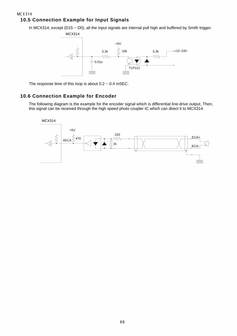
MCX314
66
10.5 Connection Example for Input Signals
In MCX314, except (D15 ~ D0), all the input signals are internal pull high and buffered by Smith trigger.
+5V
0.01µ
3.3k 10k
TLP121
3.3k +12~24V
MCX314
The response time of this loop is about 0.2 ~ 0.4 mSEC.
10.6 Connection Example for Encoder
The following diagram is the example for the encoder signal which is differential line-drive output, Then,this signal can be received through the high speed photo coupler IC which can direct it to MCX314.
MCX314
+5V
470XECA1k
220ECA+
ECA-

MCX314
67
11. Example ProgramThe example C program for MCX314 can complied by Turbo C++ 4.0 and the operation system DOS/V.
#include <stdio.h>#include <conio.h>// -----mcx314 register address definition -----#define adr 0x280 //Basic address#define wr0 0x0 //Command register#define wr1 0x2 //Mode register 1#define wr2 0x4 //Mode register 2#define wr3 0x6 //Mode register 3#define wr4 0x8 //Output register#define wr5 0xa //Interpolation mode register#define wr6 0xc //Low word bits data writing register#define wr7 0xe //High word bits data writing register
#define rr0 0x0 //Main status register#define rr1 0x2 //Status register 1#define rr2 0x4 //Status register 2#define rr3 0x6 //Status register 3#define rr4 0x8 //Input register 1#define rr5 0xa //Input register 2#define rr6 0xc //Low word bits data reading register#define rr7 0xe //High word bits data reading register
#define bp1p 0x4 //BP + direction data register for the first axiscontrol#define bp1m 0x6 //BP − direction data register for the first axiscontrol#define bp2p 0x8 //BP + direction data register for the second axiscontrol#define bp2m 0xa //BP − direction data register for the second axiscontrol#define bp3p 0xc //BP + direction data register for the third axiscontrol#define bp3m 0xe //BP − direction data register for the third axiscontrol
// wreg 1 (axis assignment, data) ----Write register 1 settingvoid wreg1(int axis, int wdata)¡ a
outpw(adr+wr0,(axis<<8)+0xf); //axis assignmentoutpw(adr+wr1, wdata);¡ b
// wreg 2 (axis assignment, data) ----Write register 2 settingvoid wreg2 (int axis, int wdata)¡ a
outpw(adr+wr0,(axis<<8)+0xf); //axis assignmentoutpw(adr+wr2, wdata);¡ b
// wreg 3 (axis assignment, data) -----Write register 3 settingvoid wreg3(int axis, int wdata)¡ a
outpw(adr+wr0, (axis<<8)+0xf); //axis assignmentoutpw(adr+wr3, wdata);¡ b
// command (axis assignment, data) -----For writing commandsvoid command(int axis, int cmd)¡ a
outpw(adr+wr0, (axis<<8)+cmd):¡ b
// range(axis assignment, data) -----For range (R) settingvoid range(int axis, long wdata)¡ a
outpw(adr+wr7,(wdata>>16) & 0xffff);outpw(adr+wr6, wdata & 0xffff);outpw(adr+wr0, (axis<<8) + 0x00);¡ b
// acac(axis assignment, data) -----For S-curve acceleration (K) settingvoid acac(int axis, long wdata)
¡ a
outpw(adr+wr6, wdata);outpw(adr+wr0, (axis<<8) + 0x01);¡ b
// acc(axis assignment, data) -----For acceleration/deceleration (A)settingvoid acc(int axis, long wdata)¡ a
outpw(adr+wr6,wdata);outpw(adr+wr0, (axis<<8) + 0x02);¡ b
// dec( axis assignment, data) -----For deceleration (D) settingvoid dec(int axis, long wdata)¡ a
outpw(adr+wr6, wdata);outpw(adr+wr0, (axis<<8) + 0x03);¡ b
// startv(axis assignment, data) -----For initial speed (SV) settingvoid startv(int axis, long wdata)¡ a
outpw(adr+wr6, wdata):outpw(adr+wr0, (axis<<8) + 0x04);¡ b
// speed(axis assignment, data) -----For drive speed (V) settingvoid speed(int axis, long wdata)¡ a
outpw(adr+wr6, wdata);outpw(adr+wr0, (axis<<8) + 0x05);¡ b
// pulse( axis assignment, data) -For output pulse output/finish point (P)settingvoid pulse(int axis, long wdata)¡ a
outpw(adr+wr7, (wdata>>16) & 0xffff);outpw(adr+wr6, wdata & 0xffff);outpw(adr+wr0, (axis<<8) +0x06);¡ b
// decp(axis assignment, data) -----For manual deceleration (DP) settingvoid decp(int axis, long wdata)¡ a
outpw(adr+wr7, (wdata>>16) & 0xffff);outpw(adr+wr6, wdata & 0xffff);outpw(adr+wr0, (axis<<8) + 0x07);¡ b
// center(axis assignment, data) -----For circular center point (C) settingvoid center(int axis, long wdata)¡ a
outpw(adr+wr7, (wdata>>16) & 0xffff);outpw(adr+wr6, wdata & 0xffff);outpw(adr+wr0, (axis<<8) + 0x08);¡ b
// lp(axis assignment, data) -----For logical position counter (LP ) settingvoid lp(int axis, long wdata)¡ a
outpw(adr+wr7, (wdata>>16) & 0xffff);outpw(adr+wr6, wdata & 0xffff);outpw(adr+wr0, (axis<<8) + 0x09);¡ b
// ep(axis assignment, data) -----For real position counter (EP) settingvoid ep(int axis, long wdata)¡ a
outpw(adr+wr7, (wdata>>16) & 0xffff);outpw(adr+wr6, wdata & 0xffff);outpw(adr+wr0, (axis<<8) + 0x0a);¡ b
// compp(axis assignment, data) -----For COMP+ (CP) setting
MCX314
68
void compp(int axis, long wdata)¡ a
outpw(adr+wr7, (wdata>>16) & 0xffff);outpw(adr+wr6, wdata & 0xffff);outpw(adr+wr0, (axis<<8) + 0x0b);¡ b
// compm(axis assignment, data) -----For COMP− (CM) settingvoid compm(int axis, long wdata)¡ a
outpw(adr+wr7, (wdata>>16) & 0xffff);outpw(adr+wr6, wdata & 0xffff);outpw(adr+wr0, (axis<<8) + 0x0c);¡ b
// accofst(axis assignment, data) ----For acceleration counter shift (AO)settingvoid accofst(int axis, long wdata)¡ a
outpw(adr+wr7, (wdata>>16) & 0xffff);outpw(adr+wr6, wdata & 0xffff);outpw(adr+wr0, (axis<<8) + 0x0d);¡ b
// readlp(axis assignment) -----For logical position counter (LP) readingvoid readlp(int axis)¡ a
long a;long d6;long d7;outpw(adr+wr0, (axis<<8) + 0x10);d6=inpw(adr+rr6);d7=inpw(adr+rr7);a=d6 + (d7<<16);return(a);¡ b
// readep(axis assignment) -----For real position counter (EP) readingvoid readep(int axis)¡ a
long a;long d6;long d7;outpw(adr+wr0, (axis<<8) + 0x11);d6=inpw(adr+rr6);d7=inpw(adr+rr7);a=d6 + (d7<<16);return(a);¡ b
// wait(axis assignment) -----For waiting for drive stopvoid wait(int axis)¡ a
while(inpw(adr+rr0) & axis);¡ b
// next_wait() -----Next data setting of waiting for continuous interpolationvoid next_wait(void)¡ a
while((inpw(adr+rr0) & 0x0200)==0x0);¡ b
// bp_wait() ----- Next data setting of waiting for BP interpolationvoid bp_wait(void)¡ a
while((inpw(adr+rr0) & 0x06000)= =0x6000);¡ b
// homesrch()-----for homeal point searching on whole axisvoid homesrch(void)¡ a // [Action] The same for (1) ~ (3) axes
wreg1(0xf, 0x0008); // If homeal signal (in 1) = OFFspeed(0xf, 2000); // -direction motion will be continuously driven at aspeed of 20000 PPSif((inpw(adr+rr4) & 0x2)= =0x2)
// If IN1 signal = ON, deceleration will be stopped.¡ a
command(0x1, 0x23);¡ b
if((inpw(adr+rr4) & 0x200)= =0x200)¡ a
command(0x2, 0x23);
¡ b
if((inpw(adr+rr5) & 0x2)= =0x2¡ a
command(0x4, 0x23);¡ b
if((inpw(adr+rr5) & 0x200)= =0x200)¡ a
command(0x8, 0x23);¡ b
wait(0xf);wreg1(0xf, 0x000c); //(2) + direction motion will be continuously driven ata speed of 500 PPSspeed(0xf, 50); //When IN1 = OFF, it will be suddenlystoppedcommand(0xf, 0x21);wait(0xf);
wreg1(0xf, 0x0000); //(3) - direction motion will be driven at a speed of40000 PPSspeed(0xf, 40000); //100-pulse shiftpulse(0xf, 100);command(0xf, 0x21);wait(0xf);
lp(0xf, 0); //(4) LP = 0 for X, Y, Z, and U axeswreg2(0xf, 0x0003); //Software limit on X, Y, Z axes: ONcompp(0x1, 100000); //X: -1000 ~ +100000compm(0x1, -1000);compp(0x2, 50000); //Y: -500 ~ +50000compm(ox2, -500);compp(0x4, 10000); //Z: -100 ~ +10000compm(0x4, -100);
//***********<<Main Program>>**************void main(void)¡ a
int count;outpw(adr+wr0, 0x8000); //Software resetfor(count = 0; count<2; ++count);
command(0xf, 0xf); //-----Whole axis mode setting--------outpw(adr+wr1, 0x0000); //Mode register 1 :00000000 00000000outpw(adr+wr2, 0x0000); //Mode register 2 :00000000 00000000outpw(adr+wr3, 0x0000); //Mode register 3 :00000000 00000000outpw(adr+wr4, 0x0000); //General output register00000000 00000000outpw(adr+wr5, 0x0024); //Interpolation mode register00000000 00100100
//-----Initial value settings for whole axis drivingaccofst(0xf,0); //AO = 0range(0xf, 800000) //R = 800000 (Multiple = 10)acac(0xf, 1010); //K = 1010 (Jerk = 619 KPPS/SEC2)acc(0xf, 100); //A = 100 (Acceleration/deceleration=125KPPS/SEC)dec(0xf, 100); //D (Deceleration = 125 KPPS/SEC)startv(0xf, 100); //SV = 100 (Initial Speed = 1000 PPS)speed(0xf, 4000); //V = 40000 (Drive Speed = 40000 PPS)pulse(0xf, 100000); //P = 100000 (output pulse number = 100000)lp(0xf, 0); //LP = 0 (Logical position counter = 0)
homesrch( ); //-----Home searching on whole axis-----
//-----Trapezoidal driving at X and Y axesacc(0x3, 200); (Acceleration/deceleration = 250KPPS/SEC)speed(0x3, 4000); //V = 4000(Drive Speed = 4000 PPS)

MCX314
69
pulse(0x1, 8000); //xP = 8000pulse(0x2, 40000); //yP = 40000command(0x3, 0x20); //- direction constant drivewait(0x3); //Wait for drive stop
wreg3(0x3, 0x0004); //S-curve acceleration/deceleration driving at X andY axesacac(0x3, 1010); //K = 1010 (S-curve Acceleration = 619 KPPS/SEC2)acc(0x3, 200); //A = 200 (Acceleration/Deceleration = 250 KPPS/SEC)speed(0x3, 4000); //V = 4000 (Drive Speed = 4000 PPS)pulse(0x1, 50000); //xP = 50000pulse(0x2, 25000); //yP = 25000command(0x0, 0x21); //- direction constant drivewait(0x3);wreg3(0x3, 0x0000); //S-curve acceleration/deceleration mode clearing
//-----Linear interpolation drive at X and Y axisoutpw(adr+wr5, 0x0124); //ax1 = x, ax2 = y, ax3 = z, linear speed keepsconstantrange(0x1, 800000); //ax1/R = 800000 (Multiple = 10)range(0x2, 1131371); //ax1/R = 800000 x 1.414speed(0x1, 100); //Drive Speed = 1000 PPS constant speedpulse(0x1, 5000); //xP = +5000 (Finish point X = +5000)pulse(0x2, -2000); //yP = -2000 (Finish point Y = -2000)command90x0, 0x30); // 2-axis linear interpolationwait(0x3)
//-----Circular interpolation drive at X and Y axes -----outpw(adr+wr5, 0x0124); //ax1 = x, ax2 = y, ax3 = z, linear speed keepsconstantrange(0x1, 800000); //ax1/R = 800000 (Multiple = 10)range(0x2, 1131371); //ax2/R = 800000 x 1.414speed(0x1, 100); //Drive Speed = 1000 PPS constant speedcenter(0x1, -5000); //xC = 5000 (Center of X = -5000)center(0x2, 0); //yC = 0 (Center of Y = 0)pulse(0x1, 0); //xP = 0 (Finish point of X = 0) Circlepulse(0x2, 0); //yP = 0 (Finish point of Y = 0)command(0x0, 0x33); //CCW circular interpolationwait(0x3);//----- Bit pattern interpolation at X and Y axes-----//(Example of figure2.24)speed(0x1,1); //Drive Speed = 10 PPS constantspeedcommand(0, 0x36); //Bit pattern data writing permission
outpw(adr+bp1p, 0x0000); //0 ~ 15 bits data writingoutpw(adr+bp1m, 0x2bff);outpw(adr+bp2p, 0xffd4);outpw(adr+bp2m, 0x0000);command(0, 0x38); //Stack
outpw(adr+bp1p, 0xf6fe); //16 ~ 31 bits data writingoutpw(adr+bp1m, 0x0000);outpw(adr+bp2p, 0x000f);outpw(adr+bp2m, 0x3fc0);command(0, 0x38);
outpw(adr+bp1p, 0x1fdb); //32 ~ 47 bits data writingoutpw(adr+bp1m, 0x0000);outpw(adr+bp2p, 0x00ff);outpw(adr+bp2m, 0xfc00);command(0, 0x38);
command(0, 0x38); //2-axis BP interpolation drive starting
bp_wait( ); //Wait for data writing
outpw(adr+bp1p, 0x1fdb); //48 ~ 63 bit3 data writingoutpw(adr+bp1m, 0x0000);outpw(adr+bp2p, 0x00ff);outpw(adr+bp2m, 0xfc00);command(0, 0x38);
command(0,0x37); // Bits pattern data writing inhibition
wait(0x3); //Wait for drive stop
//----- Continuous interpolation at X and Y axes (Example of figure2.29)speed(0x1, 100); //Drive Speed = 10 PPS constant speed
pulse(0x1, 4500); // node 1pulse(0x2, 0);command(0, 0x30);
next_wait(); //Wait for next data settingcenter(0x1,0); // node 2center(0x2, 1500);pulse(0x1, 1500);pulse(0x2, 1500);command(0, 0x33);
next_wait();pulse(0x1, 0); // node 3pulse(0x2, 1500);command(0, 0x30);next_wait();center(0x1, -1500); // node 4center(0x2, 0);pulse(0x1, -1500);pulse(0x2, 1500);command(0, 0x33);next_wait(); // node 5pulse(0x1, -4500);pulse(0x2, 0);command(0, 0x30);
next_wait(); // node 6center(0x1, 0);center(0x2, -1500);pulse(0x1, -1500);pulse(0x2, -1500);command(0, 0x33);
next_wait(); //node 7pulse(0x1, 0);pulse(0x2, -1500);command(0, 0x30);
next_wait(); //node 8center(0x1, 1500);center(0x2, 0);pulse(0x1, 1500);pulse(0x2, -1500);command(0, 0x33);
wait(0x3);¡ b

12. Electrical Characteristics
12.1 DC Characteristics
n Absolute Maximum Rated n Recommend Operation Environment
Item Symbol Value Unit Item Symbol Value UnitPower Voltage VDD -0.3 ~ +7.0 V Power Voltage VDD 4.75 ~ 5.25 V
Input voltage VIN -0.3 ~ VDD+0.3 V AmbientTemperature Ta 0 ~ +85 °C
Input Current IIN ± 10 mA
ReservationTemperature TSTG -40 ~ +125 °C
If the user wishes to operate the IC below 0°C,please make contact with our R&D engineer.
n DC Characteristics (Ta = 0 ~ +85°C, VDD = 5V ¡ Ó5%)
Item Mark Condition Min. Typ. Max. Unit Remark
High level input voltage VIH 22 V
Low level input voltage VIL 0.8 V
High level input current IIH VIN=VDD -10 10 µA
VIN=0V -10 10 µA D15~D0 Input signalLow level input current
IILVIN=0V -200 -10 µA Input signal besides D15~D0
IOH=-1µA VDD-0.05 V Note 1
IOH=-4 mA 2.4 V Output Signal besidesD15~D0
High level outputvoltage VOH
IOH=-8 mA 2.4 V D15~D0 Output signal
IOL=1µA 0.05 V
IOL=4 mA 0.4 V Output signal besides D15~D0Low level output voltageVOL
IOL=8 mA 0.4 V D15~D0 output signal
Output leakage current IOZ VOUT=VDD or 0V -10 10 µA D15~D0, BUSYN, INTN
Smith hysteresis voltage VH 0.3 V
Consuming current IDD IIO=0 mA, CLK=16 MHz 52 90 mA
Note1 : BUSYN and INTN output signals have no items for high level output voltage due to the open drainoutput.
n Pin CapacityItem Mark Condition Min. Typ. Max. Unit Remark
Input/ Output capacity CIO 10 pF D15 ~ D0
Input capacity CI
Ta=25°Cf=1 MHz 10 pF Other input pins
12.2 AC Characteristics (Ta = 0 ~ +85°C, VDD = 5V ± 5%, Output load condition: 85 pF + 1 TTL )
12.2.1 Clockn CLK Input Pulse n SCLK Output Signal
tWH tWL
tCYC
CLK
tDFtDR
SCLK
CLK
SCLK will not be output during reset.
Symbol Item Min. Max. Unit
tCYC CLK Cycle 62.5 nS
tWH CLK Hi Level Wavelength 20 nS
tWL CLK Low Level Wavelength 20 nS
tDR CLK↑ → SCLK↑ Delay Time 21 nS
tDF CLK↑→ SCLK↓ Delay Time 23 nS

MCX314
71
12.2.2 Read / Write Cycle
Read cycle Write cycle
Valid Address Valid Address
Data output. Data input.
tCR tRD
tAR
tRA
tRC
tDF tCW
tAW tWW
tDW
tWC
tDH
tWA
The figure shown above is used for 16-bit data bus accessing (H16L8 = Hi). For 8-bit data bus (H16L8 =Low), the address signals shown in the figure become A3~A0, and data signals become D7~D0.
Symbol Item Min. Max. Unit
tAR Address SETUP Time (to RDN ↓) 0 nS
tCR CSN SETUP Time (to RDN ↓) 0 nS
tRD Output Data Delay Time (from RDN ↑) 29 nS
tDF Output Data Reservation Time (from RDN ↑) 0 30 nS
tRC CSN Reservation Time (from RDN ↑) 0 nS
tRA Address Reservation Time (from RDN ↑) 0 nS
tAW Address SETUP Time (to WRN ↓) 0 nS
tCW Established Time for CSN (to WRN ↓) 0 nS
tWW WRN Low Level Wavelength 50 nS
tDW Established Time for Input Data (to WRN ↑) 30 nS
tDH Reservation Time for Input Data (from WRN ↑) 10 nS
tWC CSN Reservation Time (from WRN ↑) 5 nS
tWA Address Reservation Time (from WRN ↑) 5 nS
12.2.3 BUSYN Signal
tDF tWL
It is low when BUSYN is active. And BUSYN is low after 2 SCLK cycles when WRN ↑ active.Mark Item Min. Max. Unit
tDF WRN ↑ → BUSYN ↓ Delay Time 32 nS
tWL BUSYN Low Level Wavelength tCYC x 4+30 nS
tCYC is a cycle of CLK.
12.2.4 SCLK/Output Signal TimingThe following output single is synchronized with SCLK output signal. The level at ACLK ↑ will be changed.Output signals : nPP/PLS, nPM/DIR, nDRIVE, nASND, nDSND, nCMPP, and nCMPM.

MCX314
72
tDI
Output signal
SCLK
Mark Item Min. Max. Unit
tDD SCLK ↑ → Output Signal ↑ ↓ Delay Time 0 20 nS
12.2.5 Input Pulsesn Quadrature Pulses Input Mode (A/B phases)
nECA
nECB
Counting up Counting down
tDE tDE tDE tDE tDE tDE tDE tDE
n Up/Down Pules Input Mode
nPPIN
nPMINtDE tDE
tICYC
tDE tDE
tICYCtIB
l In A/B quadrature pulse input mode, when nECA and nECB input pulses are changed, the value of realposition counter will be changed to the value of those input pulses changed after the period of longestSCLK4 is passed.
l In UP/DOWN pulse input mode, the real position counter will become the value of those input pulseschanged, after the period between the beginning of nPPIN, nPMIN ↑ and the time of SCLK 4 cycle ispassed.Mark Item Min. Max. Unit
tDE nECA and nECB Phase Difference Time tCYC x 2+20 nS
tIH nPPIN and nPMIN Hi Level Wavelength 30 nS
tIL nPPIN and nPMIN Low Level Wavelength 30 nS
tiCYC nPPIN and nPMIN Cycle tCYC x 2+20 nS
tIB nPPIN ↑ ←→ nPMIN ↑ Time tCYC x 2+20 nS
12.2.6 General Purpose Input / Output SignalsThe figure shown at the lower left hand side illustrates the delay time when input signals nIN3 ~ 0, nEXPP,nEXPM, nINPOS, and nALARM are read through RR4 and RR5 registers.The figure shown at the lower right hand side illustrates the delay time when writing general output signaldata into nWR3 and nWR4.
tDI
Input signal
RDN
D15~0
tDO
WRN
nOUT7~0
D15~0
Mark Item Min. Max. Unit
tDI Input Signal → Data Delay Time 32 nS
tDO WRN ↑ → nOUT7~0 Established Time 32 nS
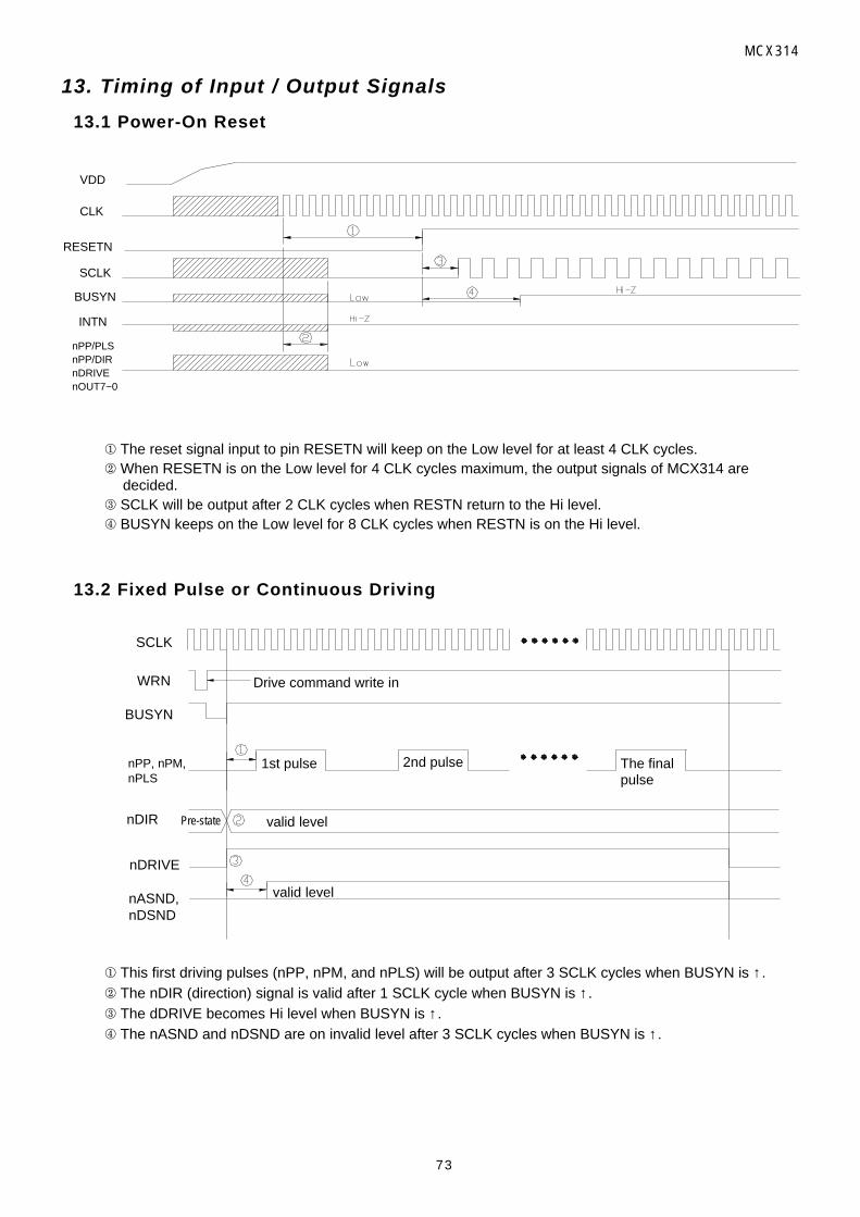
MCX314
73
13. Timing of Input / Output Signals
13.1 Power-On Reset
VDD
CLK
RESETN
SCLK
BUSYN
INTN
nPP/PLSnPP/DIRnDRIVEnOUT7~0
¬ The reset signal input to pin RESETN will keep on the Low level for at least 4 CLK cycles. When RESETN is on the Low level for 4 CLK cycles maximum, the output signals of MCX314 are
decided.® SCLK will be output after 2 CLK cycles when RESTN return to the Hi level.¯ BUSYN keeps on the Low level for 8 CLK cycles when RESTN is on the Hi level.
13.2 Fixed Pulse or Continuous Driving
valid level
valid level
Drive command write in
1st pulse 2nd pulse The finalpulse
Pre-state
SCLK
WRN
BUSYN
nPP, nPM,nPLS
nDIR
nDRIVE
nASND,nDSND
¬ This first driving pulses (nPP, nPM, and nPLS) will be output after 3 SCLK cycles when BUSYN is ↑. The nDIR (direction) signal is valid after 1 SCLK cycle when BUSYN is ↑.® The dDRIVE becomes Hi level when BUSYN is ↑.¯ The nASND and nDSND are on invalid level after 3 SCLK cycles when BUSYN is ↑.

MCX314
74
13.3 Interpolation
valid level
1st pulse 2nd pulse
SCLK
WRN
BUSYN
nPP, nPM,nPLS
nDIR
nDRIVE
valid levelinvalid invalid invalid
¬ The first pulses (nPP, nPM, and nPLS) of interpolation driving will be output after 4 SCLK cycles whenBUSYN is ↑.
nDRIVE will become Hi level after 1 SCLK cycle when BUSYN is ↑.® DIR signal keeps the active level in 1 SCLK cycle before and after the Hi level pulse outputting.
13.4 Start Driving after Hold Command
1st pulse 2nd pulse
SCLK
WRN
BUSYN
nPP, nPM,nPLS
nDRIVE
¬ The pulses (nPP, nPM, and nPLS) of each axis will start outputting after 3 SCLK cycles when BUSYN is↑.
nDRIVE will become Hi level when BUSYN is ↑ for each axis.
13.5 Sudden Stop
The following figure illustrates the timing of sudden stop. The sudden stop input signals are EMGN,nLMTP/M (When the sudden stop mode is engaged), and nALARM.When sudden stop input signal becomes active, or the sudden stop command is written, it will stop theoutput of pulses immediately.The width of external signals input for sudden stop must be more than 1 SCLK cycle. The stop function willnot be active if the width is less 1 SCLK cycle.
nDSND
nPP, nPM, nPLS
activeDecelerating signalDecelerating command write in
SCLK
13.6 Decelerating Stop
The following figure illustrates the timing of decelerating stop input signal and decelerating commands. Thedecelerating stop signal are nIN3 ~ 0 and nLMTP/M (When the decelerating mode is engaged)

MCX314
75
When speed decelerating signals become active, or the decelerating stop command is written, thedecelerating stop function will be performed.
nDSND
nPP, nPM, nPLS
activeDecelerating signalDecelerating command write in

MCX314
76
14. Pinout
Unit : mm

MCX314
77
15. Specificationsn Control Axis 4 axesn Data Bus 16/8 bits selectable
Interpolation Functionsn 2-axes / 3-axes Linear Interpolation
Interpolation Range Each axis -8,388,608 ~ +8,388,607Interpolation Speed 1 ~ 4 MPPSInterpolation Accuracy ± 0.5 LSB (Within the range of whole interpolation)
n Circular InterpolationInterpolation Range Each axis -8,388,608 ~ +8,388,607Interpolation Speed 1 ~ 4 MPPSInterpolation Accuracy ± 1 LSB (Within the range of whole interpolation)
n 2 axes / 3 axes Bit Pattern InterpolationInterpolation Speed 1 ~ 4 MPPS (Dependent on CPU data writing time)
n Related Functions of InterpolationlCan select any axis lConstant vector speed lContinuous interpolationlSingle step interpolation (Command/external signals)
Common Specifications of Each Axisn Drive Pulses Output (When CLK = 16 MHz)
Pulse Output Speed Range 1PPS ~ 4MPPSPulse Output Accuracy within ± 0.1% (according to the setting speed)S-curve Jerk 954 ~ 31.25¡ Ñ109PPS/S2
Accelerating / Decelerating Speed 125 ~ 500¡ Ñ106PPS/S
Drive Speed 1 ~ 4¡ Ñ106 PPSOutput-pulse Number 0 ~ 268435455 / unlimitedSpeed Curve quadrature / trapezoidal / parabolic S-curveIndex Drive Deceleration Mode auto / manualOutput-pulse numbers and drive speeds changeable during the drivingIndependent 2-pulse system or 1-pulse 1-direction system selectableLogical levels of pulse selectable
n Encoder InputA/B quadrature pulse style or Up/Down pulse style selectablePulse of 1, 2 and 4 divisions selectable (A/B quadrature pulse style)
n Position CounterLogic Position Counter (for output pulse t) range -2,147,483,648 ~ +2,147,483,647Real Position Counter (for feedback pulse) range -2,147,483,648 ~ +2,147,483,647Data read and write possible
MCX314
78
n Comparison RegisterCOMP + Register Position comparison range -2,147,483,648 ~ +2,147,483,647COMP − Register Position comparison range -2,147,483,648 ~ +2,147,483,647Status and signal outputs for the comparisons of position countersSoftware limit functioned
n Interrupt (Interpolations Excluded)The factors of occurring interrupt:..the drive-pulse outputting..the start / finish of a constant-speed drive during the acceleration / deceleration driving..the end of the driving..the volume of position counter¡ Ùthe volume of COMP-
..the volume of position counter¡ Õthe volume of COMP-
..the volume of position counter¡ Ùthe volume of COMP+
..the volume of position counter¡ Õthe volume of COMP+Enable / disable for these factors selectable
n External Signal for DrivingEXPP and EXPM signals for fixed pulse / continuous drive
n External Deceleration / Sudden Stop SignalIN0 ~ 3 4 points for each axisEnable / disable and logical levels selectable
n Servo Motor Input SignalALARM (Alarm)INPOS (In Position Check)Enable / disable and logical levels selectable
n General Output SignalOUT0 ~ 7 8 points for each axis (wherein 4 points use with drive status output signal pin)
n Driving Status Signal OutputASND (speed accelerating), DSND (speed decelerating),CMPP (position¡ ÙCOMP+), CMPM (position¡ ÕCOMP-)Drive status and status registers readable
n Limit Signals Input2 points, for each + and - sideLogical levels and decelerating / sudden stop selectable
n Emergency Stop Signal InputEMG, 1 point for 4 axes
n Electrical Characters
Temperature Range for Driving 0 ~ +45°C (32ºF ~185ºF)Power Voltage for Driving ± 5V ± 5 % (max. power consumption: 90mA)Input / Output Signal Level CMOS, TTL connectableInput Clock Pulse 16,000 MHz (Standard)
n Package 144-pin plastic QFP, pitch = 0.65mmDimension : 30.9 x 30.9 x 4.36 mm

MCX314
1
Appendix A: Speed Curve Profile
The following curves are based on the test records from MCX314 output drive pulses and speed curve traces.
The complete S-curve acceleration / deceleration is the curve drive, without linear acceleration / deceleration,before the appointed drive speed is reached. Partial S-curve acceleration / deceleration is with a period oflinear acceleration / deceleration before the appointed drive speed is reached.
n 40KPPS Full S-curve Acceleration / DecelerationR=800000 (Rate:10), K=700, A=D=200, SV=100, V=4000, A0=50 Auto Decelerating Mode
Jerk=893KPPS/ SEC2
Accel. / Decel. =250KPPS/SECInitial Speed=1000PPSDrive Speed=40KPPS
Output Pulse P=50000
n 40KPPS Partial S-curve Acceleration / DecelerationR=800000 (Rate:10), K=300, A=D=150, SV=100, V=4000, A0=20 Auto Decelerating Mode
Jerk=2083KPPS/ SEC2
Accel. / Decel. =188KPPS/SECInitial Speed=1000PPSDrive Speed=40KPPS
Output Pulse P=50000

MCX314
2
n 8000PPS complete S-curve Acceleration / Deceleration R=8000000 (Rate:1), K=2000, A=D=500, SV=100, V=8000, A0=0 Auto Decelerating Mode
Jerk=31KPPS/ SEC2
Accel. / Decel. =62.5KPPS/SECInitial Speed=100PPSDrive Speed=8000PPS
Output Pulse P=20000
n 8000PPS Partial S-curve Acceleration / Deceleration R=800000 (Rate: 1), K=1000, A=D=100, SV=100, V=8000, A0=0 Auto Decelerating Mode
Jerk=62.5KPPS/ SEC2
Accel. / Decel. =12.5KPPS/SECInitial Speed=100PPSDrive Speed=8000PPS
Output Pulse P=20000
n 400KPPS Full S-curve Acceleration / Deceleration R=80000(Rate:100),K=2000,A=D=100,SV=10,V=4000, A0=1000 Auto Decelerating Mode
Jerk=3.13MPPS/SEC2
Accel. / Decel. =1.25MPPS/SEC Initial Speed=1000PPS
Drive Speed=400KPPS
Output Pulse P=400000
n 400KPPS Partial S-curve Acceleration / Deceleration R=80000 (Rate: 100), K=500, A=D=100, SV=10, V=4000, A0=0 Auto Decelerating Mode
Jerk=12.5MPPS/ SEC2
Accel. / Decel. =1.25MPPS/SECInitial Speed=1000PPSDrive Speed=400KPPS
Output Pulse P=400000

MCX314
3
n Speed Alterations in a Continuous S-curve Acceleration / Deceleration Drive R=800000 (Rate: 10), K=2000, A=D=100, SV=100, V=1000¡ ÷2000¡ ÷4000¡ ÷decelerating stop
Jerk=312.5KPPS/ SEC2
Jerk(decel.)=125KPPS/SECInitial Speed=1000PPSDrive Speed=10K¡ ÷20K¡ ÷40KPPS
n 40KPPS Linear Acceleration / Deceleration
R=800000 (Rate: 10), A=D=100, SV=100, V=4000 WR3/D2, D1, D0=0, 0, 0 Trapezoidal Mode, Auto Decelerating Mode
Accel./ Decel. =125KPPS/ SECInitial Speed=100PPSDrive Speed=40000PPS
Output Pulse P=40000
n Triangle wave Avoiding during the Linear Acceleration / Deceleration
When K=1 (Jerk: Maxium) in the S-curve Accel./ Decel. Mode, “1/4output pulses” principle can be engaged. Even the output pulses arefew, the drive is a trapezoidal drive. R=800000 (Rate: 10), K=1, A=D=100, SV=100, V=4000 WR3/D2, D1, D0=1, 0, 0 S-curve Mode, Auto Decelerating Mode
Jerk =625MPPS/ SEC2
Accel./ Decel. =125KPPS/SECInitial Speed=1000PPSDrive Speed=40000PPS
Output Pulse P=40000
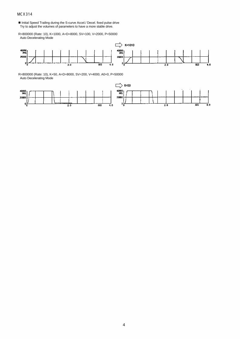
MCX314
4
n Initial Speed Trailing during the S-curve Accel./ Decel. fixed pulse drive Try to adjust the volumes of parameters to have a more stable drive.
R=800000 (Rate: 10), K=1000, A=D=8000, SV=100, V=2000, P=50000 Auto Decelerating Mode
R=800000 (Rate: 10), K+50, A=D=8000, SV=200, V=4000, A0=0, P=50000 Auto Decelerating Mode