Embed Size (px)
Citation preview
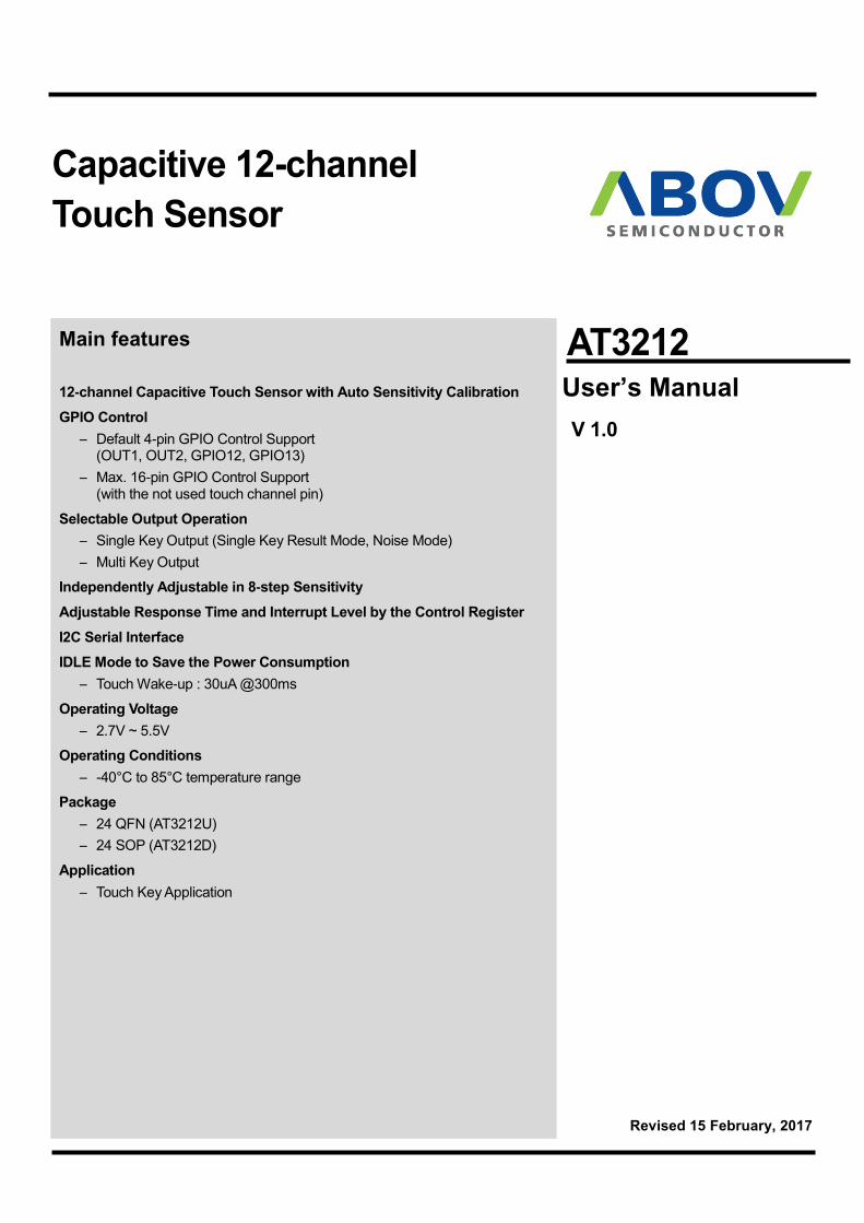
Main features
12-channel Capacitive Touch Sensor with Auto Sensitivity Calibration
GPIO Control
– Default 4-pin GPIO Control Support (OUT1, OUT2, GPIO12, GPIO13)
– Max. 16-pin GPIO Control Support (with the not used touch channel pin)
Selectable Output Operation
– Single Key Output (Single Key Result Mode, Noise Mode)
– Multi Key Output
Independently Adjustable in 8-step Sensitivity
Adjustable Response Time and Interrupt Level by the Control Register
I2C Serial Interface
IDLE Mode to Save the Power Consumption
– Touch Wake-up : 30uA @300ms
Operating Voltage
– 2.7V ~ 5.5V
Operating Conditions
– -40°C to 85°C temperature range
Package
– 24 QFN (AT3212U)
– 24 SOP (AT3212D)
Application
– Touch Key Application
V 1.0
Revised 15 February, 2017
User’s Manual
2 AT3212
AT3212 ABOV Semiconductor Co., Ltd.
Revision history
Version Date Revision list
1.0 2017.02.15 First Release
Version 1.0
Published by FAE team
2017 ABOV Semiconductor Co. Ltd. all rights reserved.
Additional information of this manual may be served by ABOV Semiconductor offices in Korea or distributors.
ABOV Semiconductor reserves the right to make changes to any information here in at any time without notice.
The information, diagrams and other data in this manual are correct and reliable;
However, ABOV Semiconductor is in no way responsible for any violations of patents or other rights of the third
party generated by the use of this manual.
3 AT3212
AT3212 ABOV Semiconductor Co., Ltd.
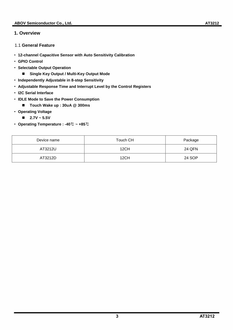
1. Overview
General Feature 1.1
• 12-channel Capacitive Sensor with Auto Sensitivity Calibration
• GPIO Control
• Selectable Output Operation
Single Key Output / Multi-Key Output Mode
• Independently Adjustable in 8-step Sensitivity
• Adjustable Response Time and Interrupt Level by the Control Registers
• I2C Serial Interface
• IDLE Mode to Save the Power Consumption
Touch Wake up : 30uA @ 300ms
• Operating Voltage
2.7V ~ 5.5V
• Operating Temperature : -40℃ ~ +85℃
Device name Touch CH Package
AT3212U 12CH 24 QFN
AT3212D 12CH 24 SOP
4 AT3212
AT3212 ABOV Semiconductor Co., Ltd.
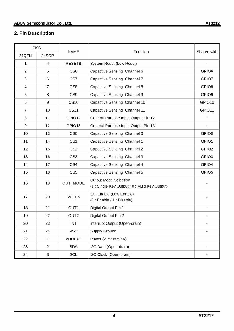
2. Pin Description
PKG NAME Function Shared with
24QFN 24SOP
1 4 RESETB System Reset (Low Reset) -
2 5 CS6 Capactive Sensing Channel 6 GPIO6
3 6 CS7 Capactive Sensing Channel 7 GPIO7
4 7 CS8 Capactive Sensing Channel 8 GPIO8
5 8 CS9 Capactive Sensing Channel 9 GPIO9
6 9 CS10 Capactive Sensing Channel 10 GPIO10
7 10 CS11 Capactive Sensing Channel 11 GPIO11
8 11 GPIO12 General Purpose Input Output Pin 12 -
9 12 GPIO13 General Purpose Input Output Pin 13 -
10 13 CS0 Capactive Sensing Channel 0 GPIO0
11 14 CS1 Capactive Sensing Channel 1 GPIO1
12 15 CS2 Capactive Sensing Channel 2 GPIO2
13 16 CS3 Capactive Sensing Channel 3 GPIO3
14 17 CS4 Capactive Sensing Channel 4 GPIO4
15 18 CS5 Capactive Sensing Channel 5 GPIO5
16 19 OUT_MODE Output Mode Selection
(1 : Single Key Output / 0 : Multi Key Output) -
17 20 I2C_EN I2C Enable (Low Enable)
(0 : Enable / 1 : Disable) -
18 21 OUT1 Digital Output Pin 1 -
19 22 OUT2 Digital Output Pin 2 -
20 23 INT Interrupt Output (Open-drain) -
21 24 VSS Supply Ground -
22 1 VDDEXT Power (2.7V to 5.5V)
23 2 SDA I2C Data (Open-drain) -
24 3 SCL I2C Clock (Open-drain) -
5 AT3212
AT3212 ABOV Semiconductor Co., Ltd.
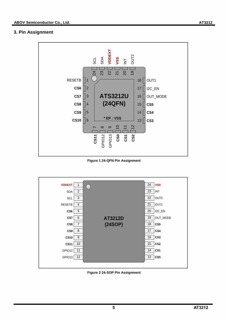
3. Pin Assignment
ATS3212U
(24QFN)
SC
LC
S1
1
SD
A
VD
DE
XT
VS
S
INT
OU
T2
GP
IO1
2
GP
IO1
3
CS
0
CS
1
CS
2
I2C_EN
OUT1
CS5
OUT_MODE
CS3
CS4
CS6
RESETB
CS8
CS7
CS10
CS9
* EP : VSS
1
4
3
2
5
6
18
15
16
17
14
13
24
21
22
23
20
19
7 1098 11
12
Figure 1 24-QFN Pin Assignment
AT3212D
(24SOP)
1
4
3
2
VDDEXT
5
8
7
6
VSS
9
12
11
10
24
21
22
23
20
17
18
19
16
13
14
15
SDA
RESETB
SCL
CS6
CS7
CS8
CS9
CS10
CS11
GPIO12
GPIO13
INT
OUT2
OUT1
I2C_EN
OUT_MODE
CS5
CS4
CS3
CS2
CS1
CS0
Figure 2 24-SOP Pin Assignment
6 AT3212
AT3212 ABOV Semiconductor Co., Ltd.
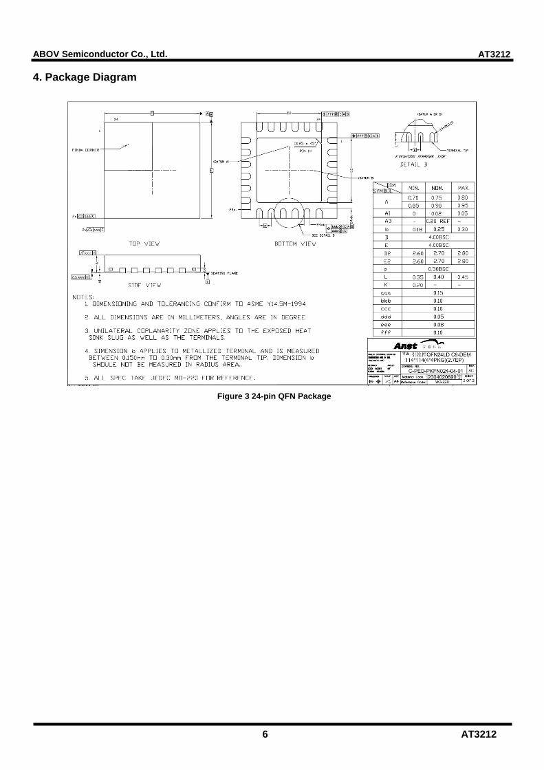
4. Package Diagram
Figure 3 24-pin QFN Package
7 AT3212
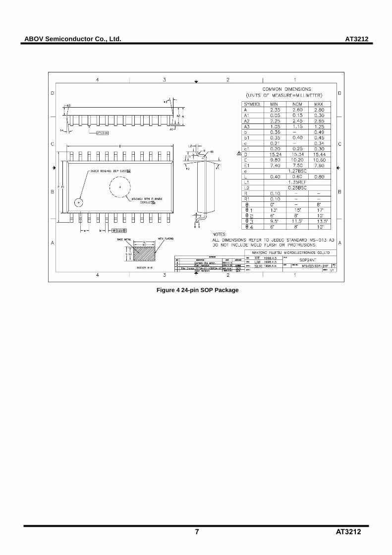
AT3212 ABOV Semiconductor Co., Ltd.
Figure 4 24-pin SOP Package
8 AT3212
AT3212 ABOV Semiconductor Co., Ltd.
5. Electrical Characteristics
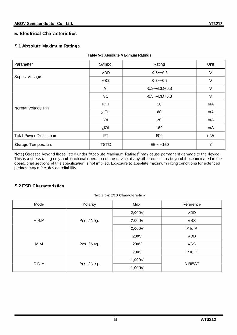
Absolute Maximum Ratings 5.1
Table 5-1 Absolute Maximum Ratings
Parameter Symbol Rating Unit
Supply Voltage VDD -0.3~+6.5 V
VSS -0.3~+0.3 V
Normal Voltage Pin
VI -0.3~VDD+0.3 V
VO -0.3~VDD+0.3 V
IOH 10 mA
∑IOH 80 mA
IOL 20 mA
∑IOL 160 mA
Total Power Dissipation PT 600 mW
Storage Temperature TSTG -65 ~ +150 ℃
Note) Stresses beyond those listed under “Absolute Maximum Ratings” may cause permanent damage to the device. This is a stress rating only and functional operation of the device at any other conditions beyond those indicated in the operational sections of this specification is not implied. Exposure to absolute maximum rating conditions for extended periods may affect device reliability.
ESD Characteristics 5.2
Table 5-2 ESD Characteristics
Mode Polarity Max. Reference
H.B.M Pos. / Neg.
2,000V VDD
2,000V VSS
2,000V P to P
M.M Pos. / Neg.
200V VDD
200V VSS
200V P to P
C.D.M Pos. / Neg. 1,000V
DIRECT 1,000V
9 AT3212
AT3212 ABOV Semiconductor Co., Ltd.
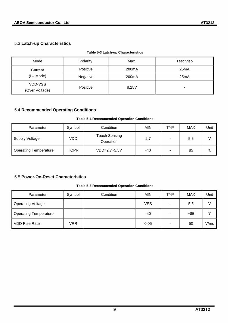
Latch-up Characteristics 5.3
Table 5-3 Latch-up Characteristics
Mode Polarity Max. Test Step
Current
(I – Mode)
Positive 200mA 25mA
Negative 200mA 25mA
VDD-VSS
(Over Voltage) Positive 8.25V -
Recommended Operating Conditions 5.4
Table 5-4 Recommended Operation Conditions
Parameter Symbol Condition MIN TYP MAX Unit
Supply Voltage VDD Touch Sensing
Operation 2.7 - 5.5 V
Operating Temperature TOPR VDD=2.7~5.5V -40 - 85 ℃
Power-On-Reset Characteristics 5.5
Table 5-5 Recommended Operation Conditions
Parameter Symbol Condition MIN TYP MAX Unit
Operating Voltage VSS - 5.5 V
Operating Temperature -40 - +85 ℃
VDD Rise Rate VRR 0.05 - 50 V/ms
10 AT3212
AT3212 ABOV Semiconductor Co., Ltd.
6. I2C Interface
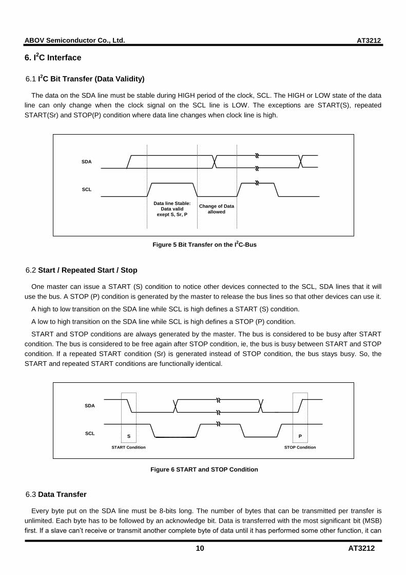
I2C Bit Transfer (Data Validity) 6.1
The data on the SDA line must be stable during HIGH period of the clock, SCL. The HIGH or LOW state of the data
line can only change when the clock signal on the SCL line is LOW. The exceptions are START(S), repeated
START(Sr) and STOP(P) condition where data line changes when clock line is high.
Start / Repeated Start / Stop 6.2
One master can issue a START (S) condition to notice other devices connected to the SCL, SDA lines that it will
use the bus. A STOP (P) condition is generated by the master to release the bus lines so that other devices can use it.
A high to low transition on the SDA line while SCL is high defines a START (S) condition.
A low to high transition on the SDA line while SCL is high defines a STOP (P) condition.
START and STOP conditions are always generated by the master. The bus is considered to be busy after START
condition. The bus is considered to be free again after STOP condition, ie, the bus is busy between START and STOP
condition. If a repeated START condition (Sr) is generated instead of STOP condition, the bus stays busy. So, the
START and repeated START conditions are functionally identical.
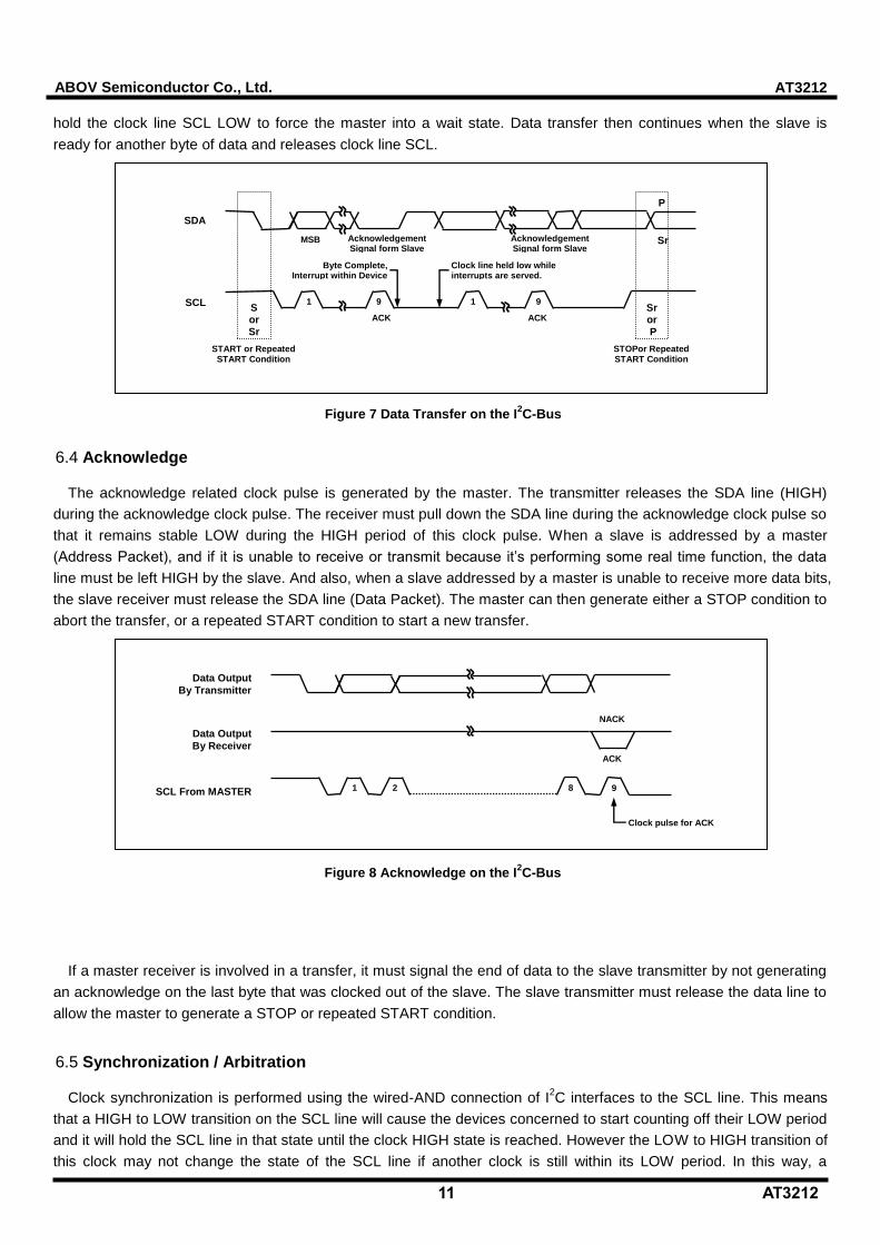
Data Transfer 6.3
Every byte put on the SDA line must be 8-bits long. The number of bytes that can be transmitted per transfer is
unlimited. Each byte has to be followed by an acknowledge bit. Data is transferred with the most significant bit (MSB)
first. If a slave can’t receive or transmit another complete byte of data until it has performed some other function, it can
SCL
SDA
Data line Stable: Data valid
exept S, Sr, P
Change of Data
allowed
SCL
SDA
START Condition
S P
STOP Condition
Figure 5 Bit Transfer on the I2C-Bus
Figure 6 START and STOP Condition
11 AT3212
AT3212 ABOV Semiconductor Co., Ltd.
hold the clock line SCL LOW to force the master into a wait state. Data transfer then continues when the slave is
ready for another byte of data and releases clock line SCL.
Acknowledge 6.4
The acknowledge related clock pulse is generated by the master. The transmitter releases the SDA line (HIGH)
during the acknowledge clock pulse. The receiver must pull down the SDA line during the acknowledge clock pulse so
that it remains stable LOW during the HIGH period of this clock pulse. When a slave is addressed by a master
(Address Packet), and if it is unable to receive or transmit because it’s performing some real time function, the data
line must be left HIGH by the slave. And also, when a slave addressed by a master is unable to receive more data bits,
the slave receiver must release the SDA line (Data Packet). The master can then generate either a STOP condition to
abort the transfer, or a repeated START condition to start a new transfer.
If a master receiver is involved in a transfer, it must signal the end of data to the slave transmitter by not generating
an acknowledge on the last byte that was clocked out of the slave. The slave transmitter must release the data line to
allow the master to generate a STOP or repeated START condition.
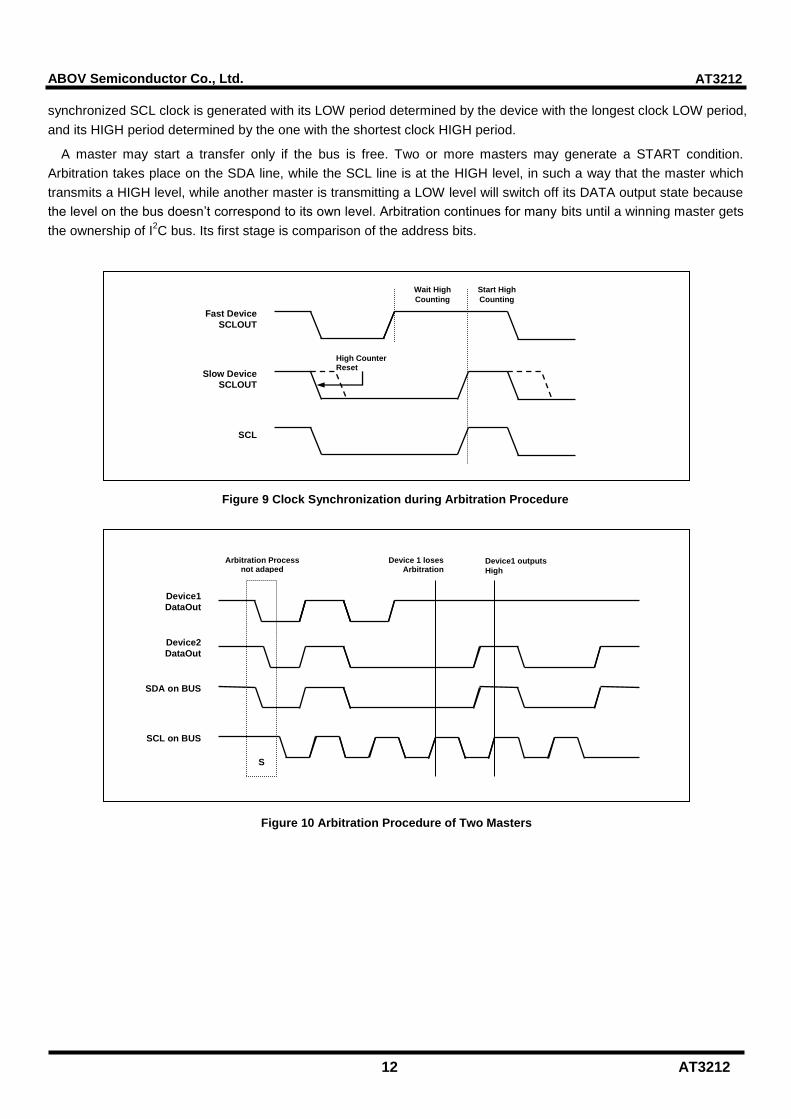
Synchronization / Arbitration 6.5
Clock synchronization is performed using the wired-AND connection of I2C interfaces to the SCL line. This means
that a HIGH to LOW transition on the SCL line will cause the devices concerned to start counting off their LOW period
and it will hold the SCL line in that state until the clock HIGH state is reached. However the LOW to HIGH transition of
this clock may not change the state of the SCL line if another clock is still within its LOW period. In this way, a
1 2 8
Data Output
By Transmitter
9
ACK
NACK
Clock pulse for ACK
Data Output
By Receiver
SCL From MASTER
START or Repeated START Condition
S or Sr
STOPor Repeated START Condition
Sr or P
MSB Acknowledgement Signal form Slave
Acknowledgement Signal form Slave
Byte Complete, Interrupt within Device
Clock line held low while interrupts are served.
1 9 1 9
ACK ACK
SDA
SCL
Sr
P
Figure 7 Data Transfer on the I2C-Bus
Figure 8 Acknowledge on the I2C-Bus
12 AT3212
AT3212 ABOV Semiconductor Co., Ltd.
synchronized SCL clock is generated with its LOW period determined by the device with the longest clock LOW period,
and its HIGH period determined by the one with the shortest clock HIGH period.
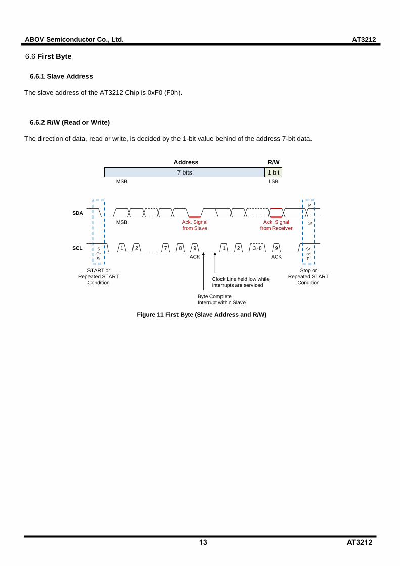
A master may start a transfer only if the bus is free. Two or more masters may generate a START condition.
Arbitration takes place on the SDA line, while the SCL line is at the HIGH level, in such a way that the master which
transmits a HIGH level, while another master is transmitting a LOW level will switch off its DATA output state because
the level on the bus doesn’t correspond to its own level. Arbitration continues for many bits until a winning master gets
the ownership of I2C bus. Its first stage is comparison of the address bits.
High Counter Reset
Fast Device
SCLOUT
Slow Device SCLOUT
SCL
Wait High
Counting
Start High
Counting
Device1
DataOut
SCL on BUS
Device2
DataOut
SDA on BUS
S
Arbitration Process not adaped
Device 1 loses Arbitration
Device1 outputs
High
Figure 9 Clock Synchronization during Arbitration Procedure
Figure 10 Arbitration Procedure of Two Masters
13 AT3212
AT3212 ABOV Semiconductor Co., Ltd.
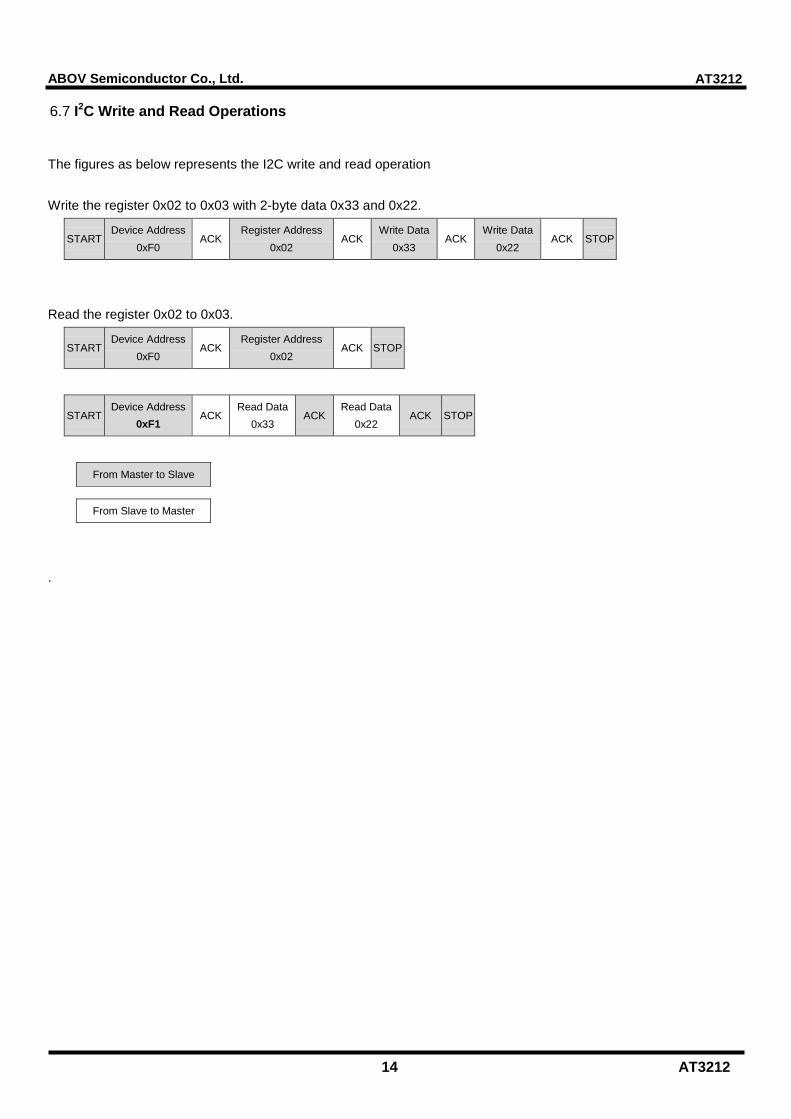
First Byte 6.6
6.6.1 Slave Address
The slave address of the AT3212 Chip is 0xF0 (F0h).
6.6.2 R/W (Read or Write)
The direction of data, read or write, is decided by the 1-bit value behind of the address 7-bit data.
MSB
1 2 7 8 9
ACK ACK
1 2 3~8 9SCL
SDA
START or
Repeated START
Condition
Stop or
Repeated START
Condition
Ack. Signal
from Slave
Ack. Signal
from Receiver
S
Or
Sr
Sr
or
P
P
Sr
Byte Complete
Interrupt within Slave
Clock Line held low while
interrupts are serviced
7 bits 1 bit
Address R/W
MSB LSB
Figure 11 First Byte (Slave Address and R/W)
14 AT3212
AT3212 ABOV Semiconductor Co., Ltd.
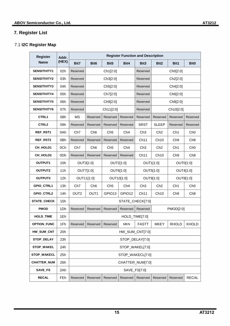
I2C Write and Read Operations 6.7
The figures as below represents the I2C write and read operation
Write the register 0x02 to 0x03 with 2-byte data 0x33 and 0x22.
START Device Address
0xF0 ACK
Register Address
0x02 ACK
Write Data
0x33 ACK
Write Data
0x22 ACK STOP
Read the register 0x02 to 0x03.
START Device Address
0xF0 ACK
Register Address
0x02 ACK STOP
START Device Address
0xF1 ACK
Read Data
0x33 ACK
Read Data
0x22 ACK STOP
From Master to Slave
From Slave to Master
.
15 AT3212
AT3212 ABOV Semiconductor Co., Ltd.
7. Register List
I2C Register Map 7.1
Register
Name
Addr. (HEX)
Register Function and Description
Bit7 Bit6 Bit5 Bit4 Bit3 Bit2 Bit1 Bit0
SENSITIVITY1 02h Reserved Ch1[2:0] Reserved Ch0[2:0]
SENSITIVITY2 03h Reserved Ch3[2:0] Reserved Ch2[2:0]
SENSITIVITY3 04h Reserved Ch5[2:0] Reserved Ch4[2:0]
SENSITIVITY4 05h Reserved Ch7[2:0] Reserved Ch6[2:0]
SENSITIVITY5 06h Reserved Ch9[2:0] Reserved Ch8[2:0]
SENSITIVITY6 07h Reserved Ch11[2:0] Reserved Ch10[2:0]
CTRL1 08h MS Reserved Reserved Reserved Reserved Reserved Reserved Reserved
CTRL2 09h Reserved Reserved Reserved Reserved SRST SLEEP Reserved Reserved
REF_RST1 0Ah Ch7 Ch6 Ch5 Ch4 Ch3 Ch2 Ch1 Ch0
REF_RST2 0Bh Reserved Reserved Reserved Reserved Ch11 Ch10 Ch9 Ch8
CH_HOLD1 0Ch Ch7 Ch6 Ch5 Ch4 Ch3 Ch2 Ch1 Ch0
CH_HOLD2 0Dh Reserved Reserved Reserved Reserved Ch11 Ch10 Ch9 Ch8
OUTPUT1 10h OUT3[1:0] OUT2[1:0] OUT1[1:0] OUT0[1:0]
OUTPUT2 11h OUT7[1:0] OUT6[1:0] OUT5[1:0] OUT4[1:0]
OUTPUT3 12h OUT11[1:0] OUT10[1:0] OUT9[1:0] OUT8[1:0]
GPIO_CTRL1 13h Ch7 Ch6 Ch5 Ch4 Ch3 Ch2 Ch1 Ch0
GPIO_CTRL2 14h OUT2 OUT1 GPIO13 GPIO12 Ch11 Ch10 Ch9 Ch8
STATE_CHECK 15h STATE_CHECK[7:0]
PMOD 1Dh Reserved Reserved Reserved Reserved Reserved PMOD[2:0]
HOLD_TIME 1Eh HOLD_TIME[7:0]
OPTION_FUNC 1Fh Reserved Reserved Reserved MKN FASTT MKEY RHOLD KHOLD
HW_SUM_CNT 20h HW_SUM_CNT[7:0]
STOP_DELAY 23h STOP_DELAY[7:0]
STOP_WAKEL 24h STOP_WAKEL[7:0]
STOP_WAKECL 25h STOP_WAKECL[7:0]
CHATTER_NUM 26h CHATTER_NUM[7:0]
SAVE_FS 2Ah SAVE_FS[7:0]
RECAL FEh Reserved Reserved Reserved Reserved Reserved Reserved Reserved RECAL
16 AT3212
AT3212 ABOV Semiconductor Co., Ltd.
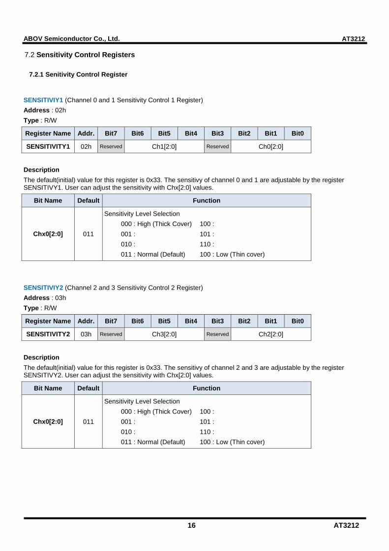
Sensitivity Control Registers 7.2
7.2.1 Senitivity Control Register
SENSITIVIY1 (Channel 0 and 1 Sensitivity Control 1 Register)
Address : 02h
Type : R/W
Register Name Addr. Bit7 Bit6 Bit5 Bit4 Bit3 Bit2 Bit1 Bit0
SENSITIVITY1 02h Reserved Ch1[2:0] Reserved Ch0[2:0]
Description
The default(initial) value for this register is 0x33. The sensitivy of channel 0 and 1 are adjustable by the register SENSITIVY1. User can adjust the sensitivity with Chx[2:0] values.
Bit Name Default Function
Chx0[2:0] 011
Sensitivity Level Selection
000 : High (Thick Cover) 100 :
001 : 101 :
010 : 110 :
011 : Normal (Default) 100 : Low (Thin cover)
SENSITIVIY2 (Channel 2 and 3 Sensitivity Control 2 Register)
Address : 03h
Type : R/W
Register Name Addr. Bit7 Bit6 Bit5 Bit4 Bit3 Bit2 Bit1 Bit0
SENSITIVITY2 03h Reserved Ch3[2:0] Reserved Ch2[2:0]
Description
The default(initial) value for this register is 0x33. The sensitivy of channel 2 and 3 are adjustable by the register SENSITIVY2. User can adjust the sensitivity with Chx[2:0] values.
Bit Name Default Function
Chx0[2:0] 011
Sensitivity Level Selection
000 : High (Thick Cover) 100 :
001 : 101 :
010 : 110 :
011 : Normal (Default) 100 : Low (Thin cover)
17 AT3212
AT3212 ABOV Semiconductor Co., Ltd.
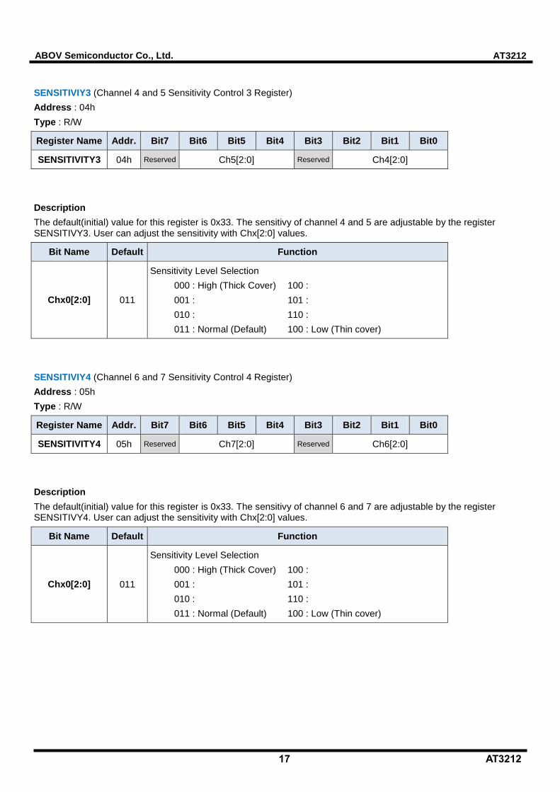
SENSITIVIY3 (Channel 4 and 5 Sensitivity Control 3 Register)
Address : 04h
Type : R/W
Register Name Addr. Bit7 Bit6 Bit5 Bit4 Bit3 Bit2 Bit1 Bit0
SENSITIVITY3 04h Reserved Ch5[2:0] Reserved Ch4[2:0]
Description
The default(initial) value for this register is 0x33. The sensitivy of channel 4 and 5 are adjustable by the register SENSITIVY3. User can adjust the sensitivity with Chx[2:0] values.
Bit Name Default Function
Chx0[2:0] 011
Sensitivity Level Selection
000 : High (Thick Cover) 100 :
001 : 101 :
010 : 110 :
011 : Normal (Default) 100 : Low (Thin cover)
SENSITIVIY4 (Channel 6 and 7 Sensitivity Control 4 Register)
Address : 05h
Type : R/W
Register Name Addr. Bit7 Bit6 Bit5 Bit4 Bit3 Bit2 Bit1 Bit0
SENSITIVITY4 05h Reserved Ch7[2:0] Reserved Ch6[2:0]
Description
The default(initial) value for this register is 0x33. The sensitivy of channel 6 and 7 are adjustable by the register SENSITIVY4. User can adjust the sensitivity with Chx[2:0] values.
Bit Name Default Function
Chx0[2:0] 011
Sensitivity Level Selection
000 : High (Thick Cover) 100 :
001 : 101 :
010 : 110 :
011 : Normal (Default) 100 : Low (Thin cover)
18 AT3212
AT3212 ABOV Semiconductor Co., Ltd.
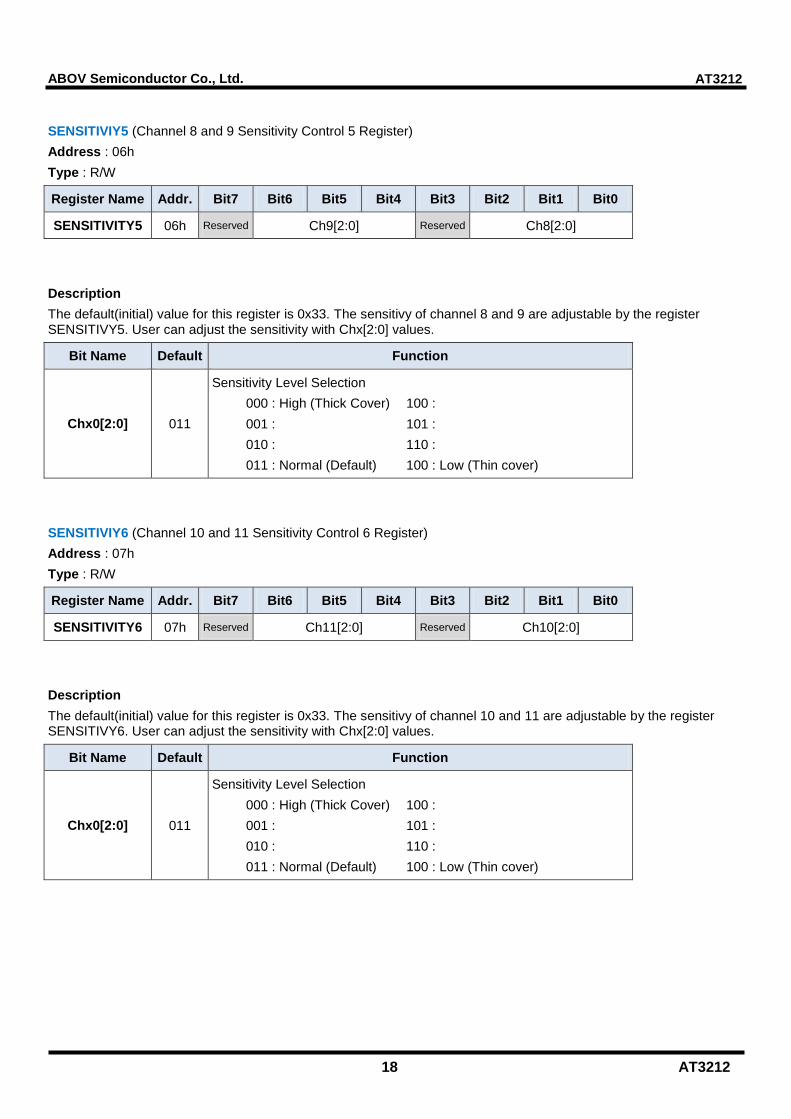
SENSITIVIY5 (Channel 8 and 9 Sensitivity Control 5 Register)
Address : 06h
Type : R/W
Register Name Addr. Bit7 Bit6 Bit5 Bit4 Bit3 Bit2 Bit1 Bit0
SENSITIVITY5 06h Reserved Ch9[2:0] Reserved Ch8[2:0]
Description
The default(initial) value for this register is 0x33. The sensitivy of channel 8 and 9 are adjustable by the register SENSITIVY5. User can adjust the sensitivity with Chx[2:0] values.
Bit Name Default Function
Chx0[2:0] 011
Sensitivity Level Selection
000 : High (Thick Cover) 100 :
001 : 101 :
010 : 110 :
011 : Normal (Default) 100 : Low (Thin cover)
SENSITIVIY6 (Channel 10 and 11 Sensitivity Control 6 Register)
Address : 07h
Type : R/W
Register Name Addr. Bit7 Bit6 Bit5 Bit4 Bit3 Bit2 Bit1 Bit0
SENSITIVITY6 07h Reserved Ch11[2:0] Reserved Ch10[2:0]
Description
The default(initial) value for this register is 0x33. The sensitivy of channel 10 and 11 are adjustable by the register SENSITIVY6. User can adjust the sensitivity with Chx[2:0] values.
Bit Name Default Function
Chx0[2:0] 011
Sensitivity Level Selection
000 : High (Thick Cover) 100 :
001 : 101 :
010 : 110 :
011 : Normal (Default) 100 : Low (Thin cover)
19 AT3212
AT3212 ABOV Semiconductor Co., Ltd.
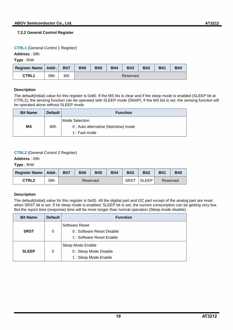
7.2.2 General Control Register
CTRL1 (General Control 1 Register)
Address : 08h
Type : R/W
Register Name Addr. Bit7 Bit6 Bit5 Bit4 Bit3 Bit2 Bit1 Bit0
CTRL1 08h MS Reserved
Description
The default(initial) value for this register is 0x80. If the MS bis is clear and if the sleep mode is enabled (SLEEP bit at CTRL2), the sensing function can be operated with SLEEP mode (SNAP). If the MS bis is set, the sensing function will be operated alone without SLEEP mode.
Bit Name Default Function
MS 80h
Mode Selection
0 : Auto alternative (fast/slow) mode
1 : Fast mode
CTRL2 (General Control 2 Register)
Address : 09h
Type : R/W
Register Name Addr. Bit7 Bit6 Bit5 Bit4 Bit3 Bit2 Bit1 Bit0
CTRL2 09h Reserved SRST SLEEP Reserved
Description
The default(initial) value for this register is 0x00. All the digitial part and I2C part except of the analog part are reset when SRST bit is set. If he sleep mode is enabled, SLEEP bit is set, the current consumption can be getting very low. But the report time (response) time will be more longer than normal operation (Sleep mode disable).
Bit Name Default Function
SRST 0
Software Reset
0 : Software Reset Disable
1 : Software Reset Enable
SLEEP 0
Sleep Mode Enable
0 : Sleep Mode Disable
1 : Sleep Mode Enable
20 AT3212
AT3212 ABOV Semiconductor Co., Ltd.
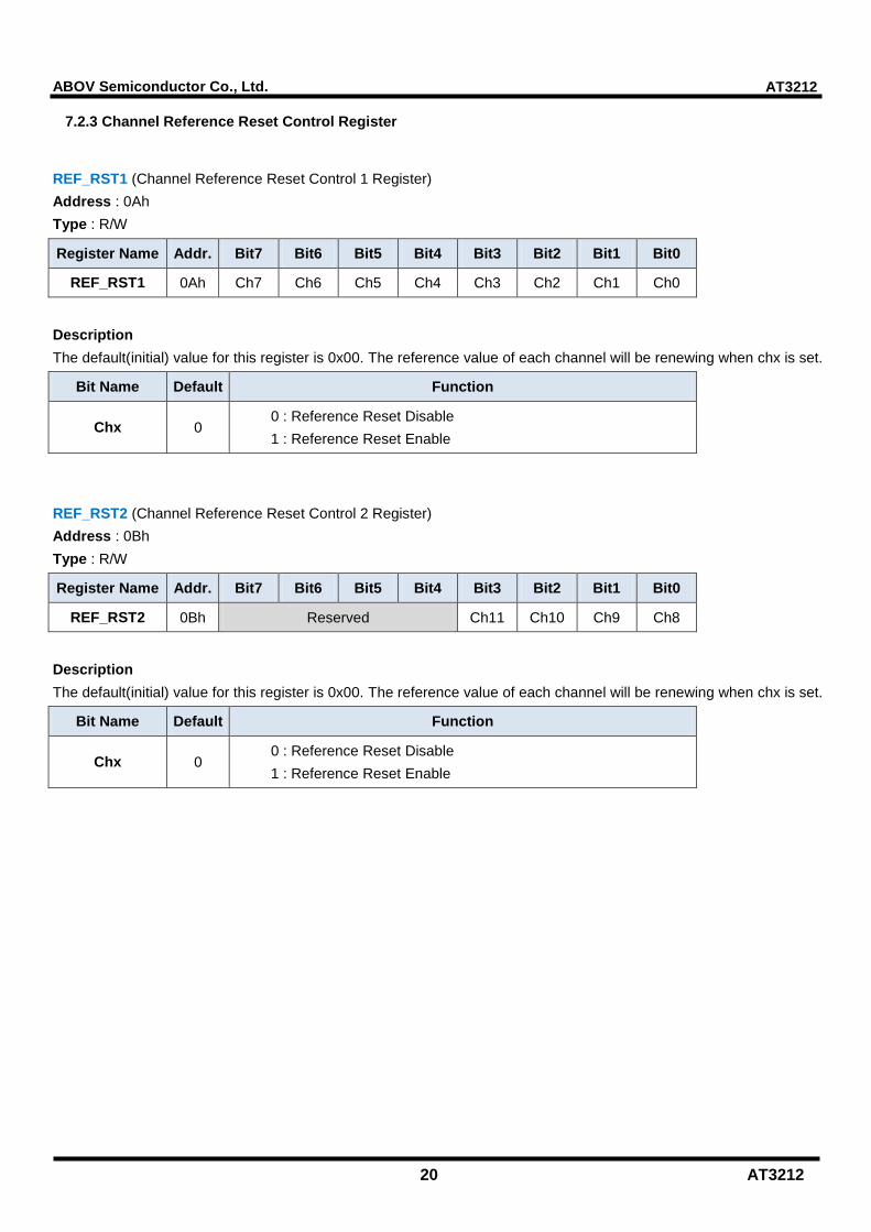
7.2.3 Channel Reference Reset Control Register
REF_RST1 (Channel Reference Reset Control 1 Register)
Address : 0Ah
Type : R/W
Register Name Addr. Bit7 Bit6 Bit5 Bit4 Bit3 Bit2 Bit1 Bit0
REF_RST1 0Ah Ch7 Ch6 Ch5 Ch4 Ch3 Ch2 Ch1 Ch0
Description
The default(initial) value for this register is 0x00. The reference value of each channel will be renewing when chx is set.
Bit Name Default Function
Chx 0 0 : Reference Reset Disable
1 : Reference Reset Enable
REF_RST2 (Channel Reference Reset Control 2 Register)
Address : 0Bh
Type : R/W
Register Name Addr. Bit7 Bit6 Bit5 Bit4 Bit3 Bit2 Bit1 Bit0
REF_RST2 0Bh Reserved Ch11 Ch10 Ch9 Ch8
Description
The default(initial) value for this register is 0x00. The reference value of each channel will be renewing when chx is set.
Bit Name Default Function
Chx 0 0 : Reference Reset Disable
1 : Reference Reset Enable
21 AT3212
AT3212 ABOV Semiconductor Co., Ltd.
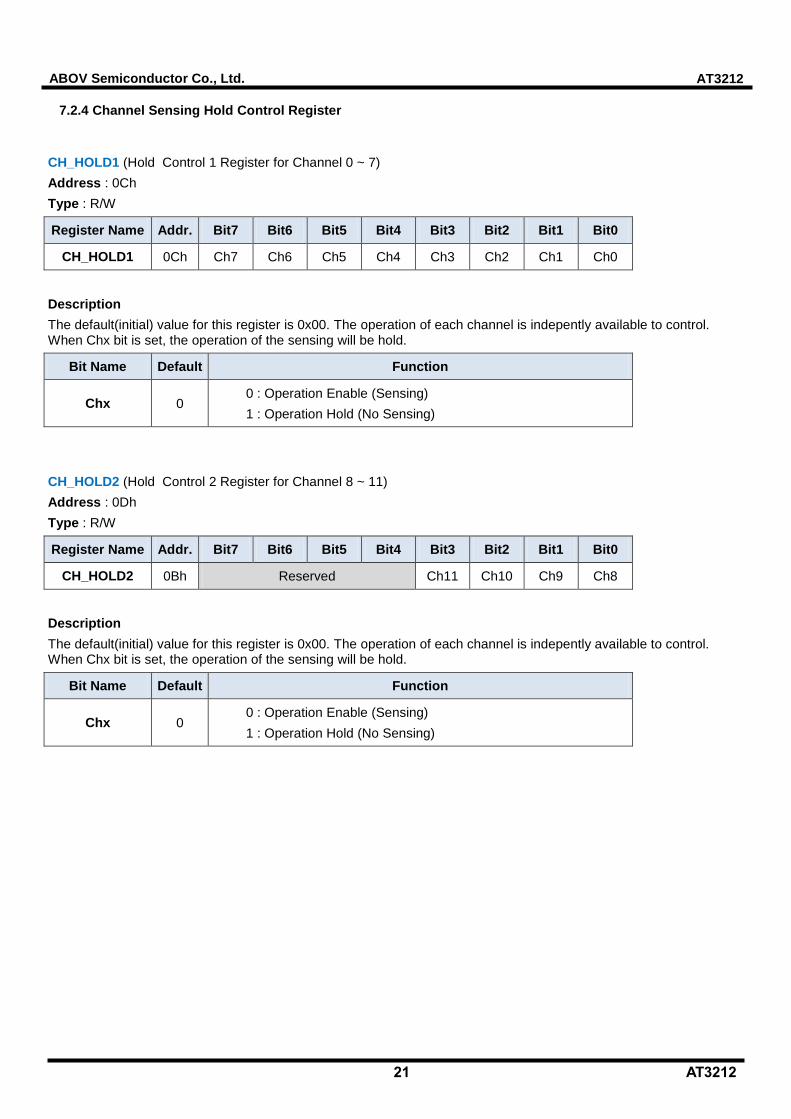
7.2.4 Channel Sensing Hold Control Register
CH_HOLD1 (Hold Control 1 Register for Channel 0 ~ 7)
Address : 0Ch
Type : R/W
Register Name Addr. Bit7 Bit6 Bit5 Bit4 Bit3 Bit2 Bit1 Bit0
CH_HOLD1 0Ch Ch7 Ch6 Ch5 Ch4 Ch3 Ch2 Ch1 Ch0
Description
The default(initial) value for this register is 0x00. The operation of each channel is indepently available to control. When Chx bit is set, the operation of the sensing will be hold.
Bit Name Default Function
Chx 0 0 : Operation Enable (Sensing)
1 : Operation Hold (No Sensing)
CH_HOLD2 (Hold Control 2 Register for Channel 8 ~ 11)
Address : 0Dh
Type : R/W
Register Name Addr. Bit7 Bit6 Bit5 Bit4 Bit3 Bit2 Bit1 Bit0
CH_HOLD2 0Bh Reserved Ch11 Ch10 Ch9 Ch8
Description
The default(initial) value for this register is 0x00. The operation of each channel is indepently available to control. When Chx bit is set, the operation of the sensing will be hold.
Bit Name Default Function
Chx 0 0 : Operation Enable (Sensing)
1 : Operation Hold (No Sensing)
22 AT3212
AT3212 ABOV Semiconductor Co., Ltd.
7.2.5 Channel Sensing Hold Control Register
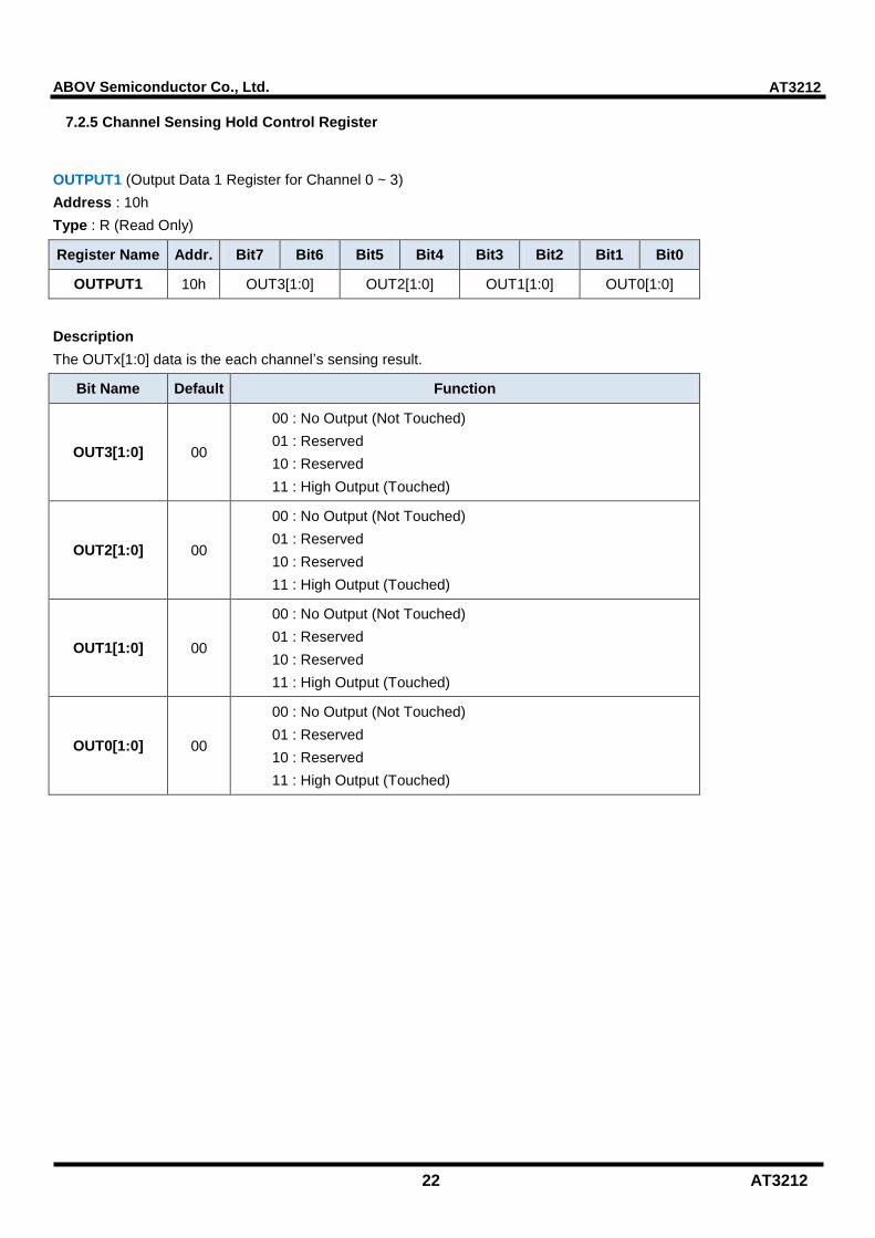
OUTPUT1 (Output Data 1 Register for Channel 0 ~ 3)
Address : 10h
Type : R (Read Only)
Register Name Addr. Bit7 Bit6 Bit5 Bit4 Bit3 Bit2 Bit1 Bit0
OUTPUT1 10h OUT3[1:0] OUT2[1:0] OUT1[1:0] OUT0[1:0]
Description
The OUTx[1:0] data is the each channel’s sensing result.
Bit Name Default Function
OUT3[1:0] 00
00 : No Output (Not Touched)
01 : Reserved
10 : Reserved
11 : High Output (Touched)
OUT2[1:0] 00
00 : No Output (Not Touched)
01 : Reserved
10 : Reserved
11 : High Output (Touched)
OUT1[1:0] 00
00 : No Output (Not Touched)
01 : Reserved
10 : Reserved
11 : High Output (Touched)
OUT0[1:0] 00
00 : No Output (Not Touched)
01 : Reserved
10 : Reserved
11 : High Output (Touched)

23 AT3212
AT3212 ABOV Semiconductor Co., Ltd.
OUTPUT2 (Output Data 1 Register for Channel 4 ~ 7)
Address : 11h
Type : R (Read Only)
Register Name Addr. Bit7 Bit6 Bit5 Bit4 Bit3 Bit2 Bit1 Bit0
OUTPUT2 11h OUT7[1:0] OUT6[1:0] OUT5[1:0] OUT4[1:0]
Description
The OUTx[1:0] data is the each channel’s sensing result.
Bit Name Default Function
OUT3[1:0] 00
00 : No Output (Not Touched)
01 : Reserved
10 : Reserved
11 : High Output (Touched)
OUT2[1:0] 00
00 : No Output (Not Touched)
01 : Reserved
10 : Reserved
11 : High Output (Touched)
OUT1[1:0] 00
00 : No Output (Not Touched)
01 : Reserved
10 : Reserved
11 : High Output (Touched)
OUT0[1:0] 00
00 : No Output (Not Touched)
01 : Reserved
10 : Reserved
11 : High Output (Touched)
24 AT3212
AT3212 ABOV Semiconductor Co., Ltd.
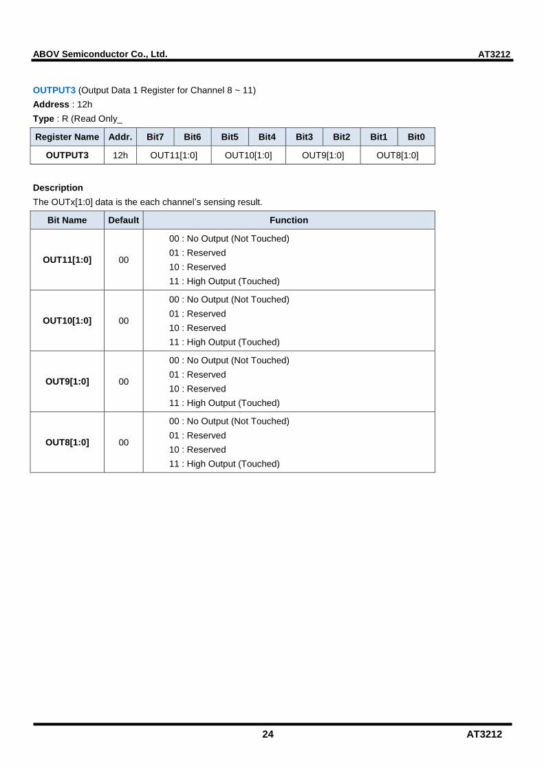
OUTPUT3 (Output Data 1 Register for Channel 8 ~ 11)
Address : 12h
Type : R (Read Only_
Register Name Addr. Bit7 Bit6 Bit5 Bit4 Bit3 Bit2 Bit1 Bit0
OUTPUT3 12h OUT11[1:0] OUT10[1:0] OUT9[1:0] OUT8[1:0]
Description
The OUTx[1:0] data is the each channel’s sensing result.
Bit Name Default Function
OUT11[1:0] 00
00 : No Output (Not Touched)
01 : Reserved
10 : Reserved
11 : High Output (Touched)
OUT10[1:0] 00
00 : No Output (Not Touched)
01 : Reserved
10 : Reserved
11 : High Output (Touched)
OUT9[1:0] 00
00 : No Output (Not Touched)
01 : Reserved
10 : Reserved
11 : High Output (Touched)
OUT8[1:0] 00
00 : No Output (Not Touched)
01 : Reserved
10 : Reserved
11 : High Output (Touched)
25 AT3212
AT3212 ABOV Semiconductor Co., Ltd.
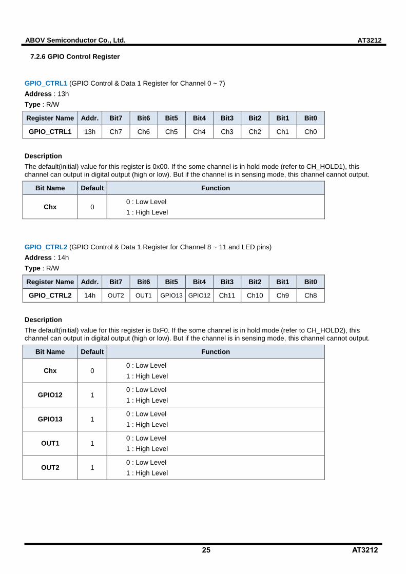
7.2.6 GPIO Control Register
GPIO_CTRL1 (GPIO Control & Data 1 Register for Channel 0 ~ 7)
Address : 13h
Type : R/W
Register Name Addr. Bit7 Bit6 Bit5 Bit4 Bit3 Bit2 Bit1 Bit0
GPIO_CTRL1 13h Ch7 Ch6 Ch5 Ch4 Ch3 Ch2 Ch1 Ch0
Description
The default(initial) value for this register is 0x00. If the some channel is in hold mode (refer to CH_HOLD1), this channel can output in digital output (high or low). But if the channel is in sensing mode, this channel cannot output.
Bit Name Default Function
Chx 0 0 : Low Level
1 : High Level
GPIO_CTRL2 (GPIO Control & Data 1 Register for Channel 8 ~ 11 and LED pins)
Address : 14h
Type : R/W
Register Name Addr. Bit7 Bit6 Bit5 Bit4 Bit3 Bit2 Bit1 Bit0
GPIO_CTRL2 14h OUT2 OUT1 GPIO13 GPIO12 Ch11 Ch10 Ch9 Ch8
Description
The default(initial) value for this register is 0xF0. If the some channel is in hold mode (refer to CH_HOLD2), this channel can output in digital output (high or low). But if the channel is in sensing mode, this channel cannot output.
Bit Name Default Function
Chx 0 0 : Low Level
1 : High Level
GPIO12 1 0 : Low Level
1 : High Level
GPIO13 1 0 : Low Level
1 : High Level
OUT1 1 0 : Low Level
1 : High Level
OUT2 1 0 : Low Level
1 : High Level
26 AT3212
AT3212 ABOV Semiconductor Co., Ltd.
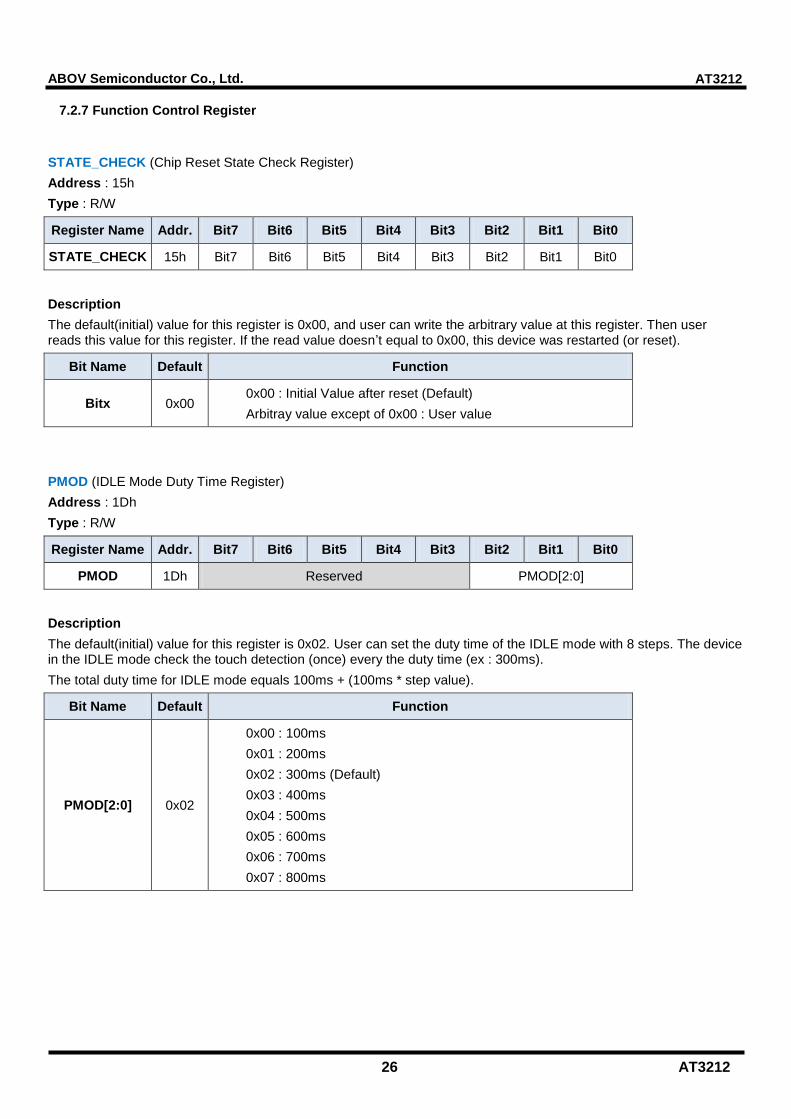
7.2.7 Function Control Register
STATE_CHECK (Chip Reset State Check Register)
Address : 15h
Type : R/W
Register Name Addr. Bit7 Bit6 Bit5 Bit4 Bit3 Bit2 Bit1 Bit0
STATE_CHECK 15h Bit7 Bit6 Bit5 Bit4 Bit3 Bit2 Bit1 Bit0
Description
The default(initial) value for this register is 0x00, and user can write the arbitrary value at this register. Then user reads this value for this register. If the read value doesn’t equal to 0x00, this device was restarted (or reset).
Bit Name Default Function
Bitx 0x00 0x00 : Initial Value after reset (Default)
Arbitray value except of 0x00 : User value
PMOD (IDLE Mode Duty Time Register)
Address : 1Dh
Type : R/W
Register Name Addr. Bit7 Bit6 Bit5 Bit4 Bit3 Bit2 Bit1 Bit0
PMOD 1Dh Reserved PMOD[2:0]
Description
The default(initial) value for this register is 0x02. User can set the duty time of the IDLE mode with 8 steps. The device in the IDLE mode check the touch detection (once) every the duty time (ex : 300ms).
The total duty time for IDLE mode equals 100ms + (100ms * step value).
Bit Name Default Function
PMOD[2:0] 0x02
0x00 : 100ms
0x01 : 200ms
0x02 : 300ms (Default)
0x03 : 400ms
0x04 : 500ms
0x05 : 600ms
0x06 : 700ms
0x07 : 800ms
27 AT3212
AT3212 ABOV Semiconductor Co., Ltd.
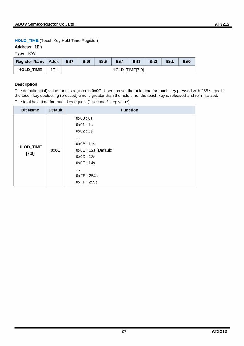
HOLD_TIME (Touch Key Hold Time Register)
Address : 1Eh
Type : R/W
Register Name Addr. Bit7 Bit6 Bit5 Bit4 Bit3 Bit2 Bit1 Bit0
HOLD_TIME 1Eh HOLD_TIME[7:0]
Description
The default(initial) value for this register is 0x0C. User can set the hold time for touch key pressed with 255 steps. If the touch key dectecting (pressed) time is greater than the hold time, the touch key is released and re-initialized.
The total hold time for touch key equals (1 second * step value).
Bit Name Default Function
HLOD_TIME
[7:0] 0x0C
0x00 : 0s
0x01 : 1s
0x02 : 2s
…
0x0B : 11s
0x0C : 12s (Default)
0x0D : 13s
0x0E : 14s
…
0xFE : 254s
0xFF : 255s
28 AT3212
AT3212 ABOV Semiconductor Co., Ltd.
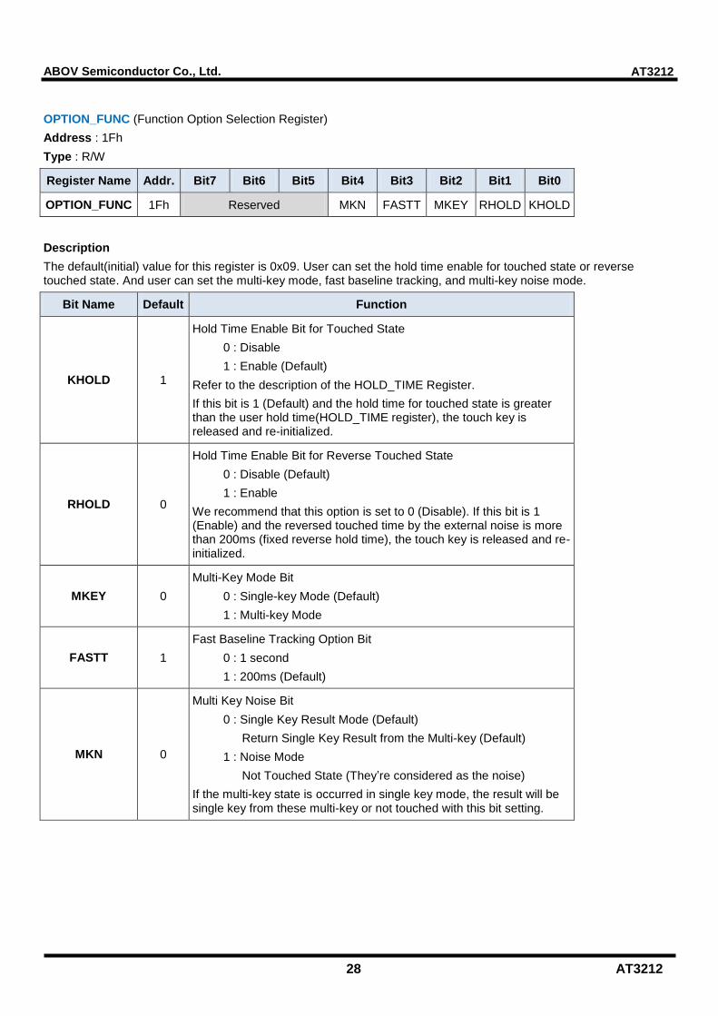
OPTION_FUNC (Function Option Selection Register)
Address : 1Fh
Type : R/W
Register Name Addr. Bit7 Bit6 Bit5 Bit4 Bit3 Bit2 Bit1 Bit0
OPTION_FUNC 1Fh Reserved MKN FASTT MKEY RHOLD KHOLD
Description
The default(initial) value for this register is 0x09. User can set the hold time enable for touched state or reverse touched state. And user can set the multi-key mode, fast baseline tracking, and multi-key noise mode.
Bit Name Default Function
KHOLD 1
Hold Time Enable Bit for Touched State
0 : Disable
1 : Enable (Default)
Refer to the description of the HOLD_TIME Register.
If this bit is 1 (Default) and the hold time for touched state is greater than the user hold time(HOLD_TIME register), the touch key is released and re-initialized.
RHOLD 0
Hold Time Enable Bit for Reverse Touched State
0 : Disable (Default)
1 : Enable
We recommend that this option is set to 0 (Disable). If this bit is 1 (Enable) and the reversed touched time by the external noise is more than 200ms (fixed reverse hold time), the touch key is released and re-initialized.
MKEY 0
Multi-Key Mode Bit
0 : Single-key Mode (Default)
1 : Multi-key Mode
FASTT 1
Fast Baseline Tracking Option Bit
0 : 1 second
1 : 200ms (Default)
MKN 0
Multi Key Noise Bit
0 : Single Key Result Mode (Default)
Return Single Key Result from the Multi-key (Default)
1 : Noise Mode
Not Touched State (They’re considered as the noise)
If the multi-key state is occurred in single key mode, the result will be single key from these multi-key or not touched with this bit setting.
29 AT3212
AT3212 ABOV Semiconductor Co., Ltd.
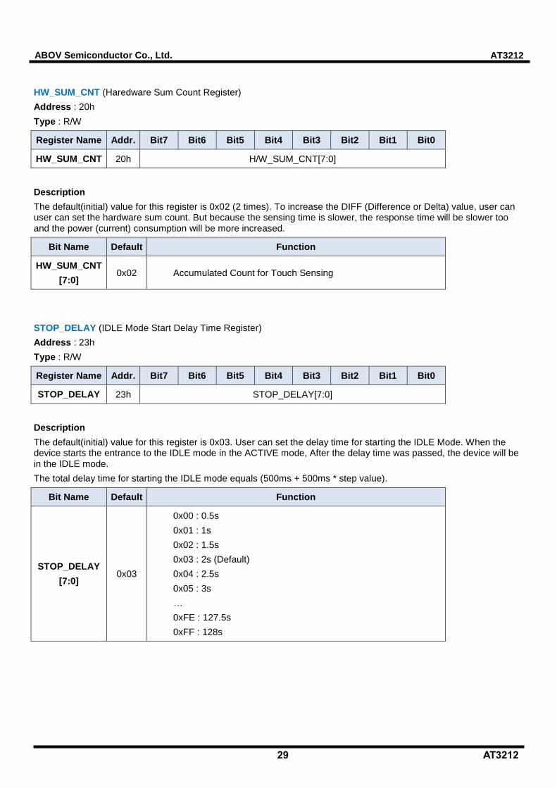
HW_SUM_CNT (Haredware Sum Count Register)
Address : 20h
Type : R/W
Register Name Addr. Bit7 Bit6 Bit5 Bit4 Bit3 Bit2 Bit1 Bit0
HW_SUM_CNT 20h H/W_SUM_CNT[7:0]
Description
The default(initial) value for this register is 0x02 (2 times). To increase the DIFF (Difference or Delta) value, user can user can set the hardware sum count. But because the sensing time is slower, the response time will be slower too and the power (current) consumption will be more increased.
Bit Name Default Function
HW_SUM_CNT
[7:0] 0x02 Accumulated Count for Touch Sensing
STOP_DELAY (IDLE Mode Start Delay Time Register)
Address : 23h
Type : R/W
Register Name Addr. Bit7 Bit6 Bit5 Bit4 Bit3 Bit2 Bit1 Bit0
STOP_DELAY 23h STOP_DELAY[7:0]
Description
The default(initial) value for this register is 0x03. User can set the delay time for starting the IDLE Mode. When the device starts the entrance to the IDLE mode in the ACTIVE mode, After the delay time was passed, the device will be in the IDLE mode.
The total delay time for starting the IDLE mode equals (500ms + 500ms * step value).
Bit Name Default Function
STOP_DELAY
[7:0] 0x03
0x00 : 0.5s
0x01 : 1s
0x02 : 1.5s
0x03 : 2s (Default)
0x04 : 2.5s
0x05 : 3s
…
0xFE : 127.5s
0xFF : 128s
30 AT3212
AT3212 ABOV Semiconductor Co., Ltd.
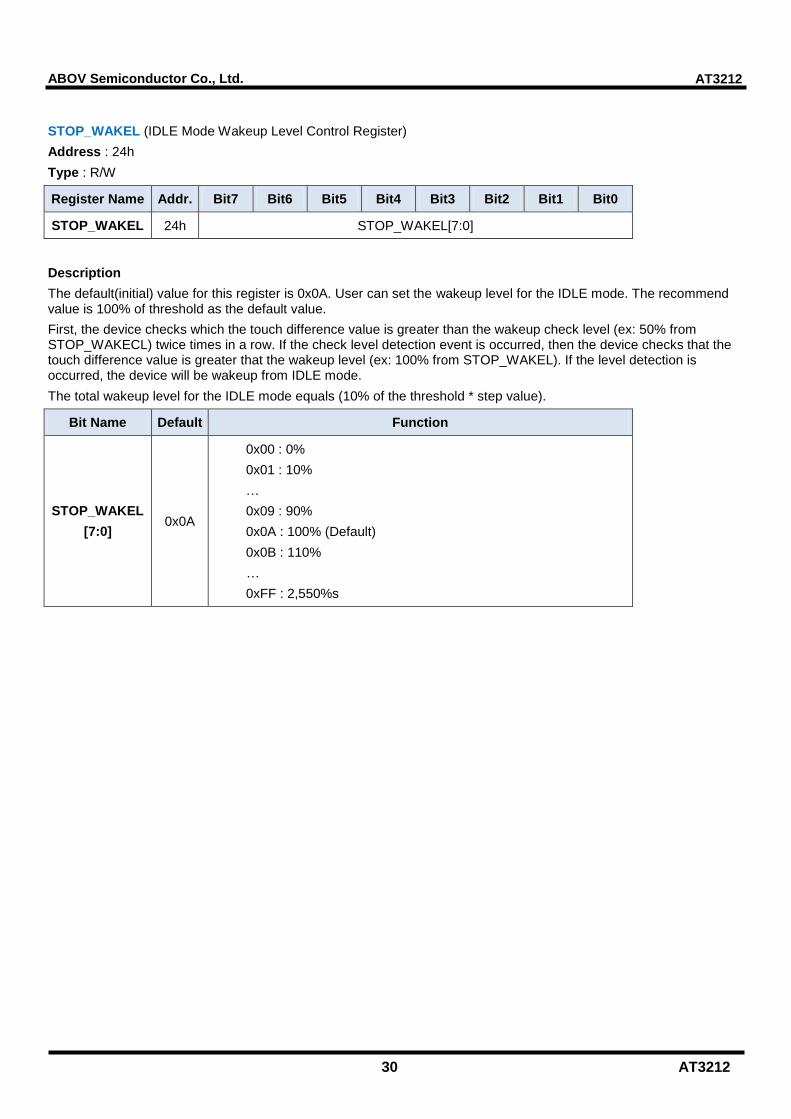
STOP_WAKEL (IDLE Mode Wakeup Level Control Register)
Address : 24h
Type : R/W
Register Name Addr. Bit7 Bit6 Bit5 Bit4 Bit3 Bit2 Bit1 Bit0
STOP_WAKEL 24h STOP_WAKEL[7:0]
Description
The default(initial) value for this register is 0x0A. User can set the wakeup level for the IDLE mode. The recommend value is 100% of threshold as the default value.
First, the device checks which the touch difference value is greater than the wakeup check level (ex: 50% from STOP_WAKECL) twice times in a row. If the check level detection event is occurred, then the device checks that the touch difference value is greater that the wakeup level (ex: 100% from STOP_WAKEL). If the level detection is occurred, the device will be wakeup from IDLE mode.
The total wakeup level for the IDLE mode equals (10% of the threshold * step value).
Bit Name Default Function
STOP_WAKEL
[7:0] 0x0A
0x00 : 0%
0x01 : 10%
…
0x09 : 90%
0x0A : 100% (Default)
0x0B : 110%
…
0xFF : 2,550%s
31 AT3212
AT3212 ABOV Semiconductor Co., Ltd.
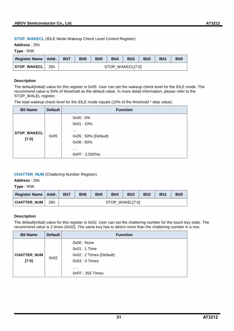
STOP_WAKECL (IDLE Mode Wakeup Check Level Control Register)
Address : 25h
Type : R/W
Register Name Addr. Bit7 Bit6 Bit5 Bit4 Bit3 Bit2 Bit1 Bit0
STOP_WAKECL 25h STOP_WAKECL[7:0]
Description
The default(initial) value for this register is 0x05. User can set the wakeup check level for the IDLE mode. The recommend value is 50% of threshold as the default value. In more detail information, please refer to the STOP_WALEL register.
The total wakeup check level for the IDLE mode equals (10% of the threshold * step value).
Bit Name Default Function
STOP_WAKECL
[7:0] 0x05
0x00 : 0%
0x01 : 10%
…
0x05 : 50% (Default)
0x06 : 60%
…
0xFF : 2,550%s
CHATTER_NUM (Chattering Number Register)
Address : 26h
Type : R/W
Register Name Addr. Bit7 Bit6 Bit5 Bit4 Bit3 Bit2 Bit1 Bit0
CHATTER_NUM 26h STOP_WAKEL[7:0]
Description
The default(initial) value for this register is 0x02. User can set the chattering number for the touch key state. The recommend value is 2 times (0x02). The same key has to detect more than the chattering number in a row.
Bit Name Default Function
CHATTER_NUM
[7:0] 0x02
0x00 : None
0x01 : 1 Time
0x02 : 2 Times (Default)
0x03 : 3 Times
…
0xFF : 255 Times
32 AT3212
AT3212 ABOV Semiconductor Co., Ltd.
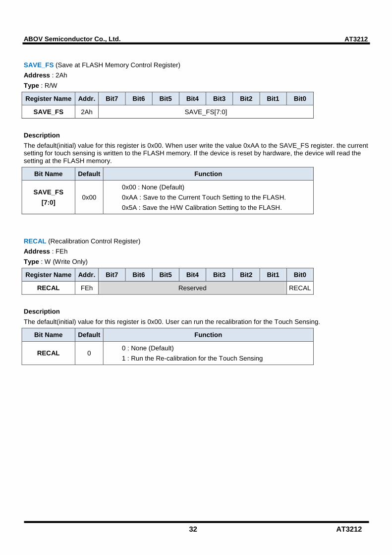
SAVE_FS (Save at FLASH Memory Control Register)
Address : 2Ah
Type : R/W
Register Name Addr. Bit7 Bit6 Bit5 Bit4 Bit3 Bit2 Bit1 Bit0
SAVE_FS 2Ah SAVE_FS[7:0]
Description
The default(initial) value for this register is 0x00. When user write the value 0xAA to the SAVE_FS register. the current setting for touch sensing is written to the FLASH memory. If the device is reset by hardware, the device will read the setting at the FLASH memory.
Bit Name Default Function
SAVE_FS
[7:0] 0x00
0x00 : None (Default)
0xAA : Save to the Current Touch Setting to the FLASH.
0x5A : Save the H/W Calibration Setting to the FLASH.
RECAL (Recalibration Control Register)
Address : FEh
Type : W (Write Only)
Register Name Addr. Bit7 Bit6 Bit5 Bit4 Bit3 Bit2 Bit1 Bit0
RECAL FEh Reserved RECAL
Description
The default(initial) value for this register is 0x00. User can run the recalibration for the Touch Sensing.
Bit Name Default Function
RECAL 0 0 : None (Default)
1 : Run the Re-calibration for the Touch Sensing
33 AT3212
AT3212 ABOV Semiconductor Co., Ltd.
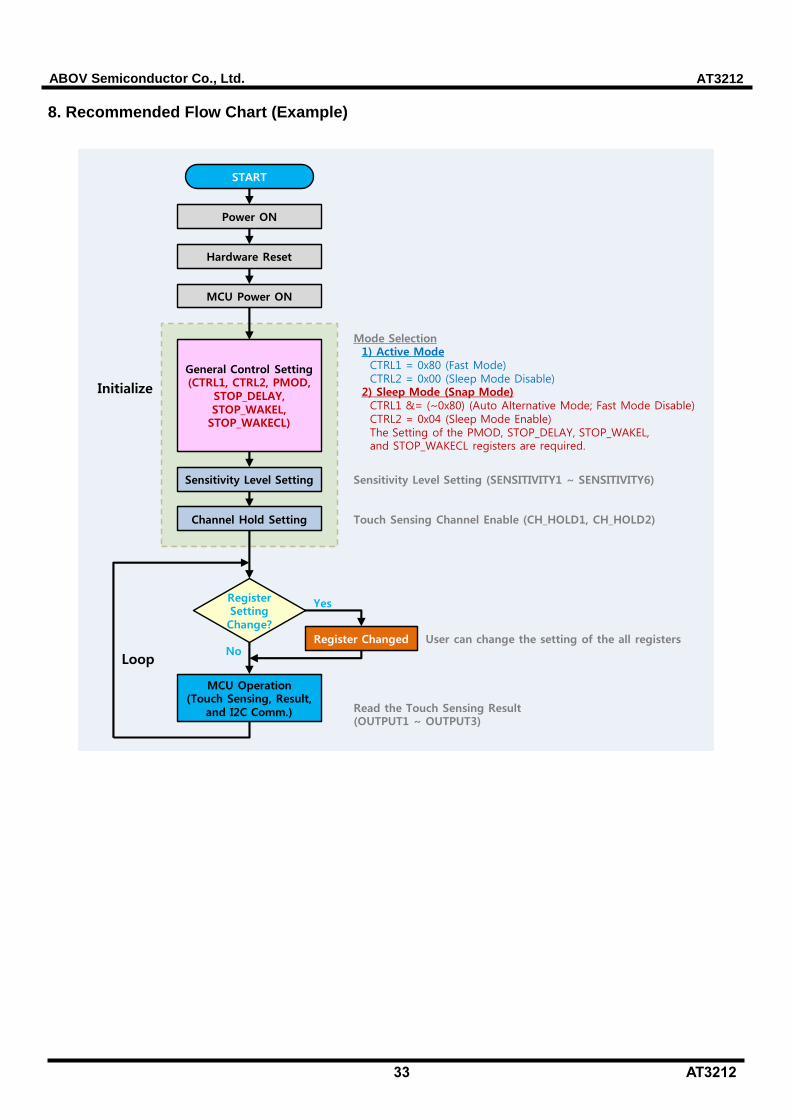
8. Recommended Flow Chart (Example)
Touch Sensing Channel Enable (CH_HOLD1, CH_HOLD2)
START
Power ON
Hardware Reset
MCU Power ON
General Control Setting(CTRL1, CTRL2, PMOD,
STOP_DELAY,STOP_WAKEL,
STOP_WAKECL)
Sensitivity Level Setting
Channel Hold Setting
Sensitivity Level Setting (SENSITIVITY1 ~ SENSITIVITY6)
Register Changed
Yes
No
MCU Operation(Touch Sensing, Result,
and I2C Comm.) Read the Touch Sensing Result(OUTPUT1 ~ OUTPUT3)
Loop
User can change the setting of the all registers
RegisterSettingChange?
Mode Selection1) Active Mode
CTRL1 = 0x80 (Fast Mode)CTRL2 = 0x00 (Sleep Mode Disable)
2) Sleep Mode (Snap Mode)CTRL1 &= (~0x80) (Auto Alternative Mode; Fast Mode Disable)CTRL2 = 0x04 (Sleep Mode Enable)The Setting of the PMOD, STOP_DELAY, STOP_WAKEL,and STOP_WAKECL registers are required.
Initialize
34 AT3212
AT3212 ABOV Semiconductor Co., Ltd.
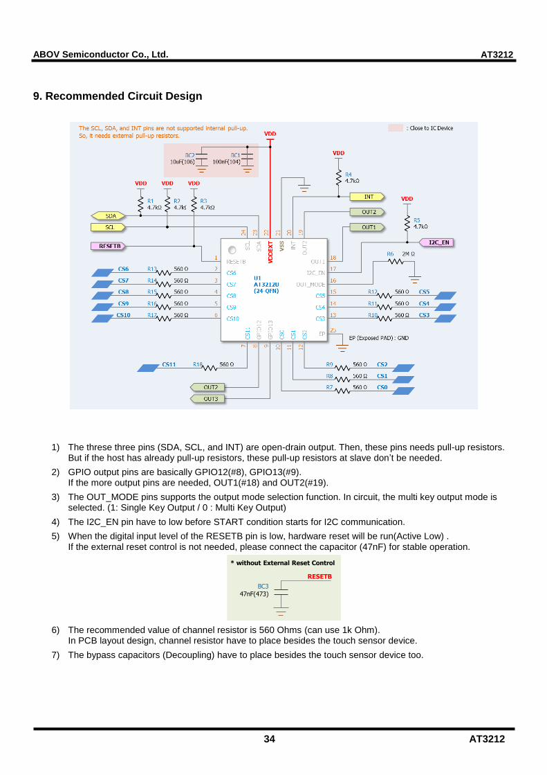
9. Recommended Circuit Design
1) The threse three pins (SDA, SCL, and INT) are open-drain output. Then, these pins needs pull-up resistors. But if the host has already pull-up resistors, these pull-up resistors at slave don’t be needed.
2) GPIO output pins are basically GPIO12(#8), GPIO13(#9). If the more output pins are needed, OUT1(#18) and OUT2(#19).
3) The OUT_MODE pins supports the output mode selection function. In circuit, the multi key output mode is selected. (1: Single Key Output / 0 : Multi Key Output)
4) The I2C_EN pin have to low before START condition starts for I2C communication.
5) When the digital input level of the RESETB pin is low, hardware reset will be run(Active Low) . If the external reset control is not needed, please connect the capacitor (47nF) for stable operation.
BC347nF(473)
RESETB
* without External Reset Control
6) The recommended value of channel resistor is 560 Ohms (can use 1k Ohm). In PCB layout design, channel resistor have to place besides the touch sensor device.
7) The bypass capacitors (Decoupling) have to place besides the touch sensor device too.
35 AT3212
AT3212 ABOV Semiconductor Co., Ltd.
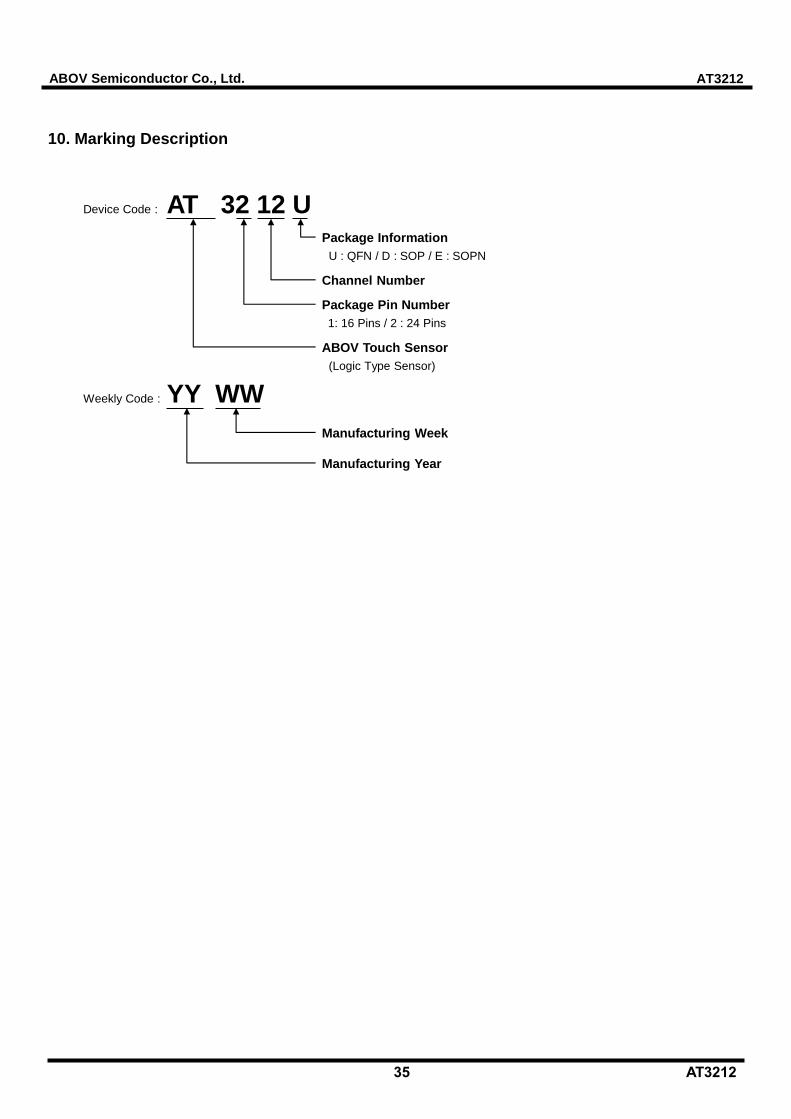
10. Marking Description
Device Code : AT 32 12 UPackage Information
U : QFN / D : SOP / E : SOPN
Channel Number
ABOV Touch Sensor
(Logic Type Sensor)
Weekly Code : YY WW
Manufacturing Week
Manufacturing Year
Package Pin Number
1: 16 Pins / 2 : 24 Pins