Embed Size (px)
Citation preview
Single and Dual, Ultralow Distortion, Ultralow Noise Op Amps
AD8597/AD8599
Rev. C Information furnished by Analog Devices is believed to be accurate and reliable. However, no responsibility is assumed by Analog Devices for its use, nor for any infringements of patents or other rights of third parties that may result from its use. Specifications subject to change without notice. No license is granted by implication or otherwise under any patent or patent rights of Analog Devices. Trademarks and registered trademarks are the property of their respective owners.
One Technology Way, P.O. Box 9106, Norwood, MA 02062-9106, U.S.A.Tel: 781.329.4700 www.analog.com Fax: 781.461.3113 ©2007–2009 Analog Devices, Inc. All rights reserved.
FEATURES Low noise: 1.1 nV/√Hz at 1 kHz Low distortion: −120 dB THD @ 1 kHz Input noise, 0.1 Hz to 10 Hz: <76 nV p-p Slew rate: 14 V/μs Wide bandwidth: 10 MHz Supply current: 4.8 mA/amp typical Low offset voltage: 10 μV typical CMRR: 120 dB Unity-gain stable ±15 V operation
APPLICATIONS Professional audio preamplifiers ATE/precision testers Imaging systems Medical/physiological measurements Precision detectors/instruments Precision data conversion
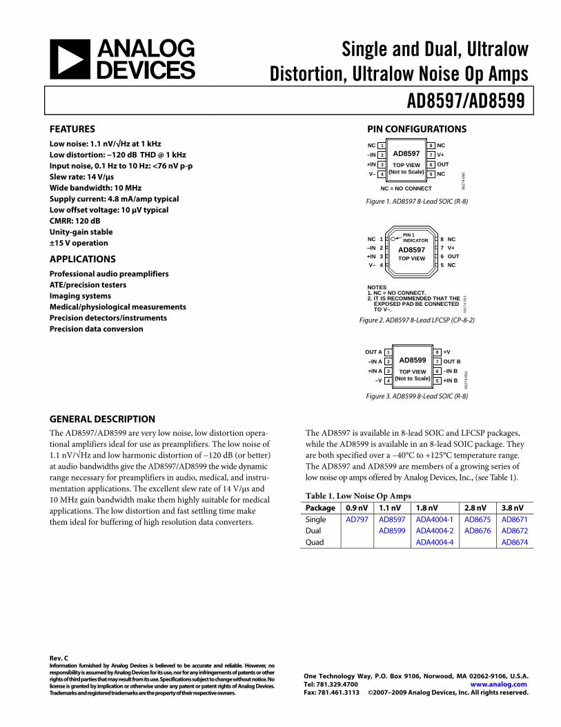
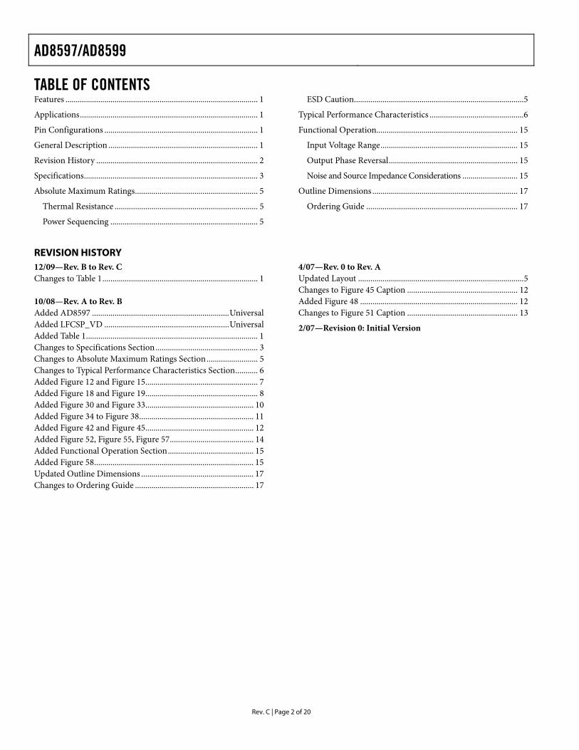
PIN CONFIGURATIONS
0627
4-06
0
NC 1
–IN 2
+IN 3
V– 4
NC8
V+7
OUT6
NC5
NC = NO CONNECT
AD8597TOP VIEW
(Not to Scale)
Figure 1. AD8597 8-Lead SOIC (R-8)
PIN 1INDICATOR1
234
NC–IN+INV–
7 V+8 NC
6 OUT5 NC
TOP VIEW
0627
4-06
1
AD8597
NOTES1. NC = NO CONNECT.2. IT IS RECOMMENDED THAT THE EXPOSED PAD BE CONNECTED TO V–.
Figure 2. AD8597 8-Lead LFCSP (CP-8-2)
OUT A 1
–IN A 2
+IN A 3
–V 4
+V8
OUT B7
–IN B6
+IN B5
AD8599TOP VIEW
(Not to Scale)
0627
4-05
4
Figure 3. AD8599 8-Lead SOIC (R-8)
GENERAL DESCRIPTION The AD8597/AD8599 are very low noise, low distortion opera-tional amplifiers ideal for use as preamplifiers. The low noise of 1.1 nV/√Hz and low harmonic distortion of −120 dB (or better) at audio bandwidths give the AD8597/AD8599 the wide dynamic range necessary for preamplifiers in audio, medical, and instru-mentation applications. The excellent slew rate of 14 V/μs and 10 MHz gain bandwidth make them highly suitable for medical applications. The low distortion and fast settling time make them ideal for buffering of high resolution data converters.
The AD8597 is available in 8-lead SOIC and LFCSP packages, while the AD8599 is available in an 8-lead SOIC package. They are both specified over a −40°C to +125°C temperature range. The AD8597 and AD8599 are members of a growing series of low noise op amps offered by Analog Devices, Inc., (see Table 1).
Table 1. Low Noise Op Amps Package 0.9 nV 1.1 nV 1.8 nV 2.8 nV 3.8 nV Single AD797 AD8597 ADA4004-1 AD8675 AD8671 Dual AD8599 ADA4004-2 AD8676 AD8672 Quad ADA4004-4 AD8674
AD8597/AD8599
Rev. C | Page 2 of 20
TABLE OF CONTENTS Features .............................................................................................. 1
Applications ....................................................................................... 1
Pin Configurations ........................................................................... 1
General Description ......................................................................... 1
Revision History ............................................................................... 2
Specifications ..................................................................................... 3
Absolute Maximum Ratings ............................................................ 5
Thermal Resistance ...................................................................... 5
Power Sequencing ........................................................................ 5
ESD Caution...................................................................................5
Typical Performance Characteristics ..............................................6
Functional Operation..................................................................... 15
Input Voltage Range ................................................................... 15
Output Phase Reversal ............................................................... 15
Noise and Source Impedance Considerations ........................... 15
Outline Dimensions ....................................................................... 17
Ordering Guide .......................................................................... 17
REVISION HISTORY 12/09—Rev. B to Rev. C Changes to Table 1 ............................................................................ 1 10/08—Rev. A to Rev. B Added AD8597 ................................................................... Universal Added LFCSP_VD ............................................................. Universal Added Table 1 .................................................................................... 1 Changes to Specifications Section .................................................. 3 Changes to Absolute Maximum Ratings Section ......................... 5 Changes to Typical Performance Characteristics Section ........... 6 Added Figure 12 and Figure 15....................................................... 7 Added Figure 18 and Figure 19....................................................... 8 Added Figure 30 and Figure 33..................................................... 10 Added Figure 34 to Figure 38 ........................................................ 11 Added Figure 42 and Figure 45..................................................... 12 Added Figure 52, Figure 55, Figure 57 ......................................... 14 Added Functional Operation Section .......................................... 15 Added Figure 58 .............................................................................. 15 Updated Outline Dimensions ....................................................... 17 Changes to Ordering Guide .......................................................... 17
4/07—Rev. 0 to Rev. A Updated Layout ................................................................................. 5 Changes to Figure 45 Caption ...................................................... 12 Added Figure 48 ............................................................................. 12 Changes to Figure 51 Caption ...................................................... 13
2/07—Revision 0: Initial Version
AD8597/AD8599
Rev. C | Page 3 of 20
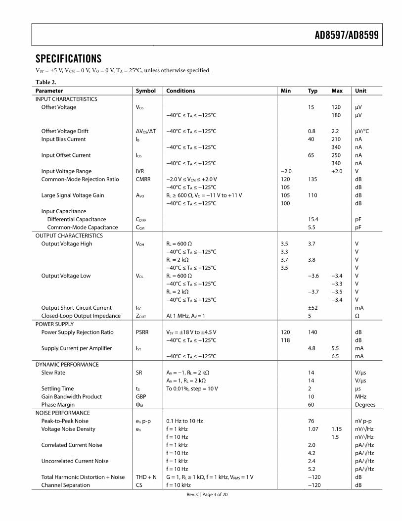
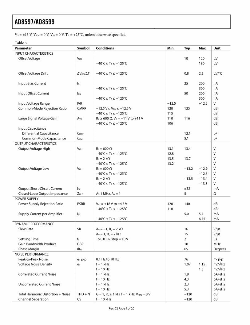
SPECIFICATIONS VSY = ±5 V, VCM = 0 V, VO = 0 V, TA = 25°C, unless otherwise specified.
Table 2. Parameter Symbol Conditions Min Typ Max Unit INPUT CHARACTERISTICS
Offset Voltage VOS 15 120 μV −40°C ≤ TA ≤ +125°C 180 μV Offset Voltage Drift ΔVOS/ΔT −40°C ≤ TA ≤ +125°C 0.8 2.2 μV/°C Input Bias Current IB 40 210 nA −40°C ≤ TA ≤ +125°C 340 nA Input Offset Current IOS 65 250 nA −40°C ≤ TA ≤ +125°C 340 nA Input Voltage Range IVR −2.0 +2.0 V Common-Mode Rejection Ratio CMRR −2.0 V ≤ VCM ≤ +2.0 V 120 135 dB −40°C ≤ TA ≤ +125°C 105 dB Large Signal Voltage Gain AVO RL ≥ 600 Ω, VO = −11 V to +11 V 105 110 dB −40°C ≤ TA ≤ +125°C 100 dB Input Capacitance
Differential Capacitance CDIFF 15.4 pF Common-Mode Capacitance CCM 5.5 pF
OUTPUT CHARACTERISTICS Output Voltage High VOH RL = 600 Ω 3.5 3.7 V −40°C ≤ TA ≤ +125°C 3.3 V RL = 2 kΩ 3.7 3.8 V −40°C ≤ TA ≤ +125°C 3.5 V Output Voltage Low VOL RL = 600 Ω −3.6 −3.4 V −40°C ≤ TA ≤ +125°C −3.3 V RL = 2 kΩ −3.7 −3.5 V −40°C ≤ TA ≤ +125°C −3.4 V Output Short-Circuit Current ISC ±52 mA Closed-Loop Output Impedance ZOUT At 1 MHz, AV = 1 5 Ω
POWER SUPPLY Power Supply Rejection Ratio PSRR VSY = ±18 V to ±4.5 V 120 140 dB −40°C ≤ TA ≤ +125°C 118 dB Supply Current per Amplifier ISY 4.8 5.5 mA −40°C ≤ TA ≤ +125°C 6.5 mA
DYNAMIC PERFORMANCE Slew Rate SR AV = −1, RL = 2 kΩ 14 V/μs AV = 1, RL = 2 kΩ 14 V/μs Settling Time tS To 0.01%, step = 10 V 2 μs Gain Bandwidth Product GBP 10 MHz Phase Margin ΦM 60 Degrees
NOISE PERFORMANCE Peak-to-Peak Noise en p-p 0.1 Hz to 10 Hz 76 nV p-p Voltage Noise Density en f = 1 kHz 1.07 1.15 nV/√Hz f = 10 Hz 1.5 nV/√Hz Correlated Current Noise f = 1 kHz 2.0 pA/√Hz f = 10 Hz 4.2 pA/√Hz Uncorrelated Current Noise f = 1 kHz 2.4 pA/√Hz f = 10 Hz 5.2 pA/√Hz Total Harmonic Distortion + Noise THD + N G = 1, RL ≥ 1 kΩ, f = 1 kHz, VRMS = 1 V −120 dB Channel Separation CS f = 10 kHz −120 dB
AD8597/AD8599
Rev. C | Page 4 of 20
VS = ±15 V, VCM = 0 V, VO = 0 V, TA = +25°C, unless otherwise specified.
Table 3. Parameter Symbol Conditions Min Typ Max Unit INPUT CHARACTERISTICS
Offset Voltage VOS 10 120 μV −40°C ≤ TA ≤ +125°C 180 μV Offset Voltage Drift ΔVOS/ΔT −40°C ≤ TA ≤ +125°C 0.8 2.2 μV/°C Input Bias Current IB 25 200 nA −40°C ≤ TA ≤ +125°C 300 nA Input Offset Current IOS 50 200 nA −40°C ≤ TA ≤ +125°C 300 nA Input Voltage Range IVR −12.5 +12.5 V Common-Mode Rejection Ratio CMRR −12.5 V ≤ VCM ≤ +12.5 V 120 135 dB −40°C ≤ TA ≤ +125°C 115 dB Large Signal Voltage Gain AVO RL ≥ 600 Ω, VO = −11 V to +11 V 110 116 dB −40°C ≤ TA ≤ +125°C 106 dB Input Capacitance
Differential Capacitance CDIFF 12.1 pF Common-Mode Capacitance CCM 5.1 pF
OUTPUT CHARACTERISTICS Output Voltage High VOH RL = 600 Ω 13.1 13.4 V −40°C ≤ TA ≤ +125°C 12.8 V RL = 2 kΩ 13.5 13.7 V −40°C ≤ TA ≤ +125°C 13.2 V Output Voltage Low VOL RL = 600 Ω −13.2 −12.9 V −40°C ≤ TA ≤ +125°C −12.8 V RL = 2 kΩ −13.5 −13.4 V −40°C ≤ TA ≤ +125°C −13.3 V Output Short-Circuit Current ISC ±52 mA Closed-Loop Output Impedance ZOUT At 1 MHz, AV = 1 5 Ω
POWER SUPPLY Power Supply Rejection Ratio PSRR VSY = ±18 V to ±4.5 V 120 140 dB −40°C ≤ TA ≤ +125°C 118 dB Supply Current per Amplifier ISY 5.0 5.7 mA −40°C ≤ TA ≤ +125°C 6.75 mA
DYNAMIC PERFORMANCE Slew Rate SR AV = −1, RL = 2 kΩ 16 V/μs AV = 1, RL = 2 kΩ 15 V/μs Settling Time ts To 0.01%, step = 10 V 2 μs Gain Bandwidth Product GBP 10 MHz Phase Margin ΦM 65 Degrees
NOISE PERFORMANCE Peak-to-Peak Noise en p-p 0.1 Hz to 10 Hz 76 nV p-p Voltage Noise Density en f = 1 kHz 1.07 1.15 nV/√Hz f = 10 Hz 1.5 nV/√Hz Correlated Current Noise f = 1 kHz 1.9 pA/√Hz f = 10 Hz 4.3 pA/√Hz Uncorrelated Current Noise f = 1 kHz 2.3 pA/√Hz f = 10 Hz 5.3 pA/√Hz Total Harmonic Distortion + Noise THD + N G = 1, RL ≥ 1 kΩ, f = 1 kHz, VRMS = 3 V −120 dB Channel Separation CS f = 10 kHz −120 dB
AD8597/AD8599
Rev. C | Page 5 of 20
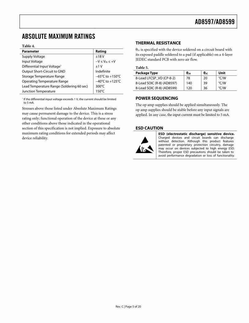
ABSOLUTE MAXIMUM RATINGS THERMAL RESISTANCE
Table 4. Parameter Rating Supply Voltage ±18 V Input Voltage −V ≤ VIN ≤ +V
Differential Input Voltage1 ±1 V Output Short-Circuit to GND Indefinite Storage Temperature Range −65°C to +150°C Operating Temperature Range −40°C to +125°C Lead Temperature Range (Soldering 60 sec) 300°C Junction Temperature 150°C
θJA is specified with the device soldered on a circuit board with its exposed paddle soldered to a pad (if applicable) on a 4-layer JEDEC standard PCB with zero air flow.
Table 5. Package Type θJA θJC Unit 8-Lead LFCSP_VD (CP-8-2) 78 20 °C/W 8-Lead SOIC (R-8) (AD8597) 140 39 °C/W 8-Lead SOIC (R-8) (AD8599) 120 36 °C/W
POWER SEQUENCING 1 If the differential input voltage exceeds 1 V, the current should be limited to 5 mA. The op amp supplies should be applied simultaneously. The
op amp supplies should be stable before any input signals are applied. In any case, the input current must be limited to 5 mA.
Stresses above those listed under Absolute Maximum Ratings may cause permanent damage to the device. This is a stress rating only; functional operation of the device at these or any other conditions above those indicated in the operational section of this specification is not implied. Exposure to absolute maximum rating conditions for extended periods may affect device reliability.
ESD CAUTION
AD8597/AD8599
Rev. C | Page 6 of 20
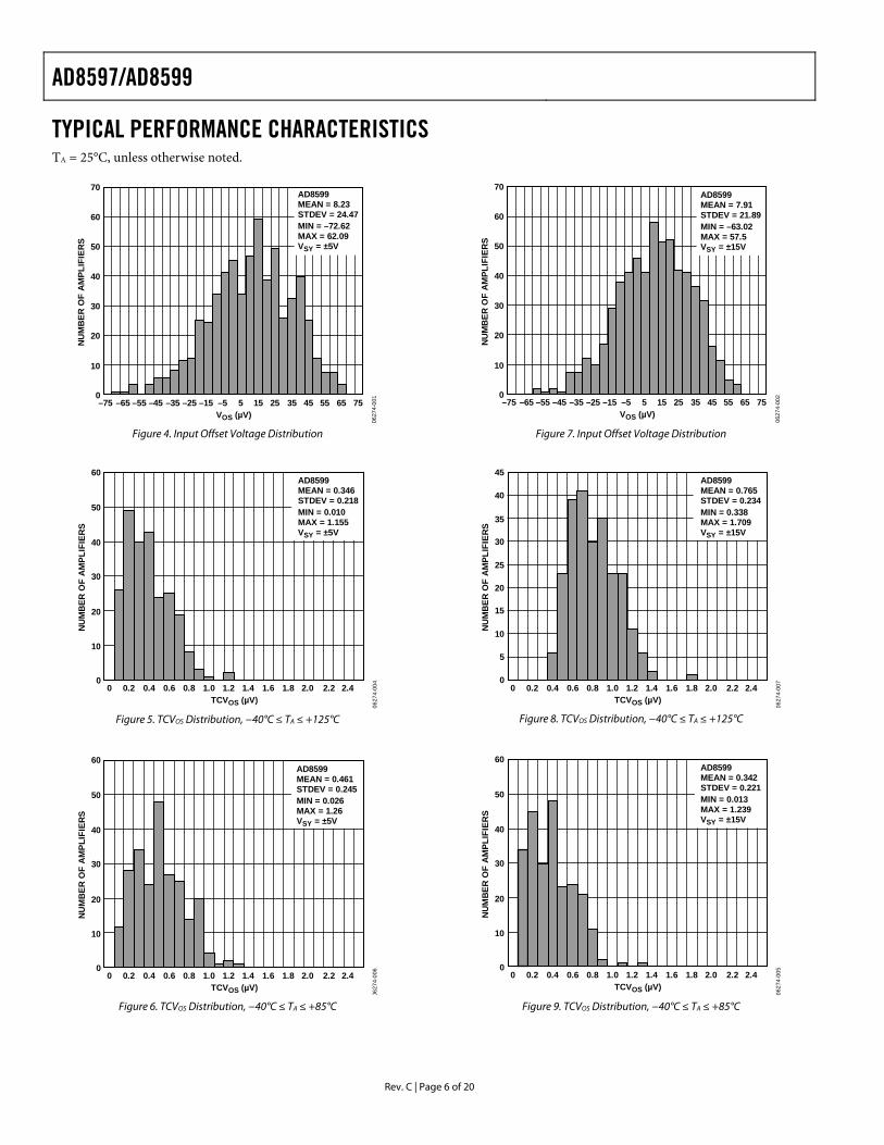
TYPICAL PERFORMANCE CHARACTERISTICS TA = 25°C, unless otherwise noted.
–75 –65 –55 –45 –35 –25 –15 –5 15 25 35 45 55 65 755
70
60
50
40
30
20
10
0
NU
MB
ER O
F A
MPL
IFIE
RS
VOS (µV)
AD8599MEAN = 8.23STDEV = 24.47MIN = –72.62MAX = 62.09VSY = ±5V
0627
4-00
1
Figure 4. Input Offset Voltage Distribution
0 0.2 1.6 1.8 2.0 2.41.41.21.00.4 0.6 0.8 2.2
60
50
40
30
20
10
0
NU
MB
ER O
F A
MPL
IFIE
RS
TCVOS (µV)
AD8599MEAN = 0.346STDEV = 0.218MIN = 0.010MAX = 1.155VSY = ±5V
0627
4-00
4
Figure 5. TCVOS Distribution, −40°C ≤ TA ≤ +125°C
0 0.2 1.6 1.8 2.0 2.41.41.21.00.4 0.6 0.8 2.2
60
50
40
30
20
10
0
NU
MB
ER O
F A
MPL
IFIE
RS
TCVOS (µV)
AD8599MEAN = 0.461STDEV = 0.245MIN = 0.026MAX = 1.26VSY = ±5V
0627
4-00
6
Figure 6. TCVOS Distribution, −40°C ≤ TA ≤ +85°C
–75 –65 –55 –45 –35 –25 –15 –5 15 25 35 45 55 65 755
70
60
50
40
30
20
10
0
NU
MB
ER O
F A
MPL
IFIE
RS
VOS (µV)
AD8599MEAN = 7.91STDEV = 21.89MIN = –63.02MAX = 57.5VSY = ±15V
0627
4-00
2
Figure 7. Input Offset Voltage Distribution
0 0.2 1.6 1.8 2.0 2.41.41.21.00.4 0.6 0.8 2.2
45
40
35
30
25
20
15
NU
MB
ER O
F A
MPL
IFIE
RS
TCVOS (µV)
10
5
0
AD8599MEAN = 0.765STDEV = 0.234MIN = 0.338MAX = 1.709VSY = ±15V
0627
4-00
7
Figure 8. TCVOS Distribution, −40°C ≤ TA ≤ +125°C
0 0.2 1.6 1.8 2.0 2.41.41.21.00.4 0.6 0.8 2.2
60
50
40
30
20
10
0
NU
MB
ER O
F A
MPL
IFIE
RS
TCVOS (µV)
AD8599MEAN = 0.342STDEV = 0.221MIN = 0.013MAX = 1.239VSY = ±15V
0627
4-00
5
Figure 9. TCVOS Distribution, −40°C ≤ TA ≤ +85°C
AD8597/AD8599
Rev. C | Page 7 of 20
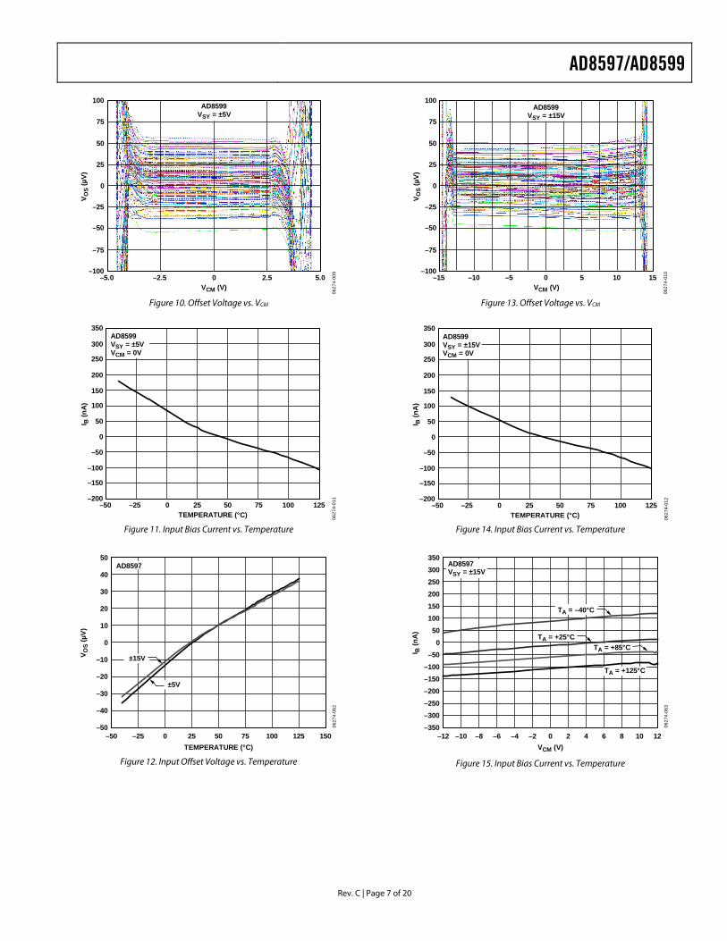
–5.0 –2.5 0 2.5 5.0
100
75
50
25
0
–25
–100
V OS
(µV)
VCM (V)
–50
–75
0627
4-00
9
AD8599VSY = ±5V
Figure 10. Offset Voltage vs. VCM
–50 –25 0 25 50
350
300
250
200
150
100
–200
I B (n
A)
TEMPERATURE (°C)
50
0
75 100
–50
–100
–150
125
0627
4-01
1AD8599VSY = ±5VVCM = 0V
Figure 11. Input Bias Current vs. Temperature
50
40
30
20
10
0
–10
–20
–30
–40
–50–50 –25 0 25 50 75 100 125 150
V OS
(µV)
TEMPERATURE (°C)
0627
4-06
2
AD8597
±15V
±5V
Figure 12. Input Offset Voltage vs. Temperature
–15 –10 –5 0 5
100
75
50
25
0
–25
–100
V OS
(µV)
VCM (V)
–50
–75
10 15
0627
4-01
0
AD8599VSY = ±15V
Figure 13. Offset Voltage vs. VCM
–50 –25 0 25 50
350
300
250
200
150
100
–200
I B (n
A)
TEMPERATURE (°C)
50
0
75 100
–50
–100
–150
125
0627
4-01
2
AD8599VSY = ±15VVCM = 0V
Figure 14. Input Bias Current vs. Temperature
350
–300–250–200–150–100
–500
50100150200250300
–350–12 –10 –8 –6 –4 –2 0 2 4 6 8 10 12
I B (n
A)
VCM (V)
0627
4-06
3
AD8597VSY = ±15V
TA = –40°C
TA = +25°C
TA = +125°C
TA = +85°C
Figure 15. Input Bias Current vs. Temperature
AD8597/AD8599
Rev. C | Page 8 of 20
–50 –25 0 25 50
80
70
60
50
40
30
I OS
(nA
)
TEMPERATURE (°C)
20
10
75 1000
125
IOS @ VSY = ±15V
IOS @ VSY = ±5V
0627
4-01
3
AD8599
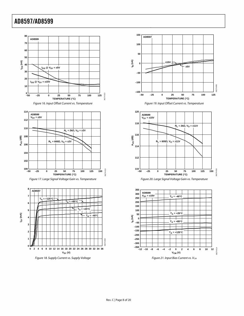
Figure 16. Input Offset Current vs. Temperature
150125–50 –25 0 25 50
114
112
110
108
106
104
AVO
(dB
)
TEMPERATURE (°C)
102
10075 100
RL = 2kΩ, VO = ±2V
RL = 600Ω, VO = ±2V
0627
4-01
5
AD8599VSY = ±5V
Figure 17. Large Signal Voltage Gain vs. Temperature
8
7
6
5
4
3
2
1
00 2 4 6 8 10 12 14 16 18 20 22 24 26 28 30 32 34 36
I SY
(mA
)
VSY (V)
0627
4-06
4
AD8597
TA = +25°C
TA = –40°C
TA = +85°CTA = +125°C
Figure 18. Supply Current vs. Supply Voltage
150
100
50
0
–50
–100
–150–50 –25 0 25 50 75 100 125
I B (n
A)
TEMPERATURE (°C)
0627
4-06
5
AD8597
±15V
±5V
Figure 19. Input Offset Current vs. Temperature
150125–50 –25 0 25 50
120
118
116
114
112
110
AVO
(dB
)
TEMPERATURE (°C)75 100
RL = 2kΩ, VO = ±11V
RL = 600Ω, VO = ±11V
0627
4-01
6
AD8599VSY = ±15V
Figure 20. Large Signal Voltage Gain vs. Temperature
42–12 –10 –8 –6 –4
350
300250200150
100
I B (n
A)
VCM (V)
50
0
–2 0–350
6
–50–100–150
–200–250
–300
108 12
TA = +25°C
TA = –40°C
TA = +85°C
TA = +125°C
0627
4-01
4
AD8599VSY = ±15V
Figure 21. Input Bias Current vs. VCM
AD8597/AD8599
Rev. C | Page 9 of 20
150125–50 –25 0 25 50
80
60
40
20
0
–80
OU
TPU
T C
UR
REN
T (m
A)
TEMPERATURE (°C)75 100
ISINK
–20
–40
–60
ISOURCE
0627
4-01
7
AD8599VSY = ±5V
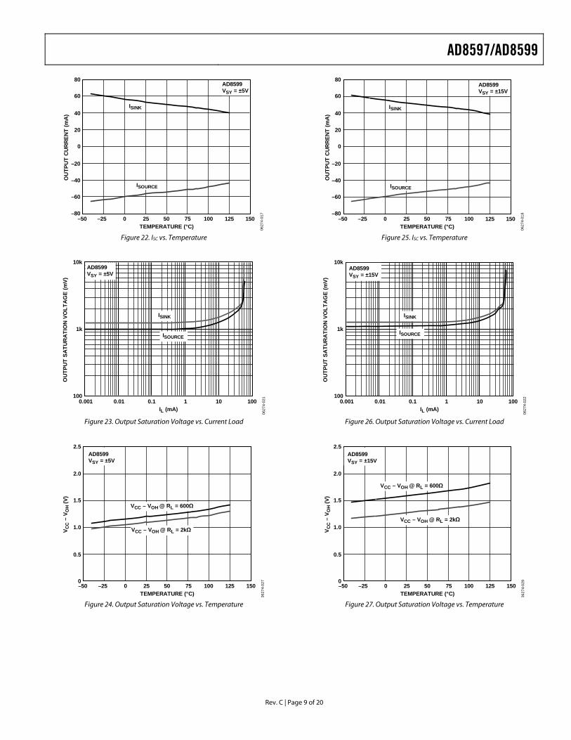
Figure 22. ISC vs. Temperature
0.001 0.01 0.1 1 10
10k
1k
100
OU
TPU
T SA
TUR
ATI
ON
VO
LTA
GE
(mV)
IL (mA)100
ISOURCE
ISINK
0627
4-02
1AD8599VSY = ±5V
Figure 23. Output Saturation Voltage vs. Current Load
–50 –25 0 25 50
2.5
2.0
1.5
1.0
0.5
0
V CC
– V
OH
(V)
TEMPERATURE (°C)75 100 125 150
VCC – VOH @ RL = 600Ω
VCC – VOH @ RL = 2kΩ
0627
4-02
7
AD8599VSY = ±5V
Figure 24. Output Saturation Voltage vs. Temperature
ISINK
150125–50 –25 0 25 50
80
60
40
20
0
–80
OU
TPU
T C
UR
REN
T (m
A)
TEMPERATURE (°C)75 100
–20
–40
–60
ISOURCE
0627
4-01
8
AD8599VSY = ±15V
Figure 25. ISC vs. Temperature
0.001 0.01 0.1 1 10
10k
1k
100
OU
TPU
T SA
TUR
ATI
ON
VO
LTA
GE
(mV)
IL (mA)100
ISOURCE
ISINK
0627
4-02
2
AD8599VSY = ±15V
Figure 26. Output Saturation Voltage vs. Current Load
–50 –25 0 25 50
2.5
2.0
1.5
1.0
0.5
0
V CC
– V
OH
(V)
TEMPERATURE (°C)75 100 125 150
VCC – VOH @ RL = 600Ω
VCC – VOH @ RL = 2kΩ06
274-
029
AD8599VSY = ±15V
Figure 27. Output Saturation Voltage vs. Temperature
AD8597/AD8599
Rev. C | Page 10 of 20
–50 –25 0 25 50
0
–0.5
–1.0
–1.5
–2.0
–2.5
V EE
– V O
L (V
)
TEMPERATURE (°C)75 100 125 150
VEE – VOL @ RL = 600Ω
VEE – VOL @ RL = 2kΩ
0627
4-02
8
AD8599VSY = ±5V
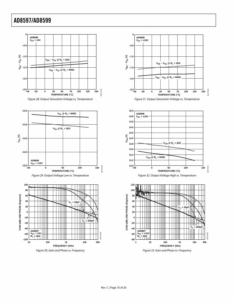
Figure 28. Output Saturation Voltage vs. Temperature
–50 0 50
–13.0
–13.5
V OL
(V)
TEMPERATURE (°C)100 150
VOL @ RL = 600Ω
VOL @ RL = 2kΩ
–14.0
–14.5
–15.0
0627
4-03
2
AD8599VSY = ±15V
Figure 29. Output Voltage Low vs. Temperature
100
–60
–40
–20
0
20
40
60
80
–100
–80
10 100 1k 10k 50kFREQUENCY (kHz)
0627
4-06
6
GA
IN (d
B) A
ND
PH
ASE
(Deg
rees
)
AD8597VSY = ±5VRL = 2kΩ
CL = 200pF
CL = 20pF
Figure 30. Gain and Phase vs. Frequency
–50 –25 0 25 50
0
–0.5
–1.0
–1.5
–2.0
–2.5
V EE
– V O
L (V
)
TEMPERATURE (°C)75 100 125 150
VEE – VOL @ RL = 600Ω
VEE – VOL @ RL = 2kΩ
0627
4-03
0
AD8599VSY = ±15V
Figure 31. Output Saturation Voltage vs. Temperature
–50 0 50
15.0
14.8
14.6
14.4
14.2
13.0
V OH
(V)
TEMPERATURE (°C)100 150
VOH @ RL = 600Ω
14.0
13.8
13.6
13.4
13.2
VOH @ RL = 2kΩ
0627
4-03
1
AD8599VSY = ±15V
Figure 32. Output Voltage High vs. Temperature
120
–40
–20
0
20
40
60
80
100
–80
–60
1 10 100 1k 50k10kFREQUENCY (kHz)
0627
4-06
7
GA
IN (d
B) A
ND
PH
ASE
(Deg
rees
)
AD8597VSY = ±15VRL = 2kΩ
CL = 200pF
CL = 20pF
Figure 33. Gain and Phase vs. Frequency
AD8597/AD8599
Rev. C | Page 11 of 20
1 10 100 1k 50k10k
50
–30
–20
–10
0
10
20
30
40
–40
GA
IN (d
B)
FREQUENCY (kHz)
0627
4-06
8
AD8597
AV = 1
AV = 10
AV = 100
VSY = ±5VRL = 2kΩ
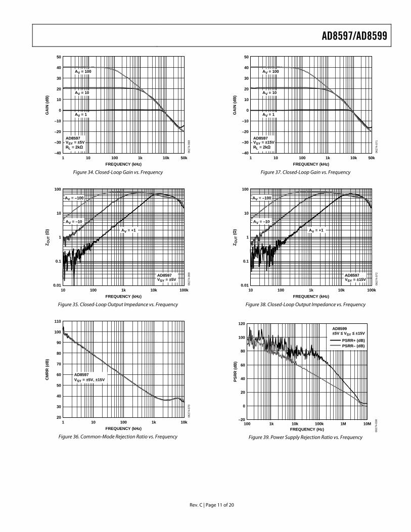
Figure 34. Closed-Loop Gain vs. Frequency
100
0.1
1
10
0.0110 100 1k 10k 100k
Z OU
T (Ω
)
FREQUENCY (kHz)
0627
4-06
9AD8597VSY = ±5V
AV = –100
AV = –10
AV = +1
Figure 35. Closed-Loop Output Impedance vs. Frequency
110
30
60
90
40
70
100
50
80
201 10 100 1k 10k
CM
RR
(dB
)
FREQUENCY (kHz)
0627
4-07
0
AD8597VSY = ±5V, ±15V
Figure 36. Common-Mode Rejection Ratio vs. Frequency
1 10 100 1k 50k10k
50
–30
–20
–10
0
10
20
30
40
–40
GA
IN (d
B)
FREQUENCY (kHz)
0627
4-07
1
AD8597
AV = 1
AV = 10
AV = 100
VSY = ±15VRL = 2kΩ
Figure 37. Closed-Loop Gain vs. Frequency
100
0.1
1
10
0.0110 100 1k 10k 100k
Z OU
T (Ω
)
FREQUENCY (kHz)
0627
4-07
2AD8597VSY = ±15V
AV = –100
AV = –10
AV = +1
Figure 38. Closed-Loop Output Impedance vs. Frequency
100 1k 10k 100k 1M
120
100
80
PSR
R (d
B)
FREQUENCY (Hz)10M
60
40
20
0
–20
PSRR+ (dB)PSRR– (dB)
0627
4-03
8
AD8599±5V ≤ VSY ≤ ±15V
Figure 39. Power Supply Rejection Ratio vs. Frequency
AD8597/AD8599
Rev. C | Page 12 of 20
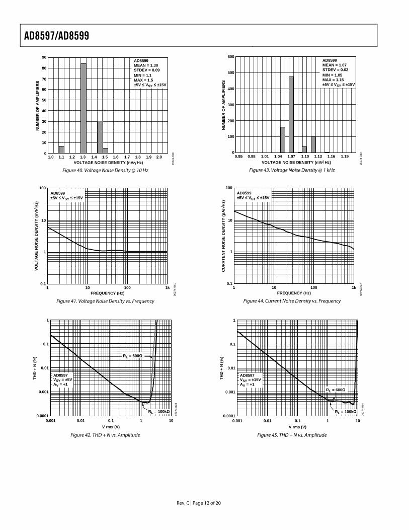
1.0 1.1 1.2 1.3 1.4 1.5 1.6 1.7 1.9 2.01.8
90
80
70
60
50
40
30
0
NU
MB
ER O
F A
MPL
IFIE
RS
VOLTAGE NOISE DENSITY (nV/ Hz)
20
10
AD8599MEAN = 1.30STDEV = 0.09MIN = 1.1MAX = 1.5±5V ≤ VSY ≤ ±15V
0627
4-03
9Figure 40. Voltage Noise Density @ 10 Hz
1 10 100 1k
100
1
0.1
FREQUENCY (Hz)
10
VOLT
AG
E N
OIS
E D
ENSI
TY (n
V/ H
z)
0627
4-04
1
AD8599±5V ≤ VSY ≤ ±15V
Figure 41. Voltage Noise Density vs. Frequency
1
0.001
0.01
0.1
0.00010.001 0.01 0.1 1 10
THD
+ N
(%)
V rms (V)
0627
4-07
3
AD8597VSY = ±5VAV = +1
RL = 600Ω
RL = 100kΩ
Figure 42. THD + N vs. Amplitude
0.95 0.98 1.01 1.04 1.07 1.10 1.13 1.16 1.19
600
500
400
300
200
100
0
NU
MB
ER O
F A
MPL
IFIE
RS
VOLTAGE NOISE DENSITY (nV/ Hz)
AD8599MEAN = 1.07STDEV = 0.02MIN = 1.05MAX = 1.15±5V ≤ VSY ≤ ±15V
0627
4-04
0
Figure 43. Voltage Noise Density @ 1 kHz
1 10 100
100
1
0.1
FREQUENCY (Hz)1k
10C
UR
RTE
NT
NO
ISE
DEN
SITY
(pA
/ H
z)
0627
4-04
2
AD8599±5V ≤ VSY ≤ ±15V
Figure 44. Current Noise Density vs. Frequency
1
0.001
0.01
0.1
0.00010.001 0.01 0.1 1 10
THD
+ N
(%)
V rms (V)
0627
4-07
4
AD8597VSY = ±15VAV = +1
RL = 600Ω
RL = 100kΩ
Figure 45. THD + N vs. Amplitude
AD8597/AD8599
Rev. C | Page 13 of 20
10 100 1k 10k 100k
0.1
0.01
0.001
THD
+ N
(%)
FREQUENCY (Hz)
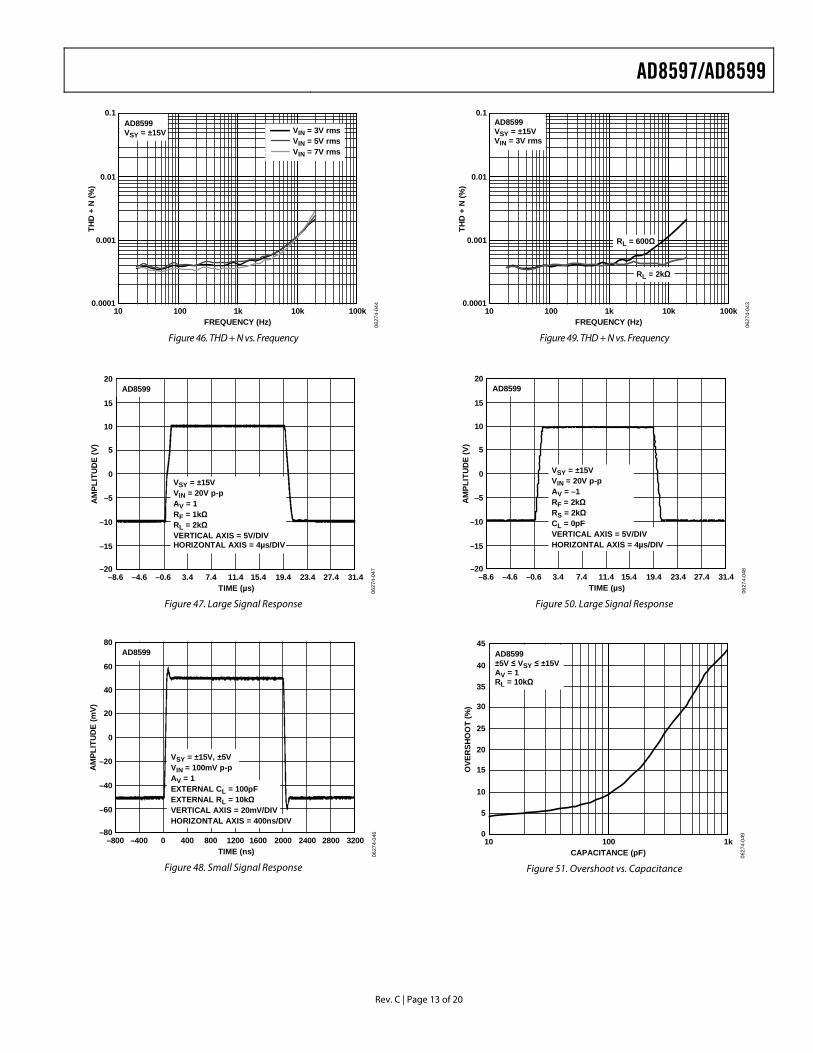
0.0001
VIN = 3V rmsVIN = 5V rmsVIN = 7V rms
0627
4-04
4
AD8599VSY = ±15V
Figure 46. THD + N vs. Frequency
–8.6 –4.6 –0.6 3.4 7.4 11.4 15.4 19.4 23.4
20
10
5
0
–5
–10
–15
AM
PLIT
UD
E (V
)
TIME (µs)
–20
15
27.4 31.4
VSY = ±15VVIN = 20V p-pAV = 1RF = 1kΩRL = 2kΩVERTICAL AXIS = 5V/DIVHORIZONTAL AXIS = 4µs/DIV
0627
4-04
7
AD8599
Figure 47. Large Signal Response
–800 –400 0 400 800 1200 1600 2000 2400
80
40
20
0
–20
–40
–60
AM
PLIT
UD
E (m
V)
TIME (ns)
–80
60
2800 3200
VSY = ±15V, ±5VVIN = 100mV p-pAV = 1EXTERNAL CL = 100pFEXTERNAL RL = 10kΩVERTICAL AXIS = 20mV/DIVHORIZONTAL AXIS = 400ns/DIV
0627
4-04
6
AD8599
Figure 48. Small Signal Response
10 100 1k 10k 100k
0.1
0.01
0.001
THD
+ N
(%)
FREQUENCY (Hz)
0.0001
RL = 600Ω
RL = 2kΩ
0627
4-04
3
AD8599VSY = ±15VVIN = 3V rms
Figure 49. THD + N vs. Frequency
–8.6 –4.6 –0.6 3.4 7.4 11.4 15.4 19.4 23.4
20
10
5
0
–5
–10
–15
AM
PLIT
UD
E (V
)
TIME (µs)
–20
15
27.4 31.4
VSY = ±15VVIN = 20V p-pAV = –1RF = 2kΩRS = 2kΩCL = 0pFVERTICAL AXIS = 5V/DIVHORIZONTAL AXIS = 4µs/DIV
0627
4-04
8
AD8599
Figure 50. Large Signal Response
10 100 1k
45
40
35
OVE
RSH
OO
T (%
)
CAPACITANCE (pF)
30
25
20
15
10
5
0
0627
4-04
9
AD8599±5V ≤ VSY ≤ ±15VAV = 1RL = 10kΩ
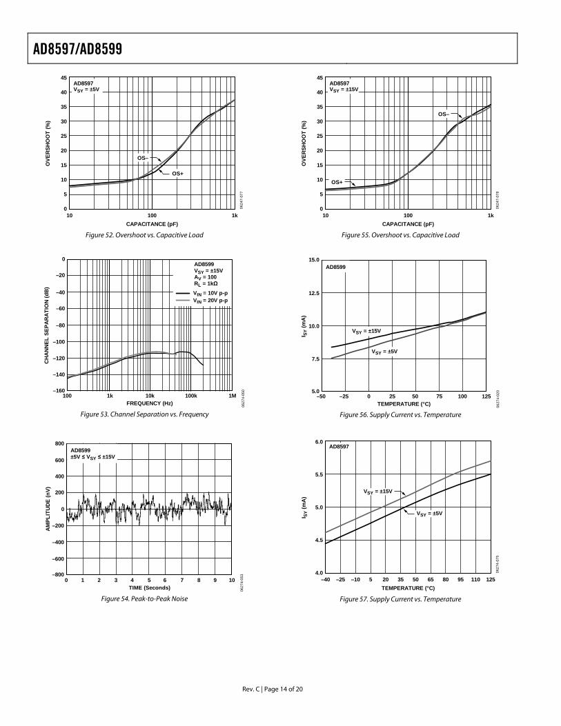
Figure 51. Overshoot vs. Capacitance
AD8597/AD8599
Rev. C | Page 14 of 20
45
40
35
30
25
20
15
10
5
010 100 1k
OVE
RSH
OO
T (%
)
CAPACITANCE (pF)
0624
7-07
7
OS–
AD8597VSY = ±5V
OS+
Figure 52. Overshoot vs. Capacitive Load
100 1k 10k 100k 1M
0
–20
–120CH
AN
NEL
SEP
AR
ATI
ON
(dB
)
FREQUENCY (Hz)
–40
–60
–80
–100
–160
–140
VIN = 10V p-pVIN = 20V p-p
0627
4-05
0
AD8599VSY = ±15VAV = 100RL = 1kΩ
Figure 53. Channel Separation vs. Frequency
0 1 2 3 4 5 6 7 8
800
400
200
0
–200
–400
–600
AM
PLIT
UD
E (n
V)
TIME (Seconds)
–800
600
9 10
0627
4-05
3
AD8599±5V ≤ VSY ≤ ±15V
Figure 54. Peak-to-Peak Noise
45
40
35
30
25
20
15
10
5
010 100 1k
OVE
RSH
OO
T (%
)
CAPACITANCE (pF)
0624
7-07
8
OS–
AD8597VSY = ±15V
OS+
Figure 55. Overshoot vs. Capacitive Load
125–50 –25 0 25 50
15.0
12.5
10.0
7.5
5.0
I SY
(mA
)
TEMPERATURE (°C)75 100
VSY = ±15V
0627
4-02
0
AD8599
VSY = ±5V
Figure 56. Supply Current vs. Temperature
6.0
4.5
5.0
5.5
4.0–40 –25 –10 5 20 35 50 65 80 95 110 125
I SY
(mA
)
TEMPERATURE (°C)
0627
4-07
5
AD8597
VSY = ±15V
VSY = ±5V
Figure 57. Supply Current vs. Temperature
AD8597/AD8599
Rev. C | Page 15 of 20
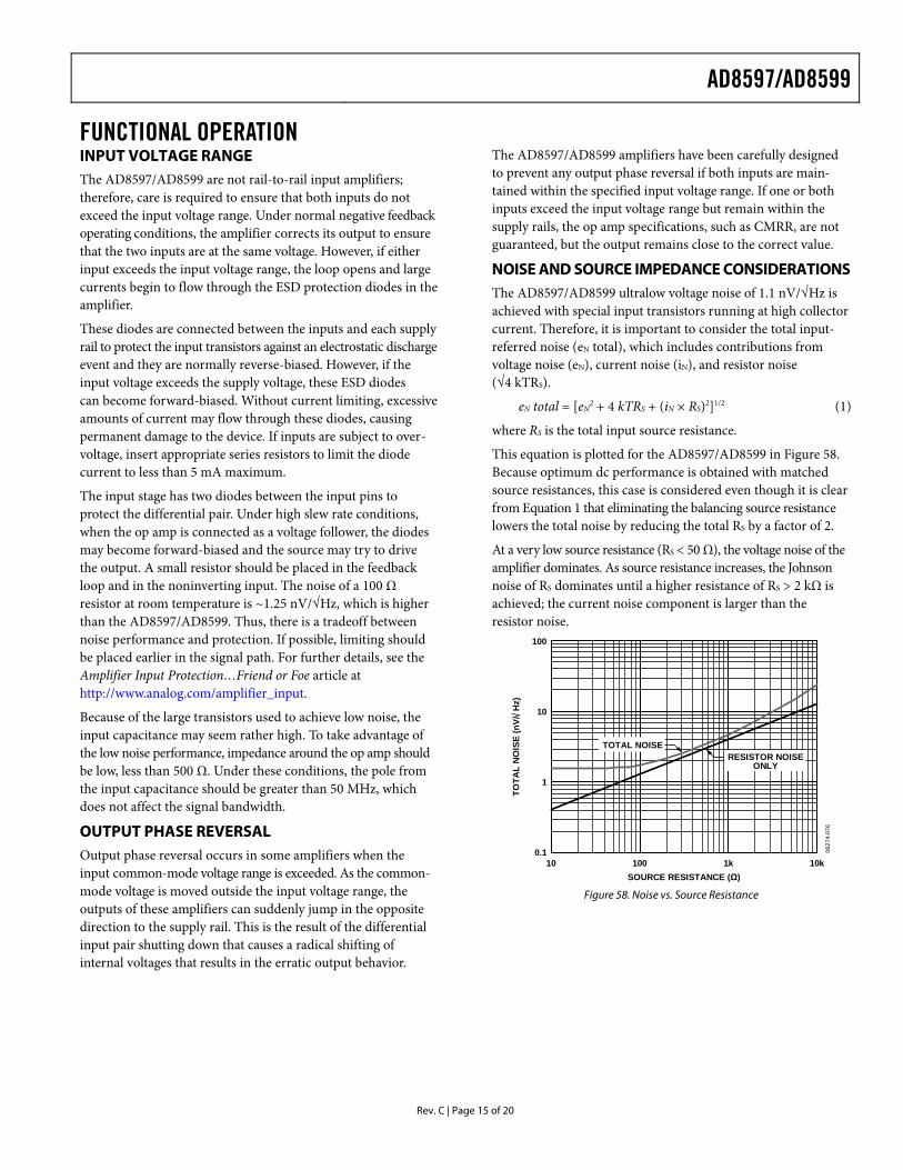
FUNCTIONAL OPERATION INPUT VOLTAGE RANGE The AD8597/AD8599 are not rail-to-rail input amplifiers; therefore, care is required to ensure that both inputs do not exceed the input voltage range. Under normal negative feedback operating conditions, the amplifier corrects its output to ensure that the two inputs are at the same voltage. However, if either input exceeds the input voltage range, the loop opens and large currents begin to flow through the ESD protection diodes in the amplifier.
These diodes are connected between the inputs and each supply rail to protect the input transistors against an electrostatic discharge event and they are normally reverse-biased. However, if the input voltage exceeds the supply voltage, these ESD diodes can become forward-biased. Without current limiting, excessive amounts of current may flow through these diodes, causing permanent damage to the device. If inputs are subject to over-voltage, insert appropriate series resistors to limit the diode current to less than 5 mA maximum.
The input stage has two diodes between the input pins to protect the differential pair. Under high slew rate conditions, when the op amp is connected as a voltage follower, the diodes may become forward-biased and the source may try to drive the output. A small resistor should be placed in the feedback loop and in the noninverting input. The noise of a 100 Ω resistor at room temperature is ~1.25 nV/√Hz, which is higher than the AD8597/AD8599. Thus, there is a tradeoff between noise performance and protection. If possible, limiting should be placed earlier in the signal path. For further details, see the Amplifier Input Protection…Friend or Foe article at http://www.analog.com/amplifier_input.
Because of the large transistors used to achieve low noise, the input capacitance may seem rather high. To take advantage of the low noise performance, impedance around the op amp should be low, less than 500 Ω. Under these conditions, the pole from the input capacitance should be greater than 50 MHz, which does not affect the signal bandwidth.
OUTPUT PHASE REVERSAL Output phase reversal occurs in some amplifiers when the input common-mode voltage range is exceeded. As the common-mode voltage is moved outside the input voltage range, the outputs of these amplifiers can suddenly jump in the opposite direction to the supply rail. This is the result of the differential input pair shutting down that causes a radical shifting of internal voltages that results in the erratic output behavior.
The AD8597/AD8599 amplifiers have been carefully designed to prevent any output phase reversal if both inputs are main-tained within the specified input voltage range. If one or both inputs exceed the input voltage range but remain within the supply rails, the op amp specifications, such as CMRR, are not guaranteed, but the output remains close to the correct value.
NOISE AND SOURCE IMPEDANCE CONSIDERATIONS The AD8597/AD8599 ultralow voltage noise of 1.1 nV/√Hz is achieved with special input transistors running at high collector current. Therefore, it is important to consider the total input-referred noise (eN total), which includes contributions from voltage noise (eN), current noise (iN), and resistor noise (√4 kTRS).
eN total = [eN2 + 4 kTRS + (iN × RS)2]1/2 (1)
where RS is the total input source resistance.
This equation is plotted for the AD8597/AD8599 in Figure 58. Because optimum dc performance is obtained with matched source resistances, this case is considered even though it is clear from Equation 1 that eliminating the balancing source resistance lowers the total noise by reducing the total RS by a factor of 2.
At a very low source resistance (RS < 50 Ω), the voltage noise of the amplifier dominates. As source resistance increases, the Johnson noise of RS dominates until a higher resistance of RS > 2 kΩ is achieved; the current noise component is larger than the resistor noise.
100
1
10
0.110 100 1k 10k
TOTA
L N
OIS
E (n
V/ H
z)
SOURCE RESISTANCE (Ω)
0627
4-07
6
TOTAL NOISERESISTOR NOISE
ONLY
Figure 58. Noise vs. Source Resistance
AD8597/AD8599
Rev. C | Page 16 of 20
The AD8597/AD8599 are the optimum choice for low noise performance if the source resistance is kept < 1 kΩ. At higher values of source resistance, optimum performance with respect to only noise is obtained with other amplifiers from Analog Devices. Both voltage noise and current noise need to be consi-dered. For more information on avoiding noise from grounding problems and inadequate bypassing, see the AN-345 Application Note, Grounding for Low- and High-Frequency Circuits. For
general noise theory with extensive calculations, see the AN-358 Application Note, Noise and Operational Amplifier Circuits. A good selection table for low noise op amps can be found in AN-940 Application Note, Low Noise Amplifier Selection Guide for Optimal Noise Performance. An interesting note on using one section of a monolithic dual to phase compen-sate the other section is in the AN-107 Application Note, Active Feedback Improves Amplifier Phase Accuracy.
0624
7-07
9
+
–
V+
V–
VBC1
Q36
Q32
R1
R31
R32
D2D31
D34OUTPUT
D3
6INVERTING
INPUT
7
2
3
4
NONINVERTINGINPUT
D1R18 R19
D2
D41
Q18 Q19
Q19
Q27
Q20
Q28
D42
D39
D40
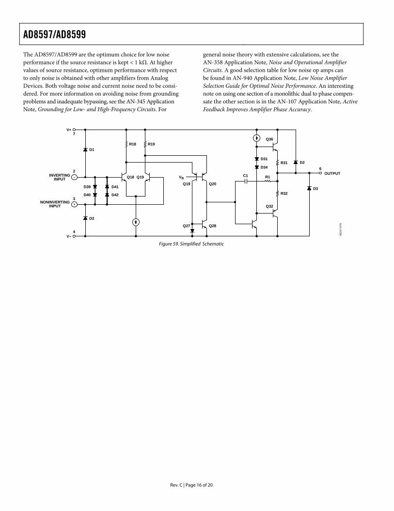
Figure 59. Simplified Schematic
AD8597/AD8599
Rev. C | Page 17 of 20
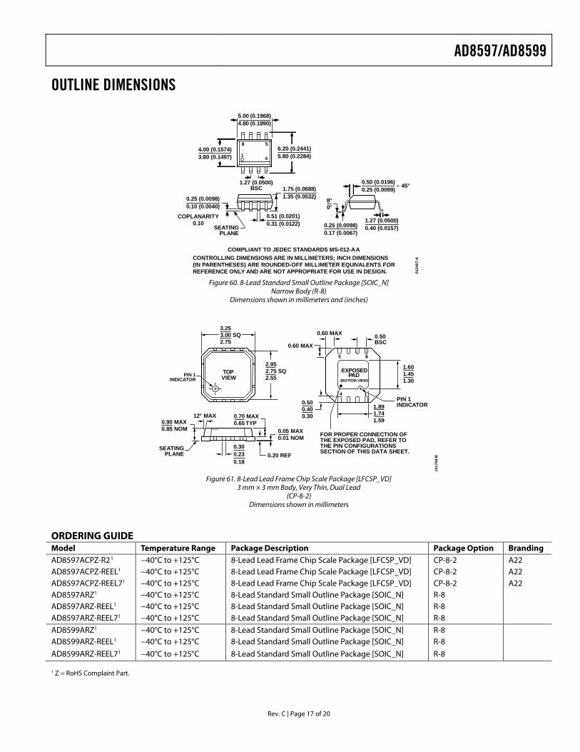
OUTLINE DIMENSIONS
CONTROLLING DIMENSIONS ARE IN MILLIMETERS; INCH DIMENSIONS(IN PARENTHESES) ARE ROUNDED-OFF MILLIMETER EQUIVALENTS FORREFERENCE ONLY AND ARE NOT APPROPRIATE FOR USE IN DESIGN.
COMPLIANT TO JEDEC STANDARDS MS-012-AA
0124
07-A
0.25 (0.0098)0.17 (0.0067)
1.27 (0.0500)0.40 (0.0157)
0.50 (0.0196)0.25 (0.0099)
45°
8°0°
1.75 (0.0688)1.35 (0.0532)
SEATINGPLANE
0.25 (0.0098)0.10 (0.0040)
41
8 5
5.00 (0.1968)4.80 (0.1890)
4.00 (0.1574)3.80 (0.1497)
1.27 (0.0500)BSC
6.20 (0.2441)5.80 (0.2284)
0.51 (0.0201)0.31 (0.0122)
COPLANARITY0.10
Figure 60. 8-Lead Standard Small Outline Package [SOIC_N]
Narrow Body (R-8) Dimensions shown in millimeters and (inches)
1017
08-B
1
EXPOSEDPAD
(BOTTOM VIEW)
0.50BSC
PIN 1INDICATOR0.50
0.400.30
TOPVIEW
12° MAX 0.70 MAX0.65 TYP0.90 MAX
0.85 NOM 0.05 MAX0.01 NOM
0.20 REF
1.891.741.59
4
1.601.451.30
3.253.00 SQ2.75
2.952.75 SQ2.55
5 8
PIN 1INDICATOR
SEATINGPLANE
0.300.230.18
0.60 MAX
0.60 MAX
FOR PROPER CONNECTION OFTHE EXPOSED PAD, REFER TOTHE PIN CONFIGURATIONSSECTION OF THIS DATA SHEET.
Figure 61. 8-Lead Lead Frame Chip Scale Package [LFCSP_VD]
3 mm × 3 mm Body, Very Thin, Dual Lead (CP-8-2)
Dimensions shown in millimeters
ORDERING GUIDE Model Temperature Range Package Description Package Option Branding AD8597ACPZ-R21 −40°C to +125°C 8-Lead Lead Frame Chip Scale Package [LFCSP_VD] CP-8-2 A22 AD8597ACPZ-REEL1 −40°C to +125°C 8-Lead Lead Frame Chip Scale Package [LFCSP_VD] CP-8-2 A22 AD8597ACPZ-REEL71 −40°C to +125°C 8-Lead Lead Frame Chip Scale Package [LFCSP_VD] CP-8-2 A22 AD8597ARZ1 −40°C to +125°C 8-Lead Standard Small Outline Package [SOIC_N] R-8 AD8597ARZ-REEL1 −40°C to +125°C 8-Lead Standard Small Outline Package [SOIC_N] R-8 AD8597ARZ-REEL71 −40°C to +125°C 8-Lead Standard Small Outline Package [SOIC_N] R-8 AD8599ARZ1 −40°C to +125°C 8-Lead Standard Small Outline Package [SOIC_N] R-8 AD8599ARZ-REEL1 −40°C to +125°C 8-Lead Standard Small Outline Package [SOIC_N] R-8
AD8599ARZ-REEL71 −40°C to +125°C 8-Lead Standard Small Outline Package [SOIC_N] R-8 1 Z = RoHS Complaint Part.

AD8597/AD8599
Rev. C | Page 18 of 20
NOTES

AD8597/AD8599
Rev. C | Page 19 of 20
NOTES
AD8597/AD8599
Rev. C | Page 20 of 20
NOTES
©2007–2009 Analog Devices, Inc. All rights reserved. Trademarks and registered trademarks are the property of their respective owners. D06274-0-12/09(C)