Embed Size (px)
Citation preview
1 IntroductionThe FlexMemory (FlexNVM and FlexRAM) is available onFreescale’s MC56F84xxx family of digital signal controllers(DSC). The FlexMemory allows the user to configure theFlexNVM block as either basic data flash, enhanced EEPROM(EEE) flash, or a combination of both.
The EEPROM feature is widely used in applications that storesmall amount of rapidly changing data required to be savedunder system power off.
This application describes the features of FlexMemory andenhanced EEPROM (EEE), EEPROM user perspective,EEPROM system-on-chip implementation, write enduranceperformance, and design considerations. It also includes anexample project of EEPROM design on MC56F84789 deviceto show how to design EEPROM in a user application.
2 Features of FlexMemoryand enhanced EEPROM
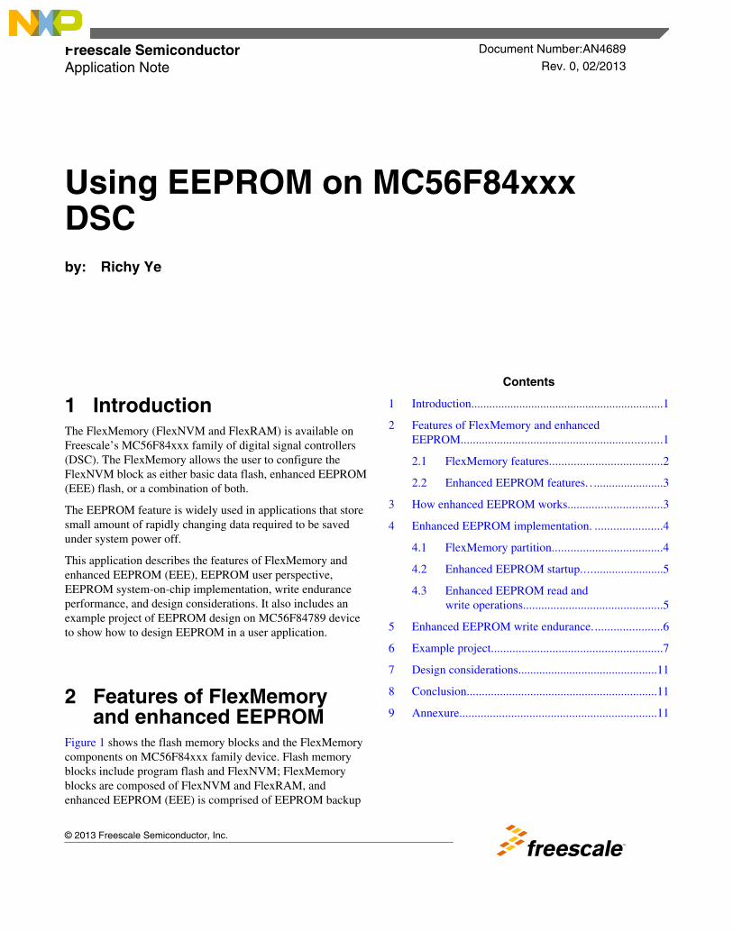
Figure 1 shows the flash memory blocks and the FlexMemorycomponents on MC56F84xxx family device. Flash memoryblocks include program flash and FlexNVM; FlexMemoryblocks are composed of FlexNVM and FlexRAM, andenhanced EEPROM (EEE) is comprised of EEPROM backup
Freescale Semiconductor Document Number:AN4689
Application Note Rev. 0, 02/2013
Using EEPROM on MC56F84xxxDSCby: Richy Ye
© 2013 Freescale Semiconductor, Inc.
Contents
1 Introduction................................................................1
2 Features of FlexMemory and enhancedEEPROM..................................................................1
2.1 FlexMemory features.....................................2
2.2 Enhanced EEPROM features. . .......................3
3 How enhanced EEPROM works...............................3
4 Enhanced EEPROM implementation. ......................4
4.1 FlexMemory partition....................................4
4.2 Enhanced EEPROM startup...........................5
4.3 Enhanced EEPROM read andwrite operations..............................................5
5 Enhanced EEPROM write endurance.......................6
6 Example project........................................................7
7 Design considerations..............................................11
8 Conclusion...............................................................11
9 Annexure.................................................................11
in FlexNVM, FlexRAM and EEE state machine. FlexNVM and FlexRAM are the only memories used for enhancedEEPROM implementation.
Figure 1. Block diagram of flash memory blocks and FlexMemory components
FlexMemory features
2.1.1 FlexNVM featuresFollowing are the features of FlexNVM, when it is partitioned for data flash memory.
• Sector size of 1 KB• Protection scheme prevents accidental programming or erasing of stored data.• Automated, built-in program and erase algorithms with verify• Section programming for faster bulk programming times• Read access to data flash memory is possible while programming or erasing data in the program flash memory.
2.1.2 FlexRAM features• Memory can be used as traditional RAM or high-endurance EEPROM.• Up to 2 KB of FlexRAM configured for traditional RAM or EEPROM operations.• When configured for EEPROM:
• Protection scheme prevents accidental programming or erasing of data written for EEPROM.• Built-in hardware emulation scheme to automate EEPROM record maintenance functions• Programmable EEPROM data set size and FlexNVM partition code facilitating EEPROM memory endurance
trade-offs
2.1
FlexMemory features
Using EEPROM on MC56F84xxx DSC, Rev. 0, 02/2013
2 Freescale Semiconductor, Inc.
• Supports FlexRAM aligned writes of 1, 2, or 4 bytes at a time• Read access to FlexRAM is possible while programming or erasing data in the program or data flash memory.
• When configured for traditional RAM:• Read and write access is possible to the FlexRAM while programming or erasing data in the program or data
flash memory.
2.2 Enhanced EEPROM featuresThe enhanced EEPROM (EEE) capability of the FlexMemory has a number of features that allow the replacement of externalEEPROMs and improves upon their performance.
Enhanced EEPROM features include:• Configurability to allow the designer to make trade-off decisions based on the EEE endurance requirement and the total
amount of EEE and data flash memory requirement• High-endurance EEE memory can reach over 100M cycles (depending on the configuration).• Supports byte, word, and long word access• Fast write operation time (about 175 µs for a word-write operation to a pre-erased space, and 385 µs for a word-write
operation)• EEE functionality across the full operating voltage range for the processor
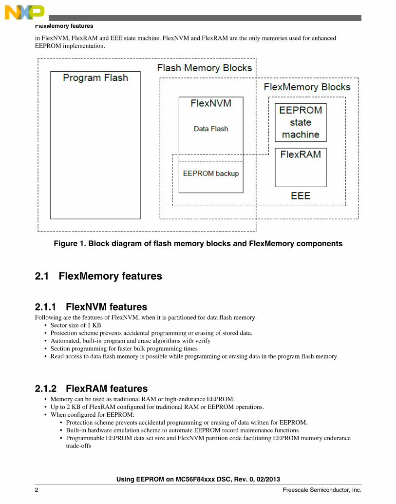
3 How enhanced EEPROM worksThe enhanced EEPROM system is shown in the following figure.
Figure 2. Top-level enhanced EEPROM architecture
To provide enhanced EEPROM (EEE) functionality, the FlexMemory uses a RAM block (FlexRAM), a flash block(FlexNVM), and EEE state machine. When the EEE functionality is enabled, the FlexRAM becomes EEE memory interface,which means that all of the EEE data is accessible at the FlexRAM address space. When the EEE is accessed, the EEE statemachine keeps track of the data and backs it up as data records, stored in some portion of the FlexNVM used as EEPROMbackup. Using a large partition of FlexNVM to back up the data for a small amount of EEE data allows the EEEimplementation to offer extremely high endurance.
The EEE state machine uses 32-bit records to back up data from the EEE into the flash. 16 bits of the record are used for thedata, and the other 16 bits are address and status information about the data. The data records are written and erased asneeded. This means that if a location within the EEPROM has never been accessed, there will not be a data record for it. Thishelps to reduce the amount of data that needs to be backed up and can increase the memory endurance.
How enhanced EEPROM works
Using EEPROM on MC56F84xxx DSC, Rev. 0, 02/2013
Freescale Semiconductor, Inc. 3
Enhanced EEPROM implementation
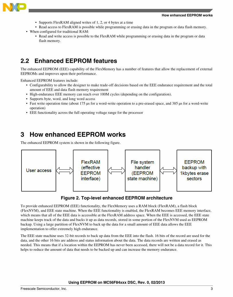
4.1 FlexMemory partitionTo use the EEE features, the memory has to be partitioned. The partitioning process tells the EEE state machine how muchEEE memory will be used and how much the FlexNVM will be used to back up the EEE.
Figure 3. FlexRAM to FlexNVM memory mapping
To handle varying customer requirements, the FlexRAM and FlexNVM blocks can be split into partitions as shown in Figure3. There are three programmable options that are used to define the exact memory use for a system. These parameters are:
• EEPROM partition (EEESIZE): The amount of FlexRAM used for EEPROM can be set from 0 bytes (no EEPROM)to the maximum FlexRAM size (2 KB). The remainder of the FlexRAM is not accessible while the FlexRAM isconfigured for EEPROM (use the Set FlexRAM Function command; see Set FlexRAM Function command in Chapter20 "Flash Memory Module" of MC56F847XXRM: MC56F847xx Reference Manual, available on freescale.com, formore information). The EEPROM partition grows upward from the bottom of the FlexRAM address space.
• Data flash partition (DEPART): The amount of FlexNVM memory used for data flash can be programmed from 0bytes (all of the FlexNVM block is available for EEPROM backup) to maximum size of the FlexNVM block (32 KB).
• FlexNVM EEPROM partition: The amount of FlexNVM memory used for EEPROM backup, which is equal to theFlexNVM block size minus the data flash memory partition size. The EEPROM backup size must be at least 16 timesthe EEPROM partition size in FlexRAM.
4
Enhanced EEPROM implementation
Using EEPROM on MC56F84xxx DSC, Rev. 0, 02/2013
4 Freescale Semiconductor, Inc.
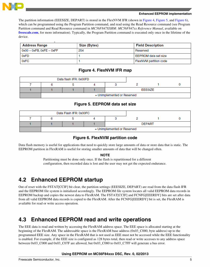
The partition information (EEESIZE, DEPART) is stored in the FlexNVM IFR (shown in Figure 4, Figure 5, and Figure 6),which can be programmed using the Program Partition command, and read using the Read Resource command (see ProgramPartition command and Read Resource command in MC56F847XXRM: MC56F847xx Reference Manual, available onfreescale.com, for more information). Typically, the Program Partition command is executed only once in the lifetime of thedevice.
Figure 4. FlexNVM IFR map
Figure 5. EEPROM data set size
Figure 6. FlexNVM partition code
Data flash memory is useful for applications that need to quickly store large amounts of data or store data that is static. TheEEPROM partition in FlexRAM is useful for storing smaller amounts of data that will be changed often.
NOTEPartitioning must be done only once. If the flash is repartitioned for a differentconfiguration, then recorded data is lost and the user may not get the expected endurance.
4.2 Enhanced EEPROM startupOut of reset with the FSTAT[CCIF] bit clear, the partition settings (EEESIZE, DEPART) are read from the data flash IFRand the EEPROM file system is initialized accordingly. The EEPROM file system locates all valid EEPROM data records inEEPROM backup and copies the newest data to FlexRAM. The FSTAT[CCIF] and FCNFG[EEERDY] bits are set after datafrom all valid EEPROM data records is copied to the FlexRAM. After the FCNFG[EEERDY] bit is set, the FlexRAM isavailable for read or write access operation.
4.3 Enhanced EEPROM read and write operationsThe EEE data is read and written by accessing the FlexRAM address space. The EEE space is allocated starting at thebeginning of the FlexRAM. The addressable space is the FlexRAM base address (0x03_C000, byte address) up to theprogrammed EEE size. Any space in the FlexRAM that is not used as EEE must not be accessed while the EEE functionalityis enabled. For example, if the EEE size is configured as 128 bytes total, then read or write accesses to any address spacebetween 0x03_C000 and 0x03_C07F are allowed, but 0x03_C080 to 0x03_C7FF will generate a bus error.
Enhanced EEPROM implementation
Using EEPROM on MC56F84xxx DSC, Rev. 0, 02/2013
Freescale Semiconductor, Inc. 5
Because the EEE data is accessed through a RAM, the data is readable and writable at any size, byte, word, or long word.Although any access size is possible, the records used to back up the EEE data use a word sized data field. This means thatbyte writes are possible, but it makes less efficient use of the EEPROM backup. That is why the endurance Equation 1 onpage 6 uses a different efficiency factor for 8-bit access than for 16-bit or 32-bit access.
4.3.1 Enhanced EEPROM write operationWhen configured for enhanced EEPROM use, write to the unprotected valid space in FlexRAM launches an EEE operationto store the data within the EEPROM backup in a round-robin fashion. Because this is a flash program operation, thesoftware must test the FSTAT[CCIF] bit (or FCNFG[EEERDY] bit) to determine if any other flash operations are in progressbefore writing to the EEE space. Because multiple concurrent writes and read-while-write operations within the same flashmemory block are not allowed, accesses to the EEE or FlexNVM space are not allowed until the EEE write is complete.
NOTEThe p-flash memory is a completely separate logical block, therefore read/write operationto the p-flash can continue normally while an EEE write is in progress.
4.3.2 Enhanced EEPROM read operationWhen the EEE is read, the data is supplied by the FlexRAM, and so no flash operation is trigerred. However, EEE read is notallowed while an EEE write is in progress. The software must either test the FCNFG[EEERDY] bit before read operation orwait for FCNFG[EEERDY] after a write operation before allowing the software to continue. In many cases, it is mostefficient for software to test FCNFG[EEERDY] bit (or FSTAT[CCIF] bit) both before and after the write operation and blockother EEE operations until FCNFG[EEERDY] bit sets after the write operation. This way a special function is needed forEEE write, but an EEE read doesn’t require any special software. Another advantage to this approach is that no additionaldelay or flag checking is required if there are multiple EEE read operations without EEE write operations in between.
A special case for an EEE read that must be considered is the first access to the EEE after a chip reset event. For the first readof the EEE after reset, the FCNFG[EEERDY] bit may need to be tested to make sure that the EEE state machine hascompleted the initial load of data from the EEPROM backup to the FlexRAM. If the system startup time is long, thisguarantees that the initial data load has enough time to complete before the first EEE read, then a test of theFCNFG[EEERDY] bit before the first read may not be required. However, it is safer to explicitly test the FCNFG[EEERDY]bit before the first read access to the EEE space.
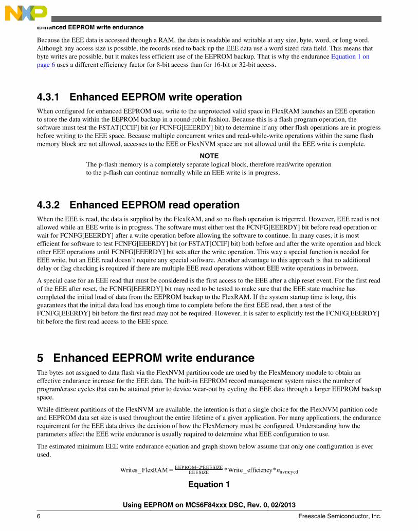
5 Enhanced EEPROM write enduranceThe bytes not assigned to data flash via the FlexNVM partition code are used by the FlexMemory module to obtain aneffective endurance increase for the EEE data. The built-in EEPROM record management system raises the number ofprogram/erase cycles that can be attained prior to device wear-out by cycling the EEE data through a larger EEPROM backupspace.
While different partitions of the FlexNVM are available, the intention is that a single choice for the FlexNVM partition codeand EEPROM data set size is used throughout the entire lifetime of a given application. For many applications, the endurancerequirement for the EEE data drives the decision of how the FlexMemory must be configured. Understanding how theparameters affect the EEE write endurance is usually required to determine what EEE configuration to use.
The estimated minimum EEE write endurance equation and graph shown below assume that only one configuration is everused.
Equation 1
Enhanced EEPROM write endurance
Using EEPROM on MC56F84xxx DSC, Rev. 0, 02/2013
6 Freescale Semiconductor, Inc.
Where:• Writes_ FlexRAM—minimum number of writes to each FlexRAM location• EEPROM—allocated FlexNVM for EEPROM backup based on DEPART of FlexNVM partition code in FlexNVM
IFR; programmed using the Program Partition command• EEESIZE—allocated FlexRAM for EEE data based on EEESIZE of EEPROM data set size in FlexNVM IFR;
programmed using the Program Partition command• Write_efficiency:
• 0.25 for 8-bit writes to FlexRAM• 0.5 for 16-bit or 32-bit writes to FlexRAM
• nnvmcycd—FlexNVM memory cycling endurance (the following figure assumes 10,000 cycles)
Figure 7. Enhanced EEPROM write endurance
Equation 1 on page 6 can be used to get a general idea of the amount of EEPROM backup memory that may be required forthe system. However, the equation is simplified and intended to be used as a general guideline.
6 Example projectThis example project discusses enhanced EEPROM operations on MC56F84xxx family DSC for user reference. To easilyand visually validate project operation result, a FreeMASTER project is also developed to directly observe the data changesin EEE space.
Example project
Using EEPROM on MC56F84xxx DSC, Rev. 0, 02/2013
Freescale Semiconductor, Inc. 7
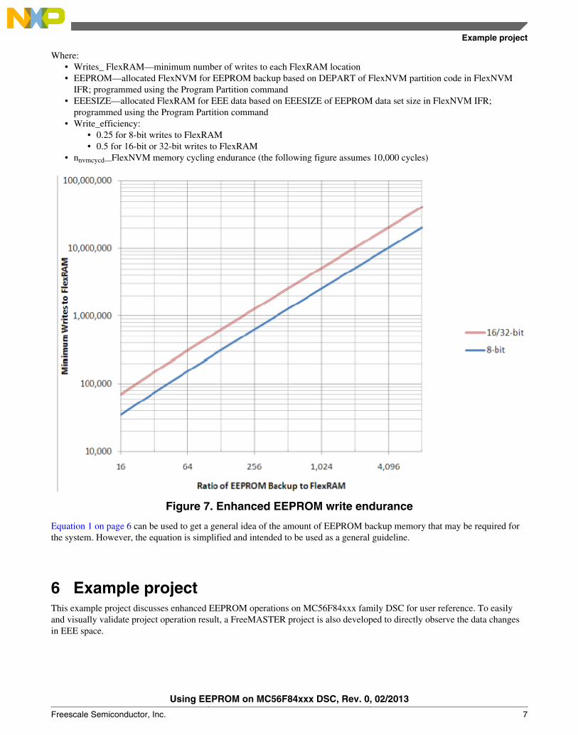
Figure 8 shows the code process flow in example project. The process blocks in light green are the key functional modulesfor EEE operations. And for EEPROM mass write process block, it completely complies with the description of EnhancedEEPROM write operation. The FCNFG[EEERDY] bit is tested before each EEE write operation to assure that no otherFlexNVM operation is in progress.
Besides, 8-bit, 16-bit, and 32-bit data written to EEE space are provided, and any type of write operation can be enabledthrough uncommenting the relevant code.
Figure 8. Flowchart of example project for EEE operations
The FreeMASTER project interface (open by Freescale free FreeMASTER application, which connects with target devicethrough USBTAP) is shown in Figure 9. All variables are listed in watch grid window, which are divided into three parts:
• The first part (in purple rectangle) lists the variable of EEPROM mass write enable flag. When this flag is set to 1, allvalid EEE space will be written by a predefined data array (source[SIZE_OF_BYTES])
• The secondary part (in red rectangle) lists the variables of on-chip memory configuration information, which helpverify the correctness of flash memory initialization function in code.
• The third part (in blue rectangle) lists all the variables in valid EEE space; this variable data is organized via a 256-bytedata array (eedata[SIZE_OF_BYTES]), which is assigned to valid EEE space (0x03C000 – 0x03C0FF, byte address) incode.
Example project
Using EEPROM on MC56F84xxx DSC, Rev. 0, 02/2013
8 Freescale Semiconductor, Inc.
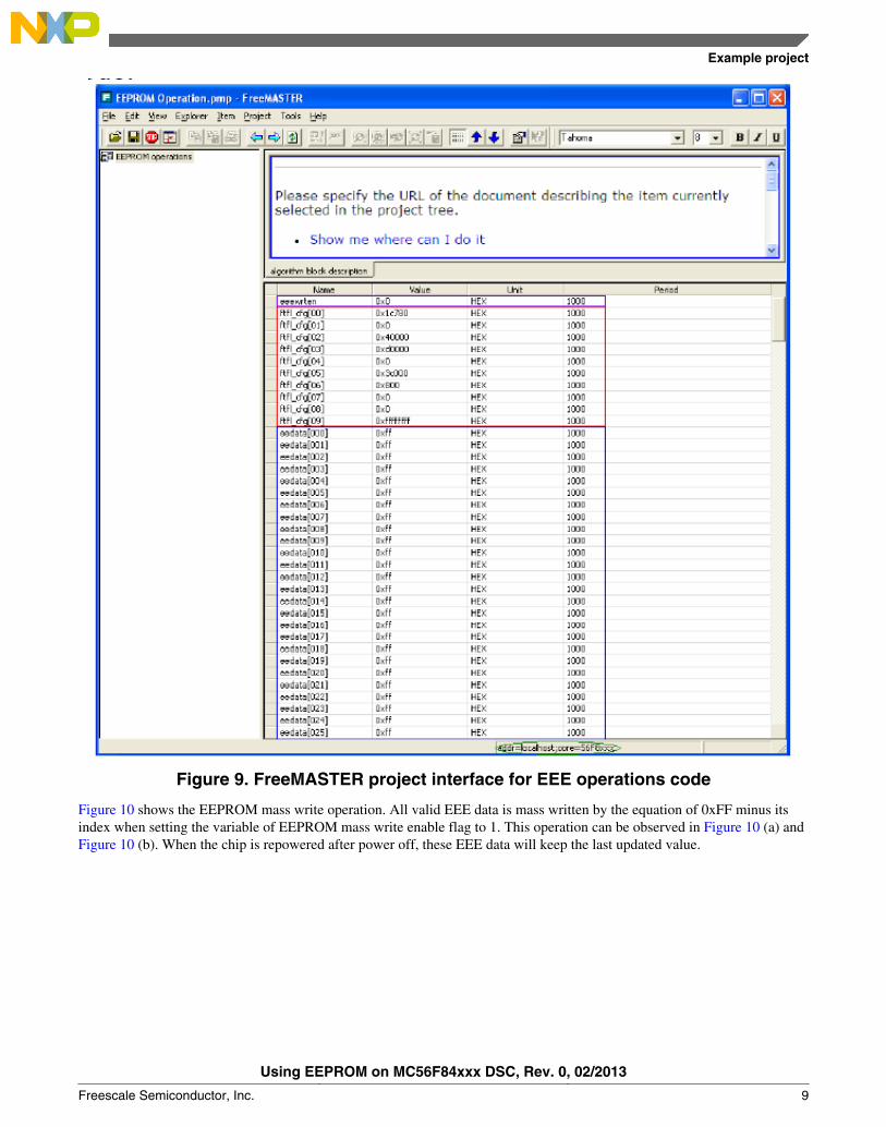
Figure 9. FreeMASTER project interface for EEE operations code
Figure 10 shows the EEPROM mass write operation. All valid EEE data is mass written by the equation of 0xFF minus itsindex when setting the variable of EEPROM mass write enable flag to 1. This operation can be observed in Figure 10 (a) andFigure 10 (b). When the chip is repowered after power off, these EEE data will keep the last updated value.
Example project
Using EEPROM on MC56F84xxx DSC, Rev. 0, 02/2013
Freescale Semiconductor, Inc. 9
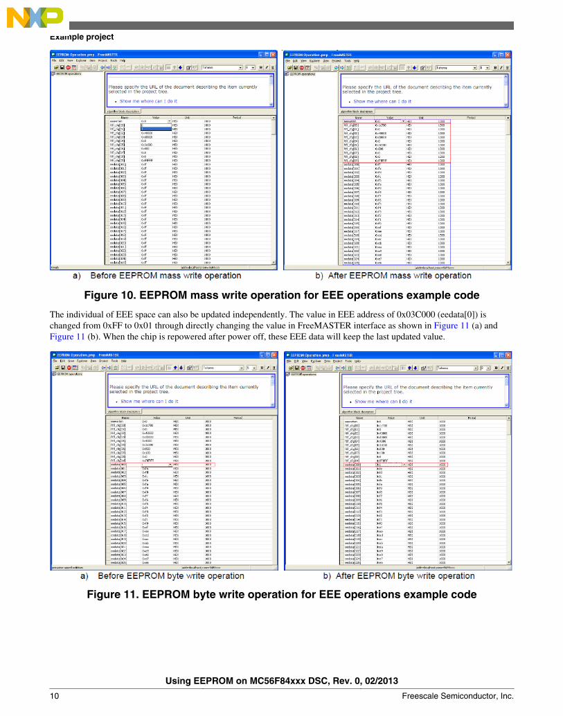
Figure 10. EEPROM mass write operation for EEE operations example code
The individual of EEE space can also be updated independently. The value in EEE address of 0x03C000 (eedata[0]) ischanged from 0xFF to 0x01 through directly changing the value in FreeMASTER interface as shown in Figure 11 (a) andFigure 11 (b). When the chip is repowered after power off, these EEE data will keep the last updated value.
Figure 11. EEPROM byte write operation for EEE operations example code
Example project
Using EEPROM on MC56F84xxx DSC, Rev. 0, 02/2013
10 Freescale Semiconductor, Inc.
7 Design considerationsAs known from Enhanced EEPROM features, the EEE write operation to a pre-erased space can help reduce the programtime because an erase cycle is not needed. This feature allows for quick data logging in time-critical situations. One typicalcase is that fault data and operating parameters need be stored when an imminent system power off is detected. The amountof data that needs to be saved times the maximum write time determines how much decoupling capacitors must be providedin this system to maintain minimum operating power long enough for the data to be stored. The significant decrease in theEEE program time by pre-erased data locations means that less decoupling capacitors is required and more data is stored inthis situation before power off.
The EEE state machine can detect if any EEE data has not been fully programmed. Any situation where EEE data is detectedas not fully programmed due to either a brownout or any reset during the write operation is treated the same. If a reset eventhappens while an EEE write is in progress, then the data can become corrupted. The EEE state machine tests vulnerable EEEdata record for values that may not be fully programmed. If an incomplete record is detected, the state machine marks thedata record as compromised and replaces it with the previous valid data record for the associated EEE address during the nextEEE write operation. This ensures that if an EEE write is interrupted for any reason, the user will get the last value that wasproperly written to the EEE space. Depending on how far into the write the reset occurred, this value can be either theprevious value or the new value, but the user will not get a corrupted value.
8 ConclusionThis application note summarizes the features, user perspective, SoC implementation and write endurance performance ofenhanced EEPROM function on MC56F84xxx DSC, and provides example code as attached (see AN4689SW.zip fileassociated with this application note) to help better understand functional implementation, and then make it easy for readersto use this feature in their applications. Finally, some design considerations are shared with readers for better use.
9 AnnexureThe example project is developed on MC56F84789 in CodeWarrior v10.3 IDE and the associated FreeMASTER project isalso attached in the package.
Design considerations
Using EEPROM on MC56F84xxx DSC, Rev. 0, 02/2013
Freescale Semiconductor, Inc. 11
How to Reach Us:
Home Page:www.freescale.com
Web Support:http://www.freescale.com/support
USA/Europe or Locations Not Listed:Freescale SemiconductorTechnical Information Center, EL5162100 East Elliot RoadTempe, Arizona 85284+1-800-521-6274 or +1-480-768-2130www.freescale.com/support
Europe, Middle East, and Africa:Freescale Halbleiter Deutschland GmbHTechnical Information CenterSchatzbogen 781829 Muenchen, Germany+44 1296 380 456 (English)+46 8 52200080 (English)+49 89 92103 559 (German)+33 1 69 35 48 48 (French)www.freescale.com/support
Japan:Freescale Semiconductor Japan Ltd.HeadquartersARCO Tower 15F1-8-1, Shimo-Meguro, Meguro-ku,Tokyo 153-0064Japan0120 191014 or +81 3 5437 [email protected]
Asia/Pacific:Freescale Semiconductor China Ltd.Exchange Building 23FNo. 118 Jianguo RoadChaoyang DistrictBeijing 100022China+86 10 5879 [email protected]
Document Number: AN4689Rev. 0, 02/2013
Information in this document is provided solely to enable system and softwareimplementers to use Freescale Semiconductors products. There are no express or impliedcopyright licenses granted hereunder to design or fabricate any integrated circuits orintegrated circuits based on the information in this document.
Freescale Semiconductor reserves the right to make changes without further notice to anyproducts herein. Freescale Semiconductor makes no warranty, representation, orguarantee regarding the suitability of its products for any particular purpose, nor doesFreescale Semiconductor assume any liability arising out of the application or use of anyproduct or circuit, and specifically disclaims any liability, including without limitationconsequential or incidental damages. "Typical" parameters that may be provided inFreescale Semiconductor data sheets and/or specifications can and do vary in differentapplications and actual performance may vary over time. All operating parameters,including "Typicals", must be validated for each customer application by customer'stechnical experts. Freescale Semiconductor does not convey any license under its patentrights nor the rights of others. Freescale Semiconductor products are not designed,intended, or authorized for use as components in systems intended for surgical implantinto the body, or other applications intended to support or sustain life, or for any otherapplication in which failure of the Freescale Semiconductor product could create asituation where personal injury or death may occur. Should Buyer purchase or useFreescale Semiconductor products for any such unintended or unauthorized application,Buyer shall indemnify Freescale Semiconductor and its officers, employees, subsidiaries,affiliates, and distributors harmless against all claims, costs, damages, and expenses, andreasonable attorney fees arising out of, directly or indirectly, any claim of personal injuryor death associated with such unintended or unauthorized use, even if such claims allegesthat Freescale Semiconductor was negligent regarding the design or manufacture ofthe part.
RoHS-compliant and/or Pb-free versions of Freescale products have the functionality andelectrical characteristics as their non-RoHS-complaint and/or non-Pb-free counterparts.For further information, see http://www.freescale.com or contact your Freescalesales representative.
For information on Freescale's Environmental Products program, go tohttp://www.freescale.com/epp.
Freescale™ and the Freescale logo are trademarks of Freescale Semiconductor, Inc.All other product or service names are the property of their respective owners.
© 2013 Freescale Semiconductor, Inc.


