Embed Size (px)
Citation preview
I N
V E
N T
I V
E
CONFIDENTIAL
Using GPUs to Speedup Computational Lithography
Constantin Chuyeshov
Bayram Yenikaya
GTC 2012
San Jose, CA
2
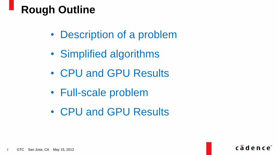
Rough Outline
GTC San Jose, CA May 15, 2012
• Description of a problem
• Simplified algorithms
• CPU and GPU Results
• Full-scale problem
• CPU and GPU Results
3
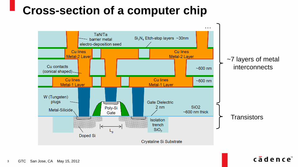
Cross-section of a computer chip
GTC San Jose, CA May 15, 2012
Transistors
~7 layers of metal
interconnects
…
4
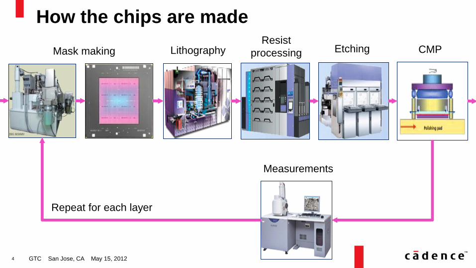
How the chips are made
GTC San Jose, CA May 15, 2012
Mask making Resist
processing Lithography Etching CMP
Measurements
Repeat for each layer
5
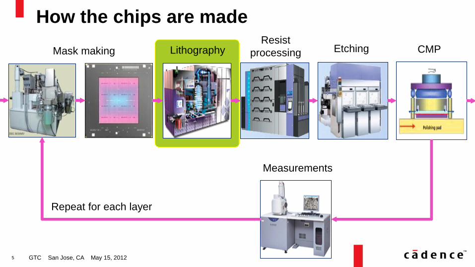
How the chips are made
GTC San Jose, CA May 15, 2012
Mask making Resist
processing Lithography Etching CMP
Measurements
Repeat for each layer
6
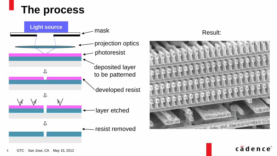
The process
GTC San Jose, CA May 15, 2012
photoresist
deposited layer
to be patterned
mask
projection optics
developed resist
layer etched
resist removed
Light source Result:
7
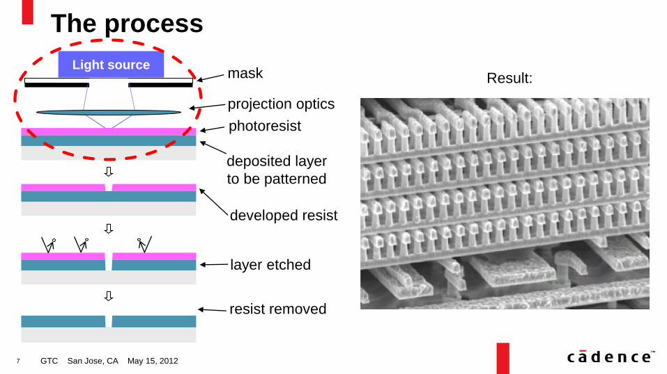
The process
GTC San Jose, CA May 15, 2012
photoresist
deposited layer
to be patterned
mask
projection optics
developed resist
layer etched
resist removed
Light source Result:
8
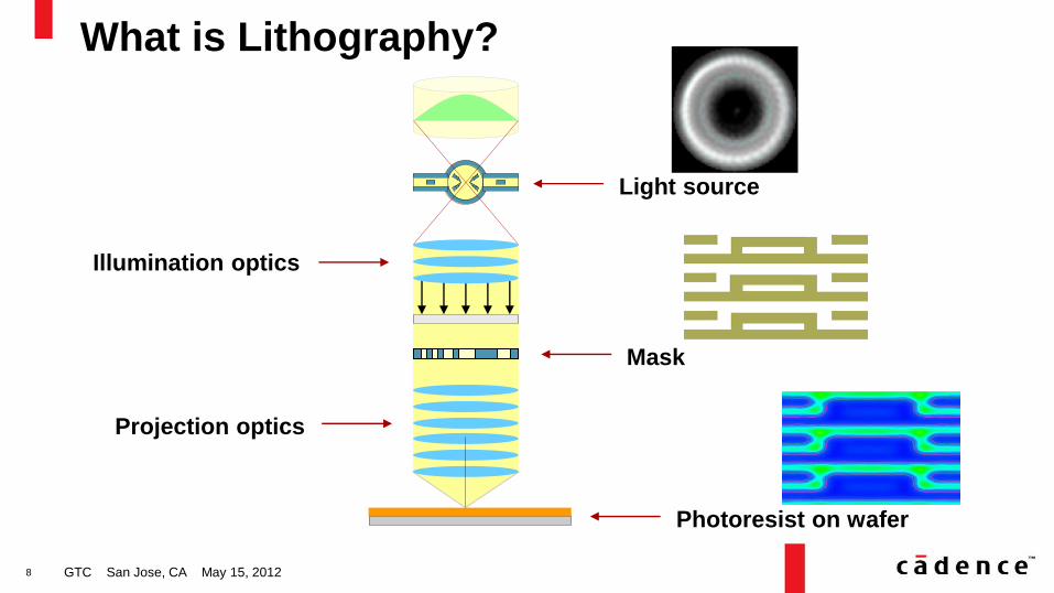
What is Lithography?
GTC San Jose, CA May 15, 2012
Light source
Illumination optics
Mask
Projection optics
Photoresist on wafer
9
Why Computational Lithography?
GTC San Jose, CA May 15, 2012
To print a satisfactory layer of a wafer you need to:
• Design and manufacture the mask
• Deposit various films on the wafer
• Expose the mask (optical lithography)
• Develop the resist
• Etch the unneeded areas
• Fill in the etched gaps with insulator
• Polish the surface
This might have to be done several times per layer to optimize the
mask design and to improve yield. It’s much cheaper and faster to
simulate it on a computer, than to manufacture.
10
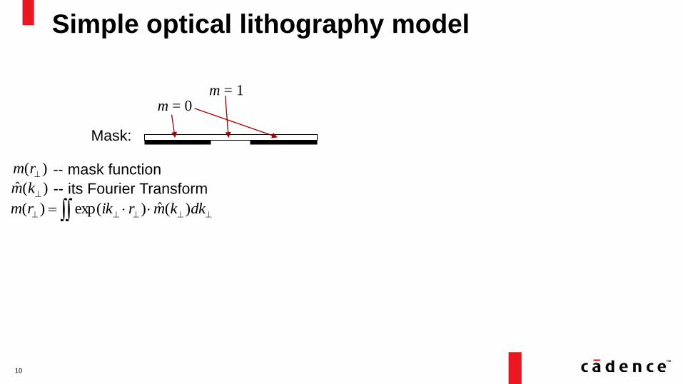
Simple optical lithography model
Mask:
m = 1 m = 0
-- mask function
dkkmrikrm )(ˆ)exp()(
)(ˆ km -- its Fourier Transform
)( rm
11
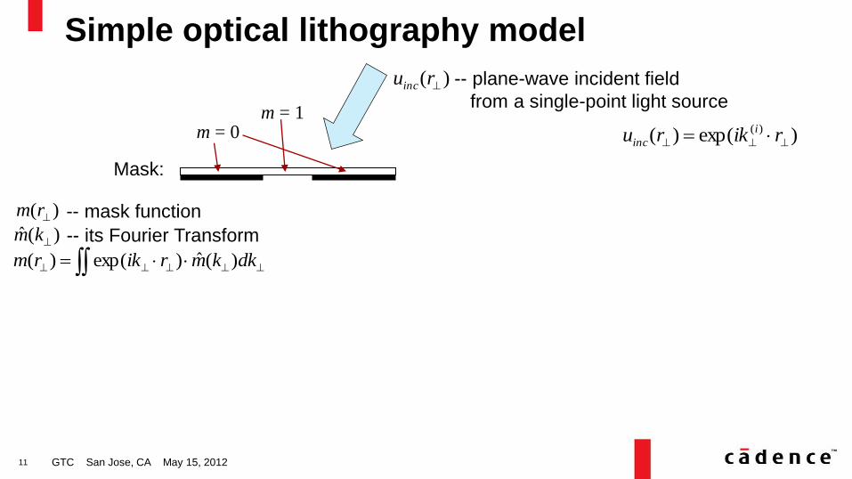
Simple optical lithography model
GTC San Jose, CA May 15, 2012
Mask:
m = 1 m = 0
-- mask function
dkkmrikrm )(ˆ)exp()(
)exp()( )(
rikru i
inc
)( ruinc -- plane-wave incident field
from a single-point light source
)(ˆ km -- its Fourier Transform
)( rm
12
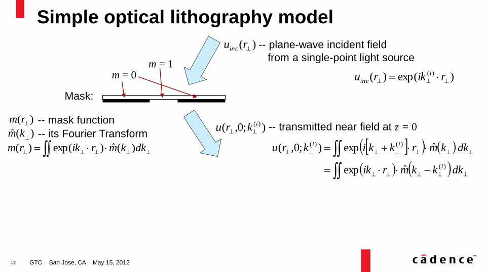
Simple optical lithography model
GTC San Jose, CA May 15, 2012
Mask:
m = 1 m = 0
-- mask function
dkkmrikrm )(ˆ)exp()(
)exp()( )(
rikru i
inc
)( ruinc -- plane-wave incident field
from a single-point light source
);0,( )(ikru -- transmitted near field at z = 0
dkkkmrik
dkkmrkkikru
i
ii
)(
)()(
ˆexp
ˆexp);0,(
)(ˆ km -- its Fourier Transform
)( rm
13
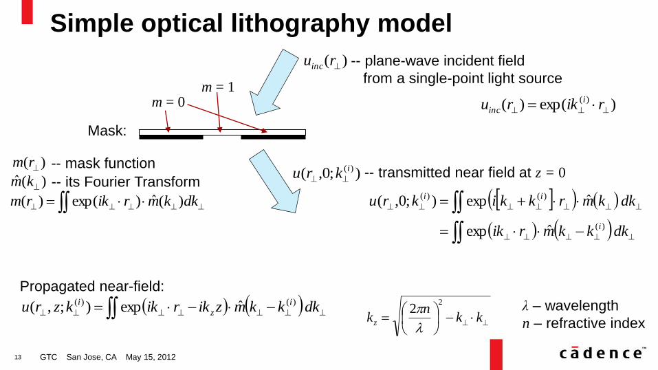
Simple optical lithography model
GTC San Jose, CA May 15, 2012
Mask:
m = 1 m = 0
-- mask function
dkkmrikrm )(ˆ)exp()(
)exp()( )(
rikru i
inc
)( ruinc -- plane-wave incident field
from a single-point light source
dkkkmzikrikkzru i
z
i )()( ˆexp);,(
);0,( )(ikru -- transmitted near field at z = 0
dkkkmrik
dkkmrkkikru
i
ii
)(
)()(
ˆexp
ˆexp);0,(
Propagated near-field:
)(ˆ km -- its Fourier Transform
)( rm
kk
nkz
22
λ – wavelength
n – refractive index
14
Simple optical lithography model
GTC San Jose, CA May 15, 2012
dkkkmkPzikrikkzru i
z
i )()( ˆ)(exp);,(
Including the lens aberrations and reflections ( ), the field becomes: )( kP
15
Simple optical lithography model
GTC San Jose, CA May 15, 2012
dkkkmkPzikrikkzru i
z
i )()( ˆ)(exp);,(
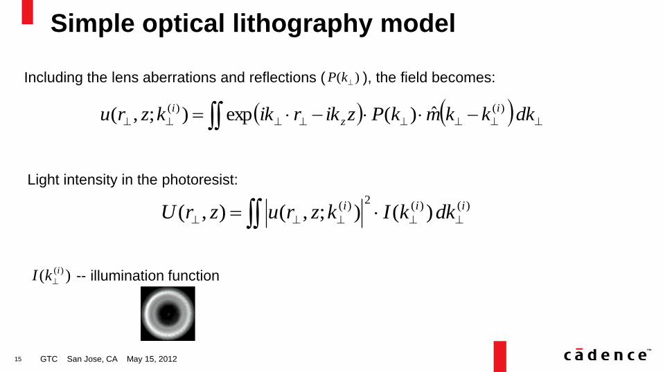
Including the lens aberrations and reflections ( ), the field becomes: )( kP
)()(2
)( )();,(),( iii dkkIkzruzrU
Light intensity in the photoresist:
)( )(ikI -- illumination function
16
Algorithm description
GTC San Jose, CA May 15, 2012
Given all the model parameters:
• Compute Fourier coefficients of the mask
• Compute light intensity at each point in the photoresist
17
Algorithm description
GTC San Jose, CA May 15, 2012
Given all the model parameters:
• Compute Fourier coefficients of the mask
• Compute light intensity at each point in the photoresist
However, there is a known physical limit on resolution of the optical system.
Thus, a faster algorithm:
• Compute Fourier coefficients of the mask
• Compute light intensity on coarse grid in the photoresist
• Interpolate the result to a dense grid
18
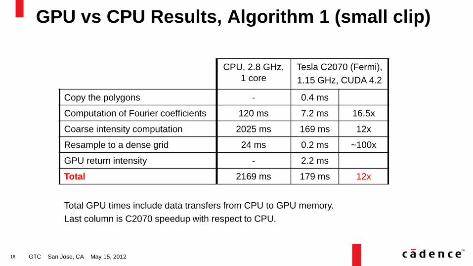
GPU vs CPU Results, Algorithm 1 (small clip)
GTC San Jose, CA May 15, 2012
CPU, 2.8 GHz,
1 core
Tesla C2070 (Fermi),
1.15 GHz, CUDA 4.2
Copy the polygons - 0.4 ms
Computation of Fourier coefficients 120 ms 7.2 ms 16.5x
Coarse intensity computation 2025 ms 169 ms 12x
Resample to a dense grid 24 ms 0.2 ms ~100x
GPU return intensity - 2.2 ms
Total 2169 ms 179 ms 12x
Total GPU times include data transfers from CPU to GPU memory.
Last column is C2070 speedup with respect to CPU.
19
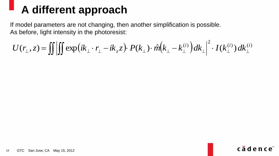
A different approach
GTC San Jose, CA May 15, 2012
If model parameters are not changing, then another simplification is possible.
As before, light intensity in the photoresist:
)()(2
)( )(ˆ)(exp),( iii
z dkkIdkkkmkPzikrikzrU
20
A different approach
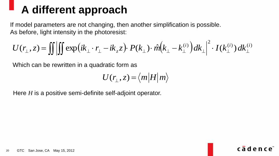
GTC San Jose, CA May 15, 2012
If model parameters are not changing, then another simplification is possible.
As before, light intensity in the photoresist:
)()(2
)( )(ˆ)(exp),( iii
z dkkIdkkkmkPzikrikzrU Which can be rewritten in a quadratic form as
mHmzrU ),(
Here H is a positive semi-definite self-adjoint operator.
21
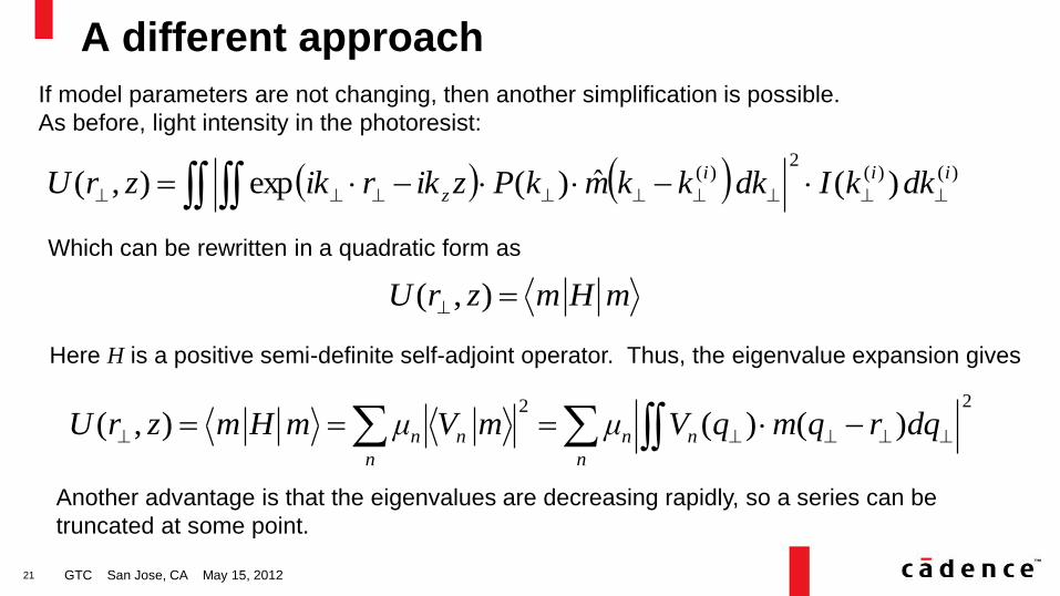
A different approach
GTC San Jose, CA May 15, 2012
If model parameters are not changing, then another simplification is possible.
As before, light intensity in the photoresist:
)()(2
)( )(ˆ)(exp),( iii
z dkkIdkkkmkPzikrikzrU Which can be rewritten in a quadratic form as
mHmzrU ),(
Here H is a positive semi-definite self-adjoint operator. Thus, the eigenvalue expansion gives
22
)()(),( dqrqmqVμmVμmHmzrU n
n
nn
n
n
Another advantage is that the eigenvalues are decreasing rapidly, so a series can be
truncated at some point.
22
Algorithm description
GTC San Jose, CA May 15, 2012
After precomputing the eigenvalues and eigenvectors:
• Compute Fourier coefficients of the mask
• Compute sum of squared convolutions to get light intensity on coarse
grid in the photoresist
• Interpolate the result to a dense grid
This approach is 5-15 times faster than the previous one, but loses the
flexibility to arbitrarily change the model during computation.

23
GPU vs CPU Results, Algorithm 2 (small clip)
GTC San Jose, CA May 15, 2012
CPU, 2.8 GHz,
1 core
Tesla C2070 (Fermi),
1.15 GHz, CUDA 4.2
Copy the polygons - 0.4 ms
Computation of Fourier coefficients 120 ms 7.2 ms 16.5x
Coarse intensity computation 55 ms 1.2 ms 46x
Resample to a dense grid 26 ms 0.2 ms ~100x
GPU return intensity - 2.2 ms
Total 201 ms 11.2 ms 18x
Total GPU times include data transfers from CPU to GPU memory.
Last column is C2070 speedup with respect to CPU.
24
Size of the problem
GTC San Jose, CA May 15, 2012
Suppose you want to simulate how a full computer chip of size L×L would
be printed on wafer.
• Fourier Coefficient computation ~ L4
• Intensity computation ~ L3 (approx.)
• Resampling ~ L2
Chip size (L) can be up to 10 mm, feature size can be down to 10 nm.
Each layer can be several 100’s Gb in size.
25
Size of the problem
GTC San Jose, CA May 15, 2012
Suppose you want to simulate how a full computer chip of size L×L would
be printed on wafer.
• Fourier Coefficient computation ~ L4
• Intensity computation ~ L3 (approx.)
• Resampling ~ L2
Chip size (L) can be up to 10 mm, feature size can be down to 10 nm.
Each layer can be several 100’s Gb in size.
Solution: break the chip into many small tiles, carefully choose the tile size,
deal with the boundary effects. Different tile sizes might be needed for CPU
and GPU.
26
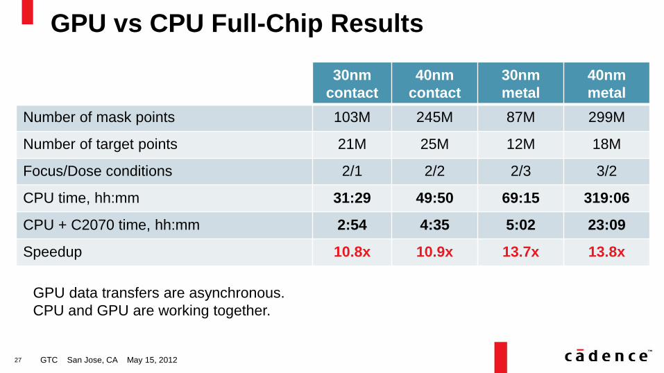
Full-Chip Results
GTC San Jose, CA May 15, 2012
• Full-chip verification
• Compute the intensity using second approach (model is not changing)
• Contour the intensity
• Check printability, critical dimensions, edge placement errors.
• 2 layers from 8.5mm × 8mm chip at 30nm node.
• 2 layers from 6.8mm × 7mm chip at 40nm node.
• Multiple focus and dose conditions.
1-core CPU at 2.8 GHz.
1-core CPU at 2.8 GHz and Tesla C2070 GPU at 1.15 GHz with CUDA 4.2.
27
GPU vs CPU Full-Chip Results
GTC San Jose, CA May 15, 2012
30nm
contact
40nm
contact
30nm
metal
40nm
metal
Number of mask points 103M 245M 87M 299M
Number of target points 21M 25M 12M 18M
Focus/Dose conditions 2/1 2/2 2/3 3/2
CPU time, hh:mm 31:29 49:50 69:15 319:06
CPU + C2070 time, hh:mm 2:54 4:35 5:02 23:09
Speedup 10.8x 10.9x 13.7x 13.8x
GPU data transfers are asynchronous.
CPU and GPU are working together.
28
Conclusions
GTC San Jose, CA May 15, 2012
• Before implementing anything on a GPU check if the CPU algorithm can
be improved (very often it can be!).
• CPU and GPU might have different optimal problem sizes.
In real-life applications, GPUs make speedups of 10-15x (with respect to 1
CPU) possible!


![2 LASER INTERFERENCE LITHOGRAPHY - uni-halle.de · 2 LASER INTERFERENCE LITHOGRAPHY (LIL) 9 2 LASER INTERFERENCE LITHOGRAPHY (LIL) Laser interference lithography [3~22] (LIL) is a](https://img.pdfslide.net/doc/110x75/5eae180eecc7e273a41a4e88/2-laser-interference-lithography-uni-hallede-2-laser-interference-lithography.jpg)