Embed Size (px)
Citation preview

Using Hardened Control Functions in MachXO3D Devices
Technical Note
FPGA-TN-02117-1.0
July 2021

Using Hardened Control Functions in MachXO3D Devices Technical Note
© 2021 Lattice Semiconductor Corp. All Lattice trademarks, registered trademarks, patents, and disclaimers are as listed at www.latticesemi.com/legal. All other brand or product names are trademarks or registered trademarks of their respective holders. The specifications and information herein are subject to change without notice.
2 FPGA-TN-02117-1.0
Disclaimers Lattice makes no warranty, representation, or guarantee regarding the accuracy of information contained in this document or the suitability of its products for any particular purpose. All information herein is provided AS IS and with all faults, and all risk associated with such information is entirely with Buyer. Buyer shall not rely on any data and performance specifications or parameters provided herein. Products sold by Lattice have been subject to limited testing and it is the Buyer's responsibility to independently determine the suitability of any products and to test and verify the same. No Lattice products should be used in conjunction with mission- or safety-critical or any other application in which the failure of Lattice’s product could create a situation where personal injury, death, severe property or environmental damage may occur. The information provided in this document is proprietary to Lattice Semiconductor, and Lattice reserves the right to make any changes to the information in this document or to any products at any time without notice.

Using Hardened Control Functions in MachXO3D Devices Technical Note
© 2021 Lattice Semiconductor Corp. All Lattice trademarks, registered trademarks, patents, and disclaimers are as listed at www.latticesemi.com/legal. All other brand or product names are trademarks or registered trademarks of their respective holders. The specifications and information herein are subject to change without notice.
FPGA-TN-02117-1.0 3
Contents Acronyms in This Document ................................................................................................................................................. 6 1. Introduction .................................................................................................................................................................. 7 2. WISHBONE Bus Interface .............................................................................................................................................. 9
2.1. WISHBONE Protocol .......................................................................................................................................... 10 2.2. WISHBONE Design Tips ..................................................................................................................................... 10
3. Generating an EFB Module with IPexpress ................................................................................................................. 11 4. Hardened I²C IP Cores ................................................................................................................................................. 15
4.1. Primary I²C ......................................................................................................................................................... 16 4.2. Secondary I2C .................................................................................................................................................... 18 4.3. Configuring I2C Cores with IPexpress ................................................................................................................ 19
4.3.1. General Call Enable ...................................................................................................................................... 19 4.3.2. Wake-up Enable ........................................................................................................................................... 20 4.3.3. I2C Bus Performance ..................................................................................................................................... 20 4.3.4. I2C Addressing ............................................................................................................................................... 20 4.3.5. MachXO3D I2C Usage Cases ......................................................................................................................... 20 4.3.6. I2C Design Tips .............................................................................................................................................. 22
5. Hardened SPI IP Core .................................................................................................................................................. 23 5.1. SPI Interface Signals .......................................................................................................................................... 24 5.2. Configuring the SPI Core with IPexpress ........................................................................................................... 26
5.2.1. SPI Mode ...................................................................................................................................................... 26 5.2.2. SPI Master Clock Rate ................................................................................................................................... 26 5.2.3. SPI Protocol Options ..................................................................................................................................... 27 5.2.4. Master Chip Selects ...................................................................................................................................... 27 5.2.5. SPI Controller Interrupts .............................................................................................................................. 27 5.2.6. Wake-up Enable ........................................................................................................................................... 28 5.2.7. MachXO3D SPI Usage Cases ......................................................................................................................... 28 5.2.8. SPI Design Tips .............................................................................................................................................. 30
6. Timer/Counter ............................................................................................................................................................ 31 6.1. Timer/Counter Modes of Operation ................................................................................................................. 32
6.1.1. Clear Timer on Compare Match Mode ......................................................................................................... 32 6.1.2. Watchdog Timer Mode ................................................................................................................................ 32 6.1.3. Fast PWM Mode ........................................................................................................................................... 33 6.1.4. Phase and Frequency Correct PWM Mode .................................................................................................. 33
6.2. Timer/Counter IP Signals ................................................................................................................................... 34 6.3. Configuring the Timer/Counter ......................................................................................................................... 34
6.3.1. Timer/Counter Mode ................................................................................................................................... 35 6.3.2. Output Function ........................................................................................................................................... 35 6.3.3. Clock Edge Selection ..................................................................................................................................... 35 6.3.4. Pre-scale Divider Value ................................................................................................................................. 36 6.3.5. Timer/Counter Top ....................................................................................................................................... 36 6.3.6. Output Compare Value ................................................................................................................................ 36 6.3.7. Enable Interrupt Registers ............................................................................................................................ 36 6.3.8. MachXO3D Timer/Counter Usage Cases ...................................................................................................... 36
6.3.8.1. Basic counter with interrupts ............................................................................................................... 36 6.3.8.2. Watchdog Timer ................................................................................................................................... 37 6.3.8.3. PWM Output with variable duty cycle and period ............................................................................... 37 6.3.8.4. PWM output with 50:50 duty variable phase and period .................................................................... 38
6.3.9. Timer/Counter Design Tips ........................................................................................................................... 38 7. Flash Memory (UFM/Configuration) Access ............................................................................................................... 39 8. Flash Memory (UFM/Configuration) Access Ports ..................................................................................................... 40 9. Interface to UFM ........................................................................................................................................................ 41
9.1. Initializing the UFM with IPexpress ................................................................................................................... 41
Using Hardened Control Functions in MachXO3D Devices Technical Note
© 2021 Lattice Semiconductor Corp. All Lattice trademarks, registered trademarks, patents, and disclaimers are as listed at www.latticesemi.com/legal. All other brand or product names are trademarks or registered trademarks of their respective holders. The specifications and information herein are subject to change without notice.
4 FPGA-TN-02117-1.0
9.1.1. UFM Initialization Memory File .................................................................................................................... 42 9.1.2. EBR Initialization ........................................................................................................................................... 42 9.1.3. UFM in Lattice Diamond Software ............................................................................................................... 43
10. Configuration Flash Memory ...................................................................................................................................... 44 10.1. Flash Memory (UFM/Configuration) Design Tips .............................................................................................. 44
11. Interface to Dynamic PLL Configuration Settings ....................................................................................................... 46 12. Tamper Detect ............................................................................................................................................................ 48 References .......................................................................................................................................................................... 49 Technical Support Assistance ............................................................................................................................................. 50 Revision History .................................................................................................................................................................. 51

Using Hardened Control Functions in MachXO3D Devices Technical Note
© 2021 Lattice Semiconductor Corp. All Lattice trademarks, registered trademarks, patents, and disclaimers are as listed at www.latticesemi.com/legal. All other brand or product names are trademarks or registered trademarks of their respective holders. The specifications and information herein are subject to change without notice.
FPGA-TN-02117-1.0 5
Figures Figure 1.1. Embedded Functional Block (EFB) ...................................................................................................................... 7 Figure 2.1. WISHBONE Bus Interface between the FPGA Core and the EFB Module ........................................................... 9 Figure 3.1. EFB Module in IPexpress ................................................................................................................................... 11 Figure 3.2. Generating an EFB Module with IPexpress ........................................................................................................ 12 Figure 4.1. I²C Block Diagram .............................................................................................................................................. 15 Figure 4.2. I²C Primary Block Diagram ................................................................................................................................ 16 Figure 4.3. I2C Secondary Block Diagram ............................................................................................................................ 18 Figure 4.4. Configuring the I2C Functions of the EFB Module with IPexpress .................................................................... 19 Figure 4.5. I2C Circuit .......................................................................................................................................................... 21 Figure 5.1. SPI Block Diagram ............................................................................................................................................. 23 Figure 5.2. Configuring the SPI Functions of the EFB Module with IPexpress .................................................................... 26 Figure 5.3. External Master SPI Device Accessing the Slave MachXO3D User SPI .............................................................. 28 Figure 5.4. MachXO3D User SPI Master Accessing One or Multiple External Slave SPI Devices ........................................ 29 Figure 5.5. External Master SPI Device Accessing the MachXO3D Configuration Logic ..................................................... 29 Figure 6.1. Timer/Counter Block Diagram .......................................................................................................................... 31 Figure 6.2. Timer/Counter Output Waveform .................................................................................................................... 32 Figure 6.3. PWM Waveform Generation ............................................................................................................................ 33 Figure 6.4. Phase and Frequency Correct PWM Waveform Generation ............................................................................ 34 Figure 6.5. Configuring the Timer/Counter ........................................................................................................................ 35 Figure 7.1. Flash Memory (UFM/Configuration) Block Diagram ........................................................................................ 39 Figure 9.1. Initializing the UFM Sector with IPexpress ....................................................................................................... 41 Figure 11.1. EFB Interface to Dynamic PLL ......................................................................................................................... 46 Figure 11.2. Interface to Dynamic PLL Configuration Settings ........................................................................................... 47
Tables Table 1.1. EFB Memory Map ................................................................................................................................................ 8 Table 2.1. WISHBONE Slave Interface Signals of the EFB Module ........................................................................................ 9 Table 4.1. Hardened I²C Functionality* ............................................................................................................................... 15 Table 4.2. I2C Primary – IP Signals ....................................................................................................................................... 17 Table 4.3. I²C Secondary – IP Signals .................................................................................................................................. 18 Table 5.1. Hardened SPI Functionality ................................................................................................................................ 23 Table 5.2. SPI – IP Signals .................................................................................................................................................... 24 Table 6.1. Timer/Counter – IP Signals ................................................................................................................................. 34 Table 7.1. Flash Memory (UFM/Configuration) Access ...................................................................................................... 39 Table 9.1. UFM Resources in MachXO3D Devices .............................................................................................................. 41 Table 10.1. Configuration Flash Resources in MachXO3D Devices ..................................................................................... 44 Table 11.1. PLL Interface – IP Signals .................................................................................................................................. 47

Using Hardened Control Functions in MachXO3D Devices Technical Note
© 2021 Lattice Semiconductor Corp. All Lattice trademarks, registered trademarks, patents, and disclaimers are as listed at www.latticesemi.com/legal. All other brand or product names are trademarks or registered trademarks of their respective holders. The specifications and information herein are subject to change without notice.
6 FPGA-TN-02117-1.0
Acronyms in This Document A list of acronyms used in this document.
Acronym Definition
CTCM Clear Timer on Compare Match
EFB Embedded Function Block
GPIO General Purpose I/O
I²C Inter-Integrated Circuit
MSB Mico System Builder
OCRF Output Compare Flag
OVF Overflow Flag
PLL Phase Locked Loop
PWM Pulse Width Modulation
ROE Receiver Overrun Error
SPI Serial Peripheral Interface
UFM User Flash Memory

Using Hardened Control Functions in MachXO3D Devices Technical Note
© 2021 Lattice Semiconductor Corp. All Lattice trademarks, registered trademarks, patents, and disclaimers are as listed at www.latticesemi.com/legal. All other brand or product names are trademarks or registered trademarks of their respective holders. The specifications and information herein are subject to change without notice.
FPGA-TN-02117-1.0 7
1. Introduction The MachXO3D™ FPGA family combines a high-performance, low power, FPGA fabric with built-in, hardened control and security functions and on-chip User Flash Memories (UFM). The hardened control functions ease design implementation and save general purpose resources such as LUTs, registers, clocks and routing. The hardened control functions are physically located in the Embedded Function Block (EFB). All MachXO3D devices include an EFB module. The EFB block includes the following control functions:
Two I²C cores
One SPI core
One 16-bit timer/counter
Interface to Flash memory which includes:
User Flash Memories (four blocks)
Configuration logic (two blocks)
Feature and Security (Tamper Detection)
Interface to Dynamic PLL configuration settings
Interface to On-chip Power Controller through I²C and SPI
Figure 1.1 shows the EFB architecture and the WISHBONE interface to the FPGA user logic.
Configurations
(including
USERCODE)UFM
Blocks
Flash Command Interface
Flash Memory
EF
B R
eg
iste
r M
ap
ConfigurationMaster/Slave
UserMaster/Slave
SPI Port
WIS
HB
ON
E I
NT
ER
FA
CE
EFB
Power
Controller
Secondary
I²C Port
PrimaryI²C Port
PLL0/PLL1
Timer/Counter
ConfigurationSlave
UserMaster/Slave
UserMaster/SlaveUser Logic
User Logic
JTAG
OR
Feature Row
and Secur ity
Blocks
Figure 1.1. Embedded Functional Block (EFB)

Using Hardened Control Functions in MachXO3D Devices Technical Note
© 2021 Lattice Semiconductor Corp. All Lattice trademarks, registered trademarks, patents, and disclaimers are as listed at www.latticesemi.com/legal. All other brand or product names are trademarks or registered trademarks of their respective holders. The specifications and information herein are subject to change without notice.
8 FPGA-TN-02117-1.0
The hard SPI, I²C, Timer/Counter IPs contained in the EFB can save in excess of 500 LUTs when compared to implementing these same functions in FPGA logic using Lattice reference designs.
The EFB Register Map is used to access the EFB hardened functions through the Slave WISHBONE bus. Each hard IP has dedicated 8-bit Data and Control registers, with the exception of the Flash Memory (UFM/Configuration), which is accessed through the same set of registers. Ports having access to the EFB Register Map have access to all registers. As an example from the Primary I²C Slave port, you can access the Timer/Counter registers. The EFB Register Map is shown below:
Table 1.1. EFB Memory Map
Address Range (Hex) 8-bit Data/Control Registers Function
0x00-0x1F PLL0 Dynamic Access*
0x20-0x3F PLL1 Dynamic Access*
0x40-0x49 I2C Primary
0x4A-0x53 I2C Secondary
0x54-0x5D SPI
0x5E-0x6F Timer/Counter
0x70-0x75 Flash Memory (UFM/Configuration)
0x76-0x77 EFB Interrupt Source *Note: There are two PLLs in a MachXO3D device. PLL0 has an address range from 0x00 to 0x1F. PLL1 has an address range from 0x20 to 0x3F. Refer to MachXO3D sysCLOCK PLL Design and Usage Guide (FPGA-TN-02070) for details on PLL configuration registers and recommended usage.
The EFB module is represented in the design software as a primitive and it is described in this document. Use IPexpress™ to configure the EFB, and to generate Verilog or VHDL source code. The source code is instantiated in your design.

Using Hardened Control Functions in MachXO3D Devices Technical Note
© 2021 Lattice Semiconductor Corp. All Lattice trademarks, registered trademarks, patents, and disclaimers are as listed at www.latticesemi.com/legal. All other brand or product names are trademarks or registered trademarks of their respective holders. The specifications and information herein are subject to change without notice.
FPGA-TN-02117-1.0 9
2. WISHBONE Bus Interface The WISHBONE bus in the MachXO3D is compliant with the WISHBONE standard from OpenCores. It provides connectivity between FPGA user logic and the EFB functional blocks, as well as connectivity between the individual EFB functional blocks. The User Logic must include a WISHBONE Master interface to communicate with the WISHBONE Slave interface of the EFB. An example of a WISHBONE Master is the LatticeMico8™.
The block diagram in Figure 2.1 shows the WISHBONE bus signals between the FPGA core and the EFB. Table 2.1 provides a detailed definition of the signals.
EF
B R
eg
iste
r M
ap
WIS
HB
ON
E S
lave Inte
rface
EFB
wb_clk_i
WIS
HB
ON
E M
ast
er
(Use
r Logic
)
wb_rst_i
wb_cyc_i
wb_stb_i
wb_we_i
wb_addr_i[7:0]
wb_dat_i[7:0]
wb_dat_o[7:0]
wb_ack_o
MachXO3D
User Logic
Figure 2.1. WISHBONE Bus Interface between the FPGA Core and the EFB Module
Table 2.1. WISHBONE Slave Interface Signals of the EFB Module
Signal Name I/O Width Description
wb_clk_i Input 1 Positive edge clock used by WISHBONE interface registers and hardened functions within the EFB module. Supports clock speeds up to 133 MHz.
wb_rst_i Input 1 Synchronous reset signal that resets the WISHBONE interface logic. This signal does not affect the contents of any registers. It terminates an active bus cycle. Wait 1 µs after de-assertion before starting any subsequent WISHBONE transactions.
wb_cyc_i Input 1 Asserted by the WISHBONE master, indicates a valid bus cycle is present on the bus.
wb_stb_i Input 1 Strobe signal indicating the WISHBONE Slave is the target for the current transaction on the bus. The EFB module asserts an acknowledgment in response to the assertion of the strobe.
wb_we_i Input 1 Level-sensitive Write/Read control signal. Low indicates a Read operation, and high indicates a Write operation.
wb_adr_i Input 8 8-bit wide address used to selects an EFB specific register.
wb_dat_i Input 8 A WISHBONE Master writes data to the addressed EFB register using the wb_dat_i bus during write cycles.
wb_dat_o Output 8 A WISHBONE Mater receives data from the addressed EFB register using wb_dat_o during read memory cycles.
wb_ack_o Output 1 Signals the WISHBONE Master the bus cycle is complete; data written to the EFB is accepted. Data read from the EFB is valid.
To interface to the EFB, you must create a WISHBONE Master controller in the User Logic. In a multiple-master configuration, the WISHBONE Master outputs are multiplexed in a user-defined arbiter. A LatticeMico8 soft processor can also be utilized along with the Mico System Builder (MSB) platform which can implement multi-Master bus configurations. If two Masters request the bus in the same cycle, only the outputs of the arbitration winner reach the Slave interface.

Using Hardened Control Functions in MachXO3D Devices Technical Note
© 2021 Lattice Semiconductor Corp. All Lattice trademarks, registered trademarks, patents, and disclaimers are as listed at www.latticesemi.com/legal. All other brand or product names are trademarks or registered trademarks of their respective holders. The specifications and information herein are subject to change without notice.
10 FPGA-TN-02117-1.0
2.1. WISHBONE Protocol For information on the WISHBONE protocol and command sequences, read the WISHBONE section of Using Hardened Control Functions in MachXO3D Devices Reference Guide (FPGA-TN-02119).
2.2. WISHBONE Design Tips Take note when dynamically turning off components for power savings, many of the EFB features require the
MachXO3D internal oscillator to be enabled even if it is not the source of the WISHBONE clock. The following features can be used when the OSC is disabled:
SPI – User Slave or User Master modes
I²C – After SDA delay is turned off by setting I2C_1_CR[3:2]=11, the OSC can be turned off. Following this, the OSC can be disabled and User Slave or User Master can operate.
Timer Counter – The user clock must be selected.
If the EFB WISHBONE input signals are not used, they should be connected to 0.
To ensure correct operation, wb_cyc_i must be asserted for the entire WISHBONE transaction. For the EFB WISHBONE interface, wb_cyc_i and wb_stb_i may be connected together.
For more information on the WISHBONE specification, go to the OpenCores website.
Many Lattice reference designs have a WISHBONE bus (www.latticesemi.com/products/intellectualproperty/aboutreferencedesigns.cfm).

Using Hardened Control Functions in MachXO3D Devices Technical Note
© 2021 Lattice Semiconductor Corp. All Lattice trademarks, registered trademarks, patents, and disclaimers are as listed at www.latticesemi.com/legal. All other brand or product names are trademarks or registered trademarks of their respective holders. The specifications and information herein are subject to change without notice.
FPGA-TN-02117-1.0 11
3. Generating an EFB Module with IPexpress IPexpress is used to configure the EFB hard IP functions and generate the EFB module. From the Lattice Diamond® top menu, select Tools > IPexpress. With a MachXO3D device targeted for the Diamond project, the IPexpress window opens and the EFB module can be found under Modules > Architecture Modules.
Figure 3.1. EFB Module in IPexpress
Fill in the Project Path, File Name, and Design Entry fields, and click Customize.
After clicking on the Customize button, the EFB configuration dialog appears. The left side of the EFB window displays a graphical representation of the I/O associated with each IP function. The I/O pins appear and disappear as each IP is enabled or disabled. The initial tab is used to enable the hardened functions, the dynamic access to the PLL configuration settings, the User Flash Memory (UFM), and enter the WISHBONE Clock Frequency. An example EFB with all features enabled is shown in Figure 3.2.
The hardened IP functions and the UFM have individual tabs in the EFB window for individual configuration settings. These tabs are discussed later in the document, with the technical description of the specific functions. When all functions have been configured, click on the Generate button and the EFB module is generated and ready to be instantiated in your design.

Using Hardened Control Functions in MachXO3D Devices Technical Note
© 2021 Lattice Semiconductor Corp. All Lattice trademarks, registered trademarks, patents, and disclaimers are as listed at www.latticesemi.com/legal. All other brand or product names are trademarks or registered trademarks of their respective holders. The specifications and information herein are subject to change without notice.
12 FPGA-TN-02117-1.0
Figure 3.2. Generating an EFB Module with IPexpress
The number of available PLL modules is reflected in the IPexpress EFB user interface. The MachXO3D-4300 and MachXO3D-9400 each have two PLLs available for dynamic access through the EFB WISHBONE Slave interface.
The default WISHBONE Clock Frequency is set to 50 MHz. You can enter a clock frequency up to 133 MHz. The WISHBONE clock is used by the EFB WISHBONE interface registers and also by the SPI and I²C hardened IP cores. Many of the EFB features require the MachXO3D internal oscillator to be enabled even if it is not the source of the WISHBONE clock. The following features can be used when the OSC is disabled:
SPI – User Slave or User Master modes
I²C – After SDA delay is turned off by setting I2C_1_CR[3:2]=11, the OSC can be turned off. Following this, the OSC can be disabled and User Slave or User Master can operate.
Timer Counter – The user clock must be selected.

Using Hardened Control Functions in MachXO3D Devices Technical Note
© 2021 Lattice Semiconductor Corp. All Lattice trademarks, registered trademarks, patents, and disclaimers are as listed at www.latticesemi.com/legal. All other brand or product names are trademarks or registered trademarks of their respective holders. The specifications and information herein are subject to change without notice.
FPGA-TN-02117-1.0 13
Like other modules, the EFB settings can be viewed in the Map Report. A MachXO3D example is show below:
Embedded Functional Block Connection Summary:
---------------------------------------------
Desired WISHBONE clock frequency: 2.0 MHz
Clock source: clk
Reset source: wb_rst
Functions mode:
I2C #1 (Primary) Function: ENABLED
I2C #2 (Secondary) Function: DISABLED
SPI Function: ENABLED
Timer/Counter Function: DISABLED
Timer/Counter Mode: WB
PLL0 Connection: DISABLED
PLL1 Connection: DISABLED
I2C Function Summary:
--------------------
I2C Component: PRIMARY
I2C Addressing: 7BIT
I2C Performance: 100 kHz
Slave Address: 0b0001001
General Call: ENABLED
I2C Wake Up: DISABLED
I2C Component: Configuration
I2C Addressing: 7BIT
I2C Performance: 100 kHz
Slave Address: 0b0001000
SPI Function Summary:
--------------------
SPI Mode: BOTH
SPI Data Order: LSB to MSB
SPI Clock Inversion: DISABLED
SPI Phase Adjust: DISABLED
SPI Wakeup: DISABLED
Timer/Counter Function Summary:
------------------------------
None
UFM Function Summary:
--------------------
UFM Utilization: EBR Initialization
Available General
Purpose Flash Memory: 511 Pages (511×128 Bits)
EBR Blocks with Unique
Initialization Data: 6
WID EBR Instance
--- ------------
0b0000000011 LCDCharMap_inst/LCDCharMap_0_0_0
0b0000000100
STRING_TABLE_INST/EXT_ROM_INST/pmi_romXhmenusdn8101024_0_0_0
0b0000000101

Using Hardened Control Functions in MachXO3D Devices Technical Note
© 2021 Lattice Semiconductor Corp. All Lattice trademarks, registered trademarks, patents, and disclaimers are as listed at www.latticesemi.com/legal. All other brand or product names are trademarks or registered trademarks of their respective holders. The specifications and information herein are subject to change without notice.
14 FPGA-TN-02117-1.0
lm8_inst/u1_isp8/u1_isp8_prom/pmi_romXhprom_initadn18112048_1_1_0
0b0000000110 lm8_inst/u1_isp8/u1_isp8_prom/pmi_romXhprom_initadn18112048_0_0_3 0b0000000111 lm8_inst/u1_isp8/u1_isp8_prom/pmi_romXhprom_initadn18112048_0_1_2 0b0000001000
lm8_inst/u1_isp8/u1_isp8_prom/pmi_romXhprom_initadn18112048_1_0_1

Using Hardened Control Functions in MachXO3D Devices Technical Note
© 2021 Lattice Semiconductor Corp. All Lattice trademarks, registered trademarks, patents, and disclaimers are as listed at www.latticesemi.com/legal. All other brand or product names are trademarks or registered trademarks of their respective holders. The specifications and information herein are subject to change without notice.
FPGA-TN-02117-1.0 15
4. Hardened I²C IP Cores I²C is a widely used two-wire serial bus for communication between devices on the same board. Every MachXO3D device contains two hardened I²C IP cores designated as the Primary and Secondary I²C IP cores. The two cores in the MachXO3D device can operate as an I²C Master or as an I²C Slave. The difference between the two cores is that the Primary core has pre-assigned I/O pins while the ports of the secondary core can be assigned to any general purpose I/O. In addition, the Primary core also has access to the Flash Memory (UFM/Configuration) through the Flash Command Interface. The hardened I²C IP core functionality and block diagram are shown below.
Table 4.1. Hardened I²C Functionality*
Primary I2C Configuration
Primary I2C User Secondary I2C User
I2C Port as Master No Yes Yes
I2C Port as Slave Yes* Yes* Yes
Access the NVCM/Flash Memory (UFM/Configuration) Yes* No No
Access the User Logic No Yes Yes
Must use dedicated I/O Yes Yes No
Wake Power Controller from Standby Mode Yes Yes Yes
Enter Power Controller Standby Mode Yes No No *Note: Primary port can be used as NVCM port or as a User port, but not both.
Configuration (including
USERCODE)
UFM Blocks
Flash Command Interface
Flash Memory
EF
B R
egis
ter
Map
WIS
HB
ON
E IN
TE
RF
AC
E
EFB
Power
Controller
Secondary
I²C Port
PrimaryI²C Port
ConfigurationSlave
UserMaster/Slave
UserMaster/SlaveUser Logic
OR
Feature Row and Security Blocks
Figure 4.1. I²C Block Diagram

Using Hardened Control Functions in MachXO3D Devices Technical Note
© 2021 Lattice Semiconductor Corp. All Lattice trademarks, registered trademarks, patents, and disclaimers are as listed at www.latticesemi.com/legal. All other brand or product names are trademarks or registered trademarks of their respective holders. The specifications and information herein are subject to change without notice.
16 FPGA-TN-02117-1.0
When an EFB I²C core is a Master, it can control other devices on the I²C bus through the physical interface. When an EFB I²C core is the Slave, the device can provide I/O expansion to an I²C Master. Both MachXO3D Primary and Secondary cores support the following I²C functionalities:
Master/Slave mode support
7-bit and 10-bit addressing
Supports 50 kHz, 100 kHz, and 400 kHz data transfer speed
General call support (addresses all devices on the bus using the I²C address 0)
Interface to User Logic through the EFB WISHBONE Slave interface
4.1. Primary I²C The MachXO3D Primary I²C Controller is shown in Figure 4.2. The main functions of the Primary Controller are:
Either:
I2C Configuration Slave provides access to the Flash Memory; or
I2C User Slave provides access to the User Logic.
I2C Configuration or User Slave provides access to the MachXO3D Power Controller.
I2C User Master provides access to peripherals attached to the MachXO3D device.
Configuration
(including
USERCODE)
UFM
Blocks
Flash Command Interface
Flash Memory
EF
B R
eg
iste
r M
ap
WIS
HB
ON
E I
NT
ER
FA
CE
EFB
Power
Controller
i2c1_scl
Configuration
Slave
yyyxxxxx00
User Logic
OR
Feature Row
and Secur ity
Blocks
i2c1_sdaUser
Master/Slave
yyyxxxxx01
i2c1_irqocfg_wake/cfg_stdby
Figure 4.2. I²C Primary Block Diagram
The Primary I2C core can be used for accessing the User Flash Memories (UFM0-3) and for programming the Configuration Flash. However, the Primary I2C port cannot be used for both UFM/Configuration access and user functions in the same design. The block diagram in Figure 4.2 shows an interface between the I2C block and the Flash (UFM/Configuration). For information on Programming the MachXO3D through I2C port reference, the I2C section of MachXO3D Programming and Configuration Usage Guide (FPGA-TN-02069).

Using Hardened Control Functions in MachXO3D Devices Technical Note
© 2021 Lattice Semiconductor Corp. All Lattice trademarks, registered trademarks, patents, and disclaimers are as listed at www.latticesemi.com/legal. All other brand or product names are trademarks or registered trademarks of their respective holders. The specifications and information herein are subject to change without notice.
FPGA-TN-02117-1.0 17
Slave I2C peripherals on a bus are accessed by the Master I2C calling the Slave’s unique addresses. The Primary Configuration address is yyyxxxxx00 and the Primary User address is yyyxxxxx01, where y and x are user programmable from IPexpress.
The Primary Configuration I2C can be used to wake the Power Controller from Standby or enter Standby. The Primary User can only be used to wake the Power Controller from Standby mode. For more information on the Power Controller, refer to Power Estimation and Management for MachXO3D Devices. The I2C Power Controller features can be set up through IPexpress as documented later and the register settings are defined in Using Hardened Control Functions in MachXO3D Devices Reference Guide (FPGA-TN-02119).
Table 4.2 documents the IP signals of the Primary I2C cores.
Table 4.2. I2C Primary – IP Signals
Signal Name Pre-Assigned Pin Name
I/O Width Description
i2c1_scl SCL Bi-directional 1
Open drain clock line of the I2C core – The signal is an output if the I2C core is performing a Master operation. The signal is an input for Slave operations.
This signal must be brought to the top level of the user RTL design. The Diamond software automatically routes this signal to its Pre-Assigned pin (no user pin location constraint is necessary). Refer to the MachXO3D Family Datasheet (FPGA-DS-02026) pin tables for detailed pad and pin locations of I2C ports in each MachXO3D device.
i2c1_sda SDA Bi-directional 1
Open drain data line of the I2C core – The signal is an output when data is transmitted from the I2C core. The signal is an input when data is received into the I2C core.
This signal must be brought to the top level of the user RTL design. The Diamond software automatically routes this signal to its Pre-Assigned pin (no user pin location constraint is necessary). Refer to the MachXO3D Family Datasheet (FPGA-DS-02026) pin tables for detailed pad and pin locations of I²C ports in each MachXO3D device.
i2c1_irqo — Output 1
Interrupt request output signal of the I2C core – The intended use of this signal is for it to be connected to a WISHBONE Master controller (that is a microcontroller or state machine) and requests an interrupt when a specific condition is met. These conditions are described with the I²C section of Using Hardened Control Functions in MachXO3D Devices Reference Guide (FPGA-TN-02119).
cfg_wake — Output 1
Wake-up signal – Hardwired signal to be connected ONLY to the Power Controller of the MachXO3D device for functional simulation support. The signal is enabled only if the Wakeup Enable feature has been set within the EFB user interface, I2C Tab.
cfg_stdby — Output 1
Stand-by signal – Hardwired signal to be connected ONLY to the Power Controller of the MachXO3D device for functional simulation support. The signal is enabled only if the Wakeup Enable feature has been set within the EFB user interface, I2C Tab.

Using Hardened Control Functions in MachXO3D Devices Technical Note
© 2021 Lattice Semiconductor Corp. All Lattice trademarks, registered trademarks, patents, and disclaimers are as listed at www.latticesemi.com/legal. All other brand or product names are trademarks or registered trademarks of their respective holders. The specifications and information herein are subject to change without notice.
18 FPGA-TN-02117-1.0
4.2. Secondary I2C The Secondary I2C controller in the MachXO3D provides the same functionality as the Primary I2C controller with the exception of access to the MachXO3D Configuration Logic. The i2c2_scl and i2c2_sda ports are routed through the general purpose routing of the FPGA fabric and you can assign them to any General Purpose I/O (GPIO).
The Secondary I2C can be used to wake the Power Controller from Standby mode. For more information on the Power Controller, refer to Power Estimation and Management for MachXO3D Devices. The I2C Power Controller features can be setup through IPexpress as documented later and the register settings are defined in Using Hardened Control Functions in MachXO3D Devices Reference Guide (FPGA-TN-02119).
Slave I2C peripherals on a bus are accessed by the User Master I2C calling the Slave’s unique addresses. The Secondary User address is yyyxxxxx10, where y and x are user-programmable from IPexpress.
Figure 4.3 shows the block diagram of the Secondary I2C core. E
FB
Re
gis
ter
Map
EFB
Power
Controller
i2c1_sclUser Logic
i2c1_sda
User
Master/Slave
zzzyyyyy10
i2c1_irqo
cfg_wake/cfg_stdby
WIS
HB
ON
E IN
TE
RF
AC
E
Figure 4.3. I2C Secondary Block Diagram
Table 4.3 documents the IP signals of the Secondary I²C cores. These signals can be routed to any GPIO of the MachXO3D devices.
Table 4.3. I²C Secondary – IP Signals
Signal Name Pre-assigned Pin Name
I/O Width Description
i2c2_scl — Bi-directional 1
Open drain clock line of the I2C core – The signal is an output if the I2C core is performing a Master operation. The signal is an input for Slave operations. The signal can be routed to any GPIO of the MachXO3D device.
i2c2_sda — Bi-directional 1
Open drain data line of the I2C core – The signal is an output when data is transmitted from the I2C core. The signal is an input when data is received into the I2C core. The signal can be routed to any GPIO of the MachXO3D device.
i2c2_irqo — Output 1 Interrupt request output signal of the I2C core – This signal is intended to be connected to a WISHBONE master controller (that is a microcontroller or state machine) and to request an

Using Hardened Control Functions in MachXO3D Devices Technical Note
© 2021 Lattice Semiconductor Corp. All Lattice trademarks, registered trademarks, patents, and disclaimers are as listed at www.latticesemi.com/legal. All other brand or product names are trademarks or registered trademarks of their respective holders. The specifications and information herein are subject to change without notice.
FPGA-TN-02117-1.0 19
Signal Name Pre-assigned Pin Name
I/O Width Description
interrupt when a specific condition is met. These conditions are described with the I2C register definitions.
cfg_wake — Output 1
Wake-up signal – Hardwired signal to be connected ONLY to the Power Controller of the MachXO3D device for functional simulation support. The signal is enabled only if the Wakeup Enable feature has been set within the EFB user interface, I2C Tab.
cfg_stdby — Output 1
Stand-by signal – Hardwired signal to be connected ONLY to the Power Controller of the MachXO3D device for functional simulation support. The signal is enabled only if the Wakeup Enable feature has been set within the EFB user interface, I2C Tab.
4.3. Configuring I2C Cores with IPexpress You can configure the I2C cores and generate the EFB module with IPexpress. Selecting the I2C tab in the EFB user interface displays the configurable settings of the I2C cores. Figure 4.4 shows an example where the I2C cores are configured for an example design.
Figure 4.4. Configuring the I2C Functions of the EFB Module with IPexpress
4.3.1. General Call Enable
This setting enables the I2C General Call response (addresses all devices on the bus using the I2C address 0) in Slave mode. This setting can be modified dynamically by enabling the GCEN bit in the Primary register I2C_1_CR or the Secondary register I2C_2_CR.

Using Hardened Control Functions in MachXO3D Devices Technical Note
© 2021 Lattice Semiconductor Corp. All Lattice trademarks, registered trademarks, patents, and disclaimers are as listed at www.latticesemi.com/legal. All other brand or product names are trademarks or registered trademarks of their respective holders. The specifications and information herein are subject to change without notice.
20 FPGA-TN-02117-1.0
4.3.2. Wake-up Enable
For more information on the Power Controller, refer to Power Estimation and Management for MachXO3D Devices.
When the Wake-up Enable is selected, an external I2C Master can cause the MachXO3D device to leave the Standby Power state. There are two methods an external I2C master can use to wake the MachXO3D device:
Primary or Secondary Slave I²C EFB address match
Perform a General Call followed by the 0xF3 hex command opcode
The WKUPEN bit in the I2C_1_CR or the I2C_2_CR can be modified dynamically allowing the Wake Up function to be enabled or disabled.
4.3.3. I2C Bus Performance
You can select an I2C frequency of 50 kHz, 100 kHz, or 400 kHz. This is the frequency of the SCL clock on the I2C bus. This user interface value, together with the WISHBONE Clock Frequency attribute from the EFB Enables tab, allows the software to calculate the clock divider value for the 10-bit pre-scale registers using the equation (WB Clock)/(Clock Pre-scale Value). This pre-scale value is modified dynamically by accessing the Primary I2C Baud Rate register pair I2C_1_BR1, I2C_1_BR0 or the Secondary I²C Baud Rate register pair I2C_2_BR1, I2C_2_BR0.
4.3.4. I2C Addressing
You can select between a 7-bit or 10-bit I2C Slave addressing scheme. The last two bits of the 7-bit address and 10-bit address are hard-coded and select one of the I2C components. The programmable bits of the I2C address are shared between I2C modules and defined as:
yyyxxxxxww ww bits are hard coded with the following definition:
00 = Primary Configuration Flash Memory (UFM/Configuration) I²C 01 = Primary User I²C 10 = Secondary User I²C 11 = I²C Core Reset
xxxxx bits are programmable using the IPexpress user interface and have the default value of 10000.
yyy bits are programmable when 10-bit addressing is selected and have the default value of 000.
The Primary I2C address is the same as the length (seven or ten bits) as the Flash Memory (UFM/Configuration) I2C address. The Primary and Secondary I2C address sizes can be of differing lengths. For example, the Primary I2C address could be ten bits and the Secondary I2C address could be seven bits.
4.3.5. MachXO3D I2C Usage Cases
Refer to Figure 4.5 for the I²C usage cases described below.
Master MachXO3D I2C Accessing Slave External I2C Devices
A WISHBONE bus Master is implemented in the MachXO3D logic.
I2C devices 1, 2, and 3 are all Slave devices.
The WISHBONE bus Master performs bus transactions to the Primary I2C controller in the EFB to access external Slave I2C Device 1 on Bus A.
The WISHBONE bus Mater performs bus transactions to the Secondary I2C controller in the EFB to access the external Slave I2C Devices number 2 or 3 on Bus B.
For information on the I2C register definitions and command sequences, refer to the I2C section of Using Hardened Control Functions in MachXO3D Devices Reference Guide (FPGA-TN-02119).
External Master I2C Device Accessing Slave MachXO3D I2C
The I2C devices 1, 2, and 3 are I2C Master devices.
The external master I2C Device 1 on Bus A performs I2C memory cycles to access the EFB Primary I2C controller using address yyyxxxxx01.

Using Hardened Control Functions in MachXO3D Devices Technical Note
© 2021 Lattice Semiconductor Corp. All Lattice trademarks, registered trademarks, patents, and disclaimers are as listed at www.latticesemi.com/legal. All other brand or product names are trademarks or registered trademarks of their respective holders. The specifications and information herein are subject to change without notice.
FPGA-TN-02117-1.0 21
The external master I2C Device 2 or 3 on Bus B performs I2C memory cycles to access the EFB Secondary I2C User with the address yyyxxxxx10.
A WISHBONE bus master in the MachXO3D fabric must manage data reception and transmission. The WISHBONE master can use interrupts or polling techniques to manage data transfer, and to prevent data overrun conditions.
For information on the I2C register definitions and command sequences, refer to the I2C section of Using Hardened Control Functions in MachXO3D Devices Reference Guide (FPGA-TN-02119).
External Master I2C Device Accessing the MachXO3D Flash Memory Using the Primary I2C Interface
The external Master I2C Device 1 on Bus A performs bus transactions using address yyyxxxxx00. The external master interacts with the MachXO3D Configuration Logic using this address. The Configuration Logic provides the controls necessary for performing Flash Memory operations.
More details on the accessing the Flash Memory (UFM/Configuration) of the MachXO3D device through I2C is found later in this document and Using Hardened Control Functions in MachXO3D Devices Reference Guide (FPGA-TN-02119).
For information on Programming the MachXO3D through I2C port reference, refer to the I2C section of Power Estimation and Management for MachXO3D Devices.
The above usage cases are not mutually exclusive. For example:
External Master Device 1 on Bus A can access the MachXO3D Configuration Logic at the same time a WISHBONE Master transfers data to the I2C slave devices on Bus B.
A WISHBONE master can transfer data to a microprocessor on Bus A (that is by I2C Device 1), and at some future time the microprocessor can send data back to the WISHBONE Master.
SC
L
SD
A
Use
r L
og
ic
SC
L
SD
A
Figure 4.5. I2C Circuit

Using Hardened Control Functions in MachXO3D Devices Technical Note
© 2021 Lattice Semiconductor Corp. All Lattice trademarks, registered trademarks, patents, and disclaimers are as listed at www.latticesemi.com/legal. All other brand or product names are trademarks or registered trademarks of their respective holders. The specifications and information herein are subject to change without notice.
22 FPGA-TN-02117-1.0
4.3.6. I2C Design Tips For information on the I2C register definitions and command sequences, refer to the Using Hardened Control
Functions in MachXO3D Devices Reference Guide (FPGA-TN-02119).
Take note when dynamically turning off components for power savings, the EFB requires the MachXO3D internal oscillator to be enabled even if it is not the source of the WISHBONE Clock. The only exception is after SDA delay is turned off by setting I2C_1_CR[3:2]=11, the OSC can be turned off. Following this, the OSC can be disabled and User Slave or User Master can operate.
I2C has lower priority than JTAG Port and the Slave SPI Port when accessing the Flash Memory (UFM/Configuration). Refer to Flash Memory (UFM/Configuration) Access section for details.
The Primary I2C port cannot be used for both UFM/Configuration access and user functions in the same design.
If the secondary I2C Secondary Port is enabled after issuing a Refresh command or toggling PROGRAMN, it is recommended to reset the state machine with an I2C STOP. I2C STOP is performed with a single register write 0x40 to I2C_2_CMDR. This causes a short low-pulse on SCK as the block signals the STOP. Normal I2C activity can be commenced without additional delay.
There are a number of I2C reference designs on the Lattice website that apply to MachXO2, MachXO3, and MachXO3D architectures (www.latticesemi.com/products/intellectualproperty/aboutreferencedesigns.cfm) including:
I2C Slave Peripheral Using Embedded Function Block (RD1124)
MachXO2 Hardened I²C Master/Slave Demo (UG55)
For information on the I2C Protocol, refer to www.i2c-bus.org/.
Ensure the correct I2C command is used for Read UFM (0xCA) is used ex 0xCA 00 00 01.
Ensure the correct I2C command is used for Read Configuration Flash (0x73) ex 0x73 00 00 01.
The MachXO3D input buffer generic input and designed to receive signals up to 400 MHz. Because of fast input buffer performance, slow I2C inputs can be sensitive to noise. The slow edges can be compensated with:
Using a stronger external pull-ups (for example, 2K Ω)
Enabling hysteresis
Using a glitch filter as described in Improving Noise Immunity Serial Interfaces whitepaper.
Using Hardened Control Functions in MachXO3D Devices Technical Note
© 2021 Lattice Semiconductor Corp. All Lattice trademarks, registered trademarks, patents, and disclaimers are as listed at www.latticesemi.com/legal. All other brand or product names are trademarks or registered trademarks of their respective holders. The specifications and information herein are subject to change without notice.
FPGA-TN-02117-1.0 23
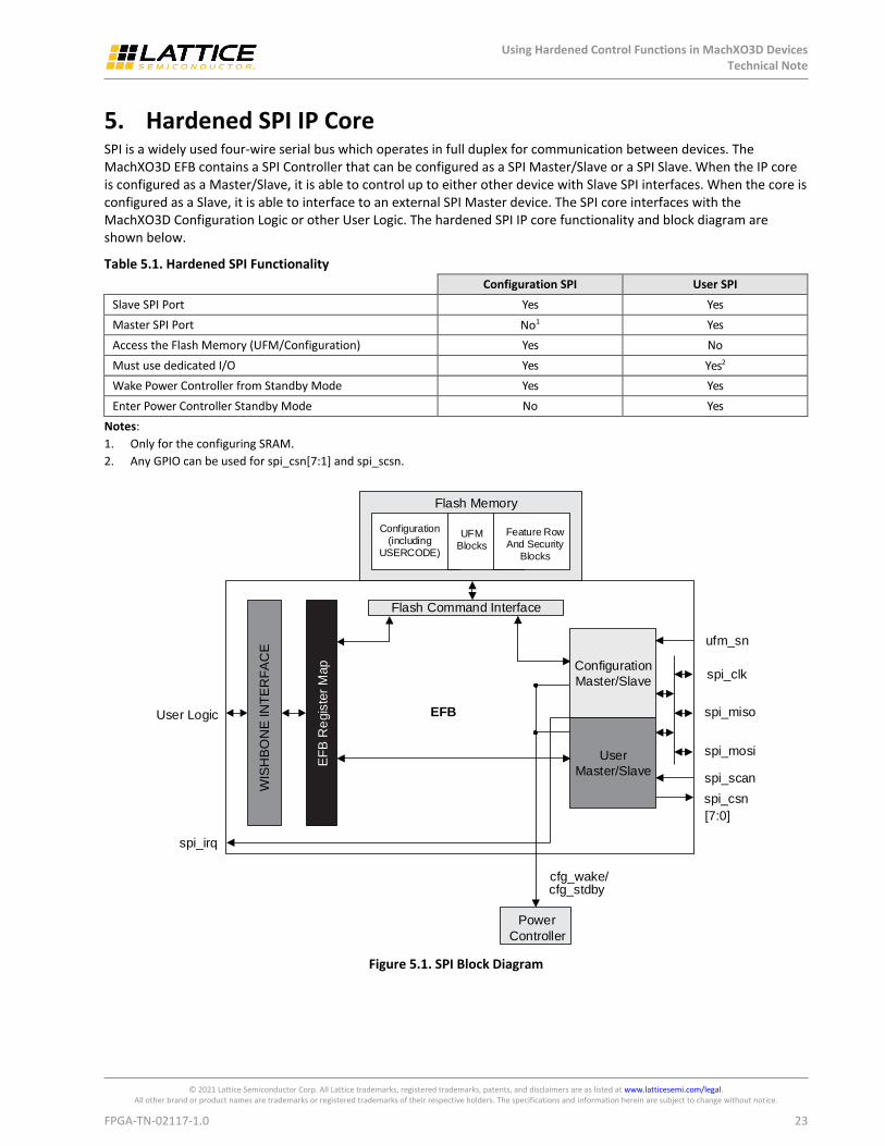
5. Hardened SPI IP Core SPI is a widely used four-wire serial bus which operates in full duplex for communication between devices. The MachXO3D EFB contains a SPI Controller that can be configured as a SPI Master/Slave or a SPI Slave. When the IP core is configured as a Master/Slave, it is able to control up to either other device with Slave SPI interfaces. When the core is configured as a Slave, it is able to interface to an external SPI Master device. The SPI core interfaces with the MachXO3D Configuration Logic or other User Logic. The hardened SPI IP core functionality and block diagram are shown below.
Table 5.1. Hardened SPI Functionality
Configuration SPI User SPI
Slave SPI Port Yes Yes
Master SPI Port No1 Yes
Access the Flash Memory (UFM/Configuration) Yes No
Must use dedicated I/O Yes Yes2
Wake Power Controller from Standby Mode Yes Yes
Enter Power Controller Standby Mode No Yes
Notes:
1. Only for the configuring SRAM.
2. Any GPIO can be used for spi_csn[7:1] and spi_scsn.
Configuration (including
USERCODE)
UFM Blocks
Flash Command Interface
Flash Memory
EF
B R
egis
ter
Map
WIS
HB
ON
E IN
TE
RF
AC
E
EFB
Power
Controller
spi_clk
Configuration
Master/Slave
User Logic
Feature RowAnd Security
Blocks
spi_miso
spi_irq
cfg_wake/cfg_stdby
Configuration
Master/Slave
User
Master/Slave
spi_mosi
ufm_sn
spi_scan
spi_csn
[7:0]
Figure 5.1. SPI Block Diagram

Using Hardened Control Functions in MachXO3D Devices Technical Note
© 2021 Lattice Semiconductor Corp. All Lattice trademarks, registered trademarks, patents, and disclaimers are as listed at www.latticesemi.com/legal. All other brand or product names are trademarks or registered trademarks of their respective holders. The specifications and information herein are subject to change without notice.
24 FPGA-TN-02117-1.0
The SPI IP core on MachXO3D devices support the following functions:
Configurable Master and Slave modes
Mode Fault error flag with CPU interrupt capability
Double-buffered data register for increased throughput
Serial clock with programmable polarity and phase
LSB First or MSB First Data Transfer
Interface to custom logic through the EFB WISHBONE slave interface
In Master/Slave SPI mode:
The User SPI controller has eight available Master Chip Selects (spi_csn[7:0]) ports. This allows the control of up to eight external devices with Slave SPI interface.
The Configuration SPI upon power-up, if the SPI port has been enabled to boot the MachXO3D device from an external Slave SPI Flash memory, then the SPI port acts as a Master SPI controller and spi_csn[0] is used as a Master Chip Select for selecting a specific SPI Flash memory. For information on Programming the MachXO3D through the SPI port, refer to the SPI section of MachXO3D Programming and Configuration Usage Guide (FPGA-TN-02069).
In Slave SPI mode:
The User SPI core has one Slave Chip Select (spi_scsn) pin. This allows the User SPI core to be selected by an external device with a Master SPI interface. User Logic is accessed through the EFB WISHBONE interface by a WISHBONE Master in the FPGA logic.
The Configuration SPI has one Slave Chip Select (ufm_sn) pin. An external SPI Master can access the MachXO3D’s Configuration Logic by asserting the chip select input. The external SPI Master can reprogram the MachXO3D Configuration Flash and User Flash Memory by performing bus transfers with SN asserted.
This usage guide is focused on the User SPI access. For more information on Programming the MachXO3D through SPI port reference, refer to the SPI section of MachXO3D Programming and Configuration Usage Guide (FPGA-TN-02069).
The Slave Configuration SPI port can be used to wake the Power Controller from Standby or enter Standby. The Slave User SPI port can only be used to wake the Power Controller from Standby mode. For more information on the Power Controller, refer to Power Estimation and Management for MachXO3D Devices. The SPI Power Controller features can be set up through IPexpress as documented later and the register settings are defined in Using Hardened Control Functions in MachXO3D Devices Reference Guide (FPGA-TN-02119).
5.1. SPI Interface Signals The SPI interface uses a serial transmission protocol. Data is transmitted serially (shifted out from the transmitting device) and it is received serially, shifted into the receiving device. The master device selects a specific slave device by asserting a chip select, enabling the slave device to shift in the commands/data and to respond by shifting out data.
Table 5.2 documents the signals that are associated with the IP core. Each signal has a description of the usage and how it should be connected in a design project.
Table 5.2. SPI – IP Signals
Signal Name
Pre-assigned Pin Name
I/O Width Description
spi_clk MCLK/CCLK Bi-directional 1 The signal is an output if the SPI core is in Master mode (MCLK). The signal is an input if the SPI core is in Slave mode (CCLK).
This signal must be brought to the top level of the user RTL design. The Diamond software automatically routes this signal to its Pre-Assigned pin (no user pin location constraint is necessary). Refer to the MachXO3D Family Datasheet (FPGA-DS-02026) pin tables for detailed pad and pin locations of SPI signals in each MachXO3D device.

Using Hardened Control Functions in MachXO3D Devices Technical Note
© 2021 Lattice Semiconductor Corp. All Lattice trademarks, registered trademarks, patents, and disclaimers are as listed at www.latticesemi.com/legal. All other brand or product names are trademarks or registered trademarks of their respective holders. The specifications and information herein are subject to change without notice.
FPGA-TN-02117-1.0 25
Signal Name
Pre-assigned Pin Name
I/O Width Description
spi_miso SPISO/SO Bi-directional 1 The signal is an input if the SPI core is in Master mode (SPISO). The signal is an output if the SPI core is in Slave mode (SO).
This signal must be brought to the top level of the user RTL design. The Diamond software automatically routes this signal to its Pre-Assigned pin (no user pin location constraint is necessary). Refer to the MachXO3D Family Datasheet (FPGA-DS-02026) pin tables for detailed pad and pin locations of SPI signals in each MachXO3D device.
spi_mosi SISPI/SI Bidirectional 1 The signal is an output if the SPI core is in Master mode (SISPI). The signal is an input if the SPI core is in Slave mode (SI).
This signal must be brought to the top level of the user RTL design. The Diamond software automatically routes this signal to its Pre- Assigned pin (no user pin location constraint is necessary). Refer to the MachXO3D Family Datasheet (FPGA-DS-02026) pin tables for detailed pad and pin locations of SPI signals in each MachXO3D device.
spi_csn[7:0] CSSPIN Output 8 Master Chip Select (Active Low) – Up to eight independent slave SPI devices can be accessed using the MachXO3D SPI Controller when it is in Master SPI mode.
The signal spi_csn[0] must be brought to the top level of the user RTL design. Diamond software automatically routes this signal to its Pre- Assigned pin (no user pin location constraint is necessary). Refer to the MachXO3D Family Datasheet (FPGA-DS-02026) tables for detailed pad and pin locations of SPI signals in each MachXO3D device.
spi_scsn — Input 1 User Slave Chip Select (Active Low) – An external SPI Master controller asserts this signal to transfer data to/from the SPI Controllers Transmit Data/Receive Data registers. The signal can be routed to any GPIO of MachXO3D device.
ufm_sn SN Input 1 Configuration Logic Chip select (Active Low) is dedicated for selecting the Flash Memory UFM and Configuration Sectors. This signal must be brought to the top level of the user RTL design. The Diamond software automatically routes this signal to its Pre-Assigned pin (no user pin location constraint is necessary). Refer to the MachXO3D Family Datasheet (FPGA-DS-02026) pin tables for detailed pad and pin locations of SPI signals in each MachXO3D device.
SN is an active pin whenever the SPI core is instantiated, even if the ufm_sn does not appear on the EFB primitive. Thus, SN cannot be recovered as user I/O. SN can be tied high externally to augment the weak internal pull-up if not connected to an external Master SPI bus.
SN is also active in a blank or erased device.
spi_irq — Output 1 Interrupt request output signal of the SPI core. This signal is intended to be connected to a WISHBONE master controller (that is by a microcontroller or state machine). It is asserted when specific conditions are met. These conditions controlled using the SPI register settings.
cfg_wake — Output 1 Wakeup signal – to be connected only to the Power Controller module of the MachXO3D device. The signal is enabled only if the Wakeup Enable feature has been set within the EFB user interface, SPI Tab.
cfg_stdby — Output 1 Stand-by signal – to be connected only to the Power Controller module of the MachXO3D device. The signal is enabled only if the Wakeup Enable feature has been set within the EFB user interface, SPI Tab.

Using Hardened Control Functions in MachXO3D Devices Technical Note
© 2021 Lattice Semiconductor Corp. All Lattice trademarks, registered trademarks, patents, and disclaimers are as listed at www.latticesemi.com/legal. All other brand or product names are trademarks or registered trademarks of their respective holders. The specifications and information herein are subject to change without notice.
26 FPGA-TN-02117-1.0
5.2. Configuring the SPI Core with IPexpress IPexpress is used to configure the SPI Controller and to generate Verilog or VHDL source code for inclusion in your design. Selecting the SPI tab, in the EFB user interface, displays the configurable settings for the SPI core. Figure 5.2 shows an example SPI Controller configuration.
Figure 5.2. Configuring the SPI Functions of the EFB Module with IPexpress
5.2.1. SPI Mode
This option allows you to select between Slave, or Slave & Master modes for the initial mode of the SPI core. Selecting Slave & Master enables SPI Master settings, which include Master Clock Rate and Master Chip Selects. This option can be updated dynamically by modifying the MSTR bit of the register SPICR2.
5.2.2. SPI Master Clock Rate
Desired Frequency
The EFB SPI Controller, when it is configured as an SPI Master, provides an output clock to the SPI Slave devices on the bus. The output frequency uses a power of two value to divide the WISHBONE Clock Frequency. The SPI Master uses the Master Clock Rate to time all SPI bus transactions and internal operations. The MachXO3D SPI Master interface can operate at speeds up to 45 MHz. Input the WISHBONE Clock Frequency on the EFB Enables tab of the dialog.
The divisor can be changed while the FPGA is in user mode. Updating the divider value in the SPIBR register causes the SPI Controller to reset and use a new output clock frequency.
Actual Frequency
It is not always possible to divide the input WISHBONE clock exactly to the requested frequency. The actual frequency value is returned in this read-only field. When both the desired SPI clock and WISHBONE clock fields have valid data and either is updated, this field returns the value rounded to two decimal places.

Using Hardened Control Functions in MachXO3D Devices Technical Note
© 2021 Lattice Semiconductor Corp. All Lattice trademarks, registered trademarks, patents, and disclaimers are as listed at www.latticesemi.com/legal. All other brand or product names are trademarks or registered trademarks of their respective holders. The specifications and information herein are subject to change without notice.
FPGA-TN-02117-1.0 27
5.2.3. SPI Protocol Options
LSB First
This setting specifies the order of the serial shift of a byte of data. The data order (MSB or LSB first) is programmable within the SPI core. This option can be updated dynamically by modifying the LSBF bit in the register SPICR2.
Inverted Clock
The inverts the clock polarity used to sample and output data is programmable for the SPI core. When selected, the edge changes from the rising to the falling clock edge. This option can be updated dynamically by accessing the CPOL bit of register SPICR2.
Phase Adjust
An alternate clock-data relationship is available for SPI devices with particular requirements. This option allows you to specify a phase change to match the application. This option can be updated dynamically by accessing the CPHA bit in the register SPICR2.
Slave Handshake Mode
Enables Lattice proprietary extension to the SPI protocol. This option is used when the internal support circuit (such as WISHBONE host) cannot respond with initial data within the time required, and to make the Slave read out data predictably available at high SPI clock rates. This option can be updated dynamically by accessing the SDBRE bit in the register SPICR2.
5.2.4. Master Chip Selects
The SPI Controller provides the ability to provide up to eight individual chip select outputs for master operation.
Each slave SPI device accessed by the master must have their own dedicated chip select. This option can be updated dynamically by modifying the register SPICSR.
5.2.5. SPI Controller Interrupts
TX Ready
An interrupt which indicates the SPI transmit data register (SPITXDR) is empty. The interrupt bit is
IRQTRDY of the register SPIIRQ. When enabled, indicates TRDY was asserted. Write a 1 to this bit to clear the interrupt. This option can be change dynamically by modifying the bit IRQTRDYEN in the register SPICSR.
RX Ready
An interrupt which indicates the receive data register (SPIRXDR) contains valid receive data. The interrupt is bit IRQRRDY of the register SPIIRQ. When enabled, indicates RRDY was asserted. Write a 1 to this bit to clear the interrupt. This option can be change dynamically by modifying the bit IRQRRDYEN in the register SPICSR.
TX Overrun
An interrupt which indicates the Slave SPI chip select (SPI_SCSN) was driven low while a SPI Master.
The interrupt is bit IRQMDF of the register SPIIRQ. When enabled, indicates MDF (Mode Fault) was asserted.
Write a 1 to this bit to clear the interrupt. This option can be changed dynamically by modifying the bit IRQMDFEN in the register SPICSR.
RX Overrun
An interrupt which indicates SPIRXDR received new data before the previous data. The interrupt is bit
IRQROE of the register SPIIRQ. When enabled, indicates ROE was asserted. Write a 1 to this bit to clear the interrupt. This option can be change dynamically by modifying the bit IRQROEEN in the register SPICSR.

Using Hardened Control Functions in MachXO3D Devices Technical Note
© 2021 Lattice Semiconductor Corp. All Lattice trademarks, registered trademarks, patents, and disclaimers are as listed at www.latticesemi.com/legal. All other brand or product names are trademarks or registered trademarks of their respective holders. The specifications and information herein are subject to change without notice.
28 FPGA-TN-02117-1.0
Enable Port (Interrupts)
This enables the interrupt request output signal (spi_irq_ of the SPI core signal). This signal is intended to be connected to a WISHBONE master controller (that is by a microcontroller or state machine) and to request an interrupt when a specific condition is met.
5.2.6. Wake-up Enable
Enables the SPI core to send a wake-up signal to the Power Controller to wake the part from standby mode when the User Slave SPI chip select (spi_csn[0]) is driven low. This option can be updated dynamically by modifying the bit WKUPEN_USER in the register SPICR1.
5.2.7. MachXO3D SPI Usage Cases
Refer to Figure 5.3, Figure 5.4, and Figure 5.5 for the SPI usage cases described below.
External Master SPI Device accessing the Slave MachXO3D User SPI:
The External Master SPI is connected to the MachXO3D using the dedicated SI, SO, CCLK pins. The spi_scsn is placed on any Generic I/O. The EFB SPI Mode is set to Slave only.
A WISHBONE Master controller is implemented in the MachXO3D general purpose logic array. The master controller monitors the availability to transmit or receive data by polling the SPI status registers, or by responding to interrupts generated by the SPI Controller. For information on the SPI register definitions and command sequences, reference the SPI section of Using Hardened Control Functions in MachXO3D Devices Reference Guide (FPGA-TN-02119).
The external SPI Master does not have access to the MachXO3D Configuration Logic because the SN that selects the Configuration Logic is pulled high.
Figure 5.3. External Master SPI Device Accessing the Slave MachXO3D User SPI
MachXO3D User SPI Master accessing one or multiple External Slave SPI devices:
The MachXO3D SPI Master is connected to External SPI Slave devices using the dedicated SPI port pins. The Chip Selects are configured as follows:
The MachXO3D SPI Master Chip Select spi_scn[0] is placed on the dedicated CSSPIN and connected to the External Slave Chip Select.
The MachXO3D SPI Master Chip Select spi_scn[1] is placed on any I/O and connected to another External Slave Chip Select.
Up to eight External Slave SPIs can be connected using spi_scn[7:0]

Using Hardened Control Functions in MachXO3D Devices Technical Note
© 2021 Lattice Semiconductor Corp. All Lattice trademarks, registered trademarks, patents, and disclaimers are as listed at www.latticesemi.com/legal. All other brand or product names are trademarks or registered trademarks of their respective holders. The specifications and information herein are subject to change without notice.
FPGA-TN-02117-1.0 29
A WISHBONE Master controller is implemented in the MachXO3D general logic. It controls transfers to the slave SPI devices. It can use a polling method, or it can use SPI Controller interrupts to manage transfer and reception of data.
For information on the SPI register definitions and command sequences, reference the SPI section of Using Hardened Control Functions in MachXO3D Devices Reference Guide (FPGA-TN-02119).
MCLK
SISPI
SPISO
CSSPIN
(any GPIO)
(any GPIO)
Figure 5.4. MachXO3D User SPI Master Accessing One or Multiple External Slave SPI Devices
External Master SPI Device accessing the MachXO3D Configuration Logic
The External SPI Master is connected to the MachXO3D dedicated slave Configuration SPI port pins. The external SPI Master chip select controls the SN input that enables the MachXO3D Configuration Logic block. The external master sends commands to the Configuration Logic block permitting it to interface to the Configuration Flash and the UFM.
For information on accessing the Flash Memory (UFM/Configuration) of the MachXO3D device through SPI, it can be found later in this document.
For more information on Programming the MachXO3D through SPI port reference, refer to the SPI section of MachXO3D Programming and Configuration Usage Guide (FPGA-TN-02069).
Figure 5.5. External Master SPI Device Accessing the MachXO3D Configuration Logic

Using Hardened Control Functions in MachXO3D Devices Technical Note
© 2021 Lattice Semiconductor Corp. All Lattice trademarks, registered trademarks, patents, and disclaimers are as listed at www.latticesemi.com/legal. All other brand or product names are trademarks or registered trademarks of their respective holders. The specifications and information herein are subject to change without notice.
30 FPGA-TN-02117-1.0
5.2.8. SPI Design Tips For information on the SPI register definitions and command sequences, refer to the SPI section of Using Hardened
Control Functions in MachXO3D Devices Reference Guide (FPGA-TN-02119).
Take note when dynamically turning off components for power savings; the EFB requires the MachXO3D internal oscillator to be enabled even if it is not the source of the WISHBONE Clock. The exception is with User Slave or User Master modes.
The SPI bus is bidirectional. A byte is received for every byte transmitted. Always discard RX data to avoid Receiver Overrun Error (ROE).
SN is an active pin whenever the SPI core is instantiated, whether ufm_sn appears on the EFB primitive or not. Thus, SN cannot be recovered as user I/O. SN should be tied high externally to augment the weak internal pull-up if not connected to an external Master SPI bus.
There are a number of SPI reference designs on the Lattice website (www.latticesemi.com/products/intellectualproperty/aboutreferencedesigns.cfm) including:
SPI Slave Peripheral using Embedded Function Block
MachXO2 Hardened SPI Master/Slave Demo (UG56)

Using Hardened Control Functions in MachXO3D Devices Technical Note
© 2021 Lattice Semiconductor Corp. All Lattice trademarks, registered trademarks, patents, and disclaimers are as listed at www.latticesemi.com/legal. All other brand or product names are trademarks or registered trademarks of their respective holders. The specifications and information herein are subject to change without notice.
FPGA-TN-02117-1.0 31
6. Timer/Counter The MachXO3D EFB contains a Timer/Counter function. This Timer/Counter is a general purpose 16-bit Timer/Up Down Counter module with independent output compare units and Pulse Width Modulation (PWM) support. The Timer/Counter supports the following functions:
Four unique modes of operation:
Watchdog timer
Clear Timer on Compare Match
Fast PWM
Phase and Frequency Correct PWM
Programmable clock input source
Programmable input clock pre-scale
Interrupt output to FPGA fabric
Three independent interrupt sources: overflow, output compare match, and input capture
Auto reload
Time-stamping support on the input capture unit
Waveform generation on the output
Glitch-free PWM waveform generation with variable PWM period
Internal WISHBONE bus access to the control and status registers
Stand-alone mode with preloaded control registers and direct reset input
EF
B R
eg
iste
r M
ap
WIS
HB
ON
E IN
TE
RF
AC
E
EFB
User Logic
tc_oc
tc_int
tc_ic
tc_rstn
tc_clki
TCTOPSET TCTOP
TCOCRSET
TCOCR
TCICR
TCCR0,1,2
TCSR0
TCIRQ
TCIRQEN
16-BitCounter
TCCNT
Timer/ Counter
Logic
PRESCALE
Timer/Counter
Figure 6.1. Timer/Counter Block Diagram
The Timer/Counter communicates with the FPGA core logic through the WISHBONE interface and specific signals such as clock, reset, interrupt, timer output, and event trigger. The Timer/Counter can be included in a design with or without the WISHBONE interface.

Using Hardened Control Functions in MachXO3D Devices Technical Note
© 2021 Lattice Semiconductor Corp. All Lattice trademarks, registered trademarks, patents, and disclaimers are as listed at www.latticesemi.com/legal. All other brand or product names are trademarks or registered trademarks of their respective holders. The specifications and information herein are subject to change without notice.
32 FPGA-TN-02117-1.0
6.1. Timer/Counter Modes of Operation The Timer/Counter is a flexible function, which has four modes of operation. These modes are designed to meet different system needs related to sequencing of events and PWM (Pulse Width Modulation). The four Timer/Counter modes are:
Clear Timer on Compare Match
Watchdog Timer
Fast PWM
Phase and Frequency Correct PWM
6.1.1. Clear Timer on Compare Match Mode
CTCM (Clear Timer on Compare Match) is a basic counter with interrupts. The counter is automatically cleared to 0x0000 when the counter value, TCCNT register, matches the value loaded in the TCTOP register. The value of the TCTOP register can by dynamically be updated through the WISHBONE register, or it can hold a static value that is assigned with IPexpress at the time of IP generation. The default value of the TCTOP register is 0xFFFF.
The data loaded into the timer counter to define the top counter value is double-registered. The WISHBONE host writes the data to TCTOPSET register, which is then automatically loaded onto the TCTOP register at the moment of auto-clear. Therefore, a new top value can be written to the TCTOPSET register after the overflow flag and during the counting-up to the top value. Updating the value of the TCTOP register changes the frequency of the output signal of the Timer/Counter.
Figure 6.2. Timer/Counter Output Waveform
6.1.2. Watchdog Timer Mode
Watchdog timers are used to monitor a system operating behavior and to provide a reset or interrupt when the system microcontroller or embedded state machine is no longer operational. One scenario is for a microcontroller to reset the Watchdog Timer to 0x0000 before it begins a process. The microcontroller must complete the process and reset the Watchdog Timer before the timer reaches its terminal count. In the event that the microprocessor does not clear the timer quickly enough the Watchdog Timer asserts a strobe signaling time expired. The system uses the time exceeded strobe to gracefully recover the system.
Another way to use the Watchdog Timer is to periodically turn OFF system modules in order to save power. It can also be used to interact with the on-chip power controller of the MachXO3D device.
The most commonly used ports of the Timer/Counter in Watchdog Timer Mode are the clock, reset and interrupt.
Optionally, the WISHBONE interface can be used to read time stamps from the TCICR register and update the top value of the counter.
OC
CNT
OVF
Period 3Period 2
Top
Period 1 Period 4
0 1 Top 0 1 Top 0 1Counting Up Counting Up

Using Hardened Control Functions in MachXO3D Devices Technical Note
© 2021 Lattice Semiconductor Corp. All Lattice trademarks, registered trademarks, patents, and disclaimers are as listed at www.latticesemi.com/legal. All other brand or product names are trademarks or registered trademarks of their respective holders. The specifications and information herein are subject to change without notice.
FPGA-TN-02117-1.0 33
6.1.3. Fast PWM Mode
Pulse-Width Modulation (PWM) is a popular technique to digitally control analog circuits. PWM uses a rectangular pulse wave whose pulse width is modulated resulting in the variation of the average value of the waveform. You can vary the period and the duty cycle of the waveform by loading 16-bit digital values on the TCTOP register to define the top value of the counter, and the TCOCR register to provide a compare value for the output of the counter.
The output of the Timer/Counter is cleared when the counter value matches the top value that is loaded in the TCTOP register. The output is set when the value of the counter matches the compare value that is loaded into the TCOCR register. The clear/set functions can be inverted. This means that the output of the Timer/Counter is set when the counter value matches the top value and it is cleared when the value of the counter matches the compare value.
The interrupt line can be used for Overflow Flag (OVF) and Output Compare Flag (OCRF).
Figure 6.3 shows the PWM waveform generation. The output of the Timer/Counter is configured to be set when the counter matches the top value and clear when the counter matches the compare value.
OC
CNT
OVF
Period 3Period 2Period 1 Period 4
...
OCRF
Top 0 1 ... ocrocr
+1Top 0 1 ... ocr
ocr
+1... Top 0 1
Figure 6.3. PWM Waveform Generation
6.1.4. Phase and Frequency Correct PWM Mode
In phase and frequency correct PWM mode, the counting direction changes from up to down at the moment the counter is incrementing to the top value (top value minus 1). The moment that the counter is decrementing from 0x0001 to 0x0000, the following occurs:
TCTOP is updated with the value loaded in the TCTOPSET register
TCOCR is updated with the value loaded in the TCOCRSET register
Overflow TCSR[OVF] is asserted for one clock cycle
The output of the Timer/Counter is updated only when the counter value matches the compare value in TCOCR register. This occurs twice within one period. The first match occurs when the counter is counting up and the second match occurs when the counter is counting down. The Output Compare Flag TCSR[OCRF] is asserted when both matches occur. The output of the Timer/Counter is set on the first compare match and cleared on the second compare match. The order of set and clear can be inverted.
The mode allows you to adjust the frequency (based on the top value) and phase (based on the compare value) of the generated waveform.

Using Hardened Control Functions in MachXO3D Devices Technical Note
© 2021 Lattice Semiconductor Corp. All Lattice trademarks, registered trademarks, patents, and disclaimers are as listed at www.latticesemi.com/legal. All other brand or product names are trademarks or registered trademarks of their respective holders. The specifications and information herein are subject to change without notice.
34 FPGA-TN-02117-1.0
OC
CNT
OVF
Period 2Period 1 Period 3
... ... ...
OCRF
Counting
UP
Counting
DOWNDirection
0 11 0 11ocrocr
+1top-1 top top-1... ocr ocr-1
Figure 6.4. Phase and Frequency Correct PWM Waveform Generation
6.2. Timer/Counter IP Signals Table 6.1 documents the signals that are generated with the IP. Each signal has a description of the usage and how it should be connected in a design project.
Table 6.1. Timer/Counter – IP Signals
Signal Name I/O Width Description
tc_clki Input 1 Timer/Counter input clock signal can be connected to the on-chip oscillator. The clock signal is limited to 133 MHz.
tc_rstn Input 1 This is an active-low reset signal, which resets the 16-bit counter.
tc_ic Input 1
This is an active-high input capture trigger event, applicable for non-PWM modes with WISHBONE interface. If enabled, a rising edge of this signal is detected and synchronized to capture the counter value (TCCNT Register) and make the value accessible to the WISHBONE interface by loading it into TCICR register. The common usage is to perform a time-stamp operation with the counter.
tc_int Output 1 This is an interrupt signal, indicating the occurrence of a specific event such as Overflow, Output Compare Match, or Input Capture.
tc_oc Output 1 Timer/Counter output signal
6.3. Configuring the Timer/Counter IPexpress is used to configure the Timer/Counter. Selecting the Timer/Counter tab in the EFB user interface displays the configurable settings of the Timer/Counter core.
The Timer/Counter can be used with or without the WISHBONE interface. For usage without the WISHBONE interface, you can select/enter values in the IPexpress EFB user interface. The values are programmed in the Timer/Counter registers with the programmable bitstream. Using the Timer/Counter with a WISHBONE interface enables you to dynamically update the register content through the WISHBONE interface. The main EFB user interface, EFB Enables tab, allows you to make a selection between using the Timer/Counter with or without a WISHBONE screen shot.
Figure 6.5 shows an example of the Timer/Counter is configured for a specific design.

Using Hardened Control Functions in MachXO3D Devices Technical Note
© 2021 Lattice Semiconductor Corp. All Lattice trademarks, registered trademarks, patents, and disclaimers are as listed at www.latticesemi.com/legal. All other brand or product names are trademarks or registered trademarks of their respective holders. The specifications and information herein are subject to change without notice.
FPGA-TN-02117-1.0 35
Figure 6.5. Configuring the Timer/Counter
6.3.1. Timer/Counter Mode
This option allows you to select one of the four operating modes.
CTCM – Clear Timer on Compare Match
WATCHDOG – Watchdog timer
FASTPWM – Fast PWM
PFCPWM – Phase and Frequency Correct PWM
This option can be updated dynamically by modifying the bits TCM[1:0] of the register TCCR1.
6.3.2. Output Function
You can select the function of the output signal (tc_oc) of the Timer/Counter IP. The available functions are:
STATIC – The output of the Timer/Counter is static low.
TOGGLE – The output of the Timer/Counter toggles based on the conditions defined by the Timer/Counter Mode.
WAV_GENERATE – The waveform is generated by the Set/Clear on the conditions defined by the Timer/Counter Mode.
INV_WAV_GENERATE – The waveform is inverted.
This option can be updated dynamically by modifying bits OCM[1:0] of the register TCCR1.
6.3.3. Clock Edge Selection
You can select the edge (positive or negative) of the input clock source as well as enable the usage of the on-chip oscillator. The selections are:
PCLOCK – Positive edge of the clock from user logic.
POSC – Positive edge of the clock from the internal oscillator.
NCLOCK – Negative edge of the clock from user logic.
NOSC – Negative edge of the clock from the internal oscillator.
This option can be updated dynamically by modifying the bits CLKSEL and CLKEDGE of the register TCCR0.

Using Hardened Control Functions in MachXO3D Devices Technical Note
© 2021 Lattice Semiconductor Corp. All Lattice trademarks, registered trademarks, patents, and disclaimers are as listed at www.latticesemi.com/legal. All other brand or product names are trademarks or registered trademarks of their respective holders. The specifications and information herein are subject to change without notice.
36 FPGA-TN-02117-1.0
6.3.4. Pre-scale Divider Value
Pre-scale divider values (0, 1, 8, 64, 256, 1024) are provided to divide the input clock prior to reaching the 16-bit counter. This option can be updated dynamically by modifying the bits PRESCALE[2:0] of the register TCCR1.
6.3.5. Timer/Counter Top
You can select the top value of the counter. This option can be updated dynamically by modifying the bits TCTOPSET of the registers TCTOPSET1 and TCTOPSET0.
6.3.6. Output Compare Value
You can select the output compare value of the counter. This option can be updated dynamically by modifying the bits TCOCRSET the registers TCOCRSET1 and TCOCRSET0.
6.3.7. Enable Interrupt Registers Overflow – An interrupt which indicates the counter matches the TCTOP0/1 register value. The interrupt is bit
IRQOVF of the register TCIRQ. When enabled, indicates OVF was asserted. Write a 1 to this bit to clear the interrupt. This option can be updated dynamically by modifying the bit IRQOVFEN of the register TCIRQEN.
Output Compare Match – An interrupt which indicates when counter matches the TCOCR0/1 register value. The interrupt is bit IRQOCRF of the register TCIRQ. When enabled, indicates OCRF was asserted. Write a 1 to this bit to clear the interrupt. This option can be updated dynamically by modifying the IRQOCRFEN bit of register TCIRQEN.
Input Capture – An interrupt which indicates when you assert the TC_IC input signal. The interrupt is bit IRQICRF of the register TCIRQ. When enabled, indicates ICRF was asserted. Write a 1 to this bit to clear the interrupt. This option can be updated dynamically by modifying IRQICRFEN bit of the register TCIRQEN.
Standalone Overflow – Used without the WISHBONE interface and serves as the only available interrupt request.
6.3.8. MachXO3D Timer/Counter Usage Cases
6.3.8.1. Basic counter with interrupts
Configure the Timer/Counter for Static or Dynamic operation. Dynamic operation enables the WISHBONE bus interface allowing a WISBONE Master to control the Timer/Counter.
To configure the Timer/Counter for Static or Dynamic operation in the Timer Counter tab:
1. Configure the Timer/Counter Mode using the Mode Selection controls:
a. Select CTCM (Clear Timer on Compare Match) Mode.
b. Select the Output Function:
Hold static 0 (STATIC)
Toggle (TOGGLE)
2. Update the Clock Selections
a. Select the clock edge to which the Timer/Counter responds.
Positive (PCLOCK) or Negative (NCLOCK) edge
b. Select the Clock Pre-scale Divider.
3. Configure the Counter Values
a. Enable the Top Counter Value.
b. Select a Timer/Counter Top value.
4. Enable optional interrupts

Using Hardened Control Functions in MachXO3D Devices Technical Note
© 2021 Lattice Semiconductor Corp. All Lattice trademarks, registered trademarks, patents, and disclaimers are as listed at www.latticesemi.com/legal. All other brand or product names are trademarks or registered trademarks of their respective holders. The specifications and information herein are subject to change without notice.
FPGA-TN-02117-1.0 37
6.3.8.2. Watchdog Timer
Configure the Timer/Counter for Static or Dynamic operation. Dynamic operation enables the WISHBONE
bus interface allowing a WISBONE Master to control the Timer/Counter.
To configure the Timer/Counter for Static or Dynamic operation in the Timer Counter tab:
1. Configure the Timer/Counter Mode using the Mode Selection controls
a. Select WATCHDOG mode.
b. Select Output Function:
Hold static 0 (STATIC)
2. Update the Clock Selections:
a. Select the clock edge to which the Timer/Counter responds:
Positive (PCLOCK) or Negative (NCLOCK) edge
b. Select the Clock Pre-scale Divider.
3. Configure the Counter Values
a. Enable the Top Counter Value.
b. Select a Timer/Counter Top value.
c. Select an Output Compare Value.
4. Enable interrupts (TC_INT)
a. Select Output Compare Match.
b. Select Input Capture.
6.3.8.3. PWM Output with variable duty cycle and period
Configure the Timer/Counter for Static or Dynamic operation. Dynamic operation enables the WISHBONE
bus interface allowing a WISBONE Master to control the Timer/Counter.
To configure the Timer/Counter for Static or Dynamic operation in the Timer Counter tab:
1. Configure the Timer/Counter Mode using the Mode Selection controls:
a. Select the FASTPWM mode.
b. Select Output Function:
Hold static 0 (STATIC)
PWM (WAVE_GENERATOR)Complement PWM (INV_WAVE_GENERATOR)
2. Update the Clock Selections:
a. Select the clock edge to which the Timer/Counter responds:
Positive (PCLOCK) or Negative (NCLOCK) edge
b. Select the Clock Pre-scale Divider.
3. Configure the PWM Values
a. Select the PWM period (Timer Counter Top).
b. Select the PWM duty cycle (Output Compare Value):
Where the duty cycle is (Output Compare Value)/(Timer Counter Top): [(Timer CounterTop) – (Output Compare Value)]/(Timer Counter Top)

Using Hardened Control Functions in MachXO3D Devices Technical Note
© 2021 Lattice Semiconductor Corp. All Lattice trademarks, registered trademarks, patents, and disclaimers are as listed at www.latticesemi.com/legal. All other brand or product names are trademarks or registered trademarks of their respective holders. The specifications and information herein are subject to change without notice.
38 FPGA-TN-02117-1.0
6.3.8.4. PWM output with 50:50 duty variable phase and period
Configure the Timer/Counter for Static or Dynamic operation. Dynamic operation enables the WISHBONE bus interface allowing a WISBONE Master to control the Timer/Counter.
To configure the Timer/Counter for Static or Dynamic operation in the Timer Counter tab:
1. Configure the Timer/Counter Mode using the Mode Selection controls:
a. Select FASTPWM.
b. Select Output Function:
Hold static 0 (STATIC)
PWM (WAVE_GENERATOR)
Complement PWM (INV_WAVE_GENERATOR)
2. Update the Clock Selections:
a. Select the clock edge to which the Timer/Counter responds:
Positive (PCLOCK) or Negative (NCLOCK) edge
b. Select the Clock Pre-scale Divider.
3. Configure the PWM Values:
a. Select the PWM period (Timer Counter Top).
b. Select the Phase Adjustment (Output Compare Value):
Where Phase Adjustment is (360 degrees) × (Output Compare Value) / (Timer Counter Top)
6.3.9. Timer/Counter Design Tips For information on the Timer/Counter register definitions and command sequences, refer to the Timer/Counter
section of Using Hardened Control Functions in MachXO3D Devices Reference Guide (FPGA-TN-02119).
Take note when dynamically turning off components for power savings; the EFB requires the MachXO3D internal oscillator to be enabled even if it is not the source of the WISHBONE Clock. The exception is when the user clock is selected.

Using Hardened Control Functions in MachXO3D Devices Technical Note
© 2021 Lattice Semiconductor Corp. All Lattice trademarks, registered trademarks, patents, and disclaimers are as listed at www.latticesemi.com/legal. All other brand or product names are trademarks or registered trademarks of their respective holders. The specifications and information herein are subject to change without notice.
FPGA-TN-02117-1.0 39
7. Flash Memory (UFM/Configuration) Access You can access the Flash Memory Configuration Logic interface using the JTAG, SPI, I2C, or WISHBONE interfaces. The MachXO3D Flash Memory consists of multiple memory sub-sectors:
Two configuration memory sectors (CFG0 and CFG1)
Four user flash memory sectors (UFM0, 1, 2, and 3)
One feature row sector (FEA)
One public key sector (PUBKEY)
One Advanced Encryption Standard Key sector (AESKEY)
One configuration security setting sector (CSEC)
One user security setting sector (USEC)
Refer to the MachXO3D Programming and Configuration Usage Guide (FPGA-TN-02069) for more implementation details.
The ports to access the Flash Memory and the block diagram are shown in Table 7.1.
Table 7.1. Flash Memory (UFM/Configuration) Access
UFM Configuration Flash
JTAG Yes Yes
Slave SPI Port with Chip Select (ufm_sn) Yes Yes
Slave SPI Port with Chip Select (spi_scsn) No No
Primary Slave I²C Port address (yyyxxxxx00) Yes Yes
Primary Slave I²C Port address (yyyxxxxx01) No No
Secondary Slave I2C Port address (yyyxxxxx10) No No
WISHBONE Yes Yes
Configuration (including
USERCODE)
UFM Blocks
Flash Command Interface
Flash Memory
EF
B R
egis
ter
Map
Configuration
Master/SlaveWIS
HB
ON
E IN
TE
RF
AC
E
EFB
SPI Port
ufm_sn
Primary I²C Port
(Address yyyxxxxx00) Configuration
Slave
User Logic
JTAG
Feature Row and Security Blocks
Figure 7.1. Flash Memory (UFM/Configuration) Block Diagram

Using Hardened Control Functions in MachXO3D Devices Technical Note
© 2021 Lattice Semiconductor Corp. All Lattice trademarks, registered trademarks, patents, and disclaimers are as listed at www.latticesemi.com/legal. All other brand or product names are trademarks or registered trademarks of their respective holders. The specifications and information herein are subject to change without notice.
40 FPGA-TN-02117-1.0
8. Flash Memory (UFM/Configuration) Access Ports The Configuration Logic arbitrates access to the Flash Memory from the interfaces by the following priority. When higher priority ports are enabled, Flash Memory access by lower priority ports is blocked.
JTAG Port – All MachXO3D devices have a JTAG port, which can be used to perform Read/Write operations to the Flash Memory (UFM/Configuration). The JTAG port is compliant with the IEEE 1149.1 and IEEE 1532 specifications. JTAG has the highest priority to the Flash Memory (UFM/Configuration).
Slave SPI Port – All MachXO3D devices have a Slave SPI port, which can be used to perform Read/Write operations to the Flash Memory (UFM/Configuration). Asserting the Flash Memory (UFM/Configuration) Slave Chip Select (ufm_sn) enables access.
I2C Primary Port – All MachXO3D devices have an I2C port, which can be used to perform Read/Write operations to the NVCM/Flash. The Primary I²C Port address is yyyxxxxx00 (Where y and x are user programmable).
WISHBONE Slave Interface – The WISHBONE Slave interface of the EFB module enables you to access the Flash Memory (UFM/Configuration) from the FPGA user logic by creating a WISHBONE Master. In addition to the WISHBONE bus signals, an interrupt request output signal is brought to the FPGA fabric. An IRQ (wbc_ufm_irq) is provided to assist the WB Master to perform UFM/CF programming operations. It is configurable and provides information about the R/W FIFO, and arbitration errors.
Note: Enabling the Flash Memory (UFM/Configuration) Interface using Enable Configuration Interface command 0x74 Transparent Mode temporarily disables certain features of the device including:
Power Controller
GSR
Hardened User SPI Port
Hardened Primary User I²C Port
Functionality is restored after the Flash Memory (UFM/Configuration) Interface is disabled using Disable Configuration Interface command 0x26 followed by Bypass command 0xFF.

Using Hardened Control Functions in MachXO3D Devices Technical Note
© 2021 Lattice Semiconductor Corp. All Lattice trademarks, registered trademarks, patents, and disclaimers are as listed at www.latticesemi.com/legal. All other brand or product names are trademarks or registered trademarks of their respective holders. The specifications and information herein are subject to change without notice.
FPGA-TN-02117-1.0 41
9. Interface to UFM MachXO3D devices provide four sectors of User Flash Memory (UFM0, 1, 2, and 3). You can access the UFM sectors through the Configuration Logic interface using the JTAG, Configuration SPI, Primary Configuration I²C or WISHBONE interfaces. The UFM sectors are separate sectors within the on-chip Flash Memory and are organized by pages. In addition, the CFG sectors can be used as UFM if they are unused for configuration. For details on the page sizes and addressing, refer to Table 9.1 and the MachXO3D Programming and Configuration Usage Guide (FPGA-TN-02069).
Table 9.1. UFM Resources in MachXO3D Devices
UFM0 UFM1 UFM2 UFM3 CFG0* CFG1*
XO3D-4300
Bits 98,176 98,176 147,200 24,448 737,024 737,024
Bytes 12,272 12,272 18,400 3,056 92,128 92,128
Pages 767 767 1,150 191 5,758 5,758
XO3D-9400
Bits 458,496 458,496 147,200 24,448 1,605,248 1,605,248
Bytes 57,312 57,312 18,400 3,056 200,656 200,656
Pages 3,582 3,582 1,150 191 12,541 12,541 *Note: Reclaimed CFG sectors used as UFM.
The UFM is a general purpose Flash Memory. Refer to MachXO3D Family Datasheet (FPGA-DS-02026) for the number of Programming/Erase Specifications. The UFM is typically used to store system-level data, Embedded Block RAM initialization data, or executable code for microprocessors and state-machines. Use the following tools to partition the
UFM resource:
IPexpress – Use IPexpress to enable the UFM and to initialize the memory.
Spreadsheet View (Diamond) – The global sysConfig configuration options control the use of the UFM. Read MachXO3D Programming and Configuration Usage Guide (FPGA-TN-02069) for a complete description of available options.
9.1. Initializing the UFM with IPexpress You can initialize the UFM sector with system level non-volatile data and generate the EFB module via IPexpress. Selecting the UFM tab in the EFB user interface displays the configurable settings of the UFM.
Figure 9.1. Initializing the UFM Sector with IPexpress

Using Hardened Control Functions in MachXO3D Devices Technical Note
© 2021 Lattice Semiconductor Corp. All Lattice trademarks, registered trademarks, patents, and disclaimers are as listed at www.latticesemi.com/legal. All other brand or product names are trademarks or registered trademarks of their respective holders. The specifications and information herein are subject to change without notice.
42 FPGA-TN-02117-1.0
You enter the number of pages to be pre-loaded with initialization data. Because initialization data is bottom justified, the read-only field Initialization Data Starts at Page informs the designer with the address of the first page that is initialized. In the example used for this document, 512 pages of the UFM0 sector of MachXO3D-10000 are to be initialized with the content of the memory file example.mem.
UFM0 Utilization Example (MachXO3D-9400)
Initializing 512 Pages
Page 3582
...
...
Page 129
Last Page of Initial Data
First Page of Initial Data
Uninitialized Pages
Page 128
Page 1
Page 0
.
The MachXO3D-9400 device has 3582 pages in the UFM0 sector. The initialization data occupies the bottom (highest) addressable pages of the UFM, while the top (lowest) addressable pages remain uninitialized (all zeros). The format of the memory file is page-based and can be expressed in binary or hexadecimal format.
9.1.1. UFM Initialization Memory File
The initialization data file has the following properties and format:
Extension: .mem Format: Binary, Hexadecimal Data Width: 1 page (128 bits in one row of the file) No. of Rows: Less than or equal to the number of available pages
Example 1. Binary 1010…1010 (Placed at the starting page of the UFM initialization data, address = N) 1010…1010 (page address = N + 1) 1010…1010 (page address = N + 2)
…
1010…1010 (Placed at the highest UFM page address)
Example 2. Hexadecimal A…B (Placed at the starting page of the UFM initialization data, address = N) C…D (page address = N + 1) E…F (page address = N + 2)
…
A…F (Placed at the highest UFM page address)
The most significant byte (byte 15) of the page is on the left side of the row. The least significant byte of the page (byte 0) is on the right side of the row bit in a row is the left-most (that is by bit 127), the least significant is right-most (bit 0).
9.1.2. EBR Initialization
For designers that choose to share the UFM sector with EBR initialization data, the sector map below should be referenced as an example when planning the design. Note at this time the EBR Mapping is not supported in Diamond.

Using Hardened Control Functions in MachXO3D Devices Technical Note
© 2021 Lattice Semiconductor Corp. All Lattice trademarks, registered trademarks, patents, and disclaimers are as listed at www.latticesemi.com/legal. All other brand or product names are trademarks or registered trademarks of their respective holders. The specifications and information herein are subject to change without notice.
FPGA-TN-02117-1.0 43
UFM0 Sector
(MachXO3D-9400)
Page 3582
Page 146
Page 145 (EBR Block M Initialization Data)
Page 74 (EBR Block M Initialization Data)
Page 72 (EBR Block N Initialization Data)
Page 1 (EBR Block N Initialization Data)
Page 73 (EBR Block M Location)
Page 0 (EBR Block N Location)
...
...
...
...
Pages Available for
General Purpose
Non-volatile Data
Block M Location
and Initialization
Data
Block N Location
and Initiliazation
Data
Care must be taken when performing a Bulk-Erase operation to prevent the loss of EBR initialization data. Prior to erasing the UFM sector, you should make a copy of the pages holding the EBR block location and EBR initialization data in a secondary memory resource. After the UFM sector is erased, the data can be written back into the UFM. Upon power-up or a reconfiguration command, the EBR initialization data is automatically loaded in their respective EBR blocks. The EBR Block Location data guides the configuration logic on the location of the EBR block.
9.1.3. UFM in Lattice Diamond Software
The UFM sectors are one of the Flash Memory resources of the MachXO3D device. The CONFIGURATION option in the Diamond Spreadsheet view controls how UFM behaves (options are CFG, EXTERNAL, CFGUFM, or CFG_EBRUFM).

Using Hardened Control Functions in MachXO3D Devices Technical Note
© 2021 Lattice Semiconductor Corp. All Lattice trademarks, registered trademarks, patents, and disclaimers are as listed at www.latticesemi.com/legal. All other brand or product names are trademarks or registered trademarks of their respective holders. The specifications and information herein are subject to change without notice.
44 FPGA-TN-02117-1.0
10. Configuration Flash Memory The WISHBONE interface of the EFB module allows a WISHBONE master to access the Configuration resources of MachXO3D devices. This is particularly useful for reading data from Configuration resources such as USERCODE and TraceID. A WISHBONE master can update the Configuration Flash memory using the Configuration Logic transparent mode. The new design is active after power-up or a Configuration Refresh operation.
For more information on Programming the MachXO3D, refer to MachXO3D Programming and Configuration Usage Guide (FPGA-TN-02069) and Using Hardened Control Functions in MachXO3D Devices Reference Guide (FPGA-TN-02119).
Table 10.1. Configuration Flash Resources in MachXO3D Devices
CFG0 CFG1
XO3D-4300
Bits 737,024 737,024
Bytes 92,128 92,128
Pages 5,758 5,758
XO3D-9400
Bits 1,605,248 1,605,248
Bytes 200,656 200,656
Pages 12,541 12,541
10.1. Flash Memory (UFM/Configuration) Design Tips For information on the Flash Memory (UFM/Configuration) register definitions and command sequences, refer to
the Flash Memory (UFM/Configuration) section of Using Hardened Control Functions in MachXO3D Devices Reference Guide (FPGA-TN-02119).
For more information on programming the MachXO3D device, refer to MachXO3D Programming and Configuration Usage Guide (FPGA-TN-02069).
For more information on the TraceID, refer to Using TraceID (TN1207).
Take note when dynamically turning off components for power savings; The EFB requires the MachXO3D internal oscillator to be enabled even if it is not the source of the WISHBONE Clock.
It is recommended when accessing the Configuration Flash, the Feature Row is Read Only after initial programming as it contains the persistent settings for the Configuration ports.
The Configuration Flash Chip Select (ufm_sn) is enabled when the UFM and SPI functions are enabled. Tie ufm_sn inactive (that is high) if you are not using the Slave SPI interface to access the Configuration Flash/UFM.
The buses used to access the Flash Memory and UFM have a priority. The bus priority is, from highest to lowest, the JTAG Port, Slave SPI Port, I2C Primary Port, and WISHBONE Slave Interface. When higher priority ports are enabled Flash Memory access by lower priority ports is blocked. You must define a process that prevents simultaneous access to the Configuration Flash/UFM by masters on each configuration port.
The Primary I2C port cannot be used for both UFM/Configuration access and user functions in the same design.
Enabling Flash Memory (UFM/Configuration) Interface using Enable Configuration Interface command
0x74 Transparent Mode is temporarily disable the Power Controller, GSR, Hardened User SPI port, Functionality is restored after the Flash Memory (UFM/Configuration) Interface is disabled using Disable Configuration Interface command 0x26 followed by Bypass command 0xFF.
In Flash memory, 0 defines erased, 1 defines written
Smallest unit for a Write operation (bits => 1) is 1 page (16 bytes).
Smallest unit for an Erase operation (bits => 0) is one sector.
The UFM has a limited number of erase/programming cycles. The number of cycles is described in MachXO3D Family Datasheet (FPGA-DS-02026). Lattice recommends storing static, or data that varies infrequently in the UFM.

Using Hardened Control Functions in MachXO3D Devices Technical Note
© 2021 Lattice Semiconductor Corp. All Lattice trademarks, registered trademarks, patents, and disclaimers are as listed at www.latticesemi.com/legal. All other brand or product names are trademarks or registered trademarks of their respective holders. The specifications and information herein are subject to change without notice.
FPGA-TN-02117-1.0 45
There are a number of Flash Memory (UFM/Configuration) Reference designs on the Lattice website that apply to MachXO2, MachXO3, and MachXO3D architectures (www.latticesemi.com/products/intellectualproperty/aboutreferencedesigns.cfm) including:
RAM-Type Interface for Embedded User Flash Memory (RD1126)
MachXO2 Programming via WISHBONE Demo (UG57)

Using Hardened Control Functions in MachXO3D Devices Technical Note
© 2021 Lattice Semiconductor Corp. All Lattice trademarks, registered trademarks, patents, and disclaimers are as listed at www.latticesemi.com/legal. All other brand or product names are trademarks or registered trademarks of their respective holders. The specifications and information herein are subject to change without notice.
46 FPGA-TN-02117-1.0
11. Interface to Dynamic PLL Configuration Settings The WISHBONE interface of the EFB module can be used to dynamically update configurable settings of the Phase Locked Loops (PLLs) in MachXO3D devices.
EF
B R
eg
iste
r M
ap
WIS
HB
ON
E I
NT
ER
FA
CE
EFB
PLL0
User Logic
PLL1
Figure 11.1. EFB Interface to Dynamic PLL
There can be up to two PLLs in a MachXO3D device. PLL0 has an address range from 0x00 to 0x1F in the EFB register map. PLL1 (if present) has an address range from 0x20 to 0x3F in the EFB register map. Refer to MachXO3D sysCLOCK PLL Design and Usage Guide (FPGA-TN-02070) for details on PLL configuration bits and recommended usage.
You can enable the WISHBONE interface to the PLL components in IPexpress, EFB user interface as shown in Figure 11.2.

Using Hardened Control Functions in MachXO3D Devices Technical Note
© 2021 Lattice Semiconductor Corp. All Lattice trademarks, registered trademarks, patents, and disclaimers are as listed at www.latticesemi.com/legal. All other brand or product names are trademarks or registered trademarks of their respective holders. The specifications and information herein are subject to change without notice.
FPGA-TN-02117-1.0 47
Figure 11.2. Interface to Dynamic PLL Configuration Settings
Enabling the interface to dynamically control PLL settings through the WISHBONE interface generates an IP with the following ports, which are used for dedicated connections to the PLL(s).
Table 11.1 documents the signals that are generated with the IP. Each signal has a description of the usage and how it should be connected in a design project.
Table 11.1. PLL Interface – IP Signals
Signal Name I/O Width Description
pll0_bus_i Input 9 Input data and control bus. You must connect this bus only to a PLL component that is instantiated in the design.
pll0_bus_i Input 9 Input data and control bus. You must connect this bus only to a PLL component that is instantiated in the design.
pll0_bus_o Output 17 Output data and control bus. You must connect this bus only to a PLL component that is instantiated in the design.
pll0_bus_1 Output 17 Output data and control bus. You must connect this bus only to a PLL component that is instantiated in the design.

Using Hardened Control Functions in MachXO3D Devices Technical Note
© 2021 Lattice Semiconductor Corp. All Lattice trademarks, registered trademarks, patents, and disclaimers are as listed at www.latticesemi.com/legal. All other brand or product names are trademarks or registered trademarks of their respective holders. The specifications and information herein are subject to change without notice.
48 FPGA-TN-02117-1.0
12. Tamper Detect Tamper Detection is one of the key features of the enhanced EFB in MachXO3D. It creates an alert if an illegal operation is detected, and you can institute measures to protect the device from further threats. When Tamper Detect is enabled, the EFB can report which configuration port caused the attack and it can lock that port.
For the detailed description of the Tamper Detect feature, refer to Using Hardened Control Functions in MachXO3D Devices Reference Guide (FPGA-TN-02119).

Using Hardened Control Functions in MachXO3D Devices Technical Note
© 2021 Lattice Semiconductor Corp. All Lattice trademarks, registered trademarks, patents, and disclaimers are as listed at www.latticesemi.com/legal. All other brand or product names are trademarks or registered trademarks of their respective holders. The specifications and information herein are subject to change without notice.
FPGA-TN-02117-1.0 49
References For more information, refer to the following documents:
Using Hardened Control Functions in MachXO3D Devices Reference Guide (FPGA-TN-02119)
MachXO3D Programming and Configuration Usage Guide (FPGA-TN-02069)
MachXO3D Family Datasheet (FPGA-DS-02026)
MachXO3D sysCLOCK PLL Design and Usage Guide (FPGA-TN-02070)
Power Estimation and Management for MachXO3D Devices
Using TraceID (TN1207)
MachXO2 Hardened SPI Master/Slave Demo (UG56)
I²C Slave Peripheral Using Embedded Function Block (RD1124)
MachXO2 Hardened I²C Master/Slave Demo (UG55)
SPI Slave Peripheral using Embedded Function Block (RD1125)
RAM-Type Interface for Embedded User Flash Memory (RD1126)
MachXO2 Programming via WISHBONE Demo (UG57)

Using Hardened Control Functions in MachXO3D Devices Technical Note
© 2021 Lattice Semiconductor Corp. All Lattice trademarks, registered trademarks, patents, and disclaimers are as listed at www.latticesemi.com/legal. All other brand or product names are trademarks or registered trademarks of their respective holders. The specifications and information herein are subject to change without notice.
50 FPGA-TN-02117-1.0
Technical Support Assistance Submit a technical support case through www.latticesemi.com/techsupport.

Using Hardened Control Functions in MachXO3D Devices Technical Note
© 2021 Lattice Semiconductor Corp. All Lattice trademarks, registered trademarks, patents, and disclaimers are as listed at www.latticesemi.com/legal. All other brand or product names are trademarks or registered trademarks of their respective holders. The specifications and information herein are subject to change without notice.
FPGA-TN-02117-1.0 51
Revision History
Revision 1.0, July 2021
Section Change Summary
All Production release.