Embed Size (px)
Citation preview
Using the LONWORKS PLT-22 Power Line Transceiver in
European Utility Applications
(70kHz – 95kHz Operation)
Version 1
C o r p o r a t i o n
078-0180-01A

Echelon, LON, LONWORKS, LonBuilder, NodeBuilder, LonManager, LonTalk, LONMARK, Neuron, 3120, 3150, the LonUsers logo, the LONMARK logo, and the Echelon logo are trademarks of Echelon registered in the United States and other countries. LonPoint, LonSupport, and LonMaker are trademarks of Echelon Corporation.
Other brand and product names are trademarks or registered trademarks of their respective holders.
Neuron Chips, Power Line products, and other OEM Products were not designed for use in equipment or systems which involve danger to human health or safety or a risk of property damage, and Echelon assumes no responsibility or liability for use of the Neuron Chips or Power Line products in such applications.
Parts manufactured by vendors other than Echelon and referenced in this document have been described for illustrative purposes only and may not have been tested by Echelon. It is the responsibility of the customer to determine the suitability of these parts for each application.
ECHELON MAKES AND YOU RECEIVE NO WARRANTIES OR CONDITIONS, EXPRESS, IMPLIED, STATUTORY OR IN ANY COMMUNICATION WITH YOU, AND ECHELON SPECIFICALLY DISCLAIMS ANY IMPLIED WARRANTY OF MERCHANTABILITY OR FITNESS FOR A PARTICULAR PURPOSE.
No part of this publication may be reproduced, stored in a retrieval system, or transmitted, in any form or by any means, electronic, mechanical, photocopying, recording, or otherwise, without the prior written permission of Echelon Corporation.
Printed in the United States of America. Copyright ©1996 - 1999 by Echelon Corporation.
Echelon Corporation 4015 Miranda Avenue Palo Alto, CA 94304, USA www.echelon.com

LONWORKS PLT-22 in European Utility Applications i
Contents
1 Introduction 1-1 Audience 1-5 Content 1-5 Related Documentation 1-5
2 Using the PLT-22 Transceiver 2-1 Mechanical Dimensions 2-2 PLT-22 Transceiver Pinout 2-3 PLT-22 Transceiver Electrical Specifications 2-4 External Components 2-6 Crystal 2-6 Power Supply Bypassing and Grounding 2-6 Band-in-Use (BIU) and Packet Detect (PKD) LED Connections 2-7
Neuron® Chip Connections 2-8 Transmit Output Level 2-9 TXON Output Signal 2-9 Application Schematic: Neuron 3150® Chip 2-10 Application Schematic: Neuron 3120® Chip 2-11
3 PLT-22 Transceiver Programming 3-1 Dual Carrier Frequency Mode 3-2 CENELEC Access Protocol 3-2 Power Management 3-2 Standard Transceiver Types 3-4
LonBuilder® and NodeBuilder® PLT-22 Transceiver Channel Definitions 3-4
4 Coupling Circuits 4-1 Power Line Communications 4-2 Coupling Techniques 4-4 Power Line Coupling Basics 4-4 Power Line Coupling Details 4-5 Safety Issues 4-8 Safety Isolation Considerations 4-8 3 Phase AC Mains Circuits 4-10
Capacitor Charge Storage 4-11 Line Surge Protection 4-11 Fuse Selection 4-13 Recommended Coupling Circuit Schematics 4-13 Example 1: A-Band, Line-to-Neutral, Non-Isolated Coupling Circuit 4-14

ii Echelon
Example 2: A-Band, Line-to-Neutral, Transformer-Isolated Coupling Circuit 4-16
Example 3: A-Band, Line-to-Neutral Three-Phase Transformer-Isolated Coupling 4-18
5 Power Supplies for the PLT-22 Transceiver 5-1 Introduction 5-2 Power Supply Design Considerations 5-2 Power Supply-Induced Attenuation 5-2 Power Supply Noise 5-3 Energy Storage Power Supplies 5-3 Energy Storage Capacitor-Input Power Supplies 5-5 Capacitor-Input Power Supply Schematic 5-7 Energy Storage Linear Supplies 5-8 Traditional Linear Power Supplies 5-9 Switching Power Supplies 5-9 Power Supply-Induced Attenuation 5-9 Noise at the Power Supply Input 5-12 Switching Power Supply Frequency Selection 5-12 Switching Power Supply Input Noise Masks 5-12 Switching Power Supply Output Noise Masks 5-16 Options 5-18 Pre-designed Switching Supplies 5-18 Off-the-Shelf Switching Supplies 5-18 Custom Switching Supplies 5-19 6 Design and Test for Electromagnetic Compatibility 6-1 EMI Design Issues 6-2 Designing Systems for EMC (Electromagnetic Compatibility) 6-2 ESD Design Issues 6-4 Designing Systems for ESD Immunity 6-4 Conducted Emissions Testing 6-6 7 Communication Performance Verification 7-1 Why Verify Communication Performance? 7-2 Verification Strategy 7-2 Power Line Test Isolator 7-3 Test Equipment 7-4 Good Citizen Verification 7-5 Unintentional Output Noise Verification 7-5 Excessive Loading Verification 7-7 Transmit Performance Verification 7-9 Receive Performance Verification 7-10 Packet Error Measurement with Nodeutil 7-10 Verification Procedure 7-11 8 References 8-1 Reference Documentation 8-2
LONWORKS PLT-22 in European Utility Applications iii
Appendix A Single Phase Isolation Transformer Specifications A-1 PLT-22 Transceiver Isolation Transformer Schematic A-2 PLT-22 Transceiver Isolation Transformer Electrical A-2 Specifications PLT-22 Transceiver Isolation Transformer Vendors A-3
Appendix B Three Phase Isolation Transformer Specifications B-1 PLT-22 Transceiver Isolation Transformer Schematic B-2 PLT-22 Transceiver Isolation Transformer Electrical B-2 Specifications PLT-22 Transceiver Isolation Transformer Vendors B-3
Appendix C PLT-22 Transceiver-Based Node Checklist C-1
PLT-22 Transceiver-Based Node Checklist C-2 PLT-22 Transceiver and Neuron Chip Connections C-2 PLT-22 Transceiver Programming C-4 PLT-22 Transceiver Coupling Circuit General C-4 PLT-22 Transceiver Coupling Circuit Components Key C-5 Specifications PLT-22 Transceiver Power Supply - General C-7 PLT-22 Transceiver Power Supply - Switching Type C-7 EMI & ESD Design C-8 Product Qualification - EMC C-9 Product Qualification - Electromagnetic Immunity and C-9 Communication Performance

iv Echelon
LONWORKS PLT-22 in European Utility Applications 1-1
1
Introduction
The PLT-22 Power Line Transceiver provides a simple, cost-effective method of adding LONWORKS® power line technology to utility automation systems. Network data are broadcast through the power mains, eliminating the need for dedicated wiring and greatly reducing installation costs. With selection of the appropriate external components, the PLT-22 transceiver can be configured to operate in the CENELEC Utility band (A-band). Operating in this band, the PLT-22 transceiver provides longer operating distances and greater reliabity than other utility band transceivers including the Echelon PLT-30. This Manual provides detailed guidelines for the use of the PLT-22 transceiver in the European Utility Band. For all other PLT-22 applications refer to the LONWORKS PLT-22 Power Line Transceiver User’s Guide (110kHz-140kHz operation).

1-2 Introduction
Intermittent noise sources, impedance changes, and attenuation make the power line a hostile signal path. The PLT-22 transceiver operates reliably in this harsh environment through a novel dual carrier frequency capability as well as custom digital signal processing which provides adaptive carrier and data correlation, impulse noise cancellation, tone rejection, and low-overhead error correction. These innovations permit the transceiver to operate reliably in the presence of a wide variety of interference sources.
When used in the CENELEC utility band, the PLT-22 transceiver operates as a non-backward-compatible replacement for the previous generation PLT-30 power line transceiver. The PLT-22 transceiver provides compelling advantages over the PLT-30 transceiver in terms of bit rate, price, performance, and size. The PLT-22 transceiver complies with European CENELEC EN 50065-11 regulations for signaling in the 9kHz-to-95kHz frequency band (A-band).
With its dual carrier frequency capability, PLT-22 based-nodes are able to communicate even when the primary carrier frequency range is blocked by noise. If impairments prevent communication in this frequency range, the PLT-22 node will automatically switch carrier frequencies in order to complete the transaction with other PLT-22 based nodes.
The transceiver’s power amplifier produces an output of 7V p-p for maximum communication performance. The 1Ω output impedance and 1A p-p current capability of the amplifier allow it to drive high output levels and low impedance circuits, while the highly efficient design draws significantly less current than previous transceivers.
The PLT-22 transceiver is powered by user-supplied +11.4 to +16VDC and +5VDC power supplies. The wide supply range is a key benefit when designing inexpensive power supplies. If a battery-backed power supply is used, the transceiver will continue signaling even during a power failure on the power mains.
The PLT-22 transceiver incorporates a power management feature that constantly monitors the status of the node's power supply. If during transmission the power supply voltage falls to a level that is insufficient to ensure reliable signaling, the transceiver tells the Neuron Chip to stop transmitting until the power supply voltage rises to an acceptable level. This allows the use of a power supply with 1/3 the current capacity otherwise required (100mA versus 300mA). The net result is a reduction in the size, cost, and thermal dissipation of the power supply. Power management is especially useful for high volume, low cost applications.
The PLT-22 transceiver is supplied as a miniature uncoated Single In-Line Package (SIP) which can be mounted on or inside an OEM product, directly adjacent to the Neuron Chip with which it is used. The PLT-22 transceiver is not a drop-in replacement for the previous generation PLT-30 transceiver; however, similarity of pinout allows a circuit board to be laid out with minimal disturbance to other circuits. In addition, a PLT-22 based design is significantly smaller than a PLT-30 based design, allowing it to easily fit into existing enclosures.
The transceiver communicates at a raw bit rate of 3.6kbps and has a maximum packet rate of 13 packets per second. This high throughput makes the transceiver well suited for utility automation applications.
For applications in utility substations, the PLT-22 transceiver can be used with Echelon's PLA-21 Power Line Amplifier. Capable of transmitting a signal with 2Ap-p
LONWORKS PLT-22 in European Utility Applications 1-3
current drive, the PLA-21 amplifier is ideal for driving multiple phase coupling circuits, high attenuation power circuits, and very low impedance loads near distribution transformers.
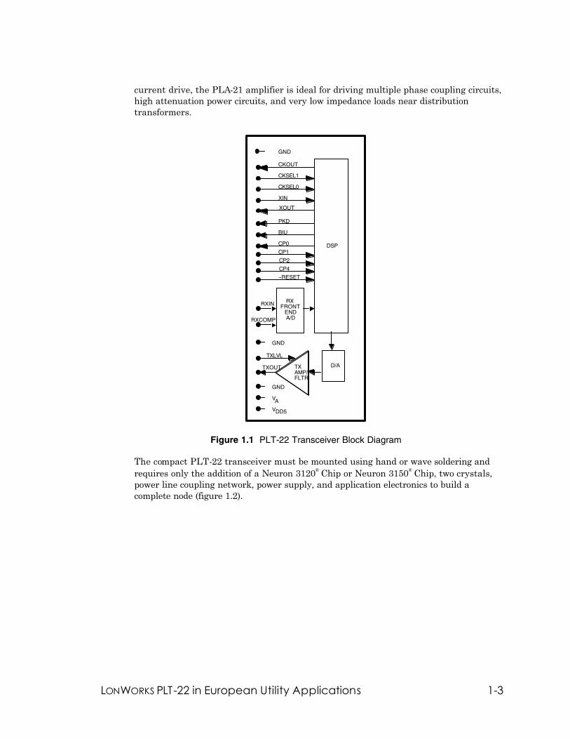
DSP
D/A
CP0
CP1
CP2
CP4
~RESET
BIU
CKOUT
GND
V
V
CKSEL0
CKSEL1
GND
GND
XOUT
XIN
RX FRONT
END A/D
RXIN
RXCOMP
TX AMP/FLTR
TXOUT
TXLVL
PKD
A
DD5
Figure 1.1 PLT-22 Transceiver Block Diagram
The compact PLT-22 transceiver must be mounted using hand or wave soldering and requires only the addition of a Neuron 3120® Chip or Neuron 3150® Chip, two crystals, power line coupling network, power supply, and application electronics to build a complete node (figure 1.2).
1-4 Introduction
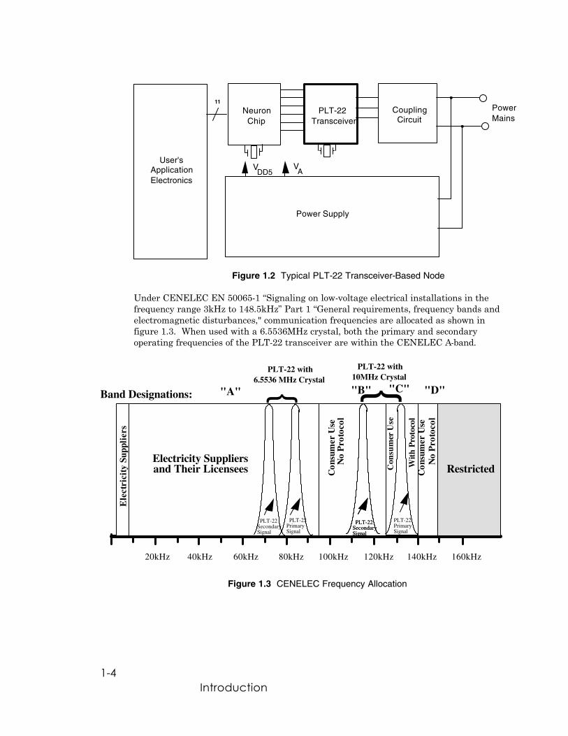
Neuron Chip
PLT-22 Transceiver
Coupling Circuit
Power Supply
User's Application Electronics
11
V
Power Mains
AVDD5
Figure 1.2 Typical PLT-22 Transceiver-Based Node
Under CENELEC EN 50065-1 “Signaling on low-voltage electrical installations in the frequency range 3kHz to 148.5kHz” Part 1 “General requirements, frequency bands and electromagnetic disturbances," communication frequencies are allocated as shown in figure 1.3. When used with a 6.5536MHz crystal, both the primary and secondary operating frequencies of the PLT-22 transceiver are within the CENELEC A-band.
20kHz 40kHz 60kHz 80kHz 100kHz 120kHz 140kHz 160kHz
Ele
ctri
city
Sup
plie
rs
Electricity Suppliers and Their Licensees C
onsu
mer
Use
Con
sum
er U
se
"A" "B" "C" "D"
RestrictedWit
h P
roto
col
No
Pro
toco
l
Band Designations:
PLT-22 Primary Signal
PLT-22 Secondary Signal
Con
sum
er U
seN
o P
roto
col
PLT-22 Secondary Signal
PLT-22 Secondary Signal
PLT-22 Primary Signal
PLT-22 with 6.5536 MHz Crystal PLT-22 with
10MHz Crystal
Figure 1.3 CENELEC Frequency Allocation

LONWORKS PLT-22 in European Utility Applications 1-5
Audience This document is intended for designers of products using the PLT-22 Power Line Transceiver in the CENELEC utility band (A-band).
Content This manual provides detailed operating instructions for the use of the PLT-22 transceiver in the CENELEC utility band.
Related Documentation The following documents are suggested reading:
PLT-22 Power Line Transceiver data sheet (003-0250-01)
PLCA-22 Power Line Communication Analyzer User’s Guide (078-0147-01)
LONWORKS Custom Node Development (005-0024-01)
LONMARK®Layers 1-6 Interoperability Guidelines (078-0014-01)
LONMARK Application Layer Interoperability Guidelines (078-0120-01)
Neuron Chip Data Book as published by Motorola and Toshiba

1-6 Introduction

LONWORKS PLT-22 in European Utility Applications 2-1
2
Using the PLT-22 Transceiver
This chapter describes the electrical characteristics of the PLT-22 transceiver when used in the CENELEC utility band (A-band). Interface circuit requirements and application schematics for A-band use are also included.

2-2 Using the PLT -22 Transceiver
Mechanical Dimensions
Figure 2.1 presents the mechanical dimensions of the PLT-22 transceiver.
The PLT-22 is produced as an uncoated SIP (in contrast to the coated PLT-10A, and PLT-30 transceivers).
Figure 2.1 PLT-22 Transceiver Dimensions
Note: If a socket is required for prototype purposes, a Mill-Max #317-93-121-41-005 connector may be used. For more information, contact:
Mill-Max Manufacturing Corporation 190 Pine Hollow Road Oyster Bay, New York, 11771 Telephone: +1-516-922-6000 Fax: +1-516-922-9253 Internet: http://www.mill-max.com

LONWORKS PLT-22 in European Utility Applications 2-3
PLT-22 Transceiver Pinout
Table 2.1 lists the functions of the PLT-22 transceiver pins.
Table 2.1 PLT-22 Transceiver Pinout
Pin # Pin Name Function 1 RXCOMP Connection to receive compensation component 2 RXIN Receive signal input from line coupling circuit 3 GND Ground 4 CP4 Frame clock synchronization from Neuron Chip (FCLK) 5 CP2 Bit clock synchronization from Neuron Chip (BCLK) 6 CP1 Transmit data and configuration from Neuron Chip (TXD) 7 CP0 Receive data and status to Neuron Chip (RXD) 8 GND Ground 9 VDD5 +5VDC power supply input
10 CKOUT Buffered CMOS clock output: 6.5536 MHz ÷ 1, 2, 4 or 8 11 CKSEL0 Selects frequency of CKOUT—see table 2.4 12 CKSEL1/TXON Selects frequency of CKOUT—see table 2.4 / TXON (supports
PLA-21 Power Line Amplifier) 13 ~RESET Reset input from Neuron Chip 14 BIU CENELEC Band-In-Use indication output 15 PKD Packet detect indication output 16 TXOUT Transmit signal output to line coupling circuit 17 GND Ground 18 XIN 6.5536 MHz oscillator input 19 XOUT 6.5536 MHz oscillator output 20 VA Analog power supply input
21 TXLVL Transmit level selection input

2-4 Using the PLT -22 Transceiver
PLT-22 Transceiver Electrical Specifications
Table 2.2 lists the electrical specifications of the PLT-22 transceiver when used in the CENELEC A-band. All specifications apply over the full operating temperature and supply voltage ranges unless otherwise indicated.
Table 2.2 PLT-22 Transceiver Electrical Specifications
Parameter Min Typ Max Units
Operating temperature range1 -40 +85 ° C
VDD5 input supply voltage 4.75 5 5.25 Volts
VA input supply voltage
TXLVL = GND2 11.4 12.0 16 Volts
IDD5 input supply current (not including PKD and BIU LED Current)
receive 14 20 mA transmit 13 18 mA IA input supply current
receive 4 6 mA transmit 130 200 mA TXOUT signal level: TXLVL=GND, into 50• load 6.8 7.5 Volts p-p Output current limit 1.0 Amps p-p Output impedance, in-band (transmit) 0.9 1.1 Ohms Input impedance, in-band (receive) 500 Ohms PKD output source current @ VDD5-0.6 V 8 mA
BIU output source current @ VDD5-0.6 V 8 mA
Power management, lower threshold 7.2 7.9 8.5 Volts Power management, upper threshold 11.1 12.0 12.9 Volts
Notes:
1. Maximum operating temperature is a function of VA supply voltage and the maximum transmission duty cycle for the node. A maximum operating temperature of 85°C is specified for a VA supply ≤12.6V and a maximum transmit duty cycle of 65%, which is the maximum achievable with LONMARK interoperable transceiver parameters and messages of ≤34 Bytes. For other cases see figure 2.2.
2. The VA supply must not drop below 11.4V under conditions of typical line voltage, room temperature, and typical current drain (including the PLT-22 transceiver’s typical IA transmit current of 130mA). This condition ensures adequate transmit amplifier

LONWORKS PLT-22 in European Utility Applications 2-5
headroom to drive the full 7Vp-p signal onto typical lines. Under worst case conditions, the minimum VA supply voltage may be relaxed if the following additional condition is met. With worst case power supply loading (including PLT-22 IA = 200mA), worst case component tolerances, worst case line voltage, and worst case temperature, VA must remain greater than or equal to 9.0V. This condition ensures adequate transmit amplifier headroom when driving low impedance power lines. When using an energy storage type power supply refer to Chapter 5 for additional timing requirements on the above conditions.
50% 60% 70% 80% 90%40% 100%30%20%10%
85
80
75
70
65
60
55
50
45
40
30
35
25
VA Max =12.6V
VA Max =16V
Transmit Duty Cycle
Max
imum
O
pera
ting
Tem
pera
ture
(°C
)
Maximum possible transmit duty cycle using LONMARK interoperable transceiver parameters and messages Š34 bytes
Figure 2.2 PLT-22 Transceiver Maximum Operating Temperature vs. Transmit Duty Cycle
2-6 Using the PLT -22 Transceiver
External Components
Crystal The PLT-22 transceiver requires the connection of an external 6.5536MHz crystal for A-band operation. The crystal connects directly to two pins of the PLT-22 transceiver, with no other oscillator components being required external to the transceiver. The crystal should be mounted as close as possible to the transceiver to minimize parasitic effects. The traces connecting the crystal to the transceiver preferably should be less than 10mm (0.4") in length, and under no circumstances can they exceed 20mm (0.8") in length.
In addition to the nominal frequency specification of 6.5536MHz, the crystal should be a parallel resonant type with a load rating of 16 pF (series resonant crystals should not be used). The frequency accuracy of the oscillator must be held to ±200 ppm over the full temperature range of operation.
While the PLT-22 transceiver design is centered around the use of a crystal whose load capacitance rating is 16pF, it is possible to recenter the design for a crystal whose load capacitance rating is higher than 16pF. The PLT-22 transceiver effectively contains two 32pF capacitors, one from XIN to ground and one from XOUT to ground. Note that the series combination of the two capacitors equals the load capacitance of the recommended crystal. Recentering the design for the use of a crystal with a higher load capacitance specification requires the addition of two external capacitors whose series equivalent capacitance is equal to the load capacitance specification of the crystal less 16pF. For instance, to use a crystal with a load capacitance specification of 20pF, the operating frequency can be centered by adding two 8.2pF capacitors, one from XIN to ground and one from XOUT to ground.
If a 6.5536MHz±200ppm 0-5V clock signal is already available as part of the node hardware then it may be used as a clock source for the PLT-22 transceiver by connecting it to Pin 18 (XIN) of the transceiver. In this instance Pin 19 (XOUT) of the PLT-22 should be left unconnected. With this option, appropriate high speed clock distribution techniques must be strictly followed in order to ensure that a clean clock signal is present at the XIN pin of the PLT-22 transceiver.
Oscillator frequency accuracy should be checked during the design verification phase of every PLT-22 based product. Frequency accuracy should be measured by using a frequency counter connected to the CKOUT pin to compare the frequency of that pin to 6.5536MHz divided by 8. Be sure that no instruments or extra cabling are connected to either the XIN or XOUT pins of the PLT-22 since even 2pF of extra load on either pin will significantly change the oscillator frequency.
Power Supply Bypassing and Grounding The PLT-22 transceiver requires the connection of external bypass capacitors. The bypass capacitors should be placed as close as possible to the PLT-22 transceiver, and low-impedance ground and supply traces should be used between the PLT-22 transceiver and the bypass capacitors. In addition to the bypass capacitors specified for the Neuron
LONWORKS PLT-22 in European Utility Applications 2-7
Chip (see Neuron Chip Data Book 2,3,16), the recommended values of the VDD5 and VA bypass capacitors are, as follows:
VDD5: None required if the VDD5 supply at the PLT-22 transceiver pin 9 meets the noise masks described in Chapter 5. It is recommended that PCB designs initially incorporate a 10µF 10V tantalum capacitor and a 0.1µF ceramic capacitor on the VDD5 suppy. These capacitors can be eliminated if the design meets the noise masks in Chapter 5 and passes the receive performance tests described in Chapter 7 without the capacitors installed.
VA: 120µF (minimum) 16V, low-ESR (<0.3Ω @ 100kHz), high-frequency aluminum electrolytic capacitor. Low ESR is required in order to minimize VA ripple voltage when the transceiver drives low impedance loads, drawing several hundred milli-Amperes of peak-to-peak ripple current. Note that the VA bypass capacitor is an integral part of the mains surge protection circuitry described in Chapter 4. In particular, the coupling circuits of Chapter 4 require the use of an aluminum electrolytic type capacitor with a voltage rating of 16V. Higher or lower voltage ratings will likely result in surge immunity which is significantly below the verified levels documented in Chapter 4.
The PLT-22 transceiver provides three ground pins. For proper operation, all three pins must be connected to ground with low-impedance traces, or to a ground plane between the transceiver and the Neuron Chip.
Band-In-Use (BIU) and Packet Detect (PKD) LED Connections The PLT-22 transceiver supplies two output signals, PKD and BIU, that are intended to drive low-current light-emitting diodes (LEDs). Both signals are active-high and must be connected to separate LEDs, with series current-limiting resistors added between the LEDs and ground.
The Band-In-Use function is defined for purposes in the CENELEC C-band and is not required for A-Band operation. When the PLT-22 transceiver is programmed with proper A-band transceiver parameters, as described in Chapter 3, an active BIU signal does not prevent the PLT-22 transceiver from transmitting. Nevertheless, the BIU signal can still be used to indicate when there is a signal in the transceiver’s primary carrier frequency range of approximately 85dBµV or larger.
The PKD signal is active whenever a valid LonTalk® packet is being received by the PLT-22 transceiver. The receive sensitivity of the transceiver is considerably greater than that of the BIU indicator. The PKD signal will go active when the PLT-22 transceiver receives packets whose signal level is as small as 40dBµVrms. Thus it is not uncommon for the PKD indicator to signal that a packet is present without the BIU indicator turning on; this occurs in cases where the received packet signal strength is less than the BIU threshold.
Both the BIU and PKD signals are driven directly by the PLT-22 transceiver’s DSP processor. ESD protection diodes should be connected to these pins in applications where the BIU and PKD signals drive LEDs that could be subject to ESD exceeding 2kV. In applications where the LEDs are surrounded by a metallic ground plane, such

2-8 Using the PLT -22 Transceiver
as a hole in a grounded metal enclosure, the ESD diodes may not be necessary. However, if a plastic or metal enclosure without a good ground connection is used, then ESD diodes are needed to prevent damage to the PLT-22 transceiver. ESD protection diodes include industry part types 1N4148 (thru-hole) and BAV99 (SMT).
Neuron Chip Connections The link between the Neuron Chip and the PLT-22 transceiver makes use of the Neuron Chip's special-purpose mode interface. This interface requires that the CP and ~RESET lines of the two devices be interconnected as shown in table 2.3.
Table 2.3 Neuron Chip and PLT-22 Transceiver Interconnections
Neuron Chip Pin PLT-22 Pin
CP0 7
CP1 6
CP2 5
CP3 Do not connect
CP4 4
~Reset 13
CLK1 10
The Neuron Chip and PLT-22 transceiver should be placed adjacent to one another on the same printed circuit board. The length of the ~RESET and CP lines should be kept to an absolute minimum and in no case should exceed 50mm (2"). In addition, the ground traces and VDD5 trace between the PLT-22 transceiver and the Neuron Chip should have impedances as low as possible.
When the PLT-22 transceiver is operated in the A-band (with a 6.5536MHz crystal), a second and separate crystal is required to operate the Neuron Chip at one of its standard operating frequencies of 2.5MHz, 5MHz, or 10MHz. Note that the minimum Neuron Chip clock frequency required for use with the PLT-22 transceiver operating in the A-band is 2.5MHz.
For A-band operation the CKOUT pin of the PLT-22 transceiver should be left unconnected. The CKSEL1 pin of the transceiver should be left open, unless it is used to drive the TXON pin of a PLA-21 Power Line Amplifier. The CKSEL1/TXON pin must never be connected directly to a supply rail. The CKSEL1/TXON pin will draw large currents and potentially damage the PLT-22 transceiver if it is connected directly to a supply rail. The CKSEL0 pin of the transceiver should be connected to ground and should not be left open.
The PLT-22 transceiver ~RESET pin is designed to connect directly to the Neuron Chip ~RESET pin. The Neuron Chip Data Book 2,3,16 provides information on the Neuron Chip’s external reset circuitry. Depending on the particular Neuron Chip version used, a Low Voltage Indicator (LVI) circuit such as the Motorola
LONWORKS PLT-22 in European Utility Applications 2-9
MC33064 or Dallas 1233 may be necessary to supply a reset signal to both the Neuron Chip and the PLT-22 transceiver. All of the application circuits shown in this documentation include an LVI chip. Consult your Neuron Chip manufacturer for the latest reset circuit requirements. Whether an LVI chip or a simpler discrete circuit is required, the ~RESET pin of the PLT-22 should always be tied directly to the ~RESET pin of the Neuron Chip. To minimize the effect of ESD discharges on the Neuron Chip ~RESET pin, use two external 56pF ceramic capacitors, one tied between ~RESET and VDD5, the other between ~RESET and GND. The capacitors should be placed as close as possible to the Neuron Chip ~RESET pin. Note that the PLT-22 transceiver already incorporates two 56pF capacitors on the ~RESET line internal to the transceiver. These internal capacitors should be taken into account when calculating the total allowable capacitive load on the Neuron Chip ~RESET pin, as specified in the Neuron Chip Data Book2,3,16.
Transmit Output Level
The TXLVL input pin on the PLT-22 transceiver determines the output voltage of the transmit signal. For A-band operation of the PLT-22 transceiver, the TXLVL pin should be grounded so that the transceiver will transmit a 7Vp-p signal. This level satisfies CENELEC 50065-1 signal level requirements for operation in the A-band. Since the 20dB bandwidth of the PLT-22 A-band signal is >5kHz, CENELEC regulations require that the overall signal level not exceed 134dBµV and that the spectrum of the signal not exceed 120dBµV within a 200 Hz bandwidth. When used with a recommended coupling circuit from Chapter 4, the overall level of the PLT-22 transceiver operated at 7Vp-p is 121dBµV and its level with a 200 Hz bandwidth filter is 117dBµV.
TXON Output Signal
The PLT-22 transceiver provides an output signal suitable for controlling a PLA-21 Power Line Amplifier via the CKSEL1/TXON pin. The CKSEL1/TXON pin functions as an input during the period in which the ~RESET pin of the PLT-22 transceiver is held active (low). After RESET becomes inactive (high) CKSEL1/TXON changes to an output (CKSEL0 remains an input, but its state is ignored). The output, called TXON, is a buffered version of the internal signal used to control the transceiver's output amplifier. The TXON signal output is active high when the PLT-22 transceiver transmits packets.
The TXON signal is typically used to provide tri-state control of an external booster amplifier, such as the PLA-21 Power Line Amplifier model 53001-01. For more details see the PLA-21 Power Line Amplifier Specification and User's Guide.

2-10 Using the PLT -22 Transceiver
LONWORKS PLT-22 in European Utility Applications 2-11

2-12 Using the PLT -22 Transceiver

LONWORKS PLT-22 in European Utility Applications 3-1
3
PLT-22 Transceiver Programming
Certain parameters of the PLT-22 transceiver are programmed by the user. This chapter presents a list of these parameters and their values, plus a description of how they are programmed via the LonBuilder® Developer’s Workbench and the NodeBuilder™ Development Tool.
3-2 PLT-22 Transceiver Programming
Dual Carrier Frequency Mode Each PLT-22 transceiver incorporates a new dual carrier frequency capability which allows it to communicate with other PLT-22-based nodes, even if noise is blocking its primary communication frequency range. If impairments prevent communication in this range, a PLT-22-based node can automatically switch to a secondary carrier frequency to complete a transaction with other PLT-22-based nodes.
With dual carrier frequency mode, the last two retries of acknowledged service messages are sent using the secondary carrier frequency. Thus when acknowledged service is used with three retries (four total tries), the first two tries are sent using the 86kHz primary carrier frequency. If the last two tries are needed to complete the transaction, they are sent (and acknowledged) using the 75kHz secondary carrier frequency. A minimum of two retries must be used if the PLT-22 transceiver is to be able to use both carrier frequency choices. For optimum reliability and efficiency, Echelon recommends the use of three retries when using acknowledged service messaging with the PLT-22 transceiver.
When unacknowledged repeat message service is used, the PLT-22 transceiver leverages the reliability of both carrier frequencies by alternating between them. In this case an unacknowledged repeat message with three repeats results in the first and third packets being sent using the 86kHz primary carrier frequency, while the second and fourth packets are sent using the 75kHz secondary carrier frequency. A minimum of one repeat must be used for the PLT-22 transceiver to use both carrier frequency choices. For improved reliabiliy, three repeats are recommended.
CENELEC Access Protocol CENELEC regulations do not specify an access protocol for use in the CENELEC A-band. When programmed with the A-band transceiver parameters described later in this chapter, the PLT-22 transceiver’s internal CENELEC access protocol is disabled. With this selection, an active Band-In-Use signal will not prevent a PLT-22 from transmitting.
Power Management The PLT-22 transceiver incorporates a power management feature that supports the design of very low cost power supplies in low cost consumer applications. This class of consumer applications generally has low transmit duty cycle operation requirements. These low cost power supplies take advantage of a number of PLT-22 features: the low receive current requirements of the PLT-22 transceiver; the 9:1 difference between the PLT-22 transceiver transmit and receive mode currents and the wide VA operating voltage of the PLT-22 transceiver.
A low transmit duty cycle implies that the device transmits packets infrequently, e.g., the product waits for a minimum of 10 packet times between transmitting each packet - a 10% transmit duty cycle. A power supply design that takes advantage of this duty cycle can store energy on a capacitor during the relatively long period between transmissions, when the PLT-22 transceiver draws minimal current, and then consume the stored energy to transmit a packet. This type of power supply, referred to as an
LONWORKS PLT-22 in European Utility Applications 3-3
“energy storage power supply,” stores energy by charging an energy storage capacitor to a relatively high voltage (e.g., 15V) while in receive mode. The voltage on the capacitor then falls or "droops" toward a lower limit (e.g., 9.0V) while transmitting. The energy storage capacitor is then slowly recharged to the higher voltage during the relatively long time between transmissions. Traditionally, the proper design of such a power supply required knowledge of the maximum transmit duty cycle to be supported, and an implementation that accounted for all worst case operating conditions (temperature, line voltage, component variation and transmitter loading).
The cost of such a power supply can be significantly reduced if, instead of designing the supply for the maximum possible transmit duty cycle and for the worst case environmental conditions, the supply can be designed for typical operating conditions. However, designing for typical operating conditions implies that a mechanism exists to "manage" the worst case operating conditions such that reliable operation is assured. This management feature must also address products whose operating conditions (especially transmit duty cycle) are not defined prior to use in a network, but rather are controlled by application programs loaded after installation.
The PLT-22 power management feature implements the needed management functionality by intelligently monitoring the energy storage power supply. Should the node attempt to transmit too frequently, the power management feature enforces a limit on the transmit duty cycle by preventing the Neuron Chip from transmitting until the node's power supply recovers to the point that sufficient energy is available to transmit a packet. Details of this feature and application examples are provided in Chapter 5.
When power management is enabled, the PLT-22 transceiver requires a VA power supply voltage of 12.9V before it will attempt to transmit a packet. Products with fixed VA power supplies lower than 12.9V should never be programmed to enable the power management feature as they may never be allowed to transmit. Likewise a node whose power supply relies on power management to operate correctly should never be programmed with the power management feature disabled.
The user can enable or disable power management at the time of channel definition by selecting a standard transceiver type with a "low" suffix. The only difference between a set of standard transceiver parameters with the "low" suffix and the corresponding set without the "low" suffix is that the power management feature is enabled with the "low" set and disabled with the set without the suffix.
Note that some installation tools load a device's communication parameters as part of the installation and replacement process and calculate those parameters based on the channel (rather than the particular device). Such tools can not be used for systems that contain a mixture of nodes with and without power management enabled on the same channel.
Tools based on the LONWORKS Network Services (LNS) architecture, such as LonMaker for Windows Integration Tool, correctly support all configurations of PLT-22 nodes with or without power management. For a tool not based on LNS, contact your tool vendor to determine if it can support a mixture of power management and non-power management nodes on the same channel.
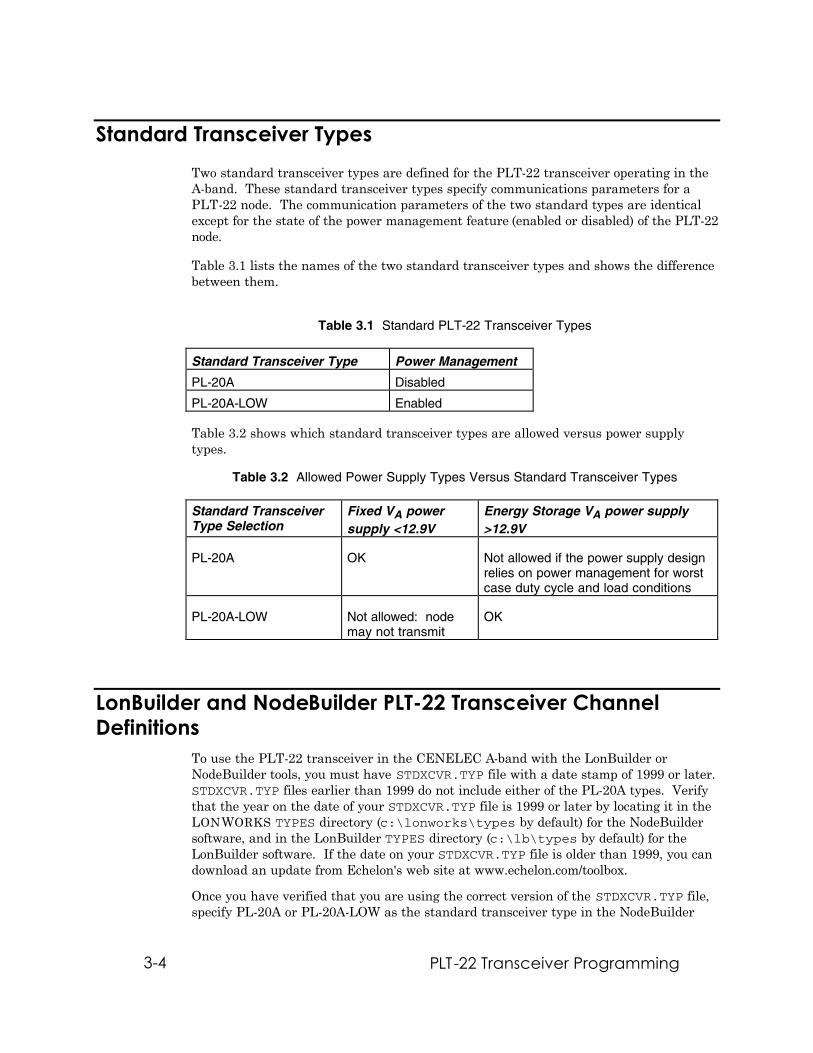
3-4
Standard Transceiver Types
Two standard transceiver types are defined for the PLT-22 transceiver operating in the A-band. These standard transceiver types specify communications parameters for a PLT-22 node. The communication parameters of the two standard types are identical except for the state of the power management feature (enabled or disabled) of the PLT-22 node.
Table 3.1 lists the names of the two standard transceiver types and shows the difference between them.
Table 3.1 Standard PLT-22 Transceiver Types
Standard Transceiver Type Power Management
PL-20A Disabled
PL-20A-LOW Enabled
Table 3.2 shows which standard transceiver types are allowed versus power supply types.
Table 3.2 Allowed Power Supply Types Versus Standard Transceiver Types
Standard Transceiver Type Selection
Fixed VA power supply <12.9V
Energy Storage VA power supply >12.9V
PL-20A OK Not allowed if the power supply design relies on power management for worst case duty cycle and load conditions
PL-20A-LOW Not allowed: node may not transmit
OK
LonBuilder and NodeBuilder PLT-22 Transceiver Channel Definitions
To use the PLT-22 transceiver in the CENELEC A-band with the LonBuilder or NodeBuilder tools, you must have STDXCVR.TYP file with a date stamp of 1999 or later. STDXCVR.TYP files earlier than 1999 do not include either of the PL-20A types. Verify that the year on the date of your STDXCVR.TYP file is 1999 or later by locating it in the LONWORKS TYPES directory (c:\lonworks\types by default) for the NodeBuilder software, and in the LonBuilder TYPES directory (c:\lb\types by default) for the LonBuilder software. If the date on your STDXCVR.TYP file is older than 1999, you can download an update from Echelon's web site at www.echelon.com/toolbox.
Once you have verified that you are using the correct version of the STDXCVR.TYP file, specify PL-20A or PL-20A-LOW as the standard transceiver type in the NodeBuilder
PLT-22 Transceiver Programming

LONWORKS PLT-22 in European Utility Applications 3-5
Device Template, as shown in figure 3.1, or the LonBuilder Channel Create window. Select “Yes” for the “Enforce Standard Type” field.
Figure 3.1 NodeBuilder Device Template Window
Table 3.3 shows the channel definition parameters for the PLT-22 transceiver. If you do not have access to an updated STDXCVR.TYP file, these channel definition parameters may be entered in the Channel Modify screen and sub-screens to create a standard PLT-22 transceiver definition equivalent to the PL-20A or PL-20A-LOW parameters
Table 3.3 Channel Definition Parameters for the PLT-22 Transceiver
Parameter Value Channel Modify Screen Std Xcvr Type Custom Comm Mode Special Purpose Comm Rate 1.25Mbps Number of Priorities 8 Min Clock Rate 2.5MHz Avg Pkt Size 15 bytes Osc Accuracy 200ppm Osc Wakeup 0 µsec

3-6
Table 3.3 Channel Definition Parameters for the PLT-22 Transceiver (continued)
Comm Mode Specific Parameters Channel Bit Rate 2613 bps Alternate Bit Rate 2613 bps Wakeup Pin Dir Output Xcvr Controls Preamble? Yes General Purpose Data (power management disabled) General Purpose Data (power management enabled)
0E 01 00 10 00 00 00 0E 01 00 12 00 00 00
Allow Node Override? PL-20A, PL-20A-LOW
YES
Layer 1 Time Factors Rcv Start Delay 6.8 bits Rcv End Delay 1.6 bits Indeterm Time 0.0 bits Min Interpacket 17.5 bits Preamble Len 33.5 bits Use Raw Data? No
The standard transceiver definitions in table 3.1 were chosen as the best balance between flexibility in network design and network throughput. Flexibility is provided by the selection of 8 priority slots on the channel and a minimum input clock of 2.5MHz (a Neuron Chip input clock frequency as low as 2.5MHz may be chosen in order to reduce node power consumption). These parameters support a packet rate of 6 packets/sec with 80% throughput, 4% collisions, and 11 byte packets.
PLT-22 Transceiver Programming
LONWORKS PLT-22 in European Utility Applications 4-1
4
Coupling Circuits
This chapter includes a technical discussion about the means by which communication signals are coupled to power mains. Coupling circuit designs, including schematics and electrical safety issues, are included.
4-2 Coupling Circuits
Power Line Communications
The PLT-22 transceiver employs sophisticated digital signal processing techniques, a transmit power amplifier with a very low output impedance, and a very wide (>70dB) dynamic range receiver to overcome the signal attenuation and noise inherent in power mains communication. Maintaining the full communication capability of the PLT-22 transceiver requires careful selection and implementation of the mains coupling circuitry external to the PLT-22 transceiver. This section gives an overview of the sources of signal attenuation as a basis for understanding choices in selecting and implementing mains coupling circuits. Attenuation is the difference between the signal level at the output of the power line transmitter and the level of that same signal at the input of the intended receiver. While attenuation is technically defined as the ratio of power levels, it is referred to in this document as the ratio of the transmitted signal voltage (unloaded) to the voltage of that same signal at the receiver input. A voltage ratio is more convenient to measure since power measurements require knowledge of the circuit impedance which, in the case of the power mains, varies with both location and time. In power mains communications the attenuation of transmitted signals spans a wide range and is most conveniently denoted in decibels (dB), where voltage attenuation is defined in dB as 20log10 (Vtransmit/Vreceive). Thus 20dB of attenuation means that the signal was reduced by a factor of 10 by the time it arrived at the receiver, 40dB of attenuation corresponds to a factor of 100, 60dB a factor of 1000, and so on. A PLT-22 transceiver operating in the A-band is capable of reliably communicating on a low-noise line when the transmit signal is attenuated by as much as 77dB (a factor of 7,000). Thus a signal transmitted at 7Vp-p (2.5Vrms) may be received when reduced to less than 1mVp-p (350µVrms). To better understand the sources of attenuation in a power mains network, it is helpful to look at a simplified model of a power distribution network. This example is based on an installation having one power distribution transformer and three phases of mains power. While many applications for power line communication employ different topologies, this example illustrates some of the key issues affecting the successful application of the PLT-22 transceiver. Figure 4.1 depicts the path that a power line communication signal might traverse, starting from a utility distribution transformer and passing through the distribution wiring to the electricity meter on a particular home. Each home in the power network may power devices that generate noise and load the transmitted signal.

LONWORKS PLT-22 in European Utility Applications 4-3
TX
RX
Distributor Transformer
TX
RX
L1L2
L3
Figure 4.1 Power Distribution Model
Attenuation is most easily understood in terms of a voltage-divider circuit formed by the output impedance of the transmitter, the impedance of the various mains distribution branches, and any loads present. At A-band communication frequencies of the PLT-22 transceiver (70kHz to 95kHz), the significant impedances are due to the series inductance of the mains wiring itself, and capacitive and resistive loads between line and neutral. Another source of attenuation occurs in the example of figure 4.1 when the communicating devices are not all connected to the same AC mains phase. Mutual inductance and parasitic capacitance provide partial (but imperfect) coupling between circuit phases. If these distributed impedances are lumped together and treated as if a single frequency is being transmitted, the simple model shown in figure 4.2 results.
Transmitter
Wiring Phase-to-Phase
Receiver
Power Line Signal Return Path
TransmitterZ o Z Z WiringZ
LoadZ LoadZ LoadZ ReceiverZ i
Figure 4.2 Power Mains Attenuation Model

4-4 Coupling Circuits
This model illustrates that minimizing the series impedances and maximizing the line-to-return path impedances reduces the attenuation of the transmitted signal.
Coupling Techniques
Power Line Coupling Basics
Injecting a communication signal into a power mains circuit is normally accomplished by capacitively coupling a transceiver's output to the power mains. In addition to the coupling capacitor, an inductor or transformer is generally present. The coupling capacitor and the inductor or transformer together act as a high-pass filter when receiving the communications signal. The high-pass filter attenuates the large AC mains signal (at 50Hz), while passing the transceiver's communication signal. Figure 4.3 below shows a basic mains coupling circuit. The value of the capacitor is chosen to be large enough so that its impedance at the communication frequencies is low, yet small enough that its impedance at the mains power frequency (50Hz) is high. The impedance of the capacitor can be considered as part of the transmitter's output impedance (ZoTransmitter ) shown in figure 4.2. Keeping the impedance of the coupling capacitor low minimizes the signal injection loss caused by the voltage divider formed between the output impedance of the amplifier and the mains loading (ZLoad).
The value of the inductor is chosen to have a relatively high impedance at the PLT-22 transceiver's communication frequencies. The inductor impedance can be considered part of the receiver input impedance (Zi Receiver) shown in figure 4.2. Keeping the inductor impedance high helps minimize any signal loss at the receiver due to the voltage divider formed by the wiring impedance and the receiver input impedance.
PL Transmitter
PL Receiver
Line
Neutral
Figure 4.3 Basic Mains Coupling Circuit

LONWORKS PLT-22 in European Utility Applications 4-5
In the following section the simple circuit shown in figure 4.3 is expanded to make it practical in real applications. At the end of this chapter, recommended coupling circuit schematics and component specifications are provided.
Power Line Coupling Details The coupling circuit shown in figures 4.3 requires the addition of a small number of components to make it practical. Figure 4.4 shows the addition of an AC coupling capacitor (C2) to prevent the inductor from shorting the transmit amplifier's DC bias voltage.
Transmit Amp
Receive Front End
PLT-22
C1C2
L1
Figure 4.4 Simplified Coupling Circuit with Blocking Capacitor
Given the attenuation model presented earlier in figure 4.2, one critical design constraint is that the series combination of C1 and C2 must have a low impedance at the PLT-22 transceiver's communication frequencies. The impedance of these capacitors, along with the PLT-22 transceiver's transmit output impedance, corresponds to “Zo Transmitter” in figure 4.2. Since the equivalent load impedance of the power line may in some cases be as low as 1-2 Ohms, and since the output impedance of the PLT-22 transceiver is less than 1 Ohm, the impedance of these capacitors should be on the order of 1 Ohm so that they do not add significantly to “Zo Transmitter”. While the values of C1 and C2 could be set high enough to meet this goal, doing so would significantly increase the cost of the high-voltage capacitor C1. Since C2 is connected only to low voltage, and thus is lower cost for a given value, its value can be set higher relative to the value of the high-voltage capacitor C1. A simple, cost-effective solution is obtained when an inexpensive inductor, L2, is added as shown in figure 4.5 below. This inductor forms a series-resonant circuit with C1 and C2,

4-6 Coupling Circuits
and its value can therefore be chosen to optimize coupling at the PLT-22 transceiver's communication frequencies while minimizing the cost of C1 and C2.
Transmit Amp
Receive Front End
PLT-22
C1C2
L1
L2
Figure 4.5 Simplified Coupling Circuit with Resonant Inductor
An important design constraint on L2 is that its DC resistance be kept very low since it is in the transmit signal path and effectively part of the transmitter's output impedance. Low-cost inductors with DC resistance on the order of 0.2 Ohms are widely available.
Capacitors C1 and C2 should be of metalized polyester construction in order to minimize equivalent series resistance and provide adequate surge immunity.
It is critical that no additional series impedance be added in the signal path between the TXOUT pin of the PLT-22 transceiver and the power mains (or in the return path from the power mains to the ground pins of the PLT-22) unless verified to be significantly less than 1 Ohm near 85kHz. If, for example, a ferrite bead with an impedance of 9 Ohms at 85kHz were added then the signal injected into a 1 Ohm power line would be reduced by a factor of 10. Under typical conditions the end product would still function, however, communication margin and reliability over a full range of power line environments would be severely compromised. For the same reason, the impedance of series circuit protection elements must also be kept very low. Low current fuses (<2A), protection devices that can be reset, and ferrite beads generally add unacceptable series impedance to the signal path.

LONWORKS PLT-22 in European Utility Applications 4-7
Figure 4.6 shows additions to the coupling circuit, which are required to make it fully functional. The first is a 1.5mH inductor, L3, connected to the PLT-22 transceiver receive filtering circuitry. The DC resistance of L3 can be up to 60 Ohms. The second is the LCR trap circuit consisting of C4, L4, and R2. This circuit is added to attenuate out-of-band spurious emissions and comply with CENELEC conducted emission regulations. The third is a diode, D1, connected from the transmitter to the amplifier supply voltage (VA) to protect the inputs of the PLT-22 transceiver from large (>15V) transients. This diode works in conjunction with a diode internal to the PLT-22 transceiver that connects from the transmitter output to ground. Bypass capacitor C3 also has been added to emphasize the fact that it is an integral part of the coupling circuit. One of the functions of this capacitor is to protect the VA supply line from excessive overshoot when positive going line surges discharge through diode D1. The last addition is an optional circuit that improves performance in environments where large (>20V) impulses may be present from devices such as SCR-controlled loads. This circuit consists of an LCR series network that acts as a notch filter whose center frequency is at the characteristic “ringing” frequency of the coupling circuit. This optional circuit should be included on nodes which will be operated in environments where large (>20V) implusive noise is expected on each ac mains half cycle (i.e., at a 100 Hz rate).
Transmit Amp
Receive Front End
PLT-22
TXOUT
RXIN
RXCOMP
V
Optional
circuit
D1
C2
L3
C3+
A
L2B Line
Neutral
C1
L1
L2A
C4
L4
R2
C5
L5
R5
Figure 4.6 Functional Line-to-Neutral Coupling Circuit

4-8 Coupling Circuits
In instances where large ambient fields may be present (such as from switched mode power supply open frame magnetic elements), it is possible that one or more of the PLT-22 coupling circuit inductors may pick up these stray fields and conduct them onto the power mains. Depending on the frequency and amplitude of these fields they could result in failure to meet CENELEC conducted emission regulations.
If noise from parasitic coupling is suspected, it can be confirmed by inserting a 10cm (4”) twisted wire pair in series with one of the inductors in question. If the conducted noise spectrum varies by more than a few dB when this inductor is moved closer to, and farther from, other components, then parasitic coupling may be the source of the problem.
If stray coupling is a problem, regulations can usually be met by adjusting the location or orientation of the radiating device relative to the coupling circuit inductors. Alternately, shielded or toroidal inductors may be used to reduce coupling as long as all electrical parameters specified in the example coupling circuit tables given later in this chapter are met. If, however, a toroidal or shielded inductor is used in place of L2A or L2B, then the selected part must handle the maximum 1App output current of the PLT-22 transceiver without approaching saturation. If either L2A or L2B even approaches saturation they can add harmonics of the PLT-22 transmit signal which may result in failure to meet CENELEC emission regulations (in this instance, due to inductor distortion instead of a stray pickup). For this reason, a shielded or toroidal inductor used for L2A or L2B may need to have DC current rating two or three times higher than listed in the example circuits given later in this chapter. Note that the recommended open frame axial inductors do not need this extra operating margin due to the linearity provided by its magnetic path being partly in air.
Safety Issues
This guide is intended only as an introduction to some of the safety issues associated with designing circuits using the PLT-22 transceiver. This document is not a primer on electrical safety or electrical codes, and it is the responsibility of the user to familiarize himself or herself with any applicable safety rules or regulations. A review of all designs by competent safety consultants and the pertinent regulatory or safety agencies is strongly recommended.
Safety Isolation Considerations Many products include an isolation barrier in the form of an insulated enclosure between a user and any hazardous conductors. A typical product of this type is a light switch in which the PLT-22 transceiver and all of the associated electrical components are contained inside the switch enclosure. The type of coupling circuit that can be used in these applications is called a non-isolated coupling circuit. A non-isolated coupling circuit generally requires lower cost components, making it especially desirable for use in price-sensitive consumer products and wiring devices. All of the coupling circuit examples that have been shown so far are of the non-isolated type.
Some products cannot practically incorporate an enclosed isolation barrier and an alternate method of safety isolation must then be provided. For example, a circuit board that uses a PLT-22 transceiver, a non-isolated line-to-neutral coupling circuit, and a Neuron Chip
LONWORKS PLT-22 in European Utility Applications 4-9
whose I/O pins are user-accessible presents a potential electrical shock hazard. Since the mains neutral lead is connected directly to the circuit board common, the user could be exposed to a hazardous voltage at the I/O connector, especially if the line and neutral connections are accidentally reversed. Additional circuitry is needed in such a product to provide a safety isolation barrier between the user-accessible I/O connector and the mains line and neutral conductors.
The most common solution is to provide isolation in the coupling circuit by modifying the simple coupling circuit described earlier. This style of coupling circuit is referred to as an isolated coupling circuit.
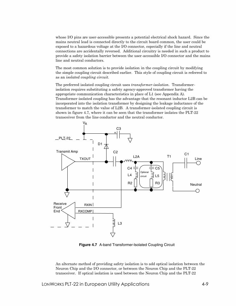
The preferred isolated coupling circuit uses transformer-isolation. Transformer-isolation requires substituting a safety agency-approved transformer having the appropriate communication characteristics in place of L1 (see Appendix A). Transformer-isolated coupling has the advantage that the resonant inductor L2B can be incorporated into the isolation transformer by designing the leakage inductance of the transformer to match the value of L2B. A transformer-isolated coupling circuit is shown in figure 4.7, where it can be seen that the transformer isolates the PLT-22 transceiver from the line conductor and the neutral conductor.
C3+
Transmit Amp
Receive Front End
PLT-22
TXOUT
RXIN
RXCOMP
V
Optional
circuit
D1
C2
Line
Neutral
T1C1
L3
A
L2A
C4
L4
R2
C5
L5
R3
Figure 4.7 A-band Transformer-Isolated Coupling Circuit
An alternate method of providing safety isolation is to add optical isolation between the Neuron Chip and the I/O connector, or between the Neuron Chip and the PLT-22 transceiver. If optical isolation is used between the Neuron Chip and the PLT-22

4-10 Coupling Circuits
transceiver, then a maximum of 150ns propagation delay may be added to the CP interface lines in either direction.
3 Phase AC Mains Circuits When communicating between PLT-22-based nodes located on different ac power phases, a significant portion of the overall attenuation between nodes is caused by loss in crossing phases (typically 10-20dB). Most of this loss can be avoided if one of the two nodes couples its signals to all three phases. In the example illustrated in figure 4.1 if all communications are to (and from) the node located at the central distribution transformer, then the use of a 3-phase coupling circuit in that node is recommended to maximize communication distance. Due to the fact that this central node must then drive the parallel combination of the impedance from all three phases, the use of a PLA-21 Power Line Amplifier is also recommended in that node to further extend operating distance.
Figure 4.8 illustrates how the PLA-21 Amplifier is connected between a PLT-22 transceiver and 3-phase coupling circuit. Refer to figure 4.12 and table 4.5 for detailed component values.
Transmit Amp
Receive Front End
PLT-22
TXOUT
RXIN
RXCOMP
L3
C2
Rgain
TXOUTTXIN
PLA-21
CLKSEL1/TXON TXON
GND
Line 1
Line 2
Line 3
Neutral
3-Phase Coupling Circuit
Figure 4.8 Connecting the PLA-21 Amplifier

LONWORKS PLT-22 in European Utility Applications 4-11
Capacitor Charge Storage
The coupling capacitors depicted in the earlier figures can retain substantial charge even after a PLT-22 transceiver-based device has been disconnected from the power mains. This can be of significant concern in applications where a line cord could be touched by a user after being disconnected from the power mains. To minimize potential shock hazard, coupling circuits should include a large value bleeder resistor to discharge the capacitors following disconnection from the mains. Even in applications where the connection to the mains is permanently wired, it is good practice to include the resistor to protect service personnel. The coupling circuit schematics in this document include appropriate bleeder resistors.
Line Surge Protection
Coupling circuits that connect the PLT-22 transceiver to the power mains also require the addition of component(s) to provide protection of the PLT-22 transceiver from the high-voltage surges that occur on all power distribution systems. Primarily lightning induced, these surges can present voltages of 6kV or greater at very high current levels for brief periods to the coupling circuits. The recommendations that follow are based on testing performed on a particular PCB layout. The efficacy of the surge protection implemented in each product containing the PLT-22 transceiver must always be verified empirically, since factors such as PCB layout and packaging can influence the results as much as the choice of protection components.
The level of surge protection required for a given product often depends on the installed location of the product to be protected. Devices connected to branch circuits within a building or home are typically subject to the lowest level of surge stress. Devices connected at, or close to, the power entry point of a building or home, e.g., electrical meters and main breaker panels, are subject to higher levels of surge stress. Devices connected to outdoor wiring are subjected to the highest surge stress of all.
Standard tests for surge immunity are defined in IEEE C62.41-199115and CEI/IEC 1000-4-514. Both documents classify levels of surge stress by the type of surge wave-form (either Ring wave or Combo wave), surge voltage, and surge current. In addition to describing standard test methods, both documents also suggest surge immunity levels for the device environments described above.

4-12 Coupling Circuits
Comparison of the two documents reveals that their recommended test procedures are identical, while the suggested immunity levels called out in IEEE C62.41-1991 substantially exceed the suggested immunity levels of CEI/IEC 1000-4-5. The more severe (and thus more conservative) immunity levels called out in IEEE C62.41-1991 were used in characterizing the recommended surge protection circuitry shown in the PLT-22 transceiver coupling circuit examples that follow.
The line-to-neutral coupling circuits documented later in this chapter have been demonstrated to meet the IEEE C62.41-1991 "high system exposure" levels with no damage for branch circuit applications, power entry applications, and outdoor wiring applications, up to the limits of the available test equipment.
Table 4.1 summarizes the surge immunity of the PLT-22 transceiver in conjunction with the specified line-to-neutral coupling circuits.
Table 4.1 Line-to-Neutral Coupling Circuit Surge Immunity Test Results
Ring Wave Test
(0.5µs-100kHz)
Combo Wave Test
(1.2/50µs-8/20µs)
Product Location
IEEE C62.41-1991 system exposure level
Surge level verified not to damage PLT-22
IEEE C62.41- 1991 system exposure level
Surge level verified not to damage PLT-22
Branch Circuit low -2kV @70A
med-4kV @130A
high-6kV @200A
6kV @200A
Not specified
6kV @500A
2kV @1,000A
Power Entry low -2kV @170A
med-4kV @330A
high-6kV @500A
6kV @500A
low -2kV @1,000A
med-4kV @2,000A
high-6kV @3,000A
6kV @3,000A
Outdoor Wiring
Not specified
6kV @500A
low -6kV @3,000A
med-10kV @5,000A
high-20kV @10,000A
6kV @3,000A (limited by test equipment)
LONWORKS PLT-22 in European Utility Applications 4-13
Fuse Selection Safety considerations may require a fuse in series with the mains connection. For an end product to continue to function (without user intervention) it is necessary that the selected fuse not open following a specified line surge. A minimum 6A time-lag (“slow blow”) rating has been shown to be necessary to avoid unintentional fusing action at “high system exposure” levels of IEEE C62.41-1991.
If a coupling circuit which incorporates varistor protection is selected, the varistor manufacturer’s recommendations for maximum fuse current should be followed. The vendor listed in the coupling circuits which follow suggests a maximum fuse rating of 6A for use with 7mm (1200A) varistors and a maximum rating of 18A for use with 14mm (4500A) varistors.
A 6A time-lag fuse is specified in all of the following coupling circuits since it satisfies all of the above criteria, as well as the critical requirement that it add very little resistance (<0.1 Ohms) to the transmit signal path. If a current rating greater than 6A is required by the application then either larger varistor (>7mm) or gas discharge tube protection is recommended.
Recommended Coupling Circuit Schematics This section provides schematics and component information for coupling the PLT-22 transceiver to the power mains. Three circuits are given, one each for isolated and non-isolated single phase coupling and one for 3-phase coupling. For each schematic, component specifications and suggested suppliers/part numbers are provided.
Vendor part number information is provided as a way to reduce component selection times, since the suggested parts have already been verified to meet all required specifications. Alternate component suppliers may be used provided that all specifications listed for each component are met.

4-14 Coupling Circuits
Example 1: A-Band, Line-to-Neutral (L-to-N), Non-Isolated Coupling Circuit
Figure 4.9 presents a schematic for a line-to-neutral, non-isolated mains coupling circuit. Table 4.3 lists component values and recommended suppliers/part numbers for coupling to the AC mains with a nominal line voltage in the range 100-240VAC.
Transmit Amp
Receive Front End
PLT-22
C2L2BTXOUT
RXIN
RXCOMP
L3
D1
C3VA
C1
L1
Line
Neutral
R1 PROTECT
F1
L5
C5
R3
See note below
L4
C4
R2
L2A
Inductors L1 and L3 should be spaced >1cm (0.4") apart to avoid undesirable parisitic coupling.
Note: This optional circuit should be added to nodes where >20V impulse noise is expected at ≥100Hz rate.
Figure 4.9 A-band, L-to-N, Non-Isolated Coupling Circuit Schematic

LONWORKS PLT-22 in European Utility Applications 4-15
Table 4.3 A-band, 100-240VAC, L-to-N, Non-Isolated Coupling Circuit Component Values
Comp Value Specifications Vendor / Part Number C1 0.10µF ±10%, •400VDC, metalized polyester(1) Matsushita Electric / ECQ-E4104KF
C2 0.82µF ±5%, •50VDC, metalized polyester Matsushita Electric / ECQ-V1H824JL C3 •120µF ±20%, 16VDC, aluminum electrolytic,
• 0.3• ESR @100kHz Matsushita Electric / ECA-1CFQ121
C4 4700PF ±5%, •50VDC AVX / SR205A472JAA C5 0.10µF ±5%, •50VDC AVX / SR205C104JAA D1 1A Reverse breakdown •50V, surge current •30A
for 8.3mS, reverse recovery •200nS 1N4935
F1 6A 250VAC, slow blow(2)
L1, L5 1.0mH ±10%, Imax•30mA, RDC•50• TAIYO YUDEN / LAL03NA102K
L3 1.5mH ±10%, Imax•30mA, RDC•60• RCD/ALO5 1500µH KT
L2A 27µH ±10%, Imax •1A, RDC•0.1• TAIYO YUDEN /LHL08TB270K(6) L2B 12µH ±10%, Imax •500mA, RDC•0.3• TAIYO YUDEN / LAL05TB120K
L4 33µH ±10%, Imax •50mA, RDC•5• TAIYO YUDEN / LAL03NA330K
R1 1M• ±5%, 1/4W, max working volt •360VDC(4)
R2 100• ±5%, •1/16W R3 82•-L5RDC
(3)
±5%, •1/16W
PROTECT 300VAC(240VDC) 300VAC(240VDC) 240VAC
For indoor branch circuits use 7mm varistor For power entry use 14mm varistor
For outdoor use AC gas discharge tube(5)
Matsushita Electric / ERZ-V07D471 Matsushita Electric / ERZ-V14D471 CPClare / AC240L
(1) In some applications an X2 safety rated capacitor may be required. Consult applicable safety standards.
(2) In some applications a fuse may not be required. Consult applicable safety standards.
(3) The value of R3 should be selected so that the series combination of the DC resistance of L5 and R3 is equal to 82•.
(4) The working voltage rating of R1 may be achieved by using two 470k• resistors in series, each with a working voltage rating of at least half of the value listed above.
(5) Install the gas discharge tube on the line side of F1 (if a fuse is used).
(6) If a toroidal inductor is required, Associated Components Technologies/T1-1A270K-S-1 is recommended.

4-16 Coupling Circuits
Example 2: A-band, Line-to-Neutral, Transformer-Isolated Coupling Circuit
Figure 4.10 presents a schematic for a line-to-neutral, transformer-isolated coupling circuit. Table 4.4 lists component values and recommended suppliers/part numbers for coupling to AC mains with a nominal line voltage in the range 100-240VAC.
Transmit Amp
Receive Front End
PLT-22
C2
TXOUT
RXIN
RXCOMP
L3
D1
C3VA
L5
C5
R3
C1T1 Line
Neutral
R1 PROTECT
F1
L4
C4
R2
See note below
L2A
Note: This optional circuit should be added to nodes where >20V impulse noise is expected at ≥100Hz rate.
Figure 4.10 A-band, L-to-N, Transformer-Isolated Coupling Circuit Schematic
For long haul operation (≥ 500m) on lightly loaded dedicated distribution lines communication distance can be maximized by installing a termination circuit at each end of the cable. A recommended termination circuit is shown in figure 4.11.
100•, ±10%, 1/2W, carbon composition0.1µF, ±10%, • 400VDC metalized polyester
Line
Neutral
Figure 4.11 Termination Circuit
LONWORKS PLT-22 in European Utility Applications 4-17
Table 4.4 A-band, 100-240VAC, L-to-N, Isolated Coupling Circuit Component Values
Comp Value Specifications Vendor / Part Number C1 0.10µF ±10%, ≥400VDC, metalized polyester(1) Matsushita Electric / ECQ-E4104KF
C2 0.82µF ±5%, ≥50VDC, metalized polyester Matsushita Electric / ECQ-V1H824JL C3 ≥120µF ±20%, 16VDC, aluminum electrolytic,
≥ 0.3Ω ESR @100kHz Matsushita Electric / ECA-1CFQ121
C4 4700PF ±5%, ≥50VDC AVX / SR205A472JAA C5 0.10µF ±5%, ≥50VDC AVX / R205C104JAA D1 1A Reverse breakdown ≥50V, surge current ≥30A
for 8.3mS, reverse recovery ≤200nS 1N4935
F1 6A 250VAC, slow blow(2)
L2A 27µH ±10%, Imax ≥1A, RDC≤0.1Ω TAIYO YUDEN /LHL08TB270K(6) L3 1.5mH ±10%, Imax≥30mA, RDC≤60Ω RCD/ALO5 1500µH KT
L4 33µH ±10%, Imax ≥50mA, RDC≤5Ω TAIYO YUDEN / LAL03NA330K
L5 1.0mH ±10%, Imax≥30mA, RDC≤50Ω TAIYO YUDEN / LAL03NA102K
R1 1MΩ ±5%, 1/4W, max working volt ≥360VDC(4)
R2 100Ω ±5%, ≥1/16W R3 82Ω-L5RDC
(3)
±5%, ≥1/16W
PROTECT 300VAC(470VDC) 300VAC(470VDC) 240VAC
For indoor branch circuits use 7mm varistor For power entry use 14mm varistor
For outdoor use AC gas discharge tube(5)
Matsushita Electric / ERZ-V07D471 Matsushita Electric / ERZ-V14D471 CPClare / AC240L
T1 See Appendix A
(1) In some applications an X2 safety rated capacitor may be required. Consult applicable safety standards. (2) In some applications a fuse may not be required. Consult applicable safety standards. (3) The value of R3 should be selected so that the series combination of the DC resistance of L5 and R3 is equal to 82Ω.
(4) The working voltage rating of R1 may be achieved by using two 470kΩ resistors in series, each with a working voltage rating of at least half of the value listed above.
(5) Install the gas discharge tube on the line side of F1 (if a fuse is used).
(6) If a toroidal inductor is required, Associated Components Technologies/ T1-1A270K-S-1 is recommended

4-18 Coupling Circuits
Example 3: A-band, Line-to-Neutral Three-Phase Transformer-Isolated Coupling Circuit
Figure 4.12 shows a schematic for a transformer-isolated, three phase coupling circuit. Table 4.5 lists component values and recommended suppliers/part numbers for coupling to AC mains with a nominal line voltage in the range of 100-240VAC per phase.
Transmit Amp
Receive Front End
PLT-22
TXOUT
RXIN
RXCOMP
L3
C2
T1
Line 3
Neutral
Z1
Z2
F1A
Break here for remote coupler (3m maximum)
C1C L2C
C1B L2B
C1A L2A
R1C
Line 2
Line 1
F1B
RV1C
R1B
RV1B
RV1AR1A
F1CRgain
TXOUTTXIN
PLA-21
CLKSEL1/TXONTXON
GND
C5
L5
R3
see note below
Note: This optional circuit should be added to nodes where >20V impulse noise is expected at ≥100Hz rate.
Figure 4.12 A-band, L-to-N, Transformer-Isolated 3-Phase Coupling Circuit Schematic
LONWORKS PLT-22 in European Utility Applications 4-19
Table 4.5 A-band, 100-240VAC, L-to-N Transformer-Isolated Three Phase Coupling Circuit Component Values
Comp Value Specifications Vendor / Part Number C1A-C 0.22µF ±10%, •400VAC, metalized polyester(1) Matsushita Electric / ECQ- E4224KF
C2, C5 1.0µF ±5%, •50VDC, metalized polyester Matsushita Electric / ECQ- V1H105JL F1A-C 6A 250VAC, slow blow(2)
L2A-C 18µH ±10%, Imax•2mA , RDC•0.1• TAIYO YUDEN / LHL08NA180K
L3 1.5mH ±10%, Imax•30mA, RDC•60• RCD/ALO5 1500µH5 KT
L5 1.0mH ±10%, Imax•30mA, RDC•50• TAIYO YUDEN / LAL03NA102K
R1A-C 1M• ±5%, 1/4W, max working volt •400VDC(3)
RV1A-C 300VAC (470VDC)
14mm varistor Matsushita Electric / ERZ-V14D471
R3 82•-L5 RDC(4) ±5%, •1/16W
T1 See Appendix B Precision Components, Inc. / 0505-0569
Z1, Z2 7.5V ±5% Zener, 180W surge for 8.3ms 1N5343B
(1) In some applications X2 safety-rated capacitors may be required. Consult applicable safety standards. (2) In some applications fuses may not be required. Consult applicable safety standards. (3) The working voltage rating of R1A-R1C may be achieved by using two 470kΩ resistors in series, each with a
working voltage rating of at least half of the value listed above. (4) The value of R3 should be selected so that the series combination of the DC resistance of L5 and R3 is equal to
82Ω.

4-20 Coupling Circuits

LONWORKS PLT-22 in European Utility Applications 5-1
5
Power Supplies for the PLT-22 Transceiver
This chapter discusses options and requirements for the PLT-22 transceiver power supply. At the end of the chapter, requirements for conducted emissions testing are discussed.

5-2 Power Supplies for the PLT-22 Transceiver
Introduction There are a number of power supply options available for use with the PLT-22 transceiver. These various options differ in key characteristics such as size and cost.
The following table is designed to aid in the selection of the optimal supply type.
Table 5.1 Power Supply Options
Power Supply Type
Application Current
Neuron Chip Support
Safety-Isolated
Universal Input (i.e., 88-254VAC)
Relative Cost (1 = low)
Relative Size (1 = low)
Relative Design Effort (1 =low)
Page
Energy Storage Capacitor Input
≤10mA 3120, E1, E2
No No 1 1 2 5-3
Energy Storage Linear
≤20mA 3120, E1, E2
Yes No 2 2 2
Traditional Linear
Any All Yes No 3 ≥3 1 5-9
Pre-designed Switcher
approx. 100mA
All Optional Optional 4 2 5
Off-the-shelf Switcher
Any All Yes Yes 6 ≥4 4 5-9
Full Custom Switcher
Any All Optional Optional 5 ≥3 10
Power Supply Design Considerations In order to realize the full communications capability of the PLT-22 transceiver, it is important to ensure that the power supply does not limit overall performance. Since the power supply input is directly connected to the communications channel, it has the potential both to attenuate the transmit signal and to couple noise into the input of the receiver. Likewise, the power supply outputs, VDD5 and VA, have the potential to degrade performance by coupling noise into the PLT-22 transceiver. The design or selection of an appropriate power supply is critical in ensuring that neither power supply loading nor power supply noise degrades communications performance.
The following sections introduce some of the key design considerations in the selection or design of a power supply. For additional detail, consult the sections describing the specific power supply types.
Power Supply-Induced Attenuation As discussed in Chapter 4, attenuation of a power line communication signal can be a significant factor in overall system performance. A poorly chosen or poorly designed power supply can greatly increase signal attenuation. In particular, the input stage of a switching power supply can significantly attenuate both transmitted and received power line communication signals. Supplies which have a low input impedance at communication frequencies will require the addition of an inductor in series with the

LONWORKS PLT-22 in European Utility Applications 5-3
supply input. Optimal inductor selection will be covered in the switching supply section of this chapter.
Power Supply Noise Power supplies have the opportunity to introduce noise both at their inputs and outputs. Noise conducted out of the input onto the AC line can degrade communication performance as well as cause the device to violate emissions regulations. Similarly, output noise can couple into the transceiver and degrade communication performance.
Due to regulatory constraints, it is important to verify that the total noise conducted onto the AC mains is adequately contained. Some supplies may require the addition of an input filter as shown in the switching supply section of this chapter.
For information on conducted emissions test methodology, see chapter 6.
Energy Storage Power Supplies In cost- or size-sensitive devices, it may be desirable to use an energy storage power supply. These supplies take advantage of the wide supply voltage range and the disparity between the PLT-22 transceiver’s transmit and receive mode current requirements, storing energy while the device is in receive mode and expending it during signal transmission. By using an energy storage system, the device can use a smaller, less expensive, power supply than an equivalent “full power” device. In this way, a low-current supply may be used which only has to supply the required receive mode current, plus an incremental current to recharge a capacitor between transmissions.
In order for this energy-storage architecture to work, consideration must be given to the capacitance value required to maintain an acceptably small supply voltage drop during transmission. The capacitor value must be selected such that proper node operation can be maintained during the transmission of a maximum length packet. The definition of proper node operation includes preserving transmit and receive functionality of the PLT-22 transceiver, as well as maintaining VDD5 supply regulation. The size of the capacitor can be minimized by designing the supply to have the highest possible nominal voltage while guaranteeing that VA will not exceed 16V, the maximum VA specification of the PLT-22 transceiver.
Proper node operation is then maintained when the node power supply meets both of the following conditions:
• VA ≥ 11.4V after the typical IA transmit load of 130mA has been active for 138ms(1). This condition ensures adequate transmit amplifier headroom to drive the full 7Vp-p signal onto the line under lightly loaded conditions. This condition needs to be met only with nominal line input voltage and at room temperature.
• VA ≥ 9.0V after the worst case IA transmit load of 200mA has been active for
138ms(1). This condition ensures adequate headroom when the transmit amplifier is driving a low impedance line and its loaded output voltage is somewhat less than 7Vp-p. For proper node operation this condition must be met over the full range of worst-case component tolerances (including IDD5 drain), AC line voltage, and temperature.
Having chosen a storage capacitor to ensure adequate supply voltage after one packet, the power management circuitry must then be enabled to prevent the erratic operation of a
5-4 Power Supplies for the PLT-22 Transceiver
node that transmits so frequently that its energy-storage capacitor cannot fully recharge between transmissions. If the VA supply were to droop too far due to closely spaced packet transmissions, a linear regulator used to generate VDD5 would eventually drop out of regulation. This would cause the node to experience a power-on reset. Since it is difficult, if not impossible, for a developer to guarantee that a node will not transmit too frequently, the PLT-22 transceiver’s power management circuitry specifically covers this case.
The power management circuitry continuously monitors the VA supply voltage. If the VA supply drops below the lower power management threshold (nominally 7.9V), the PLT-22 transceiver will prevent the Neuron Chip from transmitting until the energy storage capacitor has sufficiently recharged to allow transmission of a complete packet. The Neuron Chip and the PLT-22 transceiver automatically work in concert to ensure the transmission of any waiting packets once the capacitor has fully recharged. If a high packet transmission duty cycle causes VA to drop too low, in turn causing the packet transmission to be aborted prior to completion, the transceiver automatically signals the Neuron Chip to re-transmit the packet, independent of the LonTalk protocol service in use. Even when unacknowledged service is employed, a packet that is interrupted by VA droop will be re-transmitted once the power management system determines that the supply has fully recharged.
The power management circuitry of the PLT-22 transceiver automatically adjusts the amount of time that it inhibits transmission based on the node’s actual recharge characteristics. This adaptive feature allows energy storage nodes to typically transmit without constraint or intervention from the power management circuitry. When a node powered by an energy storage supply has worst case component tolerances and is exposed to low AC line voltage, the PLT-22 transceiver’s power management circuitry actually measures the supply recharge rate and calculates a suitable transmit hold-off time. The
(1) The maximum packet length adequate for most applications is 34 bytes (this is the maximum length for nodes which use default buffer sizes, input and output network variables of 15 bytes or less, and non-explicit messaging). If the application does not require both group addressing and 6 byte domains, then 32 bytes becomes the maximum. For the primary carrier frequency, a 32 byte packet corresponds to a maximum transmission duration of 113.8ms. Calculating the maximum transmission duration for a packet at the secondary carrier frequency is somewhat more complicated due to the combination of error correction and data compression used with that carrier frequency. If we consider a case where message traffic satisfies three further common conditions, then the maximum transmission duration can be calculated to be 138ms. This maximum duration is applicable for applications where: 1) there are no priority packet transmissions from the energy storage node; 2) subnet and node numbers are in the range of 0 through 15; and 3) if a six byte domain is used, it is assigned to be equal to a Neuron Chip ID number.
formula used to make this calculation is three times the time required for the supply to charge from its lower power management threshold (nominally 7.9V) to its upper power management threshold (nominally 12.0V). Figure 5.1 illustrates examples of an energy storage node operating under both typical and worst case conditions.
Typical Conditions Worst Case Conditions

LONWORKS PLT-22 in European Utility Applications 5-5
VA(Volts)
15
10
5
0
TXPackets
TransmissionAbort
PacketRetransmit
Figure 5.1 Supply Voltage vs. Packet Transmission
Products incorporating an energy storage power supply must have the power management feature of the PLT-22 transceiver enabled (by using the appropriate standard transceiver type) to prevent signal transmission if the supply voltage drops too low. The transceiver's power management system is software selectable through the use of transceiver programming options as described in Chapter 3.
Energy Storage Capacitor-Input Power Supplies A particularly cost-effective example of an energy storage power supply is the capacitor-input power supply. The most attractive feature of this supply is that both VA and VDD5 supplies can be built with just a few components for approximately US$1.00-2.00.
Figure 5.2 illustrates the operation of a capacitor-input power supply. As shown in the figure, a capacitor in series with the AC mains causes AC current to flow through a zener diode, which acts as a shunt regulator. This regulator is selected to limit the VA supply voltage to ≤16V, the specified maximum value of the transceiver's VA supply. An energy storage capacitor is connected across the shunt regulator to provide current capacity required for transmission. Note that unused source current flows through the shunt regulator, maximizing the zener diode temperature when the supply load is at a minimum. Since the regulation voltages of zener diodes above 10V have strong positive temperature coefficients, a pair of forward-biased silicon diodes, which have negative temperature coefficients, have been added in series with a slightly lower-voltage zener diode. Note that this type of capacitor-input power supply would inherently attenuate communication signals if not for the addition of a series inductor, as shown in figure 5.2.
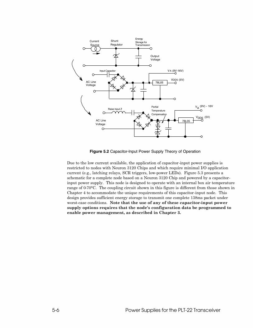
5-6 Power Supplies for the PLT-22 Transceiver
Energy Storage for Transmission
Current Source
Shunt Regulator
Output Voltage
AC Line Voltage
VA (9V-16V)
VDD5 (5V)78L05
AC Line
Voltage78L05
Raise Input ZPartial
Temperature
CompensationV
Input Capacitor
(5V)DD5
V (9V) - 16VA
Figure 5.2 Capacitor-Input Power Supply Theory of Operation
Due to the low current available, the application of capacitor-input power supplies is restricted to nodes with Neuron 3120 Chips and which require minimal I/O application current (e.g., latching relays, SCR triggers, low-power LEDs). Figure 5.3 presents a schematic for a complete node based on a Neuron 3120 Chip and powered by a capacitor-input power supply. This node is designed to operate with an internal box air temperature range of 0-70°C. The coupling circuit shown in this figure is different from those shown in Chapter 4 to accommodate the unique requirements of this capacitor-input node. This design provides sufficient energy storage to transmit one complete 138ms packet under worst-case conditions. Note that the use of any of these capacitor-input power supply options requires that the node's configuration data be programmed to enable power management, as described in Chapter 3.

LONWORKS PLT-22 in European Utility Applications 5-7
Figure 5.3 A-band Capacitor-Input Power Supply Schematic

5-8 Power Supplies for the PLT-22 Transceiver
Energy Storage Linear Supplies For products requiring minimal application current and safety isolation, an energy storage linear supply may be the smallest and most cost effective option. Consider a node based on a Neuron 3120 Chip, operating at 2.5MHz and consuming 1mA of application and I/O current. Using a linear power supply for the VA supply and a linear regulator for the VDD5 supply, the worst case current requirements are presented in Table 5.2.
Table 5.2 Example Worst-Case Node Current Consumption
Transmit Receive
PLT-22 VA 200mA 6mA
PLT-22 VDD5 18mA 20mA
Neuron 3120 Chip (@2.5MHz)
8mA 8mA
Application & I/O Current
1mA 1mA
78L05 Regulator Current
5mA 4mA
Total 232mA 39mA
A traditional linear supply would require a transformer with an output current rating of approximately 300mA. By taking advantage of the PLT-22 transceiver’s power management feature, an energy storage linear supply can be built with a 100mA transformer. Figure 5.4 shows an example of an energy storage linear supply.
AC Line
Voltage
V
V78L05
12.6 VAC @100 mA
4700 µF16 V±20%14 V, 5W
±5%IN5351B
+
A
DD5 (5V)
Figure 5.4 Energy Storage Linear Power Supply
Note that this supply is kept from exceeding the 16V maximum supply voltage rating of the PLT-22 transceiver by the inclusion of zener diode over-voltage protection. Without this diode, the combination of high AC line voltage and light output loading would result

LONWORKS PLT-22 in European Utility Applications 5-9
in output voltages >16V. In this application the zener diode does not conduct unless the output load is light and the line voltage is high.
In summary, an energy storage linear supply differs from a traditional linear supply in the following ways:
1. Allows the use of a smaller transformer;
2. Requires more output capacitance for energy storage;
3. May require over-voltage zener diode protection;
4. Requires that the node be programmed to enable power management, as described in chapter 3;
5. Under typical conditions, exhibits transmit duty cycles which are not limited. Over the full range of line voltage and component tolerance, the PLT-22 transceiver’s power management may act to regulate a particular node’s transmit duty cycle (to ≥10% in the above example).
Traditional Linear Power Supplies This option is usually suitable if the physical size of the power supply is not constrained in the application, since linear supplies tend to be physically larger than switching power supplies. Linear power supplies do not load the power line in the range of the PLT-22 transceiver's communication frequencies, nor do they generate significant noise. For these reasons, a linear power supply may be used without concern that communication performance will be adversely affected.
Switching Power Supplies While generally smaller than linear power supplies, switching power supplies can be a significant source of noise and power line signal attenuation. As a result the required design effort is significantly greater than that required for linear or capacitor-input power supplies.
Several design options are available for use if a switching power supply is required due to size or application current constraints. These options include a pre-designed switcher, an off-the-shelf switcher, and a custom-designed switcher. They are described following the discussion of switching supply design issues.
Power Supply-Induced Attenuation The input stage of a switching power supply typically contains an EMC filter that includes one or more capacitors connected directly from line to neutral and, in many cases, additional capacitors from line and neutral to ground. When the AC line terminals of the switching power supply are connected to the AC mains (in parallel with the coupling circuit), additional signal attenuation occurs. This loss can be avoided by inserting a series inductor between the power supply input and the power line communication channel as shown in figure 5.5.

5-10 Power Supplies for the PLT-22 Transceiver
Switching Power Supply
Coupling Circuit
PLT-22 Transceiver
Neuron Chip
Line
Neutral
Figure 5.5 Reducing Attenuation Caused by a Switching Power Supply
Including this inductor is desirable because the increase in attenuation for a given load is much worse when the load, in this case the switching power supply, is connected directly to the transceiver. In contrast, the loading caused by a switching supply that is separated from the receiver is reduced by the series inductance of power line wiring.
The value of the inductor should be chosen such that the power supply does not impose a low impedance onto the power line in the communication frequency range of 70kHz-95kHz. The appropriate value of inductance is a trade-off between required impedance, which is a function of system topology, and node cost. The selected inductor must have a current rating which is greater than the peak current drawn by the power supply in order to avoid impedance reduction due to inductor saturation. Higher impedances require larger inductance values which are more expensive for a given power supply input current.
For most AC mains distribution systems, where communication frequency impedances are typically in the range of 1 to 20 Ohms, a power supply input impedance of 100 Ohms is sufficient to avoid added signal attenuation.
To maximize communication distance on mains distribution systems between buildings where the system impedance may be as high as 50 Ohms, a minimum power supply input impedance of 250 Ohms is recommended. Table 5.3 shows the appropriate inductor value by application.
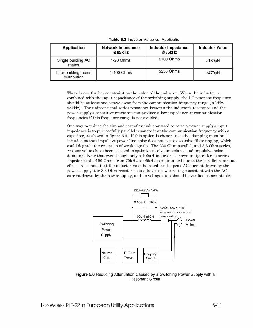
LONWORKS PLT-22 in European Utility Applications 5-11
Table 5.3 Inductor Value vs. Application
Application Network Impedance @85kHz
Inductor Impedance @85kHz
Inductor Value
Single building AC mains
1-20 Ohms ≥100 Ohms ≥180µH
Inter-building mains distribution
1-100 Ohms ≥250 Ohms ≥470µH
There is one further constraint on the value of the inductor. When the inductor is combined with the input capacitance of the switching supply, the LC resonant frequency should be at least one octave away from the communication frequency range (70kHz-95kHz). The unintentional series resonance between the inductor's reactance and the power supply's capacitive reactance can produce a low impedance at communication frequencies if this frequency range is not avoided.
One way to reduce the size and cost of an inductor used to raise a power supply's input impedance is to purposefully parallel resonate it at the communication frequency with a capacitor, as shown in figure 5.6. If this option is chosen, resistive damping must be included so that impulsive power line noise does not excite excessive filter ringing, which could degrade the reception of weak signals. The 220 Ohm parallel, and 3.3 Ohm series, resistor values have been selected to optimize receive impedance and impulsive noise damping. Note that even though only a 100µH inductor is shown in figure 5.6, a series impedance of ≥150 Ohms from 70kHz to 95kHz is maintained due to the parallel resonant effect. Also, note that the inductor must be rated for the peak AC current drawn by the power supply; the 3.3 Ohm resistor should have a power rating consistent with the AC current drawn by the power supply, and its voltage drop should be verified as acceptable.
CouplingCircuit
PLT-22
Txcvr
NeuronChip
Power MainsSwitching
Power
Supply
220Ω• ±5% 1/4W
3.3Ω• ±5%, •1/2W,wire wound or carboncomposition
0.039µF ±10%
100µH ±10%
Figure 5.6 Reducing Attenuation Caused by a Switching Power Supply with a Resonant Circuit

5-12 Power Supplies for the PLT-22 Transceiver
Noise at the Power Supply Input In order to achieve maximum communication performance and to comply with the conducted emissions specifications of CENELEC EN 50065-1, the switching power supply input must not conduct excessive noise onto the power mains. A switching power supply contains an oscillator that operates at a frequency between 10kHz and several MHz. Depending on the power supply design, significant energy at the switching frequency fundamental and/or its harmonics may appear at the input (line side) of the power supply. If the amplitude of the signal is large enough in sensitive frequency ranges, the performance of the PLT-22 transceiver may be degraded.
While the PLT-22 transceiver is designed to operate reliably with a combination of attenuation and significant switching supply noise, noise from the switching power supply closest to the receiver will have the most deleterious effect on communication performance. Noise from more distant sources will be attenuated before reaching a receiver, reducing its effect on reception.
Switching Power Supply Frequency Selection Selection of an appropriate operating frequency for a switching power supply will minimize the effect of switching noise on the PLT-22 transceiver's communication performance. By choosing an operating frequency such that the fundamental and harmonics of that switching supply avoid the transceiver's communication frequencies, the amount and cost of additional circuitry to filter interference from the switching supply can be minimized. In addition, it is recommended that switching frequencies in range of 110-140kHz be avoided to maximize compatibility with PLT-22 based nodes operating in the C-band. Table 5.4 below lists the optimal switching frequency ranges. The switching supply should be designed such that the fundamental switching frequency falls within the stated ranges under all line, load, environmental, and production conditions.
Table 5.4 Optimal Switching Power Supply Fundamental Operating Frequencies
Optimal Frequency Ranges
95kHz-110kHz
>140kHz
Switching Power Supply Input Noise Masks The noise "masks" presented below show the maximum noise allowable at the input of a switching power supply such that optimum performance of the PLT-22 transceiver is achieved and the appropriate conducted emissions specification is met. Figure 5.7 defines the noise mask for CENELEC EN 50065-1 conducted emissions compliance. The limits assume that the PLT-22 transceiver is used in conjunction with one of the recommended coupling circuits shown in Chapter 4.
Measurements of a particular power supply should be made by connecting the supply to the artificial mains network as specified in subclause 8.2.1 of CISPR Publication 16, second edition. Measurements should be made over the full range of anticipated loads on the supply since many switching supplies vary their switching frequency with load. Two different limits are shown. One limit is measured using a quasi-peak detector, the other using an average detector. Note that those limits are the same as required for any other

LONWORKS PLT-22 in European Utility Applications 5-13
CENELEC compliant product, except in the communication range of 70kHz to 95kHz where lower noise levels are specified.
The measurement bandwidths for these measurements are 200Hz for measurements below 150kHz, and 9kHz for measurements above 150kHz, as described in CISPR 16.
Figure 5.7 A-band Switching Power Supply Input Noise Limits for CENELEC EN 50065-1
Compliance
Table 5.5 lists the endpoints of the straight lines shown in figure 5.7.
20
30
40
50
60
70
80
90
100
110
1.0E+03 1.0E+04 1.0E+05 1.0E+06 1.0E+07 1.0E+08
Frequency (Hz)
Noi
se L
evel
(dB
uV)
Quasi-peak DetectorAverage Detector

5-14 Power Supplies for the PLT-22 Transceiver
Table 5.5 A-band Switching Power Supply Input Noise Limits for CENELEC EN 50065-1 Compliance
Frequency(kHz) Noise Level (dBuV): Quasi-Peak Detector
Noise Level (dBuV): Average Detector
9 89 N/A 40 77 N/A
40+ 70 N/A 70 70 N/A
70+ 40 N/A 90 40 N/A
90+ 70 N/A 150 66 56 500 56 46
500+ 56 46 5000 56 46
5000+ 60 50 30000 60 50
A power supply that does not meet the appropriate noise mask for the power supply input may require a filter between the local switching power supply and the power mains. A filter example which both attenuates switching supply noise and provides >200 Ohm input impedance is shown in figure 5.8. Note that both inductors must be rated for the peak AC current drawn by the power supply; the 3.3 Ohm resistor should have a power rating consistent with the AC current drawn by the power supply, and its voltage drop should be verified as acceptable.
CouplingCircuit
PLT-22
Txcvr
NeuronChip
Power
MainsSwitching
Power
Supply
220•Ω ±5% 1/4W
3.3Ω• ±5%, •1/2W,wire wound or carboncomposition
0.039µF ±10%
0.47µF ±20% X2 Type250VAC
100µH ±20% 100µH ±10%
Figure 5.8 A-band Optional Switching Power Supply LC Network
This filter has the attenuation characteristics shown in figure 5.9, when connected to
!

LONWORKS PLT-22 in European Utility Applications 5-15
a 50Ω mains network. If the supply noise drops by less than the values shown in figure 5.9. it is likely due to parasitic coupling between the two inductors. If this occurs, filtering close to the level shown in figure 5.9 can usually be accomplished by adjusting the relative location and orientation of the inductors (orthogonal orientation typically reduces inductor coupling). Alternately, shielded or toroidal inductors may be used to reduce coupling.
C
Communicationfrequencies(70 – 95kHz)
Figure 5.9 A-band Filter Frequency Response
In some instances it is possible that noise radiated from either the power supply or the supply filter may couple into the inductors of the transceiver's coupling circuit. The coupling circuit may then couple this noise onto the power mains. This problem can be diagnosed by disconnecting the transceiver's coupling circuit and then analyzing the conducted line noise.
If noise from parasitic coupling is suspected, it can be confirmed by inserting a 10cm (4") twisted wire pair in series with one of the inductors in question. If the conducted noise spectrum varies by more than a few dB when this inductor is moved closer to, and farther from, other components, then parasitic coupling may be the source of the problem.
There is a second, although less likely, potential cause for reduced filter effectiveness. It is possible for the inductive reactance of the filter components to be canceled by capacitive reactance from the input of the power supply. This problem is generally seen as narrow band noise which appears to pass through the filter unattenuated. This problem can be remedied by either damping the unintended resonance, or by adjusting the values of the filter inductor and capacitor to move the resonance to a non-interfering frequency. Damping may be accomplished by adding resistance in the range of 200 Ohms to 5k Ohms in parallel with the filter inductor closest to the power supply.

5-16 Power Supplies for the PLT-22 Transceiver
Switching Power Supply Output Noise Masks The PLT-22 transceiver requires +5VDC (VDD5) and +8.5VDC to +16VDC (VA) supply voltages. The amplitude of the noise and ripple on these power supply outputs must be controlled in order to comply with CENELEC EN 50065-1 as well as to achieve maximum communication performance. Noise "masks" are provided in figures 5.10 and 5.11. Figure 5.10 shows the recommended noise (ripple) limits on the VDD5 supply for CENELEC EN 50065-1 compliance. Figure 5.11 shows the recommended noise (ripple) limits on the VA supply for CENELEC EN 50065-1 compliance.
Measurements should be made over the full range of anticipated loads on the supply, since many switching supplies vary their switching frequency with load. For CENELEC EN 50065-1 measurements, a quasi-peak detector should be used. The measurement bandwidths are 200Hz for measurements below 150kHz, and 9kHz for measurements above 150kHz.
Figure 5.12 shows a probe that can be used to measure the noise on the power supplies. The twisted wires must be connected directly to the PLT-22 power and ground pins, and the coaxial cable must be connected to the 50Ω measuring equipment. Note that the 1/10 gain of the probe must be taken into account.
40
50
60
70
80
90
1.0E+04 1.0E+05 1.0E+06
Frequency (Hz)
Noi
se L
evel
(dB
uV)
Figure 5.10 A-band VDD5 Power Supply Noise Limits vs. Frequency for
CENELEC EN 50065-1 Compliance

LONWORKS PLT-22 in European Utility Applications 5-17
Figure 5.11 A-band VA Power Supply Noise Limits vs. Frequency for CENELEC EN 50065-1 Compliance
Table 5.6 and 5.7 lists the levels shown on the previous graphs in figures 5.11 and 5.12, respectively.
Table 5.6 A-band VDD5 Power Supply Noise Limits vs. Frequency for CENELEC EN 50065-1 Compliance
Frequency(kHz) Noise Level (dBuV) 10-70 80 70-90 50
90-200 65 200-300 70
300-1000 75
Table 5.7 A-band VA Power Supply Noise Limits vs. Frequency for CENELEC EN 50065-1 Compliance
Frequency(kHz) Noise Level (dBuV) 10-70 70 70-90 40
90-1000 70
30
40
50
60
70
80
1.0E+04 1.0E+05 1.0E+06
Frequency (Hz)
Noi
se L
evel
(dB
uV)
5-18 Power Supplies for the PLT-22 Transceiver
50cmmax
To PLT-22 SIPPower Supply
pins
To 50 Ωmeasuringequipment
50 Ω coax450 Ω
1µF
Figure 5.12 10x Power Supply Noise Probe
Options The following switching power supply options are available: pre-designed, off-the-shelf, and custom.
Pre-designed Switching Supplies This option is highly recommended if a small, low-cost power supply is desired and significant application current is required. Power Integrations has developed a power supply based on their TOP210 chip to specifically meet all of the design requirements for PLT-22 based nodes. This TOP210 design can supply a total of 400 mA at 12V and thus can support the PLT-22 transceiver, a Neuron Chip, plus about 100mA of application electronics. Detailed design information, including schematic and parts list, is available from Power Integrations in design note DN-15, TOPSwitch® Power Supply for Echelon PLT-21 Power Line Transceiver. This design note is available on the Power Integrations web site at http://www.powerint.com, or it can be ordered from Power Integrations at the following address:
Power Integrations, Inc. 477 North Mathilda Avenue Sunnyvale, CA 94086 Phone: +1-408-523-9200 or 1-800-552-3155 Fax: +1-408-523-9300
Building a power supply using DN-15 greatly simplifies the task of developing a switching supply-based PLT-22 node.
Off-the-Shelf Switching Supplies Most commercially available switching power supplies have been designed with some level of input noise filtering. Frequently this level of filtering is adequate if the supply’s fundamental switching frequency is within the optimal ranges of Table 5.4 over all operating conditions and tolerances. Supplies with other fundamental operating frequencies may be able to meet the required noise masks of the previous sections with greater effort and/or cost; however, meeting the noise mask requirements with a power supply fundamental frequency (or second or third harmonic) in the 70kHz to 95kHz range is very challenging and not recommended.
Most off-the-shelf switching supplies have a very low input impedance and require the addition of an input inductor as shown in figure 5.5.

LONWORKS PLT-22 in European Utility Applications 5-19
Custom Switching Supplies Design of a custom switching supply, even one which employs a commerically available controller chip, is very challenging and is only recommended if none of the other options outlined in this chapter are suitable. If this option is chosen, it is recommended that it only be pursued by experienced switching supply and electromagnetic compatibility experts. Even if such personnel are available, extra time must be allowed for design iterations during development. If this approach is chosen, it is absolutely essential that the supply is verified to meet the input and output noise masks of this chapter.

5-20 Power Supplies for the PLT-22 Transceiver
LONWORKS PLT-22 in European Utility Applications 6-1
6
Design and Test for Electromagnetic Compatibility
This chapter includes discussions of radiated electromagnetic interference (EMI) and electrostatic discharge (ESD) design practices for products containing the PLT-22 transceiver. These design practices help the designer to create a product with the required Electromagnetic Compatibility (EMC).
6-2 Design and Test for Electromagnetic Compatibility
EMI Design Issues The high-speed digital signals associated with microcontroller designs can generate unintentional electromagnetic interference (EMI). High-speed voltage transitions generate RF currents that can radiate from a product if a nearby length of wire or piece of metal acts as an antenna.
Products that use a PLT-22 transceiver together with a Neuron Chip will generally need to demonstrate compliance with EMI limits enforced by various regulatory agencies.
In addition to the following discussion, designers of PLT-22 transceiver-based nodes are strongly encouraged to read reference [9] for a good treatment of EMC. The EDN Designer's Guide to EMC10 is also a good source of design advice regarding EMC issues.
Designing Systems for EMC (Electromagnetic Compatibility) Careful PCB layout is important to ensure that a PLT-22 transceiver-based node will achieve the desired level of EMC. A typical PLT-22 transceiver-based node will have several digital signals switching in the 1MHz-10MHz range. These signals will generate both voltage noise near the signal traces, and current noise in the signal and power supply traces. The goal of good node design is to keep voltage and current noise from coupling out of the product enclosure.
It is very important to minimize the “leakage” capacitance from circuit traces in the node to any external metal near the node because this capacitance provides a path for the digital noise to couple out of the product enclosure. Figure 6.1 shows the leakage capacitances to earth ground from a node's logic ground (Cleak,GND) and from a digital signal line in the node (Cleak,SIGNAL ). If the PLT-22 transceiver-based node is housed inside a metal chassis, then that metal chassis will probably have the largest leakage capacitance to other nearby pieces of metal. If the node is housed inside a plastic package, then PCB ground guarding must be used to minimize Cleak,SIGNAL . Effective guarding of digital traces with logic ground reduces Cleak,SIGNAL significantly, which in turn reduces the level of common-mode RF currents driven onto the AC mains.
When a node is mounted near a piece of metal, especially metal that is earth grounded, any leakage capacitance from fast signal lines to that metal will provide a path for RF currents to flow. When Vgate is pulled down to logic ground, the voltage of logic ground with respect to earth ground will increase slightly. When Vgate pulls up to VDD5, logic ground will be pushed down slightly with respect to earth ground. As Cleak,SIGNAL increases, a larger current flows during Vgate transitions, generating more common-mode RF current. This common-mode RF current can generate EMI in the 30MHz-300MHz frequency band, thereby exceeding CENELEC levels, even when Cleak,SIGNAL from a clock line to earth ground is less than 1pF. This means that it is essential to guard the clock lines.

LONWORKS PLT-22 in European Utility Applications 6-3
Power Mains
Leakage Capacitances to Earth Ground
C leak,GND
C loadP
LT-2
2 an
d P
ower
Sup
ply
Node Logic Ground
C decouple
C leak,SIGNAL
Vgate
VDD5
GND
"CHASSIS" GND
C leak,CHASSIS
L
N
Cou
plin
g C
ircui
t
VDD5
Figure 6.1 Parasitic Leakage Capacitances to Earth Ground
From this discussion, it is apparent that minimizing Cleak,SIGNAL is very important. By using 0.1µF or 0.01µF decoupling capacitors at each digital IC power pin, VDD5 and logic ground noise can be reduced. Logic ground can then be used as a ground shield for other noisy digital signals and clock lines.
For example, with a PLT-22 transceiver-based A-band node that uses the Neuron 3120 Chip, one of the fastest digital signals on the PCB is the CP2(BCLK) line from the PLT-22 transceiver to the Neuron Chip. If a two-layer PCB is being used, CP2 can be routed to the Neuron Chip with a ground guard trace between the CP traces on the component side of the board, or a wide ground trace (or ground plane) covering the underside of the CP traces on the solder side of the PCB. If a four-layer PCB is used, the high-speed traces can be moved to inner layers and guarded on all four sides.
Since the Neuron 3150 Chip has an external memory interface bus, there are many more traces in a node using a Neuron 3150 Chip that need to be guarded by logic ground. In addition, the VDD5 noise generated by the memory interface and external ROM/RAM components requires more VDD5 decoupling, and may require a four-layer PCB to maintain RF-quiet VDD5 and logic ground lines.

6-4 Design and Test for Electromagnetic Compatibility
In summary, the following general rules apply:
• the faster the Neuron Chip clock speed, the higher the level of EMI;
• better VDD5 decoupling quiets RF noise at the sources (the digital ICs), which lowers EMI;
• the Neuron 3120 Chip generates less EMI than the Neuron 3150 Chip since the Neuron 3120 Chip has no external memory interface lines;
• a four-layer PCB generates less EMI than a two-layer PCB since the extra layers facilitate better VDD5 decoupling and more effective logic ground guarding;
• a two-layer PLT-22 transceiver-based node using on a Neuron 3120 Chip operating at 5MHz should be able to meet CENELEC EMC if good decoupling and ground guarding of the CKOUT line are used.
Early testing of prototype circuits at an outdoor EMI range should be used to determine the effectiveness of these EMC techniques.
ESD Design Issues Electrostatic discharge (ESD) is encountered frequently in industrial and commercial use of electronic systems8. In addition, the European Community has adopted requirements for ESD testing in product qualifications analogous to the present EMI requirements11 under the EMC directive.
Reliable system designs must consider the effects of ESD and take steps to protect sensitive components. Static discharges occur frequently in low-humidity environments when operators touch electronic equipment. Keyboards, connectors, and enclosures may provide paths for static discharges to reach ESD sensitive components such as the Neuron Chip and the PLT-22 transceiver. This section describes the issues involved in designing ESD immunity into PLT-22 transceiver-based products.
In addition to the following discussion, designers of PLT-22 transceiver-based nodes are strongly encouraged to read references [8] and [10]. The EDN Designer's Guide to EMC12 is especially helpful in understanding the importance of managing ESD return currents.
Designing Systems for ESD Immunity
There are two general methods that are used to protect products from ESD. The first is to seal the product to prevent static discharges from reaching the sensitive circuits inside the package. The second method involves grounding circuits so that ESD hits to user-accessible metal parts can be shunted around any sensitive circuitry.
For safety reasons, PLT-22 transceiver-based nodes that communicate on the AC mains generally do not have a user-accessible network connection. The product's package should be designed to minimize the possibility of ESD hits arcing into the node's circuit board. If the product's package is plastic, then the PCB should be supported in the package so that unprotected circuitry on the PCB is not adjacent to any seams in the package. The PCB should not touch the plastic of an enclosure near a seam, since a
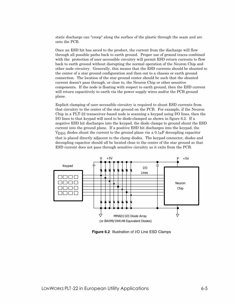
LONWORKS PLT-22 in European Utility Applications 6-5
static discharge can "creep" along the surface of the plastic through the seam and arc onto the PCB.
Once an ESD hit has arced to the product, the current from the discharge will flow through all possible paths back to earth ground. Proper use of ground traces combined with the protection of user-accessible circuitry will permit ESD return currents to flow back to earth ground without disrupting the normal operation of the Neuron Chip and other node circuitry. Generally, this means that the ESD currents should be shunted to the center of a star ground configuration and then out to a chassis or earth ground connection. The location of the star ground center should be such that the shunted current doesn't pass through, or close to, the Neuron Chip or other sensitive components. If the node is floating with respect to earth ground, then the ESD current will return capacitively to earth via the power supply wires and/or the PCB ground plane.
Explicit clamping of user-accessible circuitry is required to shunt ESD currents from that circuitry to the center of the star ground on the PCB. For example, if the Neuron Chip in a PLT-22 transceiver-based node is scanning a keypad using I/O lines, then the I/O lines to that keypad will need to be diode-clamped as shown in figure 6.2. If a negative ESD hit discharges into the keypad, the diode clamps to ground shunt the ESD current into the ground plane. If a positive ESD hit discharges into the keypad, the VDD5 diodes shunt the current to the ground plane via a 0.1µF decoupling capacitor that is placed directly adjacent to the clamp diodes. The keypad connector, diodes and decoupling capacitor should all be located close to the center of the star ground so that ESD current does not pass through sensitive circuitry as it exits from the PCB.
+5V +5V
Keypad
Neuron
Chip
MMAD1103 Diode Array
(or BAV99/1N4148 Equivalent Diodes)
I/O
Lines
Figure 6.2 Illustration of I/O Line ESD Clamps
6-6 Design and Test for Electromagnetic Compatibility
Conducted Emissions Testing When used with one of the recommended coupling circuits from Chapter 4, the PLT-22 transceiver is designed to comply with CENELEC EN 50065-1 “Signaling on low-voltage electrical installations in the frequency range 3kHz to 148.5kHz” Part 1 “General requirements, frequency bands and electromagnetic disturbances”.
Many commercial testing laboratories lack experience measuring conducted emissions of intentional power line communicators, and commonly-applied testing procedures will give erroneous measurement results. Proper measurement of conducted emissions to verify compliance with CENELEC EN 50065-1 requires strict adherence to the following guidelines.
• Connect the product under test to the correct network for measurement. CENELEC EN 50065-1 measurements use the 50Ω//(50µH+5Ω) Line Impedance Stabilization Network (LISN) as specified in CISPR Publication 16(7), second edition.
• Care must be taken to ensure that the PLT-22 transceiver's transmit signal does not overload the measurement apparatus. Typically, an attenuator must be installed at the input to the measuring receiver, i.e., spectrum analyzer, to avoid erroneous results due to instrumentation overload. A test for determining whether or not the results are being distorted due to overload is as follows: measure the emissions, then increase the attenuation between the product under test and the measuring receiver, and then re-measure emissions. There is an overload problem if the level of emissions at frequencies other than the main carrier has decreased by more than the increase in attenuation. Most spectrum analyzers have a built-in input attenuator. If this is the case, the attenuator setting is usually taken into account by the instrument. Consequently, the reported levels should not change when the spectrum analyzer input attenuation is changed. There is an overload problem if a level change is reported at frequencies other than the main carrier frequency.
• Care must be taken to ensure that the residual noise floor of the entire measurement set remains at least 10dB below the specification limit once the appropriate attenuator is installed. That is, a noise floor less than 36dBµV for CENELEC EN 50065-1 measurements.
• The measurements must be made with the specified detector. CENELEC EN 50065-1 measurements use the quasi-peak detector and the average detector as specified in CISPR Publication 16. Although a scan with a peak detector is common because it may be performed quickly, the limits specified by CENELEC EN 50065-1 are for quasi-peak and average detectors only. For power line transceivers, peak measurements often appear erroneously high relative to the quasi-peak limits.
• The measurements must be made with the specified filter. For CENELEC EN 50065-1 measurements, a 200Hz bandwidth filter is specified for measurements below 150kHz, and a 9kHz bandwidth filter is specified above 150kHz.
• The CENELEC EN 50065-1 specification requires that the filter inside the measuring receiver have even steeper filter skirts than the minimum required by CISPR 16.
LONWORKS PLT-22 in European Utility Applications 6-7
The CENELEC EN 50065-1 sub-committee SC 105A (Mains Communicating Systems) recognized the need for a filter with steeper skirts than the minimum specified by CISPR Publication 16. As stated in a final draft of an amendment to EN 50065-1 dated January, 1994, "the measuring instrument defined by the minimum requirements of CISPR 16 is unsuitable for the measurement of mains signaling equipment that uses a signaling frequency not far below 150kHz," and the sub-committee SC 105A agreed that "the proper solution would be to specify the attenuation characteristic of the measuring receiver more closely, receivers being known to be available on the market."1 EN 50065-1 Amendment AC specifies a filter that still complies with CISPR 16 but which has steeper filter skirts. Many spectrum analyzers, even very expensive ones, do not meet this requirement.
The Rohde&Schwarz EMI Test Receiver ESHS30 has been found to have adequate filter skirts. Although its specification does not guarantee adequate filter skirts, two samples of the ESHS30 test receiver were found to make the measurement reliably.
In addition, care must be taken in setting up the Rohde&Schwarz EMI Test Receiver ESHS30. The "automatic" mode for setting input attenuation selects an incorrect attenuation level that will result in an overload condition, which is not properly reported by the overload indicator on the Test Receiver. The proper attenuation must be selected using manual mode. A set-up program to accurately run scans for CENELEC EN 50065-1 compliance testing on the Rohde&Schwarz EMI Test Receiver ESHS30 is available from Echelon's LONWORKS Developer's Toolbox at www.echelon.com/toolbox.
An application note from Hewlett-Packard5 describes a test method for performing EN 50065-1 conducted emissions tests using Hewlett-Packard EMI test receivers. The title of the application note is “Conducted Emissions Measurements on Power Line Transceiver Products.” This application note describes an “off-the-shelf” external filter and a methodology that allows the measurements specified in EN 50065-1 to be performed accurately.
If the unit under test is found to exceed the applicable conducted noise limit at frequencies above 500kHz, it may be the result of unintentional coupling from the node's various digital circuits. If this occurs, improvements in grounding and printed circuit layout are generally required. Refer to Chapter 4 for a discussion of how to avoid coupling circuit stray field pickup.
In some instances conducted emissions above 500kHz can be adequately reduced by the addition of a small value capacitor (e.g., ≤3600pF) either across the AC mains or from the line conductor to ground. While nodes using the PLT-22 transceiver have been demonstrated to pass various limits without an additional capacitor, variations in node design and layout may require the addition of this small value capacitor. If a capacitor is added across the line it should be an X2 safety-rated type for maximum surge reliability. If capacitors are added from either line or neutral to earth, they should be Y safety rated. Alternately, this capacitor can be added across coupling circuit inductor L1 (see figure 4.9) or across the secondary winding of transformer T1 (see figures 4.10 and 4.12). If this option is chosen, either a metalized polyester capacitor ≥400VDC, a ceramic 1000VDC capacitor, or a Y-type capacitor should be used for surge reliability.
Adding capacitance in any of the above locations reduces the input impedance of the node and could therefore cause an increase in communication signal attenuation. The maximum value of capacitance which can be added without significantly affecting attenuation depends on the application. Table 6.1 shows the maximum value of added
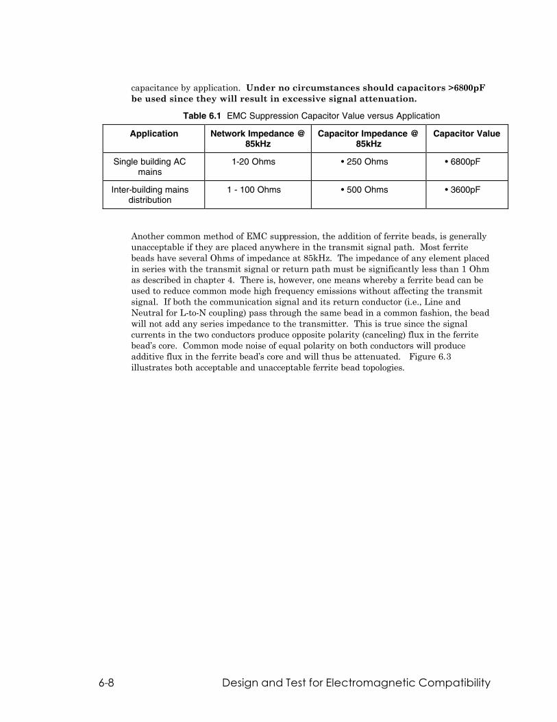
6-8 Design and Test for Electromagnetic Compatibility
capacitance by application. Under no circumstances should capacitors >6800pF be used since they will result in excessive signal attenuation.
Table 6.1 EMC Suppression Capacitor Value versus Application
Application Network Impedance @ 85kHz
Capacitor Impedance @ 85kHz
Capacitor Value
Single building AC mains
1-20 Ohms • 250 Ohms • 6800pF
Inter-building mains distribution
1 - 100 Ohms • 500 Ohms • 3600pF
Another common method of EMC suppression, the addition of ferrite beads, is generally unacceptable if they are placed anywhere in the transmit signal path. Most ferrite beads have several Ohms of impedance at 85kHz. The impedance of any element placed in series with the transmit signal or return path must be significantly less than 1 Ohm as described in chapter 4. There is, however, one means whereby a ferrite bead can be used to reduce common mode high frequency emissions without affecting the transmit signal. If both the communication signal and its return conductor (i.e., Line and Neutral for L-to-N coupling) pass through the same bead in a common fashion, the bead will not add any series impedance to the transmitter. This is true since the signal currents in the two conductors produce opposite polarity (canceling) flux in the ferrite bead’s core. Common mode noise of equal polarity on both conductors will produce additive flux in the ferrite bead’s core and will thus be attenuated. Figure 6.3 illustrates both acceptable and unacceptable ferrite bead topologies.
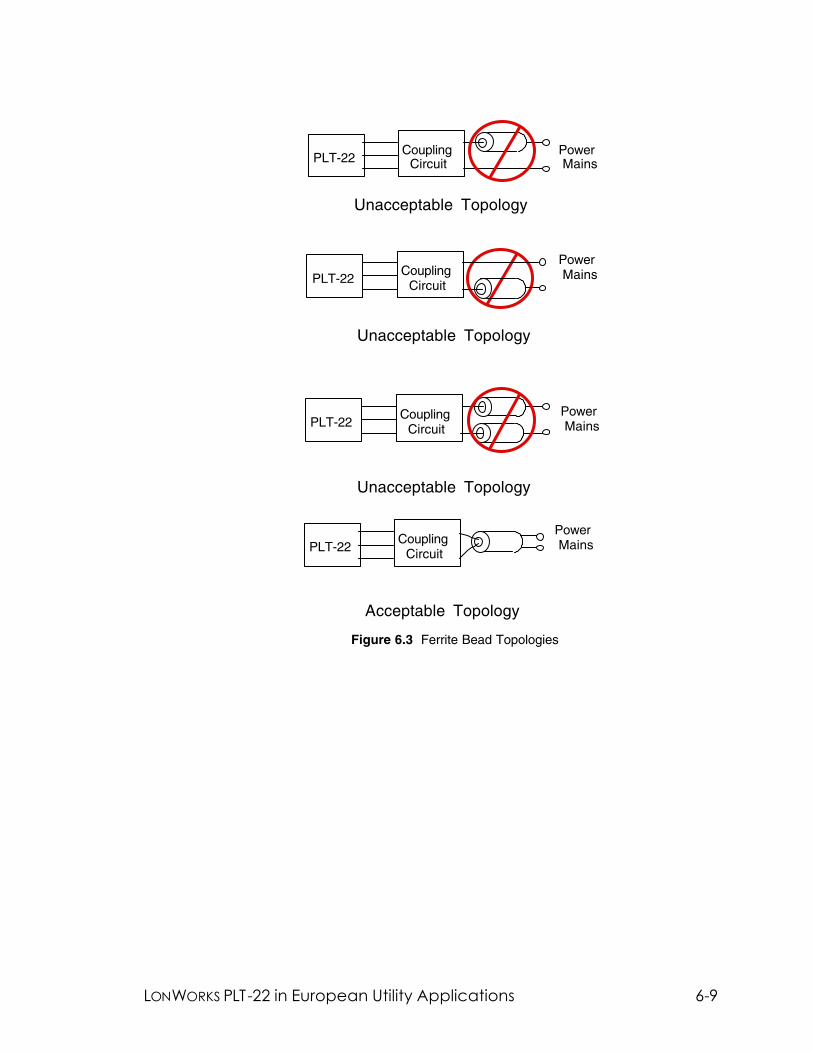
LONWORKS PLT-22 in European Utility Applications 6-9
Power MainsPLT-22
Coupling Circuit
Power MainsPLT-22
Coupling Circuit
Power MainsPLT-22
Coupling Circuit
Unacceptable Topology
Unacceptable Topology
Unacceptable Topology
Power MainsPLT-22
Coupling Circuit
Acceptable Topology
Figure 6.3 Ferrite Bead Topologies

6-10 Design and Test for Electromagnetic Compatibility

LONWORKS PLT-22 in European Utility Applications 7-1
7
Communication Performance Verification
This chapter describes procedures to verify basic communication performance of products based on the PLT-22 transceiver.
7-2 Communication Performance Verification
Why Verify Communication Performance? While each PLT-22 transceiver is verified to meet its full communication performance capabilities prior to shipment, circuitry external to the transceiver could compromise the communication performance of the node in which the transceiver is used. Ways in which communication performance could be compromised include mis-loaded components, inadequately filtered switching power supplies, circuitry improperly added between the transceiver's coupling circuit and the power mains, and deviations from recommended part specifications. Due to the robust communication capability of the transceiver, it may not be obvious that communication performance has been compromised when testing in a nominal environment.
Since compromised performance is generally observable only under “corner-case” conditions, failure to verify performance prior to deployment could result in many marginal units in the field before a problem is detected. It is therefore essential that the communication performance of every PLT-22-based design be verified prior to field deployment. This can be accomplished either by self verification, using the procedures given in this chapter, or by contacting your Echelon sales representative to make arrangements to send the node to Echelon for a confidential evaluation.
This chapter describes a simple "black box" testing methodology for determining whether or not the communication performance of a PLT-22 transceiver-based product has been compromised.
Before starting the verification process it is essential that the checklist in Appendix C be completed in its entirety.
Verification Strategy An overview of the recommended verification procedure is as follows:
1 Create a controlled power line environment that is isolated from typical power mains noise and loading.
2 Provide known load impedances at the PLT-22 transceiver's communication
frequencies. 3 Use the PLCA-22 Power Line Communications Analyzer (model 58022) as a
calibrated reference transmitter and receiver. 4 Test the performance independent of the product's application by making use of
the Neuron Chip service pin and internal statistics features. If the product under test does not have a service pin switch then it will need to be added to the product for testing purposes.
5 Test for unintentional noise injection and excessive loading by the product under
test. This is to ensure that the device can behave as a “good citizen” on a power line network.
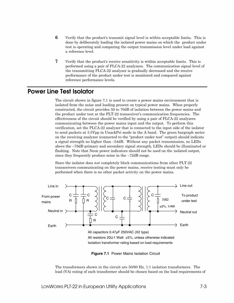
LONWORKS PLT-22 in European Utility Applications 7-3
6 Verify that the product's transmit signal level is within acceptable limits. This is done by deliberately loading the isolated power mains on which the product under test is operating and comparing the output transmission level under load against a reference level.
7 Verify that the product's receive sensitivity is within acceptable limits. This is
performed using a pair of PLCA-22 analyzers. The communication signal level of the transmitting PLCA-22 analyzer is gradually decreased and the receive performance of the product under test is monitored and compared against reference performance levels.
Power Line Test Isolator The circuit shown in figure 7.1 is used to create a power mains environment that is isolated from the noise and loading present on typical power mains. When properly constructed, the circuit provides 50 to 70dB of isolation between the power mains and the product under test at the PLT-22 transceiver’s communication frequencies. The effectiveness of the circuit should be verified by using a pair of PLCA-22 analyzers communicating between the power mains input and the output. To perform this verification, set the PLCA-22 analyzer that is connected to the input side of the isolator to send packets at 3.5Vpp in UnackPri mode in the A band. The green bargraph meter on the receiving analyzer (connected to the “product under test” output) should indicate a signal strength no higher than –54dB. Without any packet transmission, no LEDs above the –78dB primary and secondary signal strength, LEDs should be illuminated or flashing. Note that Neon power indicators should not be used on the isolated output, since they frequently produce noise in the –72dB range.
Since the isolator does not completely block communications from other PLT-22 transceivers communicating on the power mains, receive testing must only be performed when there is no other packet activity on the power mains.
All capacitors 0.47µF 250VAC (X2 type)
All resistors 20Ω 1 Watt ±5%, unless otherwise indicated
Isolation transformer rating based on load requirements
Line in
Neutral in
Earth
Line out
Neutral out
Earth
From power
mains
To product
under testR
C
R
R
CC C
CC
±5%, 1/4W
C50Ω
Figure 7.1 Power Mains Isolation Circuit
The transformers shown in the circuit are 50/60 Hz, 1:1 isolation transformers. The load (VA) rating of each transformer should be chosen based on the load requirements of

7-4 Communication Performance Verification
the devices under test. Care should be taken when wiring the isolator to avoid inadvertent signal coupling between the input and output wiring by spacing the input and output wires at least 15cm (6") apart.
Test Equipment In addition to the power mains isolator described in the previous section, the following “off-the-shelf” equipment will be needed for testing:
• One pair of PLCA-22 Power Line Communications Analyzers (model 58022).
• One PL-20 Line-to-Neutral power line coupler, Echelon model 78200-221.
• Two 50Ω coax cables approximately 25cm (12") long with male BNC connectors on both ends (AMP 1-221128-x or equivalent).
• A power strip, equipped with both a circuit breaker and 4 or more outlets, which does not include either surge protection, neon light, or noise isolation circuitry.
The following additional equipment will need to be constructed for testing:
• A "5Ω load" circuit, as shown in figure 7.2, should be built in a suitable enclosure and provided with an appropriate male AC mains plug. Note that the 1MΩ resistor’s stand-off voltage should be greater than or equal to the peak line voltage.
±5%,1/4W
0.47µF ±10%, 250VAC (X2 type)
L
N
E open
1MΩ,
4.7Ω±5%, 1W
Figure 7.2 "5Ω load" Circuit
• An impedance circuit shown in figure 7.3 should be built in a suitable enclosure with bulkhead BNC jacks (AMP 413771-x or equivalent). This impedance circuit, placed in series with the output path of a PLCA-22 analyzer, effectively increases its output impedance. This will allow for a more sensitive measurement of the receive mode impedance of the product under test.
88.7Ω ±1%,
Figure 7.3 Impedance Circuit Used For Excessive Loading Verification

LONWORKS PLT-22 in European Utility Applications 7-5
• An attenuation circuit shown in figure 7.4 should be built in a suitable enclosure with bulkhead BNC jacks (AMP 413771-x or equivalent). This attenuation circuit, or "pad", will provide approximately 60dB of attenuation when connected into the receive performance verification set-up of figure 7.8.
30.1kΩ ±1%, 1/4W
Figure 7.4 Attenuation Circuit Used For Receive Performance Verification
For the receive performance verification, a PC running the nodeutil.exe (available on the Echelon’s Developer’s Toolbox at www.echelon.com/toolbox) is required. The Node Status command will be used to obtain a record of the number of uncorrupted packets received by the Unit Under Test (UUT). This setup is described in detail in Receive Performance Verification, later in this chapter.
Good Citizen Verification Use the following steps to verify that the Unit Under Test (UUT) does not inject unwanted noise onto the power mains or excessively load the power mains.
Unintentional Output Noise Verification The following procedure determines if the UUT is generating unwanted noise which may hinder its communication performance or that of other devices on the power mains.
1 Connect a single PLCA-22 analyzer, the UUT, and the Isolator as shown in figure 7.5. Verify that the analyzer is set for A-band operation by observing the selected band in the upper right-hand corner of the LCD display (If it is set for C-Band, then it must be changed to A-Band using the setup screen of the analyzer.) Leave the PLCA-22 analyzer in idle mode (no packets being transmitted) and set it for Internal and Line-to-Neutral coupling (coupling mode switch to the right).
2 Verify that the UUT application program is not sending messages.
3 Observe the signal strength bar graph LEDs. None of the LEDs above the -72dB LED, should be on or flashing on either the primary or secondary bar graph meters. In addition, the Packet Detect (PKD) LEDs should not flash any more than once per minute.

7-6 Communication Performance Verification
Unit Under Test
(UUT)
service pin
PLCA-22
To powermains
packet detect LED
ISOLATOR
Recv
Isloated Power Line
A-band
Figure 7.5 A-band Unintentional Output Noise Verification
If any of the signal strength LEDs above the -72dB LEDs, are on or flashing, or the PKD LEDs flash more than once per minute, then excessive noise or interference is present. This could be caused by one or more of the following sources:
• The UUT is generating unwanted noise internally. This is most often associated with on-board switching power supplies. If the UUT includes a switching power supply, verify that the power supply noise masks of Chapter 5 have been met.
• Power line communications signals present on the power input side of the isolator are
not sufficiently attenuated. Ensure that no other power line signaling equipment is operating on the power mains when performing this test.
• The isolator is not completely isolating the test set-up from noise on the power mains.
Verify the effectiveness of the isolator as described earlier.
The source of this noise or interference must be identified and eliminated before proceeding with verification testing.
Excessive Loading Verification The procedure described in this section is used to determine if the receive mode impedance of the UUT is greater than approximately 100Ω at 86kHz (as it should be).

LONWORKS PLT-22 in European Utility Applications 7-7
A receive mode impedance of less than 100Ω could cause excessive signal attenuation resulting in impaired reception by both the UUT and its neighboring nodes. For applications which require an even higher receive impedance, refer to discussions in Chapters 5 and 6.
The 10Vp-p output capability of the PLCA-22 analyzer is used to increase the sensitivity of the test. The higher output signal allows the 0dB, -3dB, and -6dB LEDs of the PLCA-22 analyzer signal strength meter to be used for observing signal strength. These LEDs, unlike the other LEDs in the signal strength meter, are only 3dB apart allowing for better measurement resolution.
A series impedance circuit (figure 7.3) in the output path of the transmitting PLCA-22 analyzer is used to increase its effective output impedance, thereby preventing its normally low transmit output impedance from overshadowing the impedance of the product under test.
1 Set a PLCA-22 analyzer in Recv, UnackPr, and A-band modes (referred to as the Recv PLCA-22 analyzer) and configured for Internal and Line-to-Neutral coupling, as shown in figure 7.6.
2 Connect a second PLCA-22 analyzer in Send, UnackPri, and A-band modes (referred to as the Send PLCA-22 analyzer) and set it for External and Line-to-Neutral coupling as shown in figure 7.6. Connect the impedance circuit (88.7Ω resistor) and the coupling circuit as shown.
3 Verify that Attn on the SPHY PLCA-22 analyzer is set to 0. Set the number of packets to be transmitted to 9999k on that unit and set the packet length to 13 bytes. Set TxVpp: 10V.
4 Without the UUT connected, press START on the Send PLCA-22 analyzer. A test should begin and the receive packet count on the Recv PLCA-22 analyzer should increment with a packet error rate very close to 0%. The signal strength meter on the Recv PLCA-22 analyzer should have the LEDs up to and including the -3dB primary signal strength LED illuminated. The 0dB primary LED may or may not be flashing.
5 Next, connect the UUT as shown in figure 7.6. The -3dB primary signal strength LED on the Recv PLCA-22 analyzer either should be flashing or illuminated continuously. If the -3dB primary LED is extinguished, then the UUT's input impedance is excessively low (<100Ω). The impedance of the UUT must be corrected before proceeding; refer to the node checklist described in Appendix C for assistance.

7-8 Communication Performance Verification
Unit Under Test
(UUT)
service pin
PLCA-22
ISOLATOR
To powermains
packet detect LED
Recv
See text before powering unit.
PLCA-22
SendImpedance
Circuit(see fig. 7-3)
coax
coax
TxVpp:10VPL-20L-N 240VCoupler
IsolatedPowerLine
A-band
A-band
Figure 7.6 Excessive Loading Verification
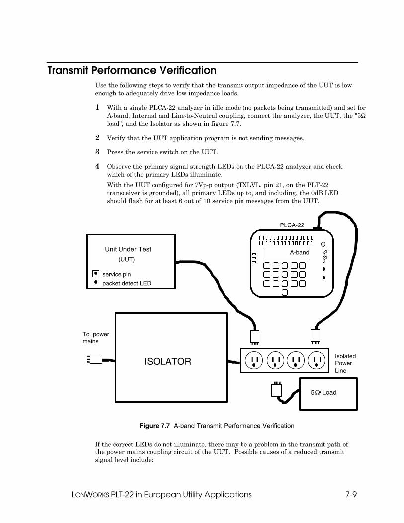
LONWORKS PLT-22 in European Utility Applications 7-9
Transmit Performance Verification Use the following steps to verify that the transmit output impedance of the UUT is low enough to adequately drive low impedance loads.
1 With a single PLCA-22 analyzer in idle mode (no packets being transmitted) and set for A-band, Internal and Line-to-Neutral coupling, connect the analyzer, the UUT, the "5Ω load", and the Isolator as shown in figure 7.7.
2 Verify that the UUT application program is not sending messages.
3 Press the service switch on the UUT.
4 Observe the primary signal strength LEDs on the PLCA-22 analyzer and check which of the primary LEDs illuminate.
With the UUT configured for 7Vp-p output (TXLVL, pin 21, on the PLT-22 transceiver is grounded), all primary LEDs up to, and including, the 0dB LED should flash for at least 6 out of 10 service pin messages from the UUT.
Unit Under Test
(UUT)
service pin
PLCA-22
To powermains
packet detect LED
ISOLATORIsolatedPowerLine
5Ω• Load
A-band
Figure 7.7 A-band Transmit Performance Verification
If the correct LEDs do not illuminate, there may be a problem in the transmit path of the power mains coupling circuit of the UUT. Possible causes of a reduced transmit signal level include:

7-10 Communication Performance Verification
• Additional series impedance has been inadvertently added between the PLT-22 transceiver's coupling circuit and the mains connection.
• The DC resistance of the series resonant inductor in the coupling circuit (L2 in Chapter 4 coupling circuit figures) is too high.
• The UUT contains a line fuse that has high series resistance.
• A component of the wrong value has been inadvertently used in the UUT.
• Inadequate analog power supply (VA) voltage under conditions of full transmit current loading.
Refer to the node checklist in Appendix C for more information about verifying the UUT's design.
Receive Performance Verification The receive performance verification procedure requires a software tool to measure the number of uncorrupted packets received by the UUT. Packet error rate is then calculated based on the number of packets sent and the number correctly received. A utility program to monitor packet activity is described below, before a description of the verification procedure.
Packet Error Measurement with Nodeutil A DOS utility called nodeutil.exe will be used to measure packets correctly received by the UUT. The Nodeutil software allows a PC to remotely query the UUT and extract its status, including uncorrupted packets received by the node (stored in every Neuron Chip). The nodeutil.exe utility is available free of charge from Echelon’s Web site at www.echelon.com/toolbox.
Figure 7.8 illustrates the setup for the PC running the Nodeutil utility. The PC should contain a PCLTA-20 network interface equipped with a PLM-22 SMX transceiver configured for A-band use. The adapter is connected to the isolated power line via a PL-20 power line coupler.
The DOS driver for the network adapter, ldvpclta.sys, should be used by adding the following line to the config.sys file on the PC:
device:c:\[path]\ldvpclta.sys [options]
The latest version of ldvpclta.sys is available from Echelon’s Web site. Refer to the PCLTA-20 network adapter user's guide or detailed information about the driver set-up and its options.
The nodeutil.exe program runs on the PC (under DOS) and accesses the UUT over the power line. The verification procedure below describes how to use the Nodeutil utility to access the UUT.
The startup screen for the Nodeutil utility is shown below. Refer to the nodeutil.txt file for information on its proper setup.
Node Utility Release 1.46
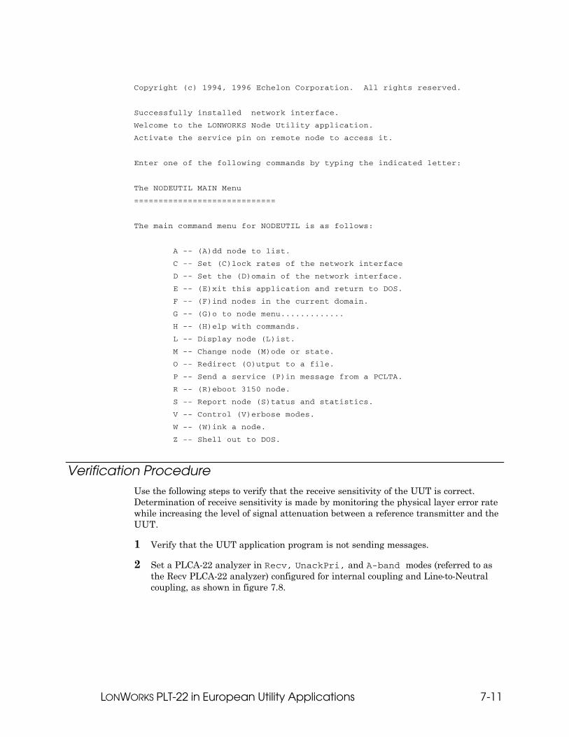
LONWORKS PLT-22 in European Utility Applications 7-11
Copyright (c) 1994, 1996 Echelon Corporation. All rights reserved.
Successfully installed network interface.
Welcome to the LONWORKS Node Utility application.
Activate the service pin on remote node to access it.
Enter one of the following commands by typing the indicated letter:
The NODEUTIL MAIN Menu
=============================
The main command menu for NODEUTIL is as follows:
A -- (A)dd node to list.
C -- Set (C)lock rates of the network interface
D -- Set the (D)omain of the network interface.
E -- (E)xit this application and return to DOS.
F -- (F)ind nodes in the current domain.
G -- (G)o to node menu.............
H -- (H)elp with commands.
L -- Display node (L)ist.
M -- Change node (M)ode or state.
O -- Redirect (O)utput to a file.
P -- Send a service (P)in message from a PCLTA.
R -- (R)eboot 3150 node.
S -- Report node (S)tatus and statistics.
V -- Control (V)erbose modes.
W -- (W)ink a node.
Z -- Shell out to DOS.
Verification Procedure Use the following steps to verify that the receive sensitivity of the UUT is correct. Determination of receive sensitivity is made by monitoring the physical layer error rate while increasing the level of signal attenuation between a reference transmitter and the UUT.
1 Verify that the UUT application program is not sending messages.
2 Set a PLCA-22 analyzer in Recv, UnackPri, and A-band modes (referred to as the Recv PLCA-22 analyzer) configured for internal coupling and Line-to-Neutral coupling, as shown in figure 7.8.
7-12 Communication Performance Verification
3 Set a second PLCA-22 analyzer in Send, UnackPri, and A-band modes (referred to as the Send PLCA-22 analyzer) and configure the coupling switch for external coupling. Connect the PLCA-22 analyzer using the attenuation circuit (30kΩ resistor; figure 7-4) and the PL-20 Line-to-Neutral coupler as shown in figure 7.8. Note that the line cord of the Send PLCA-22 analyzer is connected to the power mains on the input side of the isolator to prevent communications between the two PLCA-22 analyzers via parasitic line cord coupling.
4 Set the following parameters on the Send PLCA-22 analyzer:
Number of Packets = 1000 (1k) Packet Length = 13 bytes TxVpp = 7V Attn = 0 dB
5 Connect the UUT test setup as shown in figure 7.8. Once the Nodeutil utility is running correctly and the start-up screen shown above is displayed, press the service switch on the UUT. This will cause Nodeutil to register the service pin message received from the device. Select the “S” command to obtain the status from the UUT (the entry in the results screen named “Packets received by node” is the number of uncorrupted packets received by the UUT since the last time the statistics were cleared). Type “Y” at the prompt to clear the status of the UUT. The S command will be used in the next few steps to obtain the received packets count from the UUT. Be sure to clear the status of the UUT after each reading.
6 Press START on the Send PLCA-22 analyzer. The test will begin and the receive packet count on the Recv PLCA-22 analyzer should increment with a packet error rate very close to 0% (<1%). The -54dB LED on the primary frequency signal strength meter on the Recv PLCA-22 analyzer should illuminate, indicating that the received signal is approximately -60dB relative to the nominal 7Vp-p transmit signal (-54dB relative to the 3.5Vp-p meter scale). The -60dB attenuation level serves as a starting point; additional attenuation will be added via the Attn function of the Send PLCA-22 analyzer.
7 Once the Send PLCA-22 analyzer has transmitted 1000 packets, obtain the received packets count from the UUT using the "S" command of the Nodeutil utility software. Record that value and the packet error rate of the Recv PLCA-22's analyzer in columns 4 and 5 of table 7.1. Calculate the error value as a percentage (by subtracting the number of packets received by the node from 1011 and then dividing by 10) and record the result in the rightmost column of table 7.1. This procedure yields a sufficiently accurate approximation of the actual packet error rate. Refer to the notes at the end of these steps for details.
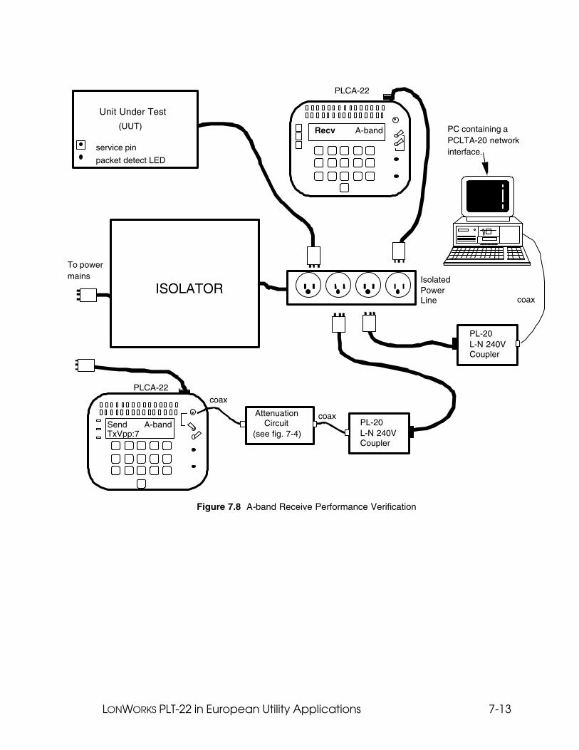
LONWORKS PLT-22 in European Utility Applications 7-13
Unit Under Test
(UUT)
service pin
PLCA-22
ISOLATOR
packet detect LED
PLCA-22
Send
coax
coax
Recv
TxVpp:7PL-20L-N 240VCoupler
coax
PL-20L-N 240VCoupler
PC containing aPCLTA-20 networkinterface.
AttenuationCircuit
(see fig. 7-4)
IsolatedPowerLine
To powermains
A-band
A-band
Figure 7.8 A-band Receive Performance Verification

7-14 Communication Performance Verification
8 After moving the cursor to the Attn field, press the CHANGE and ENTER keys on the Send PLCA-22 analyzer to increment the Attn level by 6dB. Then clear the status on the UUT by responding with a "Y" to the Nodeutil prompt and then press START on the Send PLCA-22 analyzer.
9 Repeat steps 7 through 8 above for all Send Attn levels up to, and including 24dB, recording the results each time in table 7.1.
10 To test the UUT's secondary operating frequency, change the PLCA-22 analyzers from UnackPri to UnackSec mode. Repeat steps 6 through 9, above, but record the results in table 7.2.
Notes:
The calculation of packet error rate used in the above verification avoids inaccuracies that would result from the use of the CRC error count to compute packet error rate. It does, however, make use of one simplifying approximation that does not alter the resultant observed sensitivity. The material in this note is provided for other applications where a precise measure of packet error rate may be required. Packet error rate actually includes both packets received with an incorrect CRC plus any packets which were so weak or corrupted they were not detected at all. These “missed packets” are, by definition, not included in the CRC error count of a node. For a physical layer packet error rate of 10%, the percentage of missed packets is generally negligible. Under conditions where the packet error rate is greater than 10%, a significant portion of the error rate may be due to missed packets. The “Packets received by node" field in Nodeutil software yields the actual number of packets correctly received by the node. Subtracting this number from the total number of packets sent gives the exact packet error count, including missed packets.
In addition to the number of test packets selected on the PLCA-22 analyzers, the total number
of packets sent on the power line actually includes several control packets sent between the PLCA-22 analyzers. These control packets are used by the PLCA-22 analyzers to synchronize their settings before the test, and to exchange data related to the test immediately after the test. Additionally, querying the status of the UUT causes some packets to be logged, the number of which will depend on the tool used and the firmware version number of the UUT’s Neuron Chip. This number can be determined by performing a non-attenuated, noise-free test with the PLCA-22 analyers and then observing the number of “Packets received by node” above the number of test packets defined on the PLCA-22 analyzer. The total overhead is generally either 11 or 13 packets.
Given the above, a more accurate formula for calculating the physical layer packet error rate
with 1000 test packets is then: PER% = (1011 - # “Packets received by node”) x 100 / 1011

LONWORKS PLT-22 in European Utility Applications 7-15
Table 7.1 Primary Frequency Receive Performance Verification Table
Send Transmit
Attenuation (PLCA Attn)
Overall Attenuation (Attn + 60)
UnackPri Error %
(expected)
UnackPri Error %
(observed)
UUT Pkts Received
(observed)
UUT Error %
(expected)
UUT Error %
(1011 - # Rcvd)/10 (observed)
0 dB 60 dB <1% <1%
6 dB 66 dB <2% <2%
12 dB 72 dB <3% <3%
18 dB 78 dB ~3% ~3%
24 dB 84 dB ≥3% ≥3%
Table 7.2 Secondary Frequency Receive Performance Verification Table
Send Transmit
Attenuation (PLCA Attn)
Overall Attenuation (Attn + 60)
UnackSec Error %
(expected)
UnackSec Error %
(observed)
UUT Pkts Received
(observed)
UUT Error %
(expected)
UUT Error %
(1011 - # Rcvd)/10 (observed)
0 dB 60 dB <1% <1%
6 dB 66 dB <3% <3%
12 dB 72 dB ~3% ~3%
18 dB 78 dB ≥3% ≥3%
The approximate signal attenuation between the Send PLCA-22 analyzer and Recv PLCA-22 analyzer shown in tables 7.1 and 7.2 is the sum of the attenuation level of the attenuator circuit and the Attn level of the Send PLCA-22 analyzer. A properly performing product will show a low level of errors (<3%) up to an attenuation of 72dB between the two analyzers (66dB for secondary frequency). Above these attenuations the error rate for the UUT should increase.
If the results of this test are worse than expected, it is helpful to know if the problem affects only the performance of the UUT or if adjacent receivers are also impaired by the presence of UUT. If the receive performance of the Recv PLCA-22 analyzer was worse than expected, disconnect the UUT and recheck the PLCA-22 analyzer error rate versus attenuation. If it is determined that the presence of the UUT impairs the performance of the PLCA-22 analyzers then the UUT may be injecting noise back onto the power line. Note that the same symptoms would also be observed if no corrections were made to a UUT which previously failed the Excessive Loading Verification test.

7-16 Communication Performance Verification
If it is determined through a comparison of the UUT's expected and observed error rates that the UUT cannot reliably receive packets attenuated by at least 72dB (66dB for the secondary frequency), then check the following:
• If the UUT includes a switching power supply, ensure that the power supply noise masks of Chapter 5 have been met.
• Compare the values of the coupling circuit components with those recommended in Chapter 4. It is possible that the wrong value component was inserted and partial, if compromised, receive performance was still possible.
• Re-verify the Unintentional Output Noise Verification test earlier in this chapter.
• Re-verify the receive mode impedance of the UUT by repeating the Excessive Loading Verification Test earlier in this chapter.
Refer to the node checklist in Appendix C for more information about verifying the UUT's design.
LONWORKS PLT-22 in European Utility Applications 8-1
8
References
This section provides a list of the reference material used in the preparation of this manual.
8-2 References
Reference Documentation
[1] CENELEC EN 50065-1 “Signaling on low-voltage electrical installations in the frequency range 3kHz to 148.5kHz” Part 1 “General requirements, frequency bands and electromagnetic disturbances,” Amendment AC.
A copy of this EN 50065-1 and Amendment AC are available from:
CENELEC Central Secretariàt Rue de Stassart 35 B-1050 Brussels
The reference numbers are EN 50065-1:1991/prAC:1994. [2] Motorola Neuron Chip Data Book. [3] Toshiba Neuron Chip Data Book. [4] LONWORKS Custom Node Development engineering bulletin, Echelon Corporation, 1992.
[5] Conducted Emissions Measurements on Power Line Transceiver Products: Test method for performing EN 50065-1 conducted emissions tests using Hewlett-Packard EMI test receivers, May 19, 1995. A copy of this application note may be obtained by contacting:
Clay Bilby, EMC Applications Engineer, Santa Rosa Systems Division Hewlett-Packard Company 1400 Fountaingrove Parkway Santa Rosa, California, 95403 Main telephone number: 707/577-1414 Direct number: 707/577-3842 Fax: 707/577-5329
[6] CISPR 22, Limits and methods of measurement of radio disturbance characteristics of
information technology equipment, International Electrotechnical Commission, Second edition, 1993-12.
[7] CISPR 16, CISPR Specification for radio interference measuring apparatus and
measurement methods, International Electrotechnical Commission, Second edition, 1987. [8] Protection of Electronic Circuits from Overvoltages, by Ronald B. Standler, John Wiley &
Sons, 1989. [9] Noise Reduction Techniques in Electronic Systems, 2nd ed., by Henry W. Ott, John Wiley &
Sons, 1988. [10] "ESD as an EMI Problem....How to Prevent and Fix," EDN Designer's Guide to
Electromagnetic Compatibility, EDN Supplement, pp. S23-S29, 1/20/94.

LONWORKS PLT-22 in European Utility Applications 8-3
[11] CEI/IEC 1000-4-2 Electromagnetic compatibility, Part 4: Testing and measurement techniques - Section 2: Electrostatic discharge immunity test, International Standard, First Edition, 1995-01.
[12] CEI/IEC 1000-4-3 Electromagnetic compatibility, Part 4: Testing and measurement
techniques - Section 3: Radiated, radio-frequency, electromagnetic field immunity test, International Standard, First Edition, 1995-02.
[13] CEI/IEC 1000-4-4 Electromagnetic compatibility, Part 4: Testing and measurement
techniques - Section 4: Electrical fast transient/burst immunity test, International Standard, First Edition, 1995-01.
[14] CEI/IEC 1000-4-5 Electromagnetic compatibility, Part 4: Testing and measurement
techniques - Section 5: Surge immunity test, International Standard, First Edition, 1995-02. [15] IEEE C62.41-1991, IEEE Recommended Practice on Surge Voltage in Low-Voltage AC Power
Circuits. [16] Cypress Neuron Chip Data Book.

8-4 References

LONWORKS PLT-22 in European Utility Applications A-1
Appendix A
Single Phase Isolation Transformer Specifications
This appendix provides a schematic, specifications and supplier information for the PLT-22 transceiver isolation transformer, which includes 12µH of built-in series leakage inductance.
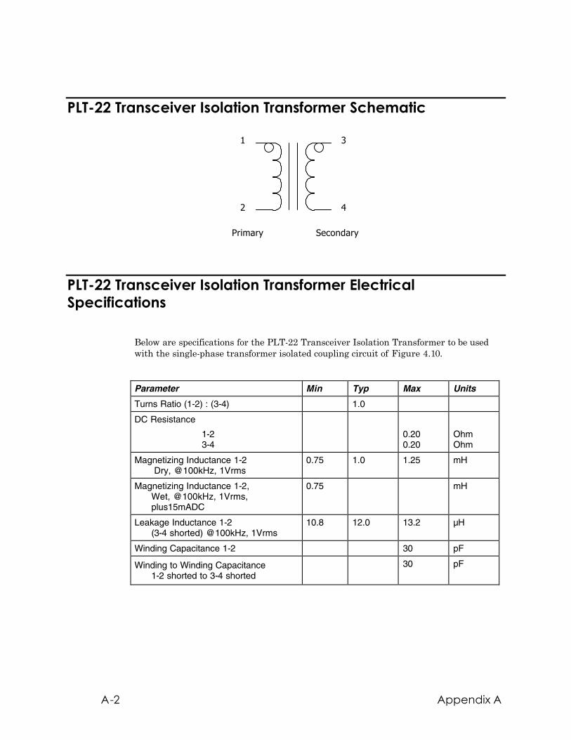
A-2 Appendix A
PLT-22 Transceiver Isolation Transformer Schematic
1
2
3
4
Primary Secondary
PLT-22 Transceiver Isolation Transformer Electrical Specifications
Below are specifications for the PLT-22 Transceiver Isolation Transformer to be used with the single-phase transformer isolated coupling circuit of Figure 4.10.
Parameter Min Typ Max Units
Turns Ratio (1-2) : (3-4) 1.0
DC Resistance
1-2 3-4
0.20 0.20
Ohm Ohm
Magnetizing Inductance 1-2 Dry, @100kHz, 1Vrms
0.75 1.0 1.25 mH
Magnetizing Inductance 1-2, Wet, @100kHz, 1Vrms, plus15mADC
0.75 mH
Leakage Inductance 1-2 (3-4 shorted) @100kHz, 1Vrms
10.8 12.0 13.2 µH
Winding Capacitance 1-2 30 pF
Winding to Winding Capacitance 1-2 shorted to 3-4 shorted
30 pF

LONWORKS PLT-22 in European Utility Applications A-3
PLT-22 Transceiver Isolation Transformer Vendors Contact vendors for details on operating temperature ranges, storage temperature ranges, safety agency compliance, mechanical design information, and pricing. Vendor Part Number Contact Instructions
Precision Components, Inc. 125 E. Lake Street, Suite 305 Bloomingdale, Illinois 60481
0505-0671 Telephone: +1-708-980-6448
Fax: +1-708-980-6485
EXCEL Electric Corporation 6501 N.W. 13th Court Plantation, Florida 33313
EXL-165 Telephone: +1-954-581-2330
Fax: +1-954-581-2355
Transpower Technologies, Inc. P.O. Box 187 Crystal Bay, Nevada 89402
TTI7143 Telephone: +1-702-831-0140
Fax: +1-702-831-3521

A-4 Appendix A
LONWORKS PLT-22 in European Utility Applications B-1
Appendix B
Three Phase Isolation Transformer Specifications
This appendix provides a schematic, specifications and supplier information for the PLT-22 transceiver isolation transformer with 1µH of series leakage inductance.

B-2 Appendix B
PLT-22 Transceiver Isolation Transformer Schematic
1
2
3
4
Primary Secondary
PLT-22 Transceiver Isolation Transformer Electrical Specifications
Below are specifications for the PLT-22 Transceiver Isolation Transformer to be used with the three-phase transformer isolated coupling circuit of Figure 4.12.
Parameter Min Typ Max Units
Turns Ratio (1-2) : (3-4) 1.0
DC Resistance
1-2 3-4
0.50 0.50
Ohm Ohm
Magnetizing Inductance 1-2 Dry, @100kHz, 1Vrms
1.1 1.8 mH
Magnetizing Inductance 1-2, 3-4 Wet, @100kHz, 1Vrms, plus 45mADC
1.0 mH
Leakage Inductance 1-2 (3-4 shorted) @100kHz, 1Vrms
1.0 µH
Winding Capacitance 1-2 25 pF
Winding to Winding Capacitance 1-2 shorted to 3-4 shorted
50 pF

LONWORKS PLT-22 in European Utility Applications B-3
PLT-22 Transceiver Isolation Transformer Vendors Contact vendors for details on operating temperature ranges, storage temperature ranges, safety agency compliance, mechanical design information, and pricing. Vendor Part Number Contact Instructions
Precision Components, Inc. 125 E. Lake Street, Suite 305 Bloomingdale, Illinois 60481
0505-0569 Telephone: +1-708-980-6448
Fax: +1-708-980-6485

B-4 Appendix B

LONWORKS PLT-22 in European Utility Applications C-1
Appendix C
PLT-22 Transceiver-Based Node Checklist
This appendix includes a checklist to ensure that products using the PLT-22 transceiver meet the specifications presented in this user’s guide.

C-2 Appendix C
PLT-22 Transceiver-based Node Checklist
PLT-22 Transceiver and Neuron Chip Connections
Item Check When Completed
Description
1 Transceiver pins connected as shown in table 2.1. 2 Environmental and electrical specifications shown in table 2.2
and figure 2.2. 3 6.5536 MHz parallel resonant crystal with a load capacitance
rating of 16 pF is connected to the PLT-22 transceiver. 4 Clock frequency measured to be 6.5536MHz ±200ppm
(including allowance for temperature variation). 5 The recommended number and placement of 0.1µF bypass
capacitors are near the Neuron Chip. See the Neuron Chip Data Book from Toshiba, Motorola, or Cypress.
6 The Neuron Chip input clock is ≥2.5MHz. 7 The traces connecting the crystal to the transceiver are not
greater than 20mm (0.8") in length. 8 External 120µF [minimum] 16VDC, aluminum electrolytic,
low-ESR [<0.3Ω @ 100kHz] VA capacitor is used. The capacitor must be exactly 16VDC (no higher or lower) to meet surge suppression levels. Verify suitable capacitor lifetime rating.
9 VA bypass capacitor is placed as close as possible to the transceiver with low-impedance ground and supply traces between the PLT-22 transceiver and the capacitor.
10 The three transceiver ground pins are connected with low-impedance traces, or a ground plane, between the transceiver and the Neuron Chip.
11 If used, the transceiver BIU and PKD are connected to low-current (≤8mA) LEDs via series current-limiting resistor connected to ground.
12 The BIU and PKD signals are connected to ESD protection diodes if a plastic or metal enclosure without a good ground connection is used.
13 The Neuron Chip CP3 pin is not connected and is left floating.
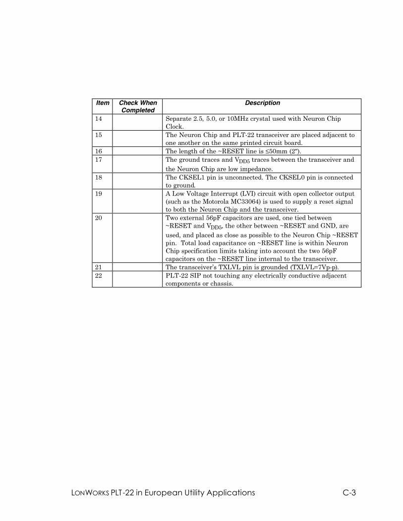
LONWORKS PLT-22 in European Utility Applications C-3
Item Check When Completed
Description
14 Separate 2.5, 5.0, or 10MHz crystal used with Neuron Chip Clock.
15 The Neuron Chip and PLT-22 transceiver are placed adjacent to one another on the same printed circuit board.
16 The length of the ~RESET line is ≤50mm (2"). 17 The ground traces and VDD5 traces between the transceiver and
the Neuron Chip are low impedance. 18 The CKSEL1 pin is unconnected. The CKSEL0 pin is connected
to ground. 19 A Low Voltage Interrupt (LVI) circuit with open collector output
(such as the Motorola MC33064) is used to supply a reset signal to both the Neuron Chip and the transceiver.
20 Two external 56pF capacitors are used, one tied between ~RESET and VDD5, the other between ~RESET and GND, are used, and placed as close as possible to the Neuron Chip ~RESET pin. Total load capacitance on ~RESET line is within Neuron Chip specification limits taking into account the two 56pF capacitors on the ~RESET line internal to the transceiver.
21 The transceiver’s TXLVL pin is grounded (TXLVL=7Vp-p). 22 PLT-22 SIP not touching any electrically conductive adjacent
components or chassis.
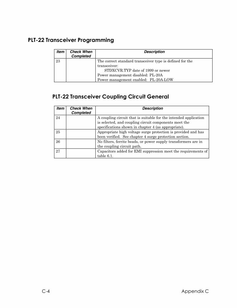
C-4 Appendix C
PLT-22 Transceiver Programming
Item Check When Completed
Description
23 The correct standard transceiver type is defined for the transceiver: STDXCVR.TYP date of 1999 or newer Power management disabled: PL-20A Power management enabled: PL-20A-LOW
PLT-22 Transceiver Coupling Circuit General
Item Check When Completed
Description
24 A coupling circuit that is suitable for the intended application is selected, and coupling circuit components meet the specifications shown in chapter 4 (as appropriate).
25 Appropriate high voltage surge protection is provided and has been verified. See chapter 4 surge protection section.
26 No filters, ferrite beads, or power supply transformers are in the coupling circuit path.
27 Capacitors added for EMI suppression meet the requirements of table 6.1.
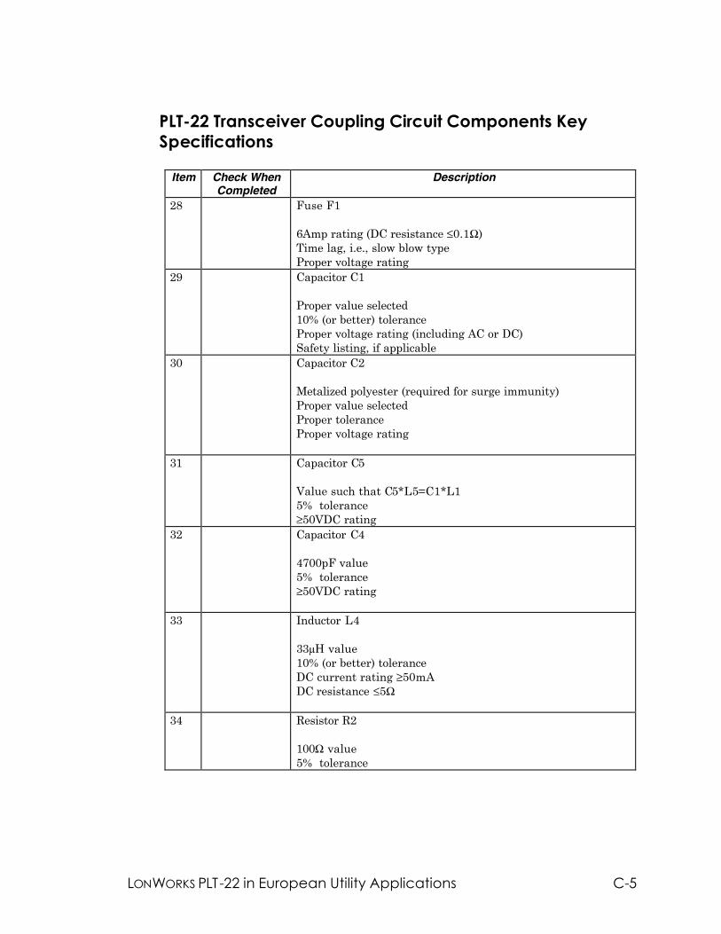
LONWORKS PLT-22 in European Utility Applications C-5
PLT-22 Transceiver Coupling Circuit Components Key Specifications
Item Check When
Completed Description
28 Fuse F1 6Amp rating (DC resistance ≤0.1Ω) Time lag, i.e., slow blow type Proper voltage rating
29 Capacitor C1 Proper value selected 10% (or better) tolerance Proper voltage rating (including AC or DC) Safety listing, if applicable
30 Capacitor C2 Metalized polyester (required for surge immunity) Proper value selected Proper tolerance Proper voltage rating
31 Capacitor C5 Value such that C5*L5=C1*L1 5% tolerance ≥50VDC rating
32 Capacitor C4 4700pF value 5% tolerance ≥50VDC rating
33 Inductor L4 33µH value 10% (or better) tolerance DC current rating ≥50mA DC resistance ≤5Ω
34 Resistor R2 100Ω value 5% tolerance
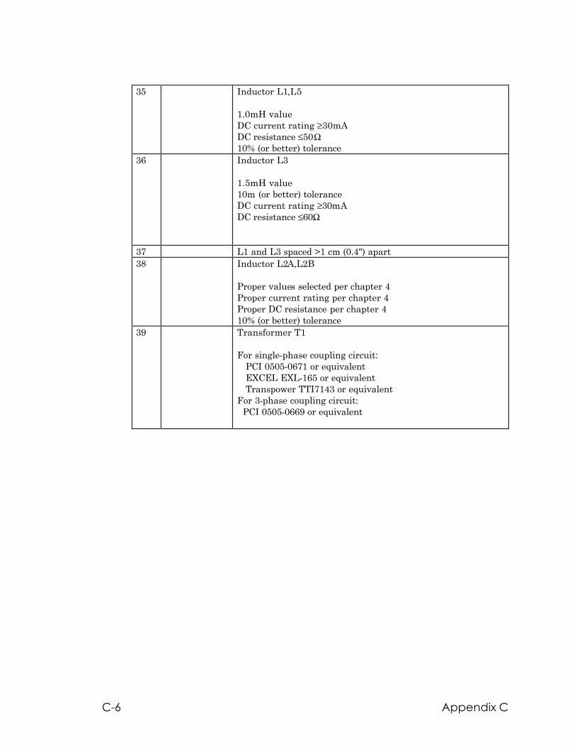
C-6 Appendix C
35 Inductor L1,L5 1.0mH value DC current rating ≥30mA DC resistance ≤50Ω 10% (or better) tolerance
36 Inductor L3 1.5mH value 10m (or better) tolerance DC current rating ≥30mA DC resistance ≤60Ω
37 L1 and L3 spaced >1 cm (0.4") apart 38 Inductor L2A,L2B
Proper values selected per chapter 4 Proper current rating per chapter 4 Proper DC resistance per chapter 4 10% (or better) tolerance
39 Transformer T1 For single-phase coupling circuit: PCI 0505-0671 or equivalent EXCEL EXL-165 or equivalent Transpower TTI7143 or equivalent For 3-phase coupling circuit: PCI 0505-0669 or equivalent
LONWORKS PLT-22 in European Utility Applications C-7
Item Check When Completed
Description
40 Resistor R1 Proper value for discharge time requirements Proper voltage rating (>1.4*ACRMS line voltage)
41 Resistor R3 Value of 82Ω minus L5 DC resistance
42 Varistor RV1 Proper AC or DC voltage rating so as not to clamp AC peaks Surge rating for application requirements, see chapter 4
43 Diode D1 1N4935 type
PLT-22 Transceiver Power Supply - General
Item Check When Completed
Description
44 If a linear supply has been used skip the remaining power supply check list sections.
PLT-22 Transceiver Power Supply - Switching Type
Item Check When Completed
Description
45 The preferred operating frequency of the switching power supply is either 95kHz - 110kHz or >140kHz under all line, load, environmental, and production conditions.
46 A series inductor is used between the power supply input and the power mains communication channel to avoid attenuation due to the input stage of a switching power supply.
47 The value of the series inductor has been selected for the application requirements as described in chapter 5.
48 The inductor has a current rating adequate to support the peak currents drawn by the power supply without saturation.
C-8 Appendix C
Item Check When Completed
Description
49 The LC resonant frequency of the inductor is at least 1 octave from the communication frequency range (70kHz-95kHz) when the inductor is combined with the input capacitance of the switching supply.
50 The power supply complies with the input noise masks shown in chapter 5.
51 Measurements of the power supply are made by connecting the supply to the artificial mains network as specified in subclause 8.2.1 of CISPR Publication 16, second edition. Measurements are made over the full range of anticipated loads on the supply and conducted in accordance with CENELEC EN 50065-1 measurement standards with measurement bandwidths of 200Hz below 150kHz and 9kHz above 150kHz, as described in CISPR 16.
52 If the power supply does not meet the appropriate noise mask for the power supply input, a correct filter is installed between the local switching power supply and the power line.
53 All output noise "masks" shown in chapter 5 are satisfied using measurements taken over the full range of anticipated loads on the supply.
EMI & ESD Design
Item Check When Completed
Description
54 The “leakage” capacitance from high frequency circuit traces is controlled via guard traces.
55 The product's package is designed to minimize the possibility of ESD hits arcing into the node's circuit board. If the product's package is plastic, then the PCB is supported in the package so that unprotected circuitry on the PCB is not adjacent to any seams in the package. The PCB is not touching the plastic enclosure near a seam.
56 Explicit clamping of user-accessible circuitry is used to shunt ESD currents from that circuitry to the center of the star ground on the PCB.
57 The connector, diodes and decoupling capacitor are all located close to the center of the star ground.
LONWORKS PLT-22 in European Utility Applications C-9
Product Qualification - EMC
Item Check When Completed
Description
58 Proper measurement of conducted emissions is used to verify compliance with CENELEC EN 50065-1 as described in chapter 5.
59 A 50Ω//(50µH+5Ω) Line Impedance Stabilization Network (LISN) as specified in CISPR Publication 16, second edition is used for measurement.
60 The appropriate attenuator is used to ensure that the transceiver's transmit signal does not overload the measurement apparatus. The residual noise floor of the entire measurement set is verified to be at least 10dB below the specification limit (a noise floor less than 36dBµV for CENELEC EN 50065-1 measurements).
61 Measurements are made with a quasi-peak detector and the average detector as specified in CISPR Publication 16.
62 The CENELEC EN 50065-1 measurements are made with a 200Hz bandwidth filter for measurements below 150kHz, and a 9kHz bandwidth filter for measurements above 150kHz.
63 For EN50065-1 verification all testing is done with a Rohde&Schwarz EMI Test Receiver ESHS30 (or equivalent tester with proper filter skirts) set to manual mode using a set-up program described in chapter 5. Alternatively, Hewlett Packard equipment is used with an appropriate external filter.
Product Qualification - Electromagnetic Immunity and Communication Performance
Item Check When
Completed Description
64 The product is tested to appropriate levels of either CEI/IEC 1000-4-5, or IEEE C62.41-1991.
65 The product is verified to meet communication performance capabilities per chapter 7.

C-10 Appendix C