Embed Size (px)
Citation preview
VACUUM CHALLENGES AND SOLUTIONS
In association with Practical Vacuum
October 2004
Step
hen
Kill,
Ruth
erfo
rd A
pple
ton
Labo
rato
ry

3
INTEGRAMDeep Dry Etch Service
For your MEMS projects, you cannow access a state-of-the-artdeep reactive ion etch clustertool (STS ASPECT).
We can process 100, 125,150mm wafer sizes.
Bulk silicon or SOI wafers.
Feature size: 2µm to severalmm with aspect ratios up to30:1.
Contact us for prices andfurther information
Tel: +44(0) 1684 896262email: [email protected]
Vacuum challengesand solutionsThis is the third year in a row that Physics World has published a specialsupplement on vacuum science and technology. Once again, the vacuumindustry is thriving with ideas and innovation. As always the role of thesemiconductor industry is central. The global market for vacuum pumpsand gauges for the semiconductor and flat-panel display industries isworth $1.5bn – an increase of 38% on last year – and is projected to growto $2.2bn in 2009, albeit after a cyclical dip in 2006/7 (p5). Elsewhere,new research facilities – like Diamond (p9), the new synchrotron radia-tion source being built in the UK – are investing heavily in vacuumequipment and expertise, and there are also exciting new developmentsin components and systems, such as ceramic-to-metal seals (p11), non-evaporable getters (p15), residual gas analysers (p17) and MBEmachines (p19). And for people who are new to the vacuum field, or per-haps not as up to date as they would like to be, the supplement also con-tains articles on relevant training courses (p7) and books (p21).
ContentsVacuum systems go for growth 5The manufacture of semiconductor components and flat-panel displays presents challengesand opportunities for the vacuum industry. Bob Mariner of VLSI Research Europe reports
What to look for in vacuum training 7Training in vacuum science and technology is available from a number of different sources,as Rick Spencer of Alacritas Consultancy describes
Future looks bright for vacuum at Diamond 9How do you design the vacuum system for the biggest science project to be built in the UK inmore than a decade? Matthew Cox of the Diamond Light Source explains
Ceramics show their mettle 11Ceramic-to-metal seals play a crucial role in modern vacuum systems, as Jason Bodson ofInsulator Seal reveals
NEG pumps can go to the extremes 15Non-evaporable getters are making an impact in both research and industrial applications.Paolo Manini of the SAES Getters Group reports on progress
Spectrometry sets the pace in process control 17Quadrupole mass spectrometry is being used for a variety of applications across thesemiconductor industry, as Peter Hatton of Hiden Analytical describes
MBE lays foundations for spintronics 19Molecular beam epitaxy places enormous demands on vacuum systems. Richard Campionof Nottingham University outlines the challenges
Variety of books can fill the vacuum 21Looking for the best vacuum book? Philip Danielson of The Vacuum Lab offers some advice
Diary 22©2004 IOP Physics Publishing Ltd. All rights reserved.
Dirac House, Temple Back, Bristol BS1 6BE, UK.
V A C U U M C H A L L E N G E S A N D S O L U T I O N S O C T O B E R 2 0 0 4

Veeco Anode Layer Ion Sources:The confident choice for larger-area coatings.
Veeco’s anode layer ion sources take high-quality, high-performance coatingsand supersize them. Now, you can get ion beam advantages in your largestindustrial processes, at today’s accelerated line speeds. With lengths to 4 metersand militorr operational pressures, Veeco’s ALS sources have taken ion sources out of the cleanroom and into the factory. The advantages just get larger when you consider Veeco is the world’s largest ion source supplier, with a morededicated investment in R&D, more production facilities and more worldwide support than any other ion source manufacturer.
Broadest Line.Greatest Worldwide Reach.Biggest Commitment.
Visit us at www.veeco.com/ALSor call us for more information at:Cambridge, UK Int + 44 (0)1954 233900Dourdan, F Int + 33 (0)1645 93520Mannheim, D Int + 49 (0)6218 42100Breda, NL Int + 31 (0)7652 44850
5V A C U U M C H A L L E N G E S A N D S O L U T I O N S O C T O B E R 2 0 0 4
The manufacture of semiconductorcomponents and flat-panel displayspresents major technologicalchallenges to the vacuum equipmentindustry. Bob Mariner reports
The size of structures that now need to be produced to con-struct a semiconductor chip are measured in tens of nano-metres, and film thicknesses may be just a few atomic layers.The integrated circuit industry is well and truly in the era ofnanotechnology, so processes must be controlled to unprece-dented levels. A single point of contamination, even if it ismuch less than 1 µm across, can be devastating to the functionof the circuit at the point where it lands. Bearing in mind that asingle semiconductor chip may be built up from several hun-dred million individual transistors, it is easy to see how criticalit is to control contamination within the vacuum system.
Similarly, control of the vacuum is just one of many criticalprocesses that are needed to produce nanoscale structures. Theproduct being processed is likely to have a very high value, soreliability of the process tools is paramount: a single systemfailure could result in the destruction of material worth tens ofthousands or even millions of dollars. Additionally there is thecost of lost production during system downtime. The gasesused in these processes are often very corrosive, or they may beinclined to leave deposits within the pumping system, but thepumps must operate reliably in a 24/7 environment.
The critical nature of these vacuum processing systemsmeans that the associated vacuum subsystems, such as pumpsand gauges, have a high value. A recent report from VLSIResearch values the market for vacuum pumps and gaugesused in semiconductor, flat-panel display and related manu-facturing at $1.5bn in 2004, an increase of 38% on 2003. Aftera cyclical dip in 2006/7, this market is projected to reach avalue of $2.2bn in 2009. The semiconductor industry is notori-ously cyclical, and the demand for production equipment maygrow more than 70% in a year, as in 2000, or fall more than30%, as in 2001. This is a challenging business environment tomanage from the operations and the technology perspective.
The production of semiconductor components is changing,with the diameter of the silicon wafers increasing from200 mm to 300 mm. This means larger process chambers arerequired, putting greater demands on the vacuum systems.Some 21 fabrication plants around the world are currentlyramping up production of 300 mm wafers, with another 11scheduled to begin production in 2005. Integrated circuits pro-duced in these new factories utilize new materials to stretchelectronic performance, and many of these require new andcomplex processes. Atomic layer deposition and strained sili-con are two new process techniques now entering production.High-k and low-k dielectric materials must be deposited toenhance electronic performance, while copper interconnects
are rapidly replacing the conventional aluminium approach.Although the market for flat-panel display manufacturing
systems is much smaller than that for semiconductors compo-nents, the technology brings its own unique challenges. Newfactories are now being built for Generation-6 glass panels,and Generation-7 factories (which process glass panels meas-uring 1.8 ×2.1 m) will soon start construction. Such massivevacuum process chambers place their own special demands onthe vacuum subsystems.
About 55% of the vacuum-pump market within the semi-conductor and related industries is for dry pumps, 33% for tur-bomolecular pumps and 12% for cryogenic pumps, and thisproduct mix is unlikely to change much in the future. BOCEdwards is the largest pump supplier, followed by Leybold,Alcatel (adiXen) and Ebara, while Helix Technology is thelargest supplier of cryogenic pumps.
The market for vacuum gauges is being pushed to muchhigher accuracies and greater measurement ranges, which isadding to complexity and cost. Here the leading suppliers areHelix Technology, Inficon and MKS Instruments.
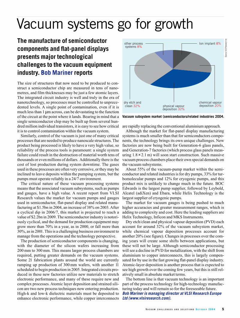
Dry etch/clean and physical vapour deposition (PVD) eachaccount for around 32% of the vacuum subsystem market,while chemical vapour deposition processes account foranother 20% (see figure). Changes in processes over the com-ing years will create some shifts between applications, butthese will not be large. Although semiconductor processingwill see a decline in PVD for metallization, with the shift fromaluminium to copper interconnects, this is largely compen-sated for by use in the fast growing flat-panel display industry.Atomic-layer deposition is another process that is expected tosee high growth over the coming few years, but this is still rel-atively small in absolute market terms.
The bottom line is that vacuum technology is an importantpart of the process technology for high-technology manufac-turing today and will remain so for the foreseeable future.Bob Mariner is managing director at VLSI Research EuropeLtd (www.vlsiresearch.com).
Vacuum systems go for growthIon implant 8%
chemical vapourdeposition 20%
dry etch andclean 32% physical vapour
deposition 32%
other processsystems 8%
Vacuum subsystem market (semiconductors/related industries 2004.
Sour
ce:V
LSI R
esea
rch
Inc

www.alacritas.net
Expertise in thin films & vacuum
processing
Technical adviceand support
Training for vacuum and vacuum coating
Technical authors
Agents for :-
Advanced ConvertersSputter power supplies
BOC IntellemetricsControl of thickness and etch depth
Hiden AnalyticalMass and energy analysers
Call Rick Spencer on 01530 244655email : [email protected]
Creative Group is one of Europe's leading specialists in
vacuum technology and manufactures an extensive range of
quality fittings, instrumentation, pumps and systems. Creative
also provides metal joining, inspection, design and vacuum
testing services to many leading names in the process,
research, semiconductor and aerospace industries.
Creative Group
Cavea House, Decoy Road, Worthing
West Sussex BN14 8ND UK.
Tel:+44(0)1903 204 542
Fax:+44(0)1903 215 678
E-mail: [email protected]
www.creativevacuum.co.uk
Creative GroupVacuum Technology Solutions
Design to Production
KF, ISO and CF vacuum fittings
Stainless steel bellows and flexible hoses
Vacuum gauges and switches
Valves, diaphragms and pressure sensitive elements
Plant, rigs and reservoirs
Electron beam and TIG welding
Vacuum brazing and heat treatment

7V A C U U M C H A L L E N G E S A N D S O L U T I O N S O C T O B E R 2 0 0 4
Many people become involved with vacuum processes whileworking on something else. The vacuum is just a tool toachieve what they really want, which could be the efficientproduction of something in industry or the development of anew device in a university research lab. The focus of attentionis usually on this main aim while the vacuum is forgotten.
However, to get the best of anything you need to know howit works and what its limitations are. For example, when usinga vacuum it is best to know which impurities will be present inyour vacuum; how to get the best vacuum; how good a vacuumyou actually need; how to make the most of the expensive vac-uum equipment that you just bought; whether to believe theclaims of the supplier who is trying to sell you their latest pieceof kit; and why the vacuum process that worked yesterday sud-denly doesn’t work today.
Training in vacuum is thus very useful (often essential) to getthe best out of existing vacuum equipment or to design andspecify new equipment. Having decided that training in vac-uum and vacuum technology would be useful, there are threemain sources of vacuum training available: on-line training;short (1–3 day) courses; and academic qualifications.
Whatever your needs, you should be able to find the rightcourse for you from one of the organizations listed in the box.Rick Spencer runs Alacritas Consultancy Ltd(www.alacritas.net).
What to look for in vacuum training
Alacritas Consultancy (www.alacritas.net) On-site shortcourses in vacuum technology and vacuum coating.BOC Edwards (www.training.bocedwards.com) Short courses invacuum technology at the Edwards Training Centre in Crawley.Leybold Vacuum UK (www.leyboldvac.de/uk/news/training_ufr.html) Short courses in vacuum technology at Leybold or on-site.Low-pressure.com (www.low-pressure.com) On-site shortcourses in vacuum technology.Queen's University of Belfast (www.plasmavacuum.net) On-line courses in plasma and vacuum technology, possiblyleading to an MSc or graduate diploma.Salford University (www.salford.ac.uk/course-finder/course/1385) MSc or postgraduate diploma in vacuum engineeringand applications.VacuumCoatingTraining.com (www.VacuumCoatingTraining.com) On-line training in vacuum technology and vacuumcoating.Willett Technical Services (www.vacuumtraining.co.uk) On-site short courses in vacuum technology.York University (www.york.ac.uk/depts/phys/lectures/vactech.htm) Short course in vacuum technology.
Training in vacuum technology

The leading publication in compound semiconductors
Subscribe FREE OF CHARGEIf you have enjoyed reading this issue of Compound Semiconductor and you are not alreadya subscriber, why not subscribe online now by visiting compoundsemiconductor.net/subscribe.
It will only take a few moments of your time, and means that you will soonbegin receiving your own personal copy of the magazine.

9V A C U U M C H A L L E N G E S A N D S O L U T I O N S O C T O B E R 2 0 0 4
The vacuum system for the DiamondLight Source is designed to maximizethe scientific return from this leading-edge facility, as Matthew Cox explainsDiamond is a third-generation synchrotron light source that iscurrently being constructed on the Chilton/Harwell sciencecampus near Oxford in the UK. Radiation from the source –the biggest science project to be built in the UK in more than adecade – will be used in a range of experiments in the life,environmental and physical sciences. The success of theseexperiments will depend on the quality of the radiation gener-ated by the source, which in turn will depend on many factors,including the quality of Diamond’s vacuum systems.
At the heart of Diamond is a storage ring with a circumfer-ence of 561 m, around which electrons with energies of 3 GeVcirculate. Magnetic insertion devices known as undulatorsgenerate high-brightness X-rays with photon energies of up to20 keV, while other devices known as multipole wigglers pro-duce high-flux beams with energies of up to 100 keV.
Diamond is currently in the detailed design, build and pro-curement phase. Stage 1 of the building work, which includedsite preparation and foundations, was completed in September2003, and work on the buildings and accelerator enclosures isnow under way. The Diamond organization currently employs150 staff and will eventually grow to some 300.
The first seven beamlines are due to start operations in 2007,with an additional 15 beamlines being constructed at a rate of4–5 per year from 2007 onwards. The electrons will be accel-erated in a linear accelerator and a booster, before being trans-ferred to the main storage ring, and the areas that will housethese two devices have recently been completed. The inner andratchet walls of the storage ring tunnel are nearing completion,and Diamond’s technical services building, which houses themain plant rooms, is also well under way.
Within the storage ring, electrons will gradually be lost fromthe beam as a result of collisions with other electrons or withany stray gas molecules left in the ring after it has been evacu-ated. To minimize beam–gas interactions and to achieve a highstored beam lifetime, the storage ring will operate in the ultra-high vacuum pressure region. In addition to the normal ther-mal desorption processes, gas molecules are also kicked offthe walls of the vessel by the synchrotron light. This meansthat the dynamic pressure during operation can be many timeshigher than the static pressure with no stored beam. The targetfor Diamond is to achieve a dynamic pressure of 10–9 mbar
with 300 mA stored current after a period of beam condition-ing. This should result in a beam lifetime of at least 10 hours forusers of the facility.
Most of the hundreds of kilowatts of synchrotron light willbe absorbed by water-cooled copper absorbers mounted in thevacuum vessels. As synchrotron radiation can also heat thevacuum chambers, the walls of the vacuum vessel will bemade of stainless steel, and will include further water-cooledstrips of copper located at critical positions to absorb the radi-ation. Owing to the tight mechanical tolerances needed,e-beam welding will be used extensively in vessel construc-tion. Extruded aluminium will also be used for some of thevessels that house the insertion devices.
The storage ring will be pumped by 500 maintenance-freeion pumps, which were chosen for long-term reliability andstability. Vacuum quality will be monitored by 200 invertedmagnetron cold cathode gauges and 72 quadrupole residualgas analysers.
The storage ring will be constructed and installed in 24 sec-tions, each comprising an arc section and a straight section.Each arc section will consist of three girders, each of which inturn will be fitted with a string of vacuum vessels 6–7 m inlength. As there is no in situ bake-out, these will be assembled,pre-baked and installed under vacuum.
From section to section, vacuum vessels and equipment thatare installed on each corresponding girder will be identical. Ifa vacuum vessel needs to be maintained or repaired once thesynchrotron has started operations, a complete girder assem-bly will be removed and replaced by a preconditioned assem-bly that will be on standby. This will allow the repairs to goahead with minimal impact on the experiments taking place onany of the beamlines. Matthew Cox is head of the vacuum group for the DiamondLight Source (www.diamond.ac.uk).
Future looksbright for vacuumat Diamond
The Diamond Light Source will use advanced vacuum techniques.
Step
hen
Kill,
Ruth
erfo
rd A
pple
ton
Labo
rato
ry

w w w . s p e l l m a n h v . c o m
475 Wireless Blvd.Hauppauge, NY 11788 USA
tel: +1-631-630-3000fax: +1-631-435-1620
Spellman Japan3-15 Kanayama-cho,Kawaguchi shiKawaguchi-shiSaitama-ken, Japan 332-0014tel: +81(0) 48-228-3222fax: +81(0) 48-228-3224
Spellman SIP LtdBlock B #06-05/06,No. 5 Xinghan StreetNo 5 Xinghan StreetSuzhou Industrial Park, China, 215021tel: +86(0) 512-67630010 fax: +86(0) 512-67630030
Spellman de MexicoDiagonal Lorenzo de la Garza no. 65H. Matamoros, TamaulipasH Matamoros TamaulipasMexico
Spellman Ltd.Broomers ParkBroomers Hill Lane PulboroughBroomers Hill Lane PulboroughUnited Kingdomtel: +44(0) 1798 877000fax: +44(0) 1798 872479
• Over 50 Years of High Voltage Innovation• Custom Designed Solutions for Your Applications• World-Class ISO Certified Production Facilities•• Global Sales and Service •
Spellman High Voltage is your resource for E-Beam and I-Beam applications
where ultra-high stability and precisionare paramount. For E-Beam Lithography,
Scanning Electron Microscope,Focused Ion Beam and SemiconductorMetrology systems, you can depend on
Spellman's innovation and custom designcapability to provide the precise solution for your requirements. Contact our application specialists
for more information on our FIB/EBM/EGM family of high voltage generators. Call +1-631-630-3000 or
email: [email protected]
EGM SERIES- For use in E-Beam Lithography Systems- Beam Stability <2.5ppm per 12 hrs Constant Operation- Active Bias System
EBM SERIES- Triode Modulefor drivingE-Beam Columns
- High Precision,Low Noise, Ultra-Stable
- For use in SEMs
FIB SERIES- Specifically designed forFocused Ion Beam Applications
- Integrated multiple floatingoutputs with opticallyisolated controls
- High Stability, Very Low Ripple

11V A C U U M S U P P L E M E N T O C T O B E R 2 0 0 4
Ceramics are crucial materials for modern vacuum equipmentcomponents. This is particularly true for the viewports thatallow us to see what is happening inside the vacuum chamberand the feedthroughs that connect instrumentation or machin-ery inside the chamber to external control, monitoring and-power-supply equipment. Viewports are made of inorganicglasses or single crystals, while polycrystalline aluminiumoxide is the primary insulator used to isolate high-voltage, high-power and low-power signal transfer lines in feedthroughs.
Obviously the seals between the vacuum chamber, which ismade of metal, and these ceramic components need to be of thehighest quality. Moreover, the ceramic components must with-stand bake-out temperatures of up to 450 °C without disruptingthe vacuum environment. Ceramic-to-metal seals are madeusing a ductile brazing alloy between the ceramic and a low-expansion metal alloy. Incorporation of an oxygen-activemetal, together with careful control of the surface characteris-tics and the firing environment, allows the braze alloy to wetand react with the ceramic, producing an intimate chemicalbond. The seals produced with this technology are vacuum-tight to better than 10–9 torr.
The biggest applications of these components are the thin-film deposition and etching techniques that are used in micro-electronics processing. Thin-film techniques are also used foroptical coatings and display technologies. Analytical instru-ments are another major application, including electron micro-
scopes, atomic and molecular spectrometers, and surfaceanalysis devices.
Vacuum feedthroughs can be made to suit practically anypurpose. Low-power data signals are transmitted throughmultipin, coaxial or special thermocouple feedthroughs.Insulator Seal, a division of MDC Vacuum Products Corpor-ation, builds high-voltage feedthroughs rated at up to 100 kVand high-current feedthroughs rated at up to 1000 A. Non-mag-netic, low-induction feedthroughs carry up to 35 kW of RFpower, which is commonly used for in-vacuum induction heat-ing. Simple “breaks” provide electrical isolation of chambersor components.
On the optical side, fibre-optic feedthroughs transmit up to100 kW cm–2 of continuous-wave or 500 kW cm–2 of pulsepower. Meanwhile, vacuum viewports of virtually any opticalceramic can be made using our proprietary VacOptix technol-ogy. Such viewports are also well suited to corrosive, cryo-genic and ultrahigh-vacuum environments where extendedinfrared or ultraviolet transmission is desired.
Though not well known, ceramic-to-metal seals are vitalparts of the devices that have been responsible for countlessscientific discoveries and technological advances, and thathave made it possible to manufacture ever-more sophisticatedelectronic devices.Jason Bodson is a design engineer with Insulator Seal(www.insulatorseal.com).
Ceramics show their mettle
You and Varian: the Winning Team.
Have a test run!
Get the benefits of a global supplier of Vacuum Technology:• A pioneer in the vacuum industry for over 50 years• 24 hours Service Support available worldwide• Innovative Turbomolecular pump line with controllers on board• Full range of Diffusion, Rotary Vane and Scroll pumps• World leader in Ion Pumps technology• On-line ordering now available
www.varianinc.com/vacuum
Toll Free Number for United States
1 (800) 882 7426for Europe
00 800 234 234 00

6460 Parkland Drive,Sarasota, FL U.S.A. 34243
Toll-Free 1.800.548.9509Fax 1.941.751.3841
e-mail: [email protected]
Save 10% on your nextPurchase of High & UltraHigh Vacuum Products
www.insulatorseal.comwww.insulatorseal.com
Electrical & OpticalCeramic-To-Metal Vacuum Components

23842 Cabot BoulevardHayward, CA
U.S.A. 94545-1661Toll-Free 1.800.443.8817
Fax 1.510.887.0626e-mail: [email protected]
VACUUM PRODUCTS CORPORATION
www.mdcvacuum.comwww.mdcvacuum.com
Visit us online or Call for a Free Catalogue
Visit us online or Call for a Free Catalogue
Order direct from our factories and receive 10%off of our catalogue priceson MDC Flanges & Fittings,Valves, Roughing Components,Motion & Manipulation, Chambersand Thin Film Deposition products,as well as on ISI ElectricalFeedthroughs, Brakes & Envelopesand Sapphire & Quartz ViewportsLimited time offer
for Vacuum Scienceand Technology
Building-Blocks
Electron beamTechnology

High Quality Quartz Monitor CrystalsNew! Stress relieving Alloy Crystals designed specifically
for dielectric coating
Other products available from Scotech
• Ion Sources (RF & DC)• Electron Beam Guns & Power Supplies
• Magnetic Fluid Feedthroughs• RF & DC Power Supplies
• Evaporation Materials & Sputtering Targets• E Beam Crucible Liners
• Thermal Evaporation Sources
Scotech Limited, Nethermill Properties, Langbank, Renfrewshire, Scotland, UK, PA14 6YGTel +44 (0)1475 540689 Fax +44 (0)1475 540206
Email [email protected] Web www.scotech.ltd.uk
Equipment & Consumables for the Vacuum, Thin Filmand Semiconductor Industries
Email [email protected]
www.bocedwards.com
• No vacuum oil to change
• No grease or bearings in the vacuumenvironment
• Quick and easy to service
• Patented Bearing Shield design offersa totally dry solution
• Easily replace existing rotary pump on most LCMS systems – plug & play
ICPMS
GCMSFTMS
TOF
LCMS
XDS PUMP SERIES:
CONVERT TOTHE TOTALLY DRYSOLUTION!
01293 528844
NEVER CHANGE
THE OIL IN YOUR
VACUUM PUMP
AGAIN!
X D S R A N G E B E N E F I T S :
GOLD AND PLATINUMPRODUCTS FOR INDUSTRY,
RESEARCH AND TECHNOLOGYAs specialists in gold and platinum
products whatever your needs - however urgent - call +44 (0)121-766 6022.
We will be pleased to discuss your requirements.
BIRMINGHAM METALCOMPANY LIMITED
SPECIAL PRODUCTS DIVISIONGarrison Street, Bordesley,
Birmingham B9 4BNUK
Telephone: +44 (0) 121 766 6022Fax: +44 (0) 121 766 7485www.birminghammetal.com
Telephone: 001 775 885 6866Fax: 001 775 885 8835
FRANCETelephone: 00 33 (0) 2 3507 60 00
Fax: 00 33 (0) 2 3570 64 39
15V A C U U M C H A L L E N G E S A N D S O L U T I O N S O C T O B E R 2 0 0 4
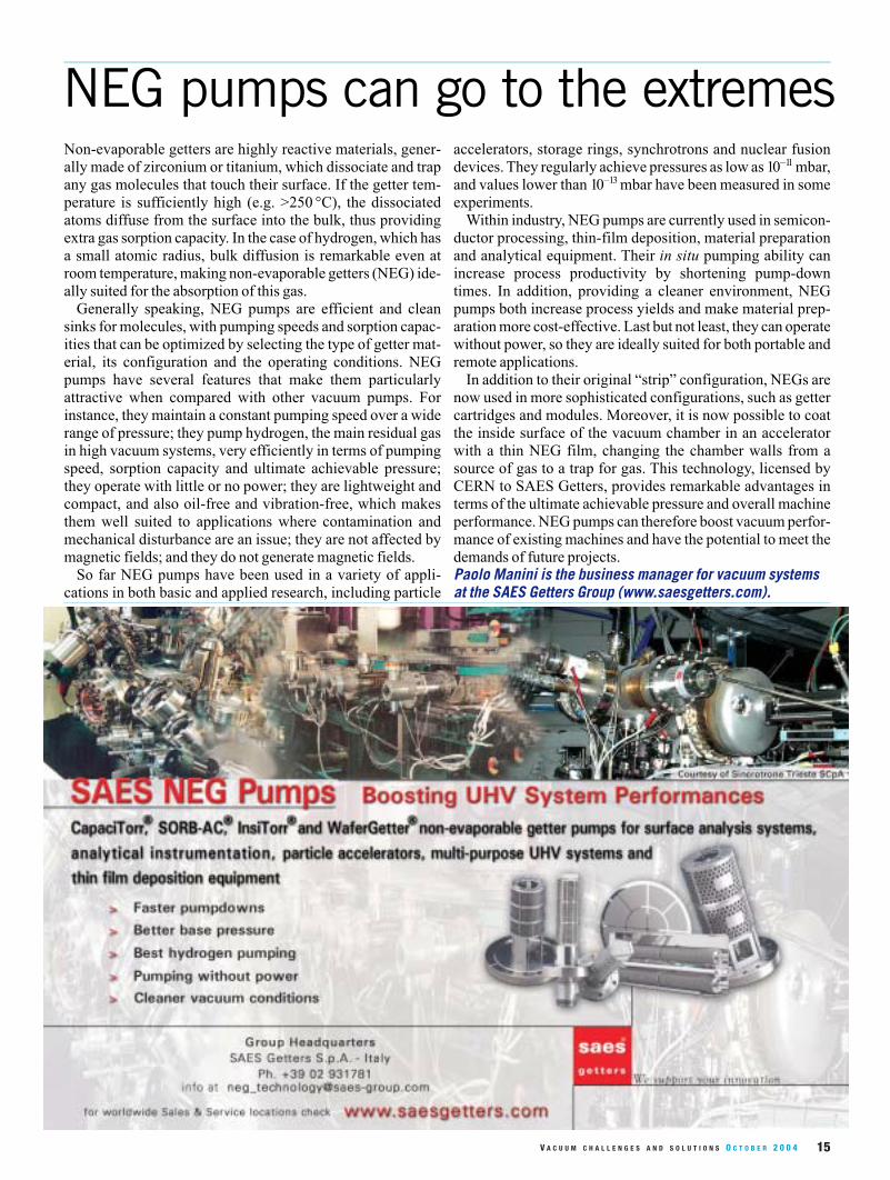
Non-evaporable getters are highly reactive materials, gener-ally made of zirconium or titanium, which dissociate and trapany gas molecules that touch their surface. If the getter tem-perature is sufficiently high (e.g. >250 °C), the dissociatedatoms diffuse from the surface into the bulk, thus providingextra gas sorption capacity. In the case of hydrogen, which hasa small atomic radius, bulk diffusion is remarkable even atroom temperature, making non-evaporable getters (NEG) ide-ally suited for the absorption of this gas.
Generally speaking, NEG pumps are efficient and cleansinks for molecules, with pumping speeds and sorption capac-ities that can be optimized by selecting the type of getter mat-erial, its configuration and the operating conditions. NEGpumps have several features that make them particularlyattractive when compared with other vacuum pumps. Forinstance, they maintain a constant pumping speed over a widerange of pressure; they pump hydrogen, the main residual gasin high vacuum systems, very efficiently in terms of pumpingspeed, sorption capacity and ultimate achievable pressure;they operate with little or no power; they are lightweight andcompact, and also oil-free and vibration-free, which makesthem well suited to applications where contamination andmechanical disturbance are an issue; they are not affected bymagnetic fields; and they do not generate magnetic fields.
So far NEG pumps have been used in a variety of appli-cations in both basic and applied research, including particle
accelerators, storage rings, synchrotrons and nuclear fusiondevices. They regularly achieve pressures as low as 10–11 mbar,and values lower than 10–13 mbar have been measured in someexperiments.
Within industry, NEG pumps are currently used in semicon-ductor processing, thin-film deposition, material preparationand analytical equipment. Their in situ pumping ability canincrease process productivity by shortening pump-downtimes. In addition, providing a cleaner environment, NEGpumps both increase process yields and make material prep-aration more cost-effective. Last but not least, they can operatewithout power, so they are ideally suited for both portable andremote applications.
In addition to their original “strip” configuration, NEGs arenow used in more sophisticated configurations, such as gettercartridges and modules. Moreover, it is now possible to coatthe inside surface of the vacuum chamber in an acceleratorwith a thin NEG film, changing the chamber walls from asource of gas to a trap for gas. This technology, licensed byCERN to SAES Getters, provides remarkable advantages interms of the ultimate achievable pressure and overall machineperformance. NEG pumps can therefore boost vacuum perfor-mance of existing machines and have the potential to meet thedemands of future projects.Paolo Manini is the business manager for vacuum systemsat the SAES Getters Group (www.saesgetters.com).
NEG pumps can go to the extremes

FO
R
WORLDWIDE CON
TAC
T:
PrecisionSurface Science
High resolution, fast response,analysis of gases, radicals and ions in:
• UHV Desorption Studies• End Point Detection• Surface/Interface Analysis• SIMS/ISS/SNMS• Molecular
BeamExperiments
High resolution, fast response,analysis of gases, radicals and ions in:
• UHV Desorption Studies• End Point Detection• Surface/Interface Analysis• SIMS/ISS/SNMS• Molecular
BeamExperiments
Instruments for Exact Science
E-mail: [email protected] EQS SIMS Probes

17V A C U U M S U P P L E M E N T O C T O B E R 2 0 0 4
Semiconductor fabrication involves a range of vacuum, gasand plasma processes, and all of these require developmentand monitoring to maintain and increase production yields.Mass spectrometry offers unrivalled specificity and sensitivityfor the analysis of gases and vapours, with quadrupole massspectrometry delivering the benefits of the technique in a com-pact and easy-to-use package.
Many readers will be familiar with the residual gas analyser(RGA) that measures the partial pressure of species in high-vacuum and ultrahigh-vacuum processing environments. Thedevice is now in common use across the semiconductor indus-try, from the ion-implant stage through to the deposition andetching process steps. The RGAprovides users with a windowinto their processing environment, identifying contaminationlevels, diagnosing vacuum problems as they occur, and simplyconfirming run-to-run vacuum process repeatability.
Over the past 20 years the RGAhas evolved from a dedicatedinstrument that required hands-on user operation to a fullyintegrated component of the semiconductor process tool. Infact, in some instances it is integrated to such an extent thatprocess operators are not aware that they have one on board.
In recent years the application of quadrupole mass spec-trometers has been extended from basic RGA to process-con-trol tool in ion-beam etching and other processes. Ion-beametching is used for the critical etch steps in manufacturing theread/write heads used in hard disc drives. As the data storagedensity on the hard disc drive has increased, production hasmoved from thin-film read/write heads to magnetoresistive(MR) sensor heads.
MR sensor heads rely on materials that change their resis-tance in the presence of a magnetic field. As the technology hasdeveloped from conventional MR through to giant and nowcolossal MR read heads, the layers in the devices have becomethinner. Indeed, MR read/write heads contain individual layersthat are just a few angstroms (10–10 m) thick.
The ion-beam etch process has typically been controlledusing time or optical-emission spectroscopy to identify the endof the etch step. In general, etching must stop when it reachesthe interface between two layers of different materials, other-wise the device quality and production yield will drop. As thelayers in devices have become thinner, quadrupole mass spec-trometers have come into their own by providing a level of sen-sitivity that is not available with other techniques.
In ion-beam etching the quadrupole mass spectrometermeasures secondary ions that are ejected from the surface ofthe device during the etch process. By measuring the sec-ondary-ion signal for each material in each layer of the device,
the progress of the entire etch is monitored with a depth reso-lution approaching five angstroms. At Hiden Analytical wehave developed a secondary-ion mass spectrometer that can beintegrated into manufacturing lines for the world’s mostadvanced hard disc drives.
Quadrupole mass spectrometry is also being applied in mol-ecular beam epitaxy (MBE). In this process a single-crystallayer, which is known as an epitaxial layer, is formed on top ofa single-crystal substrate. The composition or level of dopingin the epitaxial layer will differ from that found in the substrate,and devices will often contain a large number of different epi-taxial layers.
The MBE process requires ultrahigh vacuum conditions,which in turn require vacuum monitoring and control by aRGA. In some applications the RGA has to be made from spe-cial materials to avoid the potential of contamination of theprocess by the analyser. For instance, in some applications theion source of the RGA should not contain any copper.
As the layers in semiconductor devices become thinner andthinner, the demands on the systems controlling the MBEbecome greater and greater. At Hiden Analytical we haveresponded to this challenge by taking the core technology ofquadrupole mass spectrometry and using it to create a fluxmonitor that can accurately measure the rate of deposition formany different materials.Peter Hatton is a director of Hiden Analytical(www.hidenAnalytical.com).
Spectrometry sets the pace in bothgas analysis and process control
An ion-beam etch end-point detection system.
Quadrupole mass spectrometry can be used for a variety of applicationsthroughout the semiconductor industry, as Peter Hatton describes
Hide
n An
alyt
ical

What’s Ahead for theVacuum Coating Industry?What’s Ahead for theVacuum Coating Industry?
Stay Updated
48th Annual SVC Technical Conferenceand Smart Materials Symposium
48th Annual SVC Technical Conferenceand Smart Materials Symposium
April 23–28, 2005 Adam’s Mark Denver Hotel, Denver, ColoradoApril 23–28, 2005 Adam’s Mark Denver Hotel, Denver, Colorado
Technical ProgramApril 25–28
Including the second annual SmartMaterials Symposium, co-sponsored
by Elsevier!
Exhibit andInnovators Showcase
April 25–26
Exhibitors: Don’t Wait! Sign up earlyfor the only Exhibit devoted entirely
to vacuum coating.
Education ProgramApril 23–28
Choose from more than 30 high-quality, practical courses taught by
industry experts.
Join us in the “Mile High City” for six days of education, innovation,and information on vacuum coating!
Society of Vacuum Coaters 505/856-7188 Fax 505/856-6716 E-mail [email protected]
Get more information or register on-line at: www.svc.org
Condensed strengthby Alcatel Vacuum Technology
Alcatel has concentrated all its strength in vacuum technology into a new brand name: AdixenThe very best of our expertise and commitment in vacuum technology is dedicated to just one goal:
Providing you with vacuum solutions that continue our reputation for excellence
Vacuum Pumps – High Vacuum Pumps – Leak Detectors – Measurement, Valves, Flanges and Fittings
Alcatel Vacuum Technology (U.K.) Ltd. – 8 Bain Square – Kirkton Campus – Livingston – West Lothian – EH54 7DQ
Tel: +44 (0) 1506 418000 Fax: +44 (0) 1506 418002 www.adixen.co.ukA global reach with a local presence: China – France – Germany – Italy – Japan – Korea – Netherlands – Singapore – Taiwan – United Kingdom – USA

19V A C U U M S U P P L E M E N T O C T O B E R 2 0 0 4
Molecular beam epitaxy (MBE) is a powerful tool for devel-oping new semiconductor material systems. It allows semi-conductor structures to be grown layer by layer, with precisecontrol over the composition of the layers and high levels ofbackground purity. The high degree of compositional controlderives from accurate control of the temperature and thereforeof the flow of the atoms and molecules that are deposited tomake the semiconductor structures. A number of factors con-tribute to the background purity, including the ability of goodMBE systems to achieve background pressures of 10–11 torr.
Semiconductor spintronics is an emerging area of scienceand technology that aims to combine the properties of semi-conductors and magnetic materials to deliver new types ofdevice for information storage and processing by manipulatingthe “spin” of electrons, as well as their charge. Ferromagneticsemiconductors are materials that promise to realize the fullpotential of spintronics: they offer the possibility of integratingthe magnetic, semiconducting and optical properties of mater-ials, plus compatibility with existing microelectronic tech-nologies. In the longer term, ferromagnetic semiconductorscould also have applications in quantum computing. More-over, heterostructures and nanostructures made from ferro-magnetic semiconductors are sure to lead to the discovery ofnew and unexpected phenomena in basic research.
In the emerging field of semiconductor spintronics there are
many candidate ferromagnetic semiconducting materials thatcould be exploited in modern electronics. In addition, for eachsemiconductor system there are several different transitionmetals that might be used as dopants. Lastly, the field is verycompetitive and is moving very fast, so it is important forresearchers to be able to react quickly to the latest develop-ments, otherwise they risk being left behind.
The principal restriction to what can be grown in an MBEsystem is the number of material supplies available. These areusually evaporation furnaces (or sometimes gas injectors) thatare located in “ports” that are adjacent to the growth station.However, changing the materials being used often requiresbreaking the vacuum, which is both a time-consuming and anexpensive business. Moreover, there is always a danger ofcross- contamination.
For an MBE system to be able to react quickly to emergingtrends, it is a significant advantage to have as many ports aspossible. For this reason, at Nottingham we have ordered theVeeco Gen III, which has 12 main ports and 2 smaller dopantports. The flexibility of this machine, coupled with a carefulchoice of materials, maximizes our ability to investigate asmany combinations of materials and dopants as possible. Richard Campion is a senior experimental officer in thesemiconductor physics group at Nottingham University(www.nottingham.ac.uk/physics/research/semiconductors).
��������������� ������������������������������������������ �!!!������������������
""#$%%&�'()*%$�+��,���#$%%&�'()*%$�+��,���-#&.*#-#&.*# ��������/�+���/�+�#0 )(*�(�+�#($1�+2+��&+�,��3/�������/4�#0 )(*�(�+�#($1�+2+��&+�,��3/�������/4�
5�� (/4������6�4�#���78/,4
5�� '�,�����',/44�,/�&�����,4
5�� 9���6��3/�$���,���/,4
5�� ',��/44�&�����,��3�+74�/�4
5�� 6�4�#���74/,4
'12+9:�90+�(%&�0��'12+9:�90+�(%&�0�� �������������������������� ��� ������������ ���������������������������������������
����������������������������������������������� ���������
���������������� ������������
������������������������������������������������������������������ ����������� ��
MBE lays foundations for spintronics
International Advisory Board:
F. Arefi-Khonsari, Paris, F
E. Fischer, Fort Collins, USA
F. Fracassi, Bari, I
K. K. Gleason, Cambridge, USA
A. Granier, Nantes, F
H. J. Griesser, Mawson Lakes, AUS
A. Haljaste, Tartu, EST
A. Holländer, Golm/Potsdam, GER
U. Kogelschatz, Hausen, CH
M. Kogoma, Tokyo, JPN
M. Kushner, Urbana, USA
Y. Segui, Toulouse, F
M. Strobel, St. Paul, USA
A. M. Wrobel, Lodz, PL
1049
0402
_ah
Aims and Scope:Plasma Processes and Polymers publishesarticles on low-temperature plasma sources andprocesses operating at pressures ranging frompartial vacuum to atmospheric.
Processes include plasma deposition, etching
and surface modification of materials as well asprocessing with photons, radicals and ions. Alsoof interest are studies on materials characteriza-
tion, plasma diagnostics and modeling, andother related subjects.
ReadershipMaterials scientists, physicists, chemists, andengineers – both in academia and industry.* Free subscription available to personal registrants only.
Wiley-VCH • Customer Service Department • P.O. Box 101161 • D-69451 Weinheim • Germany
Tel.: (+49) 6201 606-400 • Fax: (+49) 6201 606-184 • E-Mail: [email protected] • www.wiley-vch.de
2004, Volume 1 • 2 Issues in 2004 • 9 Issues in 2005ISSN print: 1612-8850 • ISSN online: 1612-8869
Free print or online subscriptionin 2004!* Register at:www.plasma-polymers.org
Editors-in-Chief:
Riccardo d’Agostino, Bari, I
Pietro Favia, Bari, I
Christian Oehr, Stuttgart, GER
Michael R. Wertheimer, Montréal, CAN
NEW JOURNAL

21V A C U U M S U P P L E M E N T O C T O B E R 2 0 0 4
There is a wide choice of books atdifferent levels of expertise for anyonewho wants to learn more about vacuumtechnology. Philip Danielson explainsThe range of books available on vacuum science and technol-ogy reflects the breadth of the subject. Vacuum technology canbe considered to be a horizontal technology in that it cutsthrough any number of vertical technologies, such as semicon-ductors, metallurgy, accelerators and freeze-drying. Moreover,it also cuts through physics, chemistry, biology and virtuallyany category of engineering that can be named or defined.Lastly, it is concerned with pressures that range from atmos-pheric to extreme high vacuum. All of this means that, whenconsidering vacuum books for the shelf, the expertise of theauthors is nowhere near as important as the needs and back-ground of the prospective reader.
Potential readers who are mainly interested in the vacuumrequirements that relate to their particular disciplines (e.g.electron microscopy, mass spectrometry and metallurgy)might be well advised to start with the texts that focus on theseparticular areas, and only a specialist will be able to judge theirworth or effectiveness. Books that cover the broader aspects of
vacuum technology vary in technical level and breadth, so thereader needs to choose an appropriate text to start with.
For those who are new to vacuum technology it is probablybest to consider one of the introductory/intermediate-leveltexts, which tend to cover the basics of reduced pressure alongwith the pumps and hardware that make up simple systems(see box). These books are especially useful if one only needsto achieve an overall understanding of the technology, or justa quick source of information. In many cases, these are the onlybooks that a vacuum user will need.
When a deeper understanding of the technology is required,a range of intermediate/high-level books is available. Amongthese there is a clear separation between single and multi-author books. A single author will usually attempt to cover theoverall technology at a single level, but will occasionallydevote additional detail to topics within their own fields ofexpertise. Multi-author books will usually have chapters on arange of subjects written by specialists within these fields.Although this provides greater depth of coverage, the individ-ual authors will inevitably have different approaches andstyles, with some topics being better covered than others.
The bottom line is that there is no single best book on vac-uum science and technology. Different users have differentneeds but at least there is plenty of choice.Philip Danielson is president of The Vacuum Lab(www.vacuumlab.com).
Variety of books can fill the vacuum
Introductory/intermediateBasic Vacuum Technology, 2nd Edn, A Chambers, R K Fitch andB S Halliday, 1998 Institute of Physics Publishing 189pp.Clear descriptions of the basics; aimed at readers who need aquick reference source.Modern Vacuum Practice, 3rd Edn, N Harris, 2004www.modernvacuumpractice.com 457pp.Clear descriptions of the basics with well presented, practicalinformation; highly recommended.
Intermediate/highFoundations of Vacuum Science and TechnologyJ M Lafferty, Editor, 1998 John Wiley & Sons 728pp.Full coverage, both theoretical and practical.Handbook of Vacuum Science and TechnologyD M Hoffman, B Singh and J H Thomas III, Editors, 1998Academic Press 835pp.Full coverage, both theoretical and practical.High Vacuum Technology: a Practical Guide 2nd Edn,MHHablanian, 1997 Marcel Dekker 351pp.Full range of material; good coverage of pumps and pumping;lots of practical information.A User’s Guide to Vacuum Technology 3rd Edn, J E O’Hanlon2003 John Wiley & Sons 516pp.Full range of material; more theory than Hablanian, but stillcontains lots of very practical information.
Recommended vacuum texts

22 V A C U U M S U P P L E M E N T O C T O B E R 2 0 0 4
AVS 51st InternationalSymposiumAnaheim, CA, USA14–19 November 2004Contact American VacuumSocietyTel: +1 212 248 0200Fax: +1 212 248 0245E-mail: [email protected]: www.avs.org/symposium/anaheim
2nd InternationalConference on AdvancedMaterials andNanotechnology (AMN-2)Queenstown, New Zealand6–11 February 2005Contact University ofCanterbury, New ZealandTel: +64 3 364 2534Fax: +64 3 364 2324E-mail: [email protected]: www.elec.canterbury.ac.nz/AMN-2
Practical Vacuum 2005Birmingham, UK16–17 February 2005Contact Trident ExhibitionsTel: +44 1822 614 671Fax: +44 1822 614 818E-mail: [email protected]: www.practicalvacuum.co.uk
6th International Conferenceon Microelectronics andInterfaces (ICMI ’05)Santa Clara, CA, USA21–23 March 2005Contact American VacuumSocietyTel: +1 530 896 0477Fax: +1 530 896 0487E-mail: [email protected]: www2.avs.org/conference
VIDE 2005Paris, France5–7 April 2005Contact French VacuumSociety (SFV)Tel: +33 153 019 030Fax: +33 142 786 320E-mail: [email protected]: www.vide.org
Semicon Europa 2005Munich, Germany12–14 April 2005
Contact SEMITel: +1 408 943 7992Fax: +1 408 943 7953E-mail: [email protected]: wps2a.semi.org/wps/portal
48th Annual SVC TechnicalConferenceDenver, CO, USA23–28 April 2005Contact Society of VacuumCoatersTel: +1 505 856 7188Fax: +1 505 856 6716E-mail: [email protected]: www.svc.org/TC/TC05
International Conference onMetallurgical Coatings andThin Films (ICMCTF 2005)San Diego, CA, USA2–6 May 2005Contact American VacuumSocietyTel: +1 703 266 3287Fax: +1 703 968 8877E-mail: [email protected]: www2.avs.org
Nanotech 2005Anaheim, CA, USA8–12 May 2005Contact Nano Science andTechnology Institute (NIST)Tel: +1 508 357 2925Fax: +1 508 251 1665E-mail: [email protected]: www.nist.org/nanotech2005
Semiconductor 2005Edinburgh, UK27–28 June 2005Contact JEMI UKTel: +44 131 650 7815Fax: +44 131 650 7475E-mail: [email protected] Web: www.jemiuk.com
23rd European Conferenceon Surface Science(ECOSS-23)Berlin, Germany4–9 September 2005Contact CongressOrganisation Thomas WieseTel: +49 308 599 6200 Fax: +49 308 507 9826 E-mail: [email protected]: www.ctw-congress.de/ecoss
DIAR
Y
Since its launch in 1999Practical Vacuum,incorporating SemiconductorProcessing, has become the‘must-see’ event for all aspectsof vacuum technology.
The event consistently attracts a high calibre audiencewishing to buy or specify products and services forbespoke applications or to source off-the-shelf solutions to their projects.
The UK’s definitive
vacuum technology
and semiconductor
processing event
To find out more call Louisa Pridham on 01822 614671,email: [email protected] or visit the website at:
www.practicalvacuum.co.uk
Practical Vacuum is also co-located alongside eight other specialist industry events -
incorporating Semiconductor Processing
Hall 11 • NEC • Birmingham • UK • February 16 & 17 • 2005
Great show ... met alarge number of new
potential clientsDr Hibat Raza, Thermo Electron Corporation
and automation
plus
mor
e to
see
...
ElectronicInformation Displays
AIR AT WORKcompressed air • pneumatic components • systemscompressed air • pneumatic components • systems
PNEU
SHI Cryogenics Group is a worldwide leader incryogenic solutions serving the vacuum industry. Ourproduct spectrum includes 4K and 10 K Cryocoolers,Cryopumps and Pulse Tubes
SHI-APD Cryogenics (Europe) Ltd, 2 Eros House,Calleva Industrial Park, Aldermaston, Berkshire RG78LN, UK. Tel: +44 (0)118 981 9373. Fax: +44 (0)118 9817601. E-mail: [email protected]
SHI Cryogenics Group www.shicryogenics.com
23V A C U U M C H A L L E N G E S A N D S O L U T I O N S O C T O B E R 2 0 0 3
SUPP
LIER
LIS
TING
S
For more than 18 years, the name PINK has been wellknown for high quality and precision in nearly all areasof vacuum technology and machining.
Andrea Pink, Vice President, P I N K GmbH,Vakuumtechnik, Am Kessler 6,97877 Wertheim, GermanyTel: +49 9342 919 120. Fax: +49 9342 919 111E-mail: [email protected]
P I N K GmbH www.pink.de
We are a multi-discipline hi-tech firm with customers inover 25 countries. Request our 92-page VacuumComponents Catalogue featuring 1500 items in the KF-ISO-CF standards. Quartz Crystals & Specialty PumpFluids also available from stock.
X-TRONIX LTD, 1027 Lonay / SwitzerlandTel: +41 21 802 5490. Fax +41 21 802 5491E-mail: [email protected]
X-TRONIX LTD www.xtronix.ch
UHV and high-vacuum components supplier: subminiature D-type, co-axial, power and multipinfeedthroughs, general hardware, manipulation and gate valves.
Unit 1, Lower Stoneham, Lewes BN8 5RJ, UKTel: +44 (0)1273 488 414. Fax: +44 (0)1273 488 415E-mail: [email protected]: www.allectra.com
Allectra www.allectra.com
Manufacturer of thin-film deposition instruments.Products include nanocluster sources and systems, minie-beam evaporators, RF and thermal atom sources anda range of ion sources.
Oxford Applied Research, Crawley Mill, Witney,Oxfordshire OX2 99SP, UK.Tel: +44 (0)1993 773575. Fax: +44 (0)1993 702326.Email: [email protected]
Oxford Applied Research www.oaresearch.co.uk
Nor-Cal UK offer a wide range of HV and UHVcomponents from stock. See our Intellysis range ofthrottling valves.
Nor-Cal Products UK, D7, Kemble Airfield EnterprisePark, Kemble, Gloucestershire GL7 6BA, UK.Tel:+44 (0)1285 771252. Fax: +44 (0)1285 771299.
Nor-Cal Products UK www.n-c.com
The SAES Getters Group provides UHV pumpingdevices based on non-evaporable getters forparticle accelerators, thin film deposition systems,surface analysis equipment.
SAES Getters Group, Group Headquarters, Viale Italia,77, 20020 Lainate (Milan), Italy. Tel: +39 02 931781. Fax +39 02 93178320.E-mail: [email protected]
SAES Getters Group www.saesgetters.com
Hermetically Sealed Feedthroughs, Connectors,Thermocouples, Isolators and Viewports.
CeramTec, Ceramaseal Division, 1033 State Route 20,New Lebanon, NY 12125 USA,Tel: (518) 794 7800. Fax: (518) 794 8080.E-mail: [email protected]
CeramTec www.ceramaseal.com
Order Online!
A&N Corporation’s line of high and ultra vacuumcomponents includes ISO-KF/MF (QF/LF), UHV(CF), ASA, and ULRIC (Quick Clamp/Metal Seal);Couplings, Feedthroughs, Valves (Ball, Angle, In-line, Gate), Chambers and Accessories, LineHeaters/Controllers, Weldable/RoughingComponents, Viewing Ports, Leak DetectorAccessories, Traps, and Vacuum Measurement.
A&N Corporation707 SW 19th AvenueWilliston, FL 32696Tel: 352 528 4100Fax: 352 528 3441E-mail: [email protected]: www rp.com
A & N Corporation www.ancorp.com
New product literature available now
As part of our continuing effort to meet the expandingneeds of our customers across the European sciencecommunity, we’re pleased to announce thepublication of our latest product booklet,Subminiature Vacuum Connectivity. Other titlescoming soon include: Flanges and Fittings, VacuumRoughing Components, Manipulation Products,Feedthroughs, Viewports, Glass to Metal Componentsand many more. For details, visit our comprehensivewebsite or contact your local Caburn office.
Caburn Vacuum Science LtdThe Old Dairy, Glynde, East Sussex BN8 6SJ, UKTel: +44 (0)1273 858 585Fax: +44 (0)1273 858 561E-mail: [email protected]: www.caburn.co.uk
Caburn Vacuum Science Ltd www.caburn.co.uk
Hall 11 • NEC • Birmingham • UK • February 16 & 17 • 2005
To find out more call Louisa Pridham on 01822 614671,email: [email protected] or visit the website at:
www.practicalvacuum.co.uk
Great show ... met alarge number of new
potential clientsDr Hibat Raza of Thermo Electron Corporation
commenting on the 2004 event
Distributor of high vacuum equipment
Our products include:• Rotary vane pumps/oils and greases• Medical vacuum and air plant• Spare parts, kits and service• Vacuum valves• Traps and gauges• Reconditioned equipment• Leak detectors/leak detection service• Coating systems• Freeze dryers
Girovac LtdUnits 1 & 2 Douglas Bader Close,Folgate Road, North Walsham,North Norfolk NR28 0TZTel: +44 (0)1692 403008Fax: +44 (0)1692 404611E-mail: [email protected]: www.girovac.com
Girovac Ltd (formerly Bewhay Vac & Tech)

ISO 9001: 2000F M 5 1 3 2 7
UNITED KINGDOM
Caburn Vacuum Science LtdThe Old Dairy, Glynde East Sussex BN8 6SJTel: +44 (0)1273 858585 Fax: +44 (0)1273 [email protected]
GERMANY
Caburn Vacuum Science GmbHAm Zirkus 3a D-10117 Berlin Tel: +49 (0)30-787 743 0 Fax: +49 (0)30-787 743 [email protected]
FRANCE
Caburn Vacuum Science Sarl38 Place des Pavillons 69007 LYONTel: +33 (0)437 65 17 50Fax: +33 (0)437 65 17 [email protected]
ITALY
Caburn Vacuum Science SrLCorso Grosseto, 295 10151 TORINOTel: +39 011 45 30 791 Fax: +39 011 45 50 [email protected]
For our latest brochure onsubminiature vacuum connectivity, or details of upcoming publications,contact your local sales office.
VacuumEngineering
With many years experience in the vacuum industry Caburnoffers a fast quality service in all aspects of vacuumengineering.
Our range is always expandingto better meet the needs of ourclients across Europe.
Caburn - Serving the Europeanscientific community.
Committed to quality www.caburn.co.uk
Subminiature
Vacuum
Connectivity
ISO 9001: 2000
F M 5 1 3 2 7
www.caburn.co.uk
Sub-C Instrumentation
Sub-D Instrumentation
Sub-D Coaxial
Sub-D Thermocouple
Vacuum Wires
Connectors
Includes
NewProducts
REVISED SubminC&D 8
/17/04 10:54 am Pa
ge 1