Embed Size (px)
Citation preview
For many years, heterojunctions have been one of the fundamental research areas ofsolid state science. The interest in this topic is stimulated by the wide applicationsof heterojunction in microelectronics. Devices such as heterojunction bipolar transistors,quantum well lasers and heterojunction field effect transistors (FET), already have a significanttechnological impact. The semiconductor-ferroelectric heterostructures have attracted muchattention due to their large potential for electronic and optoelectronic device applications(Lorentz et al., 2007; Losego et al., 2009; Mbenkum et al., 2005; Voora et al., 2009; 2010). Theferroelectric constituent possesses switchable dielectric polarization, which can be exploitedfor modificating the electronic and optical properties of a semiconductor heterostructure.Hysteresis properties of the ferroelectric polarization allows for bistable interface polarizationconfiguration and potentially for bistable heterostructure operation modes. Therefore, the
The heterostructures of wurtzite semiconductors and perovskite ferroelectric oxide integratethe rich properties of perovskites together with the superior optical and electronic propertiesof wurtzites, thus providing a powerful method of new multifunctional devices. The electricaland optical properties of the heterostructures are strongly influenced by the interface bandoffset, which dictates the degree of charge carrier separation and localization. It is veryimportant to determine the valence band offset (VBO) of semiconductor/ferroelectric oxidesin order to understand the electrical and optical properties of the heterostructures and todesign novel devices. In this chapter, by using X-ray photoelectron spectroscopy (XPS),we determine the VBO as well as the conduction band offset (CBO) values of the typicalsemiconductor/ferroelectric oxide heterojunctions, such as ZnO/SrTiO3, ZnO/BaTiO3,InN/SrTiO3 and InN/BaTiO3, that are grown by metal-organic chemical vapor deposition.Based on the values of VBO and CBO, it has been found that type-II band alignmentsform at the ZnO/SrTiO3 and ZnO/BaTiO3 interfaces, while type-I band alignments form atInN/SrTiO3 and InN/BaTiO3 interfaces.
1. Introduction
0
Valence Band Offsets of ZnO/SrTiO3, ZnO/BaTiO3,InN/SrTiO3, and InN/BaTiO3 Heterojunctions
Measured by X-ray Photoelectron Spectroscopy
Caihong Jia1,2, Yonghai Chen1, Xianglin Liu1, Shaoyan Yang1 and Zhanguo Wang1
1Key Laboratory of Semiconductor Material Science, Institute of Semiconductors, Chinese Academy of Science, Beijing
2Key Laboratory of PhotovoltaicMaterials of Henan Province and School of Physics Electronics, Henan University, Kaifeng
China
Measured by X-Ray Photoelectron Spectroscopy
16
www.intechopen.com
2 Will-be-set-by-IN-TECH
heterostructures of wurtzite semiconductors and perovskite ferroelectric oxides integrate therich properties of perovskites together with the superior optical and electronic properties ofwurtzites, providing a powerful method of new multifunctional devices (Peruzzi et al., 2004;Wei et al., 2007; Wu et al., 2008). It is well known that the electrical and optical properties ofthe heterostructures are strongly influenced by the interface band offset, which determinesthe barrier for hole or electron transport across the interface, and acts as a boundary conditionin calculating the band bending and interface electrostatics. Therefore, it is very importantto determine the valence band offset (VBO) of semiconductor/ferroelectric oxides in order tounderstand the electrical and optical properties of the heterostructures and to design noveldevices.Zinc oxide (ZnO) is a direct wide bandgap semiconductor with large exciton binding energy(60 meV) at room temperature, which makes it promising in the field of low thresholdcurrent, short-wavelength light-emitting diodes (LED) and laser diodes (Ozgur et al., 2005).It also has a growing application in microelectronics such as thin film transistors (TFT) andtransparent conductive electrodes because of high transparency and large mobility. Indiumnitride (InN), with a narrow direct band gap and a high mobility, is attractive for the nearinfrared light emission and high-speed/high-frequency electronic devices (Losurdo et al.,2007; Takahashi et al., 2004). Generally, ZnO and InN films are grown on foreign substratessuch as c-plane and r-plane sapphire, SiC (Losurdo et al., 2007; Song et al., 2008), (111)Si and GaAs (Kryliouk et al., 2007; Murakami et al., 2008). SrTiO3 (STO) single crystal iswidely used as a substrate for growing ferroelectric, magnetic and superconductor thinfilms. Meanwhile, STO is one of the important oxide materials from both fundamentalphysics viewpoint and potential device applications (Yasuda et al., 2008). The electron densityand hence conductivity of STO can be controlled by chemical substitution or annealing ina reducing atmosphere. Furthermore, a high-density, two-dimensional electron (hole) gaswill lead to tailorable current-voltage characteristics at interfaces between ZnO or InN andSTO (Singh et al., 2003). In addition, the lattice polarity of ZnO and InN (anion-polarity orcation-polarity) is expected to be controlled by the substrate polarity considering the atomicconfiguration of STO surface, which is also important to obtain a high-quality ZnO or InNepitaxial layer (Murakami et al., 2008). Thus, it is interesting to grow high quality wurtziteZnO and InN films on perovskite STO substrates, and it is useful to determine the valenceband offset (VBO) of these heterojunctions.The heterojunction of semiconductor-ZnO or InN/ferroelectric-BaTiO3 (BTO) provides aninteresting optoelectronic application due to the anticipated strong polarization couplingbetween the fixed semiconductor dipole and the switchable ferroelectric dipole (Lorentz et al.,2007; Losego et al., 2009; Mbenkum et al., 2005; Voora et al., 2009; 2010). ZnO TFT, highlyattractive for display applications due to transparency in the visible and low growthtemperatures, are limited by large threshold and operating voltages (Kim et al., 2005). BTO,as a remarkable ferroelectric material with a high relative permittivity, can be used as thegate dielectric to reduce the operating voltages of TFT for portable applications (Kang et al.,2007; Siddiqui et al., 2006), and as an attractive candidate as an epitaxial gate oxide forfield effect transistor. In addition, the free carrier concentration in the ZnO channel can becontrolled by the ferroelectric polarization of BTO dielectric in the ZnO/BTO heterostructurefield-effect-transistors, thus demonstrating nonvolatile memory elements (Brandt et al., 2009).In order to fully exploit the advantages of semiconductor-ferroelectric heterostructures, othercombinations such as InN/BTO should be explored. As a remarkable ferroelectric materialwith a high relative permittivity, BTO can be used as a gate dielectric for InN based field
306 Ferroelectrics - Characterization and Modeling
www.intechopen.com
Valence Band Offsets of ZnO/SrTiO3, ZnO/BaTiO3 , InN/SrTiO3 , and InN/BaTiO3 Heterojunctions Measured by X-ray Photoelectron Spectroscopy 3
effect transistor. More importantly, InN/BTO heterojunction is promising for fabricatingoptical and electrical devices since oxidation treatment is found to reduce the surface electronaccumulation of InN film (Cimalla et al., 2007). Therefore, it is important to determinethe VBO of these semiconductor/ferroelectric heterojunctions to design and analyze theperformance of devices.In this chapter, we will first present several methods to determine the energy discontinuities.Then, by using x-ray photoelectron spectroscopy (XPS), we determine the VBO as well asthe conduction band offset (CBO) values of the typical semiconductor/ferroelectric oxideheterojunctions, such as ZnO/STO, ZnO/BTO, InN/STO, and InN/BTO, that are grown bymetal-organic chemical vapor deposition. Based on the values of VBO and CBO, it has beenfound that type-II band alignments form at the ZnO/STO and ZnO/BTO interfaces, whiletype-I band alignments form at the InN/STO and InN/BTO interfaces.
2. Measurement methods
The energy band edge discontinuities at heterostructures can be determined by applying alarge variety of experimental techniques, such as electrical transport measurements includingcapacitance-voltage (C-V) and current-voltage (I-V), optical measurement, photoemissionmeasurement (Capasso et al., 1987). For many years, analysis of the capacitance-voltageand current-voltage of heterojunctions have proven to be important probes for determiningthe energy barriers of pn junction, Schottky barriers and heterojunctions. The energydiscontinuities can be determined by C-V measurement, since the C(V) function has the formof:
C =2(ǫ1N1 + ǫ2N2)
qǫ1ǫ2N1N2(VD − V)−1/2, (1)
where ǫ1 and ǫ2 are the dielectric constants of materials 1 and 2, N1 and N2 are the dopantconcentrations of materials 1 and 2, VD is the diffusion potential, while q is the electroniccharge. Therefore, the plot of C−2 versus V gives a straight line, intercepting the V-axisexactly at V=VD . Based on this quantity, the conduction band discontinuity energy, ΔEc, canbe obtained to be
ΔEc = qVD + δ2 − (Eg1 − δ1), (2)
for anisotype pN heterojunctions; and
ΔEc = qVD + δ2 − δ1, (3)
for isotype nN heterojunctions. Where δ1 and δ2 refer to the position of the Fermi energiesrelative to the conduction band minimum (or valence band maximum) in n (or p)-typematerials 1 and 2, respectively. That is,
δi = kTln(Nci
Ni), i = 1, 2. (4)
Here, kT is the Boltzmann energy at the temperature T, Nci is the effective conduction banddensity of states,
Nc =2(2πm∗kT)
32
h3, (5)
307Valence Band Offsets of ZnO/SrTiO3, ZnO/BaTiO3,InN/SrTiO3, and InN/BaTiO3 Heterojunctions Measured by X-Ray Photoelectron Spectroscopy
www.intechopen.com
4 Will-be-set-by-IN-TECH
which is a function of the reduced effective mass of the electron (m∗) and of temperature (T).Therefore, the difference in the Fermi energies between materials 1 and 2 can be simplified togive
δ2 − δ1 = kTln(ND1
ND2) +
3
2kTln(
m∗2
m∗1
), (6)
for an nN heterojunction. Thus once the diffusion potential VD is determined, it is relativelystraightforward to obtain the conduction band discontinuity. Indeed, as can be seen from theequation above, it is not necessary to have a highly precise measurement of any of the materialparameters such as the bulk free carrier concentration or the effective density of states, sinceΔEc depends only logarithmically on these parameters. On the other hand, the dependenceof ΔEc on VD is linear, and, therefore, it is important that the measurement of the diffusionpotential be as accurate as possible.The current density is given simply by
J = A∗T2exp(− qφB
kT), (7)
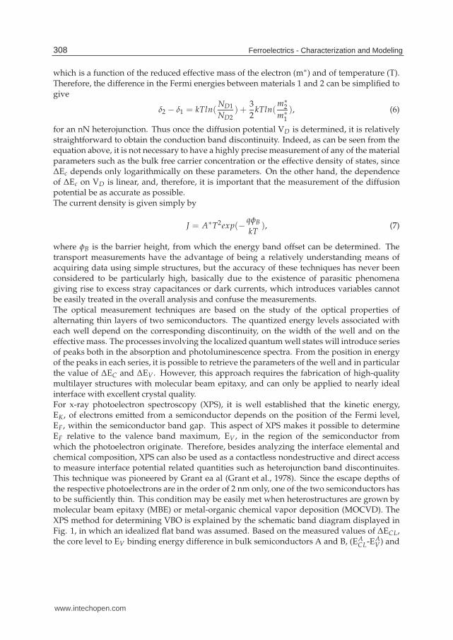
where φB is the barrier height, from which the energy band offset can be determined. Thetransport measurements have the advantage of being a relatively understanding means ofacquiring data using simple structures, but the accuracy of these techniques has never beenconsidered to be particularly high, basically due to the existence of parasitic phenomenagiving rise to excess stray capacitances or dark currents, which introduces variables cannotbe easily treated in the overall analysis and confuse the measurements.The optical measurement techniques are based on the study of the optical properties ofalternating thin layers of two semiconductors. The quantized energy levels associated witheach well depend on the corresponding discontinuity, on the width of the well and on theeffective mass. The processes involving the localized quantum well states will introduce seriesof peaks both in the absorption and photoluminescence spectra. From the position in energyof the peaks in each series, it is possible to retrieve the parameters of the well and in particularthe value of ΔEC and ΔEV . However, this approach requires the fabrication of high-qualitymultilayer structures with molecular beam epitaxy, and can only be applied to nearly idealinterface with excellent crystal quality.For x-ray photoelectron spectroscopy (XPS), it is well established that the kinetic energy,EK, of electrons emitted from a semiconductor depends on the position of the Fermi level,EF , within the semiconductor band gap. This aspect of XPS makes it possible to determineEF relative to the valence band maximum, EV , in the region of the semiconductor fromwhich the photoelectron originate. Therefore, besides analyzing the interface elemental andchemical composition, XPS can also be used as a contactless nondestructive and direct accessto measure interface potential related quantities such as heterojunction band discontinuites.This technique was pioneered by Grant ea al (Grant et al., 1978). Since the escape depths ofthe respective photoelectrons are in the order of 2 nm only, one of the two semiconductors hasto be sufficiently thin. This condition may be easily met when heterostructures are grown bymolecular beam epitaxy (MBE) or metal-organic chemical vapor deposition (MOCVD). TheXPS method for determining VBO is explained by the schematic band diagram displayed inFig. 1, in which an idealized flat band was assumed. Based on the measured values of ΔECL,the core level to EV binding energy difference in bulk semiconductors A and B, (EA
CL-EAV ) and
308 Ferroelectrics - Characterization and Modeling
www.intechopen.com
Valence Band Offsets of ZnO/SrTiO3, ZnO/BaTiO3 , InN/SrTiO3 , and InN/BaTiO3 Heterojunctions Measured by X-ray Photoelectron Spectroscopy 5
(EBCL-EB
V), respectively. By inspection of Fig. 1, it can be seen that
ΔEV(B − A) = (EBCL − EB
V)− (EACL − EA
V ) + ΔECL(A − B). (8)
Thus, to apply XPS for ΔEV measurements, it is essential to determine the bulk semiconductormaterial parameters (ECL-EV) for those semiconductors forming the heterojunctions. Aprimary difficulty with measuring (ECL-EV) is the accurate determination of the EV positionin photoemission spectra. The most frequently employed method involves extrapolation of atangent line to the leading edge of the valence band spectrum to the energy axis, this interceptis defined as EV . Substituting these values to Eq. 8, the VBO of heterojunction A/B can beobtained.
incr
easi
ng E
B
BA
ECLB
EcA
EvA
ECLA
EcB
EvB
EgBEg
A
(ECL-Ev)A
(ECL-Ev)B
Ec
Ev
ECL
EB=0EF
Fig. 1. Schematic energy band diagram illustrating the measurement of VBO by XPS.
3. Experimental
Several samples, bulk commercial (001) STO, (111) STO and (001) BTO substrates, thick(several hundred nanometers) and thin (about 5 nm) ZnO and InN layers grown on thecommercial STO and BTO substrates were studied in this work. To get a clean interface,the STO and BTO substrates were cleaned with organic solvents and rinsed with de-ionizedwater sequentially before loading into the reactor. The thick and thin heterostructures ofZnO/STO, ZnO/BTO, InN/STO and InN/BTO were deposited by MOCVD. More growthcondition details of the ZnO and InN layers can be found in our previous reports (Jia et al.,2008; 2009a;b; 2010a;b; 2011; Li et al., 2011).XPSs were performed on ThermoFisher ESCALAB 250, PHI Quantera SXM, and VG MKIIXPS instruments with AlKα (hν=1486.6 eV) as the x-ray radiation source, which had beencarefully calibrated on work function and Fermi energy level (EF). Because all the sampleswere exposed to air, there must be some impurities (e.g., oxygen and carbon) existing in thesample surface, which may prevent the precise determination of the positions of the valenceband maximum (VBM). To reduce the undesirable effects of surface contamination, all thesamples were cleaned by Ar+ bombardment at a low sputtering rate to avoid damage to thesamples. After the bombardment, peaks related to impurities were greatly reduced, and nonew peaks appeared. Because a large amount of electrons are excited and emitted from thesample, the sample is always positively charged and the electric field caused by the charge canaffect the measured kinetic energy of photoelectron. Charge neutralization was performed
309Valence Band Offsets of ZnO/SrTiO3, ZnO/BaTiO3,InN/SrTiO3, and InN/BaTiO3 Heterojunctions Measured by X-Ray Photoelectron Spectroscopy
www.intechopen.com
6 Will-be-set-by-IN-TECH
with an electron flood gun and all XPS spectra were calibrated by the C 1s peak at 284.8 eVfrom contamination to compensate the charge effect. Since only the relative energy position ineach sample is needed to determine the VBO, the absolute energy calibration for a samplehas no effect on the ultimate result. The surfaces of samples were examined initially bylow-resolution survey scans to determine which elements were present. Very high-resolutionspectra were acquired to determine the binding energy of core level (CL) and the valenceband maximum energy in the survey spectra. All the CL spectra were fitted to Voigt (mixedLorentz-Gaussian) line shape with a Shirley background. Since considerable accordance of thefitted line to the original measured data has been obtained, the uncertainty of the CL positionshould be less than 0.03 eV, as evaluated by numerous fittings with different parameters. TheVBM positions in the valence band (VB) spectra were determined by linear extrapolation ofthe leading edge of the VB spectra recorded on bulk substrates and thick films to the baselines in order to account for instrument resolution induced tail (Zhang et al., 2007), whichhas already been widely used to determine the VBM of semiconductors. Evidently, the VBMvalue is sensitive to the choice of points on the leading edge used to obtain the regressionline (Chambers et al., 2001). Thus, several different sets of points were selected over the linearregion of the leading edge to perform regressions, and the uncertainty of VBO is found to beless than 0.06 eV in the present work.
4. VBO for ZnO/STO heterojunction
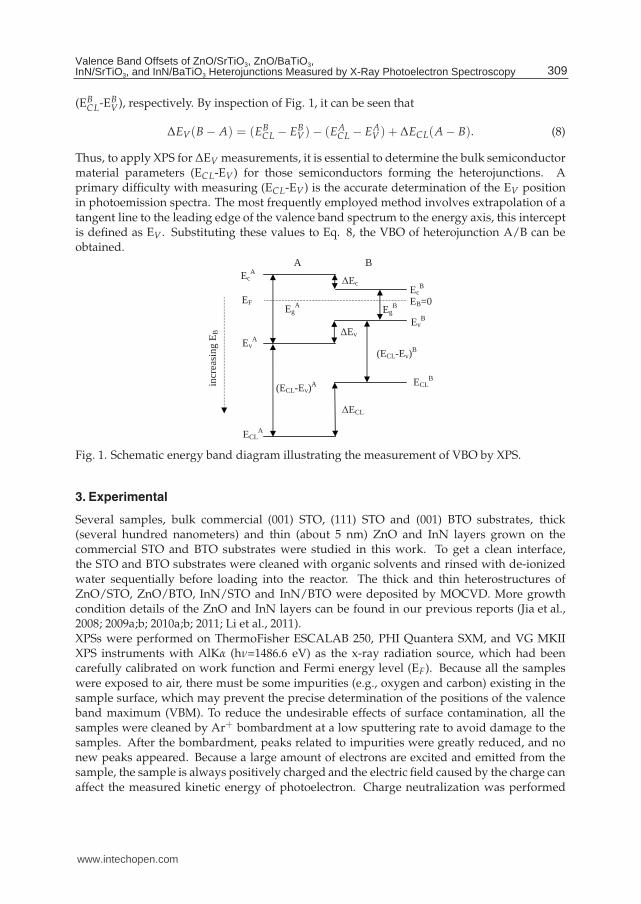
Figure 2 (a) shows the x-ray θ-2θ diffraction patterns of thick ZnO films on (111) STOsubstrates. The diffractogram indicates only a single phase ZnO with a hexagonal wurtzitestructure. Only peaks of ZnO (0002) and (0004) reflection and no other ZnO related peaks areobserved, implying a complete c-axis oriented growth of the ZnO layer. The highly orientedZnO films on STO substrate strongly suggest that the nucleation and crystal growth is initiatednear the substrate surface. The full width at half maximum (FWHM) of symmetric (0002) scanis about 0.85◦ along ω-axis, as shown in the inset of Fig. 2(a). X-ray off-axis φ scans areperformed to identify the in-plane orientation relationships between the film and substrate.The number of peaks in a φ scan corresponds to the number of planes for a particular familythat possesses the same angle with the film surface. Figure 2 (b) shows the results of x-rayφ scans performed using the {1122} reflection of ZnO (2θ=67.95◦ , χ=58.03◦) and the {110}reflection of STO (2θ=32.4◦ , χ=35.26◦). Only six peaks separated by 60◦ are observed for theZnO {112} family, which has six crystal planes with the same angle with the growth plane(χ=58.03◦), as shown in Fig. 2 (b), indicating a single domain. From the relative positionof ZnO {112} and STO {110} families, the in-plane relationships can be determined to be[1120]ZnO‖[011]STO. The atomic arrangement in the (0001) basal plane of ZnO is shownin Fig. 2 (c). The growth in this direction shows a large lattice mismatch of about 17.7%
( 2aZnO−√
2aSTO√2aSTO
×100%) along the direction of <1120>ZnO, although it shows a much smaller
lattice mismatch of 1.91% (√
3aZnO−√
2aSTO√2aSTO
×100%) along the direction of <1100>ZnO when
ZnO rotated 30◦ in plane.For ZnO/STO heterojunction, the VBO (ΔEV) can be calculated from the formula
ΔEV = ΔECL + (EZnOZn2p − EZnO
VBM)− (ESTOTi2p − ESTO
VBM), (9)
310 Ferroelectrics - Characterization and Modeling
www.intechopen.com
Valence Band Offsets of ZnO/SrTiO3, ZnO/BaTiO3 , InN/SrTiO3 , and InN/BaTiO3 Heterojunctions Measured by X-ray Photoelectron Spectroscopy 7
20 30 40 50 60 70 80
-3 -2 -1 0 1 2 3
Inte
nsity
(ar
b. u
nits
.)
(deg.)ST
O(1
11)
ZnO
(004
)ZnO
(002
)
Inte
nsity
(ar
b. u
nits
.)
2 (deg.)0 50 100 150 200 250 300 350
STO{110} (2 =32.40o =35.26o)
ZnO{112} (2 =67.95o =58.03o)
Inte
nsity
(ar
b. u
nits
.)
(deg.)
2 aSTO
aZnO
[1100][211]
[011]
(111)STO
[1120]
(0001)ZnO
(c)
(a) (b)
Fig. 2. X-ray θ-2θ (a), ω (inset of (a)), and φ (b) scans and atomic arrangement (c) of ZnO filmson (111) STO substrate.
where ΔECL=(EZnO/STOTi2p -EZnO/STO
Zn2p ) is the energy difference between Zn 2p and Ti 2p CLs
measured in the thin ZnO/STO heterojunction sample, and (ESTOTi2p-ESTO
VBM) and (EZnOZn2p-EZnO
VBM)
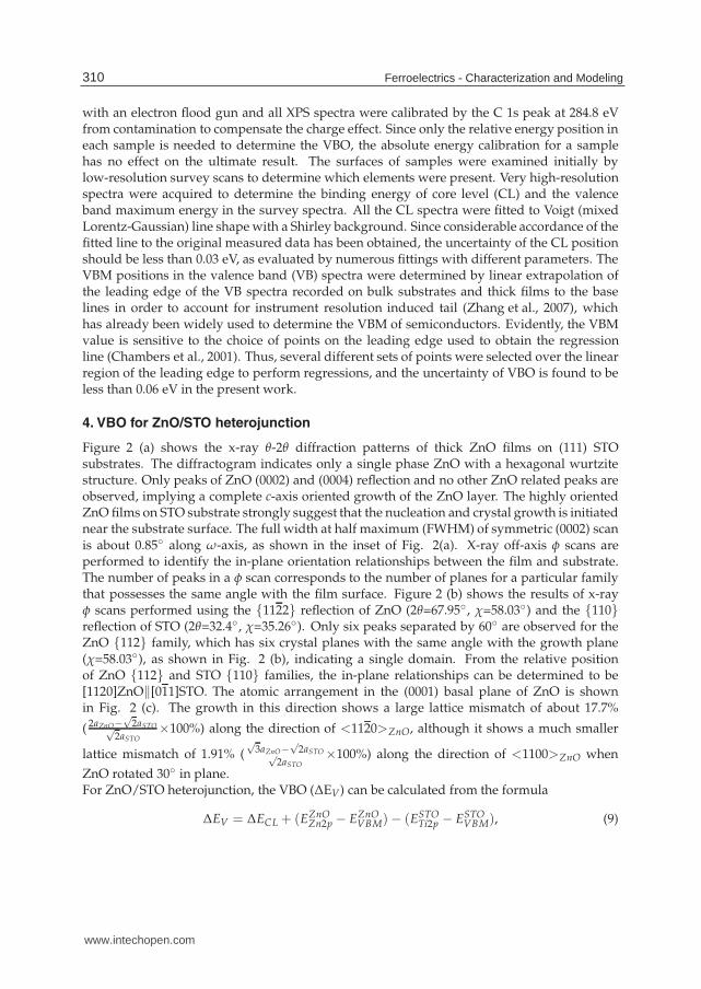
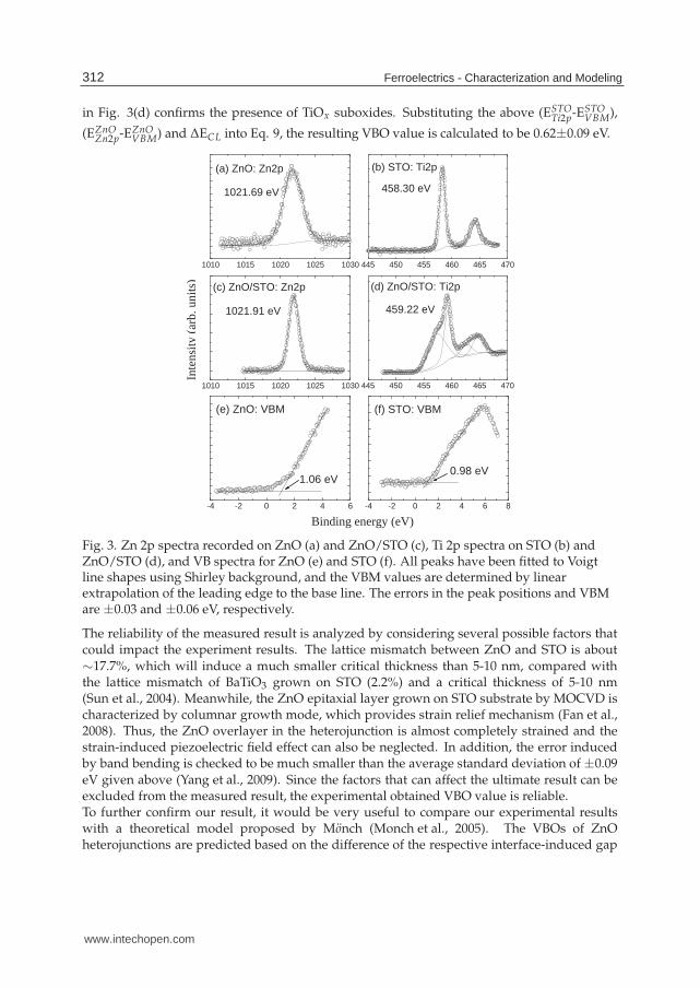
are the VBM energies with reference to the CL positions of bulk STO and thick ZnO film,respectively, which are obtained by XPS measurement from the respective STO substrate andthick ZnO film.Figure 3 shows the XPS Ti 2p and Zn 2p CL narrow scans and the valence band spectrafrom the STO substrate and the thick ZnO/STO samples, respectively. As shown in Fig.3(a), the Zn 2p CL peak locates at 1021.69±0.03 eV. Fig. 3(e) shows the VB spectra of thethick ZnO sample, and the VBM position is determined to be 1.06±0.06 eV by a linear fittingdepicted above. As a result, the energy difference of Zn 2p to ZnO VBM (EZnO
Zn2p-EZnOVBM) can
be determined to be 1020.63±0.03 eV. Using the same Voigt fitting and linear extrapolationmethods mentioned above, the energy difference of Ti2p to STO VBM (ESTO
Ti2p-ESTOVBM) can be
determined to be 457.32±0.06 eV. The CL spectrum of Zn 2p and Ti 2p in thick ZnO filmand bulk STO are quite symmetric indicating the uniform bonding state and the only peakscorrespond to Zn-O and Ti-O bonds, respectively. The measurement of ΔECL for the Ti 2p andZn 2p CLs recorded in the thin ZnO/STO junction is illustrated in Fig. 3(c) and (d). Aftersubstraction of the background, the spectra of Ti 2p and Zn 2p CLs were well Voigt fitted andthe energy difference of Ti 2p and Zn 2p CLs (ΔECL) can be determined to be 562.69±0.03eV. It is noteworthy that the Ti 2p peak is not symmetric and consists of two components bycareful Voigt fitting. The prominent one located at 459.22 eV is attributed to the Ti emitterswithin the STO substrate which have six bonds to oxygen atoms, and the other one shiftingby ∼2 eV to a lower binding energy indicates the presence of an interfacial oxide layer. Thisphenomenon is similar to that observed in the interface of LaAlO3/SrTiO3, and the shoulderat lower binding energy is attributed to TiOx suboxides, which is expected on account of theTiOx-terminated STO initial surface (Kazzi et al., 2006). The fair double-peak fitting shown
311Valence Band Offsets of ZnO/SrTiO3, ZnO/BaTiO3,InN/SrTiO3, and InN/BaTiO3 Heterojunctions Measured by X-Ray Photoelectron Spectroscopy
www.intechopen.com
8 Will-be-set-by-IN-TECH
in Fig. 3(d) confirms the presence of TiOx suboxides. Substituting the above (ESTOTi2p-ESTO
VBM),
(EZnOZn2p-EZnO
VBM) and ΔECL into Eq. 9, the resulting VBO value is calculated to be 0.62±0.09 eV.
1010 1015 1020 1025 1030
(a) ZnO: Zn2p
1021.69 eV
-4 -2 0 2 4 6
1.06 eV
(e) ZnO: VBM
-4 -2 0 2 4 6 8
0.98 eV
(f) STO: VBM
445 450 455 460 465 470
(b) STO: Ti2p
458.30 eV
1010 1015 1020 1025 1030
(c) ZnO/STO: Zn2p
1021.91 eV
445 450 455 460 465 470
(d) ZnO/STO: Ti2p
459.22 eV
Binding energy (eV)
Inte
nsit
y(a
rb. u
nits
)
Fig. 3. Zn 2p spectra recorded on ZnO (a) and ZnO/STO (c), Ti 2p spectra on STO (b) andZnO/STO (d), and VB spectra for ZnO (e) and STO (f). All peaks have been fitted to Voigtline shapes using Shirley background, and the VBM values are determined by linearextrapolation of the leading edge to the base line. The errors in the peak positions and VBMare ±0.03 and ±0.06 eV, respectively.
The reliability of the measured result is analyzed by considering several possible factors thatcould impact the experiment results. The lattice mismatch between ZnO and STO is about∼17.7%, which will induce a much smaller critical thickness than 5-10 nm, compared withthe lattice mismatch of BaTiO3 grown on STO (2.2%) and a critical thickness of 5-10 nm(Sun et al., 2004). Meanwhile, the ZnO epitaxial layer grown on STO substrate by MOCVD ischaracterized by columnar growth mode, which provides strain relief mechanism (Fan et al.,2008). Thus, the ZnO overlayer in the heterojunction is almost completely strained and thestrain-induced piezoelectric field effect can also be neglected. In addition, the error inducedby band bending is checked to be much smaller than the average standard deviation of ±0.09eV given above (Yang et al., 2009). Since the factors that can affect the ultimate result can beexcluded from the measured result, the experimental obtained VBO value is reliable.To further confirm our result, it would be very useful to compare our experimental resultswith a theoretical model proposed by Monch (Monch et al., 2005). The VBOs of ZnOheterojunctions are predicted based on the difference of the respective interface-induced gap
312 Ferroelectrics - Characterization and Modeling
www.intechopen.com
Valence Band Offsets of ZnO/SrTiO3, ZnO/BaTiO3 , InN/SrTiO3 , and InN/BaTiO3 Heterojunctions Measured by X-ray Photoelectron Spectroscopy 9
states (IFIGS) branch-point energies and electric dipole terms. That is
ΔEV = Evl(Γ)− Evr(Γ) = φpbpr − φ
pbpl + DX(Xsr − Xsl), (10)
where the p-type branch-point energy φpbp(Γ) = Ebp − EV(Γ) is the energy distance from the
valence band maximum to the branch point of the IFIGS and Xs is the electronegativity of therespective semiconductor. The subscripts r and l stand for the right and left side, respectively,of the heterostructure. The dipole parameter DX is determined by the density of states andextension of the IFIGS at their branch point. This dipole term can also be neglected, justlike the common semiconductor heterojunctions, since the electronegativities of the atomsconstituting ZnO/STO heterojunction differ by up to 10% only. Through analysis of the VBOvalues reported for ZnO heterostructure (Monch et al., 2005), the dependence of VBO on thep-type branch-point energy is obtained to be
ΔEV = ϕvbo[φpbp(ZnO)− φ
pbp(semi)]. (11)
With the p-type branch-point energies of ZnO (3.04 eV) (Monch et al., 2005) and STO (2.5eV) (Monch et al., 2004), and the slope parameters ϕvbo for insulator heterostructures of1.14∼1.23, a VBO of 0.64±0.21 eV would be calculated, which is in good agreement withthe experimentally determined value of 0.62±0.09 eV. It implies that the IFIGS theory is notonly widely used to the group-IV elemental semiconductors, SiC, and the III-V, II-VI, andI-III-VI2 compound semiconductors and their alloys (Monch et al., 2005), but also applicable tothe semiconductor/insulator heterostructures. In addition, the resulting ΔEV is a sufficientlylarge value for device applications in which strong carrier confinement is needed, such aslight emitters or heterostructure field effect transistors. For instance, the valence band offsetin the Zn0.95Cd0.05O/ZnO system is only 0.17 eV (Chen et al., 2005), which is less than that ofZnO/STO.Finally, the CBO (ΔEC) can be estimated by the formula ΔEC=ΔEV+EZnO
g -ESTOg . By
substituting the band gap values (EZnOg =3.37 eV (Su et al., 2008) and ESTO
g =3.2 eV (Baer et al.,1967)), ΔEC is calculated to be 0.79±0.09 eV. It would be interesting to compareour experimental values with the electrical transport results by Wu et al (Wu et al.,2008). They have investigated the temperature dependent current-voltage characteristic ofZnO/Nb:SrTiO3 junction, and found that the effective barrier height (φe f f ) is 0.73 eV, whichis directly considered to be the CBO in n-N heterojunctions (Alivov et al., 2006). It can be seenthat the effective barrier height in Wu’s work is consistent with our CBO value. Accordingly,a type-II band alignment forms at the heterojunction interface, in which the conduction andvalence bands of the ZnO film are concomitantly higher than those of the STO substrate, asshown in Fig. 4.
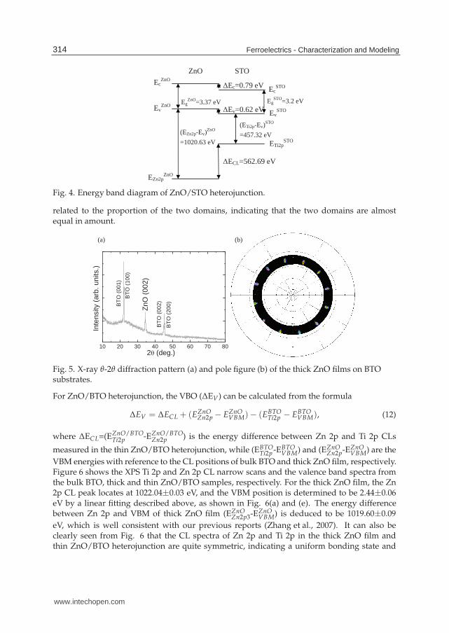
5. VBO for ZnO/BTO heterojunction
In x-ray θ-2θ diffraction measurements, as shown in Fig. 5 (a), the ZnO/BTO sample presentedthe only peak of ZnO (0002) reflection and no other ZnO related peaks were observed,implying a complete c-axis oriented growth of the ZnO layer. From the pole figure of ZnO{1011} family, shown in Fig. 5 (b), twelve peaks separated by 30◦ are present, although ZnOhas a sixfold symmetry about the [0001] axis, indicating that the ZnO film is twinned in thegrowth plane by a 30◦ in-plane rotation. The relative intensities of the two sets of peaks is
313Valence Band Offsets of ZnO/SrTiO3, ZnO/BaTiO3,InN/SrTiO3, and InN/BaTiO3 Heterojunctions Measured by X-Ray Photoelectron Spectroscopy
www.intechopen.com
10 Will-be-set-by-IN-TECH
STO ZnO
ETi2pSTO
EcZnO
EvZnO
EZn2pZnO
EcSTO
EvSTO
EgSTO=3.2 eV Eg
ZnO=3.37 eV
(EZn2p-Ev)ZnO
=1020.63 eV
(ETi2p-Ev)STO
=457.32 eV
Ec=0.79 eV
Ev=0.62 eV
ECL=562.69 eV
Fig. 4. Energy band diagram of ZnO/STO heterojunction.
related to the proportion of the two domains, indicating that the two domains are almostequal in amount.
10 20 30 40 50 60 70 80
BT
O (
200)
BT
O (
002)
BT
O (
100)
BT
O (
001)
ZnO
(00
2)
Inte
nsity
(ar
b. u
nits
.)
2 (deg.)
(a) (b)
Fig. 5. X-ray θ-2θ diffraction pattern (a) and pole figure (b) of the thick ZnO films on BTOsubstrates.
For ZnO/BTO heterojunction, the VBO (ΔEV) can be calculated from the formula
ΔEV = ΔECL + (EZnOZn2p − EZnO
VBM)− (EBTOTi2p − EBTO
VBM), (12)
where ΔECL=(EZnO/BTOTi2p -EZnO/BTO
Zn2p ) is the energy difference between Zn 2p and Ti 2p CLs
measured in the thin ZnO/BTO heterojunction, while (EBTOTi2p -EBTO
VBM) and (EZnOZn2p-EZnO
VBM) are the
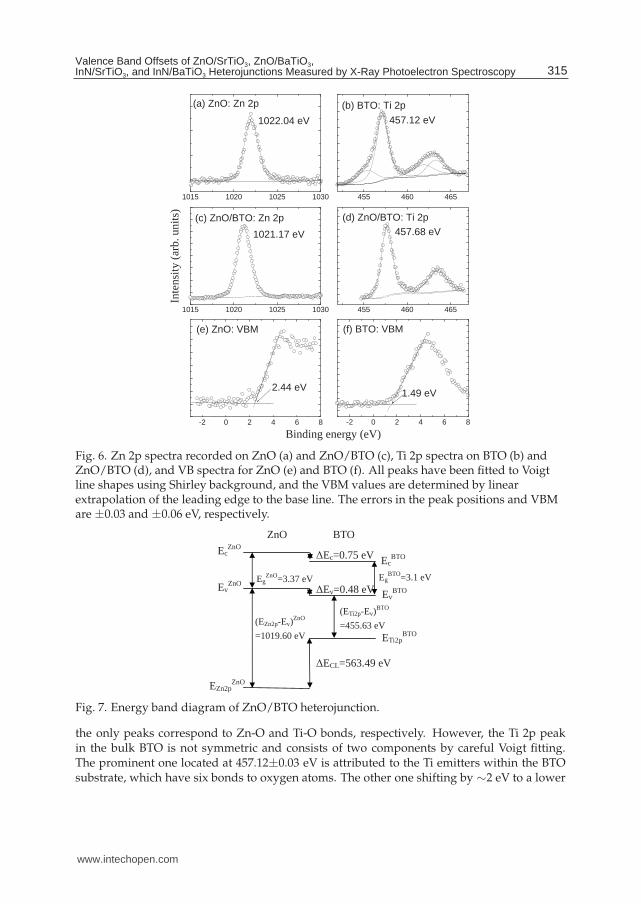
VBM energies with reference to the CL positions of bulk BTO and thick ZnO film, respectively.Figure 6 shows the XPS Ti 2p and Zn 2p CL narrow scans and the valence band spectra fromthe bulk BTO, thick and thin ZnO/BTO samples, respectively. For the thick ZnO film, the Zn2p CL peak locates at 1022.04±0.03 eV, and the VBM position is determined to be 2.44±0.06eV by a linear fitting described above, as shown in Fig. 6(a) and (e). The energy differencebetween Zn 2p and VBM of thick ZnO film (EZnO
Zn2p3-EZnOVBM) is deduced to be 1019.60±0.09
eV, which is well consistent with our previous reports (Zhang et al., 2007). It can also beclearly seen from Fig. 6 that the CL spectra of Zn 2p and Ti 2p in the thick ZnO film andthin ZnO/BTO heterojunction are quite symmetric, indicating a uniform bonding state and
314 Ferroelectrics - Characterization and Modeling
www.intechopen.com
Valence Band Offsets of ZnO/SrTiO3, ZnO/BaTiO3 , InN/SrTiO3 , and InN/BaTiO3 Heterojunctions Measured by X-ray Photoelectron Spectroscopy 11
-2 0 2 4 6 8
2.44 eV
(e) ZnO: VBM
-2 0 2 4 6 8
1.49 eV
(f) BTO: VBM
455 460 465
457.12 eV
(b) BTO: Ti 2p
1015 1020 1025 1030
(a) ZnO: Zn 2p
1022.04 eV
1015 1020 1025 1030
(c) ZnO/BTO: Zn 2p
1021.17 eV
455 460 465
457.68 eV(d) ZnO/BTO: Ti 2p
Binding energy (eV)
Inte
nsity
(ar
b. u
nits
)
Fig. 6. Zn 2p spectra recorded on ZnO (a) and ZnO/BTO (c), Ti 2p spectra on BTO (b) andZnO/BTO (d), and VB spectra for ZnO (e) and BTO (f). All peaks have been fitted to Voigtline shapes using Shirley background, and the VBM values are determined by linearextrapolation of the leading edge to the base line. The errors in the peak positions and VBMare ±0.03 and ±0.06 eV, respectively.
BTO ZnO
ETi2pBTO
EcZnO
EvZnO
EZn2pZnO
EcBTO
EvBTO
EgBTO=3.1 eV Eg
ZnO=3.37 eV
(EZn2p-Ev)ZnO
=1019.60 eV
(ETi2p-Ev)BTO
=455.63 eV
Ec=0.75 eV
Ev=0.48 eV
ECL=563.49 eV
Fig. 7. Energy band diagram of ZnO/BTO heterojunction.
the only peaks correspond to Zn-O and Ti-O bonds, respectively. However, the Ti 2p peakin the bulk BTO is not symmetric and consists of two components by careful Voigt fitting.The prominent one located at 457.12±0.03 eV is attributed to the Ti emitters within the BTOsubstrate, which have six bonds to oxygen atoms. The other one shifting by ∼2 eV to a lower
315Valence Band Offsets of ZnO/SrTiO3, ZnO/BaTiO3,InN/SrTiO3, and InN/BaTiO3 Heterojunctions Measured by X-Ray Photoelectron Spectroscopy
www.intechopen.com
12 Will-be-set-by-IN-TECH
binding energy is attributed to TiOx suboxides on account of the TiO-terminated BTO initialsurface (Kazzi et al., 2006). It is interesting that the Ti 2p peaks transform from asymmetryin bulk BTO to symmetry in the thin ZnO/BTO sample, implying that the TiOx suboxidesin the BTO surface is oxidized completely to the highest valence of Ti4+. The VBM value ofbulk BTO is determined to be 1.49±0.06 eV using the linear method. The Fermi level of aninsulator is expected to be located in the middle of the forbidden energy gap, so the VBMwill be one-half of the band gap of insulators (You et al., 2009). For BTO, the VBM shouldbe 1.55 eV calculated from the band gap of 3.1 eV (Boggess et al., 1990), which is in goodagreement with the measured value (1.49±0.06 eV) in the present work. Using the same fittingmethods mentioned above, the energy values of CL for the thin ZnO/BTO heterojunction canbe determined, as shown in Fig. 6. Substituting the above values into Eq. 12, the resultingVBO value is calculated to be 0.48±0.09 eV.A small lattice mismatch is present between the BTO[011] direction and the hexagonal
apothem of ZnO, which is only about 0.8% (√
3aZnO−√
2aBTO√2aBTO
×100%) (Wei et al., 2007). This
lattice mismatch is so small that the strain-induced piezoelectric field effect can be neglectedin this work (Su et al., 2008). In ZnO/MgO heterostructure, the 8.3% mismatch brings a shiftof 0.22 eV on VBO (Li et al., 2008). By linear extrapolation method, the strain induced shift inZnO/BTO is less than 0.02 eV, which is much smaller than the aforementioned deviation of0.09 eV. The error induced by band bending is checked to be much smaller than the averagestandard deviation of 0.09 eV given above (Yang et al., 2009). So the experimental obtainedVBO value is reliable.To further confirm the reliability of the experimental values, it would be useful to compareour VBO value with other results deduced by transitive property. For heterojunctions formedbetween all pairs of three materials (A, B, and C), ΔEV(A-C) can be deduced from thedifference between ΔEV(A-B) and ΔEV(C-B) neglecting the interface effects (Foulon et al.,1992). The reported VBO values for some heterojunctions are ΔEV(ZnO-STO)=0.62 eV(Jia et al., 2009b), ΔEV(Si-STO)=2.38 or 2.64 eV, and ΔEV(Si-BTO)=2.35 or 2.66 eV (Amy et al.,2004), respectively. Then the ΔEV(ZnO-BTO) is deduced to be 0.59, 0.64, 0.9 or 0.33 eV, whichis comparable to our measured value 0.48±0.09 eV. Since the samples were prepared underdifferent growth conditions, the different interfaces are responsible for the difference betweenour measured value and the results from the transitivity. In addition, the resulting ΔEV is asufficiently large value for device applications which require strong carrier confinement, suchas light emitters or heterostructure field effect transistors (Chen et al., 2005).Finally, the CBO (ΔEC) can be estimated by the formula ΔEC=ΔEV+EZnO
g -EBTOg . By
substituting the band gap values at room temperature (EZnOg =3.37 eV (Su et al., 2008) and
EBTOg =3.1 eV (Boggess et al., 1990)), ΔEC is calculated to be 0.75±0.09 eV. Accordingly, a type-II
band alignment forms at the heterojunction interface, in which the conduction and valencebands of the ZnO film are concomitantly higher than those of the BTO substrate, as shown inFig. 7.
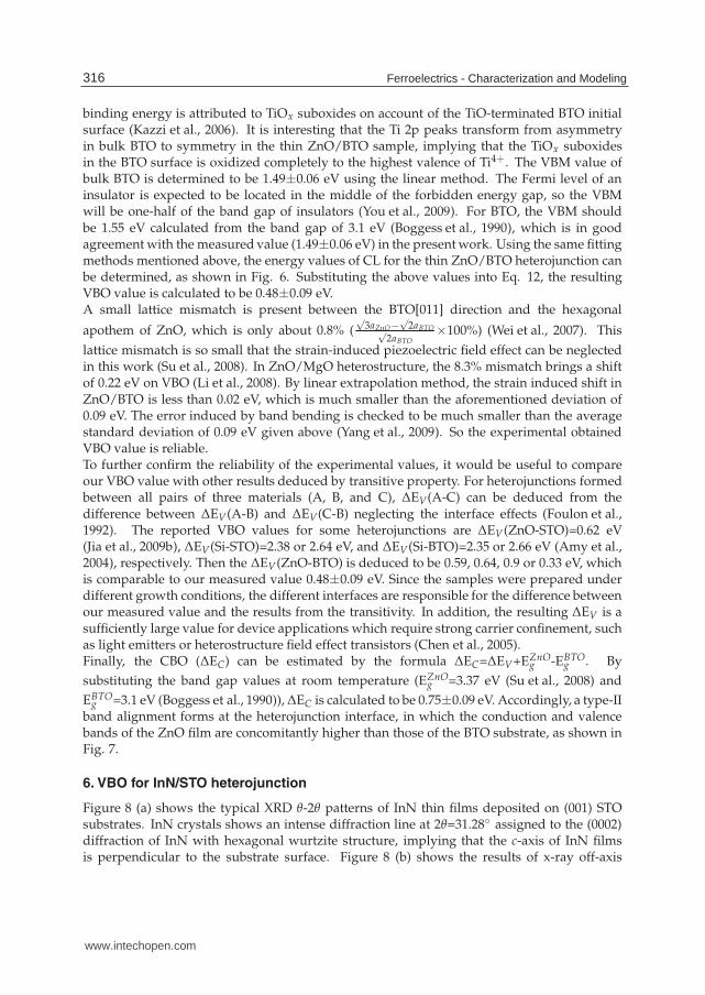
6. VBO for InN/STO heterojunction
Figure 8 (a) shows the typical XRD θ-2θ patterns of InN thin films deposited on (001) STOsubstrates. InN crystals shows an intense diffraction line at 2θ=31.28◦ assigned to the (0002)diffraction of InN with hexagonal wurtzite structure, implying that the c-axis of InN filmsis perpendicular to the substrate surface. Figure 8 (b) shows the results of x-ray off-axis
316 Ferroelectrics - Characterization and Modeling
www.intechopen.com
Valence Band Offsets of ZnO/SrTiO3, ZnO/BaTiO3 , InN/SrTiO3 , and InN/BaTiO3 Heterojunctions Measured by X-ray Photoelectron Spectroscopy 13
φ scans performed using the {1011} reflection of InN (2θ=33.49◦ , χ=61.86◦) and the {111}reflection of STO (2θ=39.96◦ , χ=54.74◦) to determine the in-plane orientation of the InN filmrelative to STO. Although InN has a sixfold symmetry about the [0001] axis, the presence oftwelve peaks separated by 30◦ for {1122} reflections indicates that the InN films is twinnedin the growth plane by a 30◦ in-plane rotation. The relative intensities of the two sets ofpeaks is related to the proportion of the two domains, indicating almost the same amountfor the two domains. Comparing the locations in φ-space of the InN{1011} with STO{111}families, the two-dimensional epitaxial relationships for the two domains can be derived tobe [1100]InN‖[110]STO for one domain and [1120]InN‖[110]STO for the other. The atomicarrangements for the two domains are illustrated in the schematic drawings of Fig. 8(c).
20 30 40 50 60 70 80
InN
(112
)In
N(0
04)
ST
O(0
03)
ST
O(0
02)
Inte
nsity
(ar
b. u
nits
.)
2 (deg.)
InN
(002
)
ST
O(0
01)
K
-150 -100 -50 0 50 100 150
STO{111} (2 =39.96o, =54.74o)
InN{101} (2 =33.49o, =61.86o)
(deg.)
(b)(a)
aSTO
aInN aInN
(c)
Fig. 8. X-ray θ-2θ (a) and φ (b) scanning patterns, and atomic arrangement (c) of the thick InNfilms on (001)STO substrates.
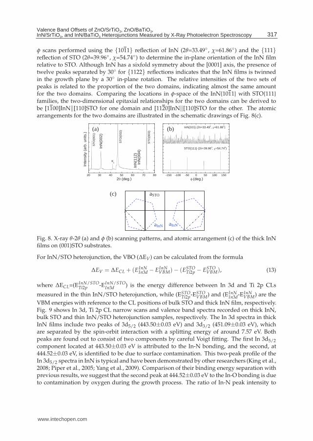
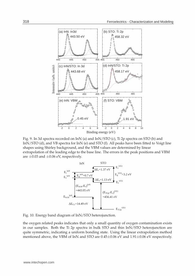
For InN/STO heterojunction, the VBO (ΔEV) can be calculated from the formula
ΔEV = ΔECL + (EInNIn3d − EInN
VBM)− (ESTOTi2p − ESTO
VBM), (13)
where ΔECL=(EInN/STOTi2p -EInN/STO
In3d ) is the energy difference between In 3d and Ti 2p CLs
measured in the thin InN/STO heterojunction, while (ESTOTi2p-ESTO
VBM) and (EInNIn3d-EInN
VBM) are the
VBM energies with reference to the CL positions of bulk STO and thick InN film, respectively.Fig. 9 shows In 3d, Ti 2p CL narrow scans and valence band spectra recorded on thick InN,bulk STO and thin InN/STO heterojunction samples, respectively. The In 3d spectra in thickInN films include two peaks of 3d5/2 (443.50±0.03 eV) and 3d3/2 (451.09±0.03 eV), whichare separated by the spin-orbit interaction with a splitting energy of around 7.57 eV. Bothpeaks are found out to consist of two components by careful Voigt fitting. The first In 3d5/2
component located at 443.50±0.03 eV is attributed to the In-N bonding, and the second, at444.52±0.03 eV, is identified to be due to surface contamination. This two-peak profile of theIn 3d5/2 spectra in InN is typical and have been demonstrated by other researchers (King et al.,2008; Piper et al., 2005; Yang et al., 2009). Comparison of their binding energy separation withprevious results, we suggest that the second peak at 444.52±0.03 eV to the In-O bonding is dueto contamination by oxygen during the growth process. The ratio of In-N peak intensity to
317Valence Band Offsets of ZnO/SrTiO3, ZnO/BaTiO3,InN/SrTiO3, and InN/BaTiO3 Heterojunctions Measured by X-Ray Photoelectron Spectroscopy
www.intechopen.com
14 Will-be-set-by-IN-TECH
-2 0 2 4 6 8
0.45 eV
(e) InN: VBM
-2 0 2 4 6 8 10
(f) STO: VBM
1.91 eV
440 445 450 455
(a) InN: In3d
443.50 eV
455 460 465
(b) STO: Ti 2p
458.32 eV
440 445 450 455
(c) InN/STO: In 3d
443.68 eV
455 460 465
(d) InN/STO: Ti 2p
458.17 eV
Binding energy (eV)
Inte
nsit
y(a
rb. u
nits
)
Fig. 9. In 3d spectra recorded on InN (a) and InN/STO (c), Ti 2p spectra on STO (b) andInN/STO (d), and VB spectra for InN (e) and STO (f). All peaks have been fitted to Voigt lineshapes using Shirley background, and the VBM values are determined by linearextrapolation of the leading edge to the base line. The errors in the peak positions and VBMare ±0.03 and ±0.06 eV, respectively.
STO InN
ETi2pSTO
EcInN
EvInN
EIn3dInN
EcSTO
EvSTO
EgSTO=3.2 eV Eg
InN=0.7 eV
(EIn3d-Ev)InN
=443.05 eV (ETi2p-Ev)
STO
=456.41 eV
Ec=1.37 eV
Ev=1.13 eV
ECL=14.49 eV
Fig. 10. Energy band diagram of InN/STO heterojunction.
the oxygen related peaks indicates that only a small quantity of oxygen contamination existsin our samples. Both the Ti 2p spectra in bulk STO and thin InN/STO heterojunction arequite symmetric, indicating a uniform bonding state. Using the linear extrapolation methodmentioned above, the VBM of InN and STO are 0.45±0.06 eV and 1.91±0.06 eV respectively.
318 Ferroelectrics - Characterization and Modeling
www.intechopen.com
Valence Band Offsets of ZnO/SrTiO3, ZnO/BaTiO3 , InN/SrTiO3 , and InN/BaTiO3 Heterojunctions Measured by X-ray Photoelectron Spectroscopy 15
Compared with the spectra recorded on the InN and STO samples, the In 3d core level shiftsto 443.68±0.03 eV and Ti 2p shifts to 458.17±0.03 eV in thin InN/STO heterojunction. TheVBO value is calculated to be 1.13±0.09 eV by substituting those values into Eq. 13.Reliability of the analysis of the measured results is provided by considering possible factorsthat could impact the experimental results. InN is a kind of piezoelectric crystal, so the strainexisting in the InN overlayer of the heterojunction will induce piezoelectric field and affect the
results. The lattice mismatch between InN and STO is larger than 9.8% (√
3a InN−√
2aSTO√2aSTO
×100%),
so the InN layer can be approximately treated as completely relaxed and this approximationshould not introduce much error in our result. In addition, the energy band bends downwardat the surface of InN film and there is an electron accumulation layer (Mahboob et al., 2004),so the energy separation between VBM and Fermi level can be changed at the InN surface,which could impact the measured VBO values of the heterojunctions. However, both the CLemissions of In 3d and Ti 2p at the InN/STO heterojunction are collected from the same surface(InN surface), thus, the surface band bending effects can be canceled out for the measurementof ΔECL, as was the measurement of the band offset of the InN/AlN heterojunction by others(King et al., 2007; Wu et al., 2006). Since the factors that can affect the results can be excludedfrom the measured results, the experimental obtained VBO value is reliable.Making use of the band gap of InN (0.7 eV) (Yang et al., 2009) and SrTiO3 (3.2 eV) (Baer et al.,1967), the CBO (ΔEC) is calculated to be 1.37 eV and the ratio of ΔEC/ΔEV is close to 1:1. Asshown in Fig. 10, a type-I heterojunction is seen to be formed in the straddling configuration.So STO can be utilized as the gate oxide for InN based metal-oxide semiconductor, thegate leakage is expected to be negligible, which is different from the Si based devices(Chambers et al., 2000).
7. VBO for InN/BTO heterojunction
10 20 30 40 50 60 70 80
Inte
nsity
(ar
b. u
nits
.)
InN
(00
2)
BT
O (
200)
BT
O (
002)
BT
O (
100)
BT
O (
001)
2 (deg.)
Fig. 11. X-ray θ-2θ scanning patterns of the thick InN films on BTO substrates.
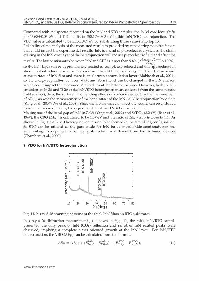
In x-ray θ-2θ diffraction measurements, as shown in Fig. 11, the thick InN/BTO samplepresented the only peak of InN (0002) reflection and no other InN related peaks wereobserved, implying a complete c-axis oriented growth of the InN layer. For InN/BTOheterojunction, the VBO (ΔEV) can be calculated from the formula
ΔEV = ΔECL + (EInNIn3d − EInN
VBM)− (EBTOTi2p − EBTO
VBM), (14)
319Valence Band Offsets of ZnO/SrTiO3, ZnO/BaTiO3,InN/SrTiO3, and InN/BaTiO3 Heterojunctions Measured by X-Ray Photoelectron Spectroscopy
www.intechopen.com
16 Will-be-set-by-IN-TECH
-2 0 2 4 6 8
1.49 eV
(f) BTO: VBM
455 460 465
457.12 eV
(b) BTO: Ti 2p
Binding energy (eV)
Inte
nsity
(ar
b. u
nits
)
455 460 465
458.43 eV
(d) InN/BTO: Ti 2p
-4 -2 0 2 4 6 8
0.24 eV
(e) InN: VBM
440 445 450 455
443.98 eV
(c) InN/BTO: In 3d
440 445 450 455
443.67 eV
(a) InN: In 3d
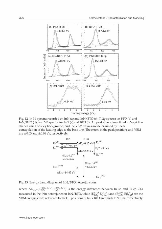
Fig. 12. In 3d spectra recorded on InN (a) and InN/BTO (c), Ti 2p spectra on BTO (b) andInN/BTO (d), and VB spectra for InN (e) and BTO (f). All peaks have been fitted to Voigt lineshapes using Shirley background, and the VBM values are determined by linearextrapolation of the leading edge to the base line. The errors in the peak positions and VBMare ±0.03 and ±0.06 eV, respectively.
BTO InN
ETi2pBTO
EcInN
EvInN
EIn3dInN
EcBTO
EvBTO
EgBTO=3.1 eV
EgInN=0.7 eV
(EIn3d-Ev)InN
=443.43 eV
(ETi2p-Ev)BTO
=455.63 eV
Ec=0.15 eV
Ev=2.25 eV
ECL=14.45 eV
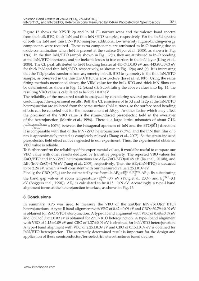
Fig. 13. Energy band diagram of InN/BTO heterojunction.
where ΔECL=(EInN/BTOTi2p -EInN/BTO
In3d ) is the energy difference between In 3d and Ti 2p CLs
measured in the thin heterojunction InN/BTO, while (EBTOTi2p -EBTO
VBM) and (EInNIn3d-EInN
VBM) are the
VBM energies with reference to the CL positions of bulk BTO and thick InN film, respectively.
320 Ferroelectrics - Characterization and Modeling
www.intechopen.com
Valence Band Offsets of ZnO/SrTiO3, ZnO/BaTiO3 , InN/SrTiO3 , and InN/BaTiO3 Heterojunctions Measured by X-ray Photoelectron Spectroscopy 17
Figure 12 shows the XPS Ti 2p and In 3d CL narrow scans and the valence band spectrafrom the bulk BTO, thick InN and thin InN/BTO samples, respectively. For the In 3d spectraof both the InN and thin InN/BTO samples, additional low intensity higher-binding-energycomponents were required. These extra components are attributed to In-O bonding due tooxide contamination when InN is present at the surface (Piper et al., 2005), as shown in Fig.12(a). In the thin InN/BTO sample shown in Fig. 12(c), they are attributed to In-O bondingat the InN/BTO interfaces, and/or inelastic losses to free carriers in the InN layer (King et al.,2008). The CL peak attributed to In-N bonding locates at 443.67±0.03 eV and 443.98±0.03 eVfor thick InN and thin InN/BTO, respectively, as shown in Fig. 12(a) and (c). It is interestingthat the Ti 2p peaks transform from asymmetry in bulk BTO to symmetry in the thin InN/BTOsample, as observed in the thin ZnO/BTO heterostructure (Jia et al., 2010b). Using the samefitting methods mentioned above, the VBM value for the bulk BTO and thick InN films canbe determined, as shown in Fig. 12 (e)and (f). Substituting the above values into Eq. 14, theresulting VBO value is calculated to be 2.25±0.09 eV.The reliability of the measured result is analyzed by considering several possible factors thatcould impact the experiment results. Both the CL emissions of In 3d and Ti 2p at the InN/BTOheterojunction are collected from the same surface (InN surface), so the surface band bendingeffects can be canceled out for the measurement of ΔECL. Another factor which may affectthe precision of the VBO value is the strain-induced piezoelectric field in the overlayerof the heterojunction (Martin et al., 1996). There is a large lattice mismatch of about 7.1%
(√
3a InN−√
2aBTO√2aBTO
×100%) between the hexagonal apothem of InN and the BTO[011] direction.
It is comparable with that of the InN/ZnO heterojunction (7.7%), and the InN thin film of 5nm is approximately treated as completely relaxed (Zhang et al., 2007). So the strain-inducedpiezoelectric field effect can be neglected in our experiment. Thus, the experimental obtainedVBO value is reliable.To further confirm the reliability of the experimental values, it would be useful to compare ourVBO value with other results deduced by transitive property. The reported VBO values forZnO/BTO and InN/ZnO heterojunctions are ΔEV(ZnO-BTO)=0.48 eV (Jia et al., 2010b), andΔEV(InN-ZnO)=1.76 eV (Yang et al., 2009), respectively. Then the ΔEV(InN-BTO) is deducedto be 2.24 eV, which is well consistent with our measured value 2.25±0.09 eV.Finally, the CBO (ΔEC) can be estimated by the formula ΔEC=EBTO
g -EInNg -ΔEV . By substituting
the band gap values at room temperature (EInNg =0.7 eV (Yang et al., 2009) and EBTO
g =3.1eV (Boggess et al., 1990)), ΔEC is calculated to be 0.15±0.09 eV. Accordingly, a type-I bandalignment forms at the heterojunction interface, as shown in Fig. 13.
8. Conclusions
In summary, XPS was used to measure the VBO of the ZnO(or InN)/STO(or BTO)heterojunctions. A type-II band alignment with VBO of 0.62±0.09 eV and CBO of 0.79±0.09 eVis obtained for ZnO/STO heterojunction. A type-II band alignment with VBO of 0.48±0.09 eVand CBO of 0.75±0.09 eV is obtained for ZnO/BTO heterojunction. A type-I band alignmentwith VBO of 1.13±0.09 eV and CBO of 1.37±0.09 eV is obtained for InN/STO heterojunction.A type-I band alignment with VBO of 2.25±0.09 eV and CBO of 0.15±0.09 eV is obtained forInN/BTO heterojuncion. The accurately determined result is important for the design andapplication of these semiconductor/ferroelectric heterostructures based devices.
321Valence Band Offsets of ZnO/SrTiO3, ZnO/BaTiO3,InN/SrTiO3, and InN/BaTiO3 Heterojunctions Measured by X-Ray Photoelectron Spectroscopy
www.intechopen.com

18 Will-be-set-by-IN-TECH
9. Acknowledgements
This work was supported by the 973 program (2006CB604908, 2006CB921607), and theNational Natural Science Foundation of China (60625402, 60990313).
10. References
Alivov Y. I.; Xiao B.; Fan Q.; Morkoc H. & Johnstone D. (2006). Appl. Phys. Lett., Vol. 89, 152115Amy F.; Wan A. S.; Kahn A.; Walker F. J. & Mckee R. A. (2004). J. Appl. Phys., Vol. 96, 1635Baer W. S. (1967). J. Phys. Chem. Solids, Vol. 28, 677Boggess T. F.; White J. O. & Valley G. C. (1990). J. Opt. Soc. Am. B., Vol. 7, 2255Brandt M.; Frenzel H.; Hochmuth H.; Lorentz M.; Grundmann M. & Schubert J. (2009). J. Vac.
Sci. Technol. B, Vol. 27, 1789Capasso F. & Margaritondo G. (1987). Heterojunction band discontinuities: Physics and device
applications, (115-377), Elsevier, 0444870601, North-Holland, Amsterdam OxfordNew York Tokyo
Chambers S. A.; Liang Y.; Yu Z.; Droopad R.; Ramdani J & Eisenbeiser (2000). Appl. Phys. Lett,Vol. 77, 1662
Chambers S. A.; Liang Y.; Yu Z.; Droopad R. & Ramdani J (2001). J. Vac. Sci. Technol. A, Vol. 19,934
Chen J. J.; Ren F.; Li Y. J.; Norton D. P.; Pearton S. J.; Osinsky A.; Dong J. W.; Chow P. P. &Weaver J. F. (2005). Appl. Phys. Lett., Vol. 87, 192106
Cimalla V.; Lebedev V.; Wang C. Y.; Ali M.; Cke G. E.; Polyakov V. M.; Schwierz F.; AmbacherO.; Lu H. & Schaff W. J. (2007). Appl. Phys. Lett., Vol. 90, 152106
Fan H. B.; Sun, G. S.; Yang S. Y.; Zhang P. F.; Zhang R. Q.; Wei H. Y.; Jiao C. M.; Liu X. L.;ChenY. H.; Zhu Q. S. & Wang Z. G. (2008). Appl. Phys. Lett., Vol. 92, 192107
Foulon Y. & Priester C. (1992). Phys. Rev. B, Vol. 45, 6259Grant R. W.; Waldrop J. R. & Kraut E. A. (1978). Phys. Rev. Lett., Vol. 40, 656Jia C. H.; Chen Y. H.; Liu G. H.; Liu X. L.; Yang S. Y. & Wang Z. G. (2008). J. Crystal Growth,
Vol. 311, 200-204Jia C. H.; Chen Y. H.; Liu G. H.; Liu X. L.; Yang S. Y. & Wang Z. G. (2009). J. Phys. D: Appl.
Phys., Vol. 42, 015415Jia C. H.; Chen Y. H.; Zhou X. L.; Yang A. L; Zheng G. L.; Liu X. L.; Yang S. Y. & Wang Z. G.
(2009). J. Phys. D: Appl. Phys., Vol. 42, 095305Jia C. H.; Chen Y. H.; Zhou X. L.; Liu G. H.; Guo Y.; Liu X. L.; Yang S. Y. & Wang Z. G. (2010).
J. Crystal Growth, Vol. 312, 373-377Jia C. H.; Chen Y. H.; Zhou X. L.; Yang A. L.; Zheng G. L.; Liu X. L.; Yang S. Y. & Wang Z. G.
(2010). Appl. Phys. A, Vol. 99, 511Jia C. H.; Chen Y. H.; Liu X. L.; Yang S. Y. & Wang Z. G. (2011). Nano. Res. Lett, Vol. 6, 316Kang K. T.; Lim M. H.; Kim H. G.; Kim I. D. & Hong J. M. (2007). Appl. Phys. Lett., Vol. 90,
043502Kazzi M. E.; Merckling C.; Delhaye G.; Arzel L.; Grenet G.; Bergignat E. & Hollinger G. (2006).
Mater. Sci. Semi. Proc., Vol. 9, 954Kim D.; Choi Y. W. & Tuller H. L., (2005). Appl. Phys. Lett., Vol. 87, 042509King P. D. C.; Veal T. D.; Jefferson P. H.; Mcconville C. F.; Wang T.; Parbrook P. J.; Lu H. & W.J.
Schaff (2007). Appl. Phys. Lett., Vol. 90, 132105
322 Ferroelectrics - Characterization and Modeling
www.intechopen.com

Valence Band Offsets of ZnO/SrTiO3, ZnO/BaTiO3 , InN/SrTiO3 , and InN/BaTiO3 Heterojunctions Measured by X-ray Photoelectron Spectroscopy 19
King P. D. C.; Veal T. D.; Lu H.; Hatfield S. A.; Schaff W. J. & Mcconville C.F. (2008). Surf. Sci.,Vol. 602, 871
Kryliouk O.; Park H. J.; Won Y. S.; Anderson T.; Davydov A.; Levin I.; Kim J.H. & Freitas Jr. J.A. (2007). Nanotechnology, Vol. 18, 135606
Li Y. F.; Yao B.; Lu Y. M.; Li B. H.; Gai Y. Q.; Cong C. X.; Zhang Z. Z.; Zhao D. X.; Zhang J. Y.;Shen D. Z. & Fan X. W. (2008). Appl. Phys. Lett., Vol. 92, 192116
Li Z. W.; Zhang B.; Wang J.; Liu J. M.; Liu X. L.; Yang S. Y.; Zhu Q. S. & Wang Z. G. (2011).Nano. Res. Lett, Vol. 6, 193
Lorentz M.; Brandi M.; Schubert J.; Hochmuth H., Wenckstern H. v; Schubert M. &Grundmann M. (2007). Procc. of SPIE, Vol. 6474, 64741S
Losurdo M.; Giangregorio M. M.; Bruno G.; Kim T. H.; Wu P.; Choi S.; Brown A.; Masia F.;Capizzi M. & Polimeni A. (2007). Appl. Phys. Lett., Vol. 90, 011910
Losego M. D.; Kourkoutis L. F.; Mita S.; Craft H. S.; Muller D. A.; Collazo R.; Sitar Z. & MariaJ. P. (2009). J. Crystal Growth, Vol. 311, 1106
Mahboob I.; Veal T. D.; Mcconville C.F.; Lu H. & Schaff W. J. (2004). Phys. Rev. Lett., Vol. 92,036804
Martin G.; Botchkarev A.; Rockett A. & Morkoc H. (1996). Appl. Phys. Lett., Vol. 68, 2541Mbenkum B. N.; Ashkenov N.; Schubert M.; Lorentz M.; Hochmuth H.; Michel D.;
Grundmann M. & Wagner G. (2005). Appl. Phys. Lett., Vol. 86, 091904Monch W. (2004). Electronic properties of Semiconductor Interfaces, Springer, Berlin, 176Monch W. (2005). Appl. Phys. Lett., Vol. 86, 162101Murakami H.; Eriguchi K. I.; Torri J. I.; Cho H. C.; Kumagai Y. & Koukitu A. (2008). J. Crystal
Growth, Vol. 310, 1602Ozgur U.; Alivov Y. I.; Liu C.; Teke A.; Reshchikov M. A.; Dogan S.; Avrutin V.; Cho S. J. &
Morkoc H. (2005). J. Appl. Phys., Vol. 98, 041301Peruzzi M.; Pedarni J. D.; Bauerle D.; Schwinger W. & Schaffler F. (2004). Appl. Phys. A., Vol.
79, 1873Piper L. F. J.; Veal T. D.; Walker M.; Mahboob I.; Mcconville C.F., Lu H. & Schaff W. J. (2005). J.
Vac. Sci. Technol. A, Vol. 23, 617Siddiqui J.; Cagin E.; D. Chen & Phillips J. D. (2006). Appl. Phys. Lett., Vol. 88, 212903Singh M.; Wu Y. R. & J. Singh (2003). Solid State Electron., Vol. 47, 2155Song D. Y.; Holtz M. E.; Chandolu A.; Bernussi A.; Nikishin S. A.; Holtz M. W. & Gherasoiu I.
(2008). Appl. Phys. Lett., Vol. 92, 121913Su S. C.; Lu Y. M.; Zhang Z. Z.; Shan C. X.; Li B. H.; Shen D. Z.; Yao B.; Zhang J. Y.; Zhao D. X.
& Fan X. W. (2008). Appl. Phys. Lett., Vol. 93, 082108Sun H. P.; Tian W.; Pan X. Q.; Haeni J. H. & Schlom D. G. (2004). Appl. Phys. Lett., Vol. 84, 3298Takahashi N.; Niwa A. & Nakamura T. (2004). J. Phys. Chem. Solid., Vol. 65, 1259Voora V. M.; Hofmann T.; Schubert M., Brandt M., Lorenz M., Grundmann M., Ashkenov N.
& Schubert M. (2009). Appl. Phys. Lett., Vol. 94, 142904Voora V. M; Hofmann T.; Brandt M.; Lorenz M.; Grundmann M; Ashkenov N.; Schmidt H;
Ianno N. & Schubert M. (2010). Phys. Rev. B, Vol. 81, No. 19, 195307Wei X. H.; Li Y. R.; Jie W. J.; Tang J. L.; Zeng H. Z.; Huang W.; Zhang Y. & Zhu J. (2007). J. Phys.
D: Appl. Phys., Vol. 40, 7502Wu C.L.; Shen C. H. & Gwo S. (2006). Appl. Phys. Lett., Vol. 88, 032105Wu Y. L.; Zhang L. W.; Xie G. L.; Zhu J. L. & Chen Y. H. (2008). Appl. Phys. Lett., Vol. 92, 012115Yang A. L.; Song H. P.; Liu X. L.; Wei H. Y.; Guo Y.; Zheng G. L.; Jiao C. M.; Yang S. Y.; Zhu Q.
S. & Wang Z. G. (2009). Appl. Phys. Lett., Vol. 94, 052101
323Valence Band Offsets of ZnO/SrTiO3, ZnO/BaTiO3,InN/SrTiO3, and InN/BaTiO3 Heterojunctions Measured by X-Ray Photoelectron Spectroscopy
www.intechopen.com

20 Will-be-set-by-IN-TECH
Yasuda H. & Kanemitsu Y. (2008). Phys. Rev. B., Vol. 77, 193202You J. B.; Zhang X. W.; Song H. P.; Ying J.; Guo Y.; Yang A. L.; Yin Z. G.; Chen N. F. & Zhu Q.
S. (2009). J. Appl. Phys., Vol. 106, 043709Zhang R. Q.; Zhang P. F.; Kang T. T.; Fan H. B.; Liu X. L.; Yang S. Y.; Wei H. Y.; Zhu Q. S. &
Wang Z. G. (2007). Appl. Phys. Lett., Vol. 91, 162104
324 Ferroelectrics - Characterization and Modeling
www.intechopen.com

Ferroelectrics - Characterization and ModelingEdited by Dr. Mickaël Lallart
ISBN 978-953-307-455-9Hard cover, 586 pagesPublisher InTechPublished online 23, August, 2011Published in print edition August, 2011
InTech EuropeUniversity Campus STeP Ri Slavka Krautzeka 83/A 51000 Rijeka, Croatia Phone: +385 (51) 770 447 Fax: +385 (51) 686 166www.intechopen.com
InTech ChinaUnit 405, Office Block, Hotel Equatorial Shanghai No.65, Yan An Road (West), Shanghai, 200040, China Phone: +86-21-62489820 Fax: +86-21-62489821
Ferroelectric materials have been and still are widely used in many applications, that have moved from sonartowards breakthrough technologies such as memories or optical devices. This book is a part of a four volumecollection (covering material aspects, physical effects, characterization and modeling, and applications) andfocuses on the characterization of ferroelectric materials, including structural, electrical and multiphysicaspects, as well as innovative techniques for modeling and predicting the performance of these devices usingphenomenological approaches and nonlinear methods. Hence, the aim of this book is to provide an up-to-datereview of recent scientific findings and recent advances in the field of ferroelectric system characterization andmodeling, allowing a deep understanding of ferroelectricity.
How to referenceIn order to correctly reference this scholarly work, feel free to copy and paste the following:
Caihong Jia, Yonghai Chen, Xianglin Liu, Shaoyan Yang and Zhanguo Wang (2011). Valence Band Offsets ofZnO/SrTiO3, ZnO/BaTiO3, InN/SrTiO3, and InN/BaTiO3 Heterojunctions Measured by X-Ray PhotoelectronSpectroscopy, Ferroelectrics - Characterization and Modeling, Dr. Mickaël Lallart (Ed.), ISBN: 978-953-307-455-9, InTech, Available from: http://www.intechopen.com/books/ferroelectrics-characterization-and-modeling/valence-band-offsets-of-zno-srtio3-zno-batio3-inn-srtio3-and-inn-batio3-heterojunctions-measured-by-

© 2011 The Author(s). Licensee IntechOpen. This chapter is distributedunder the terms of the Creative Commons Attribution-NonCommercial-ShareAlike-3.0 License, which permits use, distribution and reproduction fornon-commercial purposes, provided the original is properly cited andderivative works building on this content are distributed under the samelicense.

![The effect of SrTiO3 ZnO as cathodic buffer layer for ... · electron collecting ability, such as Al-doped ZnO (AZO), Ga-doped ZnO (GZO), and zinc tin oxide (ZTO) [43–45]. In this](https://img.pdfslide.net/doc/110x75/5f59c001a733ed7d5254d530/the-effect-of-srtio3-zno-as-cathodic-buffer-layer-for-electron-collecting-ability.jpg)