Embed Size (px)
Citation preview
Valuing wide VIN low EMI synchronous buck circuits for cost-driven demanding applications
Timothy Hegarty Systems Engineer Non-Isolated Power Solutions Texas Instruments
Valuing wide VIN low EMI synchronous buck circuits 2 April 2019
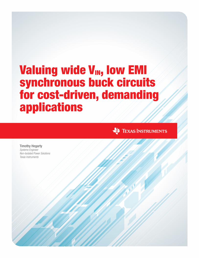
Synchronous buck converters with a wide VIN range proven EMI performance and multi-output flexibility are indispensable features to reduce total solution cost and time-to-market
At the epicenter of most power converter implementations is an inevitable trade-off of efficiency versus
solution size [1] However new applications are coming to fruition that have unique power solution
requirements tied to a number of performance features For the cost-driven industrial automotive
and communications applications shown in Figure 1 three particularly desirable features pertinent to
synchronous buck converter circuits are required 1) wide input voltage operating range or wide VIN
2) multiple outputs both non-isolated and isolated leveraging dual-channel and Fly-Bucktrade solutions
and 3) low noise and electromagnetic interference (EMI)
Referencing Texas Instruments portfolio of easy-to-use wide VIN buck converters and controllers this
white paper takes a close look at the value proposition of each listed feature as it relates to a product
development environment where bill-of-materials (BOM) cost optimization reliability and time-to-market
are the overarching constraints
Power converters specifically with wide VIN range
[2] provide an operating margin to quell input rail
transient voltage disturbances This type of transient
immunity performance is critical in applications
where high reliability or an extended product life
cycle is required
For example industrial automation and process
control equipment often must operate from largely
unregulated 8 V-to-36 V rails that also support
high current and inductive load switching of
electromechanical (EM) devices Examples include
motors relays and circuit breakers When such
Figure 1 Cost-driven demanding applications within automotive industrial and communications segments
Wide VIN operating range
Valuing wide VIN low EMI synchronous buck circuits 3 April 2019
devices switch on and off the combination of series
parasitic inductance and high slew rate currents
contribute to momentary power surges causing
voltage fluctuations and large overvoltage spikes
on the supply rail Furthermore IEC 61000-4
a common transient immunity specification for
industrial applications [3] describes low- and
high-frequency input disturbances (ESD burst
lightningsurge and conducted and radiated
immunity) Such high slew rates and high-voltage
line transients often expose the fragility or
marginality of a particular design resulting in
electrical overstress (EOS) or even catastrophic failure
A passive protection network typically consisting
of a low-pass LC filter and transient voltage
suppression (TVS) array is used as a first line of
defense to clamp the peak-voltage excursions
However the circuits located downstream from
the protection network must survive up to a 100-V
peak transient voltage without damage as well
as function seamlessly through these types of
transients without interruption
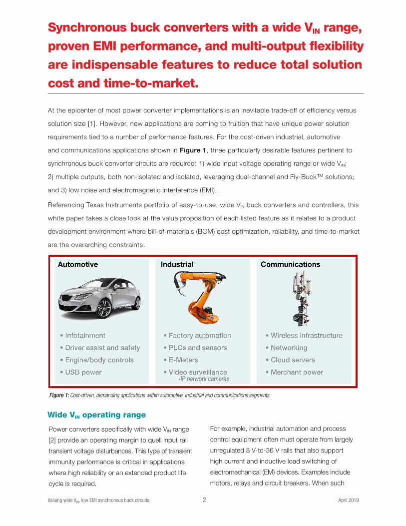
Using a DCDC converter that produces a
tightly-regulated output even in volatile voltage
environments with a wide range of dynamic
disturbances Figure 2 shows an example of a
high-efficiency solution using an emulated
current-mode (ECM) control technique specifically
intended for large step-down conversion ratios
Operating over a 161 wide VIN range and capable
of sustaining repetitive 100-V surges the converter
maintains uninterrupted regulation and the output
voltage is immune to large and noisy voltage
swings at the input The wide VIN range capability
reduces the cost of ancillary passive components
for transient protection and renders designs with
minimal component derating unnecessary
Multiple outputs
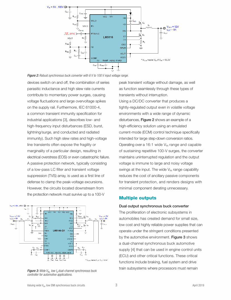
Dual output synchronous buck converter
The proliferation of electronic subsystems in
automobiles has created demand for small size
low cost and highly reliable power supplies that can
operate under the stringent conditions presented
by the automotive environment Figure 3 shows
a dual-channel synchronous buck automotive
supply [4] that can be used in engine control units
(ECU) and other critical functions These critical
functions include braking fuel system and drive
train subsystems where processors must remain
Figure 2 Robust synchronous buck converter with 6 V to 100 V input voltage range
Figure 3 Wide VIN low IQ dual-channel synchronous buck controller for automotive applications
Valuing wide VIN low EMI synchronous buck circuits 4 April 2019
powered without glitches during even the
most severe battery voltage transients
You can select a fixed switching frequency
at either 22 MHz or 440 kHz to operate
above or below the AM broadcast band
respectively with the option to synchronize
to an external clock if needed The dual-
channel controller pushes cost and size
boundaries by minimizing the solution
footprint The two channels are interleaved
180 degrees out-of-phase for lower
input ripple current with respect to two
independent single-phase converters
Dual-gate drive outputs allow you to adjust the
switch (SW) voltage and current slew rate which helps
to reduce high-frequency noise and EMI filter size
At the same time an IC package with wettable flank
terminations allow you to visually inspect the printed
circuit board (PCB) for solder joint integrity reducing
production cost and increasing reliability
Fly-Buck converter
Recently gaining prominence as a sub-20 W isolated
power solution is the Fly-Buck converter [5] As
an extension of the synchronous buck regulator
the Fly-Buck circuit lowers the solution cost by
eschewing loop compensation and feedback
optocoupler components A compensated
error amplifier is not needed and an adaptive
constant on-time (COT) control approach gives a
nearly-instantaneous response for excellent transient
dynamics For maximum flexibility both isolated and
non-isolated outputs are available The Fly-Buck
can be used for low-current auxiliary and bias rails
floating gate supplies that drive power MOSFETs
and IGBTs and bipolar supplies for powering
high-precision amplifiers and data converters
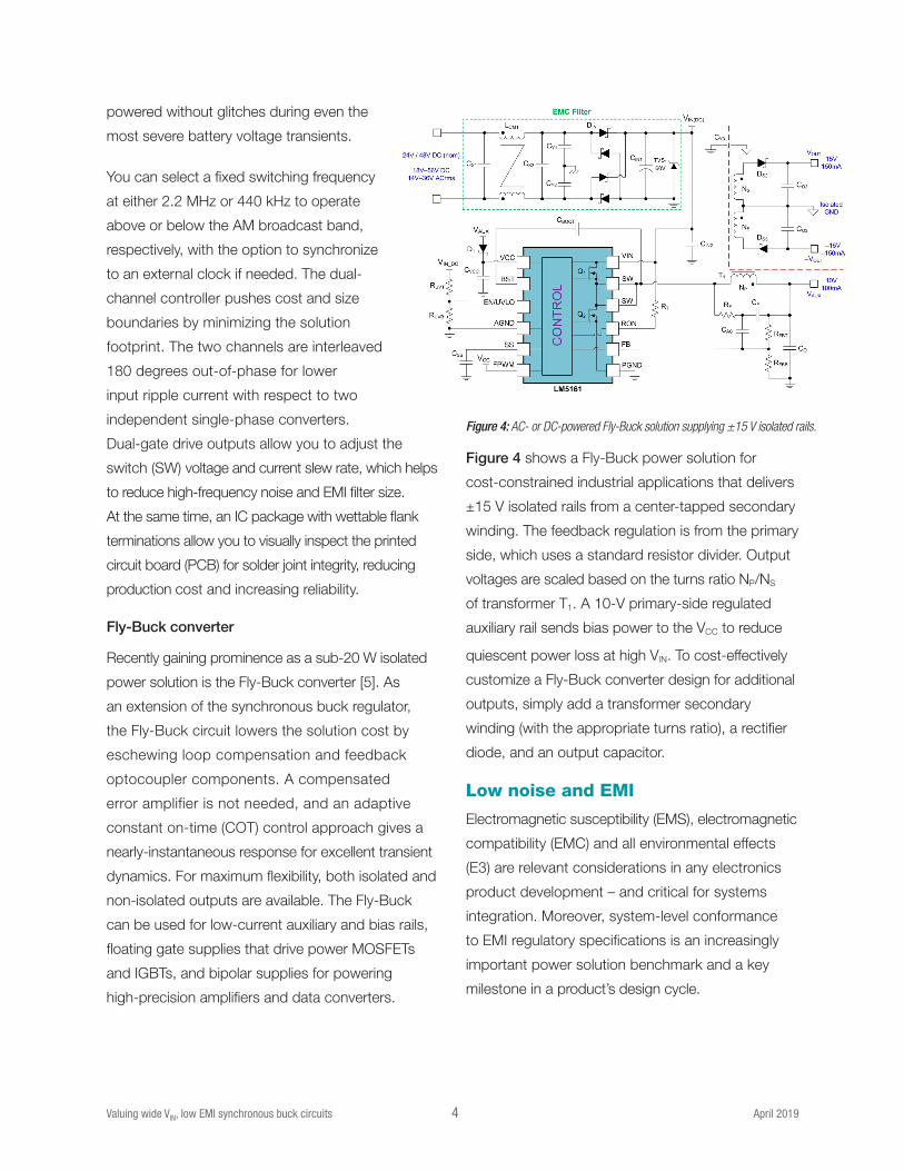
Figure 4 shows a Fly-Buck power solution for
cost-constrained industrial applications that delivers
plusmn15 V isolated rails from a center-tapped secondary
winding The feedback regulation is from the primary
side which uses a standard resistor divider Output
voltages are scaled based on the turns ratio NPNS
of transformer T1 A 10-V primary-side regulated
auxiliary rail sends bias power to the VCC to reduce
quiescent power loss at high VIN To cost-effectively
customize a Fly-Buck converter design for additional
outputs simply add a transformer secondary
winding (with the appropriate turns ratio) a rectifier
diode and an output capacitor
Low noise and EMI
Electromagnetic susceptibility (EMS) electromagnetic
compatibility (EMC) and all environmental effects
(E3) are relevant considerations in any electronics
product development ndash and critical for systems
integration Moreover system-level conformance
to EMI regulatory specifications is an increasingly
important power solution benchmark and a key
milestone in a productrsquos design cycle
Figure 4 AC- or DC-powered Fly-Buck solution supplying plusmn15 V isolated rails
Valuing wide VIN low EMI synchronous buck circuits 5 April 2019
Such strict regulatory standards have spurred
demand for proven ldquoout-of-the-boxrdquo compliant
solutions using recommended EMI filtering
components and PCB layout techniques Typically
a high-density design has little space available for
EMI filtering Fortunately a tight layout improves
radiated emissions as well as immunity to incoming
disturbances Essential steps to take are to minimize
loop areas containing high didt currents and
reduce surface areas with high dvdt voltages
(such as switch node copper polygon areas) [6-8]
Many power converter ICs are specifically designed
to minimize their EMI signature For example the
LM5088-Q1 a current-mode buck controller from
TI has an optional spread-spectrum feature that
reduces peak emission levels particularly at the
fundamental frequency and lower harmonics The
LM5140-Q1 controller presented in Figure 3 has
high-side and low-side gate drivers with adjustable
slew rate control to mitigate higher-frequency
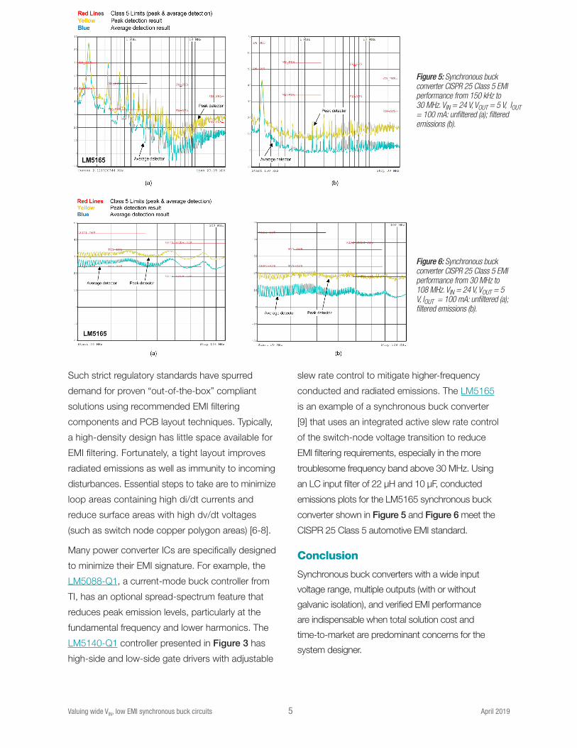
conducted and radiated emissions The LM5165
is an example of a synchronous buck converter
[9] that uses an integrated active slew rate control
of the switch-node voltage transition to reduce
EMI filtering requirements especially in the more
troublesome frequency band above 30 MHz Using
an LC input filter of 22 microH and 10 microF conducted
emissions plots for the LM5165 synchronous buck
converter shown in Figure 5 and Figure 6 meet the
CISPR 25 Class 5 automotive EMI standard
Conclusion
Synchronous buck converters with a wide input
voltage range multiple outputs (with or without
galvanic isolation) and verified EMI performance
are indispensable when total solution cost and
time-to-market are predominant concerns for the
system designer
Figure 5 Synchronous buck converter CISPR 25 Class 5 EMI performance from 150 kHz to 30 MHz VIN = 24 V VOUT = 5 V IOUT = 100 mA unfiltered (a) filtered emissions (b)
Figure 6 Synchronous buck converter CISPR 25 Class 5 EMI performance from 30 MHz to 108 MHz VIN = 24 V VOUT = 5 V IOUT = 100 mA unfiltered (a) filtered emissions (b)
References
1 Hegarty Timothy ldquoThe buck regulator efficiencysize tradeoff dilemmardquo Power House TI blog December 2 2013
2 Choudhary Vijay ldquoWide VIN power management ICs simplify design reduce BOM cost and enhance reliabilityrdquo
TI white paper September 2013
3 Hegarty Timothy ldquoWide VIN synchronous buck converter powers smart sensorsrdquo Power Electronics July 29 2016
4 Wide VIN automotive applications Texas Instruments website
5 Hegarty Timothy ldquoFly-Buck converter provides EMC and isolation in PLC applicationsrdquo Texas Instruments Analog Applications
Journal (TI AAJ) 1Q 2015
6 Hegarty Timothy High density PCB layout of DCDC convertersrdquo Power House TI blog September 16 2015
7 ldquoVertically stacked MOSFETs and other tricks for building a high-density 30-A point-of-load regulatorrdquo
How2Power March 2016
8 Hegarty Timothy ldquoReduce buck converter EMI and voltage stress by minimizing inductive parasiticsrdquo TI AAJ 3Q 2016
9 Hegarty Timothy ldquoLow-IQ synchronous buck converter enables intelligent field sensor applicationsrdquo TI AAJ 2Q 2016
10 Download these data sheets LM5088-Q1 LM5140-Q1 LM5161 LM5165
Important Notice The products and services of Texas Instruments Incorporated and its subsidiaries described herein are sold subject to TIrsquos standard terms and conditions of sale Customers are advised to obtain the most current and complete information about TI products and services before placing orders TI assumes no liability for applications assistance customerrsquos applications or product designs software performance or infringement of patents The publication of information regarding any other companyrsquos products or services does not constitute TIrsquos approval warranty or endorsement thereof
SLYY104A
Fly-Buck Type C and the platform bar are trademarks of Texas InstrumentsAll other trademarks are the property of their respective owners
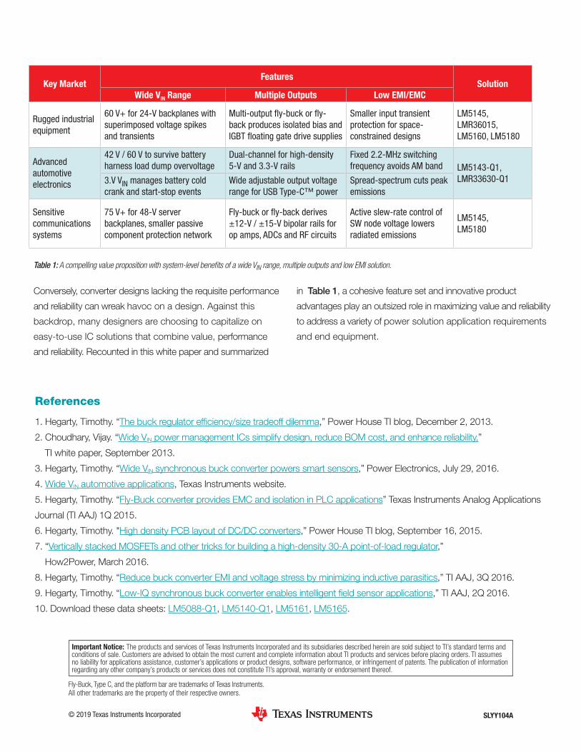
Table 1 A compelling value proposition with system-level benefits of a wide VIN range multiple outputs and low EMI solution
Conversely converter designs lacking the requisite performance
and reliability can wreak havoc on a design Against this
backdrop many designers are choosing to capitalize on
easy-to-use IC solutions that combine value performance
and reliability Recounted in this white paper and summarized
in Table 1 a cohesive feature set and innovative product
advantages play an outsized role in maximizing value and reliability
to address a variety of power solution application requirements
and end equipment
copy 2019 Texas Instruments Incorporated
Key MarketFeatures
SolutionWide VIN Range Multiple Outputs Low EMIEMC
Rugged industrialequipment
60 V+ for 24-V backplanes with superimposed voltage spikes and transients
Multi-output fly-buck or fly-back produces isolated bias and IGBT floating gate drive supplies
Smaller input transient protection for space-constrained designs
LM5145 LMR36015 LM5160 LM5180
Advanced automotiveelectronics
42 V 60 V to survive battery harness load dump overvoltage
Dual-channel for high-density 5-V and 33-V rails
Fixed 22-MHz switching frequency avoids AM band LM5143-Q1
LMR33630-Q13V VIN manages battery cold crank and start-stop events
Wide adjustable output voltage range for USB Type-Ctrade power
Spread-spectrum cuts peak emissions
Sensitive communicationssystems
75 V+ for 48-V server backplanes smaller passive component protection network
Fly-buck or fly-back derives plusmn12-V plusmn15-V bipolar rails for op amps ADCs and RF circuits
Active slew-rate control of SW node voltage lowers radiated emissions
LM5145 LM5180
IMPORTANT NOTICE AND DISCLAIMER
TI PROVIDES TECHNICAL AND RELIABILITY DATA (INCLUDING DATASHEETS) DESIGN RESOURCES (INCLUDING REFERENCEDESIGNS) APPLICATION OR OTHER DESIGN ADVICE WEB TOOLS SAFETY INFORMATION AND OTHER RESOURCES ldquoAS ISrdquoAND WITH ALL FAULTS AND DISCLAIMS ALL WARRANTIES EXPRESS AND IMPLIED INCLUDING WITHOUT LIMITATION ANYIMPLIED WARRANTIES OF MERCHANTABILITY FITNESS FOR A PARTICULAR PURPOSE OR NON-INFRINGEMENT OF THIRDPARTY INTELLECTUAL PROPERTY RIGHTSThese resources are intended for skilled developers designing with TI products You are solely responsible for (1) selecting the appropriateTI products for your application (2) designing validating and testing your application and (3) ensuring your application meets applicablestandards and any other safety security or other requirements These resources are subject to change without notice TI grants youpermission to use these resources only for development of an application that uses the TI products described in the resource Otherreproduction and display of these resources is prohibited No license is granted to any other TI intellectual property right or to any thirdparty intellectual property right TI disclaims responsibility for and you will fully indemnify TI and its representatives against any claimsdamages costs losses and liabilities arising out of your use of these resourcesTIrsquos products are provided subject to TIrsquos Terms of Sale (wwwticomlegaltermsofsalehtml) or other applicable terms available either onticom or provided in conjunction with such TI products TIrsquos provision of these resources does not expand or otherwise alter TIrsquos applicablewarranties or warranty disclaimers for TI products
Mailing Address Texas Instruments Post Office Box 655303 Dallas Texas 75265Copyright copy 2019 Texas Instruments Incorporated
Valuing wide VIN low EMI synchronous buck circuits 2 April 2019
Synchronous buck converters with a wide VIN range proven EMI performance and multi-output flexibility are indispensable features to reduce total solution cost and time-to-market
At the epicenter of most power converter implementations is an inevitable trade-off of efficiency versus
solution size [1] However new applications are coming to fruition that have unique power solution
requirements tied to a number of performance features For the cost-driven industrial automotive
and communications applications shown in Figure 1 three particularly desirable features pertinent to
synchronous buck converter circuits are required 1) wide input voltage operating range or wide VIN
2) multiple outputs both non-isolated and isolated leveraging dual-channel and Fly-Bucktrade solutions
and 3) low noise and electromagnetic interference (EMI)
Referencing Texas Instruments portfolio of easy-to-use wide VIN buck converters and controllers this
white paper takes a close look at the value proposition of each listed feature as it relates to a product
development environment where bill-of-materials (BOM) cost optimization reliability and time-to-market
are the overarching constraints
Power converters specifically with wide VIN range
[2] provide an operating margin to quell input rail
transient voltage disturbances This type of transient
immunity performance is critical in applications
where high reliability or an extended product life
cycle is required
For example industrial automation and process
control equipment often must operate from largely
unregulated 8 V-to-36 V rails that also support
high current and inductive load switching of
electromechanical (EM) devices Examples include
motors relays and circuit breakers When such
Figure 1 Cost-driven demanding applications within automotive industrial and communications segments
Wide VIN operating range
Valuing wide VIN low EMI synchronous buck circuits 3 April 2019
devices switch on and off the combination of series
parasitic inductance and high slew rate currents
contribute to momentary power surges causing
voltage fluctuations and large overvoltage spikes
on the supply rail Furthermore IEC 61000-4
a common transient immunity specification for
industrial applications [3] describes low- and
high-frequency input disturbances (ESD burst
lightningsurge and conducted and radiated
immunity) Such high slew rates and high-voltage
line transients often expose the fragility or
marginality of a particular design resulting in
electrical overstress (EOS) or even catastrophic failure
A passive protection network typically consisting
of a low-pass LC filter and transient voltage
suppression (TVS) array is used as a first line of
defense to clamp the peak-voltage excursions
However the circuits located downstream from
the protection network must survive up to a 100-V
peak transient voltage without damage as well
as function seamlessly through these types of
transients without interruption
Using a DCDC converter that produces a
tightly-regulated output even in volatile voltage
environments with a wide range of dynamic
disturbances Figure 2 shows an example of a
high-efficiency solution using an emulated
current-mode (ECM) control technique specifically
intended for large step-down conversion ratios
Operating over a 161 wide VIN range and capable
of sustaining repetitive 100-V surges the converter
maintains uninterrupted regulation and the output
voltage is immune to large and noisy voltage
swings at the input The wide VIN range capability
reduces the cost of ancillary passive components
for transient protection and renders designs with
minimal component derating unnecessary
Multiple outputs
Dual output synchronous buck converter
The proliferation of electronic subsystems in
automobiles has created demand for small size
low cost and highly reliable power supplies that can
operate under the stringent conditions presented
by the automotive environment Figure 3 shows
a dual-channel synchronous buck automotive
supply [4] that can be used in engine control units
(ECU) and other critical functions These critical
functions include braking fuel system and drive
train subsystems where processors must remain
Figure 2 Robust synchronous buck converter with 6 V to 100 V input voltage range
Figure 3 Wide VIN low IQ dual-channel synchronous buck controller for automotive applications
Valuing wide VIN low EMI synchronous buck circuits 4 April 2019
powered without glitches during even the
most severe battery voltage transients
You can select a fixed switching frequency
at either 22 MHz or 440 kHz to operate
above or below the AM broadcast band
respectively with the option to synchronize
to an external clock if needed The dual-
channel controller pushes cost and size
boundaries by minimizing the solution
footprint The two channels are interleaved
180 degrees out-of-phase for lower
input ripple current with respect to two
independent single-phase converters
Dual-gate drive outputs allow you to adjust the
switch (SW) voltage and current slew rate which helps
to reduce high-frequency noise and EMI filter size
At the same time an IC package with wettable flank
terminations allow you to visually inspect the printed
circuit board (PCB) for solder joint integrity reducing
production cost and increasing reliability
Fly-Buck converter
Recently gaining prominence as a sub-20 W isolated
power solution is the Fly-Buck converter [5] As
an extension of the synchronous buck regulator
the Fly-Buck circuit lowers the solution cost by
eschewing loop compensation and feedback
optocoupler components A compensated
error amplifier is not needed and an adaptive
constant on-time (COT) control approach gives a
nearly-instantaneous response for excellent transient
dynamics For maximum flexibility both isolated and
non-isolated outputs are available The Fly-Buck
can be used for low-current auxiliary and bias rails
floating gate supplies that drive power MOSFETs
and IGBTs and bipolar supplies for powering
high-precision amplifiers and data converters
Figure 4 shows a Fly-Buck power solution for
cost-constrained industrial applications that delivers
plusmn15 V isolated rails from a center-tapped secondary
winding The feedback regulation is from the primary
side which uses a standard resistor divider Output
voltages are scaled based on the turns ratio NPNS
of transformer T1 A 10-V primary-side regulated
auxiliary rail sends bias power to the VCC to reduce
quiescent power loss at high VIN To cost-effectively
customize a Fly-Buck converter design for additional
outputs simply add a transformer secondary
winding (with the appropriate turns ratio) a rectifier
diode and an output capacitor
Low noise and EMI
Electromagnetic susceptibility (EMS) electromagnetic
compatibility (EMC) and all environmental effects
(E3) are relevant considerations in any electronics
product development ndash and critical for systems
integration Moreover system-level conformance
to EMI regulatory specifications is an increasingly
important power solution benchmark and a key
milestone in a productrsquos design cycle
Figure 4 AC- or DC-powered Fly-Buck solution supplying plusmn15 V isolated rails
Valuing wide VIN low EMI synchronous buck circuits 5 April 2019
Such strict regulatory standards have spurred
demand for proven ldquoout-of-the-boxrdquo compliant
solutions using recommended EMI filtering
components and PCB layout techniques Typically
a high-density design has little space available for
EMI filtering Fortunately a tight layout improves
radiated emissions as well as immunity to incoming
disturbances Essential steps to take are to minimize
loop areas containing high didt currents and
reduce surface areas with high dvdt voltages
(such as switch node copper polygon areas) [6-8]
Many power converter ICs are specifically designed
to minimize their EMI signature For example the
LM5088-Q1 a current-mode buck controller from
TI has an optional spread-spectrum feature that
reduces peak emission levels particularly at the
fundamental frequency and lower harmonics The
LM5140-Q1 controller presented in Figure 3 has
high-side and low-side gate drivers with adjustable
slew rate control to mitigate higher-frequency
conducted and radiated emissions The LM5165
is an example of a synchronous buck converter
[9] that uses an integrated active slew rate control
of the switch-node voltage transition to reduce
EMI filtering requirements especially in the more
troublesome frequency band above 30 MHz Using
an LC input filter of 22 microH and 10 microF conducted
emissions plots for the LM5165 synchronous buck
converter shown in Figure 5 and Figure 6 meet the
CISPR 25 Class 5 automotive EMI standard
Conclusion
Synchronous buck converters with a wide input
voltage range multiple outputs (with or without
galvanic isolation) and verified EMI performance
are indispensable when total solution cost and
time-to-market are predominant concerns for the
system designer
Figure 5 Synchronous buck converter CISPR 25 Class 5 EMI performance from 150 kHz to 30 MHz VIN = 24 V VOUT = 5 V IOUT = 100 mA unfiltered (a) filtered emissions (b)
Figure 6 Synchronous buck converter CISPR 25 Class 5 EMI performance from 30 MHz to 108 MHz VIN = 24 V VOUT = 5 V IOUT = 100 mA unfiltered (a) filtered emissions (b)
References
1 Hegarty Timothy ldquoThe buck regulator efficiencysize tradeoff dilemmardquo Power House TI blog December 2 2013
2 Choudhary Vijay ldquoWide VIN power management ICs simplify design reduce BOM cost and enhance reliabilityrdquo
TI white paper September 2013
3 Hegarty Timothy ldquoWide VIN synchronous buck converter powers smart sensorsrdquo Power Electronics July 29 2016
4 Wide VIN automotive applications Texas Instruments website
5 Hegarty Timothy ldquoFly-Buck converter provides EMC and isolation in PLC applicationsrdquo Texas Instruments Analog Applications
Journal (TI AAJ) 1Q 2015
6 Hegarty Timothy High density PCB layout of DCDC convertersrdquo Power House TI blog September 16 2015
7 ldquoVertically stacked MOSFETs and other tricks for building a high-density 30-A point-of-load regulatorrdquo
How2Power March 2016
8 Hegarty Timothy ldquoReduce buck converter EMI and voltage stress by minimizing inductive parasiticsrdquo TI AAJ 3Q 2016
9 Hegarty Timothy ldquoLow-IQ synchronous buck converter enables intelligent field sensor applicationsrdquo TI AAJ 2Q 2016
10 Download these data sheets LM5088-Q1 LM5140-Q1 LM5161 LM5165
Important Notice The products and services of Texas Instruments Incorporated and its subsidiaries described herein are sold subject to TIrsquos standard terms and conditions of sale Customers are advised to obtain the most current and complete information about TI products and services before placing orders TI assumes no liability for applications assistance customerrsquos applications or product designs software performance or infringement of patents The publication of information regarding any other companyrsquos products or services does not constitute TIrsquos approval warranty or endorsement thereof
SLYY104A
Fly-Buck Type C and the platform bar are trademarks of Texas InstrumentsAll other trademarks are the property of their respective owners
Table 1 A compelling value proposition with system-level benefits of a wide VIN range multiple outputs and low EMI solution
Conversely converter designs lacking the requisite performance
and reliability can wreak havoc on a design Against this
backdrop many designers are choosing to capitalize on
easy-to-use IC solutions that combine value performance
and reliability Recounted in this white paper and summarized
in Table 1 a cohesive feature set and innovative product
advantages play an outsized role in maximizing value and reliability
to address a variety of power solution application requirements
and end equipment
copy 2019 Texas Instruments Incorporated
Key MarketFeatures
SolutionWide VIN Range Multiple Outputs Low EMIEMC
Rugged industrialequipment
60 V+ for 24-V backplanes with superimposed voltage spikes and transients
Multi-output fly-buck or fly-back produces isolated bias and IGBT floating gate drive supplies
Smaller input transient protection for space-constrained designs
LM5145 LMR36015 LM5160 LM5180
Advanced automotiveelectronics
42 V 60 V to survive battery harness load dump overvoltage
Dual-channel for high-density 5-V and 33-V rails
Fixed 22-MHz switching frequency avoids AM band LM5143-Q1
LMR33630-Q13V VIN manages battery cold crank and start-stop events
Wide adjustable output voltage range for USB Type-Ctrade power
Spread-spectrum cuts peak emissions
Sensitive communicationssystems
75 V+ for 48-V server backplanes smaller passive component protection network
Fly-buck or fly-back derives plusmn12-V plusmn15-V bipolar rails for op amps ADCs and RF circuits
Active slew-rate control of SW node voltage lowers radiated emissions
LM5145 LM5180
IMPORTANT NOTICE AND DISCLAIMER
TI PROVIDES TECHNICAL AND RELIABILITY DATA (INCLUDING DATASHEETS) DESIGN RESOURCES (INCLUDING REFERENCEDESIGNS) APPLICATION OR OTHER DESIGN ADVICE WEB TOOLS SAFETY INFORMATION AND OTHER RESOURCES ldquoAS ISrdquoAND WITH ALL FAULTS AND DISCLAIMS ALL WARRANTIES EXPRESS AND IMPLIED INCLUDING WITHOUT LIMITATION ANYIMPLIED WARRANTIES OF MERCHANTABILITY FITNESS FOR A PARTICULAR PURPOSE OR NON-INFRINGEMENT OF THIRDPARTY INTELLECTUAL PROPERTY RIGHTSThese resources are intended for skilled developers designing with TI products You are solely responsible for (1) selecting the appropriateTI products for your application (2) designing validating and testing your application and (3) ensuring your application meets applicablestandards and any other safety security or other requirements These resources are subject to change without notice TI grants youpermission to use these resources only for development of an application that uses the TI products described in the resource Otherreproduction and display of these resources is prohibited No license is granted to any other TI intellectual property right or to any thirdparty intellectual property right TI disclaims responsibility for and you will fully indemnify TI and its representatives against any claimsdamages costs losses and liabilities arising out of your use of these resourcesTIrsquos products are provided subject to TIrsquos Terms of Sale (wwwticomlegaltermsofsalehtml) or other applicable terms available either onticom or provided in conjunction with such TI products TIrsquos provision of these resources does not expand or otherwise alter TIrsquos applicablewarranties or warranty disclaimers for TI products
Mailing Address Texas Instruments Post Office Box 655303 Dallas Texas 75265Copyright copy 2019 Texas Instruments Incorporated