Embed Size (px)
Citation preview
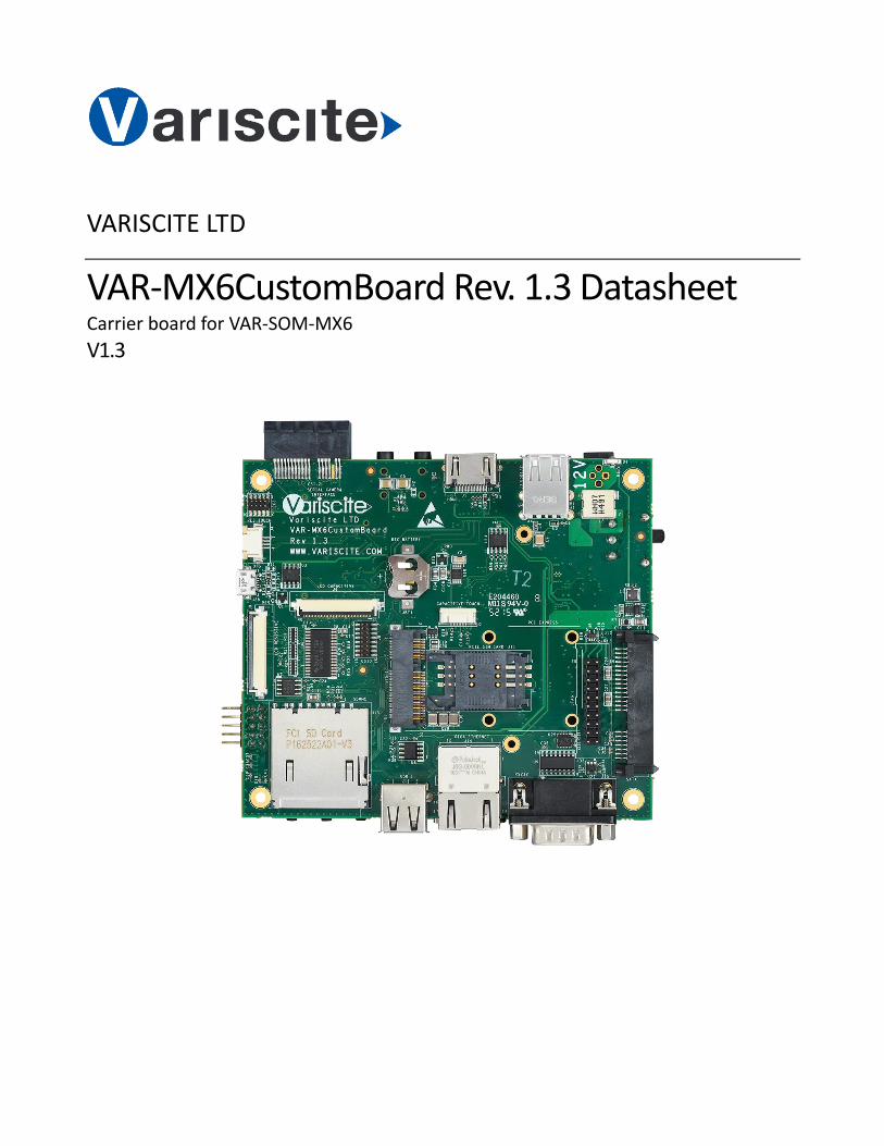
VARISCITE LTD
VAR-MX6CustomBoard Rev. 1.3 Datasheet Carrier board for VAR-SOM-MX6 V1.3
© 2016 Variscite Ltd. All Rights Reserved. No part of this document may be photocopied, reproduced, stored in a retrieval system, or transmitted, in any form or by any means whether, electronic, mechanical, or otherwise without the prior written permission of Variscite Ltd. No warranty of accuracy is given concerning the contents of the information contained in this publication. To the extent permitted by law no liability (including liability to any person by reason of negligence) will be accepted by Variscite Ltd., its subsidiaries or employees for any direct or indirect loss or damage caused by omissions from or inaccuracies in this document. Variscite Ltd. reserves the right to change details in this publication without notice. Product and company names herein may be the trademarks of their respective owners. Variscite Ltd. 4, Hamelacha Street Lod 71520 Israel

Revision History
Revision Date Notes
1.0 30/07/2012 Initial
1.1 19/12/2012 DSI connector pin-out fixed LVDS connector changed USB OTG connector Reference Designator changed MIPI CSI-2 connector pin-out changed Top view picture changed
1.2 21/01/2016 Corrected Table 2-28 connector RefDes Corrected RS232 (J15, J34) pinout table

Table of ContentsRevision History ............................................................................................................................... iii
Table of Contents ............................................................................................................................. iv
List of Tables .....................................................................................................................................6
1 Overview ..............................................................................................................................7
1.1 General Information ............................................................................................................7
1.2 Additional Information ........................................................................................................7
1.3 VAR-MX6CustomBoard Features Summary: .......................................................................8
1.4 Block Diagram ......................................................................................................................9
1.5 Board Layout ..................................................................................................................... 10
1.6 VAR-MX6CustomBoard Connectors ................................................................................. 11
2 Detailed Description ......................................................................................................... 12
2.1 Overview ........................................................................................................................... 12
2.2 VAR-SOM-MX6 Interfaces................................................................................................. 13
2.2.1 SO-DIMM 200 (J18) ........................................................................................................... 13
2.3 Standard External Interfaces ............................................................................................ 13
2.3.1 HDMI Connector (J1) ......................................................................................................... 13
2.3.2 HOST USB (J3, J16) ............................................................................................................ 14
2.3.3 USB OTG (J38) ................................................................................................................... 14
2.3.4 Mini PCIe (J10) .................................................................................................................. 15
2.3.5 USIM Card (J11) ................................................................................................................ 17
2.3.6 SATA (J12) ......................................................................................................................... 17
2.3.7 SD Card (J13) ..................................................................................................................... 18
2.3.8 Ethernet (J14) .................................................................................................................... 19
2.3.9 RS232 – DTE (J15).............................................................................................................. 20
2.3.10 AUDIO (J20, J21) ................................................................................................................ 20
2.3.11 RS232 – Terminal (J34)...................................................................................................... 21
2.4 DVK External Interfaces .................................................................................................... 22
2.4.1 SOM Expansion (J30) ........................................................................................................ 22

2.4.2 LCD (J9/J6) ......................................................................................................................... 26
2.4.3 Touch panel (J7) ................................................................................................................ 28
2.4.4 Backlight power supply connector (J23)[1] ........................................................................ 29
2.4.5 LVDS Interface Connector (J22) ........................................................................................ 29
2.4.6 Parallel Camera Interface (J8) ........................................................................................... 30
2.4.7 SD/MMC1 (J32) ................................................................................................................. 30
2.4.8 AUDIO (J37) ....................................................................................................................... 31
2.4.9 CAN1, UART2 (RS485) & DMIC Interface (J26, J35) .......................................................... 31
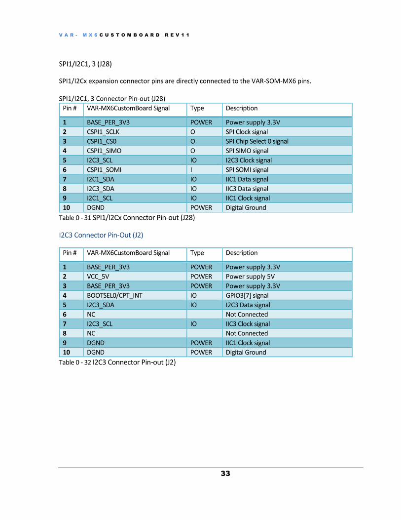
2.4.10 SPI1/I2C1, 3 (J28) .............................................................................................................. 33
2.4.11 DSI (J24) ............................................................................................................................ 34
2.4.12 CSI2 Camera (J17) ............................................................................................................. 34
2.5 User Interfaces .................................................................................................................. 35
2.5.1 LED Indications .................................................................................................................. 35
2.5.2 Control Buttons ................................................................................................................. 36
2.5.3 Power Input (J18/J19) ....................................................................................................... 36
2.6 Absolute Maximum Electrical Specifications .................................................................... 38
2.7 Operational Electrical Specifications ................................................................................ 38
3 Legal Notice ...................................................................................................................... 39
4 Warranty Terms ................................................................................................................ 39
5 Contact Information ......................................................................................................... 41

V A R - M X 6 C U S T O M B O A R D R E V 1 1
6
List of Tables Table 1 - 1 VAR-MX6CustomBoard Connectors ................................................................ 12
Table 2 - 1 USB Host1/2 Connector Connector Pin-out (J3) ............................................. 13
Table 2 - 2 USB Host1/2 Connector Connector Pin-out (J3) ............................................. 14
Table 2 - 3 USB Host1/2 Connector Connector Pin-out (J16) ........................................... 14
Table 2 - 4 USB OTG Connector Pin-out (J38) ................................................................... 14
Table 2 – 5 Mini PCI Express Connector Pin-out (J10) ...................................................... 16
Table 2 – 6 USIM Card Connector Pin-out (J11) ............................................................... 17
Table 2 – 7 SATA Connector Pin-out (J12) ........................................................................ 18
Table 2 - 8 SD Card Slot Connector Pin-out (J13) .............................................................. 18
Table 2 - 9 1G RJ45 Connector Pin-out (J14)..................................................................... 19
Table 2 - 10 RS232 DTE Connector Pin-out (J15) .............................................................. 20
Table 2 - 11 Headphone Jack Connector Pin-out (J20) ..................................................... 20
Table 2 - 12 Line In Jack Connector Pin-out (J21) ............................................................. 21
Table 2 - 13 RS232 – Terminal Connector Pin-out (J34) ................................................... 21
Table 2 –14 SOM expansion Connector Pin-out (J30) ...................................................... 23
Table 2 –15 EMI 0 Connector Pin-out (J27) ...................................................................... 23
Table 2 –16 EMI 1 Connector Pin-out (J29) ...................................................................... 24
Table 2 –17 EMI 2 Connector Pin-out (J31) ...................................................................... 24
Table 2 –18 EMI 3 Connector Pin-out (J36) ...................................................................... 24
Table 2 –19 JTAG Connector Pin-out (J33)........................................................................ 25
Table 2 - 20 Resistive LCD Connector Pin-out (J9) ............................................................ 27
Table 2 –21 Capacitive LCD Connector Pin-out (J6) .......................................................... 28
Table 2 - 22 Capacitive Touch panel Connector Pin-out (J7) ............................................ 28
Table 2 - 23 Resistive Touch panel Connector Pin-out (J4) .............................................. 28
Table 2 –24 Backlight power supply Connector Pin-out (J23) .......................................... 29
Table 2 - 25 LVDS Connector Connector Pin-out (J22) ..................................................... 30
Table 2 - 26 Parallel camera Connector Pin-out (J8) ........................................................ 30
Table 2 - 27 SD/MMC1 Header Pin-out (J32) .................................................................... 31
Table 2 - 28 Audio Connector Pin-out (J37) ..................................................................... 31 Table 2 - 29 CAN, RS422/485 Pin-out (J26) ....................................................................... 32
Table 2 - 30 Miscellaneous Connector Pin-out (J35) ........................................................ 32
Table 2 - 31 SPI1/I2Cx Connector Pin-out (J28) ................................................................ 33
Table 2 - 32 I2C3 Connector Pin-out (J2) .......................................................................... 33
Table 2 - 33 DSI Connector Pin-out (J24) .......................................................................... 34
Table 2 - 34 CSI2 Camera Connector Pin-out (J17) ........................................................... 35
Table 2 - 35 Boot Select Switch Modes ............................................................................. 36
Table 2 - 36 Terminal Block Connector Pin-out (J19) ....................................................... 36
Table 2 - 37 Absolute Maximum Electrical Specifications ................................................ 38
Table 2 - 38 Operational Electrical Specifications ............................................................. 38

V A R - M X 6 C U S T O M B O A R D R E V 1 1
7
Overview This chapter gives a general overview of the VAR-MX6CustomBoard.
General Information
The VAR-MX6CustomBoard is a single board-computer, utilizing all the VAR-SOM-MX6 System-on-Module features. For development and production, the VAR-MX6CustomBoard serves both as a complete development kit and as an end-product, assembled according to your specifications at an optimized price-point.
• VAR-MX6CustomBoard – evaluation board
✓ Carrier -Board, compatible with VAR-SOM-MX6
✓ Schematics
• VAR-EXT-CB402 – SCI2 Camera module
• O.S support
✓ Linux BSP
✓ Windows Embedded Compact 7
✓ Android
Additional Information
Board schematics as well as a mechanical CAD data base are available for download from:
www.variscite.com.
For further information contact Variscite support at: [email protected].

V A R - M X 6 C U S T O M B O A R D R E V 1 1
8
VAR-MX6CustomBoard Features Summary:
• SO-DIMM200 socket, compatible with the VAR-SOM-MX6
• Display:
• 2x 18 Bit LCD FPC/FFC (Supporting Capacitive/Resistive modules)
• 18/24 bit LVDS Header
• MIPI DSI Header
• HDMI Type A Jack
• Resistive and Capacitive touch interface
• Backlight Driver
• Gigabit Ethernet Port , RJ45
• USB: OTG Mini-AB, Type A HOST X 3
• SATA Connector
• SD-Card
• DS1337 RTC
• 36 pin PCIe (V2.0) Socket
• AUDIO: Line out, Line In ,
• RS232
• Extension Headers
• EIM , JTAG, Camera, CAN ,UART1,2 ,SPI , I2C
• 12V Power Supply , RTC Coin Backup Battery socket

V A R - M X 6 C U S T O M B O A R D R E V 1 1
9
Block Diagram

V A R - M X 6 C U S T O M B O A R D R E V 1 1
10
Board Layout
The VAR-MX6CustomBoard’s physical dimensions:
Detailed CAD files are available for download from: www.variscite.com.
Top Side - Detailed View

V A R - M X 6 C U S T O M B O A R D R E V 1 1
11
VAR-MX6CustomBoard Connectors
The table below lists all available connectors on the VAR-MX6CustomBoard - refer to Chapter 2 for detailed description and the pin-out of each connector.
Ref Function Type
J1 HDMI Connector CON RCPT HDMI TYPE A R/A SMD
J2 I2C3, Bootsel0/CPT_INT Header 5 x 2, 1.27 mm
J3 USB Host, Ports 1/2 2 x USB TYPE A
J4 Touch Panel I/F Resistive FFC/FPC 4-pin
J6 18-bit RGB LCD with Capacitive Touch
FFC/FPC 40-pin
J7 Capacitive Touch Panel I/F FFC/FPC 10-pin
J8 Camera Interface Header, 8 x 2, 1.27 mm
J9 18-bit RGB LCD with Resistive Touch FFC/FPC 40-pin
J10 Mini PCIe CON 2X26 MINI PCIe
J11 Usim Card CON 6 SIM CARD
J12 SATA SATA connector Receptacle15+7
J13 MMC-SD Card SDCARD Socket
J14 1Gb Ethernet RJ-45 1GB G/Y Led
J15 RS232 CONN DB9 (male)
J16 USB Host USB TYPE A
J17 Camera CON PCIE 36 Pin
J18 VCC-IN Con. TH. Power 4A (Option)
J19 VCC-IN Power Jack (DC Terminal)
J20 Head Phone out Audio Jack 3.5 mm
J21 Line In Audio Jack 3.5 mm
J22 LVDS Connector 40 pin LVDS cable connector
J23 LCD Backlight CON 2 PIN Crimp Style
J24 DSI Header, 5 x 2, 1.27 mm SMT
J25 VAR-SOM-MX6 DIMM200
J26 CAN Header, 5x2, 1.27 mm SMT
J27 EMI 0 Header, 5x2, 1.27 mm SMT
J28 I2C1/CSPI1 Header, 5x2, 1.27 mm SMT
J29 EMI 1 Header, 5x2, 1.27 mm SMT
J30 SOM Expansion FFC/FPC 40-pin
J31 EMI 2 Header, 5x2, 1.27 mm SMT

V A R - M X 6 C U S T O M B O A R D R E V 1 1
12
Ref Function Type
J32 SD/MMC Header, 5x2, 1.27 mm SMT
J33 JTAG Connector Header, 10 x 2, 1.27 mm TH
J34 UART1 Header, 5x2, 1.27 mm SMT RA
J35 UART2/DMIC Header, 5x2, 1.27 mm SMT
J36 EMI 3 Header, 5x2, 1.27 mm SMT
J37 Digital Audio AudMUX 4/SPDIF Header, 5x2, 1.27 mm SMT
J38 USB OTG USB Connector MINI AB
JBT1 RTC BACKUP BAT Holder CR1225
Table 0 - 1 VAR-MX6CustomBoard Connectors
Detailed Description
Overview
This chapter details the VAR-MX6CustomBoard features and external interfaces, most are driven by the VAR-SOM-MX6. Please refer to the VAR-SOM-MX6 data sheet for more information regarding those interfaces.
The following list describes this chapter’s table column header:
Pin#: Pin number of the specific connector VAR-MX6CustomBoard Signal: VAR-MX6CustomBoard schematic signal name Type: Pin Type & Direction:
• I – In
• O – Out
• DS – Differential Signal
• A – Analog
Description: Short pin functionality description

V A R - M X 6 C U S T O M B O A R D R E V 1 1
13
VAR-SOM-MX6 Interfaces
SO-DIMM 200 (J18)
The VAR-MX6CustomBoard features an SO-DIMM200 1.8 V standard connector compatible with the VAR-SOM-MX6 System-on-Module devices. Please refer to the VAR-SOM-MX6 module data- sheet for complete signals' description and pin-out.
Standard External Interfaces
HDMI Connector (J1)
The VAR-MX6CustomBoard features a standard HDMI output connector J1.
HDMI Connector Pin-out (J1)
Pin # VAR-MX6CustomBoard Signal Type Description
1 DAT2+ ODS HDMI Data 2 Positive
2 DAT2_S POWER HDMI Data 2 Shield
3 DAT2- ODS HDMI Data 2 Negative
4 DAT1+ ODS HDMI Data 1 Positive
5 DAT1_S POWER HDMI Data 1 Shield
6 DAT1- ODS HDMI Data 1 Negative
7 DAT0+ ODS HDMI Data 0 Positive
8 DAT0_S POWER HDMI Data 0 Shield
9 DAT0- ODS HDMI Data 0 Negative
10 CLK+ ODS HDMI Clock Positive
11 CLK_S POWER HDMI Clock Shield
12 CLK- ODS HDMI Clock Negative
13 CEC IO One Wire control interface
14 NC
15 SCL IO I2C HDMI interface connected to I2C2
16 SDA IO I2C HDMI interface connected to I2C2
17 DDC/CEC GND POWER One Wire control reference pin
18 +5V POWER 5V power supply
19 DET I HDMI Hot plug Detect input
Table 0 - 1 USB Host1/2 Connector Connector Pin-out (J3)

V A R - M X 6 C U S T O M B O A R D R E V 1 1
14
HOST USB (J3, J16)
The VAR-MX6CustomBoard supports three USB 2.0 host ports. All are driven by an on-board USB hub.
USB Host 1/2 Connector Pin-out (J3)
Pin # VAR-MX6CustomBoard Signal Type Description
A1 VCC_USB1 Power 5 V power supply,500 mA max.
A2 USB_HUB_DN1 DSI/O USB data negative
A3 USB_HUB_DP1 DSI/O USB data positive
A4 GND Power Digital Ground
B1 VCC_USB2 Power 5 V power supply, 500 mA max.
B2 USB_HUB_DN2 DSI/O USB data negative
B3 USB_HUB_DP2 DSI/O USB data positive
B4 GND Power Digital Ground
Table 0 - 2 USB Host1/2 Connector Connector Pin-out (J3)
USB Host Connector Pin-out (J16)
Pin # VAR-MX6CustomBoard Signal Type Description
1 VCC_USB3 Power 5 V power supply, 500 mA max.
2 USB_HUB_DN3 DSI/O USB data negative
3 USB_HUB_DP3 DSI/O USB data positive
4 GND Power Digital Ground
Table 0 - 3 USB Host1/2 Connector Connector Pin-out (J16)
USB OTG (J38)
The VAR-MX6CustomBoard OTG is driven by the VAR-SOM-MX6 OTG interface.
USB OTG Connector Pin-out (J38)
Pin # VAR-MX6CustomBoard Signal Type Description
1 OTG_VBUS Power 5 V in/out (client/host)
2 USB_OTG_DM DSI/O USB data minus
3 USB_OTG_DP DSI/O USB data plus
4 USB_OTG_ID I USB OTG ID signal (‘1’ - device mode)
5 DGND Power Digital Ground
Table 0 - 4 USB OTG Connector Pin-out (J38)

V A R - M X 6 C U S T O M B O A R D R E V 1 1
15
Mini PCIe (J10)
The VAR-MX6Custom Board Mini PCI Express interface is exposed by a standard Mini PCI Express connector. Mini PCI Express port is directly connected to the VAR-SOM-MX6 as well as to USIM socket (J11), supporting PCIe modems.
Mini PCIe Connector Pin-out (J10)
Pin # VAR-MX6CustomBoard Signal Type Description
1 SPDIF_OUT_PCIE_PCIE_WAKE_B
2 BASE_PER_3V3 POWER 3.3V power supply
3 NC Not Connected
4 DGND POWER Digital Ground
5 NC Not Connected
6 VCC_1V5_PCIE POWER 1.5V power supply limited to 300mA
7 NC Not Connected
8 PCIE_UIM_PWR O SIM Card VCC power supply
9 DGND POWER Digital Ground
10 PCIE_UIM_DATA IO SIM Card data
11 PCIE_REFCLKM DSO PCIE Clock pair negative
12 PCI3_UIM_CLK O SIM Card clock
13 PCIE_REFCLKP DSO PCIE Clock pair positive
14 PCIE_UIM_RST O SIM Card reset
15 DGND POWER Digital Ground
16 PCIE_UIM_VPP O SIM Card VPP power supply
17 NC Not Connected
18 DGND POWER Digital Ground
19 NC Not Connected
20 SPDIF_IN_PCIE_DIS_B O Disable signal
21 DGND POWER Digital Ground
22 AUDMUX4_RXC_PCIE_RESET_B O Reset signal
23 PCIE_RXM DSI PCIE Receive pair negative
24 BASE_PER_3V3 POWER 3.3V power supply
25 PCIE_RXP DSI PCIE Receive pair positive
26 DGND POWER Digital Ground
27 DGND POWER Digital Ground
28 VCC_1V5_PCIE POWER 1.5V power supply limited to 300mA
29 DGND POWER Digital Groung
30 I2C3_SCL IO I2C3 Clock
31 PCIE_TXM DSO PCIE Transmit pair negative
32 I2C3_SDA IO I2C3 Data
33 PCIE_TXP DSO PCIE Transmit pair positive

V A R - M X 6 C U S T O M B O A R D R E V 1 1
16
Pin # VAR-MX6CustomBoard Signal Type Description
34 DGND POWER Digital Ground
35 DGND POWER Digital Ground
36 USB_HUB_DN4 DSIO USB data minus
37 DGND POWER Digital Ground
38 USB_HUB_DP4 DSIO USB data plus
39 BASE_PER_3V3 POWER 3.3V power supply
40 DGND POWER Digital Ground
41 BASE_PER_3V3 POWER 3.3V power supply
42 LED_WWAN_B I WWAN LED input
43 DGND POWER Digital Ground
44 LED_WLAN_B I WLAN LED input
45 NC Not Connected
46 LED_WPAN_B I WPAN LED input
47 NC Not Connected
48 VCC_1V5_PCIE POWER 1.5V power supply limited to 300mA
49 NC Not Connected
50 DGND POWER Digital Ground
51 NC Not Connected
52 BASE_PER_3V3 POWER 3.3V power supply
Table 0 – 5 Mini PCI Express Connector Pin-out (J10)

V A R - M X 6 C U S T O M B O A R D R E V 1 1
17
USIM Card (J11)
The VAR-MX6CustomBoard has an on-board USIM slot connected to the Mini PCI Express interface.
USIM Card Connector Pin-out (J11)
Pin # VAR-MX6CustomBoard Signal Type Description
1 VCC POWER USIM power supply
2 RESET O USIM Reset
3 CLK O USIM Clock
4 GND POWER Digital Ground
5 VPP POWER USIM Programming power supply
6 I/O IO USIM Data
Table 0 – 6 USIM Card Connector Pin-out (J11)
SATA (J12)
The VAR-MX6CustomBoard provides SATA signals & power supply through a standard 22 (7+5) pins female SATA connector (J120).
SATA Connector Pin-out (J12)
Pin # VAR-MX6CustomBoard Signal Type Description
P1 V33 POWER 3.3V power supply
P2 V33 POWER 3.3V power supply
P3 V33/PC POWER 3.3V power supply
P4 GND POWER Digital Ground
P5 GND POWER Digital Ground
P6 GND POWER Digital Ground
P7 V5/PC POWER 5V power supply
P8 V5 POWER 5V power supply
P9 V5 POWER 5V power supply
P10 GND POWER Digital Ground
P11 DAS/DSS POWER Connected to Digital Ground
P12 GND POWER Digital Ground
P13 V12/PC POWER 12V power supply (unconnected)
P14 V12 POWER 12V power supply (unconnected)
P15 V12 POWER 12V power supply (unconnected)
S1 GND POWER Digital Ground
S2 TXP ODS SATA Transmit pair positive
S3 TXN ODS SATA Transmit pair negative
S4 GND POWER Digital Ground
S5 RXN IDS SATA Receive pair negative

V A R - M X 6 C U S T O M B O A R D R E V 1 1
18
Pin # VAR-MX6CustomBoard Signal Type Description
S6 RXP IDS SATA Receive pair positive
S7 GND POWER Digital Ground
Table 0 – 7 SATA Connector Pin-out (J12)
SD Card (J13)
The SD card interface is driven by the VAR-SOM-MX6 SD/MMC0 interface. SD Card Slot Connector Pin-out (J13)
Pin # VAR-MX6CustomBoard Signal Type Description
1 SDMMC2_DAT3 DSI/O SD data 3
2 SDMMC2_CMD DSI/O SD command
3 DGND Power Digital Ground
4 VCC_SD Power SD card VCC
5 SDMMC2_CLK O SD clock
6 DGND Power Digital Ground
7 SDMMC2_DAT0 DSI/O SD data 0
8 SDMMC2_DAT1 DSI/O SD data 1
9 SDMMC2_DAT2 DSI/O SD data 2
10 SDMMC2_CD_CAN2_TX I SD card detect
11 SD_WP_CAN2_RX I SD write protected
12 DGND Power Digital Ground
13 DGND Power Digital Ground
Table 0 - 8 SD Card Slot Connector Pin-out (J13)

V A R - M X 6 C U S T O M B O A R D R E V 1 1
19
Ethernet (J14)
The VAR-MX6CustomBoard 10/100/1000 Mbps Ethernet interface is supported by a standard RJ45 Ethernet jack with integrated magnetics. Ethernet port is directly connected to the VAR-SOM-MX6 on-board Ethernet PHY (connected to the i.MX6 RGMII interface). 10/100/1000BaseT Connector Pin-out (J14)
Pin # VAR-MX6CustomBoard Signal Type Description
1 TRCT3 O
2 TR3- DI/O Bi-directional pair 3 negative
3 TR3+ DI/O Bi-directional pair 3 positive
4 TR2+ DI/O Bi-directional pair 2 positive
5 TR2- DI/O Bi-directional pair 2 negative
6 TRCT2 O Bias capacitor for pair 2
7 TRCT4 O Bias capacitor for pair 4
8 TR4+ DI/O Bi-directional pair 4 positive
9 TR4- DI/O Bi-directional pair 4 negative
10 TR1- DGND Bi-directional pair 1 negative
11 TR1+ Bi-directional pair 1 positive
12 TRCT1 O Bias capacitor for pair 1
13 Y- Cathode PHY LED 2 – see LED 1 description
14 Y+ Anode Anode of LED 2
15 O-
Cathode PHY LED 1
LED1 LED2 Status
Off Off Link off
Blinking Off On Off 1G link
On Blinking On On Speed OK
16 + Anode Anode of Led 1, 3
17 G- Cathode Led 3, Unconnected
Table 0 - 9 1G RJ45 Connector Pin-out (J14)

V A R - M X 6 C U S T O M B O A R D R E V 1 1
20
RS232 – DTE (J15)
The RS232 DTE interface is driven by the VAR-SOM-MX6 UART3 interface and a RS232 transceiver. This connector serves as a DTE interface for connecting third party DCE (i.e. modem) devices.
RS232 – DTE Connector Pin-out (J15)
Pin # VAR-MX6CustomBoard Signal Type Description
1 NC
2 UART3_RX_STD I UART3 receive
3 UART3_TX_ STD O UART3 transmit
4 NC
5 DGND Power Digital Ground
6 NC
7 UART3_RTS_ STD O i.MX6 UART3_CTS
8 UART3_CTS_ STD I i.MX6 UART3_RTS
9 NC
Table 0 - 10 RS232 DTE Connector Pin-out (J15)
AUDIO (J20, J21)
The VAR-MX6CustomBoard feature two 3.5 mm jacks for audio interfaces
• Headphone jack (J20)
• Line in jack (J21)
Both interfaces are driven by the VAR-SOM-MX6, on board AUDIO CODEC device. Headphone Jack Connector Pin-out (J20)
Pin # VAR-MX6CustomBoard Signal Type Description
1 GND AP Audio Ground
2 HP_OUT_R AI Headphone out right
3 HP_OUT_L AI Headphone out left
Table 0 - 11 Headphone Jack Connector Pin-out (J20)

V A R - M X 6 C U S T O M B O A R D R E V 1 1
21
Line in Jack Connector Pin-out (J21)
Pin # VAR-MX6CustomBoard Signal Type Description
1 GND Power
2 AUD_IN_R AI Line in right input
3 AUD_IN_L AI Line in left input
Table 0 - 12 Line In Jack Connector Pin-out (J21)
RS232 – Terminal (J34)
The RS232 DTE interface is driven by the VAR-SOM-MX6 UART3 interface and an RS232 transceiver. This connector serves as a DTE interface for connecting third party DCE (i.e. modem) devices.
RS232 – Terminal Connector Pin-out (J34)
Pin # VAR-MX6CustomBoard Signal Type Description
1
2 UART1_RX_ STD I UART3 receive
3 UART1_TX_ STD O UART3 transmit
4 BASE_PER_3V3 Power Power supply 3.3V
5 DGND Power Digital Ground
6
7
8 UART1_CTS_ STD I i.MX6 UART3_RTS
9 UART1_RTS_ STD O i.MX6 UART3_CTS
10
Table 0 - 13 RS232 – Terminal Connector Pin-out (J34)

V A R - M X 6 C U S T O M B O A R D R E V 1 1
22
DVK External Interfaces
This section describes the additional available interfaces, using nonstandard connectors. Those interfaces can be used for connecting any third party hardware. Most of those signals are exposed by a 1.27mm 2x5 headers, mates with any 1.27 mm receptacle Connector example: Sullins Connector Solutions, LPPB052NFSS-RC http://www.digikey.com/product-detail/en/LPPB052NFSS-RC/S9006E-05-ND/1786338 , Cable example: Samtec, FFSD-05-D-08.00-01-N http://uk.farnell.com/samtec/ffsd-05-d-08-00-01-n/lead-1-27mm-idc-8in-10way/dp/1934656)
SOM Expansion (J30)
VAR-SOM-MX6 features additional Expansion 40 Pin FFC connector. This connector connects to the VAR-MX6CustomBoard using a 40 Pin FFC cable. The signals from this connector then routed to J27, J29, J31, J33, J36 connectors.
SOM Expansion Connector Pin-out (J30)
Pin # VAR-MX6CustomBoard Signal Type Description
1 JTAG_TDI I JTAG Data In
2 EIM_A16 IO Local Bus A[16]
3 JTAG_NTRST I JTAG Reset TAP controller
4 JTAG_TMS I JTAG Test Mode Select
5 JTAG_TCK O JTAG Test Clock
6 EIM_A17 IO Local Bus A[17]
7 JTAG_TDO O JTAG Data Out
8 DGND POWER Digital Ground
9 EIM_WAIT IO Local Bus Wait
10 EIM_A18 IO Local Bus A[18]
11 EIM_A24 IO Local Bus A[24]
12 EIM_CS0 IO Local Bus CS[0]
13 EIM_CS1 IO Local Bus CS[1]
14 EIM_A22 IO Local Bus A[22]
15 EIM_OE IO Local Bus OE
16 EIM_EB1 IO Local Bus EB[1]
17 EIM_DA3 IO Local Bus DA[3]
18 EIM_DA6 IO Local Bus DA[6]
19 EIM_DA1 IO Local Bus DA[10]
20 EIM_A20 IO Local Bus A[20]
21 EIM_DA5 IO Local Bus DA[5]
22 EIM_DA7 IO Local Bus DA[7]

V A R - M X 6 C U S T O M B O A R D R E V 1 1
23
Pin # VAR-MX6CustomBoard Signal Type Description
23 EIM_DA8 IO Local Bus DA[8]
24 EIM_A19 IO Local Bus A[19]
25 EIM_LBA IO Local Bus LBA
26 EIM_EB0 IO Local Bus EB[0]
27 EIM_DA12 IO Local Bus DA[12]
28 EIM_DA14 IO Local Bus DA[14]
29 EIM_BCLK IO Local Bus BCLK
30 EIM_DA0 IO Local Bus DA[0]
31 EIM_DA15 IO Local Bus DA[15]
32 EIM_DA2 IO Local Bus DA[2]
33 EIM_DA9 IO Local Bus DA[9]
34 EIM_DA4 IO Local Bus DA[4]
35 EIM_DA10 IO Local Bus DA[10]
36 DGND POWER Digital Ground
37 EIM_DA13 IO Local Bus DA[13]
38 EIM_DA11 IO Local Bus DA[11]
39 EIM_A23 IO Local Bus A[23]
40 EIM_RW IO Local Bus RW
Table 0 –14 SOM expansion Connector Pin-out (J30)
EMI 0 Connector Pin-Out (J27)
Pin # VAR-MX6CustomBoard Signal Type Description
1 BASE_PER_3V3 POWER Power supply 3.3V
2 EIM_OE IO Local Bus OE
3 EIM_CS0 IO Local Bus CS0
4 EIM_LBA IO Local Bus LBA
5 EIM_CS1 IO Local Bus CS1
6 EIM_BCLK IO Local Bus BCLK
7 EIM_WAIT IO Local Bus WAIT
8 EIM_EB0 IO Local Bus EB0
9 EIM_RW IO Local Bus RW
10 EIM_EB1 IO Local Bus EB1
Table 0 –15 EMI 0 Connector Pin-out (J27)
EMI 1 Connector Pin-Out (J29)
Pin # VAR-MX6CustomBoard Signal Type Description
1 BASE_PER_3V3 POWER Power supply 3.3V
2 EIM_DA0 IO Local Bus DA0
3 EIM_DA1 IO Local Bus DA1

V A R - M X 6 C U S T O M B O A R D R E V 1 1
24
Pin # VAR-MX6CustomBoard Signal Type Description
4 EIM_DA2 IO Local Bus DA2
5 EIM_DA3 IO Local Bus DA3
6 EIM_DA4 IO Local Bus DA4
7 EIM_DA5 IO Local Bus DA5
8 EIM_DA6 IO Local Bus DA6
9 EIM_DA7 IO Local Bus DA7
10 DGND POWER Digital Ground
Table 0 –16 EMI 1 Connector Pin-out (J29)
EMI 2 Connector Pin-Out (J31)
Pin # VAR-MX6CustomBoard Signal Type Description
1 BASE_PER_3V3 POWER Power supply 3.3V
2 EIM_DA8 IO Local Bus DA8
3 EIM_DA9 IO Local Bus DA9
4 EIM_DA10 IO Local Bus DA10
5 EIM_DA11 IO Local Bus DA11
6 EIM_DA12 IO Local Bus DA12
7 EIM_DA13 IO Local Bus DA13
8 EIM_DA14 IO Local Bus DA14
9 EIM_DA15 IO Local Bus DA15
10 DGND POWER Digital Ground
Table 0 –17 EMI 2 Connector Pin-out (J31)
EMI 3 Connector Pin-Out (J36)
Pin # VAR-MX6CustomBoard Signal Type Description
1 BASE_PER_3V3 POWER Power supply 3.3V
2 EIM_A16 IO Local Bus A16
3 EIM_A17 IO Local Bus A17
4 EIM_A18 IO Local Bus A18
5 EIM_A19 IO Local Bus A19
6 EIM_A20 IO Local Bus A20
7 EIM_A22 IO Local Bus A21
8 EIM_A23 IO Local Bus A23
9 EIM_A24 IO Local Bus A24
10 DGND POWER Digital Ground
Table 0 –18 EMI 3 Connector Pin-out (J36)

V A R - M X 6 C U S T O M B O A R D R E V 1 1
25
JTAG Connector Pin-Out (J33)
Pin # VAR-MX6CustomBoard Signal Type Description
1 JTAG_VREF O Reference Power supply 3.3V
2 BASE_PER_3V3 POWER Power supply 3.3V
3 JTAG_NTRST O JTAG Reset TAP controller
4 DGND POWER Digital Ground
5 JTAG_TDI I JTAG Data In
6 DGND POWER Digital Ground
7 JTAG_TMS I JTAG Test Mode Select
8 DGND POWER Digital Ground
9 JTAG_TCK I JTAG Test Clock
10 DGND POWER Digital Ground
11 JTAG_RTCK O JTAG Test Clock return
12 DGND POWER Digital Ground
13 JTAG_TDO O JTAG Data Out
14 DGND POWER Digital Ground
15 JTAG_NSRST I Reset processor signal
16 DGND POWER Digital Ground
17 JTAG_DE I JTAG Data Enable
18 DGND POWER Digital Ground
19 JTAG_DACK O JTAG Data Acknowledge
20 DGND POWER Digital Ground
Table 0 –19 JTAG Connector Pin-out (J33)

V A R - M X 6 C U S T O M B O A R D R E V 1 1
26
LCD (J9/J6)
An on-board 18bit LVDS->RGB 18-bit converter provides support for a parallel RGB LCD display. The connector pin-out is compatible with VAR-DVK-MX6 optional 7” LCD modules (resistive/capacitive).
LCD Connector Pin-out (Resistive) (J9)
Pin # VAR-MX6CustomBoard Signal Type Description
1 VCC_5V Power VLED, 5V
2 VCC_5V Power VLED, 5V
3 PWM_BACKLIGHTEN O Backlight brightness control
4 DGND Power Ground Connection for Backlight Led
5 DGND Power Ground Connection for Backlight Led
6 BASE_PER_3V3 Power MX6CustomBoard peripherals VCC
7 BASE_PER_3V3 Power MX6CustomBoard peripherals VCC
8 MODE O MODE
9 ACBIAS O Data enable
10 VSYNC O Vertical sync
11 HSYNC O Horizontal sync
12 DGND Power Digital Ground
13 DB7 O Blue bit 7
14 DB6 O Blue bit 6
15 DB5 O Blue bit 5
16 DGND Power Digital Ground
17 DB4 O Blue bit 4
18 DB3 O Blue bit 3
19 DB2 O Blue bit 2
20 DGND Power Digital Ground
21 DG7 O Green bit 7
22 DG6 O Green bit 6
23 DG5 O Green bit 5
24 DGND Power Digital Ground
25 DG4 O Green bit 4
26 DG3 O Green bit 3
27 DG2 O Green bit 2
28 DGND Power Digital Ground
29 DR7 O Red bit 7
30 DR6 O Red bit 6
31 DR5 O Red bit 5
32 DGND Power Digital Ground
33 DR4 O Red bit 4
34 DR3 O Red bit 3
35 DR2 O Red bit 2

V A R - M X 6 C U S T O M B O A R D R E V 1 1
27
Pin # VAR-MX6CustomBoard Signal Type Description
36 DGND Power Digital Ground
37 DCLK O Clock
38 DGND Power Digital Ground
39 LR O Left / Right select
40 UD O Up / Down select
Table 0 - 20 Resistive LCD Connector Pin-out (J9)
LCD Connector Pin-out (Capacitive) (J6)
Pin # VAR-MX6CustomBoard Signal Type Description
1 UD O Up / down select
2 LR O Left / right select
3 NC Not Connected
4 BASE_PER_3V3 Power MX6CustomBoard peripherals VCC
5 BASE_PER_3V3 Power MX6CustomBoard peripherals VCC
6 BASE_PER_3V3 Power MX6CustomBoard peripherals VCC
7 BASE_PER_3V3 Power MX6CustomBoard peripherals VCC
8 NC Not Connected
9 ACBIAS O Data enable
10 DGND Power Digital Ground
11 DGND Power Digital Ground
12 DGND Power Digital Ground
13 DB7 O Blue bit 7
14 DB6 O Blue bit 6
15 DB5 O Blue bit 5
16 DGND Power Digital Ground
17 DB4 O Blue bit 4
18 DB3 O Blue bit 3
19 DB2 O Blue bit 2
20 DGND Power Digital Ground
21 DG7 O Green bit 7
22 DG6 O Green bit 6
23 DG5 O Green bit 5
24 DGND Power Digital Ground
25 DG4 O Green bit 4
26 DG3 O Green bit 3
27 DG2 O Green bit 2
28 DGND Power Digital Ground
29 DR7 O Red bit 7
30 DR6 O Red bit 6
31 DR5 O Red bit 5

V A R - M X 6 C U S T O M B O A R D R E V 1 1
28
Pin # VAR-MX6CustomBoard Signal Type Description
32 DGND P Digital Ground
33 DR4 O Red bit 4
34 DR3 O Red bit 3
35 DR2 O Red bit 2
36 DGND P Digital Ground
37 NC Not Connected
38 DCLK Power DCLK
39 HSYNC O Horizontal sync
40 VSYNC O Vertical sync
Table 0 –21 Capacitive LCD Connector Pin-out (J6)
Touch panel (J7)
The VAR-MX6CustomBoard provides support for two types of Touch panels: Resistive and Capacitive. Two different types of connectors are available on the VAR-MX6CustomBoard.
Capacitive Touch panel connector Pin-out (J7)
Pin # VAR-MX6CustomBoard Signal Type Description
1 DGND Power Digital Ground
2 VCC Power Power supply 3.3V
3 I2C_SCL Power I2C3 Clock
4 NC Not Connected
5 I2C_SDA Power I2C3 Data
6 NC Not Connected
7 RESET DI Reset signal
8 NC Not Connected
9 CPT_INT DI Interrupt signal connected to GPIO3[7]
10 DGND DI Digital Ground
Table 0 - 22 Capacitive Touch panel Connector Pin-out (J7)
Resistive Touch panel connector Pin-out (J4)
Pin # VAR-MX6CustomBoard Signal Type Description
1 TS_X- AIO Touch Screen X Minus
2 TS_Y+ AIO Touch Screen Y Plus
3 TS_X+ AIO Touch Screen X Plus
4 TS_Y- AIO Touch Screen Y Minus
Table 0 - 23 Resistive Touch panel Connector Pin-out (J4)

V A R - M X 6 C U S T O M B O A R D R E V 1 1
29
Backlight power supply connector (J23)[1]
VAR-MX6CustomBoard backlight power supply was designed for use with backlights up to 32V.
Backlight power supply Connector Pin-Out (J23)
Pin # VAR-MX6CustomBoard Signal Type Description
1 LED_BL_K POWER Power supply for backlight LED Minus
2 LED_BL_K POWER Power supply for backlight LED Minus
3 LED_BL_A POWER Power supply for backlight LED Plus
4 LED_BL_A POWER Power supply for backlight LED Plus
Table 0 –24 Backlight power supply Connector Pin-out (J23)
[1] Backlight rails are also available on J22- LVDS Header
LVDS Interface Connector (J22)
The VAR-MX6CustomBoard LVDS connector is routed directly to the MX6 processor LVDS1 interface. In addition to the LVDS signals, the LVDS connector supports a backlight driver, supporting up to 32 V backlight LEDs.
LVDS Signals Pin-Out (J22)
Pin # Signal Type Description
1 BASE_PER_3V3 Power Power supply 3.3V
2 BASE_PER_3V3 Power Power supply 3.3V
3 DGND Power Digital Ground
4 DGND Power Digital Ground
5 LVDS1_TX0_N DSO LVDS1 Lane 0, Negative
6 LVDS1_TX0_P DSO LVDS1 Lane 0, Positive
7 DGND Power Digital Ground
8 LVDS1_TX1_N DSO LVDS1 Lane 1, Negative
9 LVDS1_TX1_P DSO LVDS1 Lane 1, Positive
10 DGND Power Digital Ground
11 LVDS1_TX2_N DSO LVDS1 Lane 2, Negative
12 LVDS1_TX2_P DSO LVDS1 Lane 2, Positive
13 DGND Power Digital Ground
14 LVDS1_CLK_N DSO LVDS1 Clock, Negative
15 LVDS1_CLK_P DSO LVDS1 Clock 0, Positive
16 DGND Power Digital Ground
17 LVDS1_TX3_N DSO LVDS1 Lane 3, Negative
18 LVDS1_TX3_P DSO LVDS1 Lane 3, Positive
19 NC Not Connected

V A R - M X 6 C U S T O M B O A R D R E V 1 1
30
Pin # Signal Type Description
20 PWM_BACKLIGHTEN O Backlight PWM brightness
Table 0 - 25 LVDS Connector Connector Pin-out (J22)
Parallel Camera Interface (J8)
Parallel camera interface is routed directly to the processor CSI0 pins.
Parallel Camera Connector Pin-Out (J8)
Pin # VAR-MX6CustomBoard Signal Type Description
1 BASE_PER_3V3 POWER Power supply 3.3V
2 CSI0_DAT12 IO Camera Data12 signal
3 CSI0_DAT13 IO Camera Data13 signal
4 CSI0_VSYNC IO Camera Vsync signal
5 CSI0_DAT14 IO Camera Data14 signal
6 CSI0_DATA_EN IO Camera enable routed to GPIO5[20]
7 CSI0_DAT15 IO Camera Data15 signal
8 CSI0_HSYNC IO Camera Hsync signal
9 CSI0_DAT16 IO Camera Data16 signal
10 I2C3_SCL IO I2C camera control routed to I2C3
11 CSI0_DAT17 IO Camera Data17 signal
12 I2C3_SDA IO I2C camera control routed to I2C3
13 CSI0_DAT18 IO Camera Data18 signal
14 CSI0_PIXCLK IO Camera Pixel Clock signal
15 CSI0_DAT19 IO Camera Data19 signal
16 DGND POWER Digital Ground
Table 0 - 26 Parallel camera Connector Pin-out (J8)
SD/MMC1 (J32)
SD/MMC1 expansion connector pins are directly connected to the VAR-SOM-MX6 pins.
1.1.1.1 SD/MMC Header Pin-Out (J32)
Pin # VAR-MX6CustomBoard Signal Type Description
1 BASE_PER_3V3 POWER Power Supply 3.3V
2 SDMMC1_CLK O SDMMC Clock signal
3 SDMMC1_CMD O SDMMC Command signal
4 NC Not Connected
5 SDMMC1_DAT0 IO SDMMC Data 0 signal
6 SDMMC1_DAT1 IO SDMMC Data 1 signal

V A R - M X 6 C U S T O M B O A R D R E V 1 1
31
Pin # VAR-MX6CustomBoard Signal Type Description
7 SDMMC1_DAT3 IO SDMMC Data 3 signal
8 BSEL1_SDMMC1_GPIO_CAM_CRTL
IO Additional signal routed to GPIO3[13]
9 SDMMC1_DAT2 IO SDMMC Data 2 signal
10 DGND POWER Digital Ground
Table 0 - 27 SD/MMC1 Header Pin-out (J32)
AUDIO (J37)
AUDIO Header Pin-Out (J37)
The audio connector exposes Digital Audio AudMUX 4/SPDIF signals, (line-in and headphone–out, available on the audio jacks). Those signals are driven by VAR-SOM-MX6 audio codec.
Pin # VAR-MX6CustomBoard Signal Type Description
1 BASE_PER_3V3 Power Power supply 3.3V
2 AUDMUX4_RXC_PCIE_RESET_B I Audio Mux RXC signal
3 AUDMUX4_TXC O Audio Mux TXC signal
4 AUDMUX4_RXFS_RX485_TX_EN I Audio Mux RXFS signal
5 AUDMUX4_TXD O Audio Mux TXD signal
6 SPDIF_OUT_PCIE_PCIE_WAKE_B O SPDIF Out signal
7 AUDMUX4_TXFS O Audio Mux TXFS signal
8 SPDIF_IN_PCIE_DIS_B I SPDIF In signal
9 AUDMUX4_RXD I Audio Mux RXD signal
10 DGND Power
Table 0 - 28 Audio Connector Pin-out (J37)
CAN1, UART2 (RS485) & DMIC Interfaces (J26, J35)
UART2
UART2 interface is directly connected to VAR-SOM-MX6 pins, and exposed by J35. However it is also connected to a RS485 transceiver, exposing RS485 signals by J26. 1K resistor is connected in serial to
the Rx line to avoid conjunctions in case both interfaces are accidently used simultaneous.
CAN
CAN bus interface is driven by a CAN bus transceiver (SN65HVD234DR ) connected to the VAR-SOM-MX6 CAN1 interface pins.

V A R - M X 6 C U S T O M B O A R D R E V 1 1
32
DMIC
The VAR-MX6CustomBoard features a digital microphone device, connected to the VAR-SOM-MX6 DMIC interface. The DMIC interface is also exposed by J26 and by the CSI-2 Camera interface connector.
1.1.1.2 CAN, RS422/485 Connector Pin-Out (J26)
Pin # VAR-MX6CustomBoard Signal Type Description
1 CANL IO CAN L signal
2 CANH IO CAN H Signal
3 DGND Power Digital Ground
4 DGND Power Digital Ground
5 B I RS422 B signal
6 A I RS422 A signal
7 DGND Power Digital Ground
8 DGND Power Digital Ground
9 Z O RS422 Z signal
10 Y O RS422 Y signal
Table 0 - 29 CAN, RS422/485 Pin-out (J26)
1.1.1.3 Miscellaneous Connector Pin-Out (J35)
Pin # VAR-MX6CustomBoard Signal Type Description
1 BASE_PER_3V3 POWER Power supply 3.3V
2 PWM_BACKLIGHTEN O LED Backlight PWM signal
3 CLKO2 O Reference Clock 2 signal
4 DMIC_CLK O Digital microphone Clock
5 DMIC_DAT I Digital microphone Data
6 UART2_TXD O UART2 Transmit signal
7 UART2_CTS I UART2 Clear to Send signal
8 UART2_RTS O UART2 Ready to Send signal
9 UART2_RXD I UART2 Receive signal
10 DGND POWER Digital Ground
Table 0 - 30 Miscellaneous Connector Pin-out (J35)
V A R - M X 6 C U S T O M B O A R D R E V 1 1
33
SPI1/I2C1, 3 (J28)
SPI1/I2Cx expansion connector pins are directly connected to the VAR-SOM-MX6 pins. SPI1/I2C1, 3 Connector Pin-out (J28)
Pin # VAR-MX6CustomBoard Signal Type Description
1 BASE_PER_3V3 POWER Power supply 3.3V
2 CSPI1_SCLK O SPI Clock signal
3 CSPI1_CS0 O SPI Chip Select 0 signal
4 CSPI1_SIMO O SPI SIMO signal
5 I2C3_SCL IO I2C3 Clock signal
6 CSPI1_SOMI I SPI SOMI signal
7 I2C1_SDA IO IIC1 Data signal
8 I2C3_SDA IO IIC3 Data signal
9 I2C1_SCL IO IIC1 Clock signal
10 DGND POWER Digital Ground
Table 0 - 31 SPI1/I2Cx Connector Pin-out (J28)
I2C3 Connector Pin-Out (J2)
Pin # VAR-MX6CustomBoard Signal Type Description
1 BASE_PER_3V3 POWER Power supply 3.3V
2 VCC_5V POWER Power supply 5V
3 BASE_PER_3V3 POWER Power supply 3.3V
4 BOOTSEL0/CPT_INT IO GPIO3[7] signal
5 I2C3_SDA IO I2C3 Data signal
6 NC Not Connected
7 I2C3_SCL IO IIC3 Clock signal
8 NC Not Connected
9 DGND POWER IIC1 Clock signal
10 DGND POWER Digital Ground
Table 0 - 32 I2C3 Connector Pin-out (J2)

V A R - M X 6 C U S T O M B O A R D R E V 1 1
34
DSI (J24)
The DSI connector signals are routed directly to the i.MX6 processor’s DSI interface pins.
DSI Connector Pin-out (J24)
Pin # VAR-MX6CustomBoard Signal Type Description
1 BASE_PER_3V3 POWER Power supply 3.3V
2 NC Not Connected
3 DSI_D1M DSO DSI Lane 1 Negative
4 DSI_D0M DSO DSI Lane 0 Negative
5 DSI_D1P DSO DSI Lane 1 Positive
6 DSI_D0P DSO DSI Lane 0 Positive
7 DSI_CLK0M DSO DSI Clock Negative
8 NC Not Connected
9 DSI_CLK0P DSO DSI Clock Positive
10 DGND POWER Digital Ground
Table 0 - 33 DSI Connector Pin-out (J24)
CSI2 Camera (J17)
CSI2 camera connector signals are routed directly to the i.MX6 processor DSI interface pins CSI2 Camera Connector Pin-out (J17)
Pin # VAR-MX6CustomBoard Signal Type Description
A1 CAM_EN_CSPI_CS1 O Camera power enable
A2 DGND POWER Digital Ground
A3 CSI_D3M DSIO CSI Data3 Negative
A4 CSI_D3P DSIO CSI Data3 Positive
A5 DGND POWER Digital Ground
A6 CSI_D2P DSIO CSI Data2 Positive
A7 CSI_D2M DSIO CSI Data2 Negative
A8 DGND POWER Digital Ground
A9 CSI_D1M DSIO CSI Data1 negative
A10 CSI_D1P DSIO CSI Ddata1 positive
A11 DGND POWER Digital Ground
A12 DGND POWER Digital Ground
A13 CSI_CLK0P DSIO CSI Clock positive
A14 CSI_CLK0M DSIO CSI Clock negative
A15 DGND POWER Digital Ground
A16 CSI_D0P DSIO CSI Data0 positive
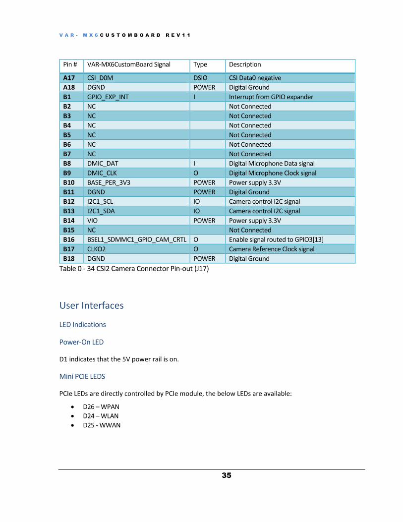
V A R - M X 6 C U S T O M B O A R D R E V 1 1
35
Pin # VAR-MX6CustomBoard Signal Type Description
A17 CSI_D0M DSIO CSI Data0 negative
A18 DGND POWER Digital Ground
B1 GPIO_EXP_INT I Interrupt from GPIO expander
B2 NC Not Connected
B3 NC Not Connected
B4 NC Not Connected
B5 NC Not Connected
B6 NC Not Connected
B7 NC Not Connected
B8 DMIC_DAT I Digital Microphone Data signal
B9 DMIC_CLK O Digital Microphone Clock signal
B10 BASE_PER_3V3 POWER Power supply 3.3V
B11 DGND POWER Digital Ground
B12 I2C1_SCL IO Camera control I2C signal
B13 I2C1_SDA IO Camera control I2C signal
B14 VIO POWER Power supply 3.3V
B15 NC Not Connected
B16 BSEL1_SDMMC1_GPIO_CAM_CRTL O Enable signal routed to GPIO3[13]
B17 CLKO2 O Camera Reference Clock signal
B18 DGND POWER Digital Ground
Table 0 - 34 CSI2 Camera Connector Pin-out (J17)
User Interfaces
LED Indications
Power-On LED
D1 indicates that the 5V power rail is on.
Mini PCIE LEDS
PCIe LEDs are directly controlled by PCIe module, the below LEDs are available:
• D26 – WPAN
• D24 – WLAN
• D25 - WWAN

V A R - M X 6 C U S T O M B O A R D R E V 1 1
36
Control Buttons
Power-On (SW1)
Power-On Switch, enable VAR-MX6Customboard main power
Reset Button (SW4)
System Hardware-reset
User Button (SW2)
Software controllable button
Boot Select (SW3)
The boot select switch sets the VAR-SOM-MX6 boot source and sequence. Refer to the VAR-SOM-MX6 module data sheet for a detailed description.
Position Logic Level Boot Source
Released ‘1’ On-SOM NAND flash
Pressed ‘0’ External (SD/MMC)
Table 0 - 35 Boot Select Switch Modes
Power Input (J18/J19)
The VAR-MX6CustomBoard is powered by a 7.5 V to 12 V DC power supply, using one of the connectors below (assembly option).
DC-in Jack (J19)
The DC-in power jack is compatible with a standard 2.5 mm / 5.5 mm power plug.
Terminal Block (J18)
A Terminal Block can be assembled if a DC jack is not required
Pin # Signal
1 PWR_IN1 2 PWR_IN2
Table 0 - 36 Terminal Block Connector Pin-out (J19)

V A R - M X 6 C U S T O M B O A R D R E V 1 1
37
RTC Backup Battery (JBT1)
The VAR-MX6CustomBoard features a CR1225 battery holder powering the VAR-MX6Customboard's DS1337 RTC.

V A R - M X 6 C U S T O M B O A R D R E V 1 1
38
Absolute Maximum Electrical Specifications
Min Max
Main Power Supply DC-IN -0.3 V 23 V
External Interfaces Unless otherwise specified, refer to the VAR-SOM-MX6 data sheet
Table 0 - 37 Absolute Maximum Electrical Specifications
Operational Electrical Specifications
Min Max
Main Power supply, DC-IN 7.5V 12V
External Interfaces Unless otherwise specified refer to VAR-SOM-MX6 data sheet
Table 0 - 38 Operational Electrical Specifications

V A R - M X 6 C U S T O M B O A R D R E V 1 1
39
Legal Notice Variscite Ltd. (“Variscite”) products and services are sold subject to Variscite terms and conditions of sale, delivery and payment supplied at the time of order acknowledgement.
Variscite warrants performance of its products to the specifications in effect at the date of shipment. Variscite reserves the right to make changes to its products and specifications or to discontinue any product or service without notice. Customers should therefore obtain the latest version of relevant product information from Variscite to verify that their reference is current.
Testing and other quality control techniques are utilized to the extent that Variscite deems necessary to support its warranty.
Specific testing of all parameters of each device is not necessarily performed unless required by law or regulation.
In order to minimize risks associated with customer applications, the customer must use adequate design and operating safeguards to minimize inherent or procedural hazards. Variscite is not liable for applications assistance or customer product design. The customer is solely responsible for its selection and use of Variscite products. Variscite is not liable for such selection or use or for use of any circuitry other than circuitry entirely embodied in a Variscite product.
Variscite products are not intended for use in life support systems, appliances, nuclear systems or systems where malfunction can reasonably be expected to result in personal injury, death or severe property or environmental damage. Any use of products by the customer for such purposes is at the customer’s own risk.
Variscite does not grant any license (express or implied) under any patent right, copyright, mask work right or other intellectual property right of Variscite covering or relating to any combination, machine, or process in which its products or services might be or are used. Any provision or publication of any third party’s products or services does not constitute Variscite’s approval, license, warranty or endorsement thereof. Any third party trademarks contained in this document belong to the respective third party owner.
Reproduction of information from Variscite datasheets is permissible only if reproduction is without alteration and is accompanied by all associated copyright, proprietary and other notices (including this notice) and conditions. Variscite is not liable for any un-authorized alteration of such information or for any reliance placed thereon.
Any representations made, warranties given, and/or liabilities accepted by any person which differ from those contained in this datasheet or in Variscite’s standard terms and conditions of sale, delivery and payment are made, given and/or accepted at that person’s own risk. Variscite is not liable for any such representations, warranties or liabilities or for any reliance placed thereon by any person.
2 Warranty Terms Variscite guarantees hardware products against defects in workmanship and material for a period of one (1) year from the date of shipment. Your sole remedy and Variscite’s sole liability shall be for Variscite, at its sole discretion, to either repair or replace the defective hardware product at no charge or to refund the purchase price. Shipment costs in both directions are the responsibility of the customer. This warranty is void if the hardware product has been altered or damaged by accident, misuse or abuse.

V A R - M X 6 C U S T O M B O A R D R E V 1 1
40
Disclaimer of Warranty
THIS WARRANTY IS MADE IN LIEU OF ANY OTHER WARRANTY, WHETHER EXPRESSED, OR IMPLIED, OF MERCHANTABILITY, FITNESS FOR A SPECIFIC PURPOSE, NON-INFRINGEMENT OR THEIR EQUIVALENTS UNDER THE LAWS OF ANY JURISDICTION, EXCEPT THE WARRANTY EXPRESSLY STATED HEREIN. THE REMEDIES SET FORTH HEREIN SHALL BE THE SOLE AND EXCLUSIVE REMEDIES OF ANY PURCHASER WITH RESPECT TO ANY DEFECTIVE PRODUCT.
Limitation on Liability
UNDER NO CIRCUMSTANCES SHALL VARISCITE BE LIABLE FOR ANY LOSS, DAMAGE OR EXPENSE SUFFERED OR INCURRED WITH RESPECT TO ANY DEFECTIVE PRODUCT. IN NO EVENT SHALL VARISCITE BE LIABLE FOR ANY INCIDENTAL OR CONSEQUENTIAL DAMAGES THAT YOU MAY SUFFER DIRECTLY OR INDIRECTLY FROM USE OF ANY PRODUCT.

V A R - M X 6 C U S T O M B O A R D R E V 1 1
41
3 Contact Information
Headquarters: Variscite Ltd. Variscite Ltd. 4, Hamelacha Street Lod 71520 Israel
Tel: +972 (9) 9562910 Fax: +972 (9) 9589477
Sales: [email protected]
Technical Support: [email protected]
Corporate Website: www.variscite.com