Embed Size (px)
Citation preview

VCT 49xyIEco CTV Designwith DSP Technology
Edition Dec. 20, 20046251-573-4-1AK
APPLICATION NOTE KITS/BOARDS
MICRONAS
MICRONAS

VCT 49xyI APPLICATION NOTE KITS/BOARDS
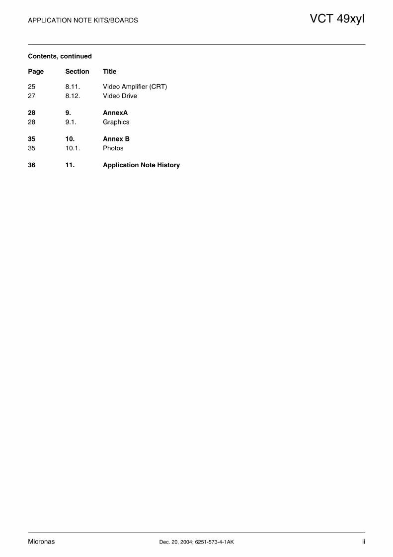
Contents
Page Section Title
2 1. Introduction to VCTI – DSP IC from Micronas2 1.1. Introduction to Priyanka 2 Chassis
3 2. Key Words
3 3. Priyanka 2 Chassis Specification3 3.1. Main Features3 3.2. Mechanical Aspects of the Chassis3 3.3. Front Panel Controls4 3.4. Key Components4 3.5. Power Supply4 3.6. Deflection/Picture Tube
4 4. PCB Architecture
5 5. Function Block Description5 5.1. Tuner5 5.2. VIF5 5.3. Source Selection5 5.4. Multistandard Sound Processing7 5.5. Video and Multistandard Chroma Processing7 5.6. Video Output7 5.7. Horizontal Output7 5.8. Vertical Output7 5.9. Audio Output7 5.10. Power Supply8 5.11. Local Key Pads, IR and Control8 5.12. VCTI DSP8 5.13. Pin Configuration and Short Description
12 6. Performance Details
12 7. Field Report12 7.1. Sound Crackling in some Channels13 7.2. ESD Hints13 7.3. Video Issues
14 8. Bill of Material Parts List14 8.1. Tuner/IF14 8.2. Front Panel15 8.3. Control and Memory16 8.4. VCTI18 8.5. Vertical Stage19 8.6. Horizontal Stage21 8.7. Audio Power Amplifier Part List21 8.8. External AV Input/Output Parts23 8.9. Regulators23 8.10. Power Supply Stage (Sanken)
i Dec. 20, 2004; 6251-573-4-1AK Micronas
Contents, continued
Page Section Title
APPLICATION NOTE KITS/BOARDS VCT 49xyI
25 8.11. Video Amplifier (CRT)27 8.12. Video Drive
28 9. AnnexA28 9.1. Graphics
35 10. Annex B35 10.1. Photos
36 11. Application Note History
Micronas Dec. 20, 2004; 6251-573-4-1AK ii

VCT 49xyI APPLICATION NOTE KITS/BOARDS
Eco CTV Design with DSP Technology
1. Introduction to VCTI – DSP IC from Micronas
In the television industry, Micronas is well known assupplier of DSP ICS for high-end television and multi-media products for the last few decades. The maindevelopment labs are in Germany at Freiburg andMunich. Micronas is well-known for the digital signalprocessing capabilities for audio and video relatedapplications and they are the market leaders for PIP,double scan, text and NICAM decoders, and digitaltelevision.
Expanding its comprehensive TV system solutionsoffering, Micronas has launched the new VCT 49xyIfamily platform, a complex, yet flexible single-chip TVsolution integrating all IF, audio, video, and control pro-cessing functions into one package. Uniquely sup-porting every TV standard worldwide, the software-and pin-compatible chips can be used in both low-cost mono and high-end TV sets featuring large screenreal flat 16:9 and surround sound.
With one board layout and software design, systemmanufacturers are able to target a range of differentmarkets, reducing development time and cost, as wellas the number of components. Especially for theseproducts, Micronas developed a new package for cus-tomers to lower production costs. Almost all non stan-dard field conditions can be managed with the rich setof VCTI registers. This means, for the TV manufactur-ers, more time is available for quality improvementsand improved market share.
The VCT 49xyI covers all TV Audio standards world-wide, from mono, BTSC-SAP,A2 system, and up toNICAM. It contains the complete audio base-band pro-cessing for up to three loudspeaker applications. Apartfrom basic audio features, the VCT 49xyI includesadvanced sound processing algorithms like: MicronasBASS, Micronas VOICE, Micronas AROUND, SRS,SRS WOW, BBE digital and Virtual Dolby Surround(VDS).
In addition to TV audio, the VCT 49xyI chips can alsoprocess FM radio programs including the radio dataservices RDS and RBDS (USA) without the need forany additional components. The CRT is a perfectmedium to display the information transmitted viathese data services.
The VCT 49xyI family covers all video standardsworldwide - automatic multistandard color demodula-tor. Due to the integrated rich set of video features, e.g.comb filter, horizontal scalar, picture improvementsand the advanced deflection unit, the chip can be usedfrom low-end up to high-end (large screen real flat16:9) TV sets.
The embedded TV controller supports all kinds of TVdata services, including WST, VPS, PDC, CC, V-chipand WSS. The advanced OSD (on-screen display)engine is used to generate sophisticated user menus.It is even possible to compress moving images andtext in order to display images and teletext or userinformation side by side - an impressive feature for16:9 screens. For the cost-sensitive single-scan TV market, Micro-nas offers another special advantage. The VCT 49xyIchips are available in a brand new, cost-effective 88 pinPSSDIP package. The PSSDIP has been specificallydeveloped following customer requests. It is similar toa DIP, but the pins are arranged to increase pin count,keeping package dimensions small. In addition toPSSDIP, the VCT 49xyI is available in standard 144-pin Quat Flat Package (QFP). With this package, anexternal SRAM can be connected to store up to 1,000teletext pages and to support EPG services.
1.1. Introduction to Priyanka 2 Chassis
The Priyanka chassis meets the needs of the vastmarket segment of low cost but good performance TVreceivers with standard features. Three aspectsachieve the low cost target. The cost optimized scal-able architecture of VCTI, low cost–low componentcount peripherals around VCTI and careful selection oflow cost power supply, deflection, audio and videooutput stages. The chassis is designed in a standardPCB size that is very small and yet can be mounted inmost of the TV cabinets. In production, twin PCBs canbe stuffed together and wave soldered thus improvingproductivity.
A detachable power supply (based on Sanken supplycontroller) module and keyboard is introduced in thesame small dimension of the chassis to meet applica-tions where cabinets are to be reduced and yet thecost has to be kept low. This also helps to improve ser-viceability needs of the developing nations with mini-mum tools.
Connectors are reduced to minimum without scarifyingflexibility. For example, since the video amplifier,power supply, and keyboard are breakaway part of themotherboard, direct wiring is possible without need oftwo connectors. Unlike other brands of single chip TVICs that have no audio processing, comb filter, or ste-reo source selection and hence external ICs areneeded for such functions, no additional ICs or mod-ules are needed with VCTI present.
2 Dec. 20, 2004; 6251-573-4-1AK Micronas
APPLICATION NOTE KITS/BOARDS VCT 49xyI
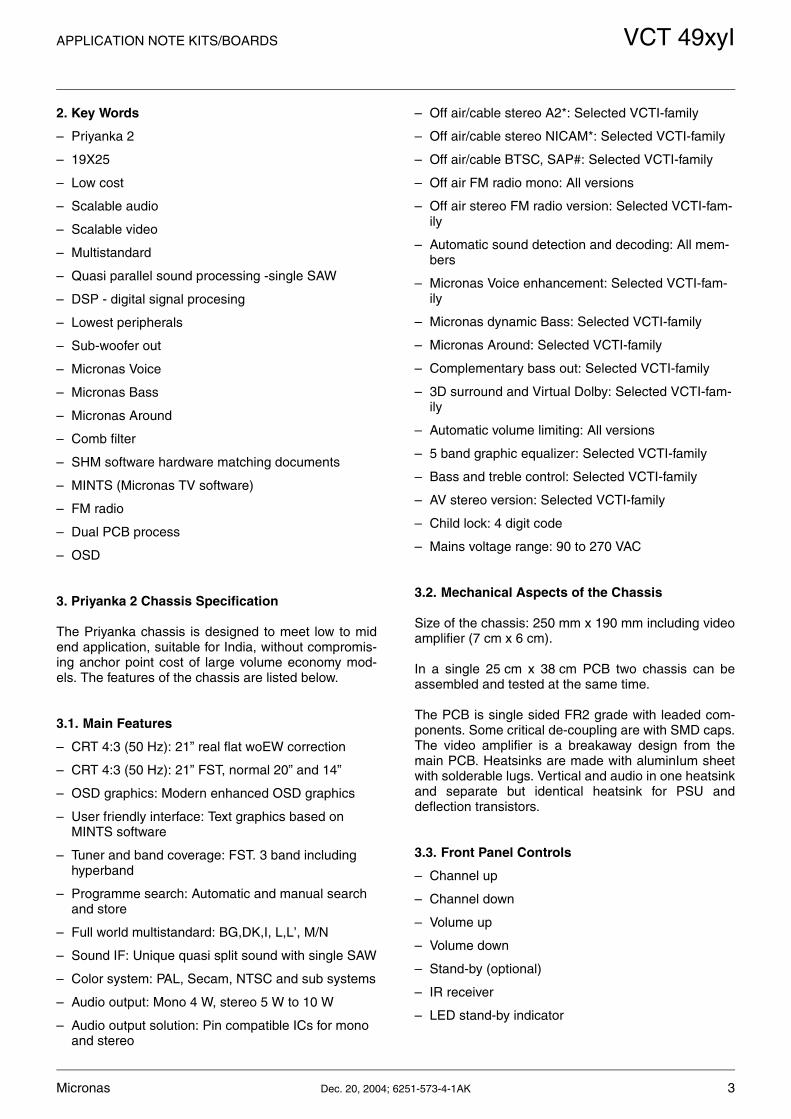
2. Key Words
– Priyanka 2
– 19X25
– Low cost
– Scalable audio
– Scalable video
– Multistandard
– Quasi parallel sound processing -single SAW
– DSP - digital signal procesing
– Lowest peripherals
– Sub-woofer out
– Micronas Voice
– Micronas Bass
– Micronas Around
– Comb filter
– SHM software hardware matching documents
– MINTS (Micronas TV software)
– FM radio
– Dual PCB process
– OSD
3. Priyanka 2 Chassis Specification
The Priyanka chassis is designed to meet low to midend application, suitable for India, without compromis-ing anchor point cost of large volume economy mod-els. The features of the chassis are listed below.
3.1. Main Features
– CRT 4:3 (50 Hz): 21” real flat woEW correction
– CRT 4:3 (50 Hz): 21” FST, normal 20” and 14”
– OSD graphics: Modern enhanced OSD graphics
– User friendly interface: Text graphics based on MINTS software
– Tuner and band coverage: FST. 3 band including hyperband
– Programme search: Automatic and manual search and store
– Full world multistandard: BG,DK,I, L,L’, M/N
– Sound IF: Unique quasi split sound with single SAW
– Color system: PAL, Secam, NTSC and sub systems
– Audio output: Mono 4 W, stereo 5 W to 10 W
– Audio output solution: Pin compatible ICs for mono and stereo
– Off air/cable stereo A2*: Selected VCTI-family
– Off air/cable stereo NICAM*: Selected VCTI-family
– Off air/cable BTSC, SAP#: Selected VCTI-family
– Off air FM radio mono: All versions
– Off air stereo FM radio version: Selected VCTI-fam-ily
– Automatic sound detection and decoding: All mem-bers
– Micronas Voice enhancement: Selected VCTI-fam-ily
– Micronas dynamic Bass: Selected VCTI-family
– Micronas Around: Selected VCTI-family
– Complementary bass out: Selected VCTI-family
– 3D surround and Virtual Dolby: Selected VCTI-fam-ily
– Automatic volume limiting: All versions
– 5 band graphic equalizer: Selected VCTI-family
– Bass and treble control: Selected VCTI-family
– AV stereo version: Selected VCTI-family
– Child lock: 4 digit code
– Mains voltage range: 90 to 270 VAC
3.2. Mechanical Aspects of the Chassis
Size of the chassis: 250 mm x 190 mm including videoamplifier (7 cm x 6 cm).
In a single 25 cm x 38 cm PCB two chassis can beassembled and tested at the same time.
The PCB is single sided FR2 grade with leaded com-ponents. Some critical de-coupling are with SMD caps.The video amplifier is a breakaway design from themain PCB. Heatsinks are made with aluminIum sheetwith solderable lugs. Vertical and audio in one heatsinkand separate but identical heatsink for PSU anddeflection transistors.
3.3. Front Panel Controls
– Channel up
– Channel down
– Volume up
– Volume down
– Stand-by (optional)
– IR receiver
– LED stand-by indicator
Micronas Dec. 20, 2004; 6251-573-4-1AK 3

VCT 49xyI APPLICATION NOTE KITS/BOARDS
3.4. Key Components
– Video_ Control_ TXT_ IF processor: VCT 49xyI (PSSDIP88-1)
– Audio amplifier (mono 4 W): AN7523 Matsushita
– Audio amplifier (stereo 5 W+5 W): AN7522 Mat-sushita
– Audio amplifier (stereo 10 W+10 W): AN17820
– Low voltage regulators: LM317 ST
– Vertical IC: TDA 8172 ST
– Horizontal transistor: BU508D ST
– SMPS power controller
– Frequency synthesis tuner: Philips UV1316
– SAW filter: Epcos X6966M
– Eeprom: ST
– Crystal 20.25: Vishay
– Fast recovery diodes (BA157): Vishay
– Bridge diodes: Vishay
– Wound components
– SMPS trafo: Utsavgiri
– Line output: Philips
– H-driver, line filter, Lin coil: Elcompo
3.5. Power Supply
Discrete self-oscillating power supply with large mainsvoltage range as needed in many countries where themains voltage fluctuation is large. The PSU can takeinputs from 90 V to 270 V without any visible perfor-mance degradation.
During switch on from cold, the stand-by power sup-plies, 3.3 V stand-by and 1.8 V stand-by will come firstpowering the VCTI start pins (on during stand-by).When H-deflection starts, the remaining small signalsupplies, namely the 5 V and 3.3 V, are derived fromthe aux DC from the secondary line transformer (auxsupply +12 V).
Nominal voltage 240 VMains Elco 450 VNominal power consumption 21” 70 WAutomatic stand-by, if no transmission for 6 minutes.
3.6. Deflection/Picture Tube
– Screen size from 14” to 25”
– Deflection circuit adaptation (vertical and horizontal) is needed due to yoke parameter variation
– Flyback transformer adaptation needed due to dif-ferent EHT requirements
4. PCB Architecture
The chassis architecture is shown in Fig. 4–1 below.
Fig. 4–1: Eco CTV Design with DSP Technology
Rear AV _In_Out
RF IN
VCT I
SMPS
Mains
Degaussing
H Defln
V.Defln
Speaker St or Mono
Subwoofer
LOT
Front AV cons
•5 V •3V3•3V3•1V8
+12 V ver -12 V ver 110 V
11 V8 V
•••
Fil, Grnd 180V
BU506D
Video Amp
SAWF
Supplies from SMPS+110V H-defln and for 32 V tuning+11 V Audio, H driver+ 8 V small signal DCfor 5 V 3.3 V 1.8 V
Supplies from LOT+ 180 V for video amp+/- 12 V for vertical EHT, VG2 and Focus
4 Dec. 20, 2004; 6251-573-4-1AK Micronas

APPLICATION NOTE KITS/BOARDS VCT 49xyI
5. Function Block Description
A short summary of different blocks relevant to thePriyanka chassis is presented here. For completedetails refer to VCTI data sheets. The chassis sup-ports the scalability of the VCTI family to some extent.However, due to limited scope of the chassis coveringthe Eco section of TV market, all versions of VCTI arenot usable. The following short descriptions are relatedto scope of Priyanka chassis alone. The capabilities ofVCTI far exceed the scope of the Priyanka chassis andkindly refer to detailed data sheets of VCTI and itsdiversity.
5.1. Tuner
The tuner used is the PLL tuner type Temic 6002PH5or Philips UV 1316. Although the I2C tuner address isthe same, there could be difference in the register datafor different tuners. The tuner supply voltage (5 V)comes from the main power supply unit (discreteSMPS) after the regulator LM317. The 33 V tuningsupply is derived from main supply 110 V from theSMPS (see PSU).
FM radio reception is possible, with reasonable perfor-mance and with appropriate VCTI. However, no spe-cial FM tuner is needed. A normal TV tuner that cantune the FM band (88 to 108 MHz) will do. The AGCfunction (pin 1 of the tuner) is controlled by VCTI(pin14). The tuner IF output is connected to universalSAW filter (8 MHz flat response) and the output of theSAW filter is connected to VCTI (pins16, 17) by shorttracks. After this, the signal processing is in digitaldomain. The tuner body ground is returned to supplyground by thick track for lightning protection.
Note: The AGC capacitor is only 10 nF.
5.2. VIF
This stage is different to conventional VIF stages. TheIF signals coming from the global SAW filter goesthrough an AGC stage before AD-conversion for digitalsignal processing. Complete QSS IF processing withan external single SAW filter (X6966M) is done by theVCTI for all global standards without need for switchingthe SAW filter, even in the case of multistandard TVapplications. (See details VCTI data sheets). Specificstandard dependant response and adaptation to trans-mitter or cable signal is possible in this section. TunerAGC take over point (TOP) adjustment and AFC func-tion are inside this section of IC. The output (CVBSand QSS SIF) is passed to further processing.
5.3. Source Selection
The chassis incorporates audio (2 channel stereo sig-nal) and video signal (CVBS) sockets on the mainboard. The source selection function is inside theVCTI. Recording output (monitor output) is availablefrom the rear of the main board from the Cinch con-nectors. ESD protection is achieved for the externalconnection by simple RC filters and spark gaps on thePCB tracks.
Crosstalk between sources is avoided by keeping trackisolation and short track lengths.
The selected signal source is internally processed andthe features of the audio and video processing arescalable according to the choice of VCTI. Sourceselection is done through I2C and so, no controllerports are needed for the source selection. The rear AVsource signals are fed to pins 12, 13 (audio L,R) and3§ (video). The front AV signals are fed to pins 10, 11(audio L, R) and 35 (video).
5.4. Multistandard Sound Processing
Different versions of VCTI (Eco and basic) can be usedon the chassis. In all versions, multistandard monodecoding is possible in automatic standard selectionmode or forced standard selection mode. See attachedtable for A2 system. For NICAM and BTSC standardsplease refer to VCTI, DSP data sheets.
The chassis can handle all known analog and NICAMTV sound transmission standards.
Thus, adaptations to different country standards arepossible. Either forced single standard (e.g. BG) orautomatic multistandard detection and processing ispossible with very little software overhead. The pro-cessed audio output is available for audio power ampli-fier (pins 4, 5). Audio output is also available at themonitor output (pins 6, 7).
For complete details of all audio features and descrip-tion, please refer to the software hardware matchingdocuments (SHM).
Micronas Dec. 20, 2004; 6251-573-4-1AK 5

VCT 49xyI APPLICATION NOTE KITS/BOARDS
Table 5–1: Key parameters of analog mono and two carrier standards
Characteristics Sound Carrier FM1 Sound Carrier FM2
TV sound standard B/G D/K M B/G D/K M
Carrier frequency in MHz 5.5 6.5 4.5 5.7421875 6.25781256.74218755.7421875
4.724212
Vision/sound power difference 13 dB 20 dB
Sound bandwidth 40 Hz to 15 kHz
Pre-emphasis 50 µs 75 µs 50 µs 74 µs
Frequency deviation (nom/max)
±27/±50 kHz ±17/±25 kHz ±27/±50 kHz ±17/±25 kHz
Transmission modes
Mono transmission Mono Mono
Stereo transmission (L+R)/2 (L+R)/2 R (L−R)/2
Dual sound transmission Language A Language B
Identification of transmission mode
Pilot carrier frequency 54.6875 kHz 55.0699 kHz
Max. deviation portion ±2.5 kHz
Type of modulation/modulation depth
AM/50%
Modulation frequency Mono: Non-modulatedStereo: 117.5 HzDual: 274.1 Hz
149.9 Hz276.0 Hz
Table 5–2: Key parameters of stereo FM radio transmission
Aural Carrier FM-Radio-MPX-Components
(L+R) Pilot (L−R) RDS/ARI
Carrier frequency (fp=19 kHz) 10.7 MHz Baseband fp 2 fp 3 fh
Sound bandwidth in kHz 0.05 − 15 0.05 − 15
Preemphasis:USAEurope
75 µs50 µs
75 µs50 µs
Max. deviation to aural carrier 75 kHz (100%) 90% 1) 10% 90% 1) 5%
1) Sum does not exceed 90% due to interleaving effects.
6 Dec. 20, 2004; 6251-573-4-1AK Micronas

APPLICATION NOTE KITS/BOARDS VCT 49xyI
5.5. Video and Multistandard Chroma Processing
External video CVBS (pins 33, 37) or internal videoCVBS from the tuner, after source selection, is passedto the multistandard chroma decoder. The color stan-dard can be identified and decoded automatically inauto mode or can be forced to a single standard.External (not on main PCB) YC or Y, Pb, Pr, or RGBcan also be processed. CVBS monitor output is avail-able on pin 40 through a buffer. A RGB output to CPTis available at the collector of the buffers (Q5, Q6, Q7).The details of the control functions of the color decoderis available in the SHM documents.
5.6. Video Output
A discrete video amplifier can be used due to the pos-sibility to independently adjust the cutoff and gainadjustments from the VCTI. This also helps to reducecost for Eco models.
However, if a reduction of RGB alignment in productionis needed, an auto cutoff feature can be enabled withappropriate video amplifier ICs like the TDA 6107.
5.7. Horizontal Output
The H-output from VCTI is accoupled to the bipolar H-driver BC337. Horizontal driver operates on a low volt-age (12 V) supply to reduce the cost of high voltagetransistor and elcos. The H-output is conventionalBU506D. The flyback capacitor is to be adjusted for dif-ferent H-yoke impedance. The H-output stage sup-ports only 90 deflections that needs no external geom-etry adjustments. The video amplifier supply (180 V)and vertical stage supplies (±13 V) is derived from theline deflection.
5.8. Vertical Output
The vertical output uses TDA 8172 of ST with dualsupply DC coupled yoke. This helps to implementblack switch off. Also the dual supply output stage pro-duces less vertical rattle.
All vertical parameters are adjustable from the DSP.Detection of vertical deflection failure is possible due toclamped vertical pulses applied to DSP (pin 59)V_protect. The set can be switched off automatically toavoid phosphor burnout mark. Vertical sync function isinside DSP with automatic sync to 50 Hz and 60 Hz.Note that the IC’s mounting tab is at –12 V and so, iso-lation is needed for mounting on the common heatsinkwith audio.
5.9. Audio Output
To meet different audio power requirement for differentmarket segments, a family of pin compatible audio out-put ICs from Matsushita is used.
– AN7523 up to 3 W (mono) at 11 V supply (16 Ohms)
– AN7522 up to 5 W + 5 W (stereo) at 11 V supply (8 Ohms)
– AN17820 up to 10 W+10 W (stereo) at 15 V audio supply (8 Ohms)
The first 9 pins of mono and stereo versions are ofcommon functions.
The audio amplifier can be put to stand-by mode bythe absence of DC voltage from aux supply from LOTat the stand-by pin of audio IC (pin5). Pin 9 is the mutepin and also the PWM volume control pin. If pin 9 isused as volume control the DSP audio output (pins 4,5) should be about 200 mV for nominal modulation of54%. If DSP volume is used, then the pin 9 of theaudio output should be held at 1.5 V to allow audiooutput to speakers. During switch on and switch offmute should be enabled to reduce PLOP sound at thespeakers.
5.10. Power Supply
The power supply is designed with the industry stan-dard Sanken controller that covers universal powersupply range (90 V to 270 V) operating in flybackmains isolated mode. The power supply can deliver upto 70 W RMS power to TV chassis.
The H-deflection supply is 112 V and audio supply is11 V or 15 V depending upon the power output. TheDC supply for the small signal is derived from anotheraux supply 8 V.
During stand-by the 5 V and some 3.3 V are switchedoff. LM317 regulators maintain part of 3.3 V and 1.8 V,which needs to be retained during stand-by. The inputfilters help to reduce line interference.
The mains elco is of higher voltage to take care of sup-ply voltage fluctuations on the higher side.
All the aux supplies are fitted with fuseable resistors toimprove short circuit and over current protection. Themains input is also fitted with a slow blow fuse a safetymeasure.
The on-off switch is mounted separately to improvecabinet flexibility.
Micronas Dec. 20, 2004; 6251-573-4-1AK 7

VCT 49xyI APPLICATION NOTE KITS/BOARDS
5.11. Local Key Pads, IR and Control
Usual 4-key local keypad is used for the channel andvolume changes. A fifth key can be used as stand-byswitch, where mains on-off switch is not mandatory.The IR receiver is supplied with 3.3 V and the receivedcode is input to pin 50. The LED is operated from theLED port (pin 53), which is on during stand-by and dimduring receiver on mode. The NVM stores standardsettings that are changed during operation of thereceiver by either user or by service personal tochange some service parameters. Few ports are avail-able for future expansion. The NVM is always writeprotected and anly write protected for writing into it,
controlled by the processor. This means that for even-tually CRT flashes, as well as pulses during switch offfrom mains, the NVM content is protected (pin 47 ofDSP).
5.12. VCTI DSP
The pinning details are given in the table below. To gethigh quality picture and sound with acceptable S/N theIC has dedicated supply and ground pins. The decou-pling ceramic capacitors are very close to IC pins. Thedecoupling chokes should have low self resistance(< 0.5 Ohms). The crystal frequency is 20.25 MHz.
5.13.Pin Configuration and Short Description
Pin No.
Pin Name Type Connection(If not used)
Short Description Priyanka Use
Application Function
1 GND SUPPLY OBL Ground platform Yes
2 VSUP8.0AU SUPPLY OBL Supply voltage analog audio 8.0 V
Yes 5 V used STD by OFF
3 VREFAU OBL Reference voltage, audio Yes
4 SPEAKERL OUT LV Analog loudspeaker output, left
Yes Volume con-trolled via MCU L- output
5 SPEAKERR OUT LV Analog loudspeaker output, right
Yes Volume con-trolled via MCU R-output
6 AOUT1L OUT LV Analog audio 1 output, left Yes Line out L
7 AOUT1R OUT LV Analog audio 1 output, right Yes Line out R
8 AIN3L/AOUT2L
IN/OUT LV Analog audio 3 input, left Analog audio 2 output, left
No Future use
9 AIN3R/AOUT2R
IN/OUT LV Analog audio 3 input, rightAnalog audio 2 output, right
No Future use
10 AIN2L IN GND Analog audio 2 input, left Yes Front audio in L
11 AIN2R IN GND Analog audio 2 input, right Yes Front audio in R
12 AIN1L IN GND Analog audio 1 input, left Yes Rear audio in 1L
13 AIN1R/SIF IN/OUT GND Analog audio 1 input, right Yes Rear audio in 1R
14 TAGC OUT LV Tuner AGC output Yes
15 VREFIF − OBL Reference voltage, IF ADC Yes
16 IFIN− IN VREFIF Differential IF input Yes
17 IFIN+ IN VREFIF Differential IF input Yes
8 Dec. 20, 2004; 6251-573-4-1AK Micronas

APPLICATION NOTE KITS/BOARDS VCT 49xyI
18 RESETQ IN/OUT OBL Reset input/output Yes 1Uf
19 VSUP5.0FE SUPPLY OBL Ground analog IF front-end Sup 5 V C4
Yes Off during stand-by
20 VSUP5.0IF SUPPLY OBL Supply voltage analog IF front-end, 5.0 V
Yes Off during stand-by
21 VSUP3.3DIG SUPPLY OBL Supply voltage digital core 3.3 V (main and stand-by supply)
Yes Off during stand-by
22 GND SUPPLY OBL Ground platform Yes
23 GND SUPPLY OBL Ground platform Yes
24 VSUP1.8DIG SUPPLY OBL Supply voltage digital core, 1.8 V (main and stand-by supply)
Yes On during stand-by
25 XTAL1 IN OBL analog crystal input Yes
26 XTAL2 OUT OBL Analog crystal output Yes
27 P22 IN/OUT LV Port 2, bit 2 input/output No
28 P23 IN/OUT LV Port 2, bit 3 input/output No
29 VIN11 IN GND Analog Video 11 input No
30 VIN10 IN GND Analog video 10 input No
31 VIN9 IN GND analog video 9 input No
32 VIN8 IN GND Analog video 8 input No
33 VIN7 IN GND Analog video 7 input Yes Front video in
34 VIN6 IN GND Analog video 6 input No
35 VIN5 IN GND Analog video 5 input Yes Rear video in 1
36 VIN4 IN GND Analog video 4 input No
37 VIN3 IN GND Analog video 3 input No
38 VIN2 IN GND Analog video 2 input No
39 VIN1 IN GND Analog video 1 input No
40 VOUT1 OUT LV Analog video 1 output Yes Video signal out-put
41 VOUT2 OUT LV Analog video 2 output No
42 VOUT3 OUT LV Analog video 3 output No
43 VSUP1.8FE SUPPLY OBL Supply voltage analog video front-end, 1.8 V
Yes On during stand-by
44 GND SUPPLY OBL Ground platform Yes
Pin No.
Pin Name Type Connection(If not used)
Short Description Priyanka Use
Application Function
Micronas Dec. 20, 2004; 6251-573-4-1AK 9

VCT 49xyI APPLICATION NOTE KITS/BOARDS
45 GND SUPPLY OBL Ground platform Yes
46 VSUP3.3FE SUPPLY OBL Supply voltage analog video front-end, 3.3 V
Yes On during stand-by
47 P10 IN/OUT LV Port 1, bit 0 input/output Yes Write protect
48 P11 IN/OUT LV Port 1, bit 1 input/output Yes Service modeExt
49 P12 IN/OUT LV Port 1, bit 2 input/output Yes Stand-by control
50 P13 IN/OUT LV Port 1, bit 3 input/output Yes IR input
51 P14 IN/OUT LV Port 1, bit 4 input/output Yes Keyboard
52 P15 IN/OUT LV Port 1, bit 5 input/output No
53 P16 IN/OUT LV Port 1, bit 6 input/output Yes LED port
54 P17 IN/OUT LV Port 1, bit 7 input(output Yes Keyboard
55 P20 IN/OUT LV Port 2, bit 0 input(output No
56 P21 IN/OUT LV Port 2, bit 1 input/output No
57 SCL IN/OUT OBL I2C Bus clock input/output Yes I2C Clk
58 SDA IN/OUT OBL I2C Bus data input/output Yes I2C SDA
59 VPROT IN GND Vertical Protection input Yes
60 HOUT OUT LV Horizontal drive output Yes
61 HFLB IN HOUT Horizontal flyback input Yes Clamped to Z3v3
62 SAFETY IN GND Safety input Yes
63 GNDDAC SUPPLY OBL Ground video DACs Yes
64 VSUP3.3DAC SUPPLY OBL Supply voltage video DACs, 3.3 V
Yes Off during stand-by
65 VSUP3.3IO SUPPLY OBL Supply voltage I/O ports, 3.3 V
Yes On during stand-by
66 GND SUPPLY OBL Ground platform Yes
67 GND SUPPLY OBL Ground platform Yes
68 VSUP3.3BE SUPPLY OBL Supply voltage analog video back-end, 3.3 V
Yes Off during stand-by
69 XREF OBL Reference current for RGB DACs
Yes
70 VRD OBL Reference voltage for RGB DACs
Yes
71 BOUT OUT VSUP5.0BE Analog blue output Yes Blue out
72 GOUT OUT VSUP5.0BE Analog green output Yes Green out
Pin No.
Pin Name Type Connection(If not used)
Short Description Priyanka Use
Application Function
10 Dec. 20, 2004; 6251-573-4-1AK Micronas

APPLICATION NOTE KITS/BOARDS VCT 49xyI
73 ROUT OUT VSUP5.0BE Analog red output Yes Red out
74 SVMOUT OUT VSUP5.0BE Scan velocity modulation output
No
75 BIN IN GND Analog blue input, back-end No
76 GIN IN GND Analog green input, bakc-end
No
77 RIN IN GND Analog red input, back-end No
78 FBIN IN GND Fast blakn input, back-end Yes 1k2 to Gnd
79 GNDM IN GND Reference ground for sense ADC
Yes
80 SENSE IN GND Sense ADC input Yes To be changed
81 RSW1 OUT LV Range switch 1 output Yes To be changed
82 RSW2 OUT LV Range switch 2 output Yes To be changed
83 EW OUT LV Vertical parabola output Yes
84 VERT− OUT LV Differential vertical saw-tooth output
Yes
85 VERT+ OUT LV Differential vertical saw-tooth output
Yes
86 TEST IN GND/SWOUT
Test input, reserved for Test Yes Sub-woofer out
87 VSUP5.0BE SUPPLY OBL Supply voltage analog video back-end, 5.0 V
Yes Off during stand-by
88 GND SUPPLY OBL Ground platform Yes
NC= Not connectedLV= If not used, leave vacantOBL= Obligatory; connect as described in circuit diagramIN= Input pinOUT= Output pinSUPPLY= Supply pin
Pin No.
Pin Name Type Connection(If not used)
Short Description Priyanka Use
Application Function
Micronas Dec. 20, 2004; 6251-573-4-1AK 11

VCT 49xyI APPLICATION NOTE KITS/BOARDS
6. Performance Details
A short summary of few critical measurements andtypical performance are given in Fig. 6–1
7. Field Report
Although most of the manufacturers have a lot of expe-rience to solve the field complaints, there is alwayssomething typical to key components in a new designand a summary of some problems and solutions aregiven. However, please contact our tech staff in caseyou need more latest updates.
7.1. Sound Crackling in some Channels
Picture is normal but sound is crackling. Most oftendue to the following reasons:
– Sound carrier level lower than normal.
– SIF centre frequency far from normal (say 150 kHz)
– Above + over modulation
Cause of crackling is when carrier level is too low forautomatic detection or off set and deviation is largeand so the sound demodulation fails on peaks ofsound. It is possible to switch on the over modulationbit to solve most of over modulation problems. Severecentre freq shift (>200 kHz) needs an algorithm todetect and correct the centre freq shift. It is better tomanually change the freq of DCO and store in NVM.
– Sound crackling due to week wanted channel (N) and strong adjacent channel (N+1) in VHF bands
The adjacent channel video gets passed along withthe wanted SIF to the audio detector. In case that theadjacent channel video is higher than the wantedsound carrier and appears as SIF, then the audiodecoder section detects this frequency as unknownstandard. In that case, the audio may be muted.
This can be solved by forced mode to wanted stan-dard.
– Strong chroma identified as M-system in multistan-dard set with week sound carrier
Table 6–1: Summary of measurements and typical performance
1 Video S/N for 60 dBuV of antenna signal
> 40 dB
2 Video S/N at Cinch out > 40 dB
3 Minimum antenna signal for tuning lock
32 dBuV
4 Colour loss at (RF signal) PAL & NTSC
< 27 dBuV
5 Signal handling capacity ( RF) > 100 dBuV
6 Colour catching with sub car-rier freq change
> ±300 Hz
7 Colour loss at subcarrier attenuation
> 29 dB
8 Sync compression range for H- and V-sync
10% of nomi-nal sync
9 H-sync catching > 4%
10 V-sync catching > 5%
11 THD at 1 W output < 1%
12 Audio frequency response low < 60 Hz
13 Audio frequency response high
> 12 kHz < 15 kHz
14 Audio S/N at 1 W output @1 kHz (black pic)
> 50 dB
15 Audio S/N at Cinch output @1 kHz (black pic)
> 50 dB
16 Audio S/N ratio with different pattern
> 40 dB
17 Audio noise limited sensitivity (46 dB S/N)
< 35 dBuV
18 Cross talk attenuation between L&R at all inputs
> 40 dB
19 Audio input for rated audio output
250 mV rms
20 Maximum input for rated audio input ( 5 V sup)
1 V rms
21 Audio output before limiting at Cinch out
1 V rms
22 Time for correct Sound and picture setting
< 12 secs
23 Bass Boost/ cut ±10 dB
24 Treble boost/cut ±10 dB
25 Equaliser variations (100 Hz,300 Hz, 1 k,3 k,10 k)
±10 dB
Table 6–1: Summary of measurements and typical performance, continued
12 Dec. 20, 2004; 6251-573-4-1AK Micronas

APPLICATION NOTE KITS/BOARDS VCT 49xyI
In auto-detect mode in a multistandard set if thechroma is stronger than the wanted SIF, then the audiodecoder is set to decode 4.5 MHz audio, which is notpresent.
To solve this, M-standard can be excluded in searchmode or manually force the standard to wanted one.
– Audible sound rattle (vertical flyback in audio) when ambient noise is very low (night listening)
If the volume control is in DSP and audio amplifier gainis high, some critical customers can complain aboutvertical rattle in night listening. It is better to use PWMvolume control at the power amplifier, which reducesthe power amplifier gain under low volume conditionsand significantly improves the S/N.
7.2. ESD Hints
– IC fails to receive IR commands
In case the IR receiver is located far away from thechassis and routed to the chassis by wires, it is possi-ble that the wires pickup ESD from EHT and the IRinput can fail. It is better to clamp the IR input line withadditional external diode and a small cap (<100 p) toground.
– Latch-up during ESD tests on I/Os
If the chassis goes to latch up mode during ESD tests,the use of Zener clamping diodes, as last resort, is rec-ommended, if simple RC decoupling fails. It is advis-able to build small Spark gaps (><) near the AV inputsof 0.5 mm space to release some energy.
7.3. Video Issues
– Sync loss in some channels tbd
– Good signal but no colour tbd
– Switch off spot tbd
Micronas Dec. 20, 2004; 6251-573-4-1AK 13

VCT 49xyI APPLICATION NOTE KITS/BOARDS
8. Bill of Material Parts List
8.1. Tuner/IF
8.2. Front Panel
Table 8–1: Tuner/IF
Sr No Component Type Value Rating Location Qty Pitch
1 CerCo CL2 Disc y5V 10 nF 50 V C1 1 5 mm
2 Elco CAN11 1 µF 50 V C2 1 5 mm
3 Elco CAN11 100 µF 10 V C3 1 5 mm
4 CerCo CL2 Disc y5V 100 nF − C5 1 5 mm
5 CerCo CL2 Disc y5V 10 nF 50 V C6 1 5 mm
6 CerCo CL2 Disc y5V 10 nF 50 V C7 1 5 mm
7 Zener 400 mW BZX4C33 − D1 1 7.5 mm
8 SAW filter Global filter X6966M 38.9 IF F1 1 −
9 Fuseable NFR 1 Ω 0.25 W R0 1 7.5 mm
10 Resistor Sfr 25H 22 k 0.5 W R1 1 12.5 mm
11 Resistor 16S 6.8 k − R2 1 7.5 mm
12 Resistor 16S 6.8 k − R3 1 10 mm
13 Tuner Philips UV1316 − − 1 −
Total 13
Table 8–2: Front panel
Sr No Component Type Value Rating Location Qty Pitch
1 Elco can11 10 µF 10 V C202 1 5 mm
2 CerCo CL1 Disc 100 pF 50 V C203 1 5 mm
3 LED Red 5 mm − D201 1 2.5 mm
4 Resistor 16S 470 Ω − R200 1 7.5 mm
5 Resistor 16S 2.7 k − R202 1 7.5 mm
6 Resistor 16S 3.3 k − R203 1 7.5 mm
7 Resistor 16S 6.8 k − R204 1 7.5 mm
8 Resistor 16S 15 k − R205 1 7.5 mm
9 Resistor 16S 2.2 k − R206 1 7.5 mm
10 Resistor 16S 2.2 k − R207 1 7.5 mm
11 Resistor 16S 100 Ω − R209 1 7.5 mm
14 Dec. 20, 2004; 6251-573-4-1AK Micronas

APPLICATION NOTE KITS/BOARDS VCT 49xyI
8.3. Control and Memory
12 Resistor 16S 15 k − R210 1 7.5 mm
13 IR receiver TSOP1836SS3V-M
IR 3.3 V IC201 1 7.5 mm
14 Keypad P + SW − sw201 1 7.5 mm
15 Keypad P − SW − sw202 1 7.5 mm
16 Keypad Vol + SW − sw203 1 7.5 mm
17 Keypad Vol − SW − sw204 1 7.5 mm
18 Keypad Menu SW − sw205 1 7.5 mm
Total 18
Table 8–2: Front panel, continued
Sr No Component Type Value Rating Location Qty Pitch
Table 8–3: Control and memory
Sr No Component Type Value Rating Location Qty Pitch
1 Resistor 16S 100 Ω − R251 1 7.5 mm
2 Resistor 16S 100 Ω − R252 1 7.5 mm
3 Resistor 16S 2.2 k − R253 1 7.5 mm
4 Resistor 16S 10 k − R254 1 7.5 mm
5 Elco can11 100 µF 10 V C251 1 5 mm
6 CerCo CL2 y5V 100 nF 50 V C252 1 5 mm
7 NVM − ST24C − IC251 1 −
8 Connector 5 pin − 2.5 mmpitch
− SK201 1 2.5 mm pin
Total 8
Micronas Dec. 20, 2004; 6251-573-4-1AK 15

VCT 49xyI APPLICATION NOTE KITS/BOARDS
8.4. VCTI
Table 8–4: VCTI
Sr No Component Type Value Rating Location Qty Pitch
1 CerCo CL2 y5V 100 nF 50 V C300 1 5 mm
2 Elco can11 100 µF 10 V C301 1 5 mm
3 CerCo CL2 y5V 100 nF 50 V C302 1 5 mm
4 CerCo CL2 y5V 100 nF 50 V C303 1 5 mm
5 Elco can11 100 µF 10 v C304 1 5 mm
6 CerCo CL2 y5V 100 nF 50 V C305 1 5 mm
7 CerCo CL2 y5V 100 nF 50 V C306 1 5 mm
8 Elco can11 100 µF 10 v C307 1 5 mm
9 CerCo CL2 y5V 100 nF 50 V C308 1 5 mm
10 Elco can11 100 µF 10 v C309 1 5 mm
11 CerCo CL1 can11 22 pF 50 V C310 1 5 mm
12 CerCo CL2 y5V 100 nF 50 V C311 1 5 mm
13 CerCo CL2 y5V 100 nF 50 V C312 1 5 mm
14 Elco can11 100 µF 10 v C313 1 5 mm
15 CerCo CL1 can11 22 pF 50V C314 1 5 mm
16 Elco can11 100 µF 10v C315 1 5 mm
17 CerCo CL2 y5V 100 nF 50 V C316 1 5 mm
18 CerCo CL2 y5V 100 nF 50 V C317 1 5 mm
19 Elco can11 100 µF 10 V C318 1 5 mm
20 Elco can11 4.7 µF 10 V C319 1 5 mm
21 Cap FFC 220 nF − C320 1 5 mm
22 CerCo CL2 y5V 100 nF 50 V C321 1 5 mm
23 CerCo CL2 y5V 100 nF 50 V C322 1 5 mm
24 Elco can11 100 µF 10 v C323 1 5 mm
25 CerCo CL2 y5V 100 nF 50 V C324 1 5 mm
26 CerCo CL2 y5V 100 nF 50 V C325 1 5 mm
27 CerCo CL2 y5V 100 nF 50 V C326 1 5 mm
28 Elco can11 3.3 µF 10 V C327 1 5 mm
29 CerCo CL2 y5V 100 nF 50 V C328 1 5 mm
30 Elco can11 100 µF 10 V C329 1 5 mm
16 Dec. 20, 2004; 6251-573-4-1AK Micronas

APPLICATION NOTE KITS/BOARDS VCT 49xyI
31 Elco can11 100 µF 10 V C330 1 5 mm
32 CerCo CL2 y5V 100 nF 50 V C334 1 5 mm
33 CerCo CL2 y5V 100 nF 50 V C336 1 −
34 Elco can11 100 µF 10 V C337 1 5 mm
35 CerCo CL2 y5V 100 nF 50 V C340 1 −
36 CerCo CL2 y5V 100 nF 50 V C341 1 5 mm
37 CerCo CL2 y5V 10 n 50 V C342 1 5 mm
38 CerCo CL2 y5V 100 nF 50 V C343 1 5 mm
39 Elco can11 100 µF 10 V C331 1 5 mm
40 SS Diode − 1N4148 − D301 1 7.5 mm
41 Crystal − 20.25 MHZ − F301 1 −
42 Inductance Axial 10 µH − L301 1 10 mm
43 Inductance Axial 10 µH − L302 1 10 mm
44 Inductance Axial 10 µH − L303 1 10 mm
45 Inductance Axial 10 µH − L304 1 10 mm
46 Inductance Axial 10 µH − L305 1 10 mm
47 Inductance Axial 10 µH − L306 1 7.5 mm
48 Inductance Axial 10 µH − L307 1 7.5 mm
49 Inductance Axial 10 µH − L308 1 10 mm
50 Resistor 16S 100 Ω − R301 1 7.5 mm
51 Resistor 16S 1.2 k − R303 1 7.5 mm
52 Resistor 16S 100 Ω − R304 1 15 mm
53 Resistor 16S 1.2 k − R305 1 7.5 mm
54 Resistor 16S 100 Ω − R306 1 15 mm
55 Resistor 16S 1 k − R307 1 7.5 mm
56 Resistor 16S 22 k − R308 1 7.5 mm
57 Resistor 16S 1.2 k − R309 1 7.5 mm
58 Resistor 16S 270 Ω − R310 1 7.5 mm
59 Resistor 16S 3.3 k − R311 1 7.5 mm
60 Resistor 16S 1.2 k − R312 1 7.5 mm
61 Resistor 16S 4.7 k − R313 1 7.5 mm
Table 8–4: VCTI, continued
Sr No Component Type Value Rating Location Qty Pitch
Micronas Dec. 20, 2004; 6251-573-4-1AK 17

VCT 49xyI APPLICATION NOTE KITS/BOARDS
8.5. Vertical Stage
62 Resistor 16S 2.2 k − R314 1 7.5 mm
63 Resistor 16S 1.2 k − R315 1 7.5 mm
64 Resister 16S 10 k − R318 1 7.5 mm
65 IC GMBH VCT492x − IC 1 −
66 Connector − 3-pin − SK301 A 1 −
67 Connector − 3-pin − SK301 B 1 −
68 Connector − 5-pin − SK301 1 −
69 Connector − 2-pin − SK302 1 −
Total 69
Table 8–4: VCTI, continued
Sr No Component Type Value Rating Location Qty Pitch
Table 8–5: Vertical stage
Sr No Component Type Value Rating Location Qty Pitch
1 CerCo CL2 y5V 47 nF 25 V C401 1 5 mm
2 CerCo CL2 y5V 47 nF 25 V C402 1 5 mm
3 Elco can11 220 µF 25 V C403 1 5 mm
4 Elco can11 100 µF 16 V C404 1 5 mm
5 CerCo CL2 y5V 100 nF 50 V C405 1 5 mm
6 CerCo CL2 y5V 10 nF 50 V C406 1 5 mm
7 CerCo CL2 y5V 47 nF 50 V C407 1 5 mm
8 Elco can11 100 µF 16 V C408 1 5 mm
9 CAP FFC 22 µF 63 V C409 1 5 mm
10 CerCo CL2 y5V 100 nF 50 V C410 1 5 mm
11 CerCo CL1 y5V 100 pF 50 V C411 1 5 mm
12 CerCo CL1 y5V 100 pF 50 V C412 1 5 mm
13 Diode − IN4007 − D401 1 15 mm
14 SS Diode − 1N4148 − D402 1 7.5 mm
15 SS Diode − 1N4148 − D403 1 7.5 mm
16 Resistor 16S 6.8 k − R401 1 7.5 mm
17 Resistor 16S 6.8 k − R402 1 7.5 mm
18 Resistor 16S 47 k − R403 1 10 mm
18 Dec. 20, 2004; 6251-573-4-1AK Micronas

APPLICATION NOTE KITS/BOARDS VCT 49xyI
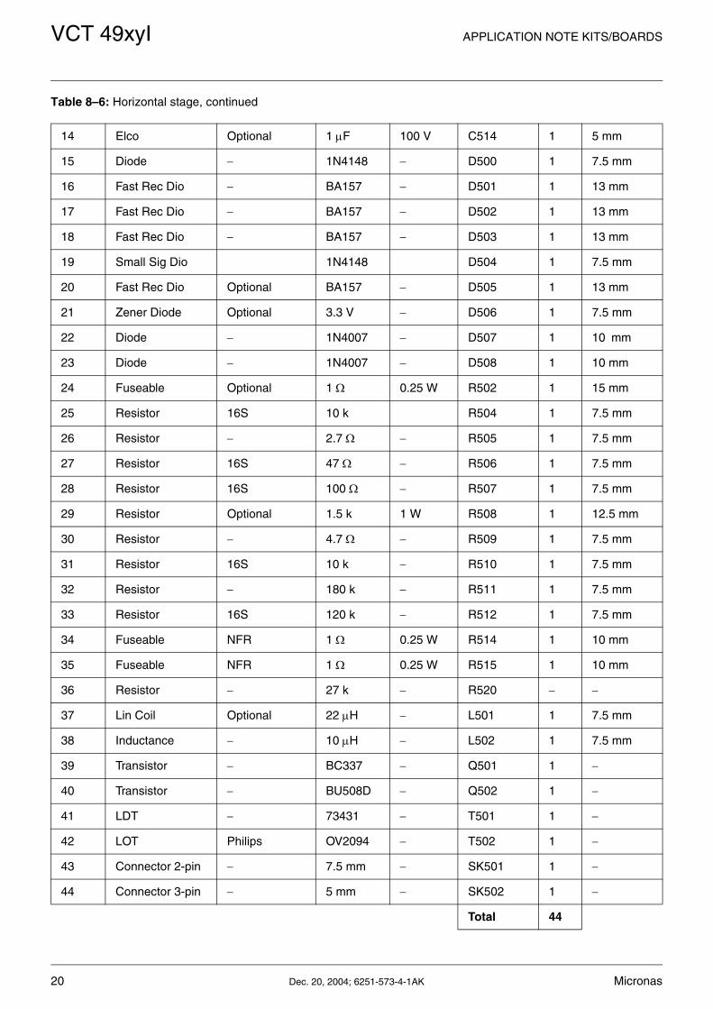
8.6. Horizontal Stage
19 Resistor 16S 33 k − R404 1 12.5 mm
20 Resistor 16S 47 k − R405 1 7.5 mm
21 Resistor 16S 4.7 k − R406 1 7.5 mm
22 Resistor 16S 100 k − R407 1 7.5 mm
23 Resistor 16S 6.8 k − R408 1 7.5 mm
24 Resistor 0.5 W 1.5 Ω − R409 1 12.5 mm
25 Resistor 16S 3.9 k − R410 1 7.5 mm
26 Resistor 16S 470 Ω − R411 1 7.5 mm
27 Resistor 16S 33 k − R412 1 10 mm
28 Resistor 0.5 W 2.2 Ω 0.5 W R413 1 12.5 mm
29 IC ST Micro Elec TDA 8172 − IC401 1 −
30 Inductance Axial 10 µH − L401 1 7.5 mm
31 Connector 2-pin − 2 pin 5 mm SK401 1 −
Total 31
Table 8–5: Vertical stage, continued
Sr No Component Type Value Rating Location Qty Pitch
Table 8–6: Horizontal stage
Sr No Component Type Value Rating Location Qty Pitch
1 Elco − 220 µF 25 V C501 1 5 mm
2 CerCo CL1 − 470 pF 50 V C502 1 5 mm
3 Film − 470 nF 250 V C503 1 23 mm
4 Elco − 47 µF 160 V C504 1 5 mm
5 Film − 8.2 nF 1500 V C505 1 23 mm
6 Elco − 1 µF 10 V C506 1 5 mm
7 HV CerCo − 330 pF 500 V C507 1 7.5 mm
8 HV CerCo − 330 pF 500 V C508 1 7.5 mm
9 HV Elco − 10 µF 250 V C509 1 5 mm
10 HV CerCo − 330 pf 500 V C510 1 7.5 mm
11 Elco − 220 µF 16 V C511 1 5 mm
12 Elco − 220 µF 16 V C512 1 5 mm
13 HV CerCo Optional 470 pF 2 kV C513 1 7.5 mm
Micronas Dec. 20, 2004; 6251-573-4-1AK 19
VCT 49xyI APPLICATION NOTE KITS/BOARDS
14 Elco Optional 1 µF 100 V C514 1 5 mm
15 Diode − 1N4148 − D500 1 7.5 mm
16 Fast Rec Dio − BA157 − D501 1 13 mm
17 Fast Rec Dio − BA157 − D502 1 13 mm
18 Fast Rec Dio − BA157 − D503 1 13 mm
19 Small Sig Dio 1N4148 D504 1 7.5 mm
20 Fast Rec Dio Optional BA157 − D505 1 13 mm
21 Zener Diode Optional 3.3 V − D506 1 7.5 mm
22 Diode − 1N4007 − D507 1 10 mm
23 Diode − 1N4007 − D508 1 10 mm
24 Fuseable Optional 1 Ω 0.25 W R502 1 15 mm
25 Resistor 16S 10 k R504 1 7.5 mm
26 Resistor − 2.7 Ω − R505 1 7.5 mm
27 Resistor 16S 47 Ω − R506 1 7.5 mm
28 Resistor 16S 100 Ω − R507 1 7.5 mm
29 Resistor Optional 1.5 k 1 W R508 1 12.5 mm
30 Resistor − 4.7 Ω − R509 1 7.5 mm
31 Resistor 16S 10 k − R510 1 7.5 mm
32 Resistor − 180 k − R511 1 7.5 mm
33 Resistor 16S 120 k − R512 1 7.5 mm
34 Fuseable NFR 1 Ω 0.25 W R514 1 10 mm
35 Fuseable NFR 1 Ω 0.25 W R515 1 10 mm
36 Resistor − 27 k − R520 − −
37 Lin Coil Optional 22 µH − L501 1 7.5 mm
38 Inductance − 10 µH − L502 1 7.5 mm
39 Transistor − BC337 − Q501 1 −
40 Transistor − BU508D − Q502 1 −
41 LDT − 73431 − T501 1 −
42 LOT Philips OV2094 − T502 1 −
43 Connector 2-pin − 7.5 mm − SK501 1 −
44 Connector 3-pin − 5 mm − SK502 1 −
Total 44
Table 8–6: Horizontal stage, continued
20 Dec. 20, 2004; 6251-573-4-1AK Micronas

APPLICATION NOTE KITS/BOARDS VCT 49xyI
8.7. Audio Power Amplifier Part List
8.8. External AV Input/Output Parts
Table 8–7: Audio power amplifier part list
Sr No Component Type Value Rating Location Qty Pitch
1 Elco Elco 10 µF 10 V C600 1 5 mm
2 Elco Elco 10 µF 10 V C601 1 5 mm
3 CerCo CL2 y5V 1 nF 50 V C602 1 5 mm
4 CerCo CL2 y5V 1 nF 50 V C603 1 5 mm
5 Elco Elco 10 µF 10 V C604 1 5 mm
6 Elco Elco 10 µF 10 V C605 1 5 mm
7 Elco Elco 100 µF 25 V C606 1 5 mm
8 CerCo CL2 y5V 100 nF 50 V C607 1 5 mm
9 Resistor 16S 2.2 k − R602 1 7.5 mm
10 Resistor 16S 3.3 k − R604 1 7.5 mm
11 Resistor 16S 10 k − R605 1 7.5 mm
12 Resistor 16S 22 k − R606 1 7.5 mm
13 Inductance − 10 µH − L601 1 10 mm
14 Connector 2pin − 2.5 mm − SK601 1 −
15 Connector 4pin − 2.5 mm − SK601 1 −
16 IC ST AN7522 − IC601 1 −
17 Speaker Philips 8 Ω − SP 601 1 −
18 Speaker Philips 8 Ω − SP602 1 −
Total 18
Table 8–8: External AV input/output
Sr No Component Type Value Rating Location Qty Pitch
1 Resistor 16S 220 Ω − R702 1 7.5 mm
2 Resistor 16S 1 k − R703 1 7.5 mm
3 Resistor 16S 75 Ω − R704 1 7.5 mm
4 Resistor 16S 75 Ω − R705 1 7.5 mm
5 Resistor 16S 100 Ω − R706 1 7.5 mm
6 Resistor 16S 180 k − R707 1 7.5 mm
7 Resistor 16S 100 Ω − R708 1 7.5 mm
Micronas Dec. 20, 2004; 6251-573-4-1AK 21
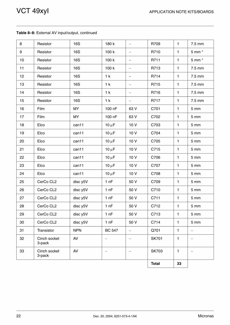
VCT 49xyI APPLICATION NOTE KITS/BOARDS
8 Resistor 16S 180 k − R709 1 7.5 mm
9 Resistor 16S 100 k − R710 1 5 mm *
10 Resistor 16S 100 k − R711 1 5 mm *
11 Resistor 16S 100 k − R713 1 7.5 mm
12 Resistor 16S 1 k − R714 1 7.5 mm
13 Resistor 16S 1 k − R715 1 7.5 mm
14 Resistor 16S 1 k − R716 1 7.5 mm
15 Resistor 16S 1 k − R717 1 7.5 mm
16 Film MY 100 nF 63 V C701 1 5 mm
17 Film MY 100 nF 63 V C702 1 5 mm
18 Elco can11 10 µF 10 V C703 1 5 mm
19 Elco can11 10 µF 10 V C704 1 5 mm
20 Elco can11 10 µF 10 V C705 1 5 mm
21 Elco can11 10 µF 10 V C715 1 5 mm
22 Elco can11 10 µF 10 V C706 1 5 mm
23 Elco can11 10 µF 10 V C707 1 5 mm
24 Elco can11 10 µF 10 V C708 1 5 mm
25 CerCo CL2 disc y5V 1 nF 50 V C709 1 5 mm
26 CerCo CL2 disc y5V 1 nF 50 V C710 1 5 mm
27 CerCo CL2 disc y5V 1 nF 50 V C711 1 5 mm
28 CerCo CL2 disc y5V 1 nF 50 V C712 1 5 mm
29 CerCo CL2 disc y5V 1 nF 50 V C713 1 5 mm
30 CerCo CL2 disc y5V 1 nF 50 V C714 1 5 mm
31 Transistor NPN BC 547 − Q701 1 −
32 Cinch socket 3-pack
AV − − SK701 1 −
33 Cinch socket3-pack
AV − − SK703 1 −
Total 33
Table 8–8: External AV input/output, continued
22 Dec. 20, 2004; 6251-573-4-1AK Micronas

APPLICATION NOTE KITS/BOARDS VCT 49xyI
8.9. Regulators
8.10.Power Supply Stage (Sanken)
Table 8–9: Regulators
Sr No Component Type Value Rating Location Qty Pitch
1 Resistor Carben 10 Ω 0.5 W R 805 1 15 mm
2 Resistor Carben 10 Ω 1 W R835 1 15 mm
3 Resistor Carben 330 Ω 0.125 W R810 1 7.5 mm
4 Resistor Carben 180 Ω 0.125 W R815 1 7.5 mm
5 Resistor Carben 330 Ω 0.125 W R816 1 7.5 mm
6 Resistor Carben 10 Ω 1 W R836 1 15 mm
7 Resistor Carben 47 Ω 1 W R837 1 7.5 mm
8 Resistor Carben 330 Ω 0.125 W R824 1 7.5 mm
9 Resistor Carben 560 Ω 0.125 W R825 1 7.5 mm
10 Resistor Carben 180 Ω 0.125 W R827 1 7.5 mm
11 Resistor Carben 330 Ω 0.125 W R828 1 7.5 mm
12 Zener Diode − 5.6 V 0.25 W D809 1 7.5 mm
13 Diode − 1N4148 − D820 1 7.5 mm
14 Transistor TO 220 B 2N5294 − Q806 1 −
15 Elco can11 100 µF 10 V C818 1 5 mm
16 Elco can11 100 µF 10 V C819 1 5 mm
17 Elco can11 10 µF 10 V C810 1 5 mm
18 Regulators TO 220 B LM317 − IC 801 1 −
19 Regulators TO 220 B LM317 − IC 801 1 −
20 Regulators TO 220 B LM317 − IC 801 1 −
Total 20
Table 8–10: Power supply stage (Sanken)
Sr No Component Type Value Rating Location Qty Pitch
1 Resistor 16S 100 k 0.25 W R851 1 14 mm
2 Resistor 16S 100 k 0.25 W R852 1 14 mm
3 Resistor − 0.18 Ω 2 W R853 1 18 mm
4 Resistor − 180 Ω 1 W R854 1 12.5 mm
5 Resistor 16S 150 k 0.25 W R856 1 20 mm
Micronas Dec. 20, 2004; 6251-573-4-1AK 23

VCT 49xyI APPLICATION NOTE KITS/BOARDS
6 Resistor − 1 k 0.25 W R857 1 10 mm
7 Resistor − 4.7 Ω 5 W R858 1 25 mm
8 Resistor 16S 1.5 k 0.25 W R859 1 10 mm
9 Resistor − 10 Ω 0.25 W R860 1 10 mm
10 Resistor − 6.8 Ω 0.25 W R861 1 12.5 mm
11 Resistor − 1 k 0.25 W R862 1 10 mm
12 Resistor − 1.2 k 0.25 W R863 1 10 mm
13 Resistor − 33 k 0.25 W R864 1 10 mm
14 Resistor − 47 k 0.25 W R865 1 10 mm
15 Resistor − 5.6 k 0.25 W R866 1 10 mm
16 Elco − 220 µF 400 V C851 1 10 mm
17 Disc − 100 nF 275 VAC C852 1 15 mm
18 Disc − 1.5 nF 1 KV C853 1 7.5 mm
19 Disc − 1 nF 50 V C854 1 7.5 mm
20 Disc - 100 nF 275VAC C855 1 15 mm
21 Elco - 4.7 µF 25 V C856 1 5 mm
22 Disc - 1.5 nF 50 V C857 1 7.5 mm
23 Elco - 47 µF 25 V C858 1 5 mm
24 Disc − 100 nF 50 V C859 1 7.5 mm
25 Disc − 1 nF 1.5 KV C860 1 7.5 mm
26 Elco − 1000 µF 25 V C867 1 7.5 mm
27 Disc - 1 nF 1.5 KV C861 1 7.5 mm
28 Disc - 2.2 nF 2 KV C862 1 7.5 mm
29 Disc − 1 nF 1 KV C863 1 7.5 mm
30 Disc − 1 nF 1 KV C865 1 7.5 mm
31 Disc − 1 nF 1 KV C866 1 7.5 mm
32 Elco − 1000 µF 16 V C868 1 5 mm
33 Elco − 1000 µF 25 V C869 1 5 mm
34 Disc − 47 nF 63 V C870 1 10 mm
35 Elco − 150 µF 160 V C871 1 7.5 mm
36 Diode − EU1Z D851 1 12.5 mm
Table 8–10: Power supply stage (Sanken), continued
Sr No Component Type Value Rating Location Qty Pitch
24 Dec. 20, 2004; 6251-573-4-1AK Micronas

APPLICATION NOTE KITS/BOARDS VCT 49xyI
8.11.Video Amplifier (CRT)
37 Diode − EU1Z − D852 1 12.5 mm
38 Diode − 1N4007 − D853 1 15 mm
39 Diode − 1N4007 − D854 1 40 mm
40 Diode − 1N4007 − D855 1 15 mm
41 Diode − 1N4007 − D856 1 15 mm
42 Diode − 6.2 V 10 mmZN D857 1 10 mm
43 Diode − EU1Z − D858 1 12.5 mm
44 Diode − RG2A − D859 1 15 mm
45 Diode − RG2Y − D860 1 15 mm
46 Diode − G12 − D861 1 5 mm
47 Diode − G12 − D862 1 5 mm
48 Fuse − 4A − F851 1 10 mm
49 Thermistor − PTC − P851 1 −
50 Mains Socket − 2-pin 7.5 P SK801 1 −
51 Deg Coil − 2-pin 5 mm SK852 1 5 mm
52 Output Socket − 5-pin 5 mm SK853 1 5 mm
53 Mains Filter − Filter − T851 1 −
54 SMPS Trans-former
− SMPS − T852 1 −
55 W6756 − STR 6756 − IC851 1 −
56 Optocoupler − − IC852 1 −
57 TL431 − IC Regula-tor
− IC853 1 −
58 F/B − − R855 1 −
Total 58
Table 8–10: Power supply stage (Sanken), continued
Sr No Component Type Value Rating Location Qty Pitch
Table 8–11: Video amplifier (CRT)
Sr No Component Type Value Rating Location Qty Pitch
1 Resistor 16S 1.5 k − R904 1 7.5 mm
2 Resistor LSR 37 1 k 1 W R905 1 15 mm
3 Resistor LSR 37 1 k 1 W R906 1 15 mm
Micronas Dec. 20, 2004; 6251-573-4-1AK 25

VCT 49xyI APPLICATION NOTE KITS/BOARDS
4 Resistor LSR 37 1 k 1 W R907 1 15 mm
5 Resistor 16S 4.7 k − R909 1 7.5 mm
6 Resistor 16S 1.2 k − R910 1 7.5 mm
7 Resistor 16S 1.2 k − R911 1 7.5 mm
8 Resistor 16S 1.2 k − R912 1 7.5 mm
9 Resistor 16S 1 k − R913 1 7.5 mm
10 Resistor 16S 1.5 k − R914 1 7.5 mm
11 Resistor 16S 180 k − R915 1 7.5 mm
12 Resistor 16S 5.6 k − R917 1 7.5 mm
13 Resistor 16S 220 Ω − R925 1 7.5 mm
14 HV Elco − 10 µF 250 V C900 1 5 mm
15 HV CerCo − 2.2 nF 2 kV C901 1 7.5 mm
16 HV CerCo − 2.2 nF 2 kV C902 1 7.5 mm
17 CerCo CL1 Optional 2.2 pF 50 V C903 1 5 mm
18 CerCo CL1 Optional 2.2 pF 50 V C904 1 5 mm
19 CerCo CL1 Optional 2.2 pF 50 V C905 1 5 mm
20 CerCo CL1 − 100 nF 250 V C906 1 7.5 mm
21 CerCo CL1 − 150 pF 50 V 907 1 5 mm
22 HV Elco − 4.7 µF 250 V C908 1 5 mm
23 Diode BA157 or BAV21 − D900 1 10 mm
24 Diode BA157 or BVA21 − D901 1 10 mm
25 Diode BA157 or BAV21 − D902 1 10 mm
26 Diode − IN 4007 − D903 1 10 mm
27 Transistor − BC557 − Q900 1 −
28 Transistor − BC547 − Q901 1 −
29 IC Philips TDA 6107/TDA 6109
− IC901 1 −
30 Connector 3-pin 2.5 mm pit − SK901 1 −
31 Connector 6-pin 2.5 mm pit − SK902 1 −
32 PTS CRT − SK903 1 −
Total 32
Table 8–11: Video amplifier (CRT), continued
Sr No Component Type Value Rating Location Qty Pitch
26 Dec. 20, 2004; 6251-573-4-1AK Micronas

APPLICATION NOTE KITS/BOARDS VCT 49xyI
8.12.Video Drive
Table 8–12: Video drive
Sr No Component Type Value Rating Location Qty Pitch
1 CerCo CL1 disc y5V 470 pF 50 V C952 1 5 mm
2 CerCo CL1 disc y5V 470 pF 50 V C954 1 5 mm
3 CerCo CL1 disc y5V 470 pF 50 V C955 1 7.5 mm
4 SS-Diode − 1N4148 − D951 1 7.5 mm
5 SS-Diode − 1N4148 − D952 1 7.5 mm
6 Resistor 16S 33 Ω − R951 1 7.5 mm
7 Resistor 16S 150 Ω − R952 1 10 mm
8 Resistor 16S 270 Ω − R953 1 7.5 mm
9 Resistor 16S 270 Ω − R954 1 7.5 mm
10 Resistor 16S 33 Ω − R955 1 7.5 mm
11 Resistor 16S 150 Ω − R956 1 10 mm
12 Resistor 16S 150 Ω − R957 1 7.5 mm
13 Resistor 16S 270 Ω − R958 1 7.5 mm
14 Resistor 16S 270 Ω − R959 1 7.5 mm
15 Resistor 16S 33 Ω − R950 1 7.5 mm
16 Resistor 16S 22 Ω − R960 1 7.5 mm
17 Resistor 16S 2.7 k − R961 1 7.5 mm
18 Transistor − BC558 − Q951 1 −
19 Transistor − BC558 − Q952 1 −
20 Transistor − BC558 − Q953 1 −
21 Transistor − BC548 − Q954 1 −
22 Connector − − − SK951 1 −
Total 22
Micronas Dec. 20, 2004; 6251-573-4-1AK 27

VCT 49xyI APPLICATION NOTE KITS/BOARDS
9. AnnexA
9.1. Graphics
Fig. 9–1: CKT Diagram for CTV using ICs VCT 4922, TDA 8172, and TDA 7523
ME
NU
2
TD
A61
07/9
AN
7522
P-
P+
VO
L+
VO
L-
(5V
,3V
3,1V
8)R
EG
UL
AT
OR
P/S
11O
V
ST
24C
TO
FR
ON
T P
AN
EL
5
AU
DIO
AU
DIO R
OU
TL
AU
DIO
OU
T
23
180v
GN
DH
VC
T49
2X
TD
A81
72
SA
W F
ILT
ER
TU
NE
RC
VB
S
7912
H Y
OK
E
SC
RE
EN
9
7
5
4
1
FO
CU
SE
HT
CV
BS
INO
UT
HO
RIZ
ON
TA
L
SE
CT
ION
VE
RT
.OU
TP
UT
V Y
OK
E
VID
EO
AM
P
BG
R
BG
RIR
LE
DK
BV
CT
VE
N1V
8
ST
DB
Y
SE
N
SW
1 SW
2V
Q5.
5
1 2 3 4 5 6
BC
L
5V B R GGN
D
4 683
*
*
** *
*
CO
MP
S F
OR
PR
OV
ISIO
NA
L A
/V I
NP
UT
F
RO
NT
NO
TE
9 5 4 1
FR
ON
T P
AN
EL
GRB3 65421
GN
D A
QU
AG
ND
AQ
UA
GN
D BC
L5V
RGB
180vGN
DH
R/O
UT
G/O
UT
B/O
UT
GN
D A
QU
A
CR
T
AU
DIO
R
AU
DIO IN
LR
AU
DIO
AU
DIO
INL
+12V
+12V
9V
9V
*
9V
11V
12
15V
432
1
6
1715
1311
84
1
MA
INS
PO
WE
R S
UP
PL
Y
D85
3-D
856
*
*
EH
T
*
OU
TP
UT
NO
TE
: IC
TD
A75
23 F
OR
MO
NO
15V
+
C95
610
0uF
/25V
+
C71
610
uF/1
0V
C34
210
n
D50
81N
4007
D50
71N
4007
C32
022
0n
C32
810
0pF
+C81
010
uF/1
0V
IN
CO
MOU
T
IC80
1LM
317
IN
CO
MOU
T
IC80
3LM
317
1.8V
Q80
62N
5294
5V S
W
D80
95V
6
3.3V
SW
IN
CO
MOU
T
IC80
2LM
317
3.3V
D82
01N
4148
L802
10uH
Q90
1B
C54
7
1 2 3
SK
901
D90
2B
AV
21
D90
1B
AV
21
D90
0B
AV
21
+
C90
010
u/25
0V
R G B H
41
5
G1
G2
9 8 6 11 105
7
9 8 7 6 5 4 3 2 1
IC90
1
Q90
0B
C55
7
+
C90
84u
7/25
0V
C90
610
0n
C90
42P
2
C90
32P
2
C90
52P
2
SK
902
C90
715
0pC
902
2n2/
2KV
D90
31N
4007
C90
12n
2/1k
v
S70
1
SK
301A
12
34
5 SF
1X
6966
M
3.3V
D40
11N
4007
D50
41N
4148
3.3V
T50
2E
HT
T50
1LD
T
AG
C
G
SC
L
SD
A
5V
33V
IF IF
UV
1316
TD
A81
72
3
6
2
75
1
8
4
IC40
1
8V AU
SP L
SP R
A1 R
A1 L
Ain 3L
Ain 3R
Ain 2R
Ain 2L
Ain
1RA
in1L
TU
AG
CIF
INIFIN
RS
T QIF
IF 5VD
IG3V
3G
GinCV
EC
VB
SIN
Vid
eoO
ut
3V3
FE
P10
P11
P12
P13
P14
P15
P16
P17
SC
LS
DA
HF
LB3V
3D
AC
I3V
3IO
1
2
3
4
5
6
7
8
9
10
11
12
13
14
15
16
17
18
19
20
21
22
23
24
25
26
27
28
29
30
31
32
33
34
35
36
37
38
39
40
41
42
43
4445
46
47
48
49
50
51
52
53
54
55
56
57
58
59
60
61
62
63
64
65
66
67
68
69
70
71
72
73
74
75
76
77
78
79
80
81
82
83
84
85
86
87
88
IC30
1
TO
5V
FR
OM
115
C6
10n
C5
100n
+
C3
100u
F
D1
BZ
X84
C33
+
C2
1uF
/50V
C1
10n
L168
0nH
C32
110
0n
+
C70
310
uF/1
0V
+ C70
810
uF/1
0V
+C70
710
uF/1
0V
C60
21n
F
+
C60
410
uF/1
0VC
324
100n
+
C32
310
0uF
+ C32
73u
F3
C32
610
0n
FR
OM
5V
C31
110
0n
+C31
310
0uF
L305
10uH
C30
810
0n
+C30
910
0uF
L304
10uH
C30
610
0n
+
C30
710
0uF
L302
10uH
C31
422
pF
C31
022
pF
X30
120
.25m
HZ
C70
210
0n
C70
110
0n
FR
OM
5V
C30
510
0n
+
C30
410
0uF
L303
10uH
TO
1.8
V
3.3
V
5V IF
C40
610
nD
402
1N41
48
D40
31N
4148
D30
11N
4148
+
C40
410
0uF
/16V
C40
510
0n
C40
747
nC
409
.22u
F
C41
110
0pF
+
C40
810
0uF
/16V
C41
010
0n
+
C40
322
0uF
/25V
L401
10uH C
412
100p
F
C40
247
n
C40
147
n
+
C31
810
0uF
C31
210
0n
C31
710
0n
+
C31
94u
7/25
V
+
C31
510
0uF
L307
10uH
701C
701B
702C
702B
S70
2AS
703A
C34
110
0n
C31
610
0n
C30
310
0n
+
C30
110
0uF
C25
210
0n
+
C25
110
0uF
D50
1B
A15
7
+
C50
910
uF/2
50V
D50
3B
A15
7
+
C51
122
0/16
D50
2B
A15
7
+
C51
222
0/16
+
C50
447
uF
Q50
2B
U50
8D
+
C50
122
0uF
C60
31n
F
+
C60
110
uF/1
0V
+
C70
410
uF/1
0V
+C70
610
uF/1
0V
+
C70
510
uF/1
0V
C30
210
0n
L301
10uH
SC
LS
DA
ST
24C
4
3
2
1
5
6
7
8
IC30
2
C30
010
0n
L306
10uH
L502
10uH
Q50
1B
C33
7
L501
10uH
C50
58n
2
C50
347
0n
3.3V
SW
C32
510
0n
+C32
910
0uF
1 2 4 5
3 SK
301
12S
K40
1
1
2
SK
501
C51
033
0p
C50
833
0p
C51
347
0P/2
KV
C50
247
0p/6
3V
D50
01N
4148
+
C60
010
uF/1
0V
C71
11n
C71
21n
C71
31n
C71
41n
+
C95
310
0uF
Q95
1B
C55
8
C95
447
0p
Q95
2B
C55
8
Q95
3B
C55
8
C95
547
0pC
952
470p
C95
110
0n
D50
5B
A15
7 +
C51
41u
F/1
00
C50
733
0p
Q95
4B
C54
8
D95
11N
4148
D95
21N
4148
+
C33
110
0uF
+
C33
010
0uF
+
C33
710
0uF
C33
610
0n
L308
10uH
SK
951
VID
EO
DR
IVE
R
1 2 3
SK
502
Q70
1B
C54
7A
C70
91n
F
C71
01n
F
S70
3C
S70
3B
SK
601
SP
602
8E
SP
601
8E
+
C60
610
0uF
C60
710
0n
+
C60
510
uF/1
0V
TD
A75
231
6 8 9
3
11
7
2 4 10 12
IC60
1
SK
301B
+
C50
61u
F/1
0V
C7
10n
C34
010
0n
D50
63V
3
C32
210
0nC
334
100n
+C
715
10uF
/10V
+
C20
210
uF/1
0VS
W20
5M
EN
U123
IC20
1IR
TF
M53
60
SW
204
VO
L-
SW
202
P-
SW
203
VO
L+
SW
201
P+
C20
310
0pF
D20
1LE
D
1
2
SK
302
SU
B W
FR
T85
2S
MP
S T
RA
NS
1 2
SK
8511 2
SK
852
DU
G C
OIL
PT
C85
1T
HE
ER
MIS
TO
R
1234567
IC85
1S
TR
W67
56
T85
1F
ILT
ER
F80
1F
US
E
D85
1E
U1Z
D85
7D
Z6V
2
1N40
07*4
IC85
2P
C81
7
+ C85
64u
7/25
V
+
C85
847
uF/4
0V
+
C86
910
00uF
+
C87
115
0uF
+
C86
810
00uF
+
C86
710
00uF + C
851
220u
F/4
00V
D85
8E
U1Z
D85
9R
G2A
D85
2E
U1ZD
861
RM
L-G
12S
D86
2R
ML-
G12
S
D86
0R
G2Y
C87
047
nFC
864
1nF
C85
50.
1uF
C86
31n
FC
865
1nF
C86
61n
F
C86
11n
C86
22n
2
C86
01n
C85
31n
5
C80
41n
C85
910
0n
C85
20.
1uF
C85
71n
5
IC80
3T
L431
R70
168
K
R31
51k
2
R31
34K
7
R31
42K
2
R83
747
E 1
w
R83
6
10E
1w
R83
510
E 1
wR
810
330E
R81
518
0ER
805
10E
1/2
w
R82
833
0E
R81
633
0E
R82
7
180E
R82
433
0E
R82
556
0E
R31
810
K
R90
51k
R90
61k
R90
71k
R91
11K
2
R91
01K
2
R91
21K
2
R91
53M
3
R90
94K
7
R92
522
0E
R91
75K
6R91
41K
5
R90
41K
5
R91
31k
R30
822
K
R1
22K
1/2
w
R60
43K
3
R70
575
E
R70
475
E
R70
21K
R40
86K
8R41
03K
9
R40
710
0K
R31
13K
3
R31
027
0ER
309
1K2
R40
26K
8
R40
547
K
R40
347
KR
401
6K8
R40
64K
7R
409
1E5
R41
147
0E
R41
233
KR
413
2E2
R30
71K
R51
010
K
R30
610
0E
R30
51K
2
R25
210
0ER
251
100E
R30
31K
2
R25
410
KR
301
100E
R30
410
0E
R25
32K
2
R50
52E
7
R50
647
E
R50
410
K
R2
6K8
R3
6K8
R50
94E
7
R60
22K
2
R40
433
K
R50
710
0E
R51
118
0K
R71
010
0K
R71
110
0K
R71
210
0K
R71
310
0K
R95
615
0ER
957
150E
R95
215
0E
R95
533
ER
950
33E
R95
133
E
R95
827
0E
R95
427
0E
R95
327
0E
R95
927
0E
R71
71K
R71
61K
R71
51K
R71
41K
R50
81K
5/1W
R51
41E
R51
51E
R51
212
0K
R52
027
K
R96
022
E
R96
12K
7
R0
1E
R50
21E
R31
21K
2
R70
610
0E
R70
718
0K
R70
810
0E
R70
918
0K
R60
510
k
R60
622
k
R20
72K
2
R20
047
0E
R20
1
R20
22K
7R
203
3K3
R20
515
K
R20
46K
8
R21
015
KR20
910
0E
R85
30.
18/2
W
R85
71K
R86
010
ER
859
1k5
R86
16M
8
R86
433
K
R86
547
KR
866
5K6
R86
8
4E7
/ 5W
R86
21K
R85
615
0K
R85
418
0ER
855
1*F
B
R85
110
0KR
852
100K
R86
31K
2
SC
LS
DA
ST
24C
4
3
2
1
5
6
7
8
IC30
2
28 Dec. 20, 2004; 6251-573-4-1AK Micronas

APPLICATION NOTE KITS/BOARDS VCT 49xyI
Fig. 9–2: Small Signal Section
5V
3V3
3V3
SW
1V8
SD
A
SC
L
TU
NE
R A
GC
3.3B
E
VE
RT
Q
VE
RT
+
H O
UT
V P
OR
T
H F
LY LED KB
3V3
IR
MU
TE
SA
W F
ILT
ER
SA
W F
ILT
ER
SA
W F
ILT
ER
5V
B G R 5VBC
L
ST
24C
VC
T49
2XB
GR
BG
RLE
D
VE
N1V
8
ST
DB
Y
SE
NSW
1 SW
2V
Q5.
5
AU
DIO
OU
TLE
FT
AU
DIO
OU
TR
IGH
T
AU
DIO
INLE
FT
RE
AR
AU
DIO
INR
IGH
T R
EA
R
AU
DIO
IN
AU
DIO
INR
IGH
T F
RO
NT
LEF
T F
RO
NT
SP
EA
KE
R
SP
EA
KE
R
LEF
T
RIG
HT
CV
BS
OU
T
CV
BS
INF
RO
NT
TO
R95
9
SD
A
SC
L
LED
KB
IR
TO
PIN
7
TO
PIN
4
TO
PIN
5
TO
PIN
3
TO
C70
3
TO
C70
4
TO
C70
5
TO
C70
6
TO
C70
2
TO
SK
701
TO
R70
3
TO
C60
1
TO
C70
8
TO
C70
7
TO
C60
4 TO
5V
TO
R60
4
TO
C40
6
1
2
SK
302
SU
B W
FR
C33
410
0n
C32
210
0n
C34
010
0n
SK
301B
L308
10uH
C33
610
0n
+C33
710
0uF
+
C33
010
0uF
+C33
110
0uF
1 2 4 5
3
SK
301
C34
310
0n
+
C32
910
0uF
C32
510
0n
3.3V
SW
L306
10uH
C30
010
0n
SC
LS
DA 4
3
2
1
5
6
7
8
IC25
1S
T24
C L301
10uH
C30
210
0n
+C25
110
0uF
C25
210
0n
+
C30
110
0uF
C30
310
0n
C31
610
0n
C34
110
0n
L307
10uH
+
C31
510
0uF
+
C31
94u
7/25
V
C31
710
0n
C31
210
0n
+
C31
810
0uF
D30
11N
4148
5V IF
3.3
V
TO
1.8
V
L303
10uH
+
C30
410
0uF
C30
510
0n
X30
120
.25m
HZ
C31
022
pF
C31
422
pF
L302
10uH
+
C30
710
0uF
C30
610
0n
L304
10uH
+C
309
100u
FC
308
100n
L305
10uH
+
C31
310
0uF
C31
110
0n
C32
610
0n
+C32
73u
F3
+ C32
310
0uF
C32
410
0nC
321
100n
8V AU
SP L
SP R
A1 R
A1 L
Ain 3L
Ain 3R
Ain 2R
Ain 2L
Ain
1R
Ain
1LT
UA
GC
IFINIF
INR
ST Q
IFIF 5V
DIG
3V3
GG
inCV
EC
VB
SIN
Vid
eoO
ut
3V3
FE
P10
P11
P12
P13
P14
P15
P16
P17
SC
LS
DA
HF
LB3V
3D
AC
I3V
3IO
1
2
3
4
5
6
7
8
9
10
11
12
13
14
15
16
17
18
19
20
21
22
23
24
25
26
27
28
29
30
31
32
33
34
35
36
37
38
39
40
41
42
43
4445
46
47
48
49
50
51
52
53
54
55
56
57
58
59
60
61
62
63
64
65
66
67
68
69
70
71
72
73
74
75
76
77
78
79
80
81
82
83
84
85
86
87
88
IC30
1
SK
301A
C32
810
0n
C32
022
0n
C34
210
n
3.3V
L502
D50
6
3.3B
E
Q95
1
SK
951
5 V
TO
R40
1
TO
R40
2
TO
Q95
2
TO
Q95
3
TO
C70
1
R31
21K
2
R25
32K
2
R30
410
0E
R30
110
0ER
254
10K
R30
31K
2
R25
110
0E
R25
210
0E
R30
51K
2
R30
610
0E
R30
71K
R30
91K
2R
310
270E
R31
13K
3
R30
822
K
R31
810
K
R31
42K
2R
313
4K7
R31
51k
2
Micronas Dec. 20, 2004; 6251-573-4-1AK 29

VCT 49xyI APPLICATION NOTE KITS/BOARDS
Fig. 9–3: STR Power Supply (Sanken)
Fig. 9–4: Video Driver
18
14
12
MAINS
1
GND
110V
23
4
1
4
6
8
11
13
15
17
11V
9V
15V
1 2 3 4 5 6 7
IC851STRW6756
1
2
SK852DEG.COIL PTC851
THERMISTOR
F8011A
IC852PC817
C8541n/50V
D851EU1Z
C8571n5/50V
+C8564u7F/25v
C859100n
D852EU1Z
D858EU1Z
D857DZ6V2
+ C85847uF/40v
C855100n/275VAC
T851FILTER
C852100n/275VAC
D853D561N4007*4
1
2
SK851MAINS
T852SMPS TRANS
C8531n5/2KV
+
C851220uF/400V
D859RG2A
C8631nF/1KV
+
C871150uF/160V
D860RG2Y
TL431IC803
C87047nF
+
C8691000uF/25V
D861RML-G12S
C8651nF/1KV
+
C8671000uF/25V
D862FML-G12S
+ C8681000uF/25V
C8622n2/2KV
C8641nF/1KV
C8661nF/1KV
C8601n/1.5KV
C8611n/1.5KV
SK853
R852100k
R851100k
R8584E7/5W
R8591k5
R8571k
R86010E
R856150K
R8530.18/2W
R854180E
R8551*FB
R86547K
R8665K6
R8631k2
R86433K
R8621k
R8616M8
IC 301
IC 301
IC 301
BCL
R
G
12
34
56
BCL
5VBRG
GND
+12V
B
+C956100uF/25V
PIN 71
+12V
TO R308
PIN 74
PIN 73
PIN 72
+
C953100uF
Q951BC558
C954470p
Q952BC558
Q953BC558
C955470p
C952470p
C951100n
Q954BC548
D9511N4148
D9521N4148
SK951VIDEO DRIVER
R9612K7
R96022E
R956150E
R957150E
R952150E
R95533E
R95033E
R95133E
R958270E
R954270E
R953270E
R959270E
30 Dec. 20, 2004; 6251-573-4-1AK Micronas

APPLICATION NOTE KITS/BOARDS VCT 49xyI
Fig. 9–5: Vertical Output
Fig. 9–6: Regulator P/S (5 V, 3V3, 1V8)
TDA 8172
3.3V SW
V YOKEIC301
IC301
IC301R4086K8
R407100K
R4026K8
R40547K
R40347K
R4016K8
R4064K7
R4091E5
R411470E
R41233K
R4132E2
R40433K
PIN59
PIN85
TO R514
PIN84
3.3V SW
D4011N4007
IC401
481
57
263
TDA8172
C40610n
D4021N4148D403
R4103K9
1N4148
C404100uF/16V
+ C405100n
C4047n
7C409.22uF
C411100pF
C408100uF/16V
+C410100n
C403220uF/25V +
L40110uH
C412100pFC402
47n
C40147n
SK401
2
1
TO R515
TO R606
VERTQ
VERT+
V PORT
+12 V ... +15 V
-12 V ... -15 V
+12V
9V
9V
9V-DRIVE
TO R960&R961
3V3
1V8
5V SW
3V3 SW
VIDEO CR
LOT
+
C819100uF/10V
+ C818100uF/10V
T0 R503
9V
+
C81010uF/10V
IN
COM
OUT
IC801LM317
IN
COM
OUT
IC803LM317
1.8V
Q8062N5294
5V SW
D8095V6
3.3V SW
IN
COM
OUT
IC802LM317
3.3V
D8201N4148
R83747E 1w
R83610E 1w
R83510E 1w
R810330E
R815180E
R80510E 1/2w
R828330E
R816330E
R827180E
R824330E
R825560E
Micronas Dec. 20, 2004; 6251-573-4-1AK 31

VCT 49xyI APPLICATION NOTE KITS/BOARDS
Fig. 9–7: Tuner IF
Fig. 9–8: Front Panel
AGC
IF IN
GND
IF IN
115V
SK301SCL
SDASK301 2
2
3
SAW FILTER
9
7
5
4
1
9
5
4
1
IC301
IC301
5V
TUNER
C710n
FROM 5V
L1680nH
C110n
+
C21uF/50V
D1BZX84C33 +
C3100uF
C5100n
C610n
115V
AGC
G
SCL
SDA
5V
33V
IF
IF
UV1316
1 2 3 4 5
SF1X6966M
PIN N04
PIN N05
PIN 17
PIN 22
PIN 16
PIN 14
R01E
R36K8
R26K8
R122K 1/2w
VOL-
VOL+
P+
P-
LEDIC 301
KB
IR
3V3
MENU
PIN 50
PIN 51
3V3
PIN 53
+
C20210uF/10V
SW205MENU
1
2
3 IC201IR TFM5360
SW204VOL-
SW202P-
SW203VOL+
SW201P+
C203100pF
D201LED
R2072K2
R200470E
R2011K2
R2022K7
R2033K3
R20515K
R2046K8
R21015K
R209100E
32 Dec. 20, 2004; 6251-573-4-1AK Micronas
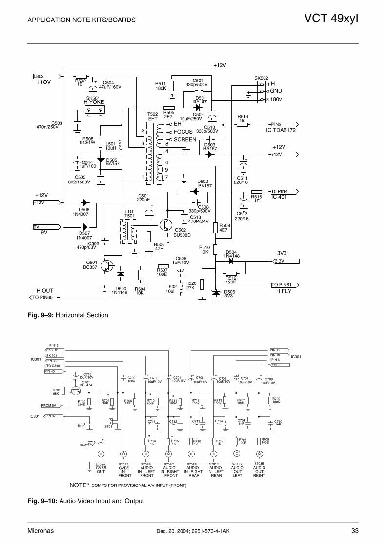
APPLICATION NOTE KITS/BOARDS VCT 49xyI
Fig. 9–9: Horizontal Section
Fig. 9–10: Audio Video Input and Output
H FLYH OUT
9V
+12V
+12V
3 8
6
4
EHT
FOCUSSCREEN
H YOKE
2
197
HGND
180v
11OV
IC 401
3V3
IC TDA8172
+12V
D5063V3
+
C5061uF/10V
1
2
3
SK502C507330p/500V
+
C5141uF/100
D505BA157
D5001N4148
C502470p/63V
C513470P/2KV
C508330p/500V
C510330p/500V
12
SK501
C503470n/250V
C5058n2/1500V
L50110uH
Q501BC337
L50210uH
+
C501220uF
Q502BU508D
+ C50447uF/160V
+
C512220/16
D502BA157
+
C511220/16
D503BA157
+
C50910uF/250V
D501BA157
T501LDT
T502EHT
3.3V
D5041N4148
D5071N4007
D5081N4007
+12V
9V
PIN2
T0 PIN4
TO PIN60
TO PIN61
L802
+12V
R5021E
R52027K
R512120K
R5141E
R5081K5/1W
R511180K
R507100E
R5094E7
R50410K
R50647E
R5052E7
R51010K
R5151E
PIN12
**
OUTCVBSCVBS
*
INAUDIO
NOTE COMPS FOR PROVISIONAL A/V INPUT FRONT
*
*
*
*
*
OUTINFRONT
LEFTAUDIO
IN RIGHTFRONT FRONT
AUDIOIN
REARRIGHT
AUDIOIN LEFT
REAR
AUDIO
LEFT
AUDIO
RIGHTOUT
IC301
IC301
IC301PIN 6
PIN 7
PIN 40
+
C71610uF/10V
S703BS703C
+
C71510uF/10V
Q701BC547A
S703A S702A
FROM 5V
C701100n
C702100n
S701
PIN 37
TO C340
PIN 33
C7101nF
C7091nF
C7141n
C7131n
C7121n
C7111n
+
C70510uF/10V
+
C70610uF/10V
+
C70410uF/10V
S702B S702C S701B S701C
+
C70710uF/10V
+
C70810uF/10V
+
C70310uF/10V
SK301B
SK 301 PIN 10
PIN 11
R70168K
R702220E
R70475E
R70575E
R709180K
R708100E
R707180K
R706100ER714
1KR7151K
R7161K
R7171K
R713100K
R712100K
R711100K
R710100K
Micronas Dec. 20, 2004; 6251-573-4-1AK 33

VCT 49xyI APPLICATION NOTE KITS/BOARDS
Fig. 9–11: Audio
Fig. 9–12: Video AmplifIer
LOT
IC301
MUTE
11V
SP L
SP R
AN7522
5
IC301
IC301
+12V
+
+
C60110uF/10V
TDA7523
1
6
8
9
3117
2
4
10
12
IC601
+
C60510uF/10V
C607100n
+C606100uF/25V
SP6018E
SP6028E
SK601
+
C60010uF/10V
C6031nF
C6021nF
TO PIN5
TO PIN4
FROM 11V
TO C410
TO R514
TO PIN56
L601
R60622kR605
10kR6022K2
R6043K3
TDA7523
C60410uF/10V
TDA6107/9
GRB
3
654
21
GND AQUA GND AQUA
GND
BCL5V
R
G
B
180vGND
H
R/OUT
G/OUT
B/OUT
GND AQUA
EHT
Q901BC547
1
2
3
SK901
D902BA157
D901BA157
D900BA157
+
C90010u/250V
RGB
H
4 15
G1 G2
986
1110
5 7
SK903CRT SOCKET
9
8
7
6
5
4
3
2
1
IC901
Q900BC557
+
C9084u7/250V
C906100n
C9042P2
C9032P2
C9052P2
SK902
C907150p
C9022n2/2KV
D9031N4007
C9012n2/1kv
R9051k
R9061k
R9071k
R9111K2
R9101K2
R9121K2
R9153M3
R9094K7
R925220E
R9175K6
R9141K5
R9041K5
R9131k
34 Dec. 20, 2004; 6251-573-4-1AK Micronas

APPLICATION NOTE KITS/BOARDS VCT 49xyI
10. Annex B
10.1.Photos
Fig. 10–1: Separate Power Supply for the PVB
Fig. 10–2: Priyanka with Power Supply Built-in
Micronas Dec. 20, 2004; 6251-573-4-1AK 35

Micronas GmbHHans-Bunte-Strasse 19D-79108 Freiburg (Germany)P.O. Box 840D-79008 Freiburg (Germany)Tel. +49-761-517-0Fax +49-761-517-2174E-mail: [email protected]: www.micronas.com
Printed in GermanyOrder No. 6251-573-4-1AK
All information and data contained in this document are without anycommitment, are not to be considered as an offer for conclusion of acontract, nor shall they be construed as to create any liability. Any newissue of this data sheet invalidates previous issues. Product availabilityand delivery are exclusively subject to our respective order confirmationform; the same applies to orders based on development samples deliv-ered. By this publication, Micronas GmbH does not assume responsibil-ity for patent infringements or other rights of third parties which mayresult from its use.Further, Micronas GmbH reserves the right to revise this publicationand to make changes to its content, at any time, without obligation tonotify any person or entity of such revisions or changes. No part of this publication may be reproduced, photocopied, stored on aretrieval system, or transmitted without the express written consent ofMicronas GmbH.
VCT 49xyI APPLICATION NOTE KITS/BOARDS
36 Dec. 20, 2004; 6251-573-4-1AK Micronas
11. Application Note History
1. Application Note Kits/Boards: “VCT 49XYI Eco CTV Design with DSP Technology”, Dec. 20, 2004, 6251-573-4-1AK. First release of the application note kits/boards.


![Zunanja in notranja gladka jeklena vrata · Razpoložljive vrste vrat: ECO-DSp-1 - vrata (D), gladka jeklena (Sp), enokrilna (1]; ECO-DSp-2 - vrata (D), gladka jeklena (Sp), dvokrilna](https://img.pdfslide.net/doc/110x75/60d4f4bcc5a549543a1edced/zunanja-in-notranja-gladka-jeklena-vrata-razpololjive-vrste-vrat-eco-dsp-1-.jpg)