Embed Size (px)
Citation preview
Vector Multiplication &
Color ConvolutionTeam Members
Vinay ChintaSreenivas Patil
EECC - 731VLSI Design Projects
Dr. Ken Hsu
Goal
A VLSI chip capable of 3*3 matrix multiplication or 3*3 digital convolution
Design to operate at a frequency suitable for real-time video and image processing applications.
Applications
Typically used in applications such as digital copiers where incoming color data needs to undergo unsharp masking for quality color output.
Data is converted into chrominance and luminance channels.
The RGB signals captured by the camera are linearly matrixed and processed for color sensitivity correction using 3*3 matrices.
After this, convolution operation is applied to luminance channel to enhance sharpness.
Multi-functionality Noise reduction, feature extraction, image
enhancement, restoration and various other operations performed by linear filter (3*3 convolvers)
Providing different kernels or matrices, it can be used for all these image processing operations.
The VMCC is the single solution for all these functions.
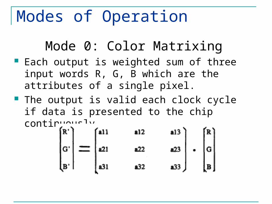
Modes of Operation
Mode 0: Color Matrixing Each output is weighted sum of three input words R,
G, B which are the attributes of a single pixel. The output is valid each clock cycle if data is
presented to the chip continuously
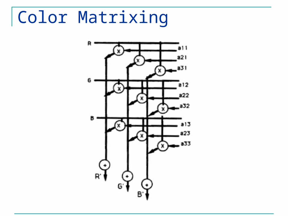
Color Matrixing
Modes of operation
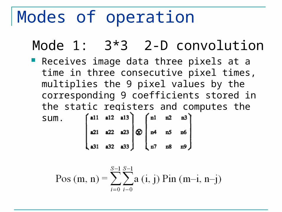
Mode 1: 3*3 2-D convolution Receives image data three pixels at a time in three
consecutive pixel times, multiplies the 9 pixel values by the corresponding 9 coefficients stored in the static registers and computes the sum.
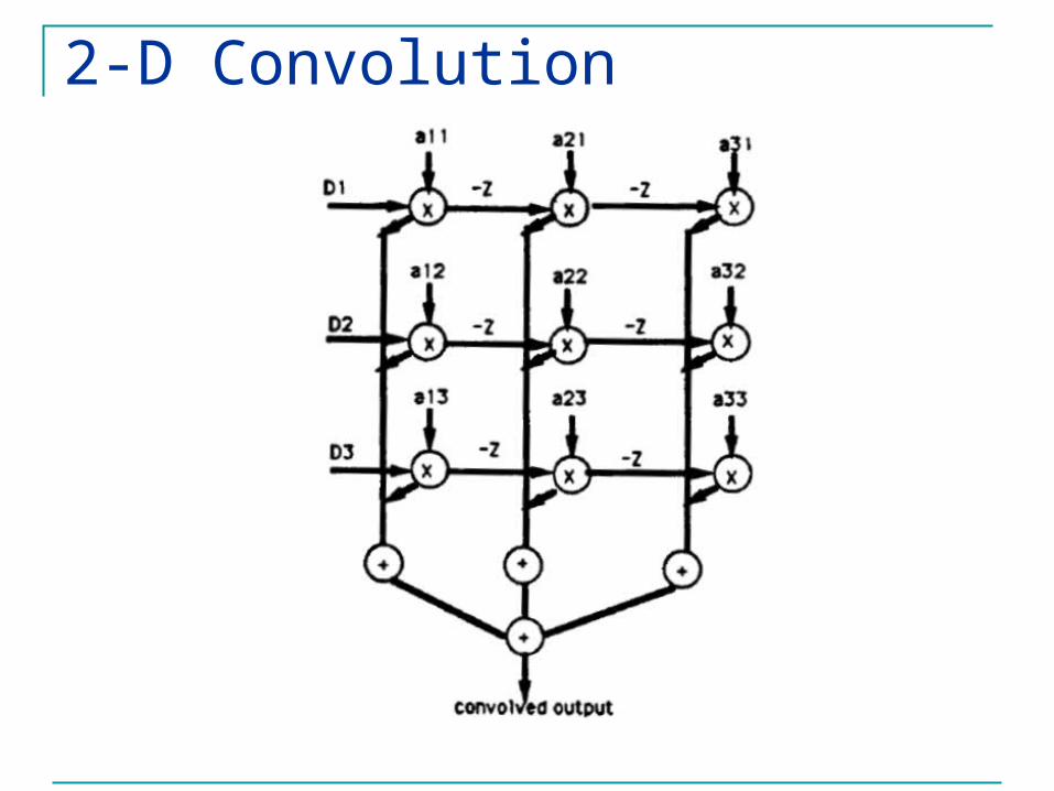
2-D Convolution
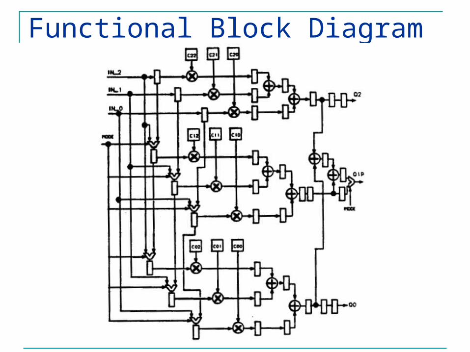
Functional Block Diagram
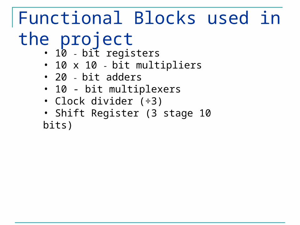
Functional Blocks used in the project
• 10 - bit registers• 10 x 10 - bit multipliers• 20 - bit adders • 10 - bit multiplexers • Clock divider (÷3)• Shift Register (3 stage 10 bits)
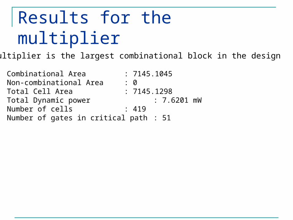
Results for the multiplier
Multiplier is the largest combinational block in the design
Combinational Area : 7145.1045Non-combinational Area : 0 Total Cell Area : 7145.1298Total Dynamic power : 7.6201 mWNumber of cells : 419Number of gates in critical path : 51
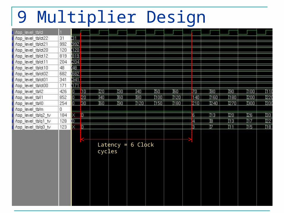
9 Multiplier Design
Latency = 6 Clock cycles
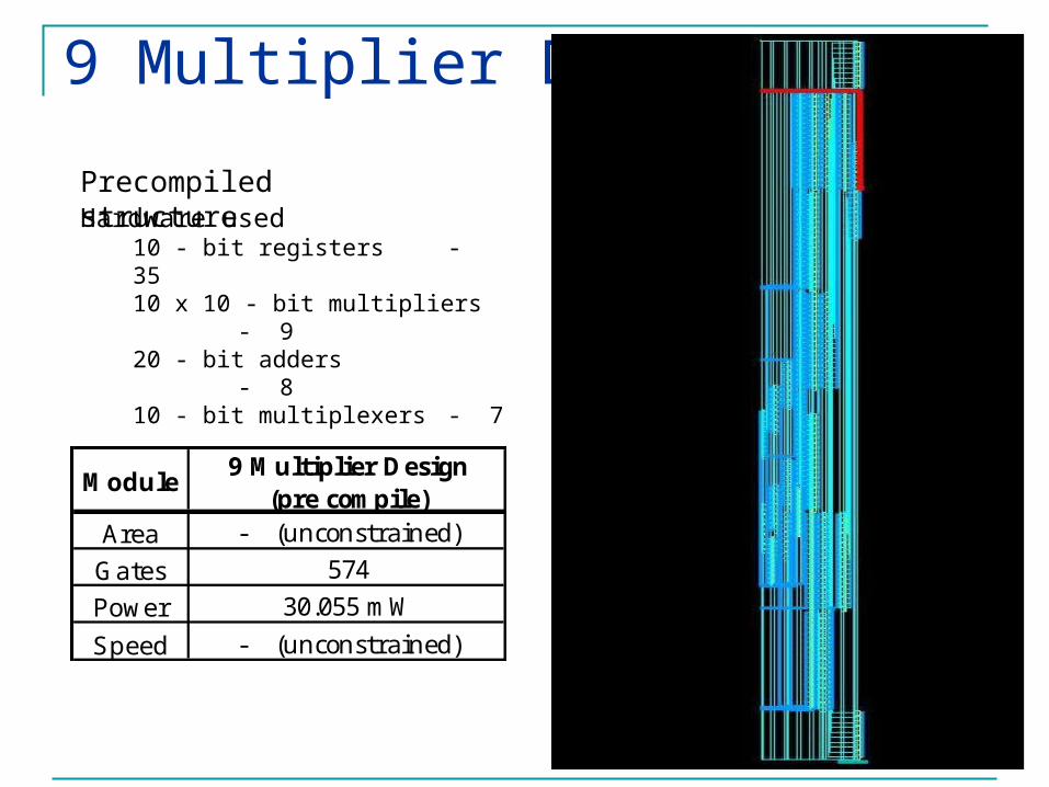
9 Multiplier Design
Precompiled structure
Hardware used10 - bit registers - 3510 x 10 - bit multipliers - 920 - bit adders - 810 - bit multiplexers - 7
Module9 Multiplier Design
(pre compile)Area - (unconstrained)
Gates 574
Power 30.055 mW
Speed - (unconstrained)
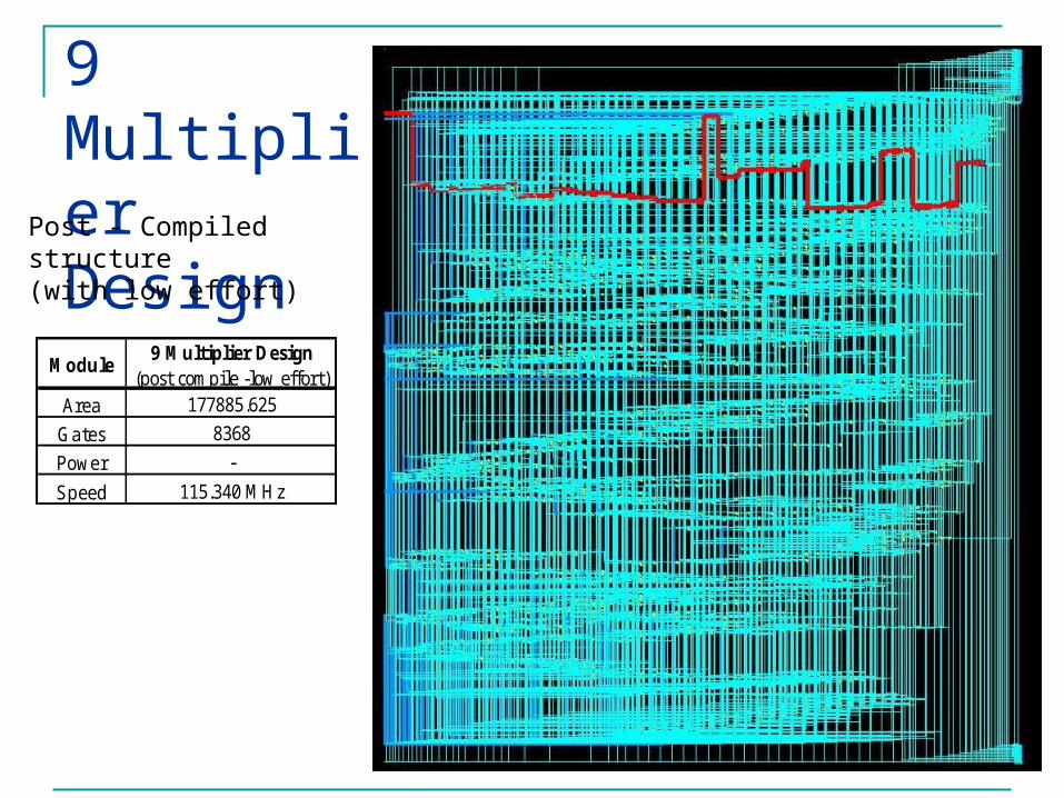
9 Multiplier DesignPost - Compiled structure
(with low effort)
Module9 Multiplier Design
(post compile -low effort)Area 177885.625
Gates 8368
Power -
Speed 115.340 MHz
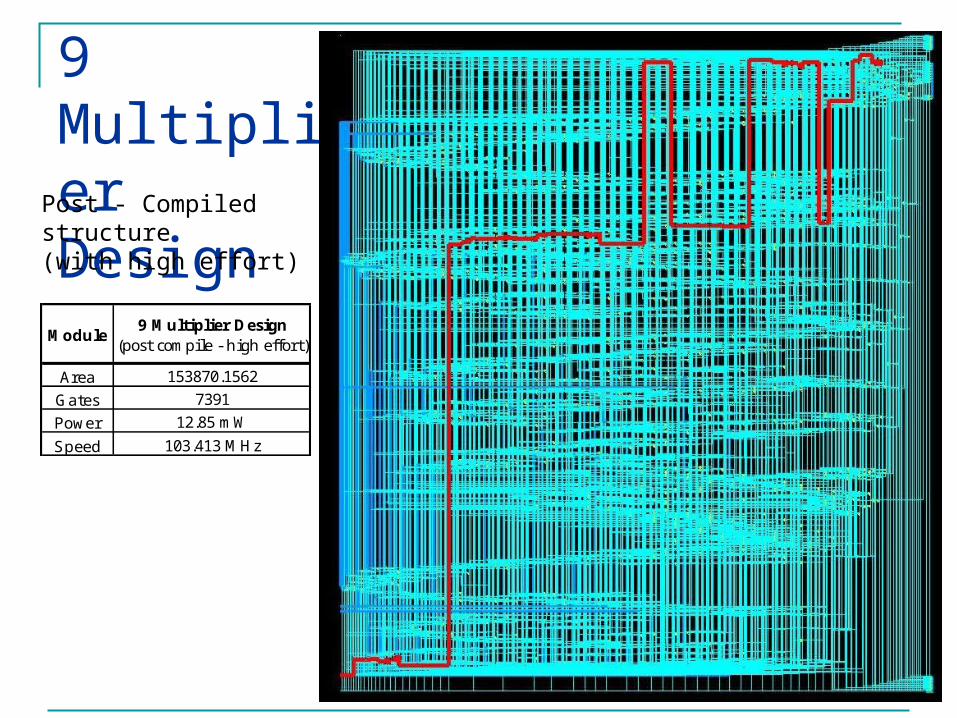
9 Multiplier DesignPost - Compiled structure
(with high effort)
Module9 Multiplier Design
(post compile - high effort)
Area 153870.1562
Gates 7391
Power 12.85 mW
Speed 103.413 MHz
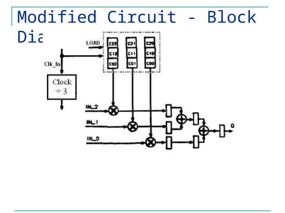
Modified Circuit - Block Diagram
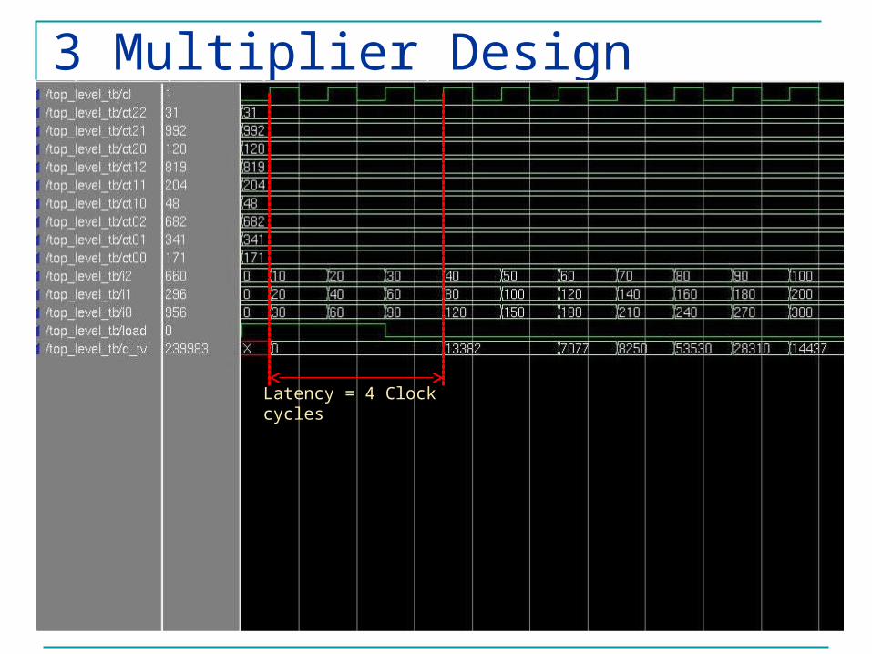
3 Multiplier Design
Latency = 4 Clock cycles
3 Multiplier Design
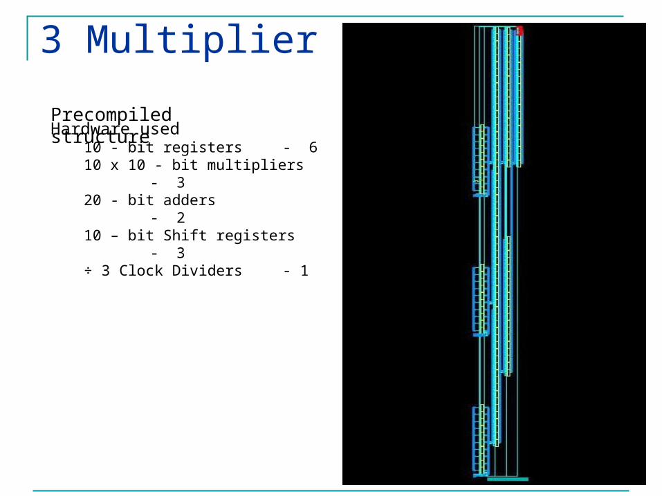
Precompiled structure
Hardware used10 - bit registers - 610 x 10 - bit multipliers - 320 - bit adders - 210 – bit Shift registers - 3÷ 3 Clock Dividers - 1
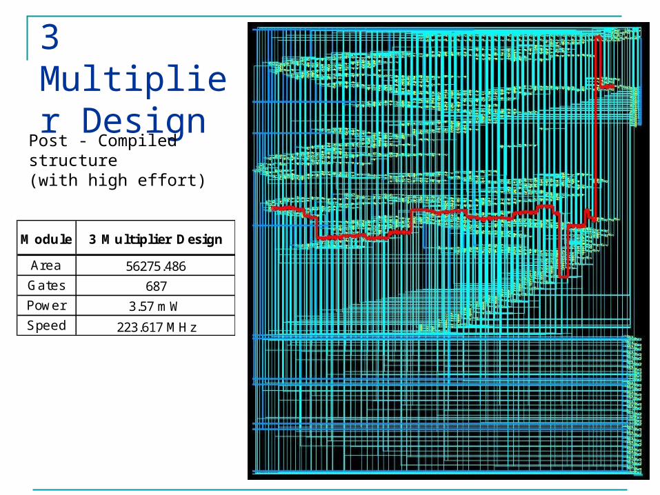
3 Multiplier Design
Post - Compiled structure(with high effort)
Module 3 Multiplier Design
Area 56275.486
Gates 687
Power 3.57 mW
Speed 223.617 MHz
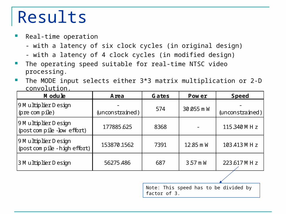
Real-time operation
- with a latency of six clock cycles (in original design)
- with a latency of 4 clock cycles (in modified design) The operating speed suitable for real-time NTSC video processing. The MODE input selects either 3*3 matrix multiplication or 2-D convolution.
Results
Module Area Gates Power Speed
9 Multiplier Design (pre compile)
- (unconstrained)
574 30.055 mW-
(unconstrained)
9 Multiplier Design (post compile -low effort)
177885.625 8368 - 115.340 MHz
9 Multiplier Design (post compile - high effort)
153870.1562 7391 12.85 mW 103.413 MHz
3 Multiplier Design 56275.486 687 3.57 mW 223.617 MHz
Note: This speed has to be divided by factor of 3.
Features
Two operations on a single chip. Matrix operations for color processing Convolution for filtering and enhancement. Real-time operation for NTSC signals.
Further Work
Design of BIST for the design. Control Interface / Communicator Implementation of High Speed Multiplication
and Additions algorithms. Optimize for Higher Speed
References1. A Pipelined ASIC for Color Matrixing and Convolution, K. Hsu, LJ. D'Luna, H. Yeh, W.A. Cook, G.W. Brown2. L. J. D'Luna, et al., A Digital Video Signal Post-Processor for Color Image Sensors, Proceedings of CICC 1989.24.2014.3. Digital integrated circuits : a design perspective , Rabaey,Pearson Education, c20034. W. Wesley Peterson and E. J. Weldon, Jr., Error-Corecting Codes (2nd ed.) 1972, The MIT Press,Cambridge, Massachusetts, 1972,5. VHDL : Programming By Example, Perry, Douglas L, McGraw-Hill, c20026. 3x3 Convolver with Run-Time Reconfigurable Vector Multiplier in Atmel AT6000 FPGAs. AT6000 FPGAs. Application Note (http://www.tecnun.com/asignaturas/tratamiento%20digital/convolver.pdf)7. Digital Image Processing, Gonzalez, Rafael C., Woods, E. Richards. 20028. Introduction To VLSI Circuits And Systems, John P. Uyemura, 1952, J. Wiley, c20029. Fundamentals of digital logic with VHDL design, Brown, Stephen D, McGraw-Hill, c200010. Wikipedia, the free encyclopedia (http://en.wikipedia.org)

Questions ???