Embed Size (px)
Citation preview
Spec
ifica
tions
Version
03.00
November
2006
Vector Signal Generator ¸SMATE200ASpecifications
Vector Signal Generator R&S®SMATE200A Version 03.00, November 2006 2
CONTENTS Introduction.................................................................................................................................................................................................4 Key features ...............................................................................................................................................................................................4 Frequency and enhancement options ........................................................................................................................................................5
Frequency options ..................................................................................................................................................................................5 Enhancement options .............................................................................................................................................................................5
Modulation ..................................................................................................................................................................................................6 Possible modulation types ......................................................................................................................................................................6 Simultaneous modulation........................................................................................................................................................................6
RF characteristics.......................................................................................................................................................................................7 Frequency ...............................................................................................................................................................................................7 Frequency sweep....................................................................................................................................................................................7 Reference frequency...............................................................................................................................................................................7 Level .......................................................................................................................................................................................................9 Level sweep ..........................................................................................................................................................................................12 Spectral purity .......................................................................................................................................................................................12 List mode ..............................................................................................................................................................................................15 Hardware I/O.........................................................................................................................................................................................15
Analog modulation....................................................................................................................................................................................16 Internal modulation generator ...............................................................................................................................................................16 Input for external modulation signals ....................................................................................................................................................16 Amplitude modulation ...........................................................................................................................................................................16 Wideband amplitude modulation...........................................................................................................................................................17 Pulse modulation ..................................................................................................................................................................................17 Frequency modulation (option R&S®SMATE-B22) ...............................................................................................................................17 Phase modulation (option R&S®SMATE-B22) ......................................................................................................................................18
I/Q modulation ..........................................................................................................................................................................................19 I/Q modulator ........................................................................................................................................................................................19 External wideband I/Q...........................................................................................................................................................................19 Internal baseband I/Q (with option R&S®SMATE-B13).........................................................................................................................20 Differential I/Q output (option R&S®SMATE-B16).................................................................................................................................22 I/Q baseband generator (option R&S®SMATE-B9/-B10/-B11) – arbitrary waveform mode..................................................................23 I/Q baseband generator (option R&S®SMATE-B9/-B10/-B11) – realtime operation.............................................................................25 I/Q baseband generator (option R&S®SMATE-B9/-B10/-B11) – realtime operation.............................................................................25 Modulation uncertainty for main standards (typical values) ..................................................................................................................28
Digital modulation systems.......................................................................................................................................................................29 Digital standard GSM/EDGE (option R&S®SMATE-K40) .....................................................................................................................29 Digital standard 3GPP FDD (option R&S®SMATE-K42).......................................................................................................................31 3GPP FDD enhanced BS/MS test including HSDPA (option R&S®SMATE-K43) ................................................................................38 Digital standard GPS (option R&S®SMATE-K44) .................................................................................................................................40 3GPP FDD HSUPA (option R&S®SMATE-K45) ...................................................................................................................................41 Digital standard CDMA2000® incl. 1xEV-DV (option R&S®SMATE-K46) .............................................................................................43
Version 03.00, November 2006 Vector Signal Generator R&S®SMATE200A 3
Digital standard IEEE 802.11 a/b/g (option R&S®SMATE-K48)............................................................................................................46 Digital standard IEEE 802.16 WiMAX including IEEE 802.16e (option R&S®SMATE-K49) .................................................................48 Digital standard TD-SCDMA (3GPP TDD LCR) (option R&S®SMATE-K50) ........................................................................................50 TD-SCDMA (3GPP TDD LCR) enhanced BS/MS test including HSDPA (option R&S®SMATE-K51)..................................................52 Digital standard DVB-H (option R&S®SMATE-K52)..............................................................................................................................53 Multicarrier CW signal generation (option R&S®SMATE-K61)..............................................................................................................54
Digital standards with R&S®WinIQSIM™ (for R&S®SMATE-B9/-B10/-B11 ARB)....................................................................................56 Noise ........................................................................................................................................................................................................56
Additive white Gaussian noise (AWGN, option R&S®SMATE-K62) .....................................................................................................56 General data.............................................................................................................................................................................................57
Remote control......................................................................................................................................................................................57 Operating data ......................................................................................................................................................................................57
Ordering information.................................................................................................................................................................................58
Specifications apply under the following conditions:
30 minutes warm-up time at ambient temperature, specified environmental conditions met, calibration cycle adhered to and all internal adjustments performed. Data designated "overrange", "underrange" and data without tolerance limits is not binding.
EMC specifications are tested with sufficiently shielded cables and accessories (e.g. mouse and keypad). To prevent degradation of these specifications, the user is responsible for using appropriate equipment.
In compliance with the 3GPP standard, chip rates are specified in Mcps (million chips per second), whereas bit rates and symbol rates are specified in kbps (thousand bits per second) or ksps (thousand symbols per second). Mcps, kbps and ksps are not SI units.
Vector Signal Generator R&S®SMATE200A Version 03.00, November 2006 4
Introduction Based on the successful R&S®SMU200A platform, the R&S®SMATE200A is specifically designed for production environments. As such, the display and front panel user interface have been removed, the connectors moved to the rear, and performance has been optimized for fastest setting times to improve factory throughput. Like the R&S®SMU200A, however, the two-generators-in-one concept has been kept, occupying four height units – a plus for production where space is at a premium. All of this is available without compromising the excellent RF performance and baseband flexibility synonymous with the R&S®SMU200A.
Speaking of flexibility, the modular design concept of the R&S®SMATE200A means that the R&S®SMATE200A can easily be adapted to the needs of any application. Users have the choice of either 3 GHz or 6 GHz RF outputs in one or two paths and may opt for up to two completely independent baseband sources. As in the R&S®SMU200A, these sources may be used to produce complex signals in realtime or output preloaded waveforms from the internal arbitrary waveform generator.
In addition to its inherent speed, the R&S®SMATE200A also offers a special function to permit fast switching between different test signals. The multisegment waveform function allows users to easily combine waveforms, such as GSM and WCDMA, during test setup for even faster tests in production. This is just one of the R&S®SMATE200A’s numerous adaptations to the special requirements of the production environment.
Key features Designed for production
• Very short setting times for frequency and level (e.g. for frequency changes <1 ms over GPIB and <400 μs in List mode) • Fast Hop mode offering flexibly addressable frequency/level pairs; as fast as normal List mode • Multisegment waveform function enables fast switching between different test signals in waveform generator • Special hardware triggers for basic functions • Electronic CMOS-attenuator for entire frequency and level range • Status LEDs on front, connectors on rear • Revised cooling concept for longer life in production
Outstanding signal quality
• Very low SSB phase noise (typ. –135 dBc (1 Hz) at f = 1 GHz, 20 kHz offset; typ. –139 dBc (1 Hz) with the enhanced phase noise option)
• Wideband noise of typ. –153 dBc (>5 MHz carrier offset, f = 1 GHz, 1 Hz measurement bandwidth) • High output power up to +19 dBm (PEP), typ. +26 dBm with high-power output option • Very high level repeatability of typ. 0.05 dB • I/Q modulator with 200 MHz RF bandwidth • Excellent ACLR performance of typ. +71 dB with 3GPP FDD
Two signal generators in one
• Up to two completely independent signal generators in one unit • Choice of 3 GHz or 6 GHz frequency options in one or two paths • Up to two independent baseband sources that not only support realtime signal generation but also offer arbitrary waveform
generation with up to 128 Msamples each
Connectivity
• Remote-controllable via LAN (Gigabit Ethernet), GPIB and USB • User-definable triggers and markers combined in one SCSI connector • USB connectors for keyboard, mouse and memory stick • VGA connector for an external display
Version 03.00, November 2006 Vector Signal Generator R&S®SMATE200A 5
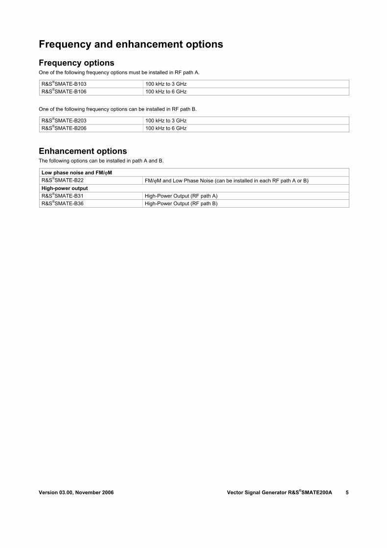
Frequency and enhancement options Frequency options One of the following frequency options must be installed in RF path A.
R&S®SMATE-B103 100 kHz to 3 GHz R&S®SMATE-B106 100 kHz to 6 GHz
One of the following frequency options can be installed in RF path B.
R&S®SMATE-B203 100 kHz to 3 GHz R&S®SMATE-B206 100 kHz to 6 GHz
Enhancement options The following options can be installed in path A and B.
Low phase noise and FM/ϕM R&S®SMATE-B22 FM/ϕM and Low Phase Noise (can be installed in each RF path A or B) High-power output R&S®SMATE-B31 High-Power Output (RF path A) R&S®SMATE-B36 High-Power Output (RF path B)
Vector Signal Generator R&S®SMATE200A Version 03.00, November 2006 6
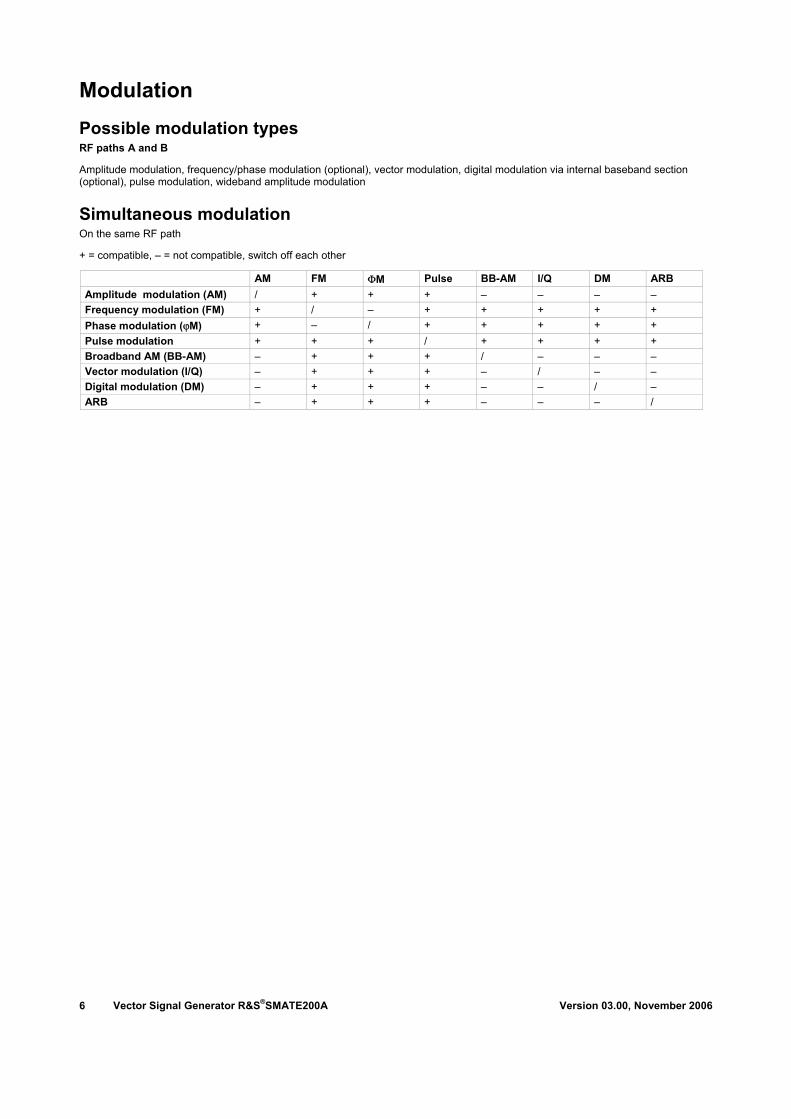
Modulation Possible modulation types RF paths A and B
Amplitude modulation, frequency/phase modulation (optional), vector modulation, digital modulation via internal baseband section (optional), pulse modulation, wideband amplitude modulation
Simultaneous modulation On the same RF path
+ = compatible, – = not compatible, switch off each other
AM FM ΦM Pulse BB-AM I/Q DM ARB Amplitude modulation (AM) / + + + – – – – Frequency modulation (FM) + / – + + + + + Phase modulation (ϕM) + – / + + + + + Pulse modulation + + + / + + + + Broadband AM (BB-AM) – + + + / – – – Vector modulation (I/Q) – + + + – / – – Digital modulation (DM) – + + + – – / – ARB – + + + – – – /
Version 03.00, November 2006 Vector Signal Generator R&S®SMATE200A 7
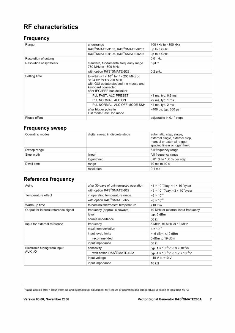
RF characteristics Frequency
underrange 100 kHz to <300 kHz R&S®SMATE-B103, R&S®SMATE-B203 up to 3 GHz
Range
R&S®SMATE-B106, R&S®SMATE-B206 up to 6 GHz Resolution of setting 0.01 Hz
standard, fundamental frequency range 750 MHz to 1500 MHz
5 µHz Resolution of synthesis
with option R&S®SMATE-B22 0.2 µHz to within <1 × 10⁻⁷ for f > 200 MHz or <124 Hz for f < 200 MHz, with GUI update stopped, no mouse and keyboard connected after IEC/IEEE bus delimiter
PLL FAST, ALC PRESET1 <1 ms, typ. 0.6 ms PLL NORMAL, ALC ON <2 ms, typ. 1 ms PLL NORMAL, ALC OFF MODE S&H <4 ms, typ. 2 ms
Setting time
after trigger pulse in List mode/Fast Hop mode
<400 µs, typ. 300 µs
Phase offset adjustable in 0.1° steps
Frequency sweep Operating modes digital sweep in discrete steps automatic, step, single,
external single, external step, manual or external trigger, spacing linear or logarithmic
Sweep range full frequency range linear full frequency range Step width logarithmic 0.01 % to 100 % per step range 10 ms to 10 s Dwell time resolution 0.1 ms
Reference frequency after 30 days of uninterrupted operation <1 × 10⁻⁹/day, <1 × 10⁻⁷/year Aging with option R&S®SMATE-B22 <5 × 10⁻¹⁰/day, <3 × 10⁻⁸/year in operating temperature range <6 × 10⁻⁸ Temperature effect with option R&S®SMATE-B22 <6 × 10⁻⁹
Warm-up time to nominal thermostat temperature ≤10 min frequency (approx. sinewave) 10 MHz or external input frequency level typ. 5 dBm
Output for internal reference signal
source impedance 50 Ω frequency 5 MHz, 10 MHz or 13 MHz maximum deviation 3 × 10⁻⁶
input level, limits >–6 dBm, ≤19 dBm recommended 0 dBm to 19 dBm
Input for external reference
input impedance 50 Ω sensitivity typ. 1 × 10⁻⁸/V to 3 × 10⁻⁸/V
with option R&S®SMATE-B22 typ. 4 × 10⁻⁹/V to 1.2 × 10⁻⁸/V input voltage –10 V to +10 V
Electronic tuning from input AUX I/O
input impedance 10 kΩ
1 Value applies after 1 hour warm-up and internal level adjustment for 4 hours of operation and temperature variation of less than +5 °C.
Vector Signal Generator R&S®SMATE200A Version 03.00, November 2006 8
0 0.5 1 1.5 2 2.50
500
1000
1500
2000
2500
t/ms
n
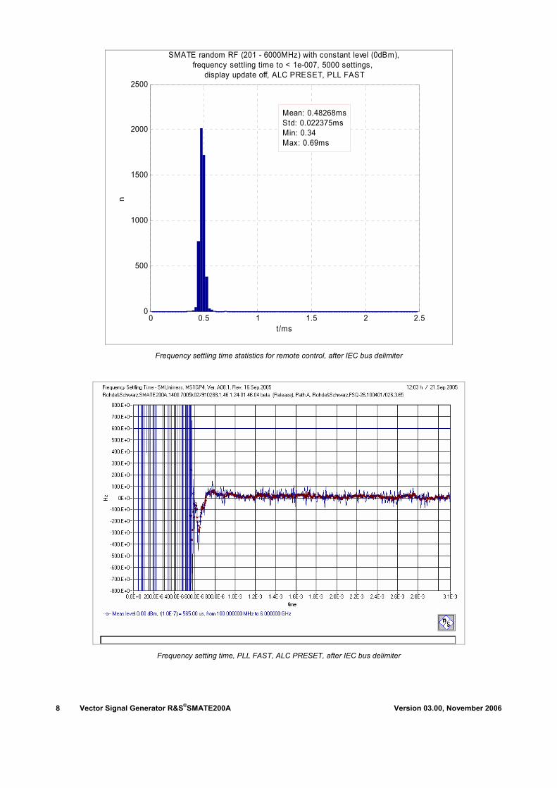
SMATE random RF (201 - 6000MHz) with constant level (0dBm),frequency settling time to < 1e-007, 5000 settings,
display update off, ALC PRESET, PLL FAST
Mean: 0.48268msStd: 0.022375msMin: 0.34Max: 0.69ms
Frequency settling time statistics for remote control, after IEC bus delimiter
Frequency setting time, PLL FAST, ALC PRESET, after IEC bus delimiter
Version 03.00, November 2006 Vector Signal Generator R&S®SMATE200A 9
Level standard −145 dBm to +20 dBm Setting range with option R&S®SMATE-B31 or R&S®SMATE-B36
to +30 dBm
standard f ≤ 3 GHz +13 dBm (PEP)2 f > 3 GHz +11 dBm (PEP)
with option R&S®SMATE-B31 or R&S®SMATE-B36
f ≤ 3 GHz +19 dBm (PEP) f > 3 GHz +17 dBm (PEP)
Maximum level
resolution 0.01 dB for levels >−120 dBm, attenuator mode "auto", temperature range +18 °C to +33 °C
1 MHz ≤ f ≤ 3 GHz <0.5 dB
Level uncertainty
f > 3 GHz <0.9 dB Additional uncertainty with ALC OFF, S&H
This function is needed only in some special applications.
<0.2 dB
ALC state ON, standard f ≤ 3 GHz <1.6, typ. <1.4 f > 3 GHz <1.85, typ. <1.6
ALC state ON, with options R&S®SMATE-B31 or R&S®SMATE-B36
attenuator mode "normal" f ≤ 3 GHz <1.65, typ. <1.45 f > 3 GHz <1.9, typ. <1.65
attenuator mode "high power" f ≤ 3 GHz <1.7, typ. <1.5
Output impedance VSWR in 50 Ω system
f > 3 GHz <1.9, typ. <1.65 after IEC/IEEE bus delimiter, with GUI update stopped, no mouse and keyboard connected, temperature range +18 °C to +33 °C
to <0.1 dB deviation from final value PLL FAST, ALC PRESET3 <1 ms, typ. 0.6 ms PLL NORMAL, ALC ON <2 ms, typ. 1.1 ms PLL NORMAL, ALC OFF <4 ms, typ. 2.5 ms
after trigger in List mode/Fast Hop mode
to <0.3 dB deviation from final value <450 µs , typ. 300 µs to <0.1 dB deviation from final value <800 µs , typ. 400 µs
Setting time
range switch-over with option R&S®SMATE-B31 or R&S®SMATE-B36
<10 ms
Uninterrupted level setting with attenuator mode fixed, ALC state on setting range
>20 dB
maximum permissible RF power in output frequency range of RF path for f > 1 MHz
1 MHz < f ≤ 3 GHz 50 W 3 GHz < f ≤ 6 GHz 10 W
Back-feed (from ≥50 Ω source)
maximum permissible DC voltage 50 V
2 PEP = peak envelope power. 3 Value applies after 1 hour warm-up and internal level adjustment for 4 hours of operation and temperature variation of less than +5 °C.
Vector Signal Generator R&S®SMATE200A Version 03.00, November 2006 10
0.5 1 1.5 2 2.5 3 3.5 4 4.5 5 5.5 6
x 109
10
12
14
16
18
20
22
24
26
28
30
RF frequency / Hz
Leve
l / d
Bm
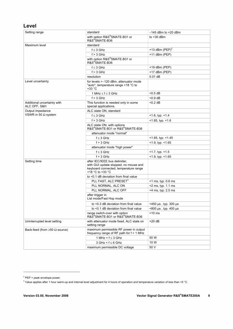
Max. available output power with frequency option B106,Attenuator Mode Normal (lower trace) and High Power (upper trace)
0.5 1 1.5 2 2.5 3
x 109
10
12
14
16
18
20
22
24
26
28
30
RF frequency / Hz
Leve
l / d
Bm
Max. available output power with frequency option B103,Attenuator Mode Normal (lower trace) and High Power (upper trace)
Measured maximum available output level versus frequency
Measured level versus frequency at 0 dBm
Version 03.00, November 2006 Vector Signal Generator R&S®SMATE200A 11
0 0.5 1 1.5 2 2.50
500
1000
1500
2000
2500
t/ms
n
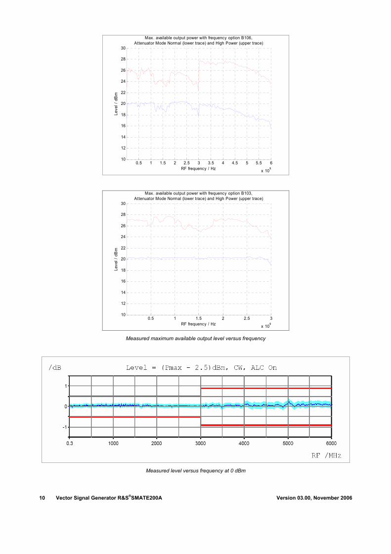
SMATE random level (-35 - 13 dBm) with constant RF (2200 MHz)level settling to < 0.1 dB from final value, 5000 settings, display update off
Mean: 0.42908msStd: 0.072823msMin: 0Max: 0.625ms
Level setting time statistics for remote control, after IEC bus delimiter
Level repeatability with random settings between measurements, modulation 3GPP test model 1, 64 channels
Vector Signal Generator R&S®SMATE200A Version 03.00, November 2006 12
Level sweep Operating modes digital sweep in discrete steps auto, single, step,
extern single, extern step manual or external trigger
Sweep range level range of attenuator modes "normal" or "high power"
Step width logarithmic 0.1 dB to 20 dB per step range 10 ms to 10 s Dwell time resolution 0.1 ms
Spectral purity standard, unmodulated
level <8 dBm <–30 dBc level <13 dBm typ.<–30 dBc
Harmonics
with options R&S®SMATE-B31or R&S®SMATE-B36A, unmodulated, level <12 dBm
<–30 dBc
level >–50 dBm, CW, vector modulation (full-scale DC input), >10 kHz offset from carrier and outside the modulation spectrum
0.3 MHz ≤ f ≤ 200 MHz <–77 dBc 200 MHz < f ≤ 1500 MHz <–80 dBc 1500 MHz < f ≤ 3000 MHz <–74 dBc f > 3000 MHz <–68 dBc
>850 kHz offset from carrier and outside the modulation spectrum
0.3 MHz ≤ f ≤ 200 MHz <–77 dBc
200 MHz ≤ f ≤ 1500 MHz <–86 dBc 1500 MHz ≤ f ≤ 3000 MHz <–80 dBc
Nonharmonics
f > 3000 MHz <–74 dBc level > –50 dBm, CW, vector modulation (full-scale DC input), >10 kHz offset from carrier and outside the modulation spectrum
0.3 MHz ≤ f ≤ 200 MHz <–77 dBc, typ. –87 dBc 200 MHz < f ≤ 1500 MHz <–90 dBc 1500 MHz < f ≤ 3000 MHz <–84 dBc
Nonharmonics with option R&S®SMATE-B22
f > 3000 MHz <–78 dBc Power supply and mechanically related nonharmonics
at RF = 1 GHz, 50 Hz to 10 kHz from the carrier
<–70 dBc
1.5 GHz < f ≤ 3 GHz <–74 dBc Subharmonics 3 GHz < f ≤ 6 GHz <–50 dBc carrier offset >10 MHz, measurement bandwidth 1 Hz, CW
20 MHz ≤ f ≤ 200 MHz <–146 dBc, typ. –149 dBc 200 MHz < f ≤ 1500 MHz <–150 dBc, typ. –153 dBc 1.5 GHz < f ≤ 3 GHz <–148 dBc, typ. –151 dBc f > 3 GHz <–146 dBc, typ. –149 dBc
vector modulation with full-scale DC input, I/Q input gain 3 dB
20 MHz ≤ f ≤ 200 MHz <–143 dBc, typ. –146 dBc 200 MHz < f ≤ 1500 MHz <–146 dBc, typ. –149 dBc 1.5 GHz < f ≤ 3 GHz <–145 dBc, typ. –148 dBc
Wideband noise
f > 3 GHz <–143 dBc, typ. –146 dBc
Version 03.00, November 2006 Vector Signal Generator R&S®SMATE200A 13
carrier offset 20 kHz, measurement bandwidth 1 Hz, unmodulated
PLL mode NORMAL 20 MHz ≤ f ≤ 200 MHz <–128 dBc, typ. –132 dBc f = 1 GHz <–131 dBc, typ. –135 dBc f = 2 GHz <–125 dBc, typ. –129 dBc f = 3 GHz <–121 dBc, typ. –125 dBc f = 4 GHz <–119 dBc, typ. –123 dBc f = 6 GHz <–115 dBc, typ. –119 dBc
PLL mode FAST 20 MHz ≤ f ≤ 200 MHz <–127 dBc, typ. –131 dBc f = 1 GHz <–130 dBc, typ. –134 dBc f = 2 GHz <–124 dBc, typ. –128 dBc f = 3 GHz <–120 dBc, typ. –124 dBc f = 4 GHz <–118 dBc, typ. –122 dBc
SSB phase noise
f = 6 GHz <–114 dBc, typ. –118 dBc carrier offset 20 kHz, measurement bandwidth 1 Hz
20 MHz ≤ f ≤ 200 MHz <–135 dBc, typ. –138 dBc f = 1 GHz <–136 dBc, typ. –139 dBc f = 2 GHz <–130 dBc, typ. –133 dBc f = 3 GHz <–126 dBc, typ. –129 dBc f = 4 GHz <–124 dBc, typ. –127 dBc
SSB phase noise with option R&S®SMATE-B22
f = 6 GHz <–120 dBc, typ. –123 dBc rms value at f = 1 GHz
300 Hz to 3 kHz <1 Hz Residual FM
20 Hz to 23 kHz <4 Hz Residual AM rms value 20 Hz to 23 kHz <0.02 %
Vector Signal Generator R&S®SMATE200A Version 03.00, November 2006 14
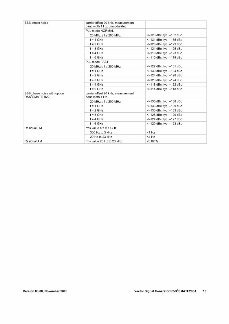
Measured SSB phase noise, I/Q modulated (typical values)
-170
-160
-150
-140
-130
-120
-110
-100
-90
-80
-70
-60
-50
-40
1,0E+00 1,0E+01 1,0E+02 1,0E+03 1,0E+04 1,0E+05 1,0E+06 1,0E+07Offset frequency / Hz
SSB
pha
se n
oise
/ dB
c (1
Hz
mea
s. b
andw
idth
)
5.7 GHz
2.1 GHz
850 MHz
100 MHz
Measured SSB phase noise, unmodulated (typical values)
-170
-160
-150
-140
-130
-120
-110
-100
-90
-80
-70
-60
-50
-40
1,0E+00 1,0E+01 1,0E+02 1,0E+03 1,0E+04 1,0E+05 1,0E+06 1,0E+07Offset frequency / Hz
SSB
pha
se n
oise
/ dB
c (1
Hz
mea
s. b
andw
idth
)
5.7 GHz
2.1 GHz
850 MHz
100 MHz
Measured SSB phase noise with Option B22, unmodulated (typical values)
-170
-160
-150
-140
-130
-120
-110
-100
-90
-80
-70
-60
-50
-40
1,0E+00 1,0E+01 1,0E+02 1,0E+03 1,0E+04 1,0E+05 1,0E+06 1,0E+07Offset frequency / Hz
SSB
pha
se n
oise
/ dB
c (1
Hz
mea
s. b
andw
idth
)
5.7 GHz
2.1 GHz
850 MHz
100 MHz
Version 03.00, November 2006 Vector Signal Generator R&S®SMATE200A 15
List mode Frequency and level values can be stored in a list and set in an extremely short amount of time. Operating modes automatic, single sweep, manual or
external trigger, fast hopping with immediate and external trigger
Max. number of channels 10000 Dwell time 1 ms to 20 s
Resolution 0.1 ms Setting time after external trigger see frequency and level data additional trigger delay in two-path units,
both operated in List mode/Fast Hop mode<200 µs
Hardware I/O Hardware control lines for direct and fast access to instrument functions
level LVTTL OPC A/B Output for operation complete signal of path A/B
response time typ. 10 μs
level LVTTL RF OFF A/B Input for fast switching of RF output A/B response time typ. 10 μs
Vector Signal Generator R&S®SMATE200A Version 03.00, November 2006 16
Analog modulation The R&S®SMATE200A has two EXT MOD inputs for independent analog modulation of both RF paths.
Internal modulation generator Frequency range 0.1 Hz to 1 MHz Resolution of setting 0.1 Hz Frequency uncertainty <0.012 Hz +
relative deviation of reference frequency up to 100 kHz <0.1 dB Frequency response up to 1 MHz <1 dB
Distortion up to 100 kHz at RL > 200 Ω, level (Vp) 1 V <0.1 % Vp at LF connector, RL > 200 Ω 1 mV to 3 V resolution 1 mV
Output voltage
setting uncertainty at 1 kHz <(1 % of reading + 1 mV) Output impedance 16 Ω Frequency setting time to within <1 × 10⁻⁷, with GUI update
stopped, after IEC/IEEE bus delimiter <3 ms
digital sweep in discrete steps operating modes automatic, step, single, external single,
external step, manual or extern trigger, spacing linear or logarithmic
sweep range full frequency range step width linear full frequency range
Sweep
step width logarithmic 0.01 % to 100 % per step
Input for external modulation signals input impedance
high (>100 kΩ), switchable to 50 Ω with option R&S®SMATE-B22
input sensitivity (peak value for set modulation depth or deviation)
1 V
Modulation input EXT MOD A/B
absolute maximum rating 10 V
Amplitude modulation Operating modes internal, external AC/DC
at high levels, modulation is clipped, if the maximum PEP is reached
0 % to 100 % Modulation depth
resolution 0.1 % Setting uncertainty attenuator mode "auto",
fmod = 1 kHz and m <80 % <(1 % of reading +1 %)
PEP in specified range, attenuator mode "auto"
f ≤ 3 GHz, at fmod = 1 kHz m = 30 % <0.5 % m = 80 % <0.8 %
f > 3 GHz, at fmod = 1 kHz,
m = 30 % <1 %
AM distortion
m = 80 % <1.6 % Modulation frequency range DC, 20 Hz to 500 kHz Modulation frequency response mode AC, 20 Hz to 500 kHz <1 dB Incidental φM at AM m = 30 %, fmod = 1 kHz, peak value <0.1 rad
Version 03.00, November 2006 Vector Signal Generator R&S®SMATE200A 17
Wideband amplitude modulation Operating modes modulation input I external DC Modulation frequency response as with I/Q modulation –
external wideband I/Q
Input impedance 50 Ω Input sensitivity peak voltage for 100 % AM 0.25 V
Pulse modulation Operating modes external
internal (duty cycle approx. 1:1) ON/OFF ratio >70 dB Rise/fall time 10 %/90 % of RF amplitude typ. 1 µs Pulse repetition frequency 0 Hz to 100 kHz Video crosstalk spectral line of fundamental of
100 kHz squarewave modulation <−30 dBc
input level rising 1.7 V, falling typ. 1.1 V input impedance >10 kΩ
Modulation input EXT MOD A/B
polarity selectable
Frequency modulation (option R&S®SMATE-B22) Operating modes internal, external, internal + external,
AC/DC, "Normal", "Low Noise"
f ≤ 200 MHz 1 200 MHz < f ≤ 375 MHz rm = 0.25 375 MHz < f ≤ 750 MHz rm = 0.5 750 MHz < f ≤ 1500 MHz rm = 1 1500 MHz < f ≤ 3000 MHz rm = 2
FM/ϕM range multiplier
f > 3000 MHz rm = 4 FM mode "Normal" rm × 10 MHz FM mode "Low Noise" rm × 100 kHz
Maximum deviation
resolution <200 ppm, min. rm × 0.1 Hz fmod = 10 kHz, deviation ≤ half of max.
internal <(1.5 % of reading + 20 Hz) Setting uncertainty
external <(2.0 % of reading + 20 Hz) 40 kHz deviation, fmod = 1 kHz, f > 5 MHz <0.1 % Synchronous AM f > 3 GHz <0.2 %
FM distortion fmod = 10 kHz and 1 MHz deviation <0.1 % FM mode "Normal"
10 Hz to 100 kHz <0.5 dB 10 Hz to 10 MHz <3 dB
FM mode "Low Noise"
Modulation frequency response
10 Hz to 100 kHz <3 dB 40 kHz deviation, fmod = 1 kHz, f > 5 MHz <0.1 % Synchronous AM f > 3 GHz <0.2 %
Carrier frequency offset at FM <0.2 % of set deviation
Vector Signal Generator R&S®SMATE200A Version 03.00, November 2006 18
Phase modulation (option R&S®SMATE-B22) Operating mode internal, external, internal + external,
AC/DC, "High Bandwidth, "High Deviation", "Low Noise"
ϕM mode "High Deviation" rm × 20.0 rad ϕM mode "High Bandwidth" rm × 1.0 rad
Maximum deviation
ϕM mode "Low Noise" rm × 0.25 rad ϕM mode "High Deviation" <200 ppm, min. rm × 20 µrad ϕM mode "High Bandwidth" <0.1 %, min. rm x 20 µrad
Resolution
ϕM mode "Low Noise" <200 ppm, min. rm × 20 µrad fmod = 10 kHz, deviation ≤ half of max.
internal <(1.5 % of reading + 0.01 rad) Setting uncertainty
external <(2.0 % of reading + 0.01 rad) ϕM distortion fmod = 10 kHz, half of max. deviation <0.2 %, typ. 0.1 %
"High Deviation", 10 Hz to 500 kHz <1 dB "High Bandwidth", 10 Hz to 10 MHz <3 dB
Modulation frequency response
"Low Noise", 10 Hz to 100 kHz <3 dB
Version 03.00, November 2006 Vector Signal Generator R&S®SMATE200A 19
I/Q modulation I/Q modulator Operating modes external wideband I/Q,
internal baseband I/Q I offset, Q offset
setting range −10 % to +10 % resolution 0.01 %
gain imbalance setting range −1.0 to +1.0 dB resolution 0.001 dB
quadrature offset setting range −10° to +10°
I/Q impairments
resolution 0.01° I/Q swap I and Q signals swapped OFF, ON
External wideband I/Q The R&S®SMATE200A has two I/Q inputs for independent I/Q modulation of both RF paths.
input impedance 50 Ω VSWR up to 50 MHz <1.2 input voltage for full-scale input
q2 2i + = 0.5 VV V
I/Q inputs
minimum input voltage for ALC state on
0.1 V
Modulation frequency range IQ wideband on 100 MHz IQ wideband set to on up to 50 MHz typ. <6 dB
RF frequency response for entire instrument in modulation bandwidth
up to 5 MHz typ. <1.0 dB Carrier leakage without input signal, referenced to full-
scale input4 <−55 dBc, typ. <−65 dBc
measured with 16QAM, filter root cosine, α = 0.5, symbol rate 10 kHz
rms value f ≤ 200 MHz <0.3 % f > 200 MHz <(0.2 % + 0.1 % × f/GHz)
peak value f ≤ 200 MHz <0.6 %
Error vector
f > 200 MHz <(0.4 % + 0.2 % × f/GHz)
4 Value applies after 1 hour warm-up and recalibration for 4 hours operation and temperature variations of less than +5 °C.
Vector Signal Generator R&S®SMATE200A Version 03.00, November 2006 20
Delta
/ dB
5
4
3
2
1
0
–1
– 2
– 3
– 4
– 5
Frequency offset from carrier / MHz
– 100 1000 60– 20– 60 20 40 80– 80 – 40
RF 850 MHzRF 1900 MHzRF 2200 MHz
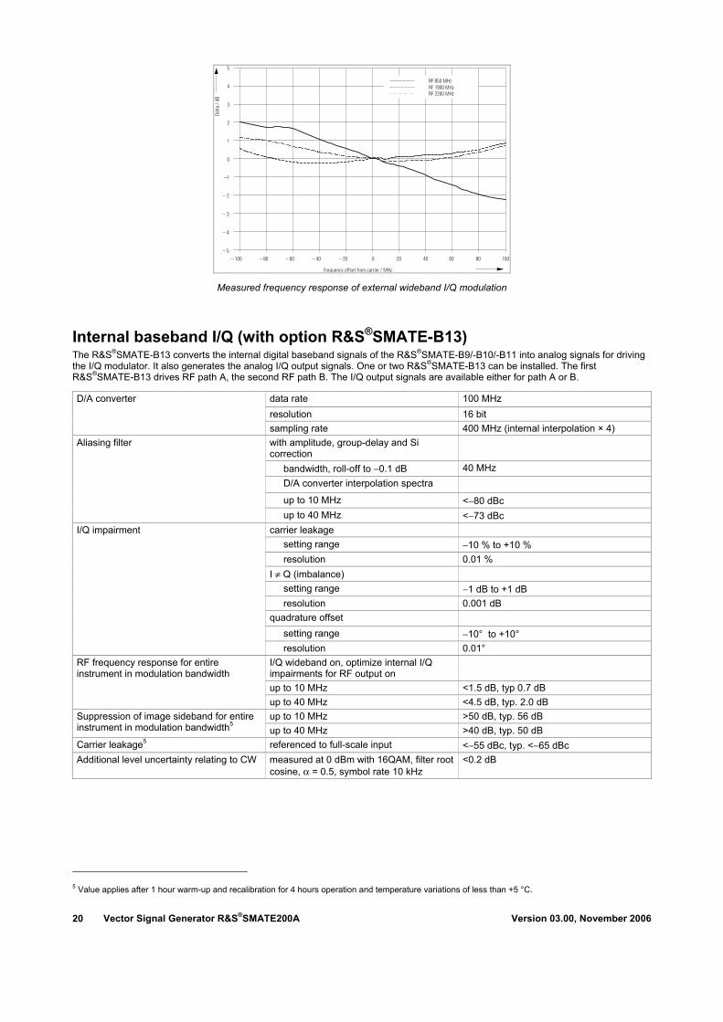
Measured frequency response of external wideband I/Q modulation
Internal baseband I/Q (with option R&S®SMATE-B13) The R&S®SMATE-B13 converts the internal digital baseband signals of the R&S®SMATE-B9/-B10/-B11 into analog signals for driving the I/Q modulator. It also generates the analog I/Q output signals. One or two R&S®SMATE-B13 can be installed. The first R&S®SMATE-B13 drives RF path A, the second RF path B. The I/Q output signals are available either for path A or B.
data rate 100 MHz resolution 16 bit
D/A converter
sampling rate 400 MHz (internal interpolation × 4) with amplitude, group-delay and Si correction
bandwidth, roll-off to −0.1 dB 40 MHz D/A converter interpolation spectra
up to 10 MHz <−80 dBc
Aliasing filter
up to 40 MHz <−73 dBc carrier leakage
setting range −10 % to +10 % resolution 0.01 %
I ≠ Q (imbalance) setting range −1 dB to +1 dB resolution 0.001 dB
quadrature offset setting range −10° to +10°
I/Q impairment
resolution 0.01° I/Q wideband on, optimize internal I/Q impairments for RF output on
up to 10 MHz <1.5 dB, typ 0.7 dB
RF frequency response for entire instrument in modulation bandwidth
up to 40 MHz <4.5 dB, typ. 2.0 dB up to 10 MHz >50 dB, typ. 56 dB Suppression of image sideband for entire
instrument in modulation bandwidth5 up to 40 MHz >40 dB, typ. 50 dB Carrier leakage5 referenced to full-scale input <−55 dBc, typ. <−65 dBc Additional level uncertainty relating to CW measured at 0 dBm with 16QAM, filter root
cosine, α = 0.5, symbol rate 10 kHz <0.2 dB
5 Value applies after 1 hour warm-up and recalibration for 4 hours operation and temperature variations of less than +5 °C.
Version 03.00, November 2006 Vector Signal Generator R&S®SMATE200A 21
I/Q outputs Output impedance 50 Ω Output voltage EMF
output voltage depends on set modulation signal
1 V (Vp)
Offset EMF <1 mV at RL = 50 Ω magnitude
up to 10 MHz typ. 0.02 dB up to 40 MHz typ. 0.03 dB
nonlinear phase up to 10 MHz typ. 0.1°
Frequency response6
up to 30 MHz typ. 0.2° at RL = 50 Ω magnitude
up to 10 MHz typ. 0.01 dB up to 40 MHz typ. 0.02 dB
nonlinear phase up to 10 MHz typ. 0.1°
I/Q balance
up to 30 MHz typ. 0.2° at RL = 50 Ω SFDR (sine)
up to 2 MHz >70 dB up to 20 MHz typ. 60 dB
phase noise 10 MHz sinewave at 20 kHz offset typ. −150 dBc
wideband noise
Spectral purity
10 MHz sinewave at 1 MHz offset typ. −155 dBc
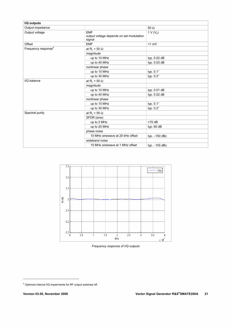
Frequency response of I/Q outputs
6 Optimize internal I/Q impairments for RF output switched off.
Vector Signal Generator R&S®SMATE200A Version 03.00, November 2006 22
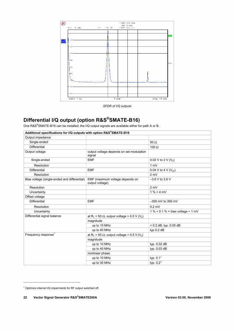
SFDR of I/Q outputs
Differential I/Q output (option R&S®SMATE-B16) One R&S®SMATE-B16 can be installed; the I/Q output signals are available either for path A or B.
Additional specifications for I/Q outputs with option R&S®SMATE-B16 Output impedance
Single-ended 50 Ω Differential 100 Ω
Output voltage output voltage depends on set modulation signal
Single-ended EMF 0.02 V to 2 V (Vp)
Resolution 1 mV Differential EMF 0.04 V to 4 V (Vpp)
Resolution 2 mV Bias voltage (single-ended and differential) EMF (maximum voltage depends on
output voltage) –3.6 V to 3.6 V
Resolution 2 mV Uncertainty 1 % + 4 mV
Offset voltage Differential EMF –300 mV to 300 mV
Resolution 0.2 mV Uncertainty 1 % + 0.1 % × bias voltage + 1 mV
at RL = 50 Ω, output voltage > 0.5 V (Vp) magnitude
up to 10 MHz < 0.2 dB, typ. 0.05 dB
Differential signal balance
up to 40 MHz typ 0.2 dB at RL = 50 Ω, output voltage > 0.5 V (Vp) magnitude
up to 10 MHz typ. 0.02 dB up to 40 MHz typ. 0.03 dB
nonlinear phase up to 10 MHz typ. 0.1°
Frequency response7
up to 30 MHz typ. 0.2°
7 Optimize internal I/Q impairments for RF output switched off.
Version 03.00, November 2006 Vector Signal Generator R&S®SMATE200A 23
I/Q baseband generator (option R&S®SMATE-B9/-B10/-B11) – arbitrary waveform mode At least one Baseband Main Module R&S®SMATE-B13 must be installed. One or two R&S®SMATE-B9/-B10/-B11 can be installed. Their I/Q signals can be assigned a frequency offset and/or be added in the digital domain.
output memory waveform length R&S®SMATE-B9 128 sample to 128 Msample in
one-sample steps waveform length R&S®SMATE-B10 128 sample to 64 Msample in one-sample
steps waveform length R&S®SMATE-B11 128 sample to 16 Msample in one-sample
steps resolution 16 bit loading time 10 Msample 15 s
Waveform memory
nonvolatile memory hard disk number of segments max. 100 segments changeover modes GUI, remote control, external trigger extended trigger modes same segment, next segment, next
segment seamless changeover time (external trigger, without clock change)
typ. 5 μs
Multisegment waveform
seamless changeover output up to end of current segment, followed by changeover to next segment
number of carriers max. 32 total RF bandwidth max. 80 MHz crest factor modes maximize, minimize, off signal period modes longest file, shortest file, user (max. 1 s) single carrier gain –80 dB to 0 dB single carrier start phase 0° to 360°
Multicarrier waveform
single carrier delay 0 s to 1 s clock rate 400 Hz to 100 MHz resolution 0.001 Hz operating mode internal, external
Clock generation
frequency uncertainty (internal) <5 × 10⁻¹⁴ × clock rate + uncertainty of reference frequency
The sampling rate of the waveform is automatically interpolated to the internal 100 MHz data rate.
bandwidth clock rate =100 MHz (no interpolation), roll-off to –0.1 dB
40 MHz
Interpolation
clock rate ≤100 MHz, drop to −0.1 dB 0.31 × clock rate With the aid of the frequency offset, the center frequency of the wanted baseband signal can be shifted. The restrictions caused by the modulation bandwidth still apply.
range −40 MHz to +40 MHz resolution 0.01 Hz
Frequency offset
frequency uncertainty <5 × 10 − 10 × frequency offset + reference frequency error
Vector Signal Generator R&S®SMATE200A Version 03.00, November 2006 24
In internal clock mode, a trigger event restarts the clock generation. The clock phase is then synchronous with the trigger (with a certain timing uncertainty). In external clock mode the trigger event is synchronized to the symbol clock.
operating mode internal, external modes Auto, Retrig, Armed Auto, Armed Retrig setting uncertainty for clock phase related to trigger in internal clock mode
<18 ns
external trigger delay setting range 0 sample to (216 – 1) sample resolution
internal clock mode 0.01 sample external clock mode 1 sample
setting uncertainty <5 ns external trigger inhibit
setting range 0 sample to (226 – 1) sample resolution 1 sample
external trigger pulse width >15 ns
Triggering
external trigger frequency <0.02 × sampling rate number 4 level LVTTL operating modes unchanged, restart, pulse, pattern, ratio marker delay
setting range 0 sample to (waveform length − 1) sample setting range without recalculation 0 sample to 2000 sample resolution of setting 0.001 sample
Marker outputs
setting uncertainty <10 ns Operation with R&S®WinIQSIM™: As of version 4.10, the software supports download of I/Q data and control of the R&S®SMATE-B10/-B11.
Version 03.00, November 2006 Vector Signal Generator R&S®SMATE200A 25
I/Q baseband generator (option R&S®SMATE-B9/-B10/-B11) – realtime operation At least one Baseband Main Module R&S®SMATE-B13 must be installed. One or two R&S®SMATE-B9/-B10/-B11 can be installed. Their I/Q signals can be assigned a frequency offset and/or be added.
ASK modulation index 0 % to 100 % resolution 0.1 %
FSK 2FSK, 4FSK, MSK deviation 0.1 to 1.5 × fsym
maximum 10 MHz resolution <0.1 Hz setting uncertainty <0.5 %
variable FSK 4FSK, 8FSK, 16FSK deviations –1.5 × fsym to +1.5 × fsym
maximum 10 MHz resolution <0.1 Hz
PSK BPSK, QPSK, QPSK 45° offset, OQPSK, π/4-QPSK, π/2-DBPSK, π/4-DQPSK, π/8-D8PSK, 8PSK, 8PSK EDGE
Types of modulation
QAM 16QAM, 32QAM, 64QAM, 256QAM, 1024QAM
Coding Not all coding methods can be used with every type of modulation.
Off, Differential, Diff. Phase, Diff.+Gray, Gray, GSM, NADC, PDC, PHS, TETRA, APCO25 (PSK), PWT, TFTS, INMARSAT, VDL, EDGE, APCO25(FSK), ICO, CDMA2000®8, WCDMA
Any filter can be used with any type of modulation. The bandwidth of the modulation signal is max. 25 MHz; the signal is clipped if the bandwidth is exceeded.
cosine, root cosine filter parameter α 0.05 to 1.00
Gaussian filter parameter B × T 0.15 to 2.50
cdmaOne, cdmaOne + equalizer cdmaOne 705 kHz, cdmaOne 705 kHz + equalizer CDMA2000® 3x APCO25 C4FM rectangular split phase
filter parameter B × T 0.15 to 2.5
Baseband filter
resolution of filter parameter 0.01 If an external clock is used, the applied data rate may deviate from the set clock rate by ±2 %. The external clock can be used for internal and external data.
operating mode internal, external setting range
ASK, PSK and QAM 400 Hz to 25 MHz FSK 400 Hz to 15 MHz
resolution 0.001 Hz frequency uncertainty (internal) <5 × 10–14 × symbol rate + reference
frequency uncertainty external clock symbol, K × symbol, bit clock clock divider K 1 to 64
Symbol rate
external clock rate max. 100 MHz 8 CDMA2000® is a registered trademark of the Telecommunications Industry Association (TIA-USA).
Vector Signal Generator R&S®SMATE200A Version 03.00, November 2006 26
With the aid of the frequency offset, the center frequency of the modulation signal in the baseband can be shifted. The restrictions caused by the modulation bandwidth apply.
setting range −40 MHz to +40 MHz resolution 0.01 Hz
Frequency offset
frequency uncertainty <5 × 10 − 10 × frequency offset + reference frequency error
internal All 0
All 1 PRBS
sequence length 9, 11, 15, 16, 20, 21, 23 pattern
length 1 bit to 64 bit data lists
output memory 8 bit to 2 Gbit nonvolatile memory hard disk
external In the case of serial transmission, the symbol strobe marks the LSB of the symbol, and the maximum symbol rate is limited by the data rate of the interface.
serial word width 1 bit to 10 bit bit rate max. 60 MHz
parallel word width 1 bit to 10 bit
Data sources
symbol rate max. 25 MHz In internal clock mode, a trigger event restarts the clock generation. The clock phase is then synchronous with the trigger (with a certain timing uncertainty). In external clock mode the trigger event is synchronized to the symbol clock.
operating mode internal, external modes Auto, Retrig, Armed Auto, Armed Retrig setting uncertainty for clock phase related to trigger in internal clock mode
<18 ns
external trigger delay setting range 0 sample to (216 – 1) sample resolution
internal clock mode 0.01 sample external clock mode 1 sample
setting uncertainty <5 ns external trigger inhibit 0 sample to (226 – 1) sample
setting range resolution 1 sample
external trigger pulse width >15 ns
Triggering
external trigger frequency <0.02 × sampling rate number 4 level LVTTL operating modes control list, restart, pulse, pattern, ratio marker delay (in sample)
setting range 0 to 224 – 1 setting range without recalculation 0 to 2000 resolution of setting 0.001
Marker outputs
setting uncertainty <10 ns
Version 03.00, November 2006 Vector Signal Generator R&S®SMATE200A 27
Internal or external via LEVATT input. The signal switches between nominal and reduced level (without edge shaping). If an internal LEVATT signal is used, the connector is used as an output.
setting range 0 dB to 60 dB additional level error in case of reduction
up to 30 dB <1 dB
Level reduction
up to 50 dB <3 dB Internal or external via BURST input. The signal triggers the beginning of a power ramp. The positive edge starts power ramping from blank to full level, the negative edge ramping in the opposite direction from full level to blanking. If an internal BURST GATE signal is applied, the connector is used as an output.
operating range max. 5 MHz rise/fall time
setting range 0.5 symbol to 16 symbol resolution 0.1 symbol
Burst
ramp shape cosine, linear Input impedance and trigger threshold can be set separately for the trigger and the clock/data inputs.
input impedance 1 kΩ, 50 Ω trigger threshold
setting range 0.00 V to 2.50 V
Trigger/clock/data inputs
resolution 0.01 V Clock/data outputs Level LVTTL
modulation, filter, symbol rate and coding to standard
Predefined settings
standards Bluetooth®9, DECT, ETC, GSM, GSM EDGE, NADC, PDC, PHS, TETRA, WCDMA 3GPP, TD-SCDMA, CDMA2000® Forward, CDMA2000® Reverse, Worldspace
Modulation errors deviation 0.2 to 0.7 × symbol rate Gaussian filter with B × T = 0.2 to 0.7
symbol rate up to 2 MHz <1.2 %, typ. 0.25 %
Deviation error with 2FSK, 4FSK
symbol rate up to 10 MHz typ. 0.75 % Gaussian filter with B × T = 0.2 to 0.7
bit rate up to 2 MHz <0.4°, typ. 0.15° Phase error with MSK
bit rate up to 10 MHz typ. 0.3° cosine, root cosine filter with α = 0.2 to 0.7
symbol rate up to 5 MHz <0.8 %, typ. 0.2 % EVM with QPSK, OQPSK, π/4-DQPSK, 8PSK, 16QAM, 32QAM, 64QAM
symbol rate up to 20 MHz typ. 0.7 %
9 The Bluetooth® word mark and logos are owned by the Bluetooth SIG, Inc. and any use of such marks by Rohde & Schwarz is under license.
Vector Signal Generator R&S®SMATE200A Version 03.00, November 2006 28
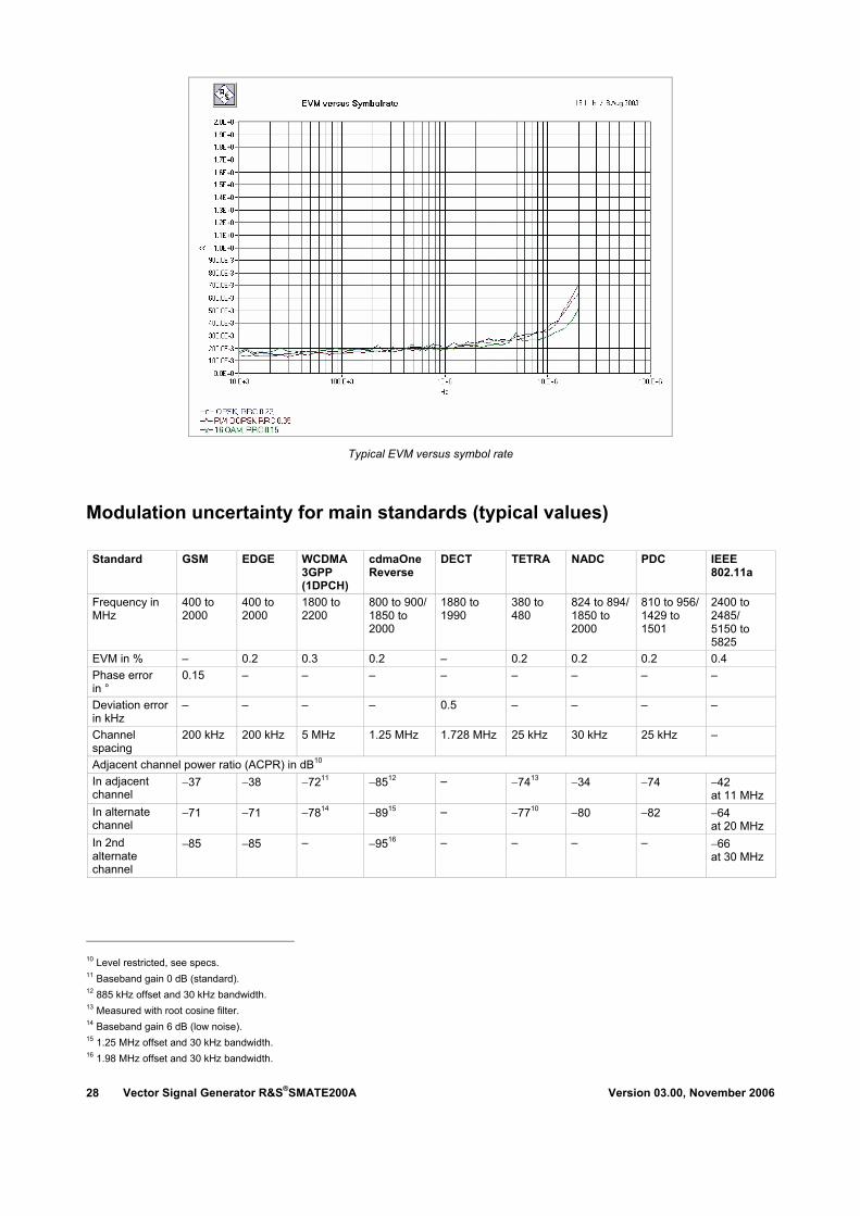
Typical EVM versus symbol rate
Modulation uncertainty for main standards (typical values)
Standard GSM EDGE WCDMA 3GPP (1DPCH)
cdmaOne Reverse
DECT TETRA NADC PDC IEEE 802.11a
Frequency in MHz
400 to 2000
400 to 2000
1800 to 2200
800 to 900/1850 to 2000
1880 to 1990
380 to 480
824 to 894/ 1850 to 2000
810 to 956/ 1429 to 1501
2400 to 2485/ 5150 to 5825
EVM in % – 0.2 0.3 0.2 – 0.2 0.2 0.2 0.4 Phase error in °
0.15 – – – – – – – –
Deviation error in kHz
– – – – 0.5 – – – –
Channel spacing
200 kHz 200 kHz 5 MHz 1.25 MHz 1.728 MHz 25 kHz 30 kHz 25 kHz –
Adjacent channel power ratio (ACPR) in dB10 In adjacent channel
−37 −38 −7211 −8512 – −7413 −34 −74 −42 at 11 MHz
In alternate channel
−71 −71 −7814 −8915 – −7710 −80 −82 −64 at 20 MHz
In 2nd alternate channel
−85 −85 – −9516 – – – – −66 at 30 MHz
10 Level restricted, see specs. 11 Baseband gain 0 dB (standard). 12 885 kHz offset and 30 kHz bandwidth. 13 Measured with root cosine filter. 14 Baseband gain 6 dB (low noise). 15 1.25 MHz offset and 30 kHz bandwidth. 16 1.98 MHz offset and 30 kHz bandwidth.
Version 03.00, November 2006 Vector Signal Generator R&S®SMATE200A 29
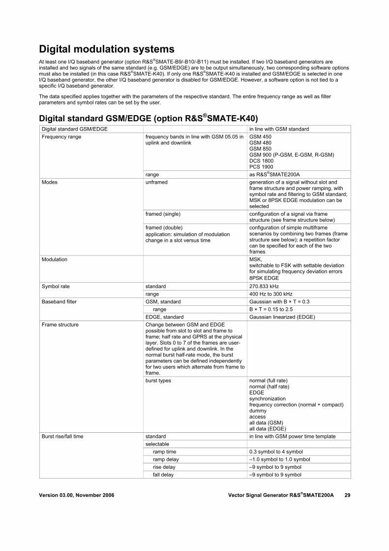
Digital modulation systems At least one I/Q baseband generator (option R&S®SMATE-B9/-B10/-B11) must be installed. If two I/Q baseband generators are installed and two signals of the same standard (e.g. GSM/EDGE) are to be output simultaneously, two corresponding software options must also be installed (in this case R&S®SMATE-K40). If only one R&S®SMATE-K40 is installed and GSM/EDGE is selected in one I/Q baseband generator, the other I/Q baseband generator is disabled for GSM/EDGE. However, a software option is not tied to a specific I/Q baseband generator.
The data specified applies together with the parameters of the respective standard. The entire frequency range as well as filter parameters and symbol rates can be set by the user.
Digital standard GSM/EDGE (option R&S®SMATE-K40) Digital standard GSM/EDGE in line with GSM standard
frequency bands in line with GSM 05.05 in uplink and downlink
GSM 450 GSM 480 GSM 850 GSM 900 (P-GSM, E-GSM, R-GSM) DCS 1800 PCS 1900
Frequency range
range as R&S®SMATE200A unframed generation of a signal without slot and
frame structure and power ramping, with symbol rate and filtering to GSM standard; MSK or 8PSK EDGE modulation can be selected
framed (single) configuration of a signal via frame structure (see frame structure below)
Modes
framed (double) application: simulation of modulation change in a slot versus time
configuration of simple multiframe scenarios by combining two frames (frame structure see below); a repetition factor can be specified for each of the two frames
Modulation MSK, switchable to FSK with settable deviation for simulating frequency deviation errors 8PSK EDGE
standard 270.833 kHz Symbol rate range 400 Hz to 300 kHz GSM, standard Gaussian with B × T = 0.3
range B × T = 0.15 to 2.5 Baseband filter
EDGE, standard Gaussian linearized (EDGE) Change between GSM and EDGE possible from slot to slot and frame to frame; half rate and GPRS at the physical layer. Slots 0 to 7 of the frames are user-defined for uplink and downlink. In the normal burst half-rate mode, the burst parameters can be defined independently for two users which alternate from frame to frame.
Frame structure
burst types normal (full rate) normal (half rate) EDGE synchronization frequency correction (normal + compact) dummy access all data (GSM) all data (EDGE)
standard in line with GSM power time template selectable
ramp time 0.3 symbol to 4 symbol ramp delay –1.0 symbol to 1.0 symbol rise delay –9 symbol to 9 symbol
Burst rise/fall time
fall delay –9 symbol to 9 symbol
Vector Signal Generator R&S®SMATE200A Version 03.00, November 2006 30
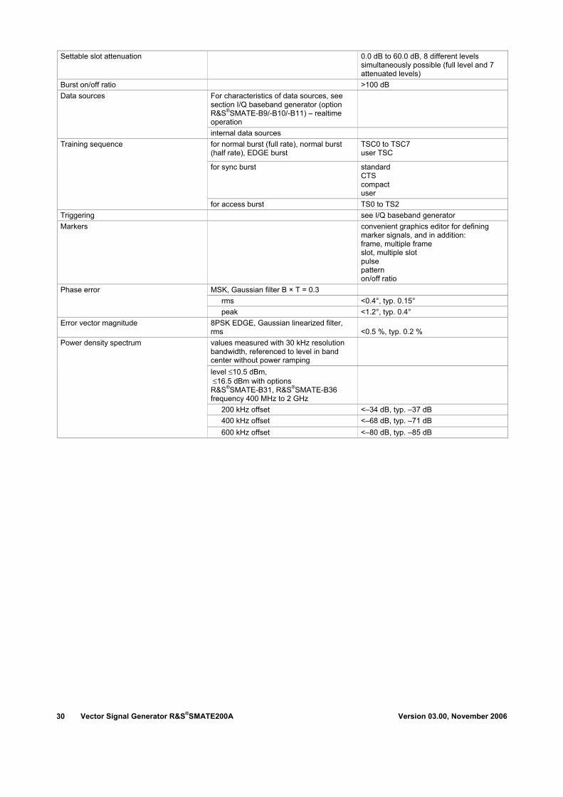
Settable slot attenuation 0.0 dB to 60.0 dB, 8 different levels simultaneously possible (full level and 7 attenuated levels)
Burst on/off ratio >100 dB For characteristics of data sources, see section I/Q baseband generator (option R&S®SMATE-B9/-B10/-B11) – realtime operation
Data sources
internal data sources for normal burst (full rate), normal burst (half rate), EDGE burst
TSC0 to TSC7 user TSC
for sync burst standard CTS compact user
Training sequence
for access burst TS0 to TS2 Triggering see I/Q baseband generator Markers convenient graphics editor for defining
marker signals, and in addition: frame, multiple frame slot, multiple slot pulse pattern on/off ratio
MSK, Gaussian filter B × T = 0.3 rms <0.4°, typ. 0.15°
Phase error
peak <1.2°, typ. 0.4° Error vector magnitude 8PSK EDGE, Gaussian linearized filter,
rms <0.5 %, typ. 0.2 %
values measured with 30 kHz resolution bandwidth, referenced to level in band center without power ramping
level ≤10.5 dBm, ≤16.5 dBm with options R&S®SMATE-B31, R&S®SMATE-B36 frequency 400 MHz to 2 GHz
200 kHz offset <–34 dB, typ. –37 dB 400 kHz offset <–68 dB, typ. –71 dB
Power density spectrum
600 kHz offset <–80 dB, typ. –85 dB
Version 03.00, November 2006 Vector Signal Generator R&S®SMATE200A 31
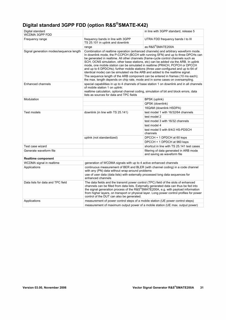
Digital standard 3GPP FDD (option R&S®SMATE-K42) Digital standard WCDMA 3GPP FDD
in line with 3GPP standard, release 5
frequency bands in line with 3GPP TS 25.101 in uplink and downlink
UTRA FDD frequency bands I to III Frequency range
range as R&S®SMATE200A Signal generation modes/sequence length Combination of realtime operation (enhanced channels) and arbitrary waveform mode.
In downlink mode, the P-CCPCH (BCCH with running SFN) and up to three DPCHs can be generated in realtime. All other channels (frame-cycle control channels such as SCH, OCNS simulation, other base stations, etc) can be added via the ARB. In uplink mode, one mobile station can be simulated in realtime (PRACH, PCPCH or DPCCH and up to 6 DPDCHs); further mobile stations (three user-configured and up to 64 of identical mode) can be simulated via the ARB and added to the realtime signal. The sequence length of the ARB component can be entered in frames (10 ms each); the max. length depends on chip rate, mode and in some cases on oversampling.
Enhanced channels special capabilities in up to 4 channels of base station 1 on downlink and in all channels of mobile station 1 on uplink: realtime calculation, optional channel coding, simulation of bit and block errors, data lists as sources for data and TPC fields BPSK (uplink) QPSK (downlink)
Modulation
16QAM (downlink HSDPA) test model 1 with 16/32/64 channels test model 2 test model 3 with 16/32 channels test model 4
downlink (in line with TS 25.141)
test model 5 with 8/4/2 HS-PDSCH channels DPCCH + 1 DPDCH at 60 ksps
Test models
uplink (not standardized) DPCCH + 1 DPDCH at 960 ksps
Test case wizard shortcut in line with TS 25.141 test cases Generate waveform file filtering of data generated in ARB mode
and saving as waveform file Realtime component WCDMA signal in realtime generation of WCDMA signals with up to 4 active enhanced channels Applications continuous measurement of BER and BLER (with channel coding) in a code channel
with any (PN) data without wrap-around problems use of user data (data lists) with externally processed long data sequences for enhanced channels
Data lists for data and TPC field The data fields and the transmit power control (TPC) field of the slots of enhanced channels can be filled from data lists. Externally generated data can thus be fed into the signal generation process of the R&S®SMATE200A, e.g. with payload information from higher layers, on transport or physical layer. Long power control profiles for power control of the DUT can also be generated. measurement of power control steps of a mobile station (UE power control steps) Applications measurement of maximum output power of a mobile station (UE max. output power)
Vector Signal Generator R&S®SMATE200A Version 03.00, November 2006 32
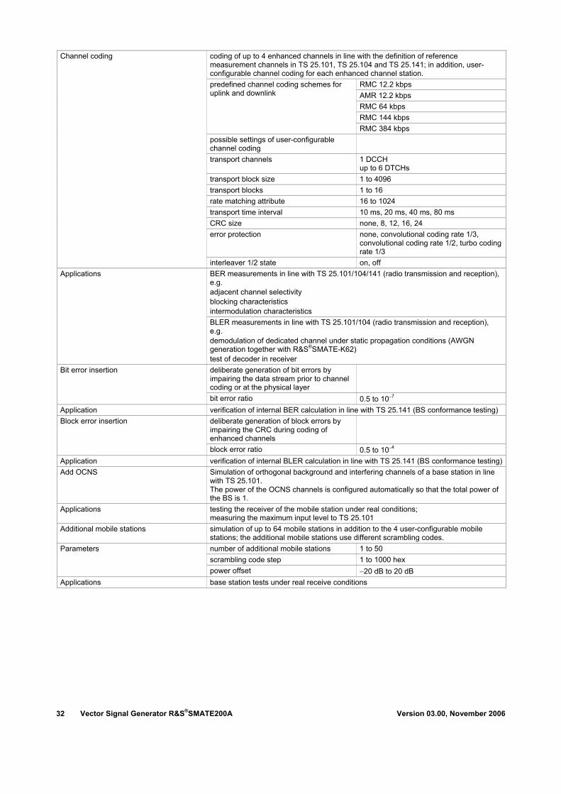
coding of up to 4 enhanced channels in line with the definition of reference measurement channels in TS 25.101, TS 25.104 and TS 25.141; in addition, user-configurable channel coding for each enhanced channel station.
RMC 12.2 kbps AMR 12.2 kbps RMC 64 kbps RMC 144 kbps
predefined channel coding schemes for uplink and downlink
RMC 384 kbps possible settings of user-configurable channel coding
transport channels 1 DCCH up to 6 DTCHs
transport block size 1 to 4096 transport blocks 1 to 16 rate matching attribute 16 to 1024 transport time interval 10 ms, 20 ms, 40 ms, 80 ms CRC size none, 8, 12, 16, 24 error protection none, convolutional coding rate 1/3,
convolutional coding rate 1/2, turbo coding rate 1/3
Channel coding
interleaver 1/2 state on, off BER measurements in line with TS 25.101/104/141 (radio transmission and reception), e.g. adjacent channel selectivity blocking characteristics intermodulation characteristics
Applications
BLER measurements in line with TS 25.101/104 (radio transmission and reception), e.g. demodulation of dedicated channel under static propagation conditions (AWGN generation together with R&S®SMATE-K62) test of decoder in receiver deliberate generation of bit errors by impairing the data stream prior to channel coding or at the physical layer
Bit error insertion
bit error ratio 0.5 to 10−7 Application verification of internal BER calculation in line with TS 25.141 (BS conformance testing)
deliberate generation of block errors by impairing the CRC during coding of enhanced channels
Block error insertion
block error ratio 0.5 to 10−4 Application verification of internal BLER calculation in line with TS 25.141 (BS conformance testing)Add OCNS
Simulation of orthogonal background and interfering channels of a base station in line with TS 25.101. The power of the OCNS channels is configured automatically so that the total power of the BS is 1.
Applications testing the receiver of the mobile station under real conditions; measuring the maximum input level to TS 25.101
Additional mobile stations simulation of up to 64 mobile stations in addition to the 4 user-configurable mobile stations; the additional mobile stations use different scrambling codes. number of additional mobile stations 1 to 50 scrambling code step 1 to 1000 hex
Parameters
power offset −20 dB to 20 dB Applications base station tests under real receive conditions
Version 03.00, November 2006 Vector Signal Generator R&S®SMATE200A 33
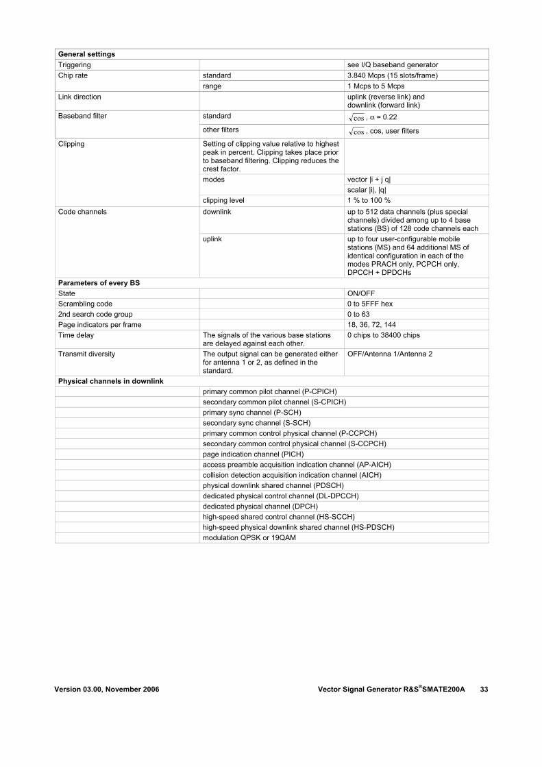
General settings Triggering see I/Q baseband generator
standard 3.840 Mcps (15 slots/frame) Chip rate range 1 Mcps to 5 Mcps
Link direction uplink (reverse link) and downlink (forward link)
standard cos , α = 0.22 Baseband filter
other filters cos , cos, user filters
Setting of clipping value relative to highest peak in percent. Clipping takes place prior to baseband filtering. Clipping reduces the crest factor.
vector |i + j q| modes scalar |i|, |q|
Clipping
clipping level 1 % to 100 % downlink up to 512 data channels (plus special
channels) divided among up to 4 base stations (BS) of 128 code channels each
Code channels
uplink up to four user-configurable mobile stations (MS) and 64 additional MS of identical configuration in each of the modes PRACH only, PCPCH only, DPCCH + DPDCHs
Parameters of every BS State ON/OFF Scrambling code 0 to 5FFF hex 2nd search code group 0 to 63 Page indicators per frame 18, 36, 72, 144 Time delay The signals of the various base stations
are delayed against each other. 0 chips to 38400 chips
Transmit diversity The output signal can be generated either for antenna 1 or 2, as defined in the standard.
OFF/Antenna 1/Antenna 2
Physical channels in downlink primary common pilot channel (P-CPICH) secondary common pilot channel (S-CPICH) primary sync channel (P-SCH) secondary sync channel (S-SCH) primary common control physical channel (P-CCPCH) secondary common control physical channel (S-CCPCH) page indication channel (PICH) access preamble acquisition indication channel (AP-AICH) collision detection acquisition indication channel (AICH) physical downlink shared channel (PDSCH) dedicated physical control channel (DL-DPCCH) dedicated physical channel (DPCH) high-speed shared control channel (HS-SCCH) high-speed physical downlink shared channel (HS-PDSCH) modulation QPSK or 19QAM
Vector Signal Generator R&S®SMATE200A Version 03.00, November 2006 34
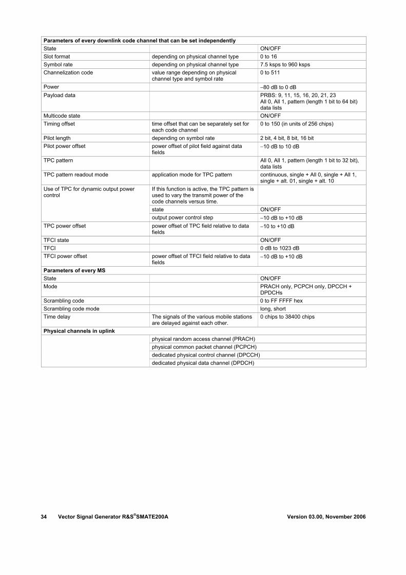
Parameters of every downlink code channel that can be set independently State ON/OFF Slot format depending on physical channel type 0 to 16 Symbol rate depending on physical channel type 7.5 ksps to 960 ksps Channelization code value range depending on physical
channel type and symbol rate 0 to 511
Power −80 dB to 0 dB Payload data PRBS: 9, 11, 15, 16, 20, 21, 23
All 0, All 1, pattern (length 1 bit to 64 bit) data lists
Multicode state ON/OFF Timing offset time offset that can be separately set for
each code channel 0 to 150 (in units of 256 chips)
Pilot length depending on symbol rate 2 bit, 4 bit, 8 bit, 16 bit Pilot power offset power offset of pilot field against data
fields −10 dB to 10 dB
TPC pattern All 0, All 1, pattern (length 1 bit to 32 bit), data lists
TPC pattern readout mode application mode for TPC pattern continuous, single + All 0, single + All 1, single + alt. 01, single + alt. 10
If this function is active, the TPC pattern is used to vary the transmit power of the code channels versus time.
state ON/OFF
Use of TPC for dynamic output power control
output power control step −10 dB to +10 dB TPC power offset power offset of TPC field relative to data
fields −10 to +10 dB
TFCI state ON/OFF TFCI 0 dB to 1023 dB TFCI power offset power offset of TFCI field relative to data
fields −10 dB to +10 dB
Parameters of every MS State ON/OFF Mode PRACH only, PCPCH only, DPCCH +
DPDCHs Scrambling code 0 to FF FFFF hex Scrambling code mode long, short Time delay The signals of the various mobile stations
are delayed against each other. 0 chips to 38400 chips
Physical channels in uplink physical random access channel (PRACH) physical common packet channel (PCPCH) dedicated physical control channel (DPCCH)
dedicated physical data channel (DPDCH)
Version 03.00, November 2006 Vector Signal Generator R&S®SMATE200A 35
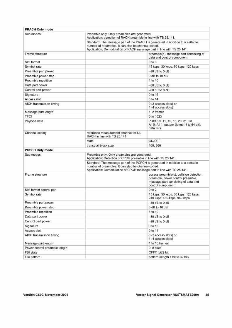
PRACH Only mode Preamble only: Only preambles are generated. Application: detection of RACH preamble in line with TS 25.141.
Sub modes
Standard: The message part of the PRACH is generated in addition to a settable number of preambles. It can also be channel-coded. Application: Demodulation of RACH message part in line with TS 25.141.
Frame structure preamble(s), message part consisting of data and control component
Slot format 0 to 3 Symbol rate 15 ksps, 30 ksps, 60 ksps, 120 ksps Preamble part power −80 dB to 0 dB Preamble power step 0 dB to 10 dB Preamble repetition 1 to 10 Data part power −80 dB to 0 dB Control part power −80 dB to 0 dB Signature 0 to 15 Access slot 0 to 14 AICH transmisson timing 0 (3 access slots) or
1 (4 access slots) Message part length 1, 2 frames TFCI 0 to 1023 Payload data PRBS: 9, 11, 15, 16, 20, 21, 23
All 0, All 1, pattern (length 1 to 64 bit), data lists
reference measurement channel for UL RACH in line with TS 25.141
state ON/OFF
Channel coding
transport block size 168, 360 PCPCH Only mode
Preamble only: Only preambles are generated. Application: Detection of CPCH preamble in line with TS 25.141.
Sub modes
Standard: The message part of the PCPCH is generated in addition to a settable number of preambles. It can also be channel-coded. Application: Demodulation of CPCH message part in line with TS 25.141.
Frame structure access preamble(s), collision detection preamble, power control preamble, message part consisting of data and control component
Slot format control part 0 to 2 Symbol rate 15 ksps, 30 ksps, 60 ksps, 120 ksps,
240 ksps, 480 ksps, 960 ksps Preamble part power −80 dB to 0 dB Preamble power step 0 dB to 10 dB Preamble repetition 1 to 10 Data part power −80 dB to 0 dB Control part power −80 dB to 0 dB Signature 0 to 15 Access slot 0 to 14 AICH transmisson timing 0 (3 access slots) or
1 (4 access slots) Message part length 1 to 10 frames Power control preamble length 0, 8 slots FBI state OFF/1 bit/2 bit FBI pattern pattern (length 1 bit to 32 bit)
Vector Signal Generator R&S®SMATE200A Version 03.00, November 2006 36
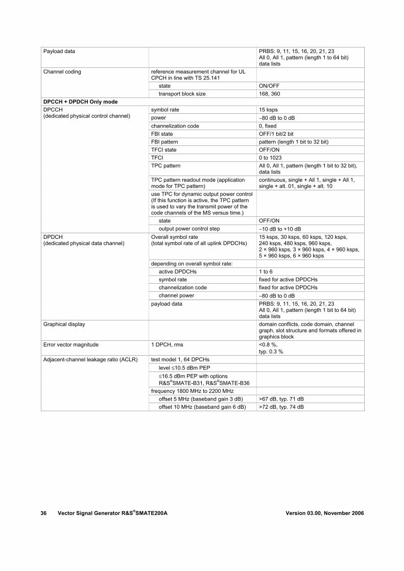
Payload data PRBS: 9, 11, 15, 16, 20, 21, 23 All 0, All 1, pattern (length 1 to 64 bit) data lists
reference measurement channel for UL CPCH in line with TS 25.141
state ON/OFF
Channel coding
transport block size 168, 360 DPCCH + DPDCH Only mode
symbol rate 15 ksps power −80 dB to 0 dB channelization code 0, fixed FBI state OFF/1 bit/2 bit FBI pattern pattern (length 1 bit to 32 bit) TFCI state OFF/ON TFCI 0 to 1023 TPC pattern All 0, All 1, pattern (length 1 bit to 32 bit),
data lists TPC pattern readout mode (application mode for TPC pattern)
continuous, single + All 1, single + All 1, single + alt. 01, single + alt. 10
use TPC for dynamic output power control(If this function is active, the TPC pattern is used to vary the transmit power of the code channels of the MS versus time.)
state OFF/ON
DPCCH (dedicated physical control channel)
output power control step −10 dB to +10 dB Overall symbol rate (total symbol rate of all uplink DPDCHs)
15 ksps, 30 ksps, 60 ksps, 120 ksps, 240 ksps, 480 ksps, 960 ksps, 2 × 960 ksps, 3 × 960 ksps, 4 × 960 ksps, 5 × 960 ksps, 6 × 960 ksps
depending on overall symbol rate: active DPDCHs 1 to 6 symbol rate fixed for active DPDCHs channelization code fixed for active DPDCHs channel power −80 dB to 0 dB
DPDCH (dedicated physical data channel)
payload data PRBS: 9, 11, 15, 16, 20, 21, 23 All 0, All 1, pattern (length 1 bit to 64 bit) data lists
Graphical display domain conflicts, code domain, channel graph, slot structure and formats offered in graphics block
Error vector magnitude 1 DPCH, rms <0.8 %, typ. 0.3 %
test model 1, 64 DPCHs level ≤10.5 dBm PEP ≤16.5 dBm PEP with options R&S®SMATE-B31, R&S®SMATE-B36
frequency 1800 MHz to 2200 MHz offset 5 MHz (baseband gain 3 dB) >67 dB, typ. 71 dB
Adjacent-channel leakage ratio (ACLR)
offset 10 MHz (baseband gain 6 dB) >72 dB, typ. 74 dB
Version 03.00, November 2006 Vector Signal Generator R&S®SMATE200A 37
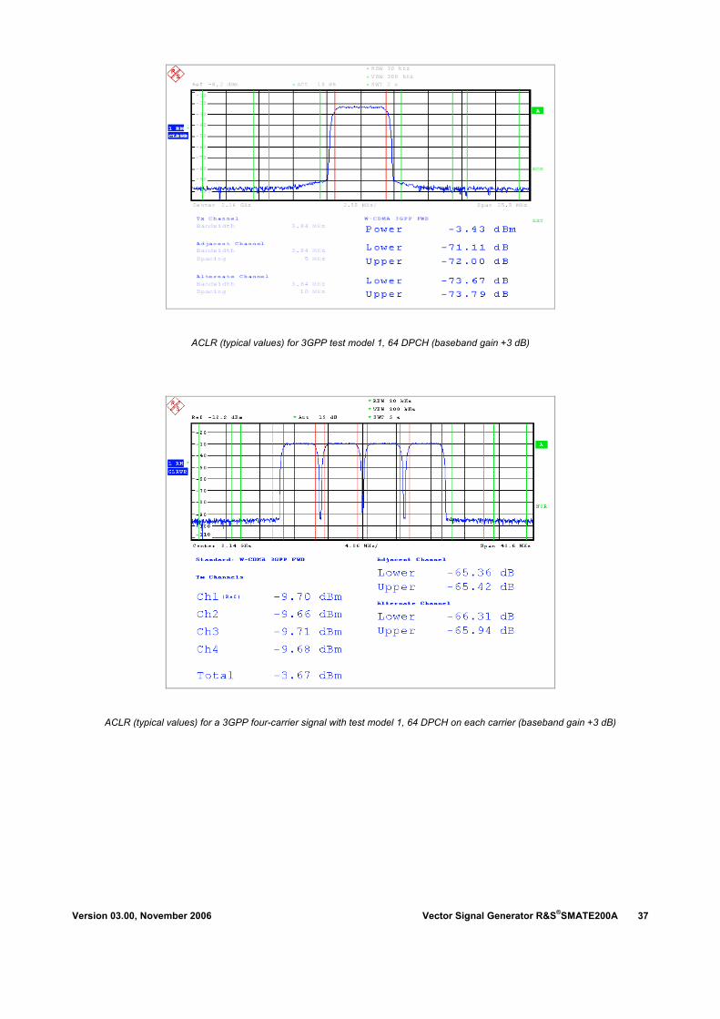
ACLR (typical values) for 3GPP test model 1, 64 DPCH (baseband gain +3 dB)
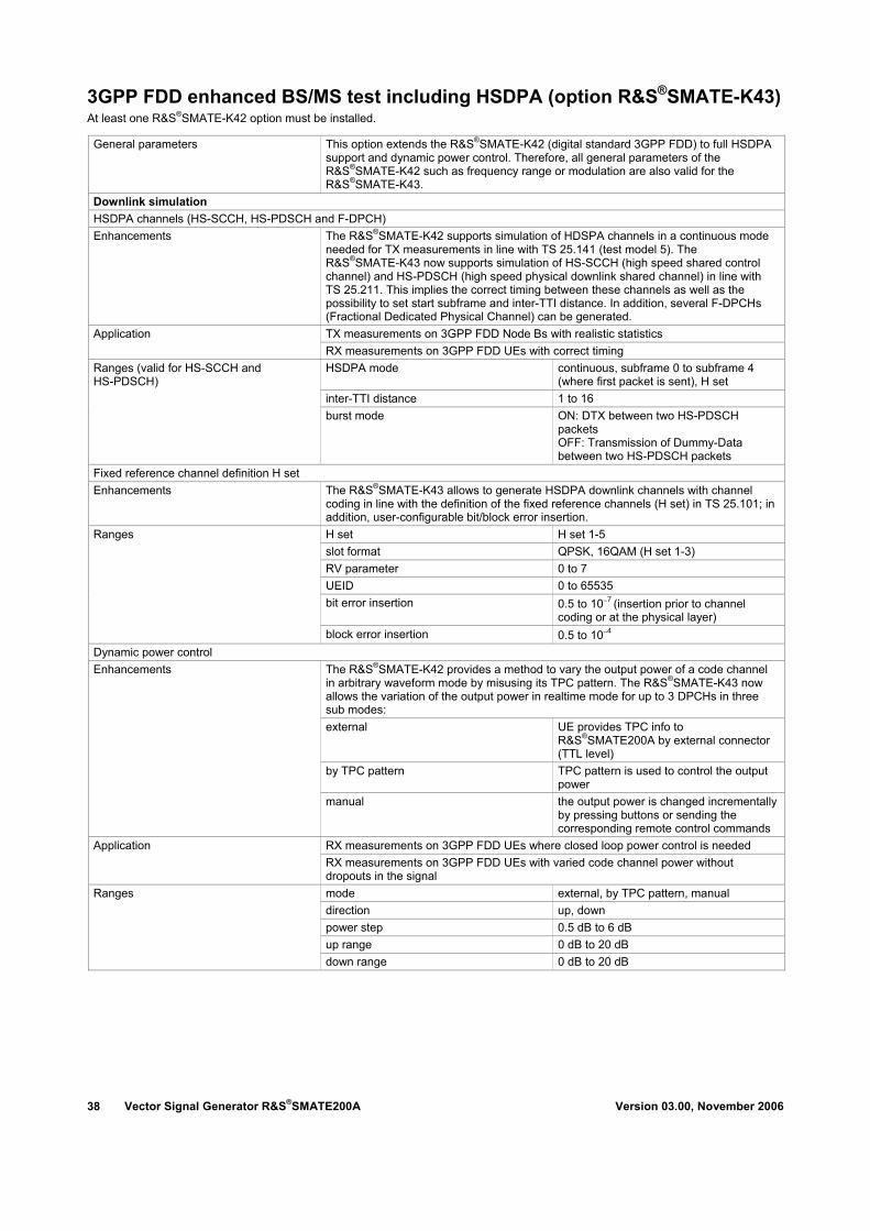
ACLR (typical values) for a 3GPP four-carrier signal with test model 1, 64 DPCH on each carrier (baseband gain +3 dB)
Vector Signal Generator R&S®SMATE200A Version 03.00, November 2006 38
3GPP FDD enhanced BS/MS test including HSDPA (option R&S®SMATE-K43) At least one R&S®SMATE-K42 option must be installed.
General parameters This option extends the R&S®SMATE-K42 (digital standard 3GPP FDD) to full HSDPA support and dynamic power control. Therefore, all general parameters of the R&S®SMATE-K42 such as frequency range or modulation are also valid for the R&S®SMATE-K43.
Downlink simulation HSDPA channels (HS-SCCH, HS-PDSCH and F-DPCH) Enhancements The R&S®SMATE-K42 supports simulation of HDSPA channels in a continuous mode
needed for TX measurements in line with TS 25.141 (test model 5). The R&S®SMATE-K43 now supports simulation of HS-SCCH (high speed shared control channel) and HS-PDSCH (high speed physical downlink shared channel) in line with TS 25.211. This implies the correct timing between these channels as well as the possibility to set start subframe and inter-TTI distance. In addition, several F-DPCHs (Fractional Dedicated Physical Channel) can be generated. TX measurements on 3GPP FDD Node Bs with realistic statistics Application RX measurements on 3GPP FDD UEs with correct timing HSDPA mode continuous, subframe 0 to subframe 4
(where first packet is sent), H set inter-TTI distance 1 to 16
Ranges (valid for HS-SCCH and HS-PDSCH)
burst mode ON: DTX between two HS-PDSCH packets OFF: Transmission of Dummy-Data between two HS-PDSCH packets
Fixed reference channel definition H set Enhancements The R&S®SMATE-K43 allows to generate HSDPA downlink channels with channel
coding in line with the definition of the fixed reference channels (H set) in TS 25.101; in addition, user-configurable bit/block error insertion. H set H set 1-5 slot format QPSK, 16QAM (H set 1-3) RV parameter 0 to 7 UEID 0 to 65535 bit error insertion 0.5 to 10−7 (insertion prior to channel
coding or at the physical layer)
Ranges
block error insertion 0.5 to 10−4 Dynamic power control
The R&S®SMATE-K42 provides a method to vary the output power of a code channel in arbitrary waveform mode by misusing its TPC pattern. The R&S®SMATE-K43 now allows the variation of the output power in realtime mode for up to 3 DPCHs in three sub modes: external UE provides TPC info to
R&S®SMATE200A by external connector (TTL level)
by TPC pattern TPC pattern is used to control the output power
Enhancements
manual the output power is changed incrementally by pressing buttons or sending the corresponding remote control commands
RX measurements on 3GPP FDD UEs where closed loop power control is needed Application RX measurements on 3GPP FDD UEs with varied code channel power without dropouts in the signal mode external, by TPC pattern, manual direction up, down power step 0.5 dB to 6 dB up range 0 dB to 20 dB
Ranges
down range 0 dB to 20 dB
Version 03.00, November 2006 Vector Signal Generator R&S®SMATE200A 39
Uplink simulation HS-DPCCH (high speed dedicated physical control channel) Enhancements The R&S®SMATE-K42 does not support HSDPA for uplink. The R&S®SMATE-K43 now
allows the simulation of a HS-DPCCH (high speed dedicated physical control channel) in realtime operation (UE1) and arbitrary waveform mode (UE2 to UE4). TX measurements on 3GPP FDD UEs supporting HSDPA Application RX measurements on 3GPP FDD Node Bs supporting HDSPA power −80 dB to 0 dB start delay 101 to 250 (in units of 256 chips) inter-TTI distance 1 subframe to 16 subframes CQI pattern up to 10 CQI values sent periodically,
support of DTX
Ranges
ACK/NACK pattern up to 32 ACK/NACK commands sent periodically, support of DTX
Dynamic power control The R&S®SMATE-K42 provides a method to vary the output power of a code channel in arbitrary waveform mode by misusing its TPC pattern. The R&S®SMATE-K43 now allows the variation of the output power in realtime mode for UE1 in three sub modes external node B provides TPC info to the
R&S®SMATE200A by external connector (TTL level)
by TPC pattern TPC pattern is used to control the output power
Enhancements
manual the output power is changed incrementally RX measurements on 3GPP FDD Node Bs where closed loop power control is needed Application RX measurements on 3GPP FDD Node Bs with varied UE power without dropouts in the signal mode external, by TPC pattern, manual direction up, down power step 0.5 dB to 6 dB up range 0 dB to 20 dB
Ranges
down range 0 dB to 20 dB
Vector Signal Generator R&S®SMATE200A Version 03.00, November 2006 40
Digital standard GPS (option R&S®SMATE-K44) Digital standard GPS to ICD-GPS-200 Revision C General settings Frequency default L1 = 1575.42 MHz
user-selectable in entire frequency range of R&S®SMATE200A
Output level default –115 dBm user-selectable in entire output level range of R&S®SMATE200A
Modulation BPSK (CDMA) Symbol rate (chip rate) 1.023 MHz Baseband filter Gaussian
filter parameter B × T = 1 generic mode Simulation modes localization mode navigation data bit (20460 chips) navigation data word (30 data bits) navigation data subframe (10 data words) navigation page (5 data subframes) complete navigation message (25 data pages) pulse pattern
Marker
ON/OFF ratio Triggering see I/Q baseband generator Navigation data identical for each satellite All 0
All 1 pattern (up to 64 bit) PN 9 to PN 23 data lists real navigation data
Real navigation data support of SEM-Almanac, arbitrary valid date and time (GMT)
Navigation data rate 50 bps Satellite configurations Number of channels 1 to 4 satellites Use spreading code identical for each satellite ON/OFF State separately settable for each satellite ON/OFF Space vehicle ID separately settable for each satellite C/A-codes: 37 Gold codes, 1023 chips
each Time shift separately settable for each satellite 0 to 10000000 (C/A-code-chip)/16 Power separately settable for each satellite ±10 dB Doppler shift separately settable for each satellite ±100 kHz (selectable in steps of 0.01 Hz) Localization mode Latitude latitude of simulated location ±90° (selectable in steps of 0.1 s) Longitude longitude of simulated location ±180° (selectable in steps of 0.1 s) Altitude altitude of simulated location ±10000 m
(selectable in steps of 0.1 m)
Version 03.00, November 2006 Vector Signal Generator R&S®SMATE200A 41
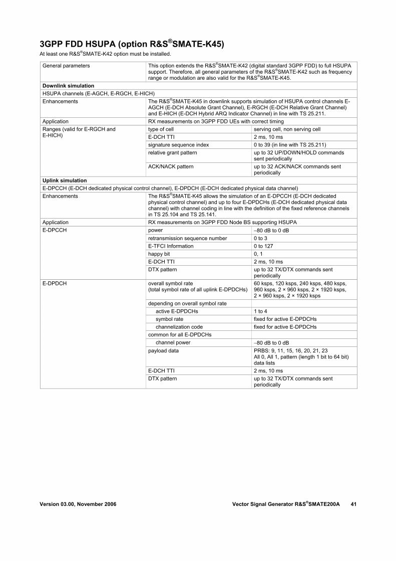
3GPP FDD HSUPA (option R&S®SMATE-K45) At least one R&S®SMATE-K42 option must be installed.
General parameters This option extends the R&S®SMATE-K42 (digital standard 3GPP FDD) to full HSUPA support. Therefore, all general parameters of the R&S®SMATE-K42 such as frequency range or modulation are also valid for the R&S®SMATE-K45.
Downlink simulation HSUPA channels (E-AGCH, E-RGCH, E-HICH) Enhancements The R&S®SMATE-K45 in downlink supports simulation of HSUPA control channels E-
AGCH (E-DCH Absolute Grant Channel), E-RGCH (E-DCH Relative Grant Channel) and E-HICH (E-DCH Hybrid ARQ Indicator Channel) in line with TS 25.211.
Application RX measurements on 3GPP FDD UEs with correct timing type of cell serving cell, non serving cell E-DCH TTI 2 ms, 10 ms signature sequence index 0 to 39 (in line with TS 25.211) relative grant pattern up to 32 UP/DOWN/HOLD commands
sent periodically
Ranges (valid for E-RGCH and E-HICH)
ACK/NACK pattern up to 32 ACK/NACK commands sent periodically
Uplink simulation E-DPCCH (E-DCH dedicated physical control channel), E-DPDCH (E-DCH dedicated physical data channel) Enhancements The R&S®SMATE-K45 allows the simulation of an E-DPCCH (E-DCH dedicated
physical control channel) and up to four E-DPDCHs (E-DCH dedicated physical data channel) with channel coding in line with the definition of the fixed reference channels in TS 25.104 and TS 25.141.
Application RX measurements on 3GPP FDD Node BS supporting HSUPA power −80 dB to 0 dB retransmission sequence number 0 to 3 E-TFCI Information 0 to 127 happy bit 0, 1 E-DCH TTI 2 ms, 10 ms
E-DPCCH
DTX pattern up to 32 TX/DTX commands sent periodically
overall symbol rate (total symbol rate of all uplink E-DPDCHs)
60 ksps, 120 ksps, 240 ksps, 480 ksps, 960 ksps, 2 × 960 ksps, 2 × 1920 ksps, 2 × 960 ksps, 2 × 1920 ksps
depending on overall symbol rate active E-DPDCHs 1 to 4 symbol rate fixed for active E-DPDCHs channelization code fixed for active E-DPDCHs
common for all E-DPDCHs channel power −80 dB to 0 dB
payload data PRBS: 9, 11, 15, 16, 20, 21, 23 All 0, All 1, pattern (length 1 bit to 64 bit) data lists
E-DCH TTI 2 ms, 10 ms
E-DPDCH
DTX pattern up to 32 TX/DTX commands sent periodically
Vector Signal Generator R&S®SMATE200A Version 03.00, November 2006 42
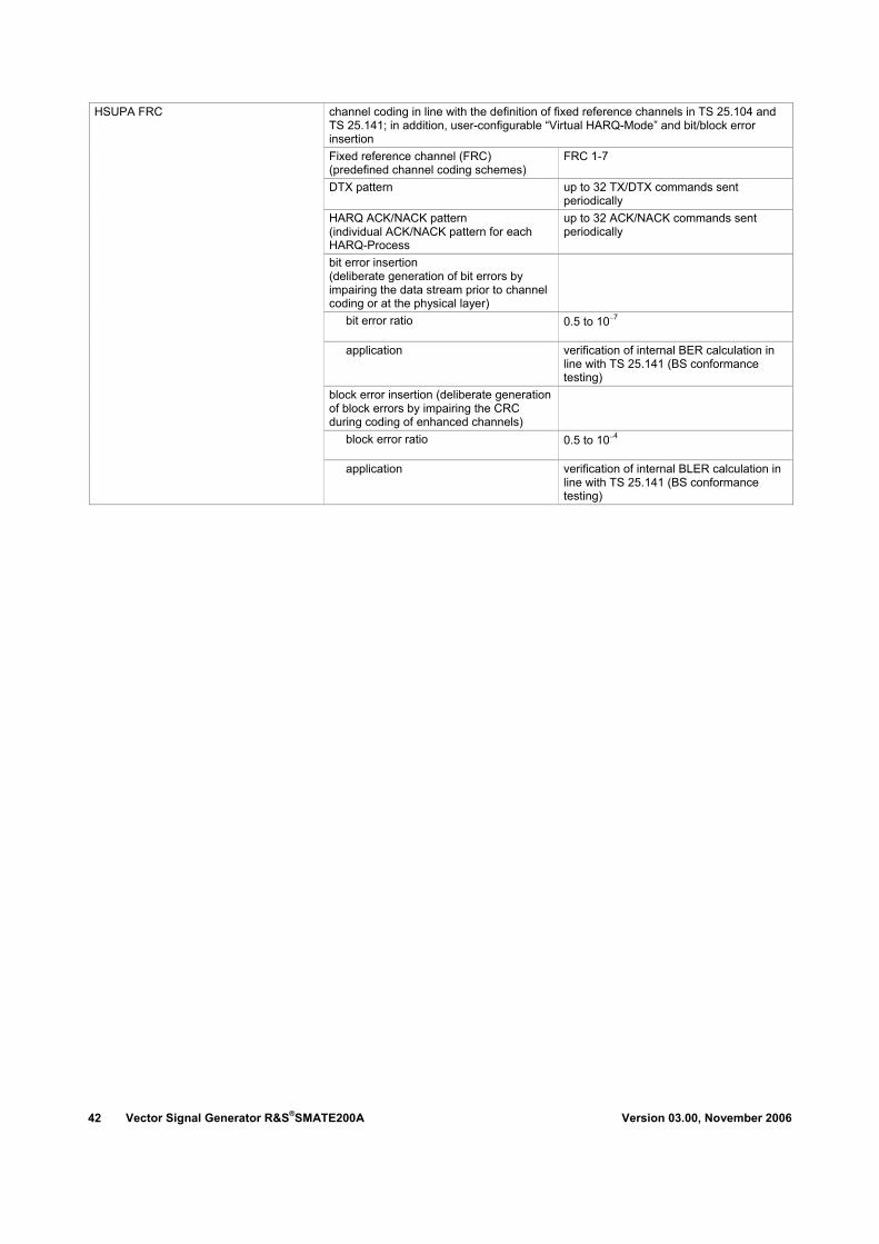
channel coding in line with the definition of fixed reference channels in TS 25.104 and TS 25.141; in addition, user-configurable “Virtual HARQ-Mode” and bit/block error insertion Fixed reference channel (FRC) (predefined channel coding schemes)
FRC 1-7
DTX pattern up to 32 TX/DTX commands sent periodically
HARQ ACK/NACK pattern (individual ACK/NACK pattern for each HARQ-Process
up to 32 ACK/NACK commands sent periodically
bit error insertion (deliberate generation of bit errors by impairing the data stream prior to channel coding or at the physical layer)
bit error ratio 0.5 to 10−7
application verification of internal BER calculation in line with TS 25.141 (BS conformance testing)
block error insertion (deliberate generation of block errors by impairing the CRC during coding of enhanced channels)
block error ratio 0.5 to 10−4
HSUPA FRC
application verification of internal BLER calculation in line with TS 25.141 (BS conformance testing)
Version 03.00, November 2006 Vector Signal Generator R&S®SMATE200A 43
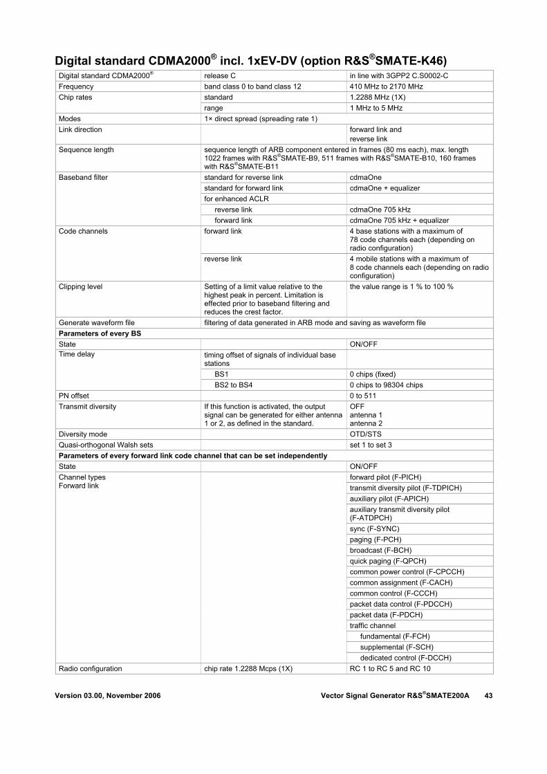
Digital standard CDMA2000® incl. 1xEV-DV (option R&S®SMATE-K46) Digital standard CDMA2000® release C in line with 3GPP2 C.S0002-C Frequency band class 0 to band class 12 410 MHz to 2170 MHz
standard 1.2288 MHz (1X) Chip rates range 1 MHz to 5 MHz
Modes 1× direct spread (spreading rate 1) Link direction forward link and
reverse link Sequence length sequence length of ARB component entered in frames (80 ms each), max. length
1022 frames with R&S®SMATE-B9, 511 frames with R&S®SMATE-B10, 160 frames with R&S®SMATE-B11 standard for reverse link cdmaOne standard for forward link cdmaOne + equalizer for enhanced ACLR
reverse link cdmaOne 705 kHz
Baseband filter
forward link cdmaOne 705 kHz + equalizer forward link 4 base stations with a maximum of
78 code channels each (depending on radio configuration)
Code channels
reverse link 4 mobile stations with a maximum of 8 code channels each (depending on radio configuration)
Clipping level Setting of a limit value relative to the highest peak in percent. Limitation is effected prior to baseband filtering and reduces the crest factor.
the value range is 1 % to 100 %
Generate waveform file filtering of data generated in ARB mode and saving as waveform file Parameters of every BS State ON/OFF
timing offset of signals of individual base stations
BS1 0 chips (fixed)
Time delay
BS2 to BS4 0 chips to 98304 chips PN offset 0 to 511 Transmit diversity If this function is activated, the output
signal can be generated for either antenna 1 or 2, as defined in the standard.
OFF antenna 1 antenna 2
Diversity mode OTD/STS Quasi-orthogonal Walsh sets set 1 to set 3 Parameters of every forward link code channel that can be set independently State ON/OFF
forward pilot (F-PICH) transmit diversity pilot (F-TDPICH) auxiliary pilot (F-APICH) auxiliary transmit diversity pilot (F-ATDPCH) sync (F-SYNC) paging (F-PCH) broadcast (F-BCH) quick paging (F-QPCH) common power control (F-CPCCH) common assignment (F-CACH) common control (F-CCCH) packet data control (F-PDCCH) packet data (F-PDCH) traffic channel
fundamental (F-FCH) supplemental (F-SCH)
Channel types Forward link
dedicated control (F-DCCH) Radio configuration chip rate 1.2288 Mcps (1X) RC 1 to RC 5 and RC 10
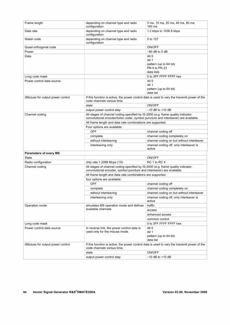
Vector Signal Generator R&S®SMATE200A Version 03.00, November 2006 44
Frame length depending on channel type and radio configuration
5 ms, 10 ms, 20 ms, 40 ms, 80 ms, 160 ms
Data rate depending on channel type and radio configuration
1.2 kbps to 1036.8 kbps
Walsh code depending on channel type and radio configuration
0 to 127
Quasi-orthogonal code ON/OFF Power –80 dB to 0 dB Data All 0
All 1 pattern (up to 64 bit) PN 9 to PN 23 data lists
Long code mask 0 to 3FF FFFF FFFF hex Power control data source All 0
All 1 pattern (up to 64 bit) data list
If this function is active, the power control data is used to vary the transmit power of the code channels versus time. state ON/OFF
(Mis)use for output power control
output power control step –10 dB to +10 dB All stages of channel coding specified by IS-2000 (e.g. frame quality indicator, convolutional encoder/turbo coder, symbol puncture and interleaver) are available. All frame length and data rate combinations are supported. Four options are available:
OFF channel coding off complete channel coding completely on without interleaving channel coding on but without interleaver
Channel coding
interleaving only channel coding off, only interleaver is active
Parameters of every MS State ON/OFF Radio configuration chip rate 1.2288 Mcps (1X) RC 1 to RC 4
All stages of channel coding specified by IS-2000 (e.g. frame quality indicator, convolutional encoder, symbol puncture and interleaver) are available. All frame length and data rate combinations are supported. four options are available:
OFF channel coding off complete channel coding completely on without interleaving channel coding on but without interleaver
Channel coding
interleaving only channel coding off, only interleaver is active traffic access enhanced access
Operation mode simulates MS operation mode and defines available channels
common control Long code mask 0 to 3FF FFFF FFFF hex Power control data source In reverse link, the power control data is
used only for the misuse mode. All 0 All 1 pattern (up to 64 bit) data list
If this function is active, the power control data is used to vary the transmit power of the code channels versus time. state ON/OFF
(Mis)use for output power control
output power control step –10 dB to +10 dB
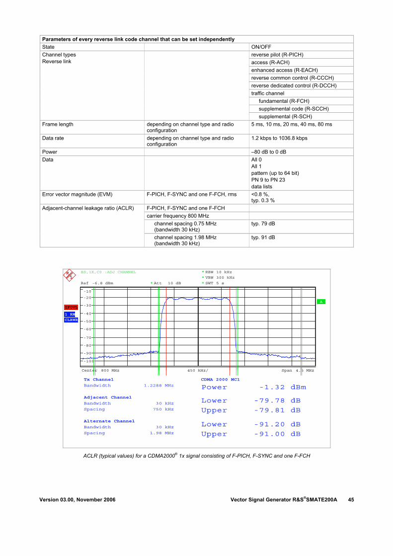
Version 03.00, November 2006 Vector Signal Generator R&S®SMATE200A 45
Parameters of every reverse link code channel that can be set independently State ON/OFF
reverse pilot (R-PICH) access (R-ACH) enhanced access (R-EACH) reverse common control (R-CCCH) reverse dedicated control (R-DCCH) traffic channel
fundamental (R-FCH) supplemental code (R-SCCH)
Channel types Reverse link
supplemental (R-SCH) Frame length depending on channel type and radio
configuration 5 ms, 10 ms, 20 ms, 40 ms, 80 ms
Data rate depending on channel type and radio configuration
1.2 kbps to 1036.8 kbps
Power –80 dB to 0 dB Data All 0
All 1 pattern (up to 64 bit) PN 9 to PN 23 data lists
Error vector magnitude (EVM) F-PICH, F-SYNC and one F-FCH, rms <0.8 %, typ. 0.3 %
F-PICH, F-SYNC and one F-FCH carrier frequency 800 MHz
channel spacing 0.75 MHz (bandwidth 30 kHz)
typ. 79 dB
Adjacent-channel leakage ratio (ACLR)
channel spacing 1.98 MHz (bandwidth 30 kHz)
typ. 91 dB
A
Ref -6.8 dBm
CLRWR
BS,1X,C0 :ADJ CHANNEL
1 RM
Att 10 dB*
*
*
RBW 10 kHz
VBW 300 kHz
SWT 5 s*
Center 800 MHz Span 4.5 MHz450 kHz/
IFOVL
-100
-90
-80
-70
-60
-50
-40
-30
-20
-10
Tx Channel CDMA 2000 MC1
Bandwidth 1.2288 MHz Power -1.32 dBm
Adjacent Channel
Bandwidth 30 kHz Lower -79.78 dB Spacing 750 kHz Upper -79.81 dB
Alternate Channel
Bandwidth 30 kHz Lower -91.20 dB Spacing 1.98 MHz Upper -91.00 dB
ACLR (typical values) for a CDMA2000® 1x signal consisting of F-PICH, F-SYNC and one F-FCH
Vector Signal Generator R&S®SMATE200A Version 03.00, November 2006 46
Digital standard IEEE 802.11 a/b/g (option R&S®SMATE-K48) Digital standard IEEE 802.11 a/b/g in line with IEEE 802.11a-1999,
IEEE 802.11b-1999, IEEE 802.11g-2003 General settings
unframed generation of a non-packet-oriented signal without frame structure, with the modulation modes and data rates defined by the IEEE 802.11 standard
Modes
framed generation of a sequence of data packets with the frame structure defined by the standard, interrupted by an idle time
Sequence length 1 to 511 frames (depending on frame duration)
Clipping vector or scalar clipping, applied before filtering
Marker modes restart, frame start, frame active part, pulse, pattern, on/off ratio
Triggering see I/Q baseband generator Parameters in framed mode
time between two successive packets (PPDUs)
Idle time
range 0 s to 10000 µs MAC header activating and configuring the MAC header
with the parameters frame control, duration/ID, address 1 to 4 and sequence control
Frame check sequence activating or deactivating a 32 bit (4 byte) check sum for protecting the MAC header and the user data (frame body)
Settings for CCK (IEEE 802.11b/IEEE 802.11g) standard 11 Mcps Chip rate range as R&S®SMATE200A
Baseband filter spectral mask in line with IEEE 802.11b-1999 – Wireless LAN MAC and PHY specifications – chapter 18.4.7.3
PLCP preamble and header format long PLCP and short PLCP PSDU bit rate 1 Mbps, 2 Mbps, 5.5 Mbps, 11 Mbps PSDU modulation (depending on PSDU bit rate)
DBPSK, DQPSK, CCK
PSDU data length (length of user data field in bytes of the packet to be transferred
range 0 byte to 4095 byte
Parameters in framed mode
scrambling data scrambling can be activated or deactivated
PSDU bit rate 1 Mbps, 2 Mbps, 5.5 Mbps or 11 Mbps PSDU modulation (depending on PSDU bit rate)
DBPSK, DQPSK, CCK Parameters in unframed mode
scrambling data scrambling can be activated or deactivated
Settings for OFDM (IEEE 802.11a/IEEE 802.11g) standard 20 Msample/s Kernel sample rate range as R&S®SMATE200A
Baseband filter spectral mask in line with IEEE 802.11b-1999 – Wireless LAN MAC and PHY specifications – chapter 17.3.9.6.2

Version 03.00, November 2006 Vector Signal Generator R&S®SMATE200A 47
PLCP preamble and header format long PLCP and short PLCP PLCP signal field automatically calculated PSDU bit rate 6 Mbps, 9 Mbps, 12 Mbps, 18 Mbps,
24 Mbps, 36 Mbps, 48 Mbps or 54 Mbps PSDU modulation (depending on PSDU bit rate)
BPSK, QPSK, 16QAM, 64QAM
PSDU data length (length of user data field in bytes of the packet to be transferred
range 0 byte to 4095 byte number of data symbols (number of OFDM symbols in data portion of packet)
directly proportional to PSDU data length
scrambling data scrambling can be activated or deactivated; initial scrambler state can be set randomly or to a user-defined value
interleaver can be activated or deactivated time domain windowing (transition times) 0 s to 1000 ns
Parameters in framed mode
service field user-defined service field value supported PSDU bit rate 6 Mbps, 9 Mbps, 12 Mbps, 18 Mbps,
24 Mbps, 36 Mbps, 48 Mbps or 54 Mbps PSDU modulation (depending on PSDU bit rate)
BPSK, QPSK, 16QAM, 64QAM
PSDU data length (length of user data field in bytes of the packet to be transferred
range 0 byte to 2312 byte number of data symbols (number of OFDM symbols to be generated)
directly proportional to PSDU data length
scrambling data scrambling can be activated or deactivated; initial scrambler state can be set randomly or to a user-defined value
interleaver can be activated or deactivated time domain windowing (transition times) 0 s to 1000 ns
Parameters in unframed mode
service field user-defined service field value supported Settings for PBCC (IEEE 802.11b/IEEE 802.11g)
standard 11 Mcps Chip rate range as R&S®SMATE200A
Baseband filter spectral mask in line with IEEE 802.11b-1999-Wireless LAN MAC and PHY specifications – chapter 18.4.7.3
PLCP preamble and header format long PLCP and short PLCP PSDU bit rate 1 Mbps, 2 Mbps, 5.5 Mbps, 11 Mbps,
22 Mbps PSDU modulation (depending on PSDU bit rate)
DBPSK, DQPSK, PBCC
PSDU data length (length of user data field in bytes of the packet to be transferred)
range 0 byte to 4095 byte
Parameters in framed modes
scrambling data scrambling can be activated or deactivated
PSDU bit rate 1 Mbps, 2 Mbps, 5.5 Mbps, 11 Mbps, 22 Mbps
PSDU modulation (depending on PSDU bit rate)
DBPSK, DQPSK, PBCC
Parameters in unframed mode
scrambling data scrambling can be activated or deactivated
Vector Signal Generator R&S®SMATE200A Version 03.00, November 2006 48
Digital standard IEEE 802.16 WiMAX including IEEE 802.16e (option R&S®SMATE-K49) Digital standard IEEE 802.16 in line with IEEE 802.16 – 2004/Cor1/D5
and IEEE 802.16e-2005 Link direction forward link and
reverse link Physical layer modes OFDM, OFDMA, OFDMA – WiBro Duplexing TDD, FDD Frame durations 2 ms, 2.5 ms, 4 ms, 5 ms, 8 ms, 10 ms,
12.5 ms, 20 ms, continuous, user Sequence length (frames) depending on frame duration, sample rate
and available ARB memory 1 to >2000
Predefined frames in OFDM mode short, mid and long test messages for BPSK, QPSK, 16QAM and 64QAM modulation
in OFDM mode FCH/burst or preamble Level reference in OFDMA/WiBro mode preamble or subframe RMS power
Parameters in OFDM mode Predefined frequency bands ETSI, MMDS, WCS, U-NII, user Channel bandwidth depending on selected frequency band 1.25 MHz to 30 MHz Sampling rate depending on channel bandwidth 1.5 MHz to 32 MHz Tg/Tb settings 1/4, 1/8, 1/16, 1/32 FFT size 256 (fixed) Frame preamble long, short, off Modulation and RS-CC rates BPSK 1/2, QPSK 1/2, QPSK 3/4,
16QAM 1/2, 16QAM 3/4, 64QAM 2/3, 64QAM 3/4
Subchannelization (number of possible channels)
1, 2, 4, 8, 16 (all)
No. of bursts with different modulation formats per frame
64
Burst types data, DL-MAP, UL-MAP, ranging Data All 0
All 1 pattern (up to 64 bit) PN 9 to PN 23 data lists
Midamble repetition in uplink mode off, 5, 9, 17 Parameters in OFDMA Mode Predefined frequency bands ETSI, MMDS, WCS, U-NII, WiBro, user Channel bandwidth depending on selected frequency band 1.25 MHz to 30 MHz Sampling rate depending on channel bandwidth 1.5 MHz to 32 MHz Tg/Tb settings 1/4, 1/8, 1/16, 1/32 FFT size 128, 512, 1024, 2048 Preamble modes Auto and User with index 0 to 113 Number of zones/segments 8 Space-time coding modes OFF
2 antennas matrix A 2 antennas matrix B
Modulation and coding rates QPSK 1/2, QPSK 3/4, 16QAM 1/2, 16QAM 3/4, 64QAM 1/2, 64QAM 2/3, 64QAM 3/4
Channel coding modes off, CC, CTC Channel coding parts scrambler, FEC, interleaver can be
switched on/off independently Repetition coding 0, 2, 4, 6
Version 03.00, November 2006 Vector Signal Generator R&S®SMATE200A 49
Subcarrier permutation FUSC, PUSC Subchannel map user definable for PUSC Number of bursts with different modulation formats
64
Burst types FCH, DL-MAP, UL-MAP, ranging, data Data All 0
All 1 pattern (up to 64 bit) PN 9 to PN 23 data lists
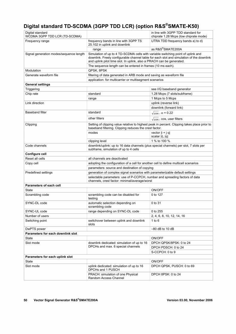
Vector Signal Generator R&S®SMATE200A Version 03.00, November 2006 50
Digital standard TD-SCDMA (3GPP TDD LCR) (option R&S®SMATE-K50) Digital standard WCDMA 3GPP TDD LCR (TD-SCDMA)
in line with 3GPP TDD standard for chiprate 1.28 Mcps (low chiprate mode)
frequency bands in line with 3GPP TS 25.102 in uplink and downlink
UTRA TDD frequency bands a) to d) Frequency range
range as R&S®SMATE200A Simulation of up to 4 TD-SCDMA cells with variable switching point of uplink and downlink. Freely configurable channel table for each slot and simulation of the downlink and uplink pilot time slot. In uplink, also a PRACH can be generated.
Signal generation modes/sequence length
The sequence length can be entered in frames (10 ms each). Modulation QPSK, 8PSK
filtering of data generated in ARB mode and saving as waveform file Generate waveform file application: for multicarrier or multisegment scenarios
General settings Triggering see I/Q baseband generator
standard 1.28 Mcps (7 slots/subframe) Chip rate range 1 Mcps to 5 Mcps
uplink (reverse link) Link direction downlink (forward link)
standard cos , α = 0.22 Baseband filter
other filters cos , cos, user filters
Setting of clipping value relative to highest peak in percent. Clipping takes place prior to baseband filtering. Clipping reduces the crest factor. modes vector |i + j q|
scalar |i|, |q|
Clipping
clipping level 1 % to 100 % Code channels downlink/uplink: up to 16 data channels (plus special channels) per slot, 7 slots per
subframe, simulation of up to 4 cells Configure cell Reset all cells all channels are deactivated
adopting the configuration of a cell for another cell to define multicell scenarios Copy cell parameters: source and destination of copying generation of complex signal scenarios with parameterizable default settings Predefined settings selectable parameters: use of P-CCPCH, number and spreading factors of data channels, crest factor: minimal/average/worst
Parameters of each cell State ON/OFF Scrambling code scrambling code can be disabled for
testing 0 to 127
SYNC-DL code automatic selection depending on scrambling code
0 to 31
SYNC-UL code range depending on SYNC-DL code 0 to 255 Number of users 2, 4, 6, 8, 10, 12, 14, 16 Switching point switchover between uplink and downlink
slots 1 to 6
DwPTS power –80 dB to 10 dB Parameters for each downlink slot State ON/OFF
DPCH QPSK/8PSK: 0 to 24 DPCH PDSCH: 0 to 24
Slot mode downlink dedicated: simulation of up to 16 DPCHs and max. 6 special channels
S-CCPCH: 0 to 9 Parameters for each uplink slot State ON/OFF
uplink dedicated: simulation of up to 16 DPCHs and 1 PUSCH
DPCH QPSK, PUSCH: 0 to 69 Slot mode
PRACH: simulation of one Physical Random Access Channel
DPCH 8PSK: 0 to 24
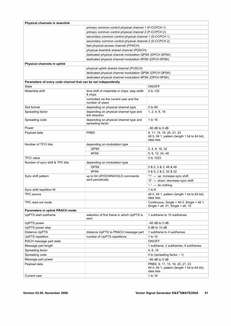
Version 03.00, November 2006 Vector Signal Generator R&S®SMATE200A 51
Physical channels in downlink primary common control physical channel 1 (P-CCPCH 1) primary common control physical channel 2 (P-CCPCH 2) secondary common control physical channel 1 (S-CCPCH 1) secondary common control physical channel 2 (S-CCPCH 2) fast physical access channel (FPACH) physical downlink shared channel (PDSCH) dedicated physical channel modulation QPSK (DPCH QPSK)
dedicated physical channel modulation 8PSK (DPCH 8PSK) Physical channels in uplink
physical uplink shared channel (PUSCH) dedicated physical channel modulation QPSK (DPCH QPSK)
dedicated physical channel modulation 8PSK (DPCH 8PSK) Parameters of every code channel that can be set independently State ON/OFF
time shift of midamble in chips: step width 8 chips
0 to 120 Midamble shift
controlled via the current user and the number of users
Slot format depending on physical channel type 0 to 69 Spreading factor depending on physical channel type and
link direction 1, 2, 4, 8, 16
Spreading code depending on physical channel type and spreading factor
1 to 16
Power −80 dB to 0 dB Payload data PRBS 9, 11, 15, 16, 20, 21, 23
All 0, All 1, pattern (length 1 bit to 64 bit), data lists
depending on modulation type QPSK 0, 4, 8, 16, 32
Number of TFCI bits
8PSK 0, 6, 12, 24, 48 TFCI value 0 to 1023
depending on modulation type QPSK 0 & 0, 3 & 3, 48 & 48
Number of sync shift & TPC bits
8PSK 0 & 0, 2 & 2, 32 & 32 “1” → up: increase sync shift “0” → down: decrease sync shift
Sync shift pattern up to 64 UP/DOWN/HOLD commands sent periodically
“–“ → do nothing Sync shift repetition M 1 to 8 TPC source All 0, All 1, pattern (length 1 bit to 64 bit),
data lists TPC read out mode Continuous, Single + All 0, Single + All 1,
Single + alt. 01, Single + alt. 10 Parameters in uplink PRACH mode UpPTS start subframe selection of first frame in which UpPTS is
sent 1 subframe to 10 subframes
UpPTS power –80 dB to 0 dB UpPTS power step 0 dB to 10 dB Distance UpPTS distance UpPTS to PRACH message part 1 subframe to 4 subframes UpPTS repetition number of UpPTS repetitions 1 to 10 RACH message part state ON/OFF Message part length 1 subframe, 2 subframes, 4 subframes Spreading factor 4, 8, 16 Spreading code 0 to (spreading factor – 1) Message part power −80 dB to 0 dB Payload data PRBS: 9, 11, 15, 16, 20, 21, 23
All 0, All 1, pattern (length 1 bit to 64 bit), data lists
Current user 1 to 16
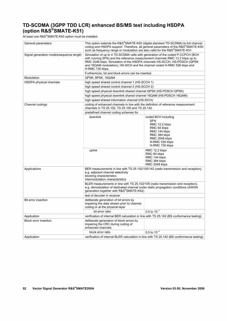
Vector Signal Generator R&S®SMATE200A Version 03.00, November 2006 52
TD-SCDMA (3GPP TDD LCR) enhanced BS/MS test including HSDPA (option R&S®SMATE-K51) At least one R&S®SMATE-K50 option must be installed.
General parameters This option extends the R&S®SMATE-K50 (digital standard TD-SCDMA) to full channel coding and HSDPA support. Therefore, all general parameters of the R&S®SMATE-K50 such as frequency range or modulation are also valid for the R&S®SMATE-K51. Simulation of up to 4 TD-SCDMA cells with generation of the coded P-CCPCH (BCH with running SFN) and the reference measurement channels RMC 12.2 kbps up to RMC 2048 kbps. Simulation of the HSDPA channels HS-SCCH, HS-PDSCH (QPSK and 16QAM modulation), HS-SICH and the channel coded H-RMC 526 kbps and H-RMC 730 kbps.
Signal generation modes/sequence length
Furthermore, bit and block errors can be inserted. Modulation QPSK, 8PSK, 16QAM
high speed shared control channel 1 (HS-SCCH 1) high speed shared control channel 2 (HS-SCCH 2) high speed physical downlink shared channel QPSK (HS-PDSCH QPSK) high speed physical downlink shared channel 16QAM (HS-PDSCH 16QAM)
HSDPA physical channels
high speed shared information channel (HS-SICH) coding of enhanced channels in line with the definition of reference measurement channels in TS 25.102, TS 25.105 and TS 25.142 predefined channel coding schemes for
downlink coded BCH including SFN RMC 12.2 kbps RMC 64 kbps RMC 144 kbps RMC 384 kbps RMC 2048 kbps H-RMC 526 kbps H-RMC 730 kbps
Channel codings
uplink RMC 12.2 kbps RMC 64 kbps RMC 144 kbps RMC 384 kbps RMC 2048 kbps
BER measurements in line with TS 25.102/105/142 (radio transmission and reception), e.g. adjacent channel selectivity blocking characteristics intermodulation characteristics BLER measurements in line with TS 25.102/105 (radio transmission and reception), e.g. demodulation of dedicated channel under static propagation conditions (AWGN generation together with R&S®SMATE-K62)
Applications
test of decoder in receiver deliberate generation of bit errors by impairing the data stream prior to channel coding or at the physical layer
Bit error insertion
bit error ratio 0.5 to 10−7 Application verification of internal BER calculation in line with TS 25.142 (BS conformance testing)
deliberate generation of block errors by impairing the CRC during coding of enhanced channels
Block error insertion
block error ratio 0.5 to 10−4 Application verification of internal BLER calculation in line with TS 25.142 (BS conformance testing)
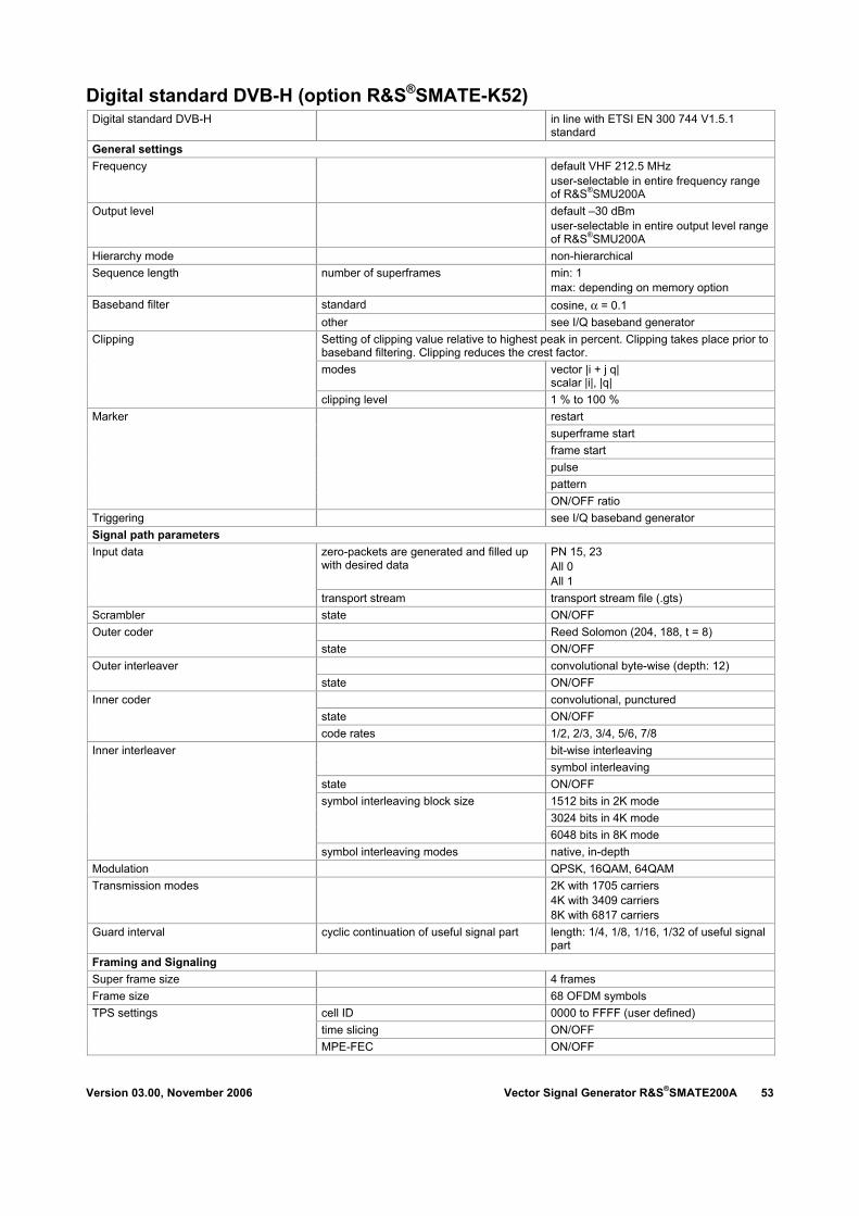
Version 03.00, November 2006 Vector Signal Generator R&S®SMATE200A 53
Digital standard DVB-H (option R&S®SMATE-K52) Digital standard DVB-H in line with ETSI EN 300 744 V1.5.1
standard General settings Frequency default VHF 212.5 MHz
user-selectable in entire frequency range of R&S®SMU200A
Output level default –30 dBm user-selectable in entire output level range of R&S®SMU200A
Hierarchy mode non-hierarchical Sequence length number of superframes min: 1
max: depending on memory option standard cosine, α = 0.1 Baseband filter other see I/Q baseband generator Setting of clipping value relative to highest peak in percent. Clipping takes place prior to baseband filtering. Clipping reduces the crest factor. modes vector |i + j q|
scalar |i|, |q|
Clipping
clipping level 1 % to 100 % restart superframe start frame start pulse pattern
Marker
ON/OFF ratio Triggering see I/Q baseband generator Signal path parameters
zero-packets are generated and filled up with desired data
PN 15, 23 All 0 All 1
Input data
transport stream transport stream file (.gts) Scrambler state ON/OFF
Reed Solomon (204, 188, t = 8) Outer coder state ON/OFF convolutional byte-wise (depth: 12) Outer interleaver state ON/OFF convolutional, punctured state ON/OFF
Inner coder
code rates 1/2, 2/3, 3/4, 5/6, 7/8 bit-wise interleaving symbol interleaving
state ON/OFF 1512 bits in 2K mode 3024 bits in 4K mode
symbol interleaving block size
6048 bits in 8K mode
Inner interleaver
symbol interleaving modes native, in-depth Modulation QPSK, 16QAM, 64QAM Transmission modes 2K with 1705 carriers
4K with 3409 carriers 8K with 6817 carriers
Guard interval cyclic continuation of useful signal part length: 1/4, 1/8, 1/16, 1/32 of useful signal part
Framing and Signaling Super frame size 4 frames Frame size 68 OFDM symbols
cell ID 0000 to FFFF (user defined) time slicing ON/OFF
TPS settings
MPE-FEC ON/OFF
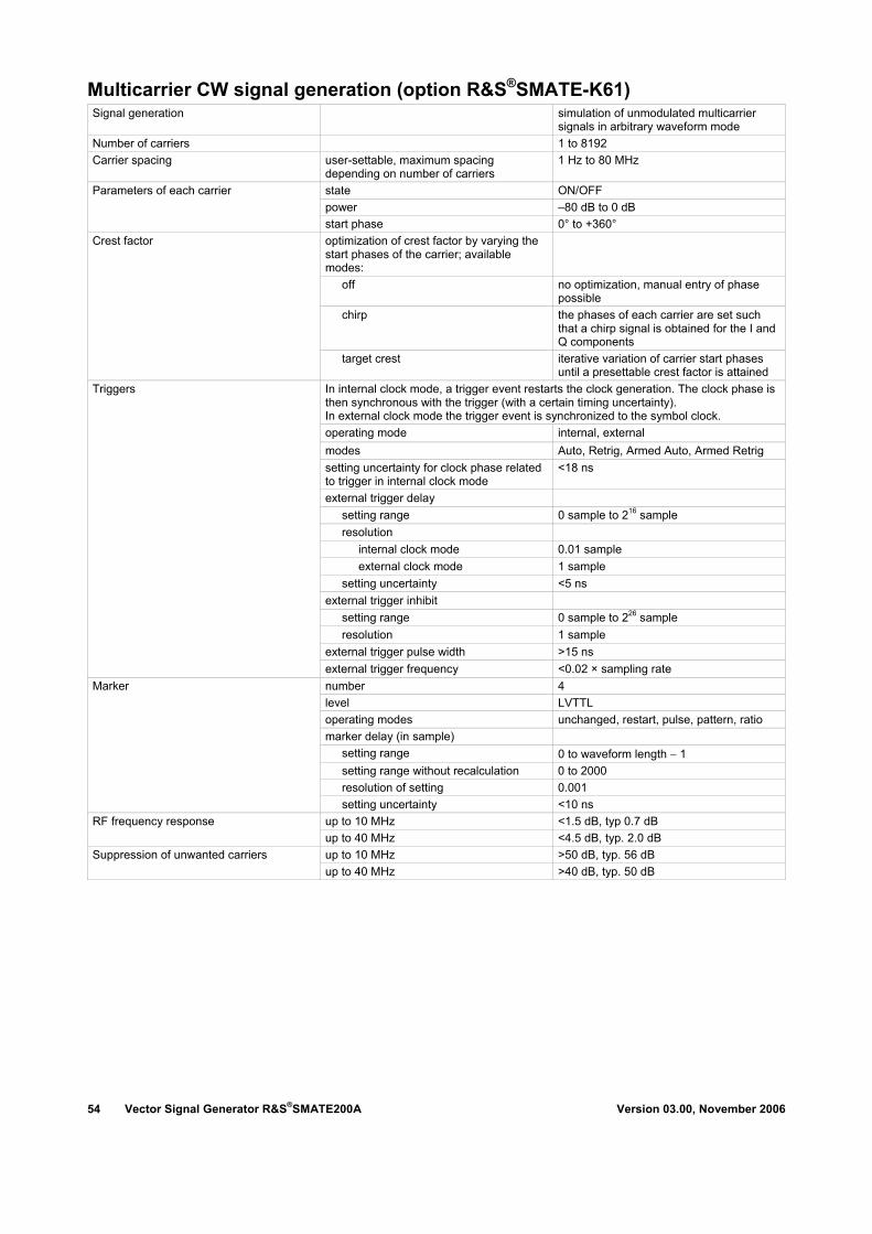
Vector Signal Generator R&S®SMATE200A Version 03.00, November 2006 54
Multicarrier CW signal generation (option R&S®SMATE-K61) Signal generation simulation of unmodulated multicarrier
signals in arbitrary waveform mode Number of carriers 1 to 8192 Carrier spacing user-settable, maximum spacing
depending on number of carriers 1 Hz to 80 MHz
state ON/OFF power –80 dB to 0 dB
Parameters of each carrier
start phase 0° to +360° optimization of crest factor by varying the start phases of the carrier; available modes:
off no optimization, manual entry of phase possible
chirp the phases of each carrier are set such that a chirp signal is obtained for the I and Q components
Crest factor
target crest iterative variation of carrier start phases until a presettable crest factor is attained
In internal clock mode, a trigger event restarts the clock generation. The clock phase is then synchronous with the trigger (with a certain timing uncertainty). In external clock mode the trigger event is synchronized to the symbol clock. operating mode internal, external modes Auto, Retrig, Armed Auto, Armed Retrig setting uncertainty for clock phase related to trigger in internal clock mode
<18 ns
external trigger delay setting range 0 sample to 216 sample resolution
internal clock mode 0.01 sample external clock mode 1 sample
setting uncertainty <5 ns external trigger inhibit
setting range 0 sample to 226 sample resolution 1 sample
external trigger pulse width >15 ns
Triggers
external trigger frequency <0.02 × sampling rate number 4 level LVTTL operating modes unchanged, restart, pulse, pattern, ratio marker delay (in sample)
setting range 0 to waveform length − 1 setting range without recalculation 0 to 2000 resolution of setting 0.001
Marker
setting uncertainty <10 ns up to 10 MHz <1.5 dB, typ 0.7 dB RF frequency response up to 40 MHz <4.5 dB, typ. 2.0 dB up to 10 MHz >50 dB, typ. 56 dB Suppression of unwanted carriers up to 40 MHz >40 dB, typ. 50 dB
Version 03.00, November 2006 Vector Signal Generator R&S®SMATE200A 55
Spectrum of multicarrier CW
Vector Signal Generator R&S®SMATE200A Version 03.00, November 2006 56
Digital standards with R&S®WinIQSIM™ (for R&S®SMATE-B9/-B10/-B11 ARB)
Digital standard IS-95 (option R&S®SMATE-K11) Digital standard CDMA2000® (option R&S®SMATE-K12) Digital standard 3GPP TDD HDR (option R&S®SMATE-K13) Digital standard 3GPP TDD LDR (TD-SCDMA) (option R&S®SMATE-K14) OFDM with WinIQOFDM (option R&S®SMATE-K15) Digital standard 1xEV-DO (option R&S®SMATE-K17) Digital standard IEEE 802.11 a/b/g (option R&S®SMATE-K19) Digital standard 3GPP FDD incl. HSDPA (option R&S®SMATE-K20)
The options are described in the R&S®WinIQSIMTM data sheet (PD 0758.0680.32).
Noise Additive white Gaussian noise (AWGN, option R&S®SMATE-K62) At least one Baseband Main Module R&S®SMATE-B13 must be installed. If two R&S®SMATE-B13 are installed (paths A and B), AWGN can be generated either on path A or B with one R&S®SMATE-K62 option. If AWGN is to be generated on paths A and B simultaneously, two R&S®SMATE-K62 must be installed.
Addition of an AWGN signal of settable bandwidth and settable C/N ratio or Eb/N0 to a wanted signal. If the noise generator is used, a frequency offset cannot be added to the wanted signal.
distribution density Gaussian, statistical, separate for I and Q crest factor >18 dB
Noise
periodicity >48 h setting range −30 dB to +30 dB
resolution 0.1 dB C/N, Eb/N0
uncertainty for system bandwidth = symbol rate, symbol rate <4 MHz, –24 dB < C/N <30 dB and crest factor <12 dB
<0.1 dB
bandwidth for determining noise power range 1 kHz to 80 MHz
System bandwidth
resolution 100 Hz
Version 03.00, November 2006 Vector Signal Generator R&S®SMATE200A 57
General data Remote control Systems IEC/IEEE bus, IEC 60625 (IEEE 488)
Ethernet, TCP/IP USB (USB 2.0)
Command set SCPI 1999.5 Connector IEC: 24-contact Amphenol; Ethernet: Western; USB IEC/IEEE bus address 0 to 30 Interface functions IEC: SH1, AH1, T6, L4, SR1, RL1, PP1, DC1, DT1, C0 Additional delay for path B in two-path units for simultaneously frequency or level settings
<250 µs
Operating data input voltage range, AC, nominal 100 V to 240 V AC supply frequency 50 Hz to 60 Hz input current 5.0 A to 1.6 A
Power supply
power factor correction in line with EN 61000-3-2 EMC in line with EN 55011 class B, EN 61326 Immunity to interfering field strength up to 10 V/m
operating temperature range +5 °C to +45 °C in line with DIN EN 60068-2-1, DIN EN 60068-2-2
storage temperature range −20 °C to +60 °C climatic resistance
Environmental conditions
+40 °C/90 % rel. humidity in line with DIN EN 60068-2-3 vibration, sinusoidal 5 Hz to 150 Hz,
max. 2 g at 55 Hz, 55 Hz to 150 Hz, 0.5 g const., in line with DIN EN 60068-2-6
vibration, random 10 Hz to 300 Hz, acceleration 1.2 g (rms),in line with DIN EN 60068-2-64
Mechanical resistances
shock in line with DIN EN 60068-2-27, MIL-STD-810E, 40 g shock spectrum
Electrical safety in line with EN 61010-1 Dimensions width x height x depth 435 mm x 192 mm x 560 mm Weight if fully equipped 25 kg Recommended calibration interval 3 years
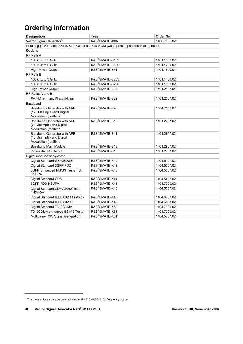
Vector Signal Generator R&S®SMATE200A Version 03.00, November 2006 58
Ordering information Designation Type Order No. Vector Signal Generator17 R&S®SMATE200A 1400.7005.02 including power cable, Quick Start Guide and CD-ROM (with operating and service manual) Options RF Path A
100 kHz to 3 GHz R&S®SMATE-B103 1401.1000.02 100 kHz to 6 GHz R&S®SMATE-B106 1401.1200.02 High-Power Output R&S®SMATE-B31 1401.1800.04
RF Path B 100 kHz to 3 GHz R&S®SMATE-B203 1401.1400.02 100 kHz to 6 GHz R&S®SMATE-B206 1401.1600.02 High-Power Output R&S®SMATE-B36 1401.2107.04
RF Paths A and B FM/ϕM and Low Phase Noise R&S®SMATE-B22 1401.2507.02
Baseband Baseband Generator with ARB (128 Msample) and Digital Modulation (realtime)
R&S®SMATE-B9 1404.7500.02
Baseband Generator with ARB (64 Msample) and Digital Modulation (realtime)
R&S®SMATE-B10 1401.2707.02
Baseband Generator with ARB (16 Msample) and Digital Modulation (realtime)
R&S®SMATE-B11 1401.2807.02
Baseband Main Module R&S®SMATE-B13 1401.2907.02 Differential I/Q Output R&S®SMATE-B16 1401.2407.02
Digital modulation systems Digital Standard GSM/EDGE R&S®SMATE-K40 1404.5107.02 Digital Standard 3GPP FDD R&S®SMATE-K42 1404.5207.02 3GPP Enhanced MS/BS Tests incl. HSDPA
R&S®SMATE-K43 1404.5307.02
Digital Standard GPS R&S®SMATE-K44 1404.5407.02 3GPP FDD HSUPA R&S®SMATE-K45 1404.7300.02 Digital Standard CDMA2000® incl. 1xEV-DV
R&S®SMATE-K46 1404.5507.02
Digital Standard IEEE 802.11 (a/b/g) R&S®SMATE-K48 1404.6703.02 Digital Standard IEEE 802.16 R&S®SMATE-K49 1404.6803.02 Digital Standard TD-SCDMA R&S®SMATE-K50 1404.7100.02 TD-SCDMA enhanced BS/MS Tests R&S®SMATE-K51 1404.7200.02 Multicarrier CW Signal Generation R&S®SMATE-K61 1404.5707.02
17 The base unit can only be ordered with an R&S®SMATE-B10x frequency option.
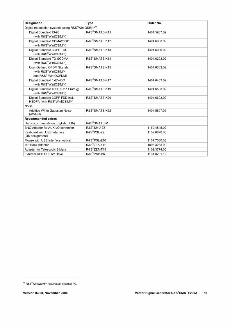
Version 03.00, November 2006 Vector Signal Generator R&S®SMATE200A 59
Designation Type Order No. Digital modulation systems using R&S®WinIQSIM™18
Digital Standard IS-95 (with R&S®WinIQSIM™)
R&S®SMATE-K11 1404.5907.02
Digital Standard CDMA2000® (with R&S®WinIQSIM™)
R&S®SMATE-K12 1404.6003.02
Digital Standard 3GPP TDD (with R&S®WinIQSIM™)
R&S®SMATE-K13 1404.6090.02
Digital Standard TD-SCDMA (with R&S®WinIQSIM™)
R&S®SMATE-K14 1404.6203.02
User-Defined OFDM Signals (with R&S®WinIQSIM™ and R&S® WinIQOFDM)
R&S®SMATE-K15 1404.6303.02
Digital Standard 1xEV-DO (with R&S®WinIQSIM™)
R&S®SMATE-K17 1404.6403.02
Digital Standard IEEE 802.11 (a/b/g) (with R&S®WinIQSIM™)
R&S®SMATE-K19 1404.6503.02
Digital Standard 3GPP FDD incl. HSDPA (with R&S®WinIQSIM™)
R&S®SMATE-K20 1404.6603.02
Noise Additive White Gaussian Noise (AWGN)
R&S®SMATE-K62 1404.5807.02
Recommended extras Hardcopy manuals (in English, USA) R&S®SMATE-M BNC Adapter for AUX I/O connector R&S®SMU-Z5 1160.4545.02 Keyboard with USB Interface (US assignment)
R&S®PSL-Z2 1157.6870.03
Mouse with USB Interface, optical R&S®PSL-Z10 1157.7060.03 19" Rack Adapter R&S®ZZA-411 1096.3283.00 Adapter for Telescopic Sliders R&S®ZZA-T45 1109.3774.00 External USB CD-RW Drive R&S®PSP-B6 1134.8201.12
18 R&S®WinIQSIM™ requires an external PC.
Certified Quality System
ISO 9001DQS REG. NO 1954 QM
Certified Environmental System
ISO 14001DQS REG. NO 1954 UM
¸ is
a re
gist
ered
trad
emar
k of
Roh
de &
Sch
war
z Gm
bH &
Co.
KG
· Tra
de n
ames
are
trad
emar
ks o
f the
ow
ners
· Pr
inte
d in
Ger
man
y (c
h)PD
075
8.18
93.2
2 · V
ersi
on 0
3.00
· N
ovem
ber 2
006
· ¸SM
ATE2
00A
· Dat
a w
ithou
t tol
eran
ce li
mits
is n
ot b
indi
ng ·
Subj
ect t
o ch
ange
For product brochure, see PD 0758.1893.12 and www.rohde-schwarz.com
(search term: SMATE200A)
www.rohde-schwarz.comEurope: +49 1805 12 4242, [email protected]
USA and Canada: +1-888-837-8772, [email protected]: +65 65 130 488, [email protected]


![Vector Signal Generator MG3710A Product Introduction · Vector Signal Generator MG3710A Features AWGN generator [Opt-049/079] AM/FM/ M/PM Functions [Standard] Additional analog modulation](https://img.pdfslide.net/doc/110x75/5eb581a18015c7750f3b383c/vector-signal-generator-mg3710a-product-introduction-vector-signal-generator-mg3710a.jpg)