Embed Size (px)
Citation preview

GPS Venus838FLPx Breakout Board
(v1.2)
Released under the Creative Commons Attribution Share-Alike 3.0 License
http://creativecommons.org/licenses/by-sa/3.0/

Overview
SkyTraq has introduced the fastest consumer grade GPS receiver available. The Venus838FLPx
GPS receiver module has industry leading 50Hz update rate, very fast and accurate
position/speed response, suitable for UAV, RC plane flight logging, and high-performance race
car or speed boat data logging applications. When running at lower 1Hz, 5Hz, or 10Hz update
rate, the Venus838FLPx receiver can be used as a typical GPS receiver module currently
available on the market.
The break-out board includes mounting pads for a small lithium battery allowing for quick re-
acquisition (1 second) on power up. Typical data retention times are several days depending
on the lithium battery. Lithium battery not included.
Features
• 50 Hz Maximum Update Rate
• I2C, SPI Interface
• Supports optional lithium battery backup
• Support QZSS, SBAS
• 16 million time-frequency hypothesis testing per sec
• -148dBm cold start sensitivity
• -165dBm tracking sensitivity
• 29 second cold start TTFF
• 3.5 second TTFF with AGPS
• 1 second hot start
• 2.5m CEP accuracy
• Multipath detection and suppression
• Jamming detection and mitigation
• 7-day extended ephemeris AGPS
Tech Specs
• Dynamics: 4G (39.2m/sec2)
• Operational Limits: Altitude < 18,000m or velocity < 515m/s, not exceeding both
• Update Rates: 1 / 2 / 4 / 5 / 8 / 10 / 20 / 25 / 40 / 50 Hz
• Serial Interface: 3.3V LVTTL
• Protocol: NMEA-0183 V3.01, SkyTraq binary, 9600 baud, 8, N, 1
• Input Voltage 3.3VDC +/-10%
• Acquisition Current: 32mA
• Tracking Current: 25mA
• Dimension 21mm W x 30mm L
• Weight: ~4g
• Operating Temperature -40°C ~ +85°C
Default Configuration Parameters
Baud Rate: 9600
Position Update Rate: 1Hz
Datum: WGS-84
Message Type: NMEA
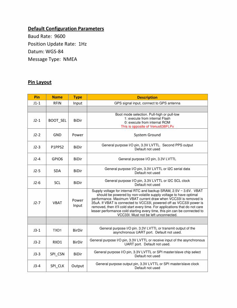
Pin Layout
Pin Name Type Description
J1-1 RFIN Input GPS signal input, connect to GPS antenna
J2-1 BOOT_SEL BiDir
Boot mode selection. Pull-high or pull-low 1: execute from internal Flash 0: execute from internal ROM
This is opposite of Venus638FLPx
J2-2 GND Power System Ground
J2-3 P1PPS2 BiDir General purpose I/O pin, 3.3V LVTTL. Second PPS output
Default not used
J2-4 GPIO6 BiDir General purpose I/O pin, 3.3V LVTTL
J2-5 SDA BiDir General purpose I/O pin, 3.3V LVTTL or I2C serial data
Default not used
J2-6 SCL BiDir General purpose I/O pin, 3.3V LVTTL or I2C SCL clock
Default not used
J2-7 VBAT Power
Input
Supply voltage for internal RTC and backup SRAM, 2.5V ~ 3.6V. VBAT should be powered by non-volatile supply voltage to have optimal
performance. Maximum VBAT current draw when VCC33I is removed is 35uA. If VBAT is connected to VCC33I, powered off as VCC33I power is removed, then it’ll cold start every time. For applications that do not care lesser performance cold starting every time, this pin can be connected to
VCC33I. Must not be left unconnected.
J3-1 TXD1 BirDir General purpose I/O pin. 3.3V LVTTL or transmit output of the
asynchronous UART port. Default not used.
J3-2 RXD1 BirDir General purpose I/O pin, 3.3V LVTTL or receive input of the asynchronous
UART port. Default not used.
J3-3 SPI_CSN BiDir General purpose I/O pin, 3.3V LVTTL or SPI master/slave chip select
Default not used
J3-4 SPI_CLK Output General purpose output pin, 3.3V LVTTL or SPI master/slave clock
Default not used

J3-5 P1PPS BiDir 1 pulse per second output. Active after position fix; goes HIGH for about
4msec, 3.3V LVTTL (default) or general purpose I/O pin
J3-6 MISO BiDir General purpose I/O pin, 3.3V LVTTL or SPI master/slave data input
Default not used
J3-7 MOSI BiDir General purpose I/O pin, 3.3V LVTTL or SPI master/slave data output
Default not used
J4-1 3.3V Power Main voltage supply input, 2.8V ~ 3.6V
J4-2 TXD0 Output Transmit output of the asynchronous UART port. Used to output standard NMEA-0183 sentence or response to input binary command. 3.3V LVTTL
J4-3 RXD0 Input Received input of the asynchronous UART port. Used to input binary
command to the GPS receiver. 3.3V LVTTL
J4-4 GND Power System Ground
J4-5 RSTN Input Active LOW reset input, 3.3V LVTTL
J4-6 GND Power System Ground

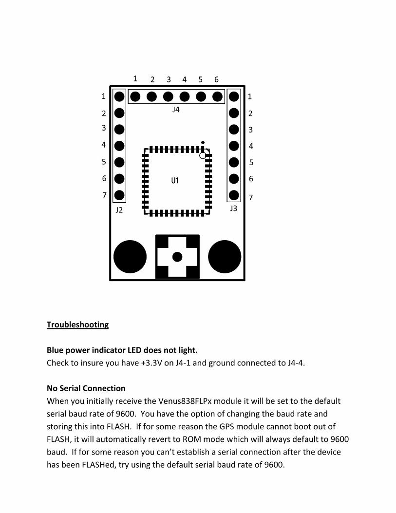
Mechanical Drawing
Troubleshooting
Blue power indicator LED does not light.
Check to insure you have +3.3V on J4-1 and ground connected to J4-4.
No Serial Connection
When you initially receive the Venus838FLPx module it will be set to the default
serial baud rate of 9600. You have the option of changing the baud rate and
storing this into FLASH. If for some reason the GPS module cannot boot out of
FLASH, it will automatically revert to ROM mode which will always default to 9600
baud. If for some reason you can’t establish a serial connection after the device
has been FLASHed, try using the default serial baud rate of 9600.

No Serial Output
The Venus838FLPx module is sensitive to slow rising power on startup. There is a
resistor and capacitor connected to J4-5 to hold the reset line low until the power
supply levels are within spec. In the event that your power supply rise time was
not within spec by the time J4-5 was considered “HIGH”, then the Venus838FLPx
module may fail to start. Try grounding J4-5 (RSTN) of the board momentarily to
reset the module.
How to load firmware
1. Launch the GNSS Viewer software and find the “Download” section
in the lower center of the application.

2. Choose your download speed. First try starting with the fastest
speed of 921600. If you have problems downloading the firmware,
then lower the speed and try again.
3. Choose your firmware file.
4. Click on the download button to start the process.
5. Once complete, your GPS receiver will reset and start operations.
How to change the NMEA data rate
1. Launch the GNSS Viewer software and click on the “Binary” drop
down menu.

2. Select “Configure Position Update Rate” and a new popup window
will appear
3. Choose the update rate required for your application (note: higher
update rates will also trigger an update to your serial transfer speeds
in order to handle the additional data)
4. Choose whether to update to SRAM only or SRAM and FLASH.
5. Select “ok” to accept the new settings.