Embed Size (px)
Citation preview
EC2155 CIRCUITS AND DEVICES LABORATORY 0 0 3
100
1 1. Verification of KVL and KCL
2 2. Verification of Thevenin and Norton Theorems.
3 3. Verification of superposition Theorem.
4 4. Verification of Maximum power transfer and reciprocity theorems.
5 5. Frequency response of series and parallel resonance circuits.
6 6. Characteristics of PN and Zener diode
7 7. Characteristics of CE configuration
8 8. Characteristics of CB configuration
9 9. Characteristics of UJT and SCR
10 10. Characteristics of JFET and MOSFET
11 11. Characteristics of Diac and Triac.
12 12. Characteristics of Photodiode and Phototransistor.
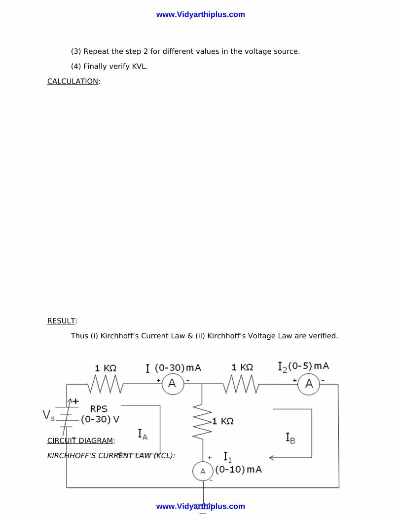
VERIFICATION OF KCL & KVL (KIRCHHOFF’S LAWS)
www.Vidyarthiplus.com
www.Vidyarthiplus.com

AIM:
To verify (i) Kirchhoff’s current law (KCL) (ii) Kirchhoff’s voltage law (KCL)
EQUIPMENTS & COMPONENTS REQUIRED:
Sl. No.
Equipments & Components
Range Quantity
1 RPS (0-30) V 12 Ammeter (0-5) mA, (0-10) mA, (0-30)
mA2, 2, 1 respectively
3 Voltmeter (0-10) V 34 Resistor 1 KΩ 55 Bread Board 16 Connecting wires As required
THEORY:
KIRCHHOFF’S CURRENT LAW (KCL):
KCL states that “the algebraic sum of all the currents at any node in a circuit equals zero”.
i.e., Sum of all currents entering a node = Sum of all currents leaving a node
KIRCHHOFF’S VOLTAGE LAW (KVL):
KVL states that “the algebraic sum of all the voltages around any closed loop in a circuit equals zero”.
i.e., Sum of voltage drops = Sum of voltage rises
PROCERURE:
KIRCHHOFF’S CURRENT LAW (KCL):
(1) Connect the components as shown in the circuit diagram.
(2) Switch on the DC power supply and note down the corresponding ammeter readings.
(3) Repeat the step 2 for different values in the voltage source.
(4) Finally verify KCL.
KIRCHHOFF’S VOLTAGE LAW (KVL):
(1) Connect the components as shown in the circuit diagram.
(2) Switch on the DC power supply and note down the corresponding voltmeter readings.
www.Vidyarthiplus.com
www.Vidyarthiplus.com
(3) Repeat the step 2 for different values in the voltage source.
(4) Finally verify KVL.
CALCULATION:
RESULT:
Thus (i) Kirchhoff’s Current Law & (ii) Kirchhoff’s Voltage Law are verified.
CIRCUIT DIAGRAM:
KIRCHHOFF’S CURRENT LAW (KCL):
www.Vidyarthiplus.com
www.Vidyarthiplus.com
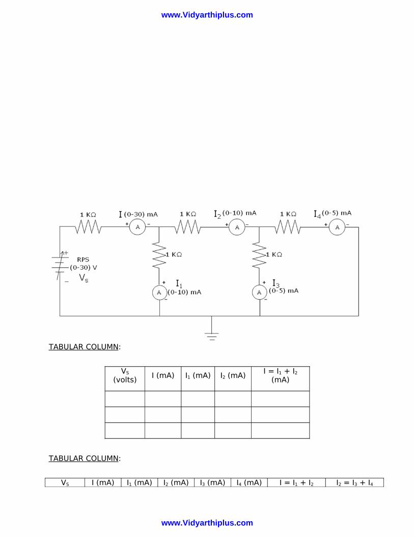
TABULAR COLUMN:
VS
(volts)I (mA) I1 (mA) I2 (mA)
I = I1 + I2
(mA)
TABULAR COLUMN:
VS I (mA) I1 (mA) I2 (mA) I3 (mA) I4 (mA) I = I1 + I2 I2 = I3 + I4
www.Vidyarthiplus.com
www.Vidyarthiplus.com
(volts) (mA) (mA)
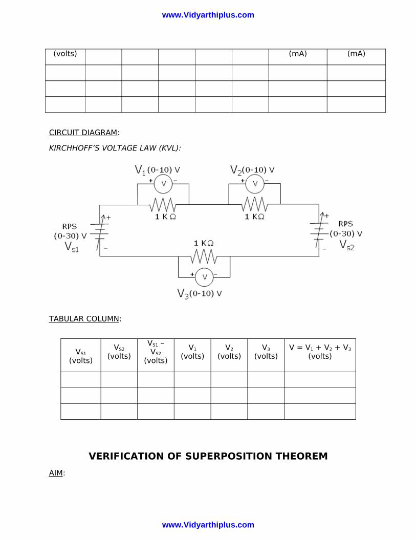
CIRCUIT DIAGRAM:
KIRCHHOFF’S VOLTAGE LAW (KVL):
TABULAR COLUMN:
VS1
(volts)
VS2
(volts)
VS1 – VS2
(volts)
V1
(volts)V2
(volts)V3
(volts)V = V1 + V2 + V3
(volts)
VERIFICATION OF SUPERPOSITION THEOREM
AIM:
www.Vidyarthiplus.com
www.Vidyarthiplus.com
To verify Superposition theorem for (i) Symmetrical T- Network (ii) Asymmetrical T- Network (iii) Symmetrical π Network
EQUIPMENTS & COMPONENTS REQUIRED:
Sl. No.
Equipments & Components
Range Quantity
1 RPS (0-30) V 12 Ammeter (0-1) mA, (0-10) mA 1 each3 Resistor 10 KΩ, 22 KΩ, 5.8 KΩ, 1
Ω3, 1, 1, 1 respectively
4 Bread Board 15 Connecting wires As required
THEORY:
SUPERPOSITION THEOREM:
Superposition theorem states that “in any linear network containing two or more sources, the response in any element is equal to the algebraic sum of the responses caused by the individual sources acting alone, while the other sources are non-operative”.
While considering the effect of individual sources, other ideal voltage and current sources in the network are replaced by short circuit and open circuit across the terminal respectively.
PROCEDURE:
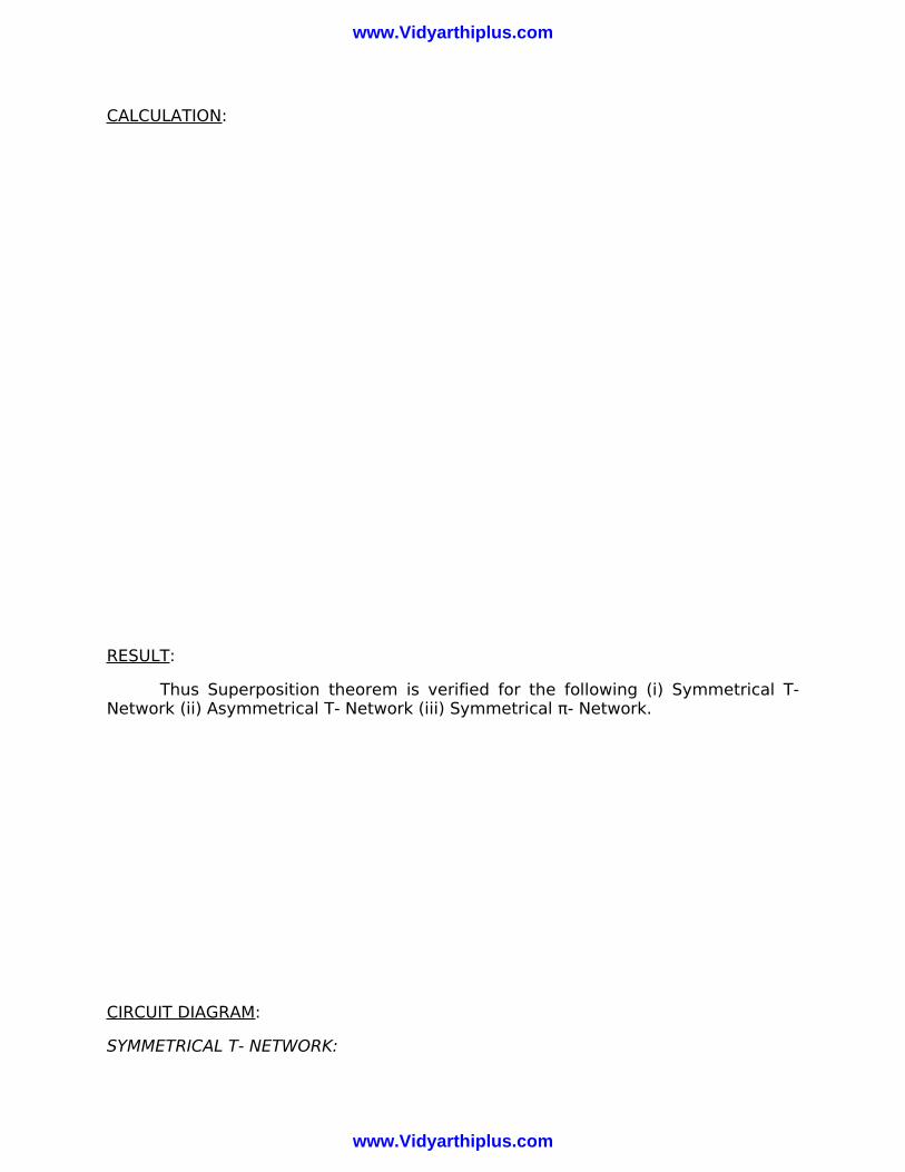
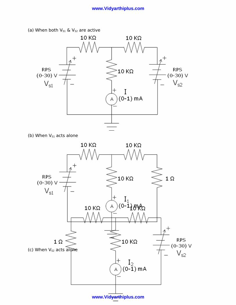
(1) Connect the components as shown in the circuit diagram.
(2) Switch on the DC power supplies VS1 & VS2 (e.g.: to 10 V & 5 V) and note down the corresponding ammeter reading. Let this current be I.
(3) Replace the power supply VS2 (5 V) by its internal resistance and then switch on the supply VS1 (10 V) and note down the corresponding ammeter reading. Let this current be I1.
(4) Now connect back the power supply VS2 (5 V) and replace the supply VS1
(10 V) by its internal resistance.
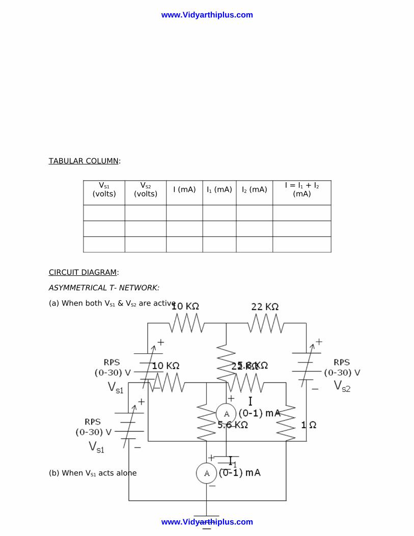
(5) Switch on the supply VS2 (5 V) and note down the corresponding ammeter reading. Let this current be I2.
(6) Repeat the steps 2 to 5 for different values of VS1 & VS2.
(7) Verify the theorem using the relation I = I1 + I2 (for T- Network) & I = I1 ~ I2 (for Symmetrical π- Network)
www.Vidyarthiplus.com
www.Vidyarthiplus.com
CALCULATION:
RESULT:
Thus Superposition theorem is verified for the following (i) Symmetrical T- Network (ii) Asymmetrical T- Network (iii) Symmetrical π- Network.
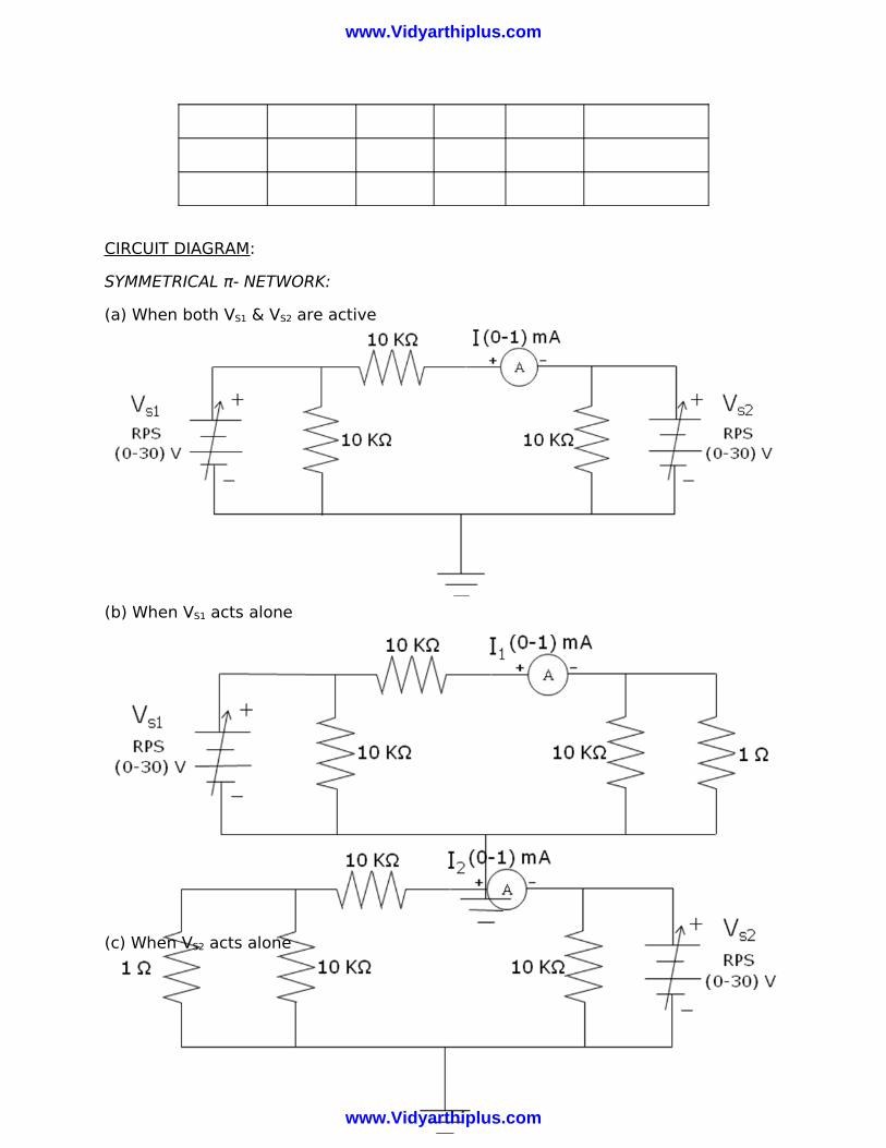
CIRCUIT DIAGRAM:
SYMMETRICAL T- NETWORK:
www.Vidyarthiplus.com
www.Vidyarthiplus.com
(a) When both VS1 & VS2 are active
(b) When VS1 acts alone
(c) When VS2 acts alone
www.Vidyarthiplus.com
www.Vidyarthiplus.com
TABULAR COLUMN:
VS1
(volts)VS2
(volts)I (mA) I1 (mA) I2 (mA)
I = I1 + I2
(mA)
CIRCUIT DIAGRAM:
ASYMMETRICAL T- NETWORK:
(a) When both VS1 & VS2 are active
(b) When VS1 acts alone
www.Vidyarthiplus.com
www.Vidyarthiplus.com
(c) When VS2 acts alone
TABULAR COLUMN:
VS1
(volts)VS2
(volts)I (mA) I1 (mA) I2 (mA)
I = I1 + I2
(mA)
www.Vidyarthiplus.com
www.Vidyarthiplus.com
CIRCUIT DIAGRAM:
SYMMETRICAL π- NETWORK:
(a) When both VS1 & VS2 are active
(b) When VS1 acts alone
(c) When VS2 acts alone
www.Vidyarthiplus.com
www.Vidyarthiplus.com

TABULAR COLUMN:
VS1
(volts)VS2
(volts)I (mA) I1 (mA) I2 (mA)
I = I1 ~ I2
(mA)
VERIFICATION OF THEVENIN’S & NORTON’S THEOREM
AIM:
To verify Thevenin’s & Norton’s theorem using experimental set up.
EQUIPMENTS & COMPONENTS REQUIRED:
www.Vidyarthiplus.com
www.Vidyarthiplus.com
Sl. No.
Equipments & Components
Range Quantity
1 RPS (0-30) V 12 Voltmeter (0-10) V 13 Ammeter (0-1) mA 14 Resistor 1 KΩ, 560 Ω, 470 Ω, 1 Ω,
829.10 Ω, 10 KΩ, 5.6 KΩ, 5.1 KΩ
2, 1, 1, 1, 1, 3, 2, 1 respectively
5 Bread Board 16 Connecting wires As required
THEORY:
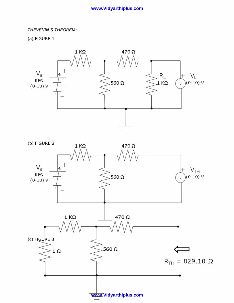
THEVENIN’S THEOREM:
Thevenin’s theorem states that “any two terminal linear network having a number of voltage, current sources and resistances can be replaced by a simple equivalent circuit consisting of a single voltage source in series with a resistance”, where the value of the voltage source is equal to the open circuit voltage across the two terminals of the network, and resistance is equal to the equivalent resistance measured between the terminals with all the energy sources replaced by their internal resistances.
NORTON’S THEOREM:
Norton’s theorem states that “any two terminal linear network having a number of voltage, current sources and resistances can be replaced by an equivalent circuit consisting of a single current source in parallel with a resistance”. The value of the current source is the short circuit current between the two terminals of the network, and resistance is the equivalent resistance measured between the terminals of the network with all the energy sources replaced by their internal resistances.
PROCEDURE:
THEVENIN’S THEOREM:
General Circuit:
(1) Connect the components as shown in the circuit diagram 1.
(2) Measure the voltage across the load using a voltmeter or multimeter after switching on the power supply. Let it be VL.
To find Thevenin’s Voltage: (VTH)
(1) Connect the components as shown in the circuit diagram 2.
(2) Remove the load resistance and measure the open circuited voltage VTH
across the output terminal.
www.Vidyarthiplus.com
www.Vidyarthiplus.com
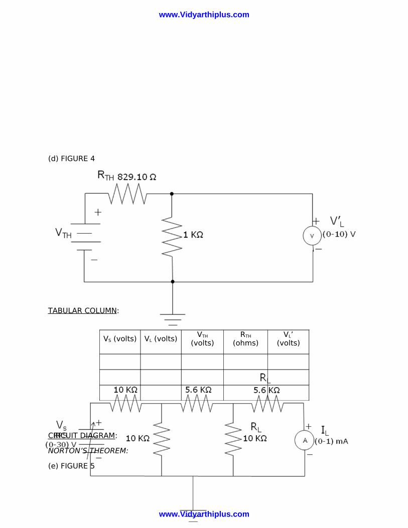
To find Thevenin’s Resistance: (RTH)
(1) Connect the components as shown in the circuit diagram 3.
(2) Remove the voltage source and replace it with an internal resistance as shown.
(3) Using multimeter in resistance mode, measure the resistance across the output terminal.
Thevenin’s Circuit:
(1) Connect the power supply of VTH and resistance of RTH in series as shown in the circuit diagram 4.
(2) Connect the load resistance RL and measure VL’ across the load resistance using a voltmeter after switching on the power supply.
(3) Voltage measured with figure 1 should be equal to the voltage measured with this circuit. (i.e., VL = VL’)
NORTON’S THEOREM:
General Circuit:
(1) Connect the components as shown in the circuit diagram 5.
(2) Measure the current through the load using an ammeter or multimeter after switching on the power supply. Let it be IL.
To find Norton’s Current: (IN)
(1) Connect the components as shown in the circuit diagram 6.
(2) Remove the load resistance and short circuit the output terminal. Then measure the current through the short circuited terminals.
To find Norton’s Resistance: (RN)
(1) Connect the components as shown in the circuit diagram 7.
(2) Remove the voltage source and replace it with an internal resistance as shown.
(3) Using multimeter in resistance mode, measure the resistance across the output terminal.
Norton’s Circuit:
(1) Draw the short circuit current source IN in parallel with RN as shown in the circuit diagram 8.
www.Vidyarthiplus.com
www.Vidyarthiplus.com

(2) Draw the equivalent circuit by replacing the current source IN in parallel with RN by a voltage source such that Veq = IN . RN volts.
(3) Then connect the circuit as shown in figure 9 and measure the load current IL’ through the load resistor RL. This must be equal to IL.
CALCULATION:
RESULT:
Thus Thevenin’s theorem & Norton’s theorem are verified.
CIRCUIT DIAGRAM:
www.Vidyarthiplus.com
www.Vidyarthiplus.com
THEVENIN’S THEOREM:
(a) FIGURE 1
(b) FIGURE 2
(c) FIGURE 3
www.Vidyarthiplus.com
www.Vidyarthiplus.com
(d) FIGURE 4
TABULAR COLUMN:
VS (volts) VL (volts)VTH
(volts)RTH
(ohms)VL’
(volts)
CIRCUIT DIAGRAM:
NORTON’S THEOREM:
(e) FIGURE 5
www.Vidyarthiplus.com
www.Vidyarthiplus.com
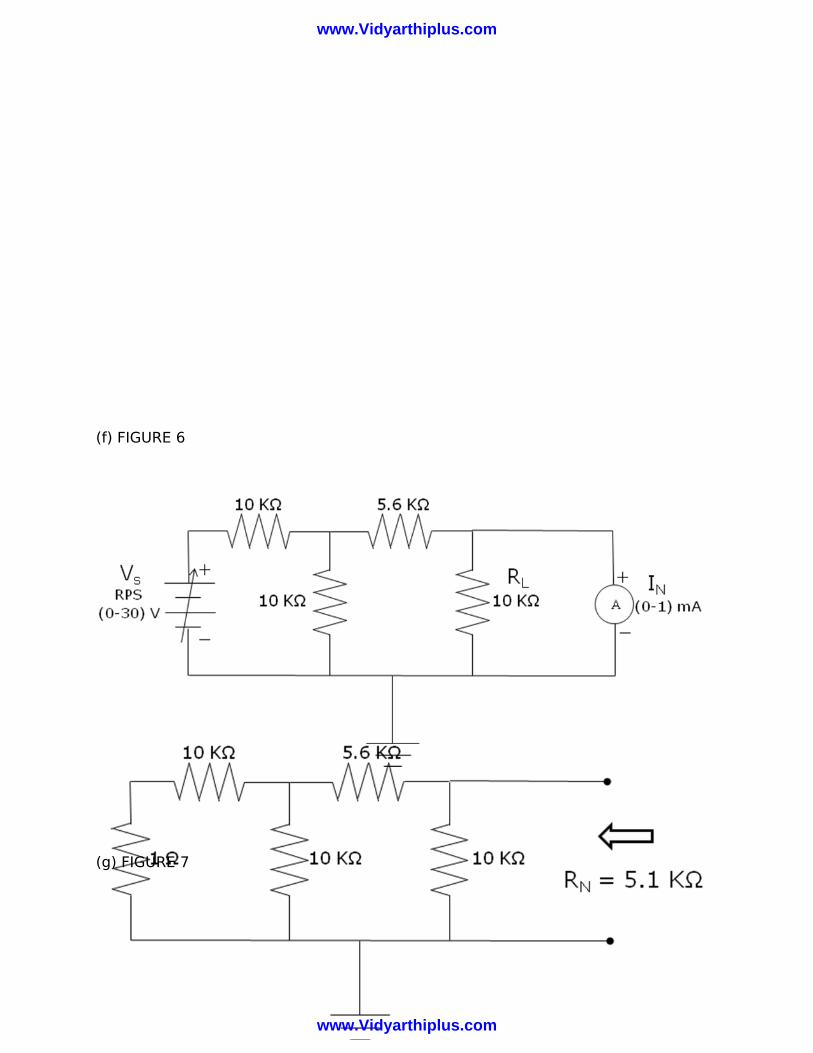
(f) FIGURE 6
(g) FIGURE 7
www.Vidyarthiplus.com
www.Vidyarthiplus.com
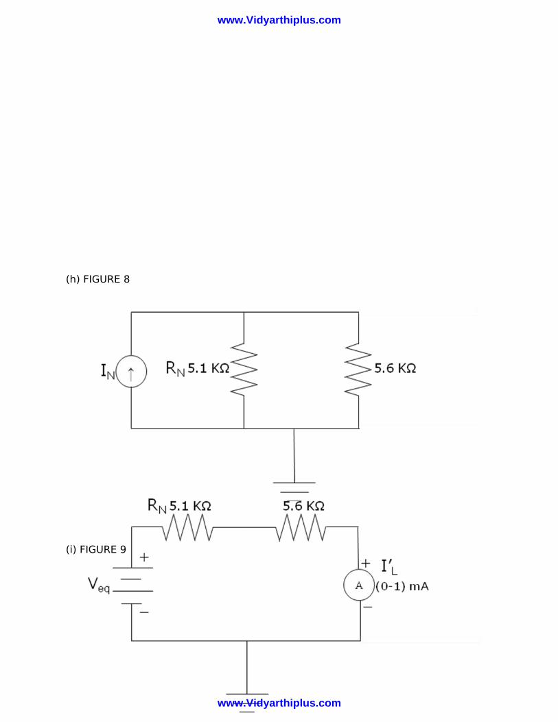
(h) FIGURE 8
(i) FIGURE 9
www.Vidyarthiplus.com
www.Vidyarthiplus.com
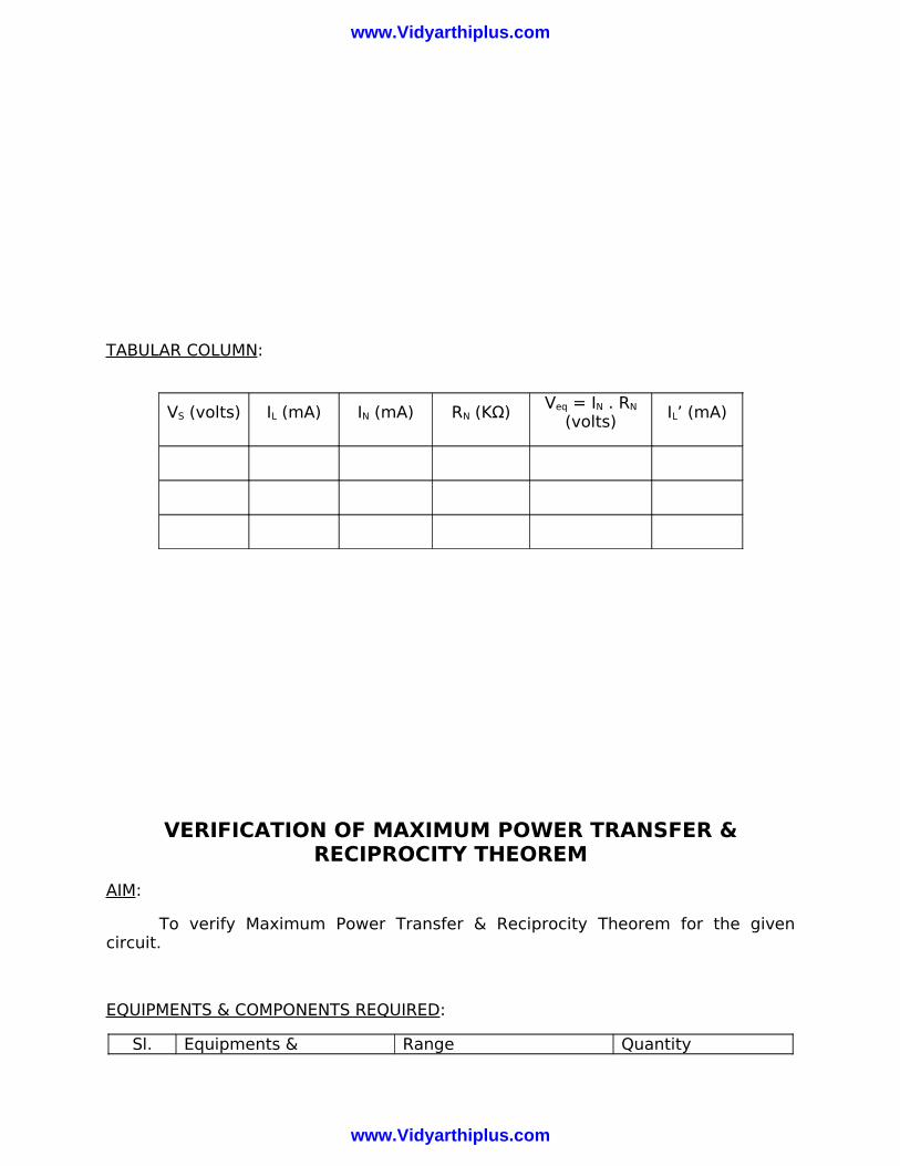
TABULAR COLUMN:
VS (volts) IL (mA) IN (mA) RN (KΩ)Veq = IN . RN
(volts)IL’ (mA)
VERIFICATION OF MAXIMUM POWER TRANSFER & RECIPROCITY THEOREM
AIM:
To verify Maximum Power Transfer & Reciprocity Theorem for the given circuit.
EQUIPMENTS & COMPONENTS REQUIRED:
Sl. Equipments & Range Quantity
www.Vidyarthiplus.com
www.Vidyarthiplus.com
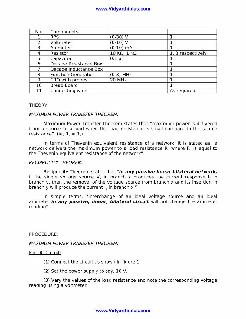
No. Components1 RPS (0-30) V 12 Voltmeter (0-10) V 13 Ammeter (0-10) mA 14 Resistor 10 KΩ, 1 KΩ 1, 3 respectively5 Capacitor 0.1 μF 16 Decade Resistance Box 17 Decade Inductance Box 18 Function Generator (0-3) MHz 19 CRO with probes 20 MHz 1
10 Bread Board 111 Connecting wires As required
THEORY:
MAXIMUM POWER TRANSFER THEOREM:
Maximum Power Transfer Theorem states that “maximum power is delivered from a source to a load when the load resistance is small compare to the source resistance”. (ie, RL = RS)
In terms of Thevenin equivalent resistance of a network, it is stated as “a network delivers the maximum power to a load resistance RL where RL is equal to the Thevenin equivalent resistance of the network”.
RECIPROCITY THEOREM:
Reciprocity Theorem states that “in any passive linear bilateral network, if the single voltage source Vx in branch x produces the current response Iy in branch y, then the removal of the voltage source from branch x and its insertion in branch y will produce the current Iy in branch x.”
In simple terms, “interchange of an ideal voltage source and an ideal ammeter in any passive, linear, bilateral circuit will not change the ammeter reading”.
PROCEDURE:
MAXIMUM POWER TRANSFER THEOREM:
For DC Circuit:
(1) Connect the circuit as shown in figure 1.
(2) Set the power supply to say, 10 V.
(3) Vary the values of the load resistance and note the corresponding voltage reading using a voltmeter.
www.Vidyarthiplus.com
www.Vidyarthiplus.com
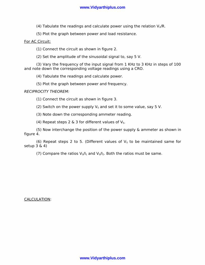
(4) Tabulate the readings and calculate power using the relation V2/R.
(5) Plot the graph between power and load resistance.
For AC Circuit:
(1) Connect the circuit as shown in figure 2.
(2) Set the amplitude of the sinusoidal signal to, say 5 V.
(3) Vary the frequency of the input signal from 1 KHz to 3 KHz in steps of 100 and note down the corresponding voltage readings using a CRO.
(4) Tabulate the readings and calculate power.
(5) Plot the graph between power and frequency.
RECIPROCITY THEOREM:
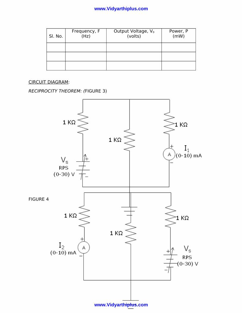
(1) Connect the circuit as shown in figure 3.
(2) Switch on the power supply VS and set it to some value, say 5 V.
(3) Note down the corresponding ammeter reading.
(4) Repeat steps 2 & 3 for different values of VS.
(5) Now interchange the position of the power supply & ammeter as shown in figure 4.
(6) Repeat steps 2 to 5. (Different values of VS to be maintained same for setup 3 & 4)
(7) Compare the ratios VS/I1 and VS/I2. Both the ratios must be same.
CALCULATION:
www.Vidyarthiplus.com
www.Vidyarthiplus.com
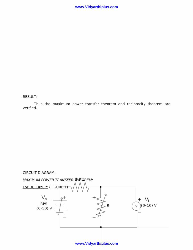
RESULT:
Thus the maximum power transfer theorem and reciprocity theorem are verified.
CIRCUIT DIAGRAM:
MAXIMUM POWER TRANSFER THEOREM:
For DC Circuit: (FIGURE 1)
www.Vidyarthiplus.com
www.Vidyarthiplus.com
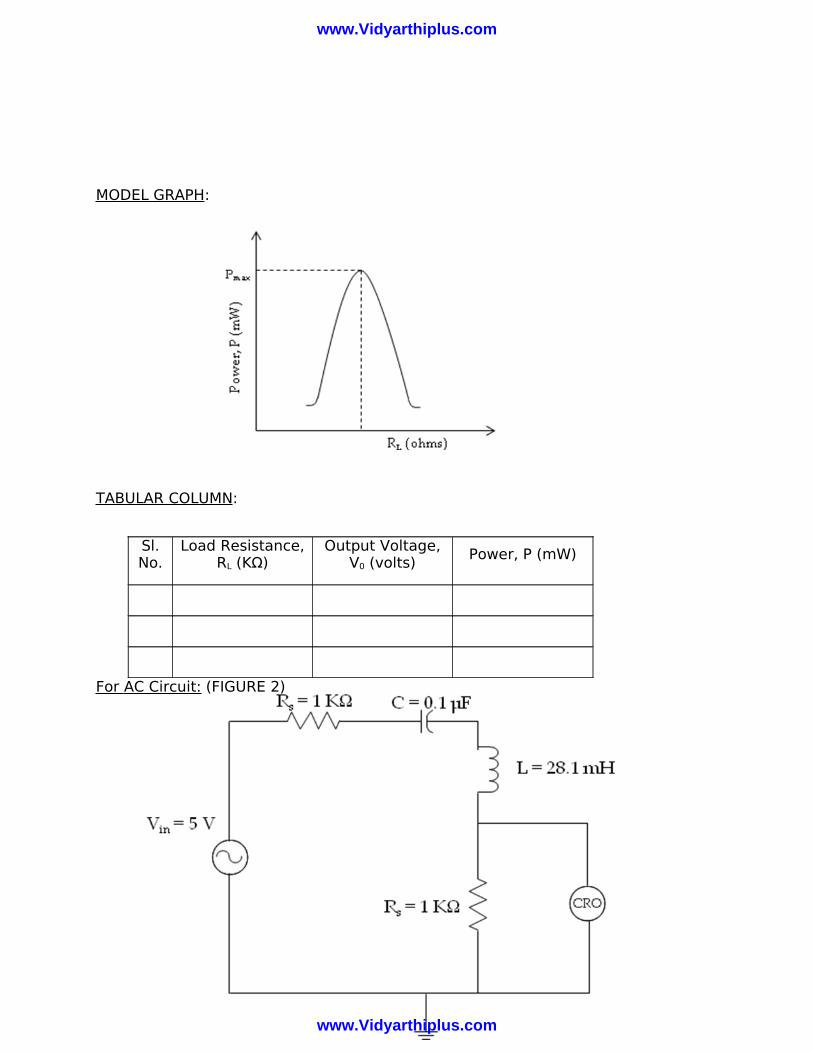
MODEL GRAPH:
TABULAR COLUMN:
Sl. No.
Load Resistance, RL (KΩ)
Output Voltage, V0 (volts)
Power, P (mW)
For AC Circuit: (FIGURE 2)
www.Vidyarthiplus.com
www.Vidyarthiplus.com
Design:
The maximum power is transferred if the following is satisfied. i.e., XC = XL.
where 0
1
2CX F Cπ=
02LX F Lπ=
From these we have,
0
1
2F
LCπ=
Considering F0 = 3 KHz & C = 0.1 μF i.e., 0.1 x 10⁻⁶ F
2 20
1
4L
F Cπ=
( ) ( )2 6 6
1
4 9 *10 0.1*10L
π −= = 28.1 mH
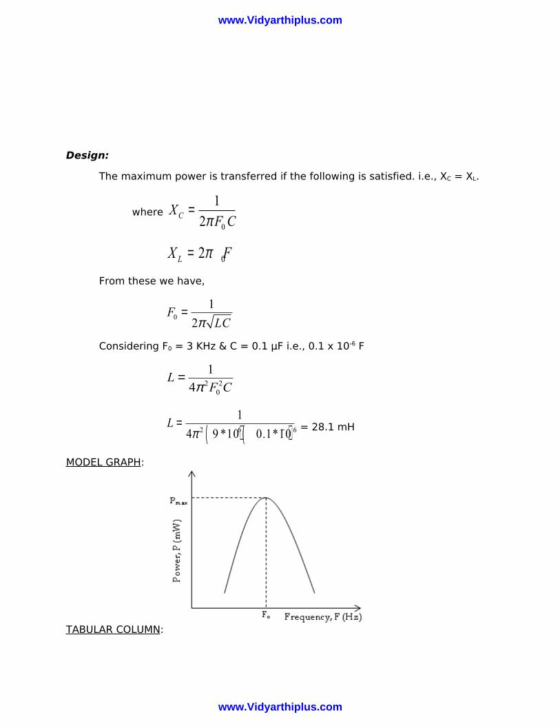
MODEL GRAPH:
TABULAR COLUMN:
www.Vidyarthiplus.com
www.Vidyarthiplus.com
Sl. No.Frequency, F
(Hz)Output Voltage, V0
(volts)Power, P
(mW)
CIRCUIT DIAGRAM:
RECIPROCITY THEOREM: (FIGURE 3)
FIGURE 4
www.Vidyarthiplus.com
www.Vidyarthiplus.com
TABULAR COLUMN:
VS (volts) I1 (mA) VS/I1 (Ω) I2 (mA) VS/I1 (Ω)
FREQUENCY RESPONSE OF SERIES AND PARALLEL RESONANCE CIRCUITS
AIM:
To plot the resonance curve and to determine the bandwidth & Q-factor of series and parallel resonance circuit.
EQUIPMENTS & COMPONENTS REQUIRED:
Sl. No.
Equipments & Components
Range Quantity
1 Function Generator (0-3) MHz 12 CRO with probes 20 MHz 13 Resistor 1 KΩ 14 Capacitor 0.1 μF 15 Decade Inductance Box 1
www.Vidyarthiplus.com
www.Vidyarthiplus.com
6 Bread Board 17 Connecting wires As required
DESIGN:
PARALLEL RESONANT CIRCUIT:
For a parallel resonant circuit, at resonance, XC = XL.
Resonant frequency is 1
2rf
LCπ=
Considering fr = 3 KHz & C = 0.1 μF i.e., 0.1 x 10⁻⁶ F
2 2
1
4 r
Lf Cπ
=
( ) ( )2 6 6
1
4 9 *10 0.1*10L
π −= = 28.1 mH
Quality factor is obtained by, rfQ factorBW
− = where BW is bandwidth, which
is the difference between the upper cutoff, (f2) and lower cutoff frequencies (f1) i.e., f2 - f1
SERIES RESONANT CIRCUIT:
For a series resonant circuit, resonant frequency is obtained as follows,
At resonance, XC = XL
where 1
2Cr
Xf Cπ
=
2L rX f Lπ=
Therefore, 1
2rf
LCπ=
Considering fr = 3 KHz & C = 0.1 μF i.e., 0.1 x 10⁻⁶ F
www.Vidyarthiplus.com
www.Vidyarthiplus.com
2 2
1
4 r
Lf Cπ
=
( ) ( )2 6 6
1
4 9 *10 0.1*10L
π −= = 28.1 mH
Quality factor is obtained by, rfQ factorBW
− = where BW is bandwidth, which
is the difference between the upper cutoff, (f2) and lower cutoff frequencies (f1) i.e., f2 - f1
PROCEDURE:
(1) Connect the circuit as shown in figure.
(2) Set to amplitude of the sinusoidal signal to 5 V, say.
(3) Frequency of the input signal is varied from 100 Hz to 2 KHz. Note down the corresponding voltages on CRO for different frequencies.
(4) Tabulate the readings and calculate the current using the formula I = V0/R (mA).
(5) Plot the graph between voltage measured and frequency.
(6) Draw a horizontal line exactly at √2 times the peak value, which intersects the curve at two points. Draw a line from intersecting points to x-axis which meets at f1 and f2.
(7) The bandwidth and Q-factor is obtained from the formula given above.
CALCULATION:
www.Vidyarthiplus.com
www.Vidyarthiplus.com
RESULT:
Thus the resonance curve is plotted and bandwidth & Q-factor is determined for the parallel and series resonance circuits.
Parallel Resonance Circuit
Series Resonance Circuit
Bandwidth (BW in Hz)
Q-factor
CIRCUIT DIAGRAM:
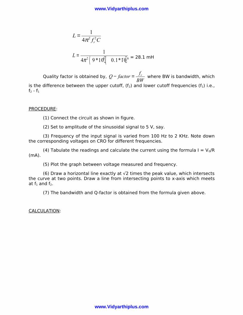
PARALLEL RESONANCE CIRCUIT: (FIGURE 1)
www.Vidyarthiplus.com
www.Vidyarthiplus.com
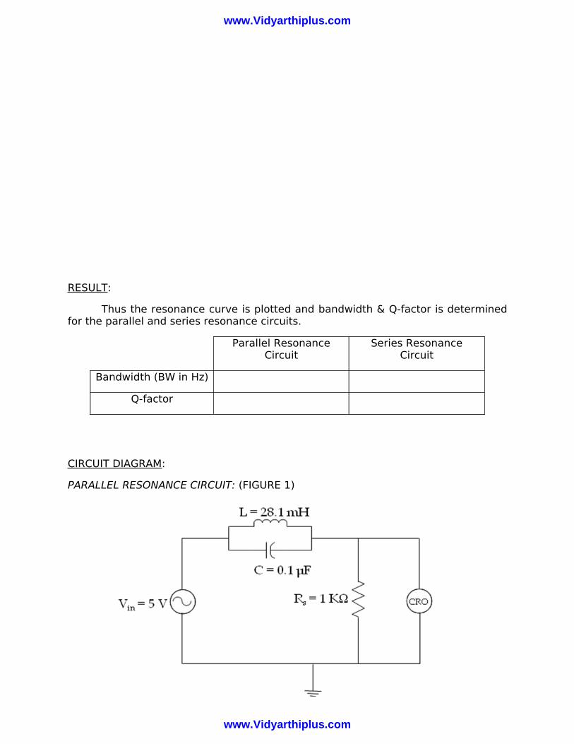
MODEL GRAPH:
TABULAR COLUMN:
Sl. No.
Frequency, F (Hz)
Output Voltage, V0
(volts)Current, I (mA)
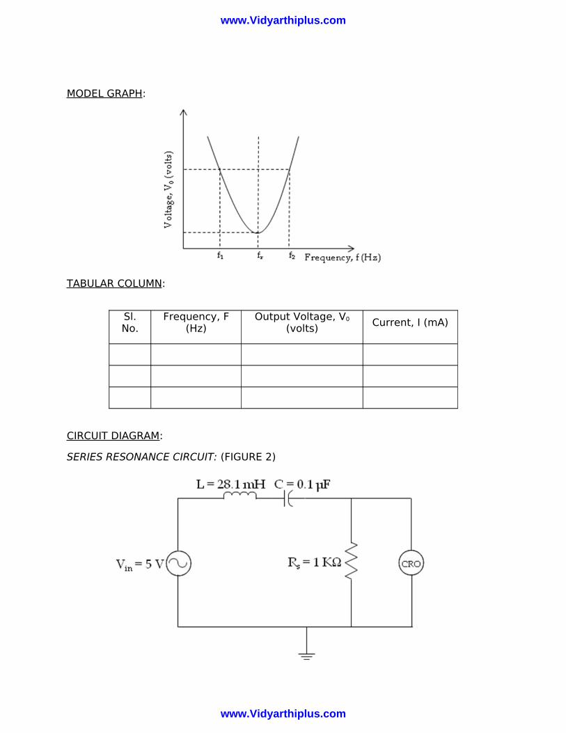
CIRCUIT DIAGRAM:
SERIES RESONANCE CIRCUIT: (FIGURE 2)
www.Vidyarthiplus.com
www.Vidyarthiplus.com
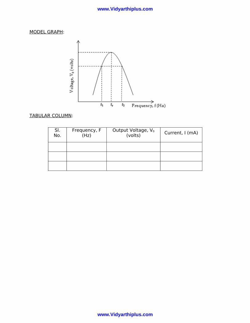
MODEL GRAPH:
TABULAR COLUMN:
Sl. No.
Frequency, F (Hz)
Output Voltage, V0
(volts)Current, I (mA)
www.Vidyarthiplus.com
www.Vidyarthiplus.com