Embed Size (px)
Citation preview
VerilogVerilog CodingCodingREF: • Reuse Methodology Manual – For System-ON-A-Chip Design, Third Edition 2002• CIC Training Manual – Logic Synthesis with Design Compiler, July, 2007• Hsing-Chen, Lu, “ARES Lab 2008 Summer Training Course of Verilog Coding Style”s g C e , u, S ab 008 Su e a g Cou se o e og Cod g Sty e• Hsi-Pin, Ma, “LARC Lab Training Course of Design Concept and Coding Style”
2010.12.01Advanced Reliable Systems (ARES) Lab.
1
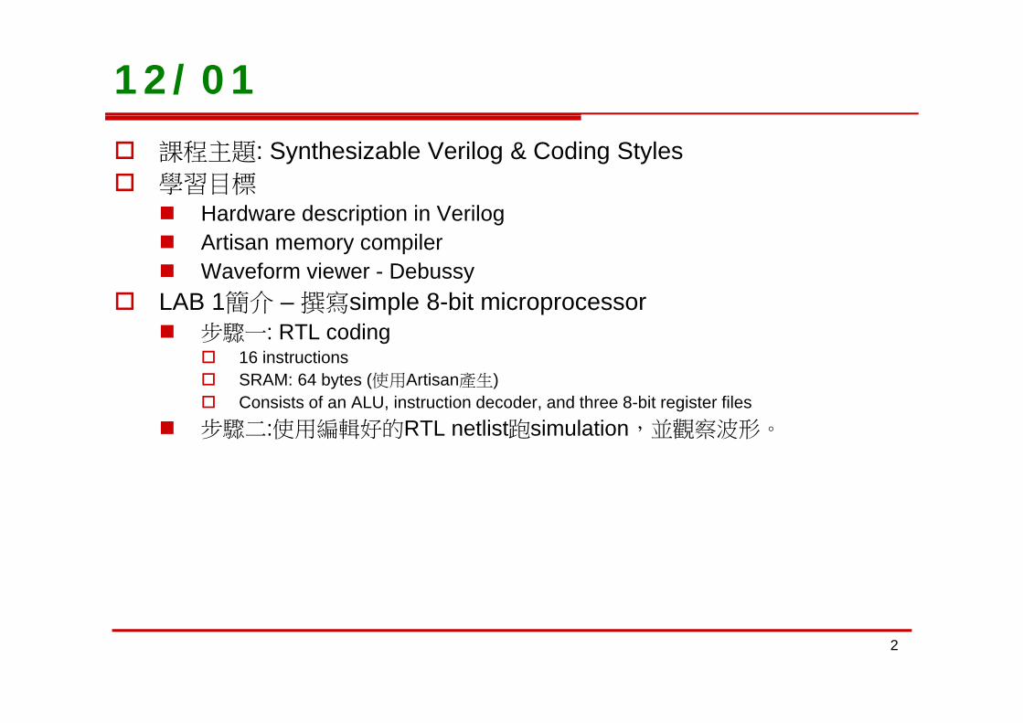
12/01 課程主題: Synthesizable Verilog & Coding Styles 學習目標
Hardware description in Verilog Artisan memory compiler Waveform viewer - Debussyy
LAB 1簡介 – 撰寫simple 8-bit microprocessor 步驟一: RTL coding
16 instructions 16 instructions SRAM: 64 bytes (使用Artisan產生) Consists of an ALU, instruction decoder, and three 8-bit register files
步驟二:使用編輯好的RTL netlist跑simulation,並觀察波形。
2
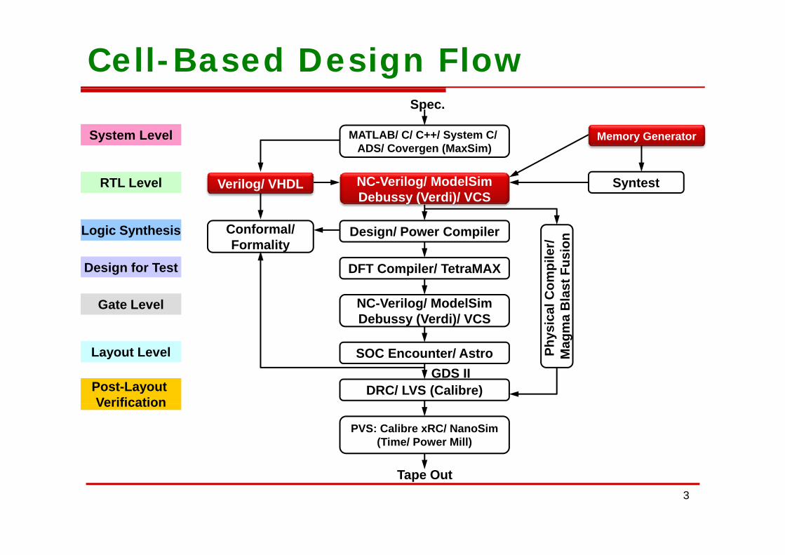
Cell-Based Design Flow
MATLAB/ C/ C++/ System C/ ADS/ Covergen (MaxSim)
Memory Generator
Spec.
System LevelADS/ Covergen (MaxSim)
NC-Verilog/ ModelSimDebussy (Verdi)/ VCS
Verilog/ VHDL SyntestRTL Level
Design/ Power Compiler
DFT Compiler/ TetraMAX
mpi
ler/
Fusi
on
Conformal/Formality
Logic Synthesis
Design for Test
NC-Verilog/ ModelSimDebussy (Verdi)/ VCS
hysi
cal C
omgm
a B
last
Gate Level
SOC Encounter/ Astro
DRC/ LVS (Calibre)
Ph Mag
GDS IILayout Level
Post-Layout Verification
PVS: Calibre xRC/ NanoSim(Time/ Power Mill)
Verification
Tape Out3
Basic Concept of Verilog HDLBasic Concept of Verilog HDL
4
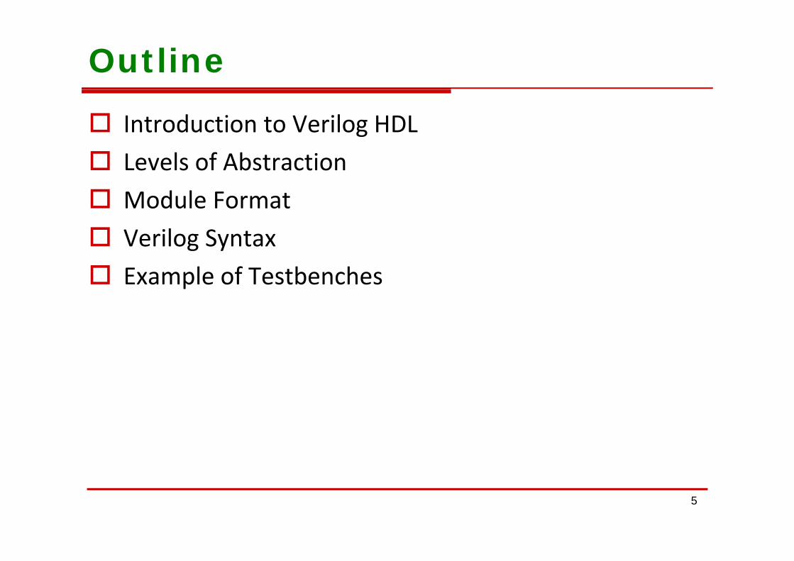
Outline
Introduction to Verilog HDL l f b i Levels of Abstraction Module Format Verilog Syntax Example of Testbenches Example of Testbenches
5
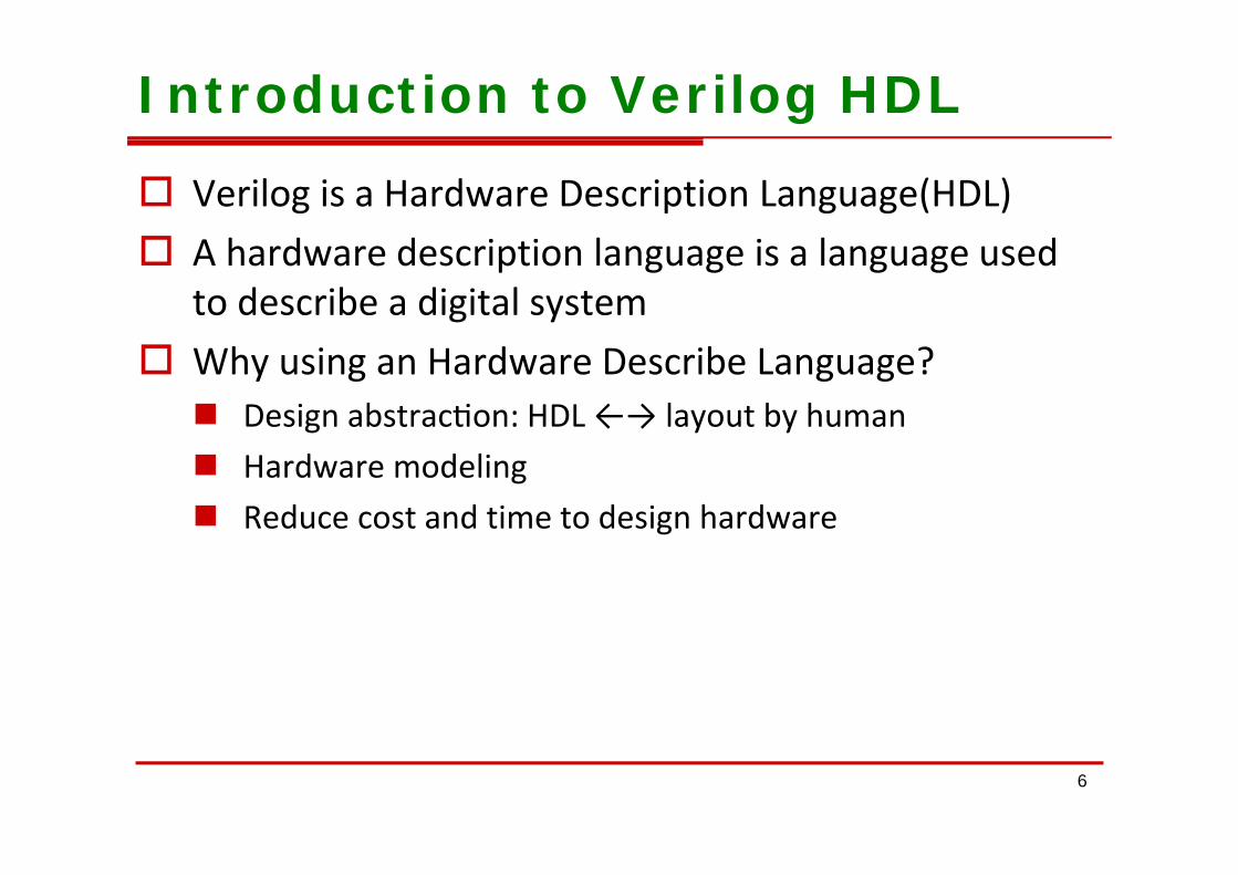
Introduction to Verilog HDL
Verilog is a Hardware Description Language(HDL) h d d i i l i l d A hardware description language is a language used
to describe a digital system Why using an Hardware Describe Language? Design abstrac on: HDL ←→ layout by human Hardware modeling Reduce cost and time to design hardware
6
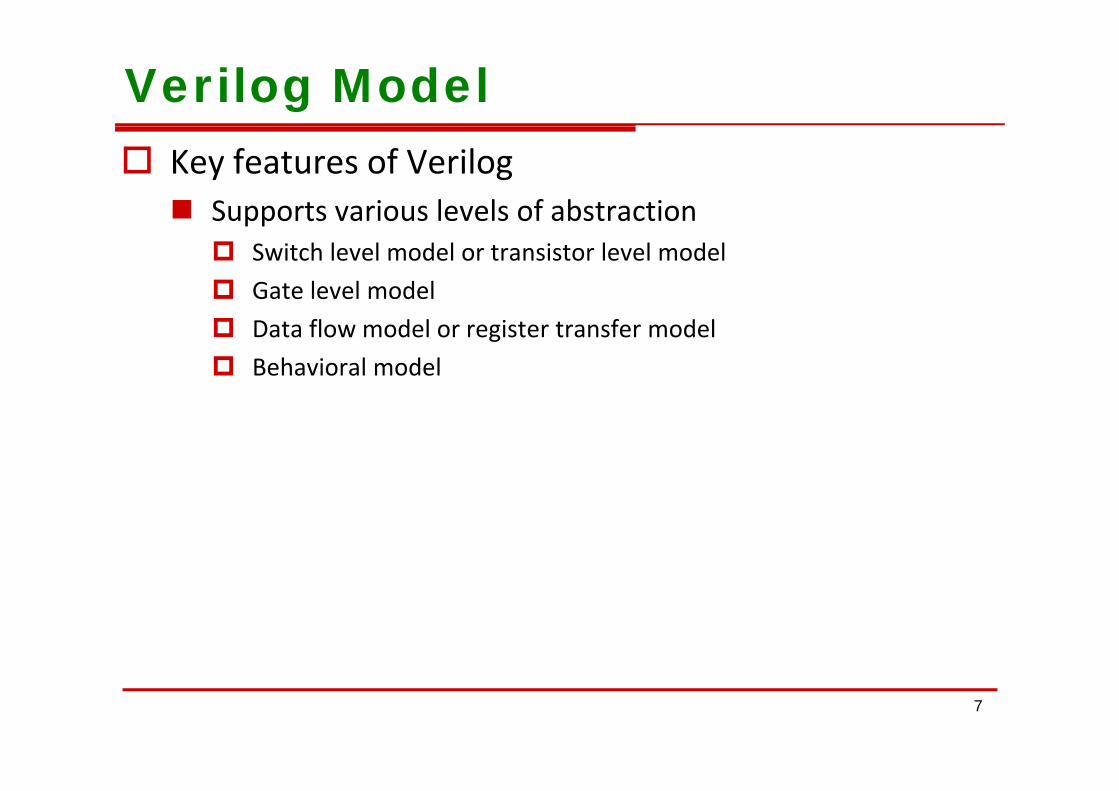
Verilog Model Key features of Verilog Supports various levels of abstraction Supports various levels of abstraction Switch level model or transistor level model Gate level model Data flow model or register transfer model Behavioral model
7

Gate Level Model (GTL) Model consists of basic logic Ex: AND,NAND,OR,NOR,BUF,NOT…etc., , , , ,
//GateAND2module AND2(in1,in2,Out)module AND2(in1,in2,Out)input in1,in2;output Out;
and u1(Out,in1,in2);d d lendmodule
8
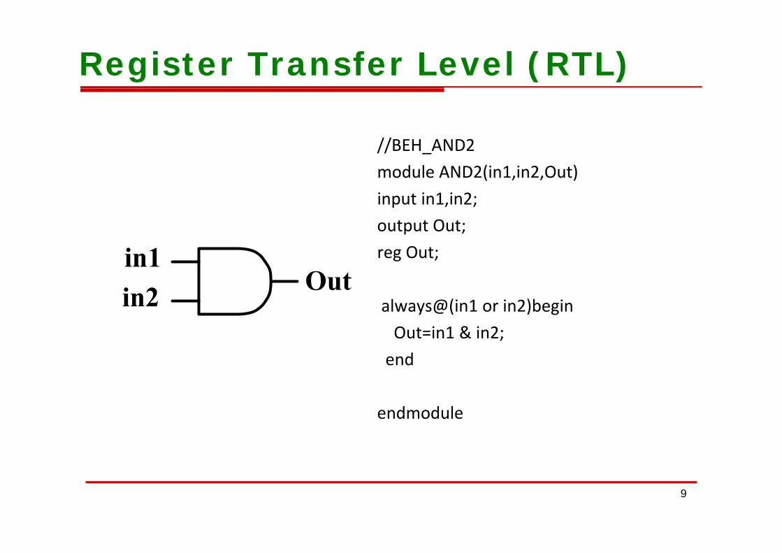
Register Transfer Level (RTL)
//BEH AND2// _module AND2(in1,in2,Out)input in1,in2;output Out;reg Out;
always@(in1 or in2)beginOut=in1 & in2;;end
endmodule
9
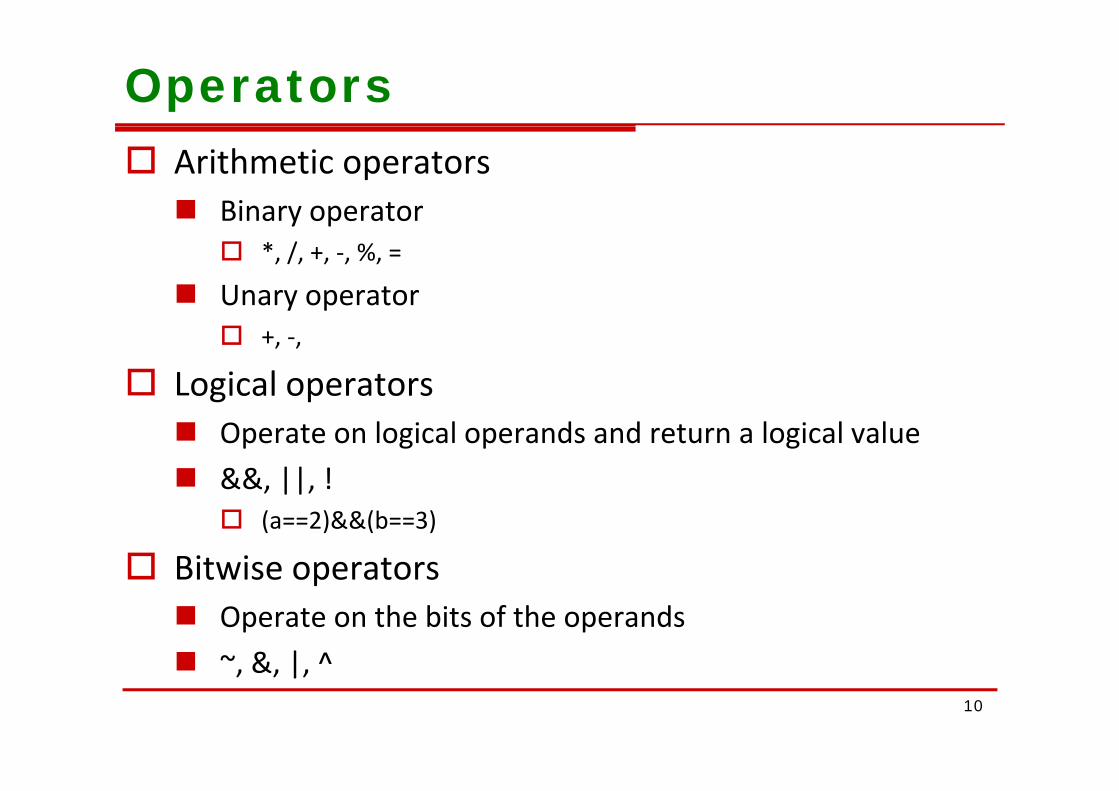
Operators Arithmetic operators Binary operator Binary operator *, /, +, ‐, %, =
Unary operatory p +, ‐,
Logical operatorsogical operators Operate on logical operands and return a logical value && || ! &&, ||, ! (a==2)&&(b==3)
Bitwise operators Bitwise operators Operate on the bits of the operands ~ & | ^ , &, |,
10
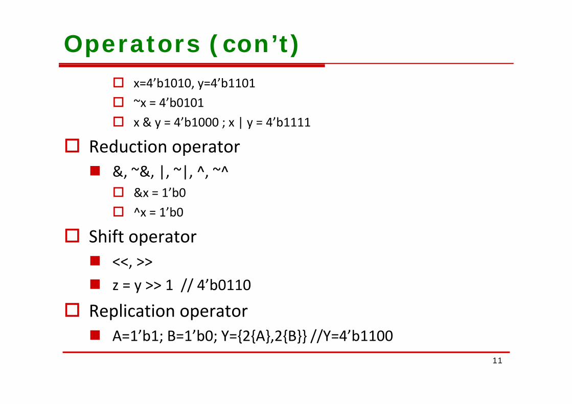
Operators (con’t) x=4’b1010, y=4’b1101 ~x = 4’b0101 x & y = 4’b1000 ; x | y = 4’b1111
Reduction operator &, ~&, |, ~|, ^, ~^ &x = 1’b0 ^x = 1’b0
Shift operator <<, >> z = y >> 1 // 4’b0110
Replication operator A=1’b1; B=1’b0; Y={2{A},2{B}} //Y=4’b1100 A 1 b1; B 1 b0; Y {2{A},2{B}} //Y 4 b1100
11

Verilog Module
Module module test(a,b ,c,d,z,sum);
Module Name &Port List
( )
input a,b; //Inputs to nand gateinput [3:0] c,d; //Bused Input
Port List
DefinitionsPort Wire Register
output z; //Output from nand gateoutput [3:0] sum; //Output from adderwire and_out; //Output from and gate
[3 0] //B d OPort, Wire, RegisterParameter, Integer, Function
Mod le Instantiations
reg [3:0] sum; //Bused Output
And instance1(a,b,and_out);INV i t 2 ( d t )Module Instantiations
Module Statements &
INV instance2 (and_out, z);
always@(c or d)beginsum= c+d;Module Statements &
Constructssum= c+d;
endendmodule
12

Module Format
Basic Verilog description //`i l d & `d fi //`include & `define //module module_name(port list) // i //wire ,reg //logic level description
// //data flow level description // function or task declare // behavioral description block //endmodule
13
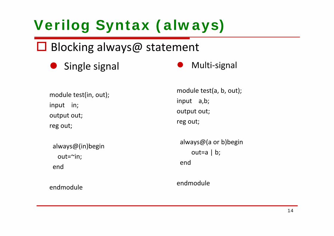
Verilog Syntax (always) Blocking always@ statement Single signal Multi signal Single signal Multi‐signal
module test(a b out);module test(in, out);input in;output out;
module test(a, b, out);input a,b;output out;p ;
reg out;
l @(i )b i
reg out;
always@(a or b)begin always@(in)beginout=~in;
end
y @( ) gout=a | b;
end
endmodule endmodule
14

Verilog Syntax (always) Non‐blocking always@ statement posedge negedge posedge negedge
module test(a, clk, out);input a, clk;output out;
module test(a, clk, out);input a, clk;output out;p ;
reg out;
l @( d lk)b i
p ;reg out;
l @( d lk)b ialways@(posedge clk)beginout = ~ a;end
always@(negedge clk)beginout = ~ a;end
endmodule endmodule
15
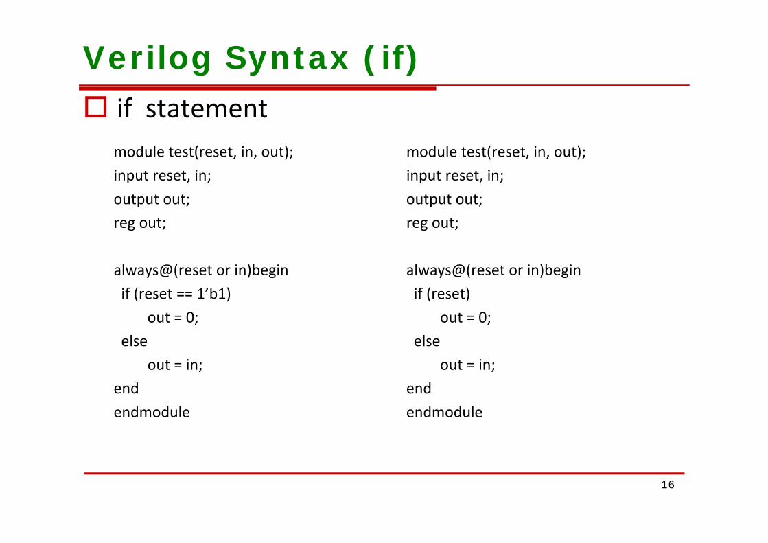
Verilog Syntax (if) if statement
d l t t( t i t) d l t t( t i t)module test(reset, in, out);input reset, in;output out;
module test(reset, in, out);input reset, in;output out;
reg out;
always@(reset or in)begin
reg out;
always@(reset or in)beginalways@(reset or in)beginif (reset == 1’b1)
out = 0;
always@(reset or in)beginif (reset)
out = 0;else
out = in;end
elseout = in;
endendmodule endmodule
16
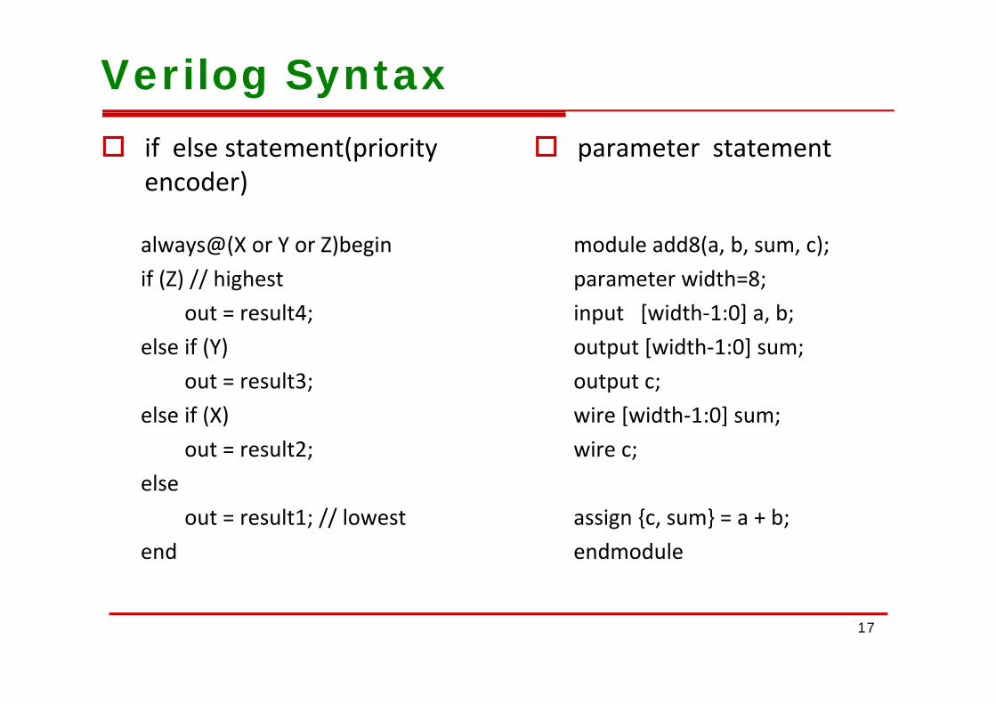
Verilog Syntax if else statement(priority
encoder) parameter statement
)
always@(X or Y or Z)beginif (Z) // hi h
module add8(a, b, sum, c);id h 8if (Z) // highest
out = result4;else if (Y)
parameter width=8;input [width‐1:0] a, b;output [width‐1:0] sum;else if (Y)
out = result3;else if (X)
output [width 1:0] sum;output c;wire [width‐1:0] sum;
out = result2;else
t lt1 // l t
wire c;
i { } bout = result1; // lowestend
assign {c, sum} = a + b;endmodule
17
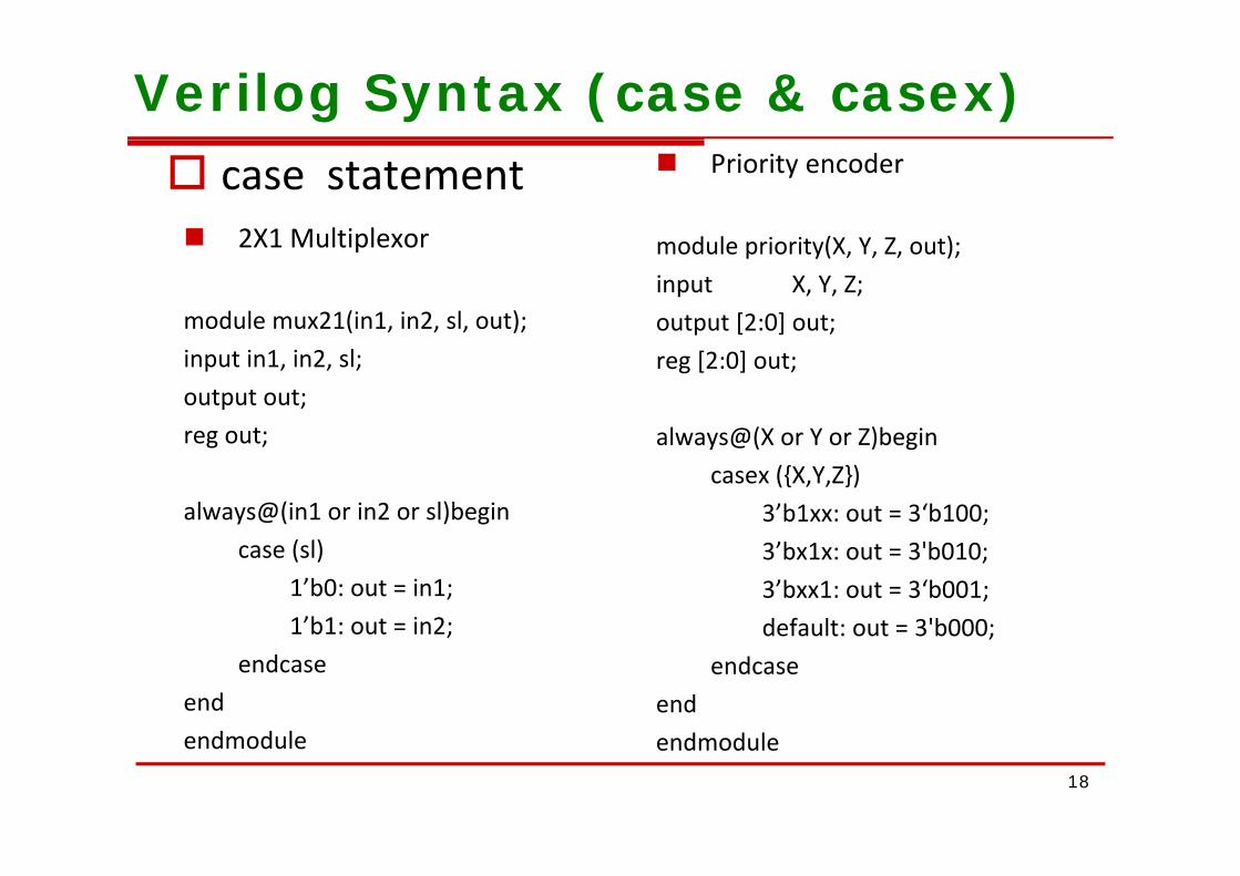
Verilog Syntax (case & casex) case statement 2X1 Multiplexor
Priority encoder
d l i it (X Y Z t) 2X1 Multiplexor
module mux21(in1, in2, sl, out);
module priority(X, Y, Z, out);input X, Y, Z;output [2:0] out;
input in1, in2, sl;output out;reg out;
reg [2:0] out;
always@(X or Y or Z)beginreg out;
always@(in1 or in2 or sl)begin
always@(X or Y or Z)begincasex ({X,Y,Z})
3’b1xx: out = 3‘b100;case (sl)
1’b0: out = in1;1’b1: out = in2;
3’bx1x: out = 3'b010;3’bxx1: out = 3‘b001;default: out = 3'b000;;
endcaseendendmodule
;endcase
endd d l
18
endmodule endmodule

Sequential Logic
Memory Latch Flip‐flopp p Register
Counter Counter Synchronous counter Ripple counter
Finite state machine (FSM) Finite state machine (FSM)
19
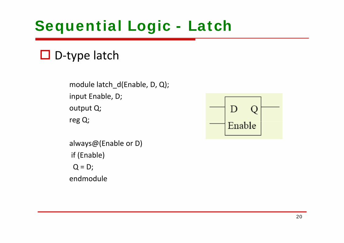
Sequential Logic - Latch
D‐type latch
module latch_d(Enable, D, Q);i E bl Dinput Enable, D;output Q;reg Q;reg Q;
always@(Enable or D)if (Enable)Q = D;d d lendmodule
20
Sequential Logic – Flip Flop
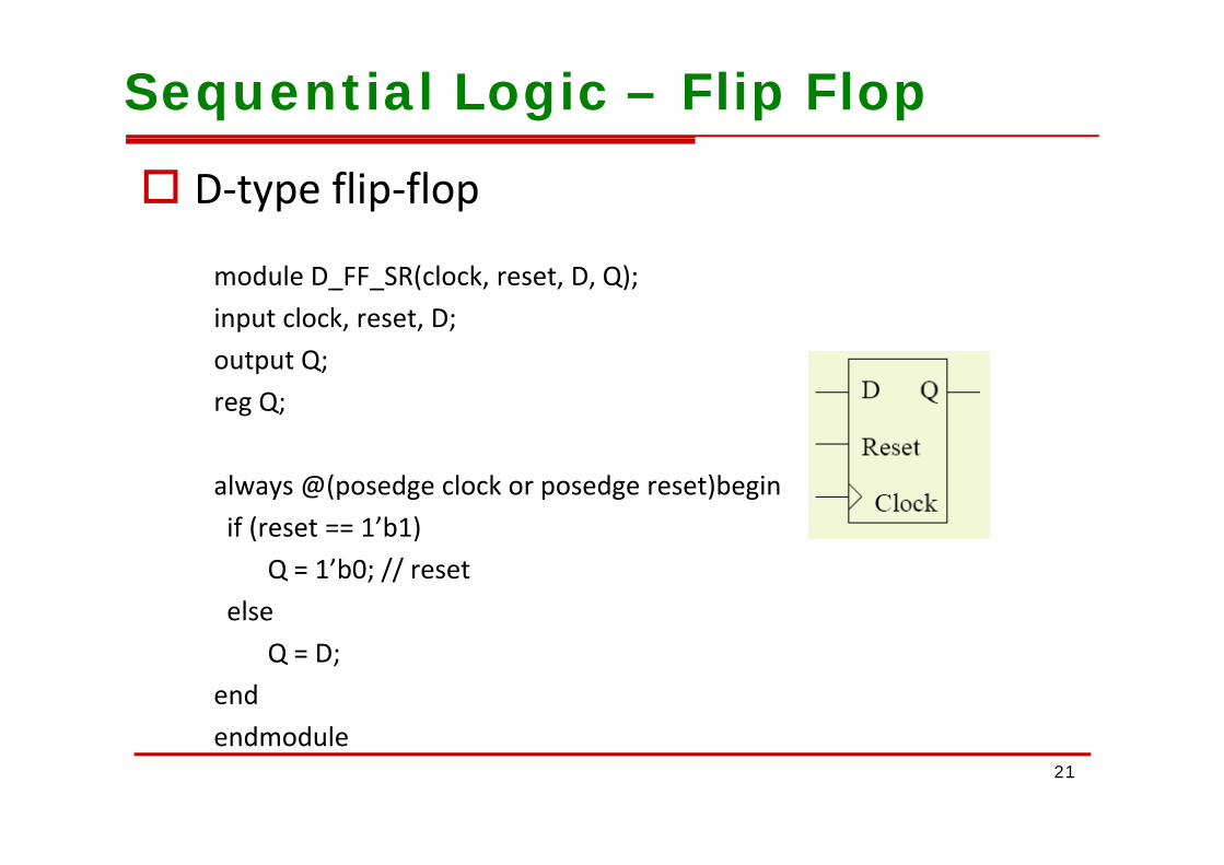
D‐type flip‐flop
module D_FF_SR(clock, reset, D, Q);input clock, reset, D;output Q;reg Q;
always @(posedge clock or posedge reset)beginif (reset == 1’b1)if (reset == 1 b1)
Q = 1’b0; // resetelse
Q = D;end
d d l21
endmodule
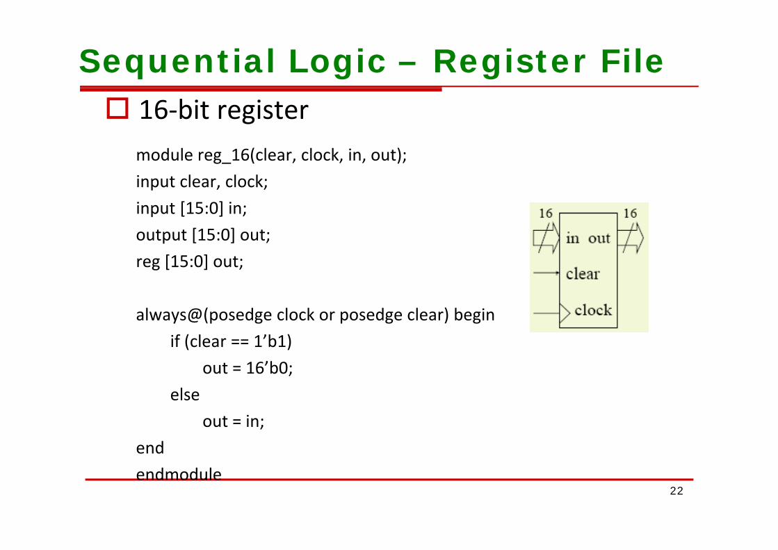
Sequential Logic – Register File 16‐bit register
d l 16( l l k i t)module reg_16(clear, clock, in, out);input clear, clock;input [15:0] in;input [15:0] in;output [15:0] out;reg [15:0] out;
always@(posedge clock or posedge clear) beginif ( l 1’b1)if (clear == 1’b1)
out = 16’b0;elseelse
out = in;end
22endmodule
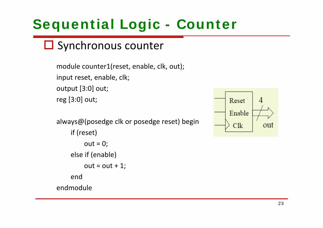
Sequential Logic - Counter Synchronous counter
module counter1(reset, enable, clk, out);input reset, enable, clk;output [3:0] out;output [3:0] out;reg [3:0] out;
always@(posedge clk or posedge reset) beginif (reset)
out = 0;else if (enable)
out = out + 1;out = out + 1;end
endmodule
23
FSM Coding Style
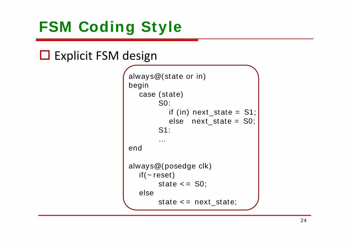
Explicit FSM design always@(state or in)begin
case (state)case (state)S0:
if (in) next_state = S1;else next state = S0;else next_state S0;
S1:…
end
always@(posedge clk)if(~reset)
state <= S0;else
state <= next_state;
24

Example of Testbench
321
25
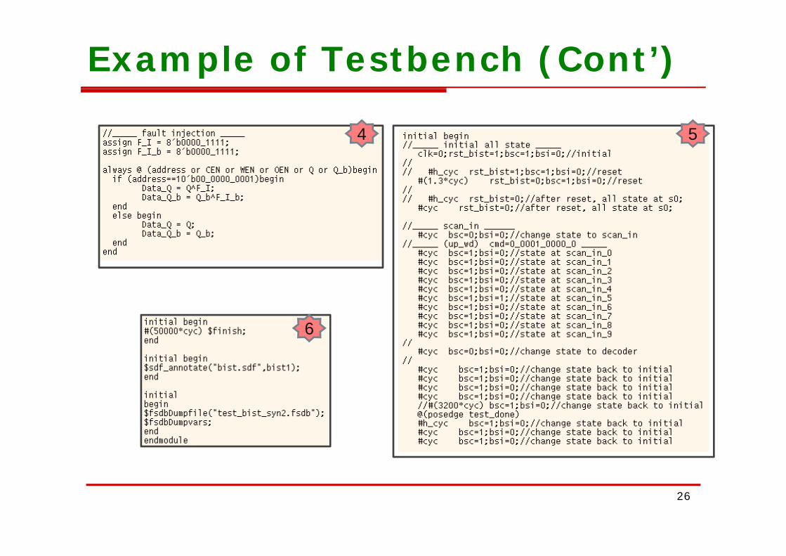
Example of Testbench (Cont’)
4 5
6
26
S th i bl V il C dSynthesizable Verilog Code
27
Synthesizable Verilog Code
Synopsys DO NOT accept all kinds of Verilogd VHDLand VHDL constructs
Synopsys can only accept a subset of Verilogy p y y p gsyntax and this subset is called “Synthesizable Verilog Code”Verilog Code
28
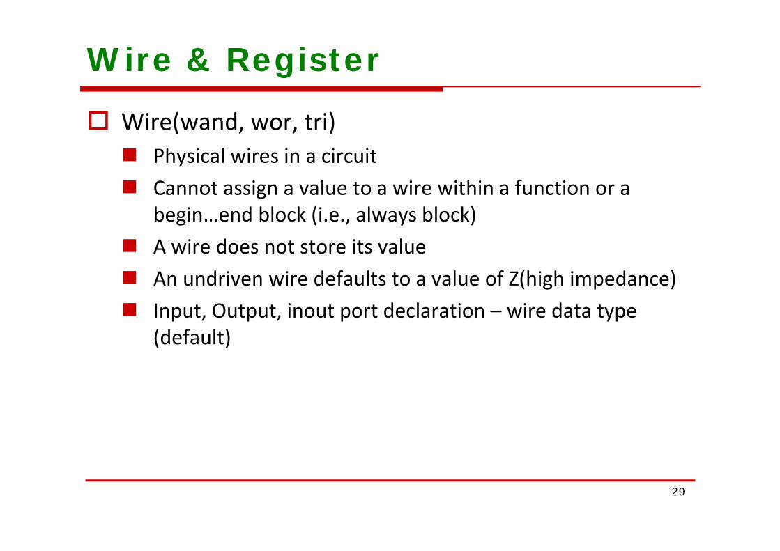
Wire & Register
Wire(wand, wor, tri) Ph i l i i i it Physical wires in a circuit Cannot assign a value to a wire within a function or a
begin end block (i e always block)begin…end block (i.e., always block) A wire does not store its value An undriven wire defaults to a value of Z(high impedance) An undriven wire defaults to a value of Z(high impedance) Input, Output, inout port declaration – wire data type
(default)(default)
29
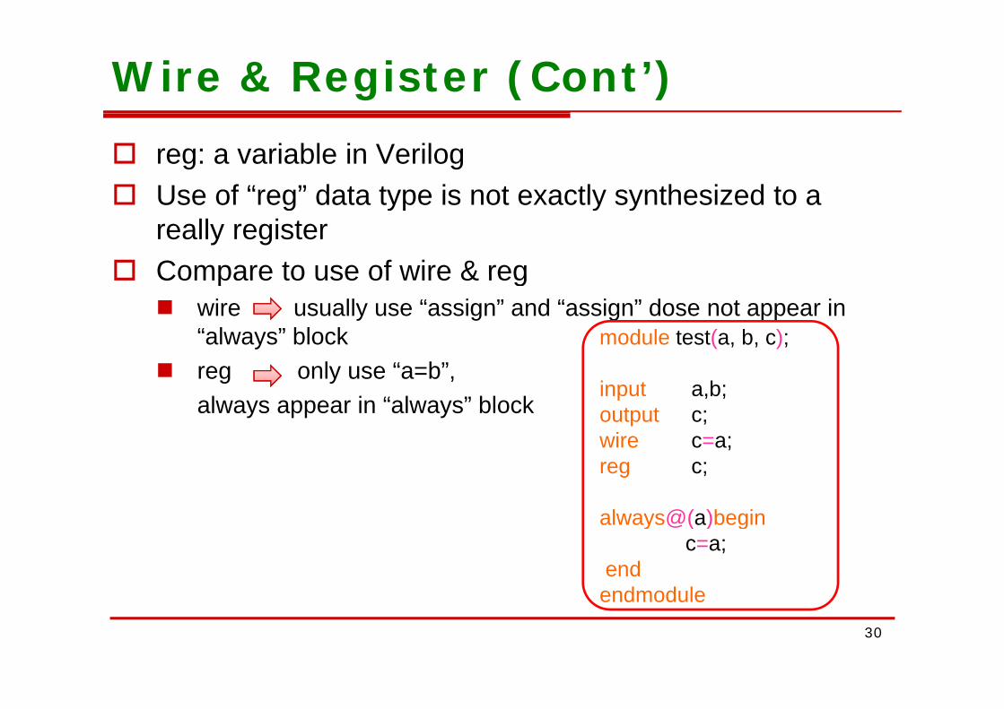
Wire & Register (Cont’) reg: a variable in Verilog Use of “reg” data type is not exactly synthesized to a Use of reg data type is not exactly synthesized to a
really register Compare to use of wire & reg Compare to use of wire & reg
wire usually use “assign” and “assign” dose not appear in “always” block module test(a, b, c);
reg only use “a=b”, always appear in “always” block
input a,b;output c;
iwire c=a;reg c;
always@(a)beginalways@(a)beginc=a;
endendmodule
30
endmodule
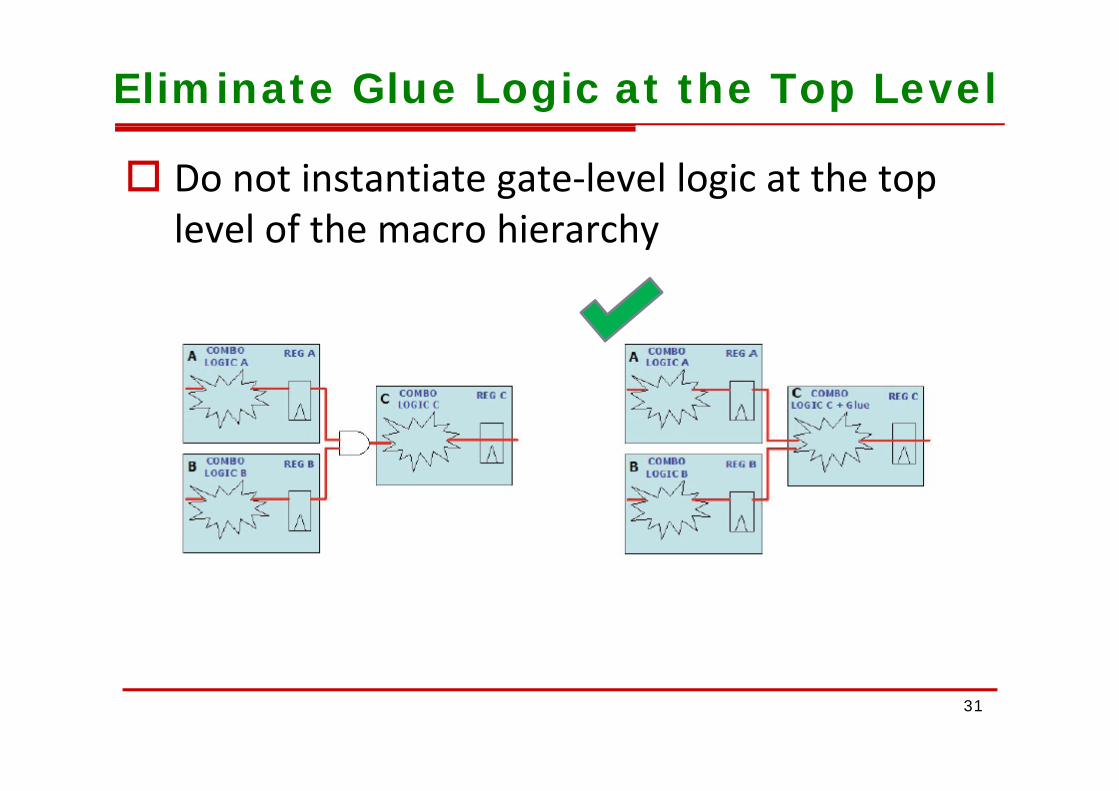
Eliminate Glue Logic at the Top Level
Do not instantiate gate‐level logic at the top l l f h hi hlevel of the macro hierarchy
31
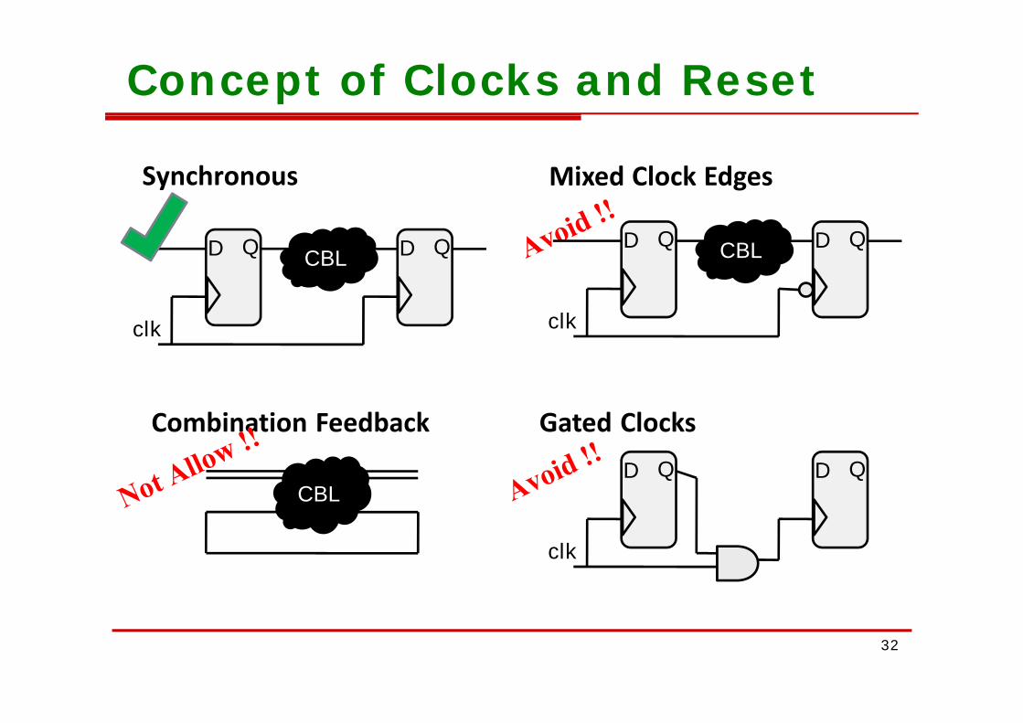
Concept of Clocks and Reset
Synchronous Mixed Clock Edges
QD D QCBLQD D QCBL
clk clk
Gated ClocksCombination FeedbackQD D Q
CBL
clk
32
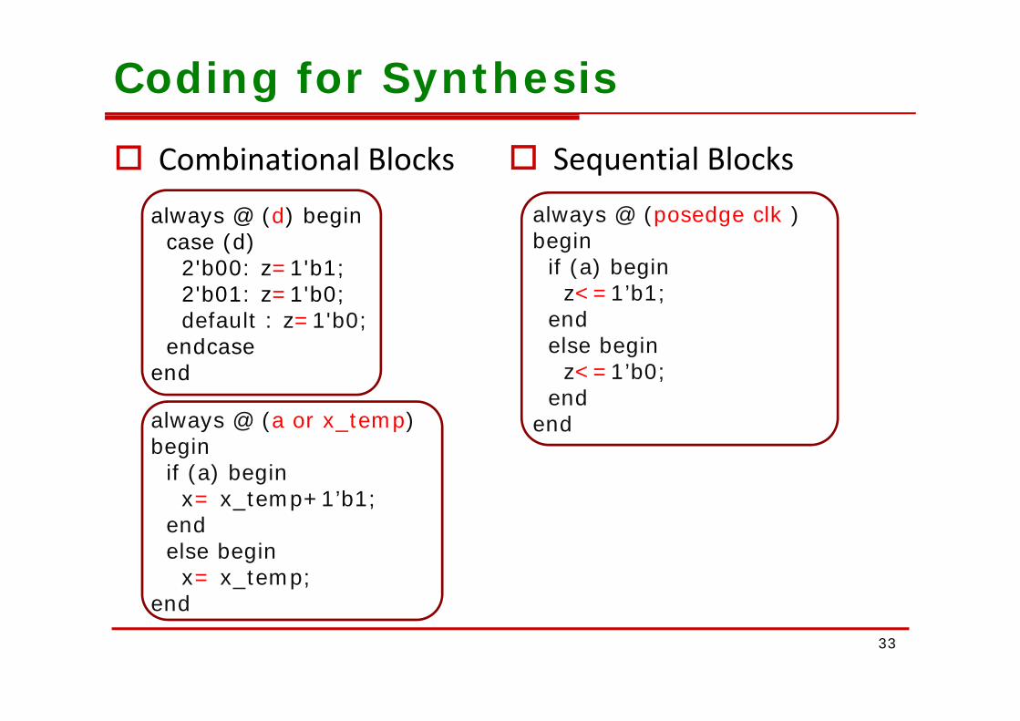
Coding for Synthesis
Combinational Blocks Sequential Blocks
always @ (d) begincase (d)
2'b00: z=1'b1;
always @ (posedge clk ) begin
if (a) begin;2'b01: z=1'b0;default : z=1'b0;
endcase
z<=1’b1;endelse begin
end
always @ (a or x_temp)begin
z<=1’b0;end
endbegin
if (a) beginx= x_temp+1’b1;
endendelse begin
x= x_temp;end
33
end

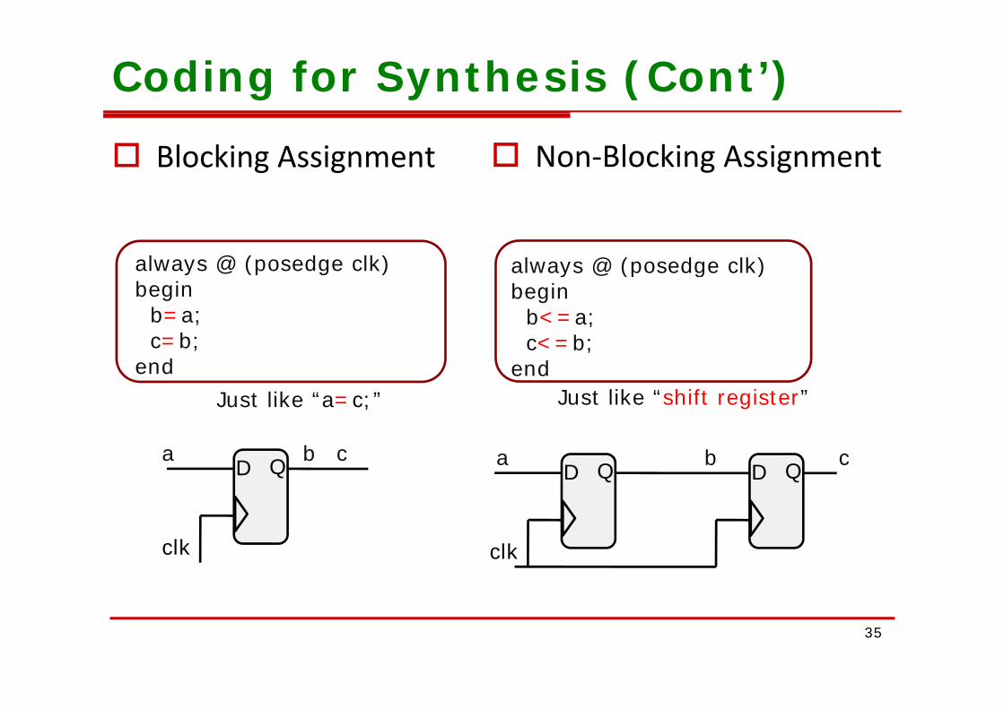
Coding for Synthesis (Cont’)
Avoid Combinational Feedback
l @ ( d lk) b ialways @ (a or x)beginif (a) begin
x= x+1’b1;
always @ (posedge clk) beginx_temp<=x;
endendelse begin
x= x;d
always @ (a or x_temp)beginif (a) begin
x= x temp+1’b1;end x= x_temp+1 b1;endelse begin
x= x temp;x x_temp;end
34
Coding for Synthesis (Cont’)
Blocking Assignment Non‐Blocking Assignment
always @ (posedge clk) always @ (posedge clk) y (p g )begin
b=a;c=b;
y @ (p g )begin
b<=a;c<=b;
end endJust like “a=c;” Just like “shift register”
QD QD D Qa b ca b c
clk clk
35

Coding for Synthesis (Cont’) Avoid Latches
always @ (d) begin1’b0always @ (d) begin
case (d)2'b00: z=1'b1;
x=1’b0;z=1’b0;case (d)
2'b00: begin z 1'b1; x 1’b1; end;
2'b01: z=1'b0;default : z=1'b0;
endcase
2'b00: begin z=1'b1; x=1’b1; end2'b01: begin z=1'b0; enddefault : begin z=1'b0; end
endcaseend
always @ (posedge clk )beginalways @ (d)beginif ( ) b i
endcaseend
if (a) beginz<=1b1;
endl b i
if (a) begin............endelse begin else begin
z<=1’b0;end
end
else begin...........end
end36
endend
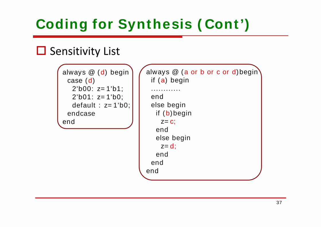
Coding for Synthesis (Cont’)
Sensitivity List
always @ (d) begincase (d)
2'b00: z 1'b1;
always @ (a or b or c or d)beginif (a) begin
2 b00: z=1 b1;2'b01: z=1'b0;default : z=1'b0;
endcase
............endelse begin
if (b)beginendcaseend
if (b)beginz=c;
endelse beginelse begin
z=d;end
endend
37
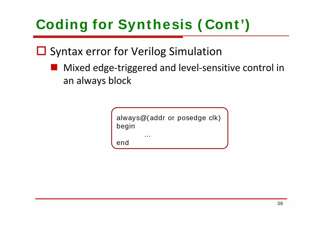
Coding for Synthesis (Cont’)
Syntax error for Verilog Simulation Mixed edge‐triggered and level‐sensitive control in
an always block
always@(addr or posedge clk)begin
…dend
38
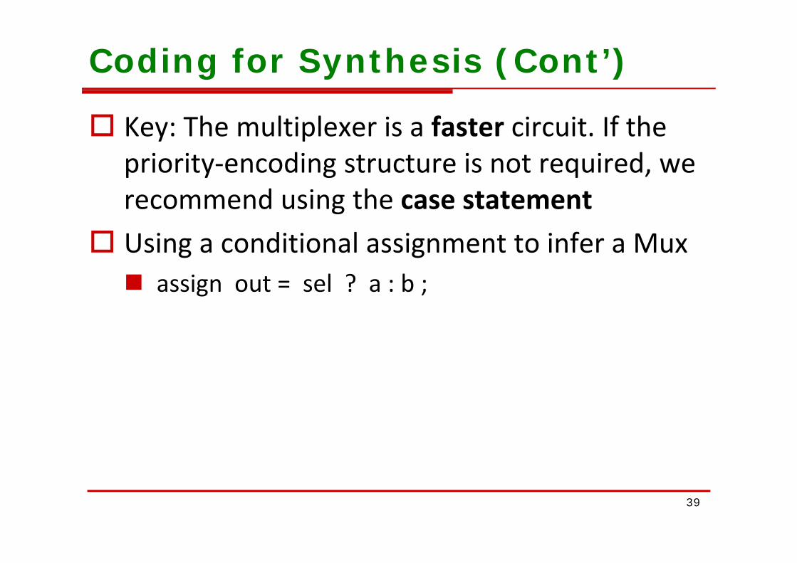
Coding for Synthesis (Cont’)
Key: The multiplexer is a faster circuit. If the i i di i i dpriority‐encoding structure is not required, we
recommend using the case statement Using a conditional assignment to infer a Mux assign out = sel ? a : b ; assign out = sel ? a : b ;
39
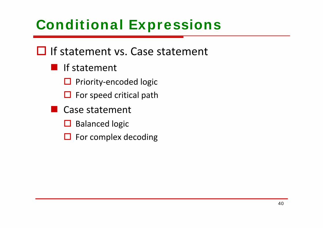
Conditional Expressions
If statement vs. Case statement If statement Priority‐encoded logic For speed critical path
Case statement Balanced logic For complex decodingo co p e decod g
40
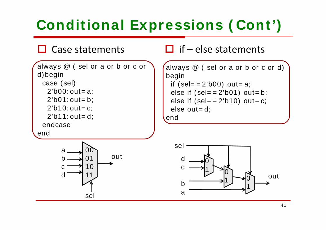
Conditional Expressions (Cont’) Case statements if – else statements
always @ ( sel or a or b or c or d) begin
if (sel==2'b00) out=a;
always @ ( sel or a or b or c or d)begin
case (sel)2'b00 t else if (sel==2'b01) out=b;
else if (sel==2'b10) out=c;else out=d;d
2'b00:out=a;2'b01:out=b;2'b10:out=c;2'b11:out d; end2'b11:out=d;
endcaseend
abc
out000110
01
dc
sel
cd
l
1011 0
1
01
1c
ba
out
41
sel a
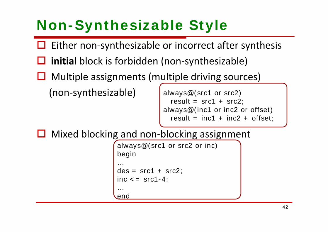
Non-Synthesizable Style Either non‐synthesizable or incorrect after synthesis initial block is forbidden (non‐synthesizable) initial block is forbidden (non synthesizable) Multiple assignments (multiple driving sources)
( th i bl )(non‐synthesizable) always@(src1 or src2)result = src1 + src2;
always@(inc1 or inc2 or offset)lt i 1 i 2 ff t
Mixed blocking and non‐blocking assignmentresult = inc1 + inc2 + offset;
always@(src1 or src2 or inc)begin…d 1 2des = src1 + src2;inc <= src1-4;…end
42
end
Tips for Verilog Design
Resource Sharing Scalable Design Using ( ) to describe complex circuits Using ( ) to describe complex circuits Timescale
43
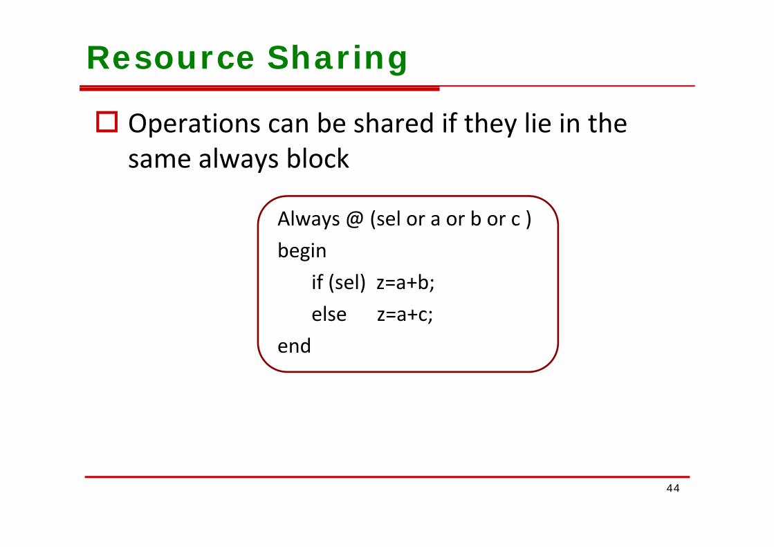
Resource Sharing
Operations can be shared if they lie in the l bl k
Al @ ( l b )
same always block
Always @ (sel or a or b or c )begin
if (sel) z=a+b;else z=a+c;
end
44

Scalable Design
parameter size=8;[ ] b dwire [3:0] a,b,c,d,e;
assign a=size+2;assign b=a+1;
ConstantIncreaserAddassign c=d+e; Adder
45

Omit for Synthesis
Omit the Wait for XX ns Statement Do not use “#XX;”
Omit the ...After XX ns or Delay Statement Omit the ...After XX ns or Delay Statement Do not use “assign #XX Q=0;”
O i I i i l V l Omit Initial Values Do not use “initial sum = 1’b0;”
46
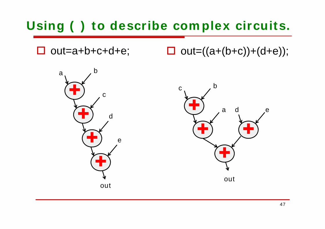
Using ( ) to describe complex circuits.
out=a+b+c+d+e; out=((a+(b+c))+(d+e));
a b
c bc
d
c
a d ed
ee
outout
47
Timescale `timescale: which declares the time unit and precision.
`timescale <time unit> / <time precision>_ / _p e.g. : `timescale 1s/1ps, to advance 1 sec, the timewheel scans its
queues 1012 times versus a `timescale 1s/1ms, where it only scans the queues 103 timesthe queues 103 times.
The time_precision must be at least as precise as the time unittime_unit
Keep precision as close in scale to the time units as is practicalp
If not specified, the simulator may assign a default timescale unit
The smallest precision of all the timescale directive determines the “simulation time unit ” of the simulation.
48
Summary No initial in the RTL code FFs are preferred FFs are preferred Avoid unnecessary latches Avoid combinational feedback For sequential blocks, use no‐blocking statements For combinational blocks, use blocking statements Coding state machines Coding state machines Two procedure blocks: one for the sequential and one for the
combinationalcombinational Keep FSM logic and non‐FSM logic in separate modules Assign a default state Assign a default state
49
Artisan Memory CompilerArtisan Memory Compiler
50
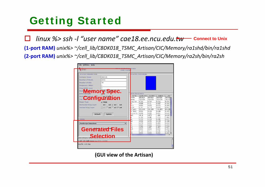
Getting Started linux %> ssh ‐l “user name” cae18.ee.ncu.edu.tw(1‐port RAM) unix%> ~/cell_lib/CBDK018_TSMC_Artisan/CIC/Memory/ra1shd/bin/ra1shd
Connect to Unix
(2‐port RAM) unix%> ~/cell_lib/CBDK018_TSMC_Artisan/CIC/Memory/ra2sh/bin/ra2sh
Memory Spec.y pConfiguration
Generated FilesSelectionSelection
(GUI view of the Artisan)( )
51
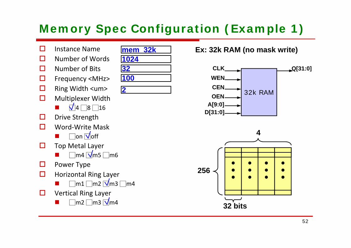
Memory Spec Configuration (Example 1) Instance Name Number of Words Number of Bits
Ex: 32k RAM (no mask write)mem_32k102432 CLK Q[31:0] Number of Bits
Frequency <MHz> Ring Width <um> l l d h
321002 32k RAM
CLKWENCENOEN
Q[31:0]
Multiplexer Width □4 □8 □16
Drive Strength
OENA[9:0]
D[31:0]
Word‐Write Mask □on □off
Top Metal Layer
4
□m4 □m5 □m6 Power Type Horizontal Ring Layer 256
□m1 □m2 □m3 □m4 Vertical Ring Layer
□m2 □m3 □m4 32 bits3 b ts
52

Memory Spec Configuration (Example 2) Instance Name Number of Words Number of Bits
Ex: 64k RAM (with mask write)mem_64k204832 CLK Q[31:0] Number of Bits
Frequency <MHz> Ring Width <um> Multiplexer Width
321002 64k RAM
CLKWEN[3:0]
CENOEN
Q[31:0]
p □4 □8 □16
Drive Strength Word‐Write Mask
OENA[9:0]
D[31:0]
□on □off Word Partition Size
Top Metal Layer □m4□m5□m6
88
□m4 □m5 □m6 Power Type Horizontal Ring Layer
□m1 □m2 □m3 □m4256
□ □ □ □
Vertical Ring Layer □m2 □m3 □m4
32 bits3 b ts
53
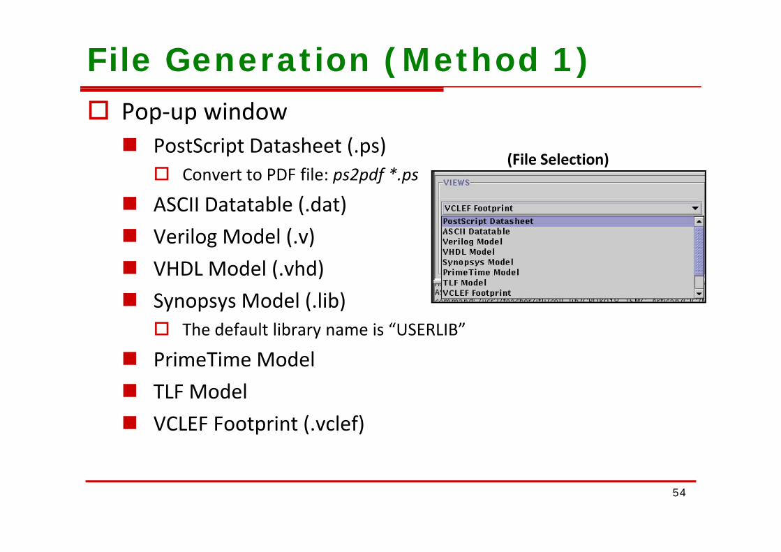
File Generation (Method 1) Pop‐up window PostScript Datasheet (.ps) PostScript Datasheet (.ps) Convert to PDF file: ps2pdf *.ps
ASCII Datatable (.dat)
(File Selection)
( ) Verilog Model (.v) VHDL Model (.vhd)( ) Synopsys Model (.lib) The default library name is “USERLIB”
PrimeTime Model TLF Model VCLEF Footprint (.vclef)
54
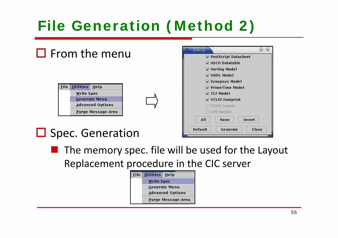
File Generation (Method 2)
From the menu
Spec. Generationh f l ll b d f h The memory spec. file will be used for the Layout Replacement procedure in the CIC server
55

Simulation and Debugging ToolsSimulation and Debugging Tools
56
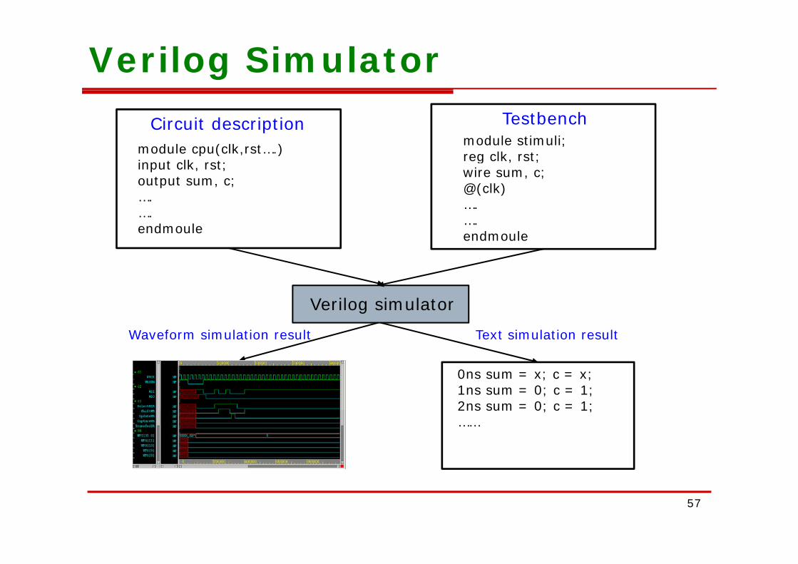
Verilog SimulatorCircuit description
module cpu(clk,rst….)
Testbenchmodule stimuli;reg clk rst;p ( , )
input clk, rst;output sum, c;….….
reg clk, rst;wire sum, c;@(clk)….
endmoule ….endmoule
Verilog simulator
Text simulation resultWaveform simulation result
0ns sum = x; c = x;1ns sum = 0; c = 1;2ns sum = 0; c = 1;2ns sum 0; c 1;……
57

Verilog-XL & NC-Verilog Verilog-XL > il fil 1 fil 2 t tb h > verilog filename1.v filename2.v … testbench.v
NC-Verilog > ncverilog +access+rwc filename1.v filename2.v …
No syntax error 1 Syntax error!y y
58
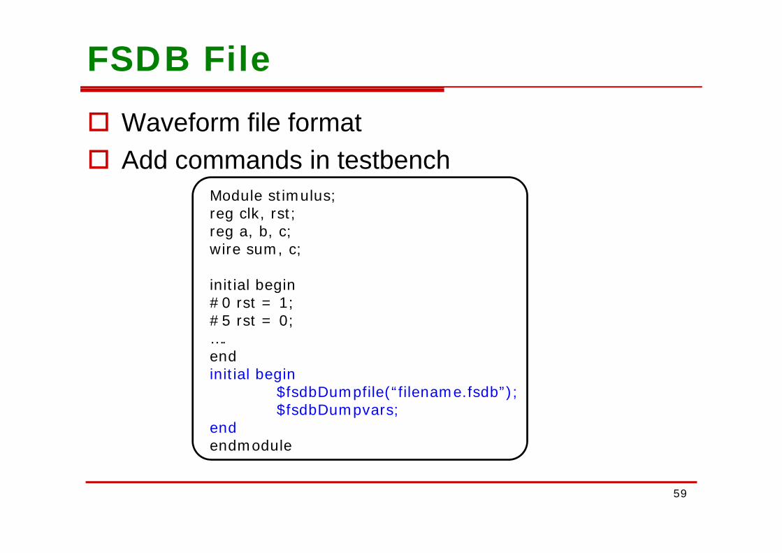
FSDB File Waveform file format Add d i t tb h Add commands in testbench
Module stimulus;reg clk rst;reg clk, rst;reg a, b, c;wire sum, c;
initial begin#0 rst = 1;#5 rst = 0;….endinitial begin
$fsdbDumpfile(“filename.fsdb”);$fsdbDumpvars;
endendmodule
59

Debussy – Getting Start nWave – waveform viewer > W > nWave
60
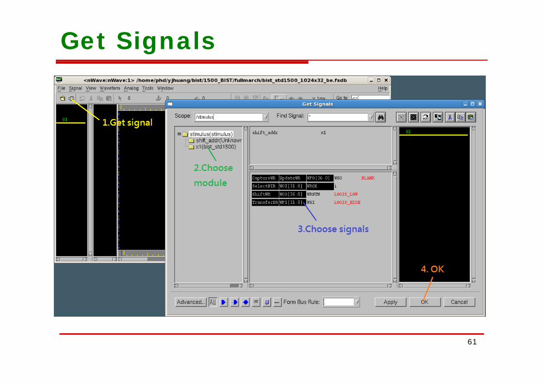
Get Signals
61
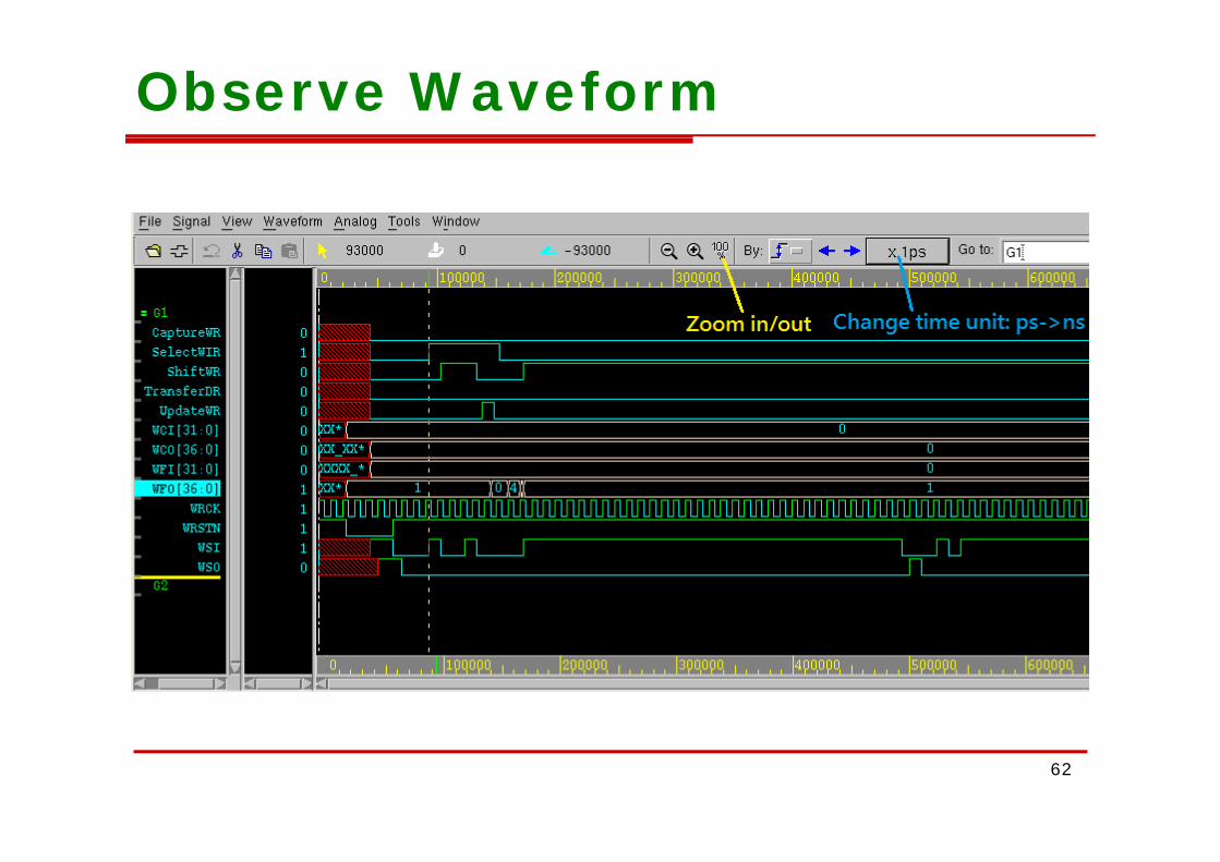
Observe Waveform
62
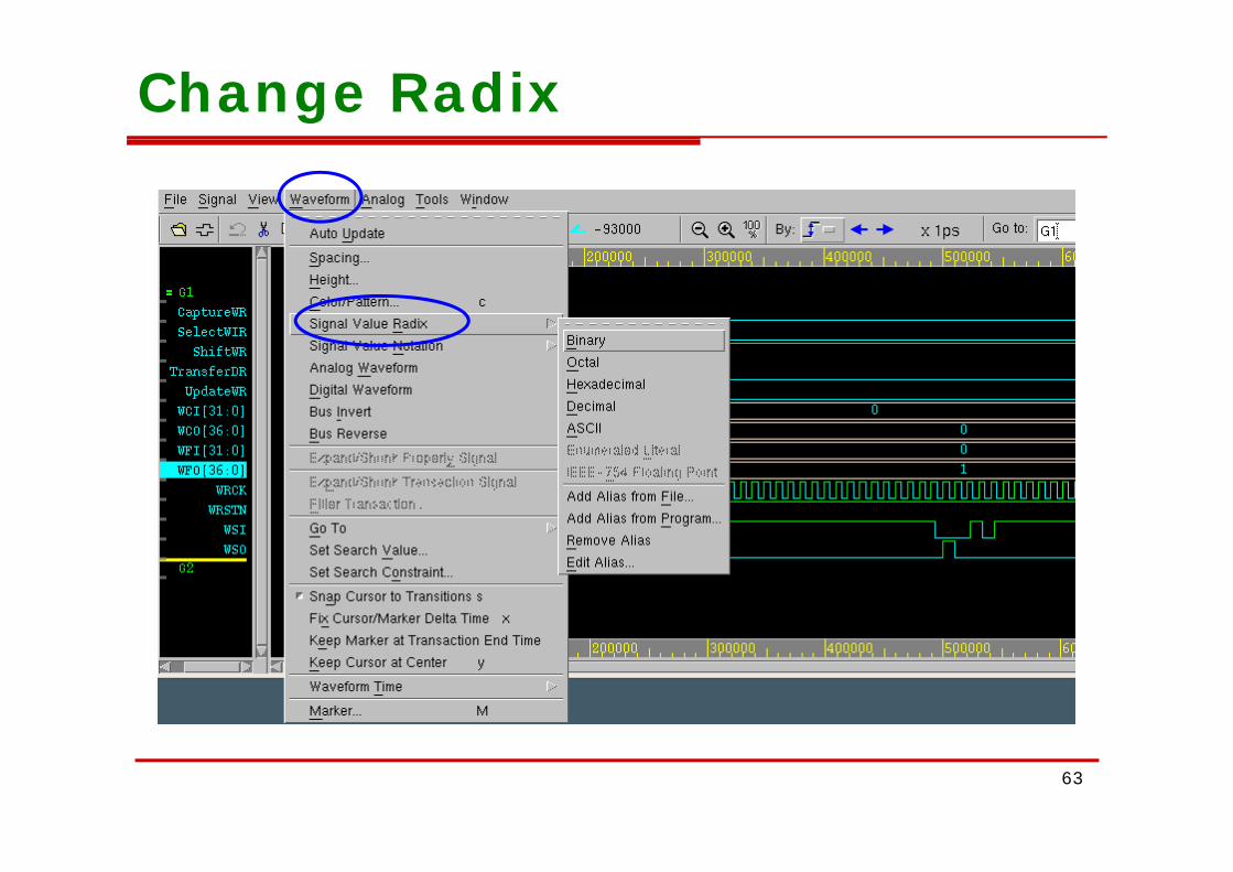
Change Radix
63
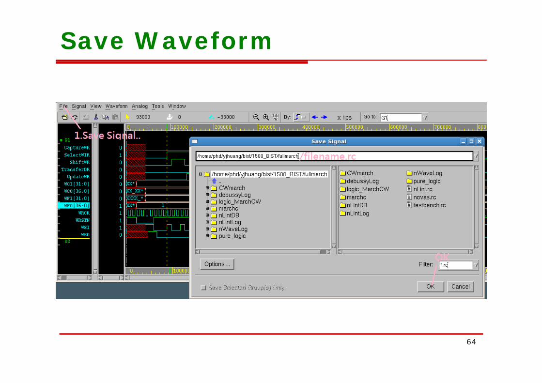
Save Waveform
64