Embed Size (px)
Citation preview
Revision HistoryThe following table shows the revision history for this document.
Section Revision Summary07/14/2020 Version 2020.1
Initial release N/A
Revision History
UG1273 (v2020.1) July 14, 2020 www.xilinx.comVersal ACAP Design Guide 2Send Feedback
Table of ContentsRevision History...............................................................................................................2
Chapter 1: Overview......................................................................................................5Introduction to Versal ACAP.......................................................................................................5Navigating Content by Design Process.................................................................................... 6About This Guide......................................................................................................................... 7
Chapter 2: System Architecture............................................................................. 8AI Engine...................................................................................................................................... 9Programmable Logic................................................................................................................ 10NoC..............................................................................................................................................11XPIO............................................................................................................................................ 11DDRMC........................................................................................................................................12CIPS............................................................................................................................................. 12GT................................................................................................................................................ 18HSDP........................................................................................................................................... 18
Chapter 3: System Methodology..........................................................................19System Design Methodology...................................................................................................19System Simulation Methodology............................................................................................ 27System Debug Methodology................................................................................................... 28
Chapter 4: Design Flow.............................................................................................. 31Vitis Environment Design Flow................................................................................................ 31Vivado Tools Design Flow......................................................................................................... 39Simulation Flows....................................................................................................................... 47Boot and Configuration............................................................................................................49
Chapter 5: System Migration................................................................................. 51Soft Memory Controllers.......................................................................................................... 52GT................................................................................................................................................ 53AXI Interconnect........................................................................................................................53Power and Error Handling....................................................................................................... 53
UG1273 (v2020.1) July 14, 2020 www.xilinx.comVersal ACAP Design Guide 3Send Feedback
System Monitor......................................................................................................................... 54DSP.............................................................................................................................................. 54On-Chip Memory Resources.................................................................................................... 55CLB.............................................................................................................................................. 55System Debug............................................................................................................................55Processor and Peripherals....................................................................................................... 57I/O............................................................................................................................................... 57PCIe Subsystems....................................................................................................................... 57Security....................................................................................................................................... 59PL Configuration and JTAG....................................................................................................... 59
Appendix A: Primitives.............................................................................................. 61RAM Primitives...........................................................................................................................61DSP Primitives............................................................................................................................66CLB Primitives............................................................................................................................ 70
Appendix B: Additional Resources and Legal Notices............................. 73Xilinx Resources.........................................................................................................................73Documentation Navigator and Design Hubs.........................................................................73References..................................................................................................................................73Please Read: Important Legal Notices................................................................................... 75
UG1273 (v2020.1) July 14, 2020 www.xilinx.comVersal ACAP Design Guide 4Send Feedback
Chapter 1
Overview
Introduction to Versal ACAPVersal™ adaptive compute acceleration platforms (ACAPs) combine Scalar Engines, AdaptableEngines, and Intelligent Engines with leading-edge memory and interfacing technologies todeliver powerful heterogeneous acceleration for any application. Most importantly, Versal ACAPhardware and software are targeted for programming and optimization by data scientists andsoftware and hardware developers. Versal ACAPs are enabled by a host of tools, software,libraries, IP, middleware, and frameworks to enable all industry-standard design flows.
Built on the TSMC 7 nm FinFET process technology, the Versal portfolio is the first platform tocombine software programmability and domain-specific hardware acceleration with theadaptability necessary to meet today's rapid pace of innovation. The portfolio includes six seriesof devices uniquely architected to deliver scalability and AI inference capabilities for a host ofapplications across different markets—from cloud—to networking—to wireless communications—to edge computing and endpoints.
The Versal architecture combines different engine types with a wealth of connectivity andcommunication capability and a network on chip (NoC) to enable seamless memory-mappedaccess to the full height and width of the device. Intelligent Engines are SIMD VLIW AI Enginesfor adaptive inference and advanced signal processing compute, and DSP Engines for fixed point,floating point, and complex MAC operations. Adaptable Engines are a combination ofprogrammable logic blocks and memory, architected for high-compute density. Scalar Engines,including Arm® Cortex™-A72 and Cortex-R5F processors, allow for intensive compute tasks.
The Versal AI Core series delivers breakthrough AI inference acceleration with AI Engines thatdeliver over 100x greater compute performance than current server-class of CPUs. This series isdesigned for a breadth of applications, including cloud for dynamic workloads and network formassive bandwidth, all while delivering advanced safety and security features. AI and datascientists, as well as software and hardware developers, can all take advantage of the high-compute density to accelerate the performance of any application.
Chapter 1: Overview
UG1273 (v2020.1) July 14, 2020 www.xilinx.comVersal ACAP Design Guide 5Send Feedback
The Versal Prime series is the foundation and the mid-range of the Versal platform, serving thebroadest range of uses across multiple markets. These applications include 100G to 200Gnetworking equipment, network and storage acceleration in the Data Center, communicationstest equipment, broadcast, and aerospace & defense. The series integrates mainstream 58Gtransceivers and optimized I/O and DDR connectivity, achieving low-latency acceleration andperformance across diverse workloads.
The Versal Premium series provides breakthrough heterogeneous integration, very high-performance compute, connectivity, and security in an adaptable platform with a minimizedpower and area footprint. The series is designed to exceed the demands of high-bandwidth,compute-intensive applications in wired communications, data center, test & measurement, andother applications. Versal Premium series ACAPs include 112G PAM4 transceivers and integratedblocks for 600G Ethernet, 600G Interlaken, PCI Express® Gen5, and high-speed cryptography.
The Versal architecture documentation suite is available at: https://www.xilinx.com/versal.
Navigating Content by Design ProcessXilinx® documentation is organized around a set of standard design processes to help you findrelevant content for your current development task. This document covers the following designprocesses:
• System and Solution Planning: Identifying the components, performance, I/O, and datatransfer requirements at a system level. Includes application mapping for the solution to PS,PL, and AI Engine. Topics in this document that apply to this design process include:
• Chapter 2: System Architecture
• Chapter 3: System Methodology
• Chapter 4: Design Flow
• Chapter 5: System Migration
• Embedded Software Development: Creating the software platform from the hardwareplatform and developing the application code using the embedded CPU. Also covers XRT andGraph APIs. Topics in this document that apply to this design process include:
• Vitis Environment Design Flow
• Simulation Flows
• Host Software Development: Developing the application code, accelerator development,including library, XRT, and Graph API use. Topics in this document that apply to this designprocess include:
• Vitis Environment Design Flow
Chapter 1: Overview
UG1273 (v2020.1) July 14, 2020 www.xilinx.comVersal ACAP Design Guide 6Send Feedback
• Simulation Flows
• AI Engine Development: Creating the AI Engine graph and kernels, library use, simulationdebugging and profiling, and algorithm development. Also includes the integration of the PLand AI Engine kernels. Topics in this document that apply to this design process include:
• AI Engine
• Vitis Environment Design Flow
• Hardware, IP, and Platform Development: Creating the PL IP blocks for the hardwareplatform, creating PL kernels, subsystem functional simulation, and evaluating the Vivado®
timing, resource use, and power closure. Also involves developing the hardware platform forsystem integration. Topics in this document that apply to this design process include:
• Vivado Tools Design Flow
• Simulation Flows
• System Integration and Validation: Integrating and validating the system functionalperformance, including timing, resource use, and power closure. Topics in this document thatapply to this design process include:
• System Simulation Methodology
• System Debug Methodology
• Chapter 4: Design Flow
About This GuideThis guide provides a high-level overview of the Versal ACAP as follows:
• Chapter 2: System Architecture: Provides an overview of the Versal ACAP with a summary ofeach high-level integrated block, including the purpose of each block and how blocks arerelated to each other.
• Chapter 3: System Methodology: Provides high-level methodology recommendations.
• Chapter 4: Design Flow: Describes the Xilinx design tools and supported design flowsavailable for Versal ACAPs.
• Chapter 5: System Migration: Provides high-level system migration recommendations as wellas block-by-block migration information for designs targeting the Versal ACAP.
• Appendix A: Primitives: Provides information on Versal ACAP primitives.
Chapter 1: Overview
UG1273 (v2020.1) July 14, 2020 www.xilinx.comVersal ACAP Design Guide 7Send Feedback
Chapter 2
System ArchitectureThe Xilinx® Versal™ ACAP is a collection of programmable resources that work together to forma system on chip (SoC). Following are the major resource blocks:
• AI Engine
Note: AI Engine availability is device specific.
• Programmable logic (PL)
• Network on chip (NoC)
• High-speed I/O (XPIO)
• Integrated memory controllers LPDDR4 and DDR4 (DDRMC)
• Processing system (PS)
• Platform management controller (PMC)
• Integrated block for PCIe® with DMA and cache coherent interconnect (CPM)
Note: CPM availability is device specific.
• Transceivers (GT)
• High-speed debug port (HSDP)
Versal ACAP applications can exploit the capabilities of each of these resources. To create ormigrate a design to a Versal ACAP, you must identify which resources best satisfy the differentneeds of the application and partition the application across those resources.
The following figure shows the layout of the Versal ACAP.
Chapter 2: System Architecture
UG1273 (v2020.1) July 14, 2020 www.xilinx.comVersal ACAP Design Guide 8Send Feedback
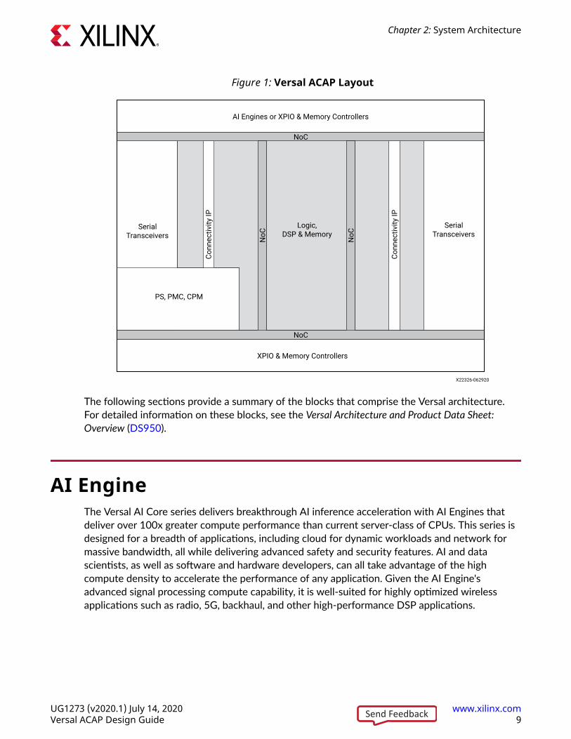
Figure 1: Versal ACAP Layout
AI Engines or XPIO & Memory Controllers
XPIO & Memory Controllers
SerialTransceivers
PS, PMC, CPM
SerialTransceivers
Logic,DSP & Memory
NoC
NoC
NoC
NoC
Conn
ectiv
ity IP
Conn
ectiv
ity IP
X22326-062920
The following sections provide a summary of the blocks that comprise the Versal architecture.For detailed information on these blocks, see the Versal Architecture and Product Data Sheet:Overview (DS950).
AI EngineThe Versal AI Core series delivers breakthrough AI inference acceleration with AI Engines thatdeliver over 100x greater compute performance than current server-class of CPUs. This series isdesigned for a breadth of applications, including cloud for dynamic workloads and network formassive bandwidth, all while delivering advanced safety and security features. AI and datascientists, as well as software and hardware developers, can all take advantage of the highcompute density to accelerate the performance of any application. Given the AI Engine'sadvanced signal processing compute capability, it is well-suited for highly optimized wirelessapplications such as radio, 5G, backhaul, and other high-performance DSP applications.
Chapter 2: System Architecture
UG1273 (v2020.1) July 14, 2020 www.xilinx.comVersal ACAP Design Guide 9Send Feedback
AI Engines are an array of very-long instruction word (VLIW) processors with single instructionmultiple data (SIMD) vector units that are highly optimized for compute-intensive applications,specifically digital signal processing (DSP), 5G wireless applications, and artificial intelligence (AI)technology such as machine learning (ML).
AI Engines provide multiple levels of parallelism including instruction-level and data-levelparallelism. Instruction-level parallelism includes a scalar operation, up to two moves, two vectorreads (loads), one vector write (store), and one vector instruction that can be executed—in total, a7-way VLIW instruction per clock cycle. Data-level parallelism is achieved via vector-leveloperations where multiple sets of data can be operated on a per-clock-cycle basis. Each AIEngine contains both a vector and scalar processor, dedicated program memory, local 32 KB datamemory, access to local memory in any of three neighboring directions. It also has access toDMA engines and AXI4 interconnect switches to communicate via streams to other AI Engines orto the programmable logic (PL) or the DMA. Refer to the Versal ACAP AI Engine ArchitectureManual (AM009) for specific details on the AI Engine array and interfaces.
Programmable LogicThe Versal ACAP programmable logic (PL) comprises configurable logic blocks (CLBs), internalmemory, and DSP engines. Every CLB contains 64 flip-flops and 32 look-up tables (LUTs). Half ofthe CLB LUTs can be configured as a 64-bit RAM, as a 32-bit shift register (SRL32), or as two 16-bit shift registers (SRL16). In addition to the LUTs and flip-flops, the CLB contains the following:
• Carry lookahead logic for implementing arithmetic functions or wide logic functions
• Dedicated, internal connections to create fast LUT cascades without external routing
This enables a flexible carry logic structure that allows a carry chain to start at any bit in thechain. In addition to the distributed RAM (64-bit each) capability in the CLB, there are dedicatedblocks for optimally building memory arrays in the design:
• Accelerator RAM (4MB) (available in some Versal devices only)
• Block RAM (36 Kb each) where each port can be configured as 4Kx9, 2Kx18, 1Kx36, or512x72 in simple dual-port mode
• UltraRAM (288 Kb each) where each port can be configured as 32Kx9, 16Kx18, 8Kx36, or4Kx72
Versal devices also include many low-power DSP Engines, combining high speed with small sizewhile retaining system design flexibility. The DSP engines can be configured in various modes tobetter match the application needs:
• 27×24-bit twos complement multiplier and a 58-bit accumulator
• Three element vector/INT8 dot product
Chapter 2: System Architecture
UG1273 (v2020.1) July 14, 2020 www.xilinx.comVersal ACAP Design Guide 10Send Feedback
• Complex 18bx18b multiplier
• Single precision floating point
For more information on PL resources, see the Versal ACAP Configurable Logic Block ArchitectureManual (AM005), Versal ACAP Memory Resources Architecture Manual (AM007), and Versal ACAPDSP Engine Architecture Manual (AM004).
NoCThe NoC is a high-speed communication subsystem that transfers data between intellectualproperty (IP) Endpoints in the PL, PS, and other integrated blocks, providing unified intra-dieconnectivity. The NoC master and slave interfaces can be configured as AXI3, AXI4, or AXI4-Stream. The NoC converts these AXI interfaces to a 128-bit wide NoC packet protocol thatmoves data horizontally and vertically across the device via the HNoC and VNoC respectively.The HNoC runs at the bottom and top of the Versal ACAP, close to the I/O banks and integratedblocks (e.g., processors, memory controllers, PCIe interfaces). The number of VNoCs (up to 8)depends on the device and the amount of DDRMCs (up to 4 DDRMCs). For more information onthe AXI protocol, see the Vivado Design Suite: AXI Reference Guide (UG1037).
The Versal ACAP NoC IP acts as the logical representation of the Versal ACAP NoC. The NoCmain function is to efficiently move data between the DDR controllers and the rest of the device.The Versal ACAP NoC IP enables multiple masters to access a shared DDRMC with advancedquality of service (QoS) settings. The AXI NoC IP is required to connect the PS or the PL to theDDRMC. The AXI NoC IP can also be used to create additional connections between the PS andthe PL or between design modules located in the PL.
For more information on the NoC IP and performance, see the Versal ACAP ProgrammableNetwork on Chip and Integrated Memory Controller LogiCORE IP Product Guide (PG313).
XPIOThe XPIO in Versal ACAPs are similar to the high-speed I/O (HPIO) in the UltraScale™architecture. However, the XPIO are located at the bottom and/or top periphery of the device,unlike the I/O columnar layout in previous devices. The XPIO provide XPHY logic that is similarto UltraScale device native mode. The XPHY logic encapsulates calibrated delays along withserialization and deserialization logic for 6 single-ended I/O ports known as nibble. Each XPIObank contains 9 XPHY logic sites and supports up to 54 single-ended I/O ports. The XPHY logicis used for the integrated DDRMC, soft memory controllers, and custom high-performance I/Ointerfaces. For more information on the XPIO, see the Versal ACAP SelectIO Resources ArchitectureManual (AM010).
Chapter 2: System Architecture
UG1273 (v2020.1) July 14, 2020 www.xilinx.comVersal ACAP Design Guide 11Send Feedback
DDRMCThe DDRMC is a high-efficiency, low-latency integrated DDR controller for a variety ofapplications, including general purpose central processing units (CPUs) as well as other traditionalfield programmable gate array (FPGA) applications, such as video or network buffering.
The controller operates at half the DRAM clock frequency and supports DDR4, LPDDR4, andLPDDR4X standards up to 4266 Mb/s. The controller can be configured as a single DDRinterface with data widths of 16, 32, and 64 bits, plus an extra 8 check bits when error-correctioncode (ECC) is enabled. The controller can also be configured as 2 independent or interleavedDDR interfaces of 16 or 32 data bits each. The controller supports x4, x8, and x16 DDR4 andx32 LPDDR4 components, small outline dual in-line memory modules (SODIMMs), unbufferedDIMMs (UDIMMs), registered DIMMs (RDIMMs), and load-reduced DIMMs (LRDIMMs). TheDDRMC is accessed through the NoC.
In Versal ACAP, the DDRMC is a system-wide, shared resource. It is shared between the PS andPL via the device-wide, high-performance NoC interface. The NoC IP core can be configured toinclude one or more integrated DDRMCs. If two or four DDRMCs are selected, the DDRMCs aregrouped to form a single interleaved memory. In interleaved mode, the application views theparticipating DDRMCs as a single unified block of memory. The NoC supports interleaving acrosstwo or four DDRMCs by automatically dividing AXI requests into interleaved, block-sizedsubrequests and alternately sending the subrequests to each of the participating DDRMCs.
Note: You must use the NoC to connect between the PL, PS, CPM, or AI Engine and the DDRMC.
For more information on the DDRMC, see the Network on Chip and Integrated Memory Controllerv1.0 LogiCORE IP Product Guide (PG313).
Note: Versal ACAP also supports soft memory controllers in the PL fabric, similar to previous devicefamilies.
CIPSThe PS, PMC, and CPM modules are grouped together and configured using the Control,Interface, and Processing System (CIPS) IP core as shown in the following figure.
Note: The Versal ACAP includes multiple power domains in the PS, PL and PMC. In the PS, the RPU is inthe in the low-power domain (LPD), and the APU is in the full-power domain (FPD). There are twoimplementations of the CPM depending on the target device capability: CPM4 that is compliant with thePCIe Base Specification Revision 4.0 and CPM5 that is compliant with the PCIe Base Specification Revision5.0. CPM4 is fully powered by the PL domain while CPM5 is powered by its own dedicated supply(VCCINT_CPM) as well as the PS LPD.
Chapter 2: System Architecture
UG1273 (v2020.1) July 14, 2020 www.xilinx.comVersal ACAP Design Guide 12Send Feedback
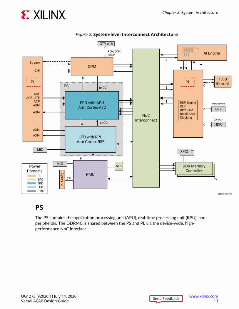
Figure 2: System-level Interconnect Architecture
FPD with APUArm Cortex-A72
LPD with RPUArm Cortex-R5F
HDIO
100G Ethernet
to CCI
to CCI
GTY x16
PCIe/CCIXHSDP
GTs
XPIO
DDR MemoryController
PS
AI Engine
NPI
NoCInterconnect LVCMOS
ACEACE_LITE
ACPAXI4
AXI4
AXI4
AXI4
PMCCFI
PL C
onfig
Stream
CHI
Transceivers
CPM
DSP EngineCLBUltraRAMBlock RAMClocking
PLSPDFPDLPDPMC
Power Domains
MIO
MIO
PLPL
X21692-041720
PSThe PS contains the application processing unit (APU), real-time processing unit (RPU), andperipherals. The DDRMC is shared between the PS and PL via the device-wide, high-performance NoC interface.
Chapter 2: System Architecture
UG1273 (v2020.1) July 14, 2020 www.xilinx.comVersal ACAP Design Guide 13Send Feedback
APU
The Versal ACAP APU includes a dual-core Arm® Cortex™-A72 processor attached to a 1 MBunified L2 cache. The APU is designed for system control and compute-intensive applicationsthat do not need real-time performance. The increased performance of Versal ACAP requireshigher performance from the memory subsystem. To help meet these requirements, the VersalACAP includes an increased L1 instruction cache size (32 KB to 48 KB) as well as multipleDDRMCs and the NoC, which improve the performance of the main memory.
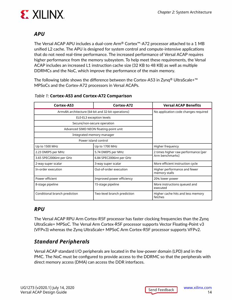
The following table shows the difference between the Cortex-A53 in Zynq® UltraScale+™MPSoCs and the Cortex-A72 processors in Versal ACAPs.
Table 1: Cortex-A53 and Cortex-A72 Comparison
Cortex-A53 Cortex-A72 Versal ACAP BenefitsArmv8A architecture (64-bit and 32-bit operations) No application code changes required
EL0-EL3 exception levels
Secure/non-secure operation
Advanced SIMD NEON floating-point unit
Integrated memory manager
Power island control
Up to 1500 MHz Up to 1700 MHz Higher frequency
2.23 DMIPS per MHz 5.74 DMIPS per MHz 2 times higher raw performance (perArm benchmarks)
3.65 SPEC2006int per GHz 6.84 SPEC2006int per GHz
2-way super scalar 3-way super scalar More efficient instruction cycle
In-order execution Out-of-order execution Higher performance and fewermemory stalls
Power efficient Improved power efficiency 20% lower power
8-stage pipeline 15-stage pipeline More instructions queued andexecuted
Conditional branch prediction Two-level branch prediction Higher cache hits and less memoryfetches
RPU
The Versal ACAP RPU Arm Cortex-R5F processor has faster clocking frequencies than the ZynqUltraScale+ MPSoC. The Versal Arm Cortex-R5F processor supports Vector Floating-Point v3(VFPv3) whereas the Zynq UltraScale+ MPSoC Arm Cortex-R5F processor supports VFPv2.
Standard Peripherals
Versal ACAP standard I/O peripherals are located in the low-power domain (LPD) and in thePMC. The NoC must be configured to provide access to the DDRMC so that the peripherals withdirect memory access (DMA) can access the DDR interfaces.
Chapter 2: System Architecture
UG1273 (v2020.1) July 14, 2020 www.xilinx.comVersal ACAP Design Guide 14Send Feedback
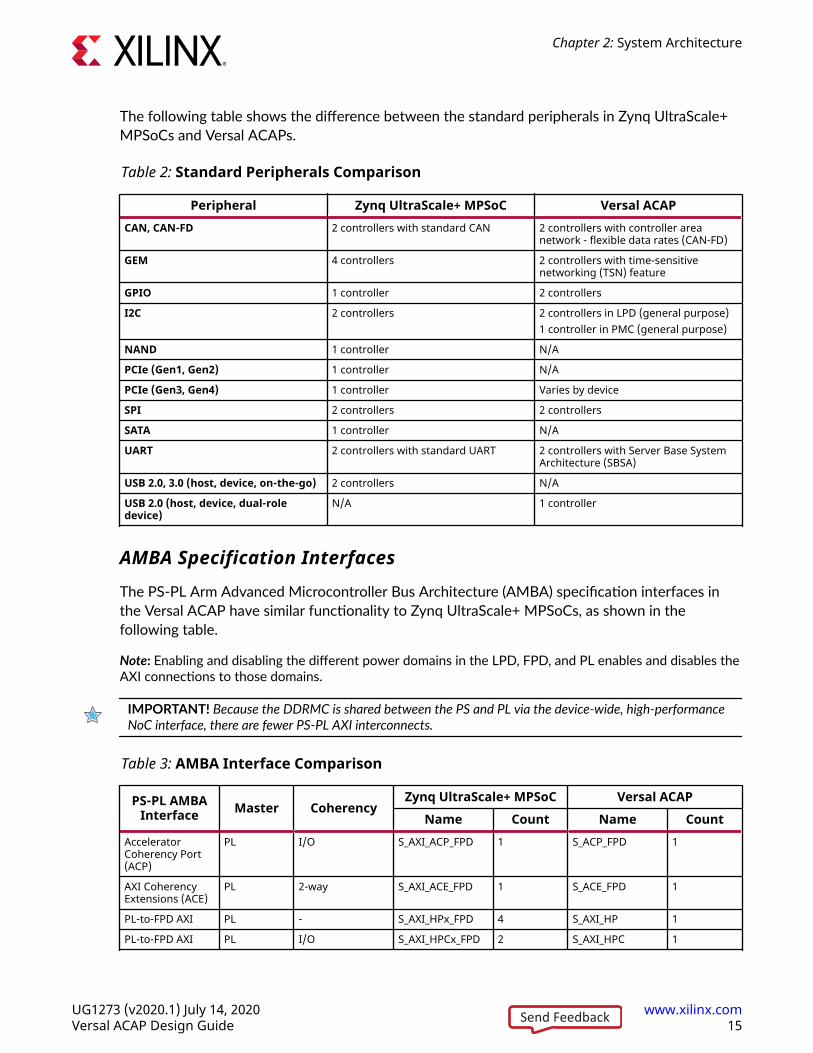
The following table shows the difference between the standard peripherals in Zynq UltraScale+MPSoCs and Versal ACAPs.
Table 2: Standard Peripherals Comparison
Peripheral Zynq UltraScale+ MPSoC Versal ACAPCAN, CAN-FD 2 controllers with standard CAN 2 controllers with controller area
network - flexible data rates (CAN-FD)
GEM 4 controllers 2 controllers with time-sensitivenetworking (TSN) feature
GPIO 1 controller 2 controllers
I2C 2 controllers 2 controllers in LPD (general purpose)1 controller in PMC (general purpose)
NAND 1 controller N/A
PCIe (Gen1, Gen2) 1 controller N/A
PCIe (Gen3, Gen4) 1 controller Varies by device
SPI 2 controllers 2 controllers
SATA 1 controller N/A
UART 2 controllers with standard UART 2 controllers with Server Base SystemArchitecture (SBSA)
USB 2.0, 3.0 (host, device, on-the-go) 2 controllers N/A
USB 2.0 (host, device, dual-roledevice)
N/A 1 controller
AMBA Specification Interfaces
The PS-PL Arm Advanced Microcontroller Bus Architecture (AMBA) specification interfaces inthe Versal ACAP have similar functionality to Zynq UltraScale+ MPSoCs, as shown in thefollowing table.
Note: Enabling and disabling the different power domains in the LPD, FPD, and PL enables and disables theAXI connections to those domains.
IMPORTANT! Because the DDRMC is shared between the PS and PL via the device-wide, high-performanceNoC interface, there are fewer PS-PL AXI interconnects.
Table 3: AMBA Interface Comparison
PS-PL AMBAInterface Master Coherency
Zynq UltraScale+ MPSoC Versal ACAPName Count Name Count
AcceleratorCoherency Port(ACP)
PL I/O S_AXI_ACP_FPD 1 S_ACP_FPD 1
AXI CoherencyExtensions (ACE)
PL 2-way S_AXI_ACE_FPD 1 S_ACE_FPD 1
PL-to-FPD AXI PL - S_AXI_HPx_FPD 4 S_AXI_HP 1
PL-to-FPD AXI PL I/O S_AXI_HPCx_FPD 2 S_AXI_HPC 1
Chapter 2: System Architecture
UG1273 (v2020.1) July 14, 2020 www.xilinx.comVersal ACAP Design Guide 15Send Feedback
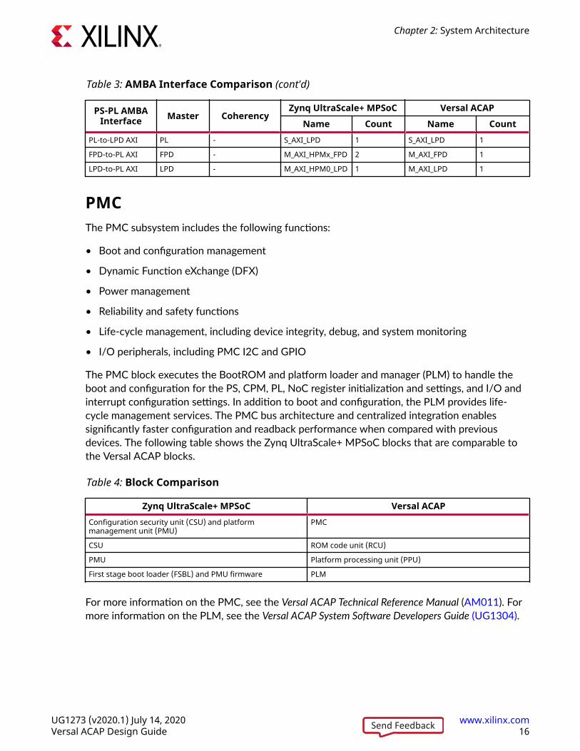
Table 3: AMBA Interface Comparison (cont'd)
PS-PL AMBAInterface Master Coherency
Zynq UltraScale+ MPSoC Versal ACAPName Count Name Count
PL-to-LPD AXI PL - S_AXI_LPD 1 S_AXI_LPD 1
FPD-to-PL AXI FPD - M_AXI_HPMx_FPD 2 M_AXI_FPD 1
LPD-to-PL AXI LPD - M_AXI_HPM0_LPD 1 M_AXI_LPD 1
PMCThe PMC subsystem includes the following functions:
• Boot and configuration management
• Dynamic Function eXchange (DFX)
• Power management
• Reliability and safety functions
• Life-cycle management, including device integrity, debug, and system monitoring
• I/O peripherals, including PMC I2C and GPIO
The PMC block executes the BootROM and platform loader and manager (PLM) to handle theboot and configuration for the PS, CPM, PL, NoC register initialization and settings, and I/O andinterrupt configuration settings. In addition to boot and configuration, the PLM provides life-cycle management services. The PMC bus architecture and centralized integration enablessignificantly faster configuration and readback performance when compared with previousdevices. The following table shows the Zynq UltraScale+ MPSoC blocks that are comparable tothe Versal ACAP blocks.
Table 4: Block Comparison
Zynq UltraScale+ MPSoC Versal ACAPConfiguration security unit (CSU) and platformmanagement unit (PMU)
PMC
CSU ROM code unit (RCU)
PMU Platform processing unit (PPU)
First stage boot loader (FSBL) and PMU firmware PLM
For more information on the PMC, see the Versal ACAP Technical Reference Manual (AM011). Formore information on the PLM, see the Versal ACAP System Software Developers Guide (UG1304).
Chapter 2: System Architecture
UG1273 (v2020.1) July 14, 2020 www.xilinx.comVersal ACAP Design Guide 16Send Feedback
Flash Memory Controllers
The PMC includes three types of flash memory controllers, any of which can be used as a bootdevice or by the application. The following table shows the difference between the flash memorycontrollers in Zynq UltraScale+ MPSoCs and Versal ACAPs.
Table 5: Flash Memory Controllers Comparison
Peripheral Zynq UltraScale+ MPSoC Versal ACAPOctal SPI (OSPI) N/A 1 controller
Quad SPI (QSPI) 1 controller 1 controller that does not supportlinear address mode
SD/eMMC 2 controllers 2 controllers with the samefunctionality and updated DLL
Note: Versal ACAPs can also support secondary boot modes (e.g., Ethernet, USB, etc.). For moreinformation, see the Versal ACAP System Software Developers Guide (UG1304).
CPMThe Versal architecture includes several blocks for implementation of high performance,standards-based interfaces built on PCI™-SIG technologies. In Versal ACAPs that contain a CPM,the CPM provides the primary interfaces for designs following the server system methodology.As part of the Versal architecture integrated shell, the CPM has dedicated connections to theNoC over which it can access DDR and other hardened IP. The CPM is configured separatelyfrom the programmable logic, which enables the integrated shell to become operational quicklyafter boot without the need to configure the PL. This separate configuration addresses acommon power-up and reset timing challenge imposed by the PCIe specification. Twoimplementations of the CPM exist: CPM4 and CPM5.
In Versal ACAPs with an available CPM4, the block is compliant with the PCIe Base SpecificationRevision 4.0 and capable of supporting defined line rates up to the maximum of 16 GT/s. CPM4contains two PCIe controllers with shared access to 16 GTY transceivers, and integrates a singledirect memory access (DMA) controller functionality (either QDMA or XDMA that is userselectable) associated with CPM PCIe Controller #0. Cache Coherent Interconnect forAccelerators (CCIX) support in CPM4 complies with CCIX Base Specification Revision 1.0.
In Versal ACAPs with an available CPM5, the block is compliant with the PCIe Base SpecificationRevision 5.0 and capable of supporting defined line rates up to the maximum of 32 GT/s. CPM5contains two PCIe controllers with dedicated access to 16 GTYP transceivers. CPM5 integratestwo DMA controllers (both QDMA) each associated with CPM PCIe Controller #0 and CPM PCIeController #1. CCIX support in CPM5 complies with CCIX Base Specification Revision 1.1.
CPM4 and CPM5 include the following additional components:
Chapter 2: System Architecture
UG1273 (v2020.1) July 14, 2020 www.xilinx.comVersal ACAP Design Guide 17Send Feedback
• The coherent mesh network (CMN) forms the CCIX block, which is based on the ArmCoreLink CMN-600.
• There are two Coherent Hub Interface (CHI) PL interface (CPI) blocks. CPM4 has one L2 cacheinstance, and CPM5 has two L2 cache instances. CPI blocks interface with the accelerators inthe PL and perform 512-to-256 bit data width conversion and clock domain crossing into theinternal core clock.
• The non-coherent interconnect block, which interfaces with the PS for access to the NoC andDDRMC. The interconnect is connected to all of the other sub-blocks via an advancedperipheral bus (APB) or AXI slave interface for configuration.
• A clock/reset block, which includes a phase-locked loop (PLL) and clock dividers.
CPM availability is device specific. For information, see the Versal Architecture and Product DataSheet: Overview (DS950). For more information on CPM, see the Versal ACAP CPM CCIXArchitecture Manual (AM016) and Versal ACAP CPM Mode for PCI Express Product Guide (PG346).
Note: Versal ACAP also supports implementation of subsystems based on PCI-SIG technologies in the PLfabric, similar to previous device families.
GTGTs provide several protocols for high-speed interfaces, such as Ethernet and Aurora IP. VersalACAP features the XPIPE mechanism to connect the PCIe block to the GT at high speed. XPIPEand GTs are shared between PL-based IP and PS-based IP (e.g., CPM, Ethernet, Aurora link fordebug, etc.). For Versal ACAP, GT components are updated from Common/Channel to a quadgranularity. For more information on the GT, see the Versal ACAP GTY Transceivers ArchitectureManual (AM002).
HSDPThe heterogeneous nature of the Versal ACAP necessitates a system-level high-bandwidth debugand trace solution. The high-speed debug port (HSDP) is a new feature in Versal ACAP thatprovides unified, at-speed debugging and tracing of the various integrated, fabric-based, andprocessor blocks in the device under test (DUT). HSDP functions are accessed via high-speedGT-based interfaces, such as the integrated Aurora interface in the PS block.
Chapter 2: System Architecture
UG1273 (v2020.1) July 14, 2020 www.xilinx.comVersal ACAP Design Guide 18Send Feedback
Chapter 3
System MethodologySystem methodology consists of understanding all of the system requirements based on thetarget application. This includes identifying the appropriate Versal™ device with the correctfeatures (e.g., the number of DDRMC IP, AI Engines, etc.). You must also consider power andthermal requirements. With the appropriate device selection, the next steps are system design,including hardware/software co-design of the target application on the device, systemsimulation, and bring-up and debug.
The following sections walk through the various steps on the hardware/software co-design andsubsequent steps for simulation and validation of systems designed with Versal ACAP.
System Design MethodologyVersal ACAP is a heterogeneous compute platform with multiple compute engines introduced inthe previous chapter. A wide range of applications can be mapped on Versal ACAP,predominantly in the areas of signal processing, wireless, machine learning inference, and videoprocessing algorithms. Versal ACAP offers very high system bandwidth using high-speed serialI/Os, NoC, DDR4/LPDDR4 memory controllers, and multi-rate Ethernet Media AccessControllers (MRMACs).
The system applications use mode of Versal ACAP falls in the following key categories:
• Embedded system: embedded processing system with compute acceleration
• Server system: data center host attached compute acceleration
Embedded System Methodology
An embedded system comprises the embedded processor in Versal ACAP and the accelerationlogic built into two key categories of acceleration components, the traditional PL (LUTs, BRAMs,URAMs, DSPs) and the AI Engines. For Versal ACAP, the embedded compute system comprisesthe Arm® Cortex™-A72 and Cortex-R5F processors. The use models in this system category canrange from a sophisticated embedded software stack to a simple bare-metal stack only requiredto support programming of the acceleration units.
Chapter 3: System Methodology
UG1273 (v2020.1) July 14, 2020 www.xilinx.comVersal ACAP Design Guide 19Send Feedback
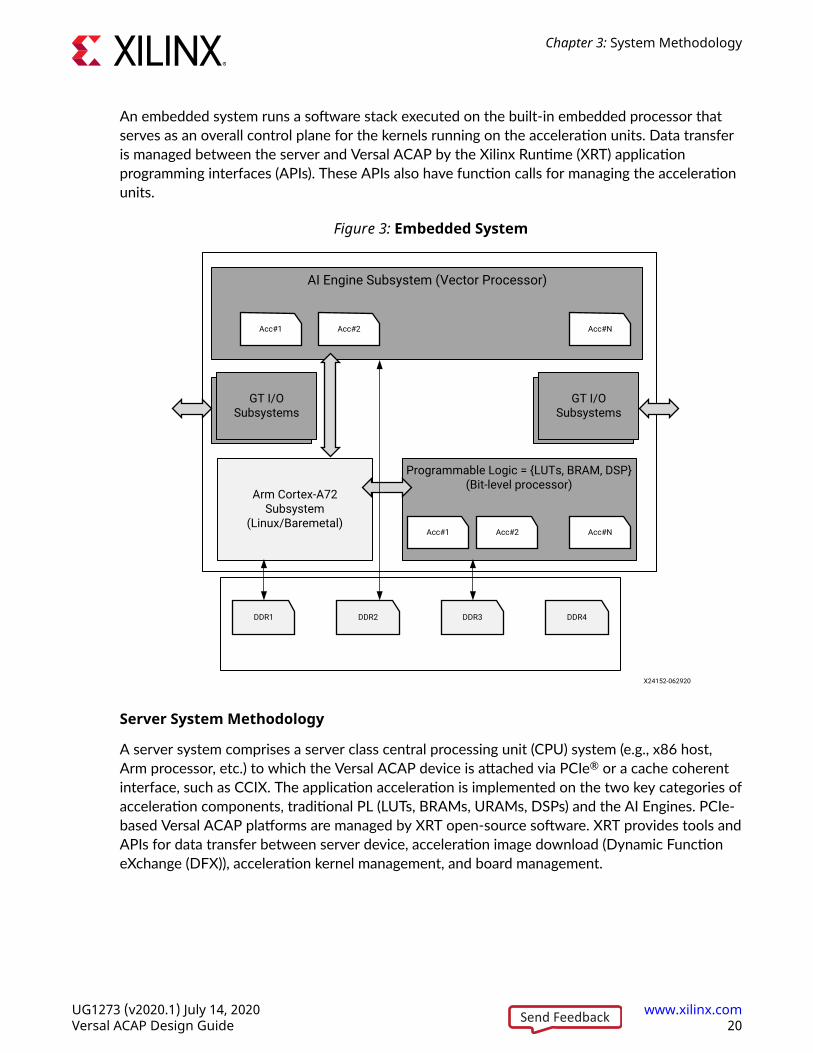
An embedded system runs a software stack executed on the built-in embedded processor thatserves as an overall control plane for the kernels running on the acceleration units. Data transferis managed between the server and Versal ACAP by the Xilinx Runtime (XRT) applicationprogramming interfaces (APIs). These APIs also have function calls for managing the accelerationunits.
Figure 3: Embedded System
Programmable Logic = {LUTs, BRAM, DSP}(Bit-level processor)
AI Engine Subsystem (Vector Processor)
Acc#1 Acc#2 Acc#N
PCIEGen4x16
OR CCIXv1.1
GT I/O Subsystems
PCIEGen4x16
OR CCIXv1.1
GT I/OSubsystems
Arm Cortex-A72 Subsystem
(Linux/Baremetal)Acc#1 Acc#2 Acc#N
DDR1 DDR2 DDR3 DDR4
X24152-062920
Server System Methodology
A server system comprises a server class central processing unit (CPU) system (e.g., x86 host,Arm processor, etc.) to which the Versal ACAP device is attached via PCIe® or a cache coherentinterface, such as CCIX. The application acceleration is implemented on the two key categories ofacceleration components, traditional PL (LUTs, BRAMs, URAMs, DSPs) and the AI Engines. PCIe-based Versal ACAP platforms are managed by XRT open-source software. XRT provides tools andAPIs for data transfer between server device, acceleration image download (Dynamic FunctioneXchange (DFX)), acceleration kernel management, and board management.
Chapter 3: System Methodology
UG1273 (v2020.1) July 14, 2020 www.xilinx.comVersal ACAP Design Guide 20Send Feedback
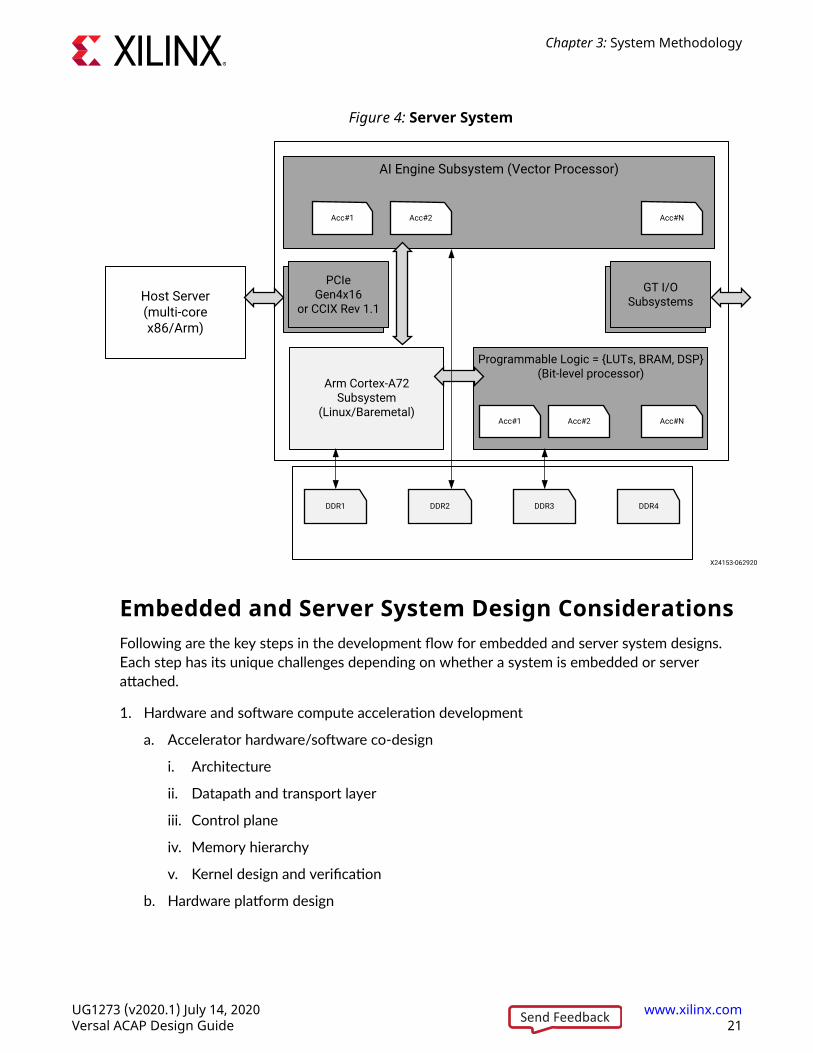
Figure 4: Server System
Programmable Logic = {LUTs, BRAM, DSP}(Bit-level processor)
Host Server(multi-core x86/Arm)
AI Engine Subsystem (Vector Processor)
Acc#1 Acc#2 Acc#N
PCIEGen4x16
OR CCIXv1.1
PCIeGen4x16
or CCIX Rev 1.1
PCIEGen4x16
OR CCIXv1.1
GT I/OSubsystems
Arm Cortex-A72 Subsystem
(Linux/Baremetal)Acc#1 Acc#2 Acc#N
DDR1 DDR2 DDR3 DDR4
X24153-062920
Embedded and Server System Design ConsiderationsFollowing are the key steps in the development flow for embedded and server system designs.Each step has its unique challenges depending on whether a system is embedded or serverattached.
1. Hardware and software compute acceleration development
a. Accelerator hardware/software co-design
i. Architecture
ii. Datapath and transport layer
iii. Control plane
iv. Memory hierarchy
v. Kernel design and verification
b. Hardware platform design
Chapter 3: System Methodology
UG1273 (v2020.1) July 14, 2020 www.xilinx.comVersal ACAP Design Guide 21Send Feedback
c. Design verification
i. Hardware and software co-simulation
ii. Performance validation
d. Timing closure
e. Hardware validation
i. Hardware and software bring-up and validation
ii. System debug
iii. Power and performance validation
2. Software development for effective use of hardware acceleration
a. Boot and OS considerations
b. Software application development
c. Software debug
Hardware and Software Compute Acceleration Development
Accelerator Hardware and Software Co-Design
The following accelerator design steps are common to both embedded and server systems:
1. Architecture
2. Datapath and transport layer
3. Control plane
4. Memory hierarchy
5. Kernel design and verification
Architecture
The primary challenge to resolve as part of system design architecture is power and performanceoptimization. Your choice of acceleration hardware, whether PL or AI Engines, depends on thetype of algorithm and data ingress and egress paths. In the case of streaming data ingress andegress to and from sensors (e.g., LiDAR, RADAR, dual-camera vision systems), data is available tofabric through high-speed transceivers. This data is aggregated from external protocol interfaceson AXI4-Stream buses and can be distributed to the PL or AI Engines.
The Scalar Engines (processor subsystem), Adaptable Engines (programmable logic), andIntelligent Engines (AI Engines) form a tightly-integrated, heterogeneous compute platform.Scalar Engines provide complex software support. Adaptable Engines provide flexible customcompute and data movement. Given their high compute density, AI Engines are well suited forvector-based algorithms.
Chapter 3: System Methodology
UG1273 (v2020.1) July 14, 2020 www.xilinx.comVersal ACAP Design Guide 22Send Feedback
During this step, you develop a mapping of the core application and of each algorithm to themost appropriate architectural area (e.g., AI Engine, PS, PL, NoC, DDRMC) in the Versal ACAP.This consists of mapping all of the major blocks in the application and considering requirementson these major blocks in terms of bandwidth and availability. This application mapping and designpartition step is manual.
You must consider which architecture is best for which task as follows:
• Scalar processing elements like CPUs are very efficient at complex algorithms with diversedecision trees and a broad set of libraries. However, these elements are limited in performancescaling. Application control code is well suited to run on the scalar processing elements.
• Programmable logic can be precisely customized to a particular compute function, whichmakes them best at latency-critical real-time applications (e.g., automotive driver assist) andirregular data structures (e.g., genomic sequencing). However, algorithmic changes havetraditionally taken hours to compile versus minutes.
• The AI Engine processors deliver more compute capacity per silicon area versus PLimplementation of compute-intensive applications. AI Engines also reduce compute-intensivepower consumption by 50% versus the same functions implemented in PL and also providedeterministic, high-performance, real-time DSP capabilities. Because the AI Engine kernels canbe written in C/C++, this approach also delivers greater designer productivity. Signalprocessing and compute-intensive algorithms are well suited to run on the AI Engines.
You can implement additional features, such as clock gating, for regions of the PL and AI Enginethat are not used concurrently. You can handle traditional multi-clock domain fabric design anddatapath clock domain crossing using the same approach that is used with FPGA architectures.
Datapath and Transport Layer
In an embedded design, the primary purpose of the datapath is to capture the dataflow ofinterest in the system application. For vision processing systems, the dataflow might includeincoming data from image sensors (e.g., camera, LiDAR, etc.) that is stored in on-chip and off-chipsystem memory (e.g., BRAM, URAM, DRAM) to be processed inline. For networking systems, thedataflow might be a protocol bridge between two standards like Ethernet and Interlaken.
In a server system, the datapath defines the primary dataflow between the server processorsystem and the Versal ACAP. There are two key datapath configurations that are available for theserver to attach to the Versal ACAP, PCI Express® or cache coherent interface. The PCI Expressdatapath allows standard PCI Express I/O transactions between the server and Versal ACAP. Thedatapath also supports more complex DMA transactions for the transfer of larger blocks ofinformation. The Versal ACAP CPM also includes support for cache coherent interconnect usinga protocol overlaid on the PCIe transport layer and enables a cache coherent view of the serversystem memory for all of the accelerators running on Versal ACAP.
The PL accelerators datapath (ingress and egress) is mapped to AXI4-Stream interfaces andcontrol interfaces, which are mapped to memory-mapped AXI interconnect. The control interfaceenables these accelerators to be controlled by the software stack.
Chapter 3: System Methodology
UG1273 (v2020.1) July 14, 2020 www.xilinx.comVersal ACAP Design Guide 23Send Feedback
Similarly, the AI Engine accelerators datapath is mapped to the AXI4-Stream interfaces. The AIEngine kernels have a run-time parameter (RTP) interface that enables run-time updates. You canaccess the RTP feature through the Xilinx run-time (XRT) APIs.
Control Plane
The control path orchestrates the system control functions, such as accelerator initialization, datatransfer initialization, and acceleration execution. Xilinx recommended using the XRT APIs forcontrol path design for both embedded and server systems. For more information, see the XRTRelease Notes (UG1451).
Memory Hierarchy
For data-intensive applications that demand high-bandwidth memory, the best approach is toconstruct a domain-specific memory hierarchy, such as memory caching from DDR to PL RAMs(URAM/BRAM). Versal devices can access the DDR memory through the NOCs. The DDR isconnected to the device fabric, and the Arm Cortex-A72 and the AI Engines are connectedthrough the NoC. Using DMA data movers in the PL, you can coordinate data movement to andfrom the hard IP to the DDR, leveraging the intermediate PL RAM stages for caching or databuffering.
Versal devices provide access to DDR memories using DMAs. The DDR memories are connectedto the device fabric and other hard IP through the hard memory controller and NoC. You can useDMA data movers in the PL to coordinate data movement to and from the DDR. You can alsoconfigure the NoC for maximum bandwidth using the DDR controllers available on the Versaldevice.
Following are additional recommendations:
• Use the NoC compiler to find the optimal solution for a required aggregate bandwidth.
• For data-intensive applications that demand high-bandwidth memory, construct a domain-specific memory hierarchy, such as memory caching from DDR to PL RAMs (URAM/BRAM).
Kernel Design and Verification
The accelerator kernels are the executable functional block implemented on the Versal ACAPplatform. There are two key types of kernels, AI Engine kernels and PL kernels:
• AI Engine kernels can be designed and simulated in the Vitis™ environment.
• PL kernels designed with register transfer level (RTL) languages can be individually simulatedin the Vivado® tools using AXI Verification IP (VIP).
• PL kernels designed in C/C++/OpenCL™ can be simulated using the Vitis HLS tool.
Chapter 3: System Methodology
UG1273 (v2020.1) July 14, 2020 www.xilinx.comVersal ACAP Design Guide 24Send Feedback
Hardware Platform Design
After the design architecture is complete, the next step is to create a Vitis platform thatcomprises several components, including CIPS, NoC, DDR, GTs, AI Engine, etc. Any number ofsubsequent designs can leverage a single platform. For more information, see the Vitis UnifiedSoftware Development Platform Documentation.
Design Verification
For information, see System Simulation Methodology.
Timing Closure
All typical timing closure practices that apply to the use of PL resources also apply to the PL inthe Versal ACAP. In addition, with the introduction of the hard AI Engine system that is physicallylocated above the fabric, the AI Engine compiler provides the directive for AI Engine-PL interfaceplacement.
Following are general guidelines to improve system-level timing closure issues:
• Leverage RTL and architecture design guidelines to achieve better design performance.
• Use AXI register slices to pipeline the AXI4-Stream datapath and assist the Vivado placer inspreading the logic in the fabric for better timing closure. The AXI register slice can also beused to help timing closure on the AI Engine-PL interface.
Software Development
Boot and OS
Versal devices have a centralized PMC that boots the device after power on reset. Versal devicessupport different boot modes, including JTAG, SD, eMMC, OSPI, QSPI, SelectMAP, and PCIeboot modes. Depending on the boot time requirement, you must select the appropriate bootdevice.
• For PCIe-based applications where there is a requirement to detect an Endpoint in less than100 ms of system power on, use a faster boot device like OSPI. The image can be partitionedso that a minimal boot image boots from the OSPI boot mode in less than 100 ms, and thelarger boot partition can be transferred over PCIe in Tandem PCIe boot mode.
• Use SD and eMMC boot devices for general embedded applications. Use eMMC boot modefor embedded applications that require higher density.
• Use JTAG boot mode for initial system bring-up and for debug. To enable system debug,switch to JTAG boot mode by configuring the boot mode register from the TAP chain.
Applications that require device-level security need to implement boot image encryption andauthentication supported by the Versal ACAP hardware. With encryption and authenticationenabled, there is a corresponding increase in the system boot time.
Chapter 3: System Methodology
UG1273 (v2020.1) July 14, 2020 www.xilinx.comVersal ACAP Design Guide 25Send Feedback
Versal ACAP boot devices support partition fallback to avoid catastrophic boot failure. During afield upgrade, if the upgraded image has an error, the PLM can fall back to a golden image torecover the boot mode. The golden image can reside in the same boot device as other upgradeimages.
Select the OS depending on your application-specific use case. For applications requiring buffermanagement, locked access, and interrupt handling with multiple processes running in parallel,use the Linux OS. These applications can leverage the open source Linux framework thatprovides higher level abstraction. Typical applications include video, OpenCL, OpenCV, andnetworking stacks that can leverage the Linux framework. Xilinx provides Linux run time supportusing the Xilinx run time (XRT) stack that handles interrupt management, starting and stopping ofkernels, buffer allocation, and sharing. XRT can interface with higher-level software stacks likeOpenCL, OpenCV, FFmpeg, and Python-based frameworks. One downside of using the Linux-based stack is the stack overhead, which is not suitable for real-time operations. Also, the LinuxOS requires FPD power to be on. Applications requiring significant power saving can use ArmCortex-R5F processor that works in LPD.
Applications that require real-time processing can leverage the Arm Cortex-R5F processors inVersal ACAP. Arm Cortex-R5F processors are ASIL-C safety compliant. Typical applicationmapping involves system monitoring, hardware monitoring, direct hardware control with lightweight stack, and so forth. If the Arm Cortex-R5F processor is targeted for a functional safetyapplication, Xilinx recommends fitting the application code in the TCM instead of accessing thecode from DDR memory. The Arm Cortex-R5F processor can also work as a co-processor to theLinux OS, monitoring specific hardware functionality and providing hardware status to the Linuxapplication. The communication between the Linux OS and RTOS/bare-metal OS on the ArmCortex-R5F can happen via the inter-processor interrupt.
Versal devices support virtualization. You can use the same hardware for multiple guest OS usinga hypervisor. There is a longer interrupt processing overhead with virtualized hardware.
For applications that require low latency processing, use dedicated hardware.
Software Application Development
To manage PL accelerators written in C/C++/OpenCL (HLS) or RTL, as well as AI Engine kernels,Xilinx recommends using the XRT APIs. Any IP that is in the platform must be explicitly managedby the designer. Any accelerator (PL or AI Engine) linked to the platform using the Vitis linker (v++ --link) is best managed by the XRT APIs. Tailor the design architecture to allow theapplication to reset the user-defined PL IP to a known good state to be able to handle errors. Youcan develop other high-level software applications using OpenCL, similar to previous 16 nmFPGA SDAccel™ flows. The Vitis tools provide a complete software development environment.
Software Debug
For information, see System Debug Methodology.
Chapter 3: System Methodology
UG1273 (v2020.1) July 14, 2020 www.xilinx.comVersal ACAP Design Guide 26Send Feedback
System Simulation MethodologyThe complexity of Versal ACAPs with its different compute domains challenges traditional FPGAsimulation methods. With traditional FPGA simulation, most of the design can be verified usinglogic simulation. With Versal ACAP, the programmable logic is only one of the compute domains,and the simulation methodology must consider the software domain as well as the AI Enginedomain when used.
The system simulation methodology for Versal ACAP is based on a hierarchical approach. Thismethodology acknowledges the need to simulate each compute domain independently, whilealso being able to simulate the entire system when appropriate.
The system simulation methodology is built around the following key concepts:
• Scope of the simulation: The simulation can include the entire system or just portions of thesystem. Xilinx recommends testing blocks and functions individually before integrating andsimulating them in the entire system. You can use different simulation flows to test thedifferent compute domains, including the PS, PL, and AI Engine.
• Abstraction of the simulation: In some cases, you can simulate specific functions at differentabstraction levels. This is true of both AI Engine and HLS code, which you can simulate eitheras untimed or as cycle-accurate models. This is also the case for specific Versal ACAPinfrastructure blocks, such as the NoC or DDR controllers, which you can simulate as SystemCtransaction-level models (TLM) or RTL models. Abstraction allows you to trade simulationspeed for simulation accuracy.
• Purpose of the simulation: The purpose of each simulation can vary. For example, is the focuson functional validation or performance measurement? Is the intention to test a singlefunction or the interactions between multiple functions? Different simulation purposes rely ondifferent simulation setups and configurations. Purpose is closely related to scope andabstraction.
Related InformationSimulation Flows
Simulation RecommendationsFollowing are Versal ACAP simulation recommendations:
• Choose the appropriate simulation flow and abstraction based on the scope and intendedpurpose.
• Simulate and verify each component individually before integrating them and runninghardware emulation, including the AI Engine graph, HLS kernels, RTL blocks, hardwareplatform, and PS code.
Chapter 3: System Methodology
UG1273 (v2020.1) July 14, 2020 www.xilinx.comVersal ACAP Design Guide 27Send Feedback
• Reuse test benches and test vectors whenever possible when testing different blocks andfunctions. For example, if the output of one block is the input to another block, reusing testvectors to simulate these two blocks eases the integration process.
• Perform gradual system integration. You do not need to run hardware emulation on the entiresystem. Running hardware emulation with a subset of the PS, PL, and AI Engine componentscan establish a known foundation, and you can gradually add functionality.
• Simulate and verify every design change. The earlier an issue is caught, the easier it is toaddress.
System Debug MethodologyThe Versal ACAP includes an HSDP feature that enables enhanced system debug methodologycapabilities. This feature is designed to work in any environment, including the lab, data center,and edge computing environments.
The HSDP feature consists of a centralized debug packet controller (DPC), which is the packetprocessing engine of the HSDP. The packets that are processed by the DPC are referred to as thedebug and trace packets (DTP). These packets are decoded by the DPC to determine thecommands, the destinations, and any potential higher-level flow control and management tasks.The DPC processes the DTP sent by a host, executes any commands embedded in the packets,and generates responses that are sent back to the host.
The HSDP DPC can be accessed from any of the following interfaces:
• JTAG interface
• Integrated Aurora via GTs
• PL fabric (using soft Aurora, PCIe, or any other suitable interface)
• PCIe interface
The HSDP feature enables debug of the use cases described in the following sections.
Note: The various APUs and RPUs of the PS can be debugged via the Arm CoreSight™ infrastructure that isintegrated into the PS. The CoreSight infrastructure is accessible via the JTAG-DAP and HSDP interfaces.
Chapter 3: System Methodology
UG1273 (v2020.1) July 14, 2020 www.xilinx.comVersal ACAP Design Guide 28Send Feedback
Debug via JTAGThe PMC includes a JTAG interface that can be used for both programming and debuggingdesigns running on the Versal ACAP. The JTAG interface consists of two cascaded blocks: thedebug access port (DAP) and test access port (TAP). The DAP is primarily used to access thevarious debug features of the PS and can also be used for low-bandwidth read/write access toany accessible register and memory location within the address range of the PS. The TAPinterface is primarily used for accessing the device configuration and boundary scaninfrastructure, and also includes instructions for configuring and accessing the HSDP DPCfunctionality.
Debug via AuroraThe PS includes an integrated Aurora 64B/66B block that is dedicated for use in accessing theHSDP function via a high-speed GT-based interface. The Aurora interface to the HSDP DPCprovides bidirectional access to the device from an external host debug/trace cable, allowing forhigh-speed debug and trace operations.
Note: The integrated Aurora interface is not available in all Versal ACAPs.
Debug via PL FabricThe HSDP DPC can also be accessed from the PL fabric. This allows you to integrate HSDP intoyour systems using methods other than the dedicated CPM/PCIe pathway, integrated Aurora,and JTAG.
Debug via PCIeIn data center applications and other PCIe interface-hosted systems, the HSDP DPC can beaccessed via the same PCIe interface in the CPM that is used for host-to-ACAP communication.You can choose how to map the HSDP function to a PCIe physical function and BAR space. TheHSDP function includes a dedicated HSDP DMA engine that is used to move debug databetween the HSDP and host memory.
Note: CPM availability is device specific. For information, see the Versal Architecture and Product Data Sheet:Overview (DS950).
Debugging the AI EngineEvery AI Engine in the AI Engine array has a debug interface, which can be used to read/write toall the individual AI Engine registers. The following files can be read and written over thisinterface: scalar register files, vector register files, status registers (for overflow, saturation, etc.),special registers like stack pointer, and zero overhead loop registers.
Chapter 3: System Methodology
UG1273 (v2020.1) July 14, 2020 www.xilinx.comVersal ACAP Design Guide 29Send Feedback
Requests for reading and writing AI Engine registers are sent via the AXI4 memory-mapped(AXI4-MM) interface and are then forwarded to the AI Engine Debug Interface. All the registersin the AI Engine are mapped on the AXI4-MM. The AXI4-MM interface has a 32-bit read/writebus. You can specify any AXI4-MM mapped address to read over the AXI4-MM interface. Anyexternal AXI4-MM master (e.g., PS) can issue a stall signal to a specific AI Engine by writing intothe control/status register. There are independent registers for system control (e.g., normalprogram flow) and the debugger. The Vitis System Debugger provides a comprehensive sourcecode debugger that helps debug AI Engine graphs and kernels.
Events are another important feature of AI Engine debug and performance analysis. Events aresimilar to triggers. An event signal is high in the cycle for which the condition associated withthat event is true. Examples of events include Conflict DM bank 0, Lock 11 Released, Floatingpoint Overflow, and PC event 0. Each event has a unique 7-bit number, and there are up to 128events in each AI Engine. Following are additional details:
• Event Actions: can be configured to perform a task whenever a specific event occurs.Examples of event actions include Debug halt core, Single step core, and IncrementPerformance Counter.
• Event Broadcast: can be used to send events signals to a neighboring AI Engine and the PL.
• Event Trace Unit: can collect cycle-by-cycle event activity from 8 numbered event signals andsend compressed trace information from the AI Engine array via the AXI4-Stream network.The Vitis environment allows you to capture specific events from an AI Engine that can beanalyzed in the Vitis Analyzer tool.
Debugging the PSThe DAP supports Arm CoreSight debug and trace of the PS. This includes both secure and non-secure debug support. The DAP also interfaces to external Arm debug tools via JTAG, accordingto Arm debug interface version 5 (ADIv5). TAP has access via JTAG Boundary Scan to theERROR_STATUS register containing various error and alarm status bits. The Vitis SystemDebugger provides an integrated design environment (IDE) for PS debug with Baremetal andLinux-based applications.
Chapter 3: System Methodology
UG1273 (v2020.1) July 14, 2020 www.xilinx.comVersal ACAP Design Guide 30Send Feedback
Chapter 4
Design FlowXilinx recommends using the Vitis™ and Vivado® tools to create and migrate designs targeted toVersal™ ACAPs. The design flows are similar to the flows used when targeting previousarchitectures.
The Versal ACAP Vitis environment supports a variety of applications that target the following:
• Server systems with the x86 host communicating through PCIe® blocks with a Xilinx®
acceleration platform and with Vitis kernels in the PL and in the AI Engines
• Embedded systems with the PS (Arm® processor-based) host communicating with a VivadoDesign Suite PL design packaged as a hardware platform and with Vitis kernels in the PL andin the AI Engines
• Embedded systems with the PS (Arm processor-based) host communicating with a VivadoDesign Suite PL design packaged as a hardware platform
The Versal ACAP Vivado tools support creation of hardware platforms and designs either usingthe Vivado IP integrator or register transfer level (RTL).
Note: Depending on your design flow, you run either the Vitis or Vivado tools. If you are running the Vitistools, the Vivado tools are run automatically at certain points during the flow.
Vitis Environment Design FlowVersal ACAP designs are enabled by the Vitis tools, libraries, and IP. The Vitis environment letsyou program, run, and debug the different elements of a Versal ACAP AI Engine application,which can include AI Engine kernels and graphs, PL, high-level synthesis (HLS) IP, RTL IP, and PSapplications. Each domain has its own set of tools and methodologies. For more information, seethe Vitis Unified Software Development Platform Documentation.
Chapter 4: Design Flow
UG1273 (v2020.1) July 14, 2020 www.xilinx.comVersal ACAP Design Guide 31Send Feedback
The Vitis environment includes AI Engine tools for programming, debugging, and deploying graphalgorithms, including the aiecompiler, SystemC simulator (aiesimulator), and x86 simulator(x86simulator). The Vitis compiler (v++ --compile) allows integration of kernels to the graphrunning in the PL region of the device or running alongside the graph to define additionalsubsystems. The Vitis embedded software development flow (with the system software stackincluding PetaLinux) provides support for the PS domain of the embedded processor. The Vitisenvironment facilitates the creation and integration of subsystems for each of these domains,providing standardized interface requirements and data handoff between the different domains.
The Vitis tools take a platform-based approach, separating the essential services provided by theplatform from the user-specific features of the application provided through the subsystems.
Platforms
Platforms come in two halves, the hardware platform and the software platform. The hardwareplatform includes the PS, NoC, DDR controllers, primary I/Os, AI Engine array, and any otheruser-specified IP blocks. The software platform defines the domains, device tree, and OS.
The platform insulates application developers from the details of low-level infrastructure and letsthem focus on development of a specific subsystem function, such as software, AI Engine graph,or PL kernel logic. It is common for application developers to start their work by targeting astandard Xilinx platform before transitioning to a custom platform developed for a specific boardand application. Custom platforms are developed using the Vivado tools.
Subsystems
Subsystems perform well-defined functions within the application. Subsystems are designed,debugged, and eventually integrated with other subsystems to form the top-level application.Using this approach, a complete Versal ACAP system is built using a collection of subsystems ona platform. This approach is similar to designing large FPGA designs.
A subsystem can include PS firmware, AI Engine graphs, and PL kernels. The subsystem is astandalone functional entity, performing well-defined functions under the supervision andcoordination of the PS or PL. The subsystem always includes controlling software that configuresthe system as well as orchestrates the execution of subsystems in the AI Engine and PL fabric. Asubsystem can interact with other subsystems via shared memory and streams.
The PL and AI Engine components of a subsystem are assembled using the Vitis compiler andlinker (v++ --compile and v++ --link), and the PS firmware is integrated with the Vitispackager (v++ --package).
Note: Currently, the AI Engine domain can only be part of a single subsystem.
Chapter 4: Design Flow
UG1273 (v2020.1) July 14, 2020 www.xilinx.comVersal ACAP Design Guide 32Send Feedback
Developing independent subsystems allows the concurrent development of multiple subsystemsand integration into the platform. Custom platform development can also occur at the same timeas application development, allowing simultaneous development of the custom application andthe custom platform to deploy the application. The top-level system project comprises multiplesubsystems, whether delivered by one team working on different elements at different times orby multiple teams working on multiple subsystems to build the system.
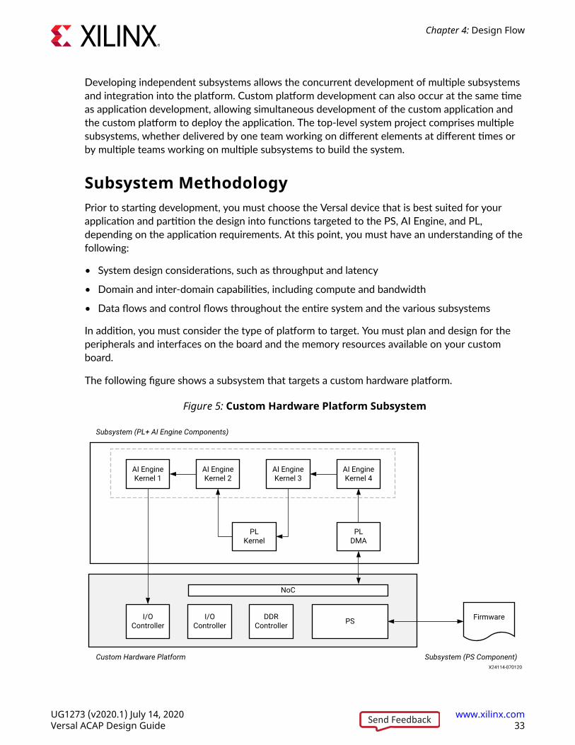
Subsystem MethodologyPrior to starting development, you must choose the Versal device that is best suited for yourapplication and partition the design into functions targeted to the PS, AI Engine, and PL,depending on the application requirements. At this point, you must have an understanding of thefollowing:
• System design considerations, such as throughput and latency
• Domain and inter-domain capabilities, including compute and bandwidth
• Data flows and control flows throughout the entire system and the various subsystems
In addition, you must consider the type of platform to target. You must plan and design for theperipherals and interfaces on the board and the memory resources available on your customboard.
The following figure shows a subsystem that targets a custom hardware platform.
Figure 5: Custom Hardware Platform Subsystem
Subsystem (PL+ AI Engine Components)
AI Engine Kernel 1
AI Engine Kernel 2
AI Engine Kernel 3
AI Engine Kernel 4
PLKernel
PLDMA
I/O Controller
I/O Controller
DDR Controller PS
NoC
Firmware
Custom Hardware Platform Subsystem (PS Component)X24114-070120
Chapter 4: Design Flow
UG1273 (v2020.1) July 14, 2020 www.xilinx.comVersal ACAP Design Guide 33Send Feedback
The Vitis design flow is an iterative process that might loop through each step multiple times,adding layers or elements to the subsystem through subsequent iterations. Teams can iteratethrough the early steps more quickly and take more time with later steps, which provide moredetailed performance data.
Following are the recommended steps for creating your design in the Vitis environment.
• Kernel and Graph Development: This step includes the development and functionalverification of application kernels. These kernels can run on the AI Engine domain or the PLdomain.
• Subsystem Assembly and Verification Using Hardware Emulation: This step includesassembling the AI Engine and PL kernels with the platform as well as building for hardwareemulation using a Xilinx standard platform.
• Subsystem Assembly and Verification on Hardware: This step includes building the subsystemagainst the Xilinx standard platform and testing in real hardware on a Xilinx standard board.
• Subsystem Integration on Custom Platform: This step includes building the subsystem againstyour custom platform and testing using your custom board.
The Vitis environment design flow makes a distinction between platforms and subsystems, whichinsulates subsystem developers from internal platform details and allows them to build fullyfunctional designs independently. The first three steps of the subsystem design flow assume youare using Xilinx-provided platforms and you are integrating the subsystem to your customplatform in the final step. The custom platform is developed using the Vivado Design Suite andcan happen in parallel with the subsystem, which is developed using the Vitis tool flow. Thisapproach reduces risk and uncertainty and increases the chances of success when integrating thesubsystem with the custom platform.
Kernel and Graph DevelopmentThe first step in this design flow includes the development and functional verification of theindividual components of the subsystem: AI Engine graph and PL kernels (HLS and/or RTL).During this step, these components are typically developed and tested independently from oneanother. However, it is possible to use the Vitis environment hardware emulation flow to starttesting the integration of these components.
In this step, verification focuses primarily on functional considerations. Performance informationgenerated for each component typically assumes ideal I/O patterns and no backpressure withdata always available. However, it is important to make note of the available performance data,because the system performance is not likely to improve as you progress through your design. Besure to meet your performance objectives in each step, starting with the first step in the designflow.
Chapter 4: Design Flow
UG1273 (v2020.1) July 14, 2020 www.xilinx.comVersal ACAP Design Guide 34Send Feedback
Developing the AI Engine Graph and Kernels
An AI Engine program comprises a data-flow graph specification written in C++, which consistsof nodes and edges. Nodes represent compute kernel functions, and edges represent dataconnections. Kernels in the application can be compiled to run on the AI Engines or in the PLregion of the device. The AI Engine graph specification is compiled using the aiecompiler andexecuted with the aiesimulator.
Xilinx recommends gradually refining and testing the graph, slowly progressing from scalar tovectorized operations. Using scalars, you can target AI Engine tiles without having to code withintrinsics right away. This allows you to set up your system (e.g., build scripts, functionalcorrectness, etc.) without having to do low-level AI Engine coding.
The graph is tested with a user-written test bench that drives and manages the graph using thegraph APIs. The test bench and graph APIs serve as the foundation for the development of PSfirmware in later steps. There are multiple methods for getting data into and out of a graph. Run-time parameters (RTPs) are programmable registers for scalar values. GMIOs provide a directconnection from the AI Engine to global memory. Streaming connections provide a directconnection between AI Engine kernels and PL kernels modeled with PLIOs in the simulation. Atthis stage in development, file I/O is often the simplest and most effective way to get data intoand out of your graph.
Meeting performance in the aiesimulator at this early stage in the design is not a benchmark ofthe final system performance, because performance data is idealistic at this point. The impact ofgoing out of or into the graph through the PLIOs is difficult to model, which limits the ability toaccurately estimate performance.
Developing PL Kernels with Vitis HLS
PL kernels can be developed using C/C++ code and the Vitis HLS tool. The Vitis HLS toolsimplifies the use of C/C++ functions for implementation as PL kernels in the Vitis applicationacceleration development flow.
The Vitis HLS tool automates much of the code modifications required to implement andoptimize the C/C++ code in programmable logic and to achieve low latency and high throughput.The Vitis HLS tool allows inference of required pragmas to produce the right interface for yourfunction arguments and to pipeline loops and functions within your code.
Note: Although HLS development is done outside of the AI Engine tool environment, it is possible tooptionally include HLS kernels in the AI Engine graph C++ specification.
The Vitis HLS design flow includes the following main steps:
1. Compile, simulate, and debug the C/C++ algorithm.
2. View reports to analyze and optimize the design.
3. Synthesize the C algorithm into an RTL design.
Chapter 4: Design Flow
UG1273 (v2020.1) July 14, 2020 www.xilinx.comVersal ACAP Design Guide 35Send Feedback
4. Verify the RTL implementation using RTL co-simulation.
5. Compile the RTL implementation into a compiled object file (.xo), or export to an RTL IP.
For more information, see the Vitis High-Level Synthesis User Guide (UG1399).
Developing PL Kernels with RTL and the Vivado Design Suite
PL kernels can also be developed using RTL kernels and the Vivado Design Suite. This approach isconvenient for hardware engineers that have existing RTL IP, including Vivado IP integrator-based designs, or prefer creating new functions by writing RTL code.
An RTL kernel is a regular design packaged as Vivado Design Suite IP, but the kernel must complywith specific interface rules and requirements to be usable in the Vitis environment design flow.For more information about RTL kernels, see RTL Kernels in the Application AccelerationDevelopment flow of the Vitis Unified Software Platform Documentation (UG1416).
Creating an RTL kernel follows traditional RTL design guidelines. Xilinx highly recommends thatyou create custom test benches and use behavioral simulation to thoroughly verify the RTL codebefore packaging and using the code as PL kernels in the Vitis environment design flow. After anRTL design is fully verified and meets all the requirements for a Vitis kernel, the design can becompiled into a Vitis kernel object (XO file) using the package_xo command.
Subsystem Assembly and Verification UsingHardware EmulationIn the second step of this design flow, you gradually assemble subsystem components (PS, PL,and AI Engine) on top of the target platform and use the Vitis hardware emulation flow tosimulate the integrated system. Hardware emulation is a cycle approximate simulation of thesystem. The AI Engine graph runs in the SystemC simulator. RTL behavioral models of the PL runin the Vivado simulator or a supported third-party simulator. The software code executing on thePS is simulated using the Xilinx Quick Emulator (QEMU).
The target platform contains all of the necessary hardware and software infrastructure resourcesrequired for the project. It is possible to target a standard Xilinx platform or a custom platform foryour project. At this step in the flow, Xilinx recommends using a standard and pre-verifiedplatform to reduce uncertainty in the process and focus efforts on the system components (graphand kernels).
The Vitis linker (v++ --link) is used to assemble the compiled AI Engine graph (libsdf.a)and PL kernels (.xo) with the targeted platform. The Vitis linker establishes connections betweenthe AI Engine ports, PL kernels, and other platform resources.
Chapter 4: Design Flow
UG1273 (v2020.1) July 14, 2020 www.xilinx.comVersal ACAP Design Guide 36Send Feedback
Because this design flow progresses gradually, certain elements might not exist in early iterations.You might need to terminate unconnected signals, drive signals, or provide sinks. In this case,unterminated streaming connections between the AI Engine graph and PL kernels (PLIOs andAXI4-Stream) require the addition of simulation I/Os and traffic generator IP for emulationpurposes, which can be added during the linking process using v++ options.
The Vitis linker automatically inserts FIFOs on streaming interfaces as well as clock domainconverters (CDC) and data width converters (DWC) between the AI Engine and PL kernels asneeded. On the Versal ACAP, the clock on the AI Engine array can run at 1 GHz, but the clock inthe PL region runs at a different, lower frequency. This means there can be a difference betweenthe data throughput of the AI Engine kernels and the PL kernels based on their clock frequencies.When linking the subsystem, the Vitis compiler can insert CDCs, DCWs, and FIFOs to match thethroughput capacities of the PL and AI Engine regions.
The Vitis packager (v++ --package) is used to add the PS application and firmware and togenerate the required setup to run hardware emulation. The PS application controls the AIEngine graph, including how it is loaded, initialized, run, and updated, and the PL kernels. Tocontrol the AI Engine graph, you must use the graph APIs generated by the aiecompiler or thestandard XRT APIs. To control the PL kernels, Xilinx recommends using the standard XRT APIs.XRT is an open-source library that makes it easy to interact with PL kernels and AI Engine graphsfrom a software application, either embedded or x86-based.
Optionally, you can build higher-level functionality on top of the graph and PL drivers. For the PSsubsystem, you write code in this step that did not fully exist in the first step. Drivers or firmwareinteract directly with the kernels and a higher-level application that uses these drivers.
You can develop PS firmware, graph drivers, and PL kernels as follows:
• PS firmware: Use the test bench from the first step in the design flow, which drives andmanages the graph using graph APIs.
• Graph drivers: Use the graph APIs to test the graph and to interact with RTPs and GMIOs.
• PL kernel drivers: Use XRT APIs or UIO drivers to interact with the PL kernels.
In this step, most models are cycle accurate. However, some models are only approximate, andother models are transaction-level models (TLM). PL kernels are simulated using the target clock,which is not guaranteed to be met during implementation. The interactions between the AIEngine graph and PL kernels are modeled at the cycle level, but overall accuracy depends on theaccuracy of the patterns produced by the traffic generators and other test bench modules. Theimpact of other subsystems or complex I/O interactions cannot be accurately modeled. Theslower performance of the emulation environment limits the number of traffic/vectors that canbe tested.
Note: Meeting performance in hardware emulation is necessary but is not a guarantee of results. Hardwareemulation is cycle approximate with better accuracy in performance than during the first step in the designflow. However, performance results are still not final at this stage.
Chapter 4: Design Flow
UG1273 (v2020.1) July 14, 2020 www.xilinx.comVersal ACAP Design Guide 37Send Feedback
Subsystem Assembly and Verification on HardwareAfter hardware emulation provides a good view of the subsystem, you can proceed to thehardware build on a Xilinx standard platform. Targeting a Xilinx standard platform helps toeliminate some uncertainty from the test environment.
In this step, you are reusing the subsystem from the previous step but are now targeting thehardware build. Using the Vitis linker, you take the assembled PL kernels through synthesis andplace and route. Using the Vitis packager, you package the PS and AI Engine programs togenerate the required output files to load and run the application on the Xilinx standarddevelopment board.
In the early stages of the design, this step is similar to iterating through Vivado synthesis, placeand route, and timing closure to achieve optimal results. Iterate until the performance objectivesare met, including Fmax, throughput, and resource utilization.
Like the previous two steps of this design flow, this step also allows an incremental approach inwhich different components are gradually added to the subsystem and taken to hardware. Thisgradual approach allows you to safely build upon previously verified components, which is aproven strategy to manage design complexity.
From a performance standpoint, running in real hardware gives you more accurate numbers thanrunning in hardware emulation. Potential sources of differences between this step and thepreceding step include the following:
• Implementation results in potentially lower clock frequency
• More accurate execution profile of control code running on the PS
• More realistic I/O patterns, resulting in more realistic exercising of stalls and back pressure
• Discovery of corner cases that cannot be reached in the slower hardware emulation runs
Subsystem Integration on Custom PlatformIn the final step of this flow, all the elements of the subsystem from the preceding step areintegrated and built on the custom platform, which was developed to deploy the application. Thisstep is similar to the previous step but uses the custom platform instead of a Xilinx platform.
The goal of this step is to meet timing and performance closure on the actual target platform. Byrunning through Vivado synthesis and place and route, you can address any differences in timing,utilization, and power that occur when you switch from the Xilinx standard platform to yourcustom platform.
Chapter 4: Design Flow
UG1273 (v2020.1) July 14, 2020 www.xilinx.comVersal ACAP Design Guide 38Send Feedback
This step also allows you to test and debug the custom platform as well as the application andsubsystem. Testing the subsystem with external I/Os means you might encounter somedifferences between the previous step and this step in the hardware execution. However, if youdesigned your custom platform correctly, the standardized interfaces of the platform can insulatesubsystem testing from such differences.
Vivado Tools Design FlowThe Vivado Design Suite offers multiple ways to accomplish the tasks involved in Xilinx devicedesign, implementation, and verification. You can use the traditional register transfer level (RTL)to device configuration design flow. You can also use system-level integration flows that focus onintellectual property (IP)-centric design and C-based design. Design analysis and verification isenabled at each stage of the flow. Design analysis features include logic simulation, I/O and clockplanning, power analysis, constraint definition and timing analysis, design rule checks (DRC),visualization of design logic, analysis and modification of implementation results, programming,and debugging.
IMPORTANT! Most Versal ACAP designs are created with the Vitis environment design flow and require a Vitishardware platform. Xilinx provides standard platforms as starting points, which can be customized andregenerated by the Vivado IP integrator to better fit the target system application.
System Hardware Design FlowXilinx highly recommends using the Vivado IP integrator cockpit for designs that target VersalACAPs. The Vivado IP integrator lets you create complex system designs by instantiating andinterconnecting IP cores from the Vivado IP catalog onto a design canvas. The Vivado IPintegrator is designed to simplify Versal ACAP AXI-based IP connectivity.
Vivado IP Integrator
The following sections provide information on significant IP that you can access from the VivadoIP integrator to create and configure your Versal ACAP design. For usage information and generalhardware platform generation information, see the Vivado Design Suite User Guide: Designing IPSubsystems Using IP Integrator (UG994).
Versal CIPS IP Core
The CIPS IP allows you to configure the following:
• Device clocking to the PMC, PS, NoC, and optionally, PL
• PS peripherals and their associated I/O
• PS-PL interrupts and cross-triggering
Chapter 4: Design Flow
UG1273 (v2020.1) July 14, 2020 www.xilinx.comVersal ACAP Design Guide 39Send Feedback
• CPM (the integrated block for PCIe with DMA and cache coherent interconnect)
• PS and CPM AXI interfaces to NoC and PL
• System Monitor supply and temperature monitoring and alarms
• HSDP for high-speed debugging
Versal AI Engine IP
The AI Engine is configured using the AI Engine IP, which lets you define the number of:
• AXI4-Stream master and slave interfaces to and from the AI Engine and PL
• AXI4-Stream clock ports for the PL and NoC channels
• Memory-mapped AXI interfaces to and from the AI Engine to the NoC
• Events being triggered and monitored both from AI Engine and the PL
Note: AI Engine IP is used only for custom platform creation.
Versal AXI NoC IP
The NoC is configured using the AXI NoC IP. The IP acts as logical representations of the NoC.The AXI NoC IP supports the AXI memory-mapped protocol, and the AXIS NoC IP supports theAXI4-Stream protocol. A Versal ACAP design can include multiple instances of each type of IP.
The DDRMC is integrated into the AXI NoC IP. An instance of the AXI NoC can be configured toinclude one, two, or four instances of the DDRMC. You must use the NoC IP to communicatewith the integrated DDRMC. During the validate step, the Versal NoC compiler is run on theunified traffic specification. After validation, the NoC Viewer window allows you to review andedit the NoC solution.
For configuration details on the NoC and related IP as well as details on the system address map,see the Versal ACAP Programmable Network on Chip and Integrated Memory Controller LogiCORE IPProduct Guide (PG313).
Versal Clocking Wizard
The Versal Clocking wizard generates source RTL code to implement a clocking network matchedto your requirements. This wizard generates the clocking network for all Versal clockingprimitives.
Versal Transceivers Bridge
The Versal ACAP transceivers are highly configurable and tightly integrated with the PL block.The Versal Transceiver Bridge enables Vivado IP integrator-based design entry for GT-based IP.This allows you to generate designs that use multiple quads or designs that share quads withmultiple protocol IP. You must use the Advanced I/O planner to add physical GT locations.
Chapter 4: Design Flow
UG1273 (v2020.1) July 14, 2020 www.xilinx.comVersal ACAP Design Guide 40Send Feedback
Versal Advanced I/O Wizard
The I/O planning flow for high-performance I/O in Versal ACAP includes significantimprovements from previous devices. The I/O planning flow is unified for both memory and non-memory interfaces in the Advanced I/O Planner. If you previously generated high-performanceinterfaces using the High-Speed SelectIO™ wizard or SelectIO component mode, you mustrebuild the interfaces using the Versal Advanced I/O wizard, which now supports multi-bankinterface generation.
Design Address Map
The Versal ACAP uses a single, unified system address map. All memory-mapped AXItransactions must adhere to this map. The Versal ACAP system address map defines the defaultaddress locations of slaves in the Versal ACAP. The address map is built into the fabricinterconnect and the NoC. The Vivado IP integrator automatically resolves the base name, offsetaddress, and range of the address region based on the DDR4 memory options selected in the AXINoC IP customization. These addresses are used by the AXI master to communicate with theDDR. You use the Vivado IP integrator Address Editor to select or automatically assign compliantaddresses for all the memory-mapped blocks within the design. For configuration details on theNoC and related IP as well as details on the system address map, see the Versal ACAPProgrammable Network on Chip and Integrated Memory Controller LogiCORE IP Product Guide (PG313).
RTL Design FlowThe RTL design flow is provided for designers that do not want to use Vivado IP integrator. If youchoose not to use Vivado IP integrator, essential automation related to the CIPS and NoC IP isnot available, including the following:
• PS functions (e.g., Arm cores)
• Automation across all blocks connected to CIPS and NoC
• Connection automation between CIPS and NoC
In a pure RTL flow, you can instantiate the CIPS IP primarily for accessing device configurationfeatures and use the NoC to exclusively connect several AXI masters in the PL to one or severalDDRMC IP. Alternatively, you can use Vivado IP integrator to integrate and configure the CIPS IPand NoC IP together, specify the interface to the rest of the design, and instantiate the resultingblock design in the top-level RTL. Although the final method allows access to all Versal ACAPadvanced hardware features, the design must maintain both the RTL and the block design inparallel when making any functionality or connectivity change.
Chapter 4: Design Flow
UG1273 (v2020.1) July 14, 2020 www.xilinx.comVersal ACAP Design Guide 41Send Feedback
Vivado IP Catalog
The following sections provide information on essential IP that you can access from the VivadoIP catalog to create and configure your Versal ACAP design.
Versal CIPS IP
The CIPS IP allows you to configure the following:
• Device clocking to the PMC, PS, NoC, and optionally, PL
• PS peripherals and their associated I/O
• PS-PL interrupts and cross-triggering
• CPM (the integrated block for PCIe with DMA and cache coherent interconnect)
• PS and CPM AXI interfaces to NoC and PL
• System Monitor supply and temperature monitoring and alarms
• HSDP for high-speed debugging
Versal AXI NoC IP
Depending on your design, you can use the IP in one of the following ways:
• In designs with fabric-based logic that access the DDRMC, you can use the AXI NoC IP fromthe Vivado IP catalog.
• In designs where the DDR memory is shared across the PL and the PS, you must use theVivado IP integrator design flow to create a block design (BD) with at least both CIPS and AXINoC IP and instantiate the BD in the RTL design.
The NoC is configured using the AXI NoC IP. The IP acts as logical representations of the NoC.The AXI NoC IP supports the AXI memory-mapped protocol, and the AXIS NoC IP supports theAXI4-Stream protocol. A Versal ACAP design can include multiple instances of each type of IP.
The DDRMC is integrated into the AXI NoC IP. An instance of the AXI NoC can be configured toinclude one, two, or four instances of the DDRMC. You must use the NoC IP to communicatewith the integrated DDRMC. During the validate step, the Versal NoC compiler is run on theunified traffic specification. After validation, the NoC Viewer window allows you to review andedit the NoC solution.
For configuration details on the NoC and related IP as well as details on the system address map,see the Versal ACAP Programmable Network on Chip and Integrated Memory Controller LogiCORE IPProduct Guide (PG313).
Chapter 4: Design Flow
UG1273 (v2020.1) July 14, 2020 www.xilinx.comVersal ACAP Design Guide 42Send Feedback
Versal Clocking Wizard
The Versal Clocking wizard generates source RTL code to implement a clocking network matchedto your requirements. This wizard generates the clocking network for all Versal clockingprimitives.
Versal Transceivers Wizard
The Versal ACAP transceivers are highly configurable and tightly integrated with the PL block.The Versal Transceivers wizard automatically generates XDC file templates that configure thetransceivers and contain placeholders for transceiver placement information. This wizard alsosupports generating example designs to simulate key features like rate switching and quadsharing across various protocols.
Note: The Vivado IP integrator is recommended for designs sharing GT quads.
Versal Advanced I/O Wizard
The I/O planning flow for high-performance I/O in Versal ACAP includes significantimprovements from previous devices. The I/O planning flow is unified for both memory and non-memory interfaces in the Advanced I/O Planner. If you previously generated high-performanceinterfaces using the High-Speed SelectIO™ wizard or SelectIO component mode, you mustrebuild the interfaces using the Versal Advanced I/O wizard, which now supports multi-bankinterface generation.
Design Address Map
The Versal ACAP uses a single, unified system address map. All memory-mapped AXItransactions must adhere to this map. The Versal ACAP system address map defines the defaultaddress locations of slaves in the Versal ACAP. The address map is built into the fabricinterconnect and the NoC. The Vivado IP integrator automatically resolves the base name, offsetaddress, and range of the address region based on the DDR4 memory options selected in the AXINoC IP customization. These addresses are used by the AXI master to communicate with theDDR. You use the Vivado IP integrator Address Editor to select or automatically assign compliantaddresses for all the memory-mapped blocks within the design. For configuration details on theNoC and related IP as well as details on the system address map, see the Versal ACAPProgrammable Network on Chip and Integrated Memory Controller LogiCORE IP Product Guide (PG313).
ImplementationYou must use Vivado tools for synthesis and implementation. The Versal ACAP includes newprimitives that the Vivado synthesis tool infers.
Chapter 4: Design Flow
UG1273 (v2020.1) July 14, 2020 www.xilinx.comVersal ACAP Design Guide 43Send Feedback
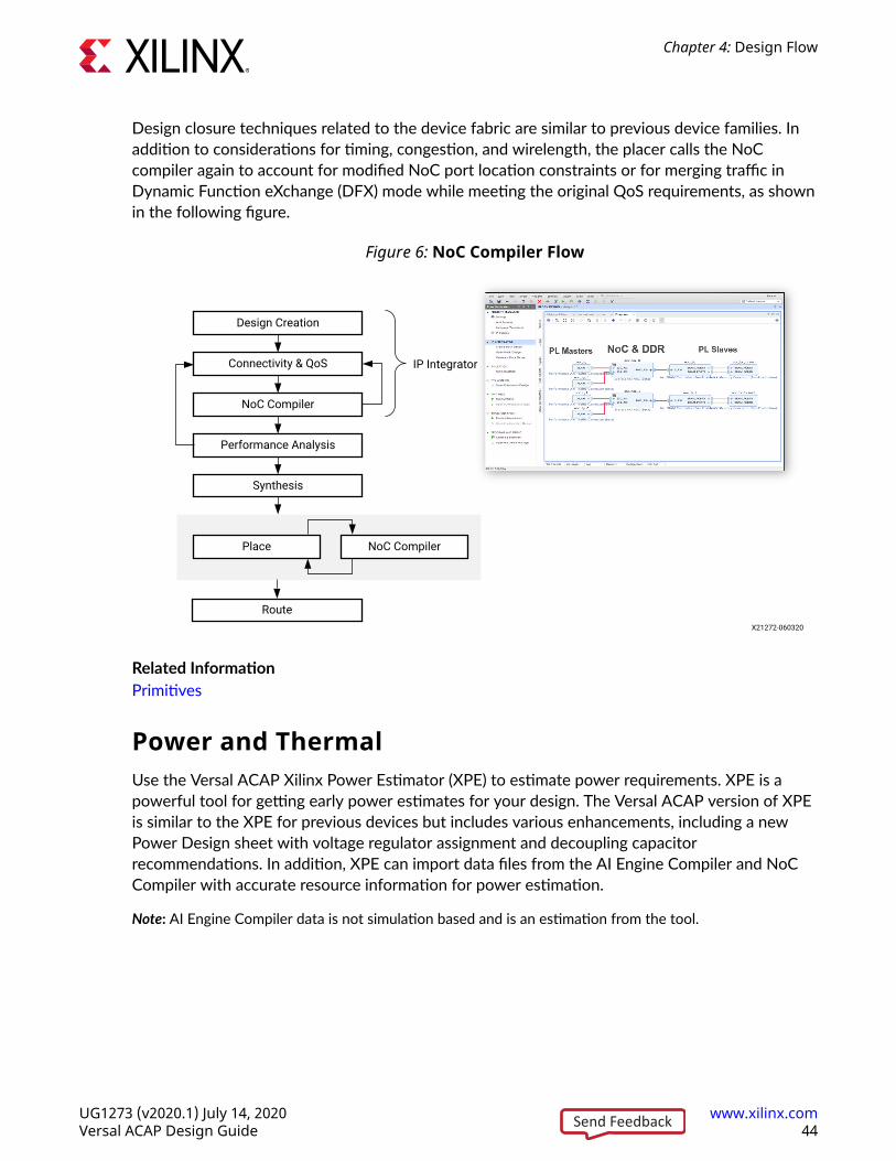
Design closure techniques related to the device fabric are similar to previous device families. Inaddition to considerations for timing, congestion, and wirelength, the placer calls the NoCcompiler again to account for modified NoC port location constraints or for merging traffic inDynamic Function eXchange (DFX) mode while meeting the original QoS requirements, as shownin the following figure.
Figure 6: NoC Compiler Flow
Design Creation
Connectivity & QoS
NoC Compiler
Performance Analysis
Synthesis
Place NoC Compiler
Route
IP Integrator
X21272-060320
Related InformationPrimitives
Power and ThermalUse the Versal ACAP Xilinx Power Estimator (XPE) to estimate power requirements. XPE is apowerful tool for getting early power estimates for your design. The Versal ACAP version of XPEis similar to the XPE for previous devices but includes various enhancements, including a newPower Design sheet with voltage regulator assignment and decoupling capacitorrecommendations. In addition, XPE can import data files from the AI Engine Compiler and NoCCompiler with accurate resource information for power estimation.
Note: AI Engine Compiler data is not simulation based and is an estimation from the tool.
Chapter 4: Design Flow
UG1273 (v2020.1) July 14, 2020 www.xilinx.comVersal ACAP Design Guide 44Send Feedback
Versal devices are available in both lidded and lidless packaging. Where possible, Xilinxrecommends lidless packaging, which offers an optimized thermal solution that minimizesthermal resistance and provides the most effective Theta Ja possible. From the XPE PowerDesign sheet, you can access Xilinx-provided thermal models that support Siemens SimcenterFlotherm and Ansys Icepac. For verified power delivery solutions for Versal ACAP, see the Powerpage on the Xilinx website.
I/O PlanningFor Versal ACAP, the I/O planning flow for high-performance I/O differs from previous devices,and the I/O planning flow for low-performance I/O (e.g., below 500 Mb/s) remains the same.
XPIO
The high-performance I/O in Versal ACAP is known as XPIO. The XPIO are located at the bottomperiphery of the device, unlike the columnar I/O architecture found in previous devices. XPIOports that exist below the PS on the left side of the device and below the GTs on the right side ofthe device are known as corner I/O. Corner I/O have limited use, such as for the integratedDDRMC and limited clocking. For more information on corner I/O, see the Versal ACAP Packagingand Pinouts Architecture Manual (AM013).
The XPIO provide XPHY logic that is similar to UltraScale™ device native mode. The XPHY logicencapsulates calibrated delays along with serialization and deserialization logic for 6 single-endedI/O ports known as nibble. Each XPIO bank contains 9 XPHY logic sites and allows for up to 54single-ended I/O ports. The XPHY logic is used for the integrated DDRMC, soft memorycontrollers, and any high-performance I/O interfaces.
IMPORTANT! Individual component mode cells, such as IDELAY, ODELAY, ISERDES, OSERDES, IDDR, andODDR, are eliminated for high-performance interfaces. The ISERDES and OSERDES primitives are notsupported in the Versal architecture, but similar functionality is supported through the XPHY logic.
Uncalibrated IDELAY, ODELAY, IDDR, and ODDR, known as I/O logic (IOL), exist in both XPIOand HDIO banks to support legacy low-performance interfaces operating at 500 Mb/s andbelow.
The I/O planning flow for high-performance interfaces is different from previous architecturesdue to the use of XPHY logic. If you previously generated high-performance interfaces using theXilinx Memory Interface Generator, High-Speed SelectIO wizard, or SelectIO component mode,you must rebuild the interfaces using Versal IP wizards.
The following table shows how the high-performance UltraScale device I/O generation maps tothe Versal device I/O generation.
Chapter 4: Design Flow
UG1273 (v2020.1) July 14, 2020 www.xilinx.comVersal ACAP Design Guide 45Send Feedback
Table 6: Device I/O Generation Comparison
UltraScale Device I/O Generation Versal ACAP I/O GenerationSoft memory controllers Integrated DDRMC via the Versal NoC IP
Soft memory controllers
High Speed SelectIO Wizard Versal Advanced I/O Wizard
UltraScale Component Mode
• High-performance interfaces
• Calibrated IDELAY, ODELAY, ISERDES, OSERDES, IDDR,and ODDR
Versal Advanced I/O Wizard
UltraScale Component Mode
• Low-performance interfaces (500 Mb/s and below)
• Uncalibrated IDELAY, ODELAY, IDDR, and ODDR
I/O logic instantiated in RTL
After you regenerate the IP for the Versal ACAP, you can perform I/O planning using theAdvanced I/O Planner, which is similar to soft memory controller I/O planning flow for UltraScaledevices. The Advanced I/O Planner guides you through the process of mapping your interfacesto the desired XPIO banks using the XPHY logic, ensuring that your high-speed interfaces arelegally mapped to the XPHY logic. For more information, see the Advanced I/O Wizard LogiCOREIP Product Guide (PG320).
Xilinx recommends I/O planning high-speed interfaces in the following order to achieve themaximum utilization of available XPHY logic resources:
1. Integrated DDRMC via NoC
2. Soft memory controllers
3. Advanced I/O wizard
4. I/O logic
For information, see the following documents:
• For DDR4 and LPDDR4 pinout rules, see the Versal ACAP Programmable Network on Chip andIntegrated Memory Controller LogiCORE IP Product Guide (PG313).
• For information on the Advanced I/O wizard, see the Versal ACAP SelectIO ResourcesArchitecture Manual (AM010).
High-Density I/O
The low-performance I/O in Versal ACAP are known as high-density I/O (HD I/O). The HD I/Osupport a subset of the UltraScale device component mode primitives through uncalibratedIDELAY, ODELAY, IDDR, and ODDR primitives known as I/O logic. HD I/O maintain thecolumnar I/O architecture found in previous devices.
Chapter 4: Design Flow
UG1273 (v2020.1) July 14, 2020 www.xilinx.comVersal ACAP Design Guide 46Send Feedback
The I/O planning flow for HD I/O is unchanged from previous architectures. You can continue toinstantiate the I/O logic primitives in your HDL code. The tools support an XDC-basedconstraints flow for assigning PACKAGE_PIN constraints. As with previous architectures, you candrag and drop from the I/O Ports window onto the Package window. In addition, you can moveI/O logic primitives between HD I/O banks and XPIO banks in the Versal ACAP.
IMPORTANT! The voltage ranges between XPIO and HD I/O do not overlap. XPIO supports a lower range ofvoltage than HD I/O.
ClockingThe Versal ACAP clocking architecture introduces some hardware improvements and changesfrom the UltraScale architecture. For detailed architecture information, see the Versal ACAPClocking Resources Architecture Manual (AM003).
Design ClosureThe Versal architecture introduces new hardware features that require additional considerationsto reach design closure, including timing and performance closure.
Simulation FlowsTo address the different needs in simulation scope, abstraction, and purpose, Xilinx providesdedicated flows for the various components of a Versal ACAP design, including the AI Engine, PS,and PL. The hardware emulation system simulation flow also allows for simulating the entiresystem in a single setup.
AI Engine SimulationAI Engine simulation tests code running on the Versal AI Engines. The scope of this simulation isan arbitrary number of AI Engine graphs and kernels, and you can include PL kernels inside thegraph modeled in C++ or SystemC. Two abstractions are supported, untimed and cycle-approximate, providing a trade-off between simulation speed and accuracy. The purpose of thissimulation is to verify the functional correctness of the code and to validate performance in astandalone context, independently of interactions with other functions.
AI Engine simulation is available through the Vitis unified software platform.
Chapter 4: Design Flow
UG1273 (v2020.1) July 14, 2020 www.xilinx.comVersal ACAP Design Guide 47Send Feedback
HLS SimulationHLS simulation exclusively tests HLS code and is an integral part of the HLS developmentprocess. The scope of this simulation is a single HLS kernel. Two abstractions are supported,untimed and RTL (cycle-accurate). These two abstractions are referred to as Csim and Cosimrespectively. In the Cosim flow, the output of RTL code generated by the HLS compiler isautomatically compared against the output of the original C code. The purpose of this flow is toverify the functional correctness of the RTL and to validate performance in a standalone context,independently of interactions with other functions.
HLS simulation is available through the Vitis unified software platform. For more information, seethe Vitis High-Level Synthesis User Guide (UG1399).
Embedded Software SimulationEmbedded software simulation tests a software design that targets only the PS. It is based on theQuick Emulator (QEMU), which emulates the behavior of the dual-core Arm® Cortex™-A72integrated in the Versal ACAP device. This simulation enables a fast, compact functionalvalidation of the platform OS. This flow includes a SystemC transaction-level model of thesystem, which allows for early system exploration and verification.
Embedded software simulation is available through the Vitis unified software platform.
Logic SimulationLogic simulation tests a hardware design targeting the PL fabric and is the traditional FPGAsimulation flow. The scope of this simulation is scalable, ranging from individual hardware blocksto the complete hardware platform. The simulated models are generally RTL, making theabstraction cycle-accurate. Simulation speed is proportional to the size of the test design, andlarger designs take comparatively longer to simulate. To improve simulation performance, you canreplace some Versal ACAP IP blocks with SystemC transaction-level models, which simulatefaster but are no longer be cycle-accurate. The purpose of this simulation is to verify and debugdetailed hardware functionality before implementing the design on the device.
Logic simulation is available through the Vivado Design Suite. For more information, see theVivado Design Suite User Guide: Logic Simulation (UG900).
Hardware EmulationHardware emulation simulates a complete Versal ACAP system composed of the AI Engine, PS,and PL. Using the Vitis software platform, you can integrate blocks and functions targeting allthree compute domains. The Vitis linker automatically generates a complete co-simulation setupinvolving RTL, SystemC, and QEMU models:
Chapter 4: Design Flow
UG1273 (v2020.1) July 14, 2020 www.xilinx.comVersal ACAP Design Guide 48Send Feedback
• Embedded software code running on the PS is emulated using QEMU.
• Code running on the AI Engines is emulated using the SystemC AI Engine simulator.
• User PL kernels are simulated as RTL code.
• IP blocks in the hardware platform are simulated either as RTL or SystemC TLM, based on thetypes of models available or selected.
As a result, the abstraction of the Vitis hardware emulation is very close to but not fully cycle-accurate. Some details of the Versal ACAP platform are abstracted with TLM models forsimulation speed purposes.
The scope of the Vitis hardware emulation also defines its purpose. Hardware emulation allowsyou to simulate the entire design and test the interactions between the PL, PS, and AI Engineprior to implementation. Because hardware emulation provides full debug visibility into allaspects of the application, it is easier to debug complex problems in this environment than in realhardware.
Hardware emulation is available through the Vitis unified software platform. For moreinformation, see Vitis Unified Software Platform Documentation: Application AccelerationDevelopment (UG1393).
Boot and ConfigurationVersal ACAPs have a centralized PMC subsystem responsible for the boot-up process, security,power management, and integrated debug. The Versal ACAP includes a separate power domainfor the PMC that must be powered and must perform boot-up prior to configuring the PL, NPI,and PS elements. Versal ACAP uses the BootROM and PLM for booting.
If you are migrating from UltraScale+™ device families, consider the following:
• UltraScale+ device designs: These devices contain integrated configuration logic that supportsa set of configuration modes on power-up. With Versal ACAP, there are changes to the bootand configuration flows.
• Zynq UltraScale+ MPSoC PS designs: Zynq® UltraScale+™ MPSoCs have a PMU and CSU tomanage and carry out the boot-up process. There are changes in the boot flow methodology.
Note: For more information, see the Versal ACAP Technical Reference Manual (AM011).
The following table compares the boot and configuration modes of UltraScale+ devices withVersal ACAP.
Chapter 4: Design Flow
UG1273 (v2020.1) July 14, 2020 www.xilinx.comVersal ACAP Design Guide 49Send Feedback
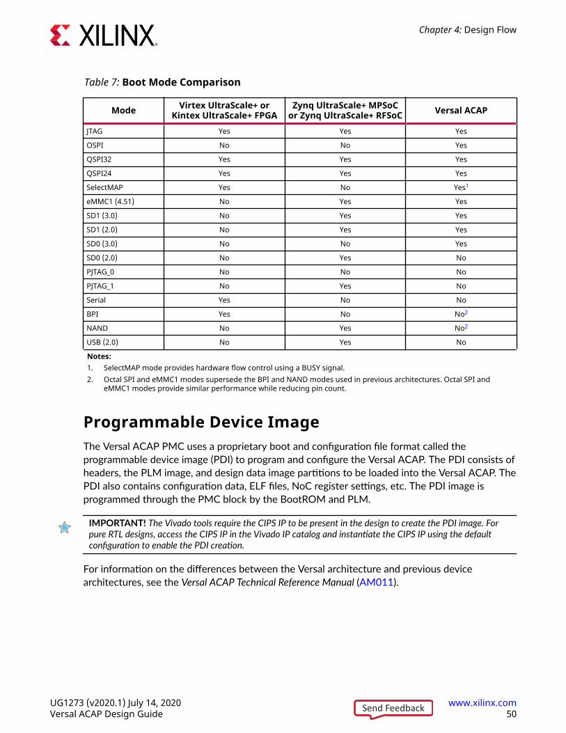
Table 7: Boot Mode Comparison
Mode Virtex UltraScale+ orKintex UltraScale+ FPGA
Zynq UltraScale+ MPSoCor Zynq UltraScale+ RFSoC Versal ACAP
JTAG Yes Yes Yes
OSPI No No Yes
QSPI32 Yes Yes Yes
QSPI24 Yes Yes Yes
SelectMAP Yes No Yes1
eMMC1 (4.51) No Yes Yes
SD1 (3.0) No Yes Yes
SD1 (2.0) No Yes Yes
SD0 (3.0) No No Yes
SD0 (2.0) No Yes No
PJTAG_0 No No No
PJTAG_1 No Yes No
Serial Yes No No
BPI Yes No No2
NAND No Yes No2
USB (2.0) No Yes No
Notes:1. SelectMAP mode provides hardware flow control using a BUSY signal.2. Octal SPI and eMMC1 modes supersede the BPI and NAND modes used in previous architectures. Octal SPI and
eMMC1 modes provide similar performance while reducing pin count.
Programmable Device ImageThe Versal ACAP PMC uses a proprietary boot and configuration file format called theprogrammable device image (PDI) to program and configure the Versal ACAP. The PDI consists ofheaders, the PLM image, and design data image partitions to be loaded into the Versal ACAP. ThePDI also contains configuration data, ELF files, NoC register settings, etc. The PDI image isprogrammed through the PMC block by the BootROM and PLM.
IMPORTANT! The Vivado tools require the CIPS IP to be present in the design to create the PDI image. Forpure RTL designs, access the CIPS IP in the Vivado IP catalog and instantiate the CIPS IP using the defaultconfiguration to enable the PDI creation.
For information on the differences between the Versal architecture and previous devicearchitectures, see the Versal ACAP Technical Reference Manual (AM011).
Chapter 4: Design Flow
UG1273 (v2020.1) July 14, 2020 www.xilinx.comVersal ACAP Design Guide 50Send Feedback
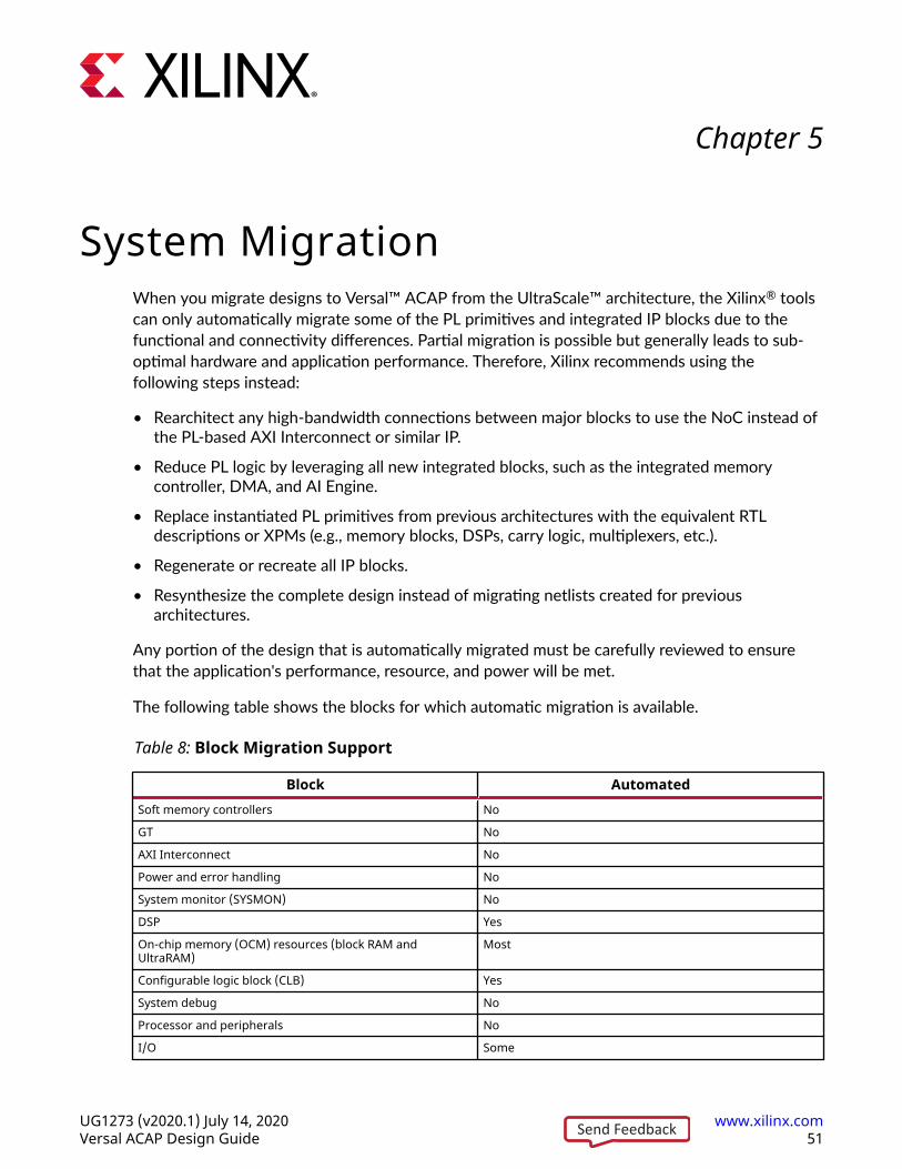
Chapter 5
System MigrationWhen you migrate designs to Versal™ ACAP from the UltraScale™ architecture, the Xilinx® toolscan only automatically migrate some of the PL primitives and integrated IP blocks due to thefunctional and connectivity differences. Partial migration is possible but generally leads to sub-optimal hardware and application performance. Therefore, Xilinx recommends using thefollowing steps instead:
• Rearchitect any high-bandwidth connections between major blocks to use the NoC instead ofthe PL-based AXI Interconnect or similar IP.
• Reduce PL logic by leveraging all new integrated blocks, such as the integrated memorycontroller, DMA, and AI Engine.
• Replace instantiated PL primitives from previous architectures with the equivalent RTLdescriptions or XPMs (e.g., memory blocks, DSPs, carry logic, multiplexers, etc.).
• Regenerate or recreate all IP blocks.
• Resynthesize the complete design instead of migrating netlists created for previousarchitectures.
Any portion of the design that is automatically migrated must be carefully reviewed to ensurethat the application's performance, resource, and power will be met.
The following table shows the blocks for which automatic migration is available.
Table 8: Block Migration Support
Block AutomatedSoft memory controllers No
GT No
AXI Interconnect No
Power and error handling No
System monitor (SYSMON) No
DSP Yes
On-chip memory (OCM) resources (block RAM andUltraRAM)
Most
Configurable logic block (CLB) Yes
System debug No
Processor and peripherals No
I/O Some
Chapter 5: System Migration
UG1273 (v2020.1) July 14, 2020 www.xilinx.comVersal ACAP Design Guide 51Send Feedback
Table 8: Block Migration Support (cont'd)
Block AutomatedPCIe subsystem Some
Tandem PCIe interfaces No
PL configuration and JTAG No
IMPORTANT! If your existing design contains blocks that are discontinued in Versal ACAP, you must manuallymigrate these blocks to a corresponding Versal ACAP block. For details, see the appropriate Versal ArchitectureManual.
For designs migrating from Kintex® UltraScale™ or Virtex® UltraScale™ devices, the CIPS IP mustbe added to enable essential functionality, such as device configuration and hardware debugfeatures. Other designs migrating from Zynq® UltraScale+™ MPSoCs are expected to alreadyhave a PS block.
Soft Memory ControllersIf your previous design used soft memory controller IP, you can either use the Versal ACAP softmemory controller IP or the integrated DDRMC. Xilinx recommends using the integratedDDRMC rather than using the Versal ACAP soft memory controller IP. In Versal ACAP, you canuse the integrated DDRMC only via the NoC. The NoC and DDRMC have very high bandwidthbut generally have a higher latency than a standalone soft memory controller. For some I/Obanks, only the integrated DDRMC is supported. For more information on the DDRMC, see theVersal Architecture and Product Data Sheet: Overview (DS950).
If you are using the soft memory controller IP, you must regenerate the IP for Versal ACAP. InVersal ACAP, an I/O bank comprises nine nibbles, and each nibble has six pins. Depending on thedevice and package, some I/O banks or some nibbles in an I/O bank are dedicated for theintegrated DDRMC. Soft memory controllers cannot use these dedicated pins. Pins dedicated forthe integrated DDRMC are designated as YES in the package file under the column namedDDRMC ONLY. The soft memory controllers can only use pins designated as NO.
Chapter 5: System Migration
UG1273 (v2020.1) July 14, 2020 www.xilinx.comVersal ACAP Design Guide 52Send Feedback
GTFor Versal ACAP, GT components are updated from Common/Channel to a quad granularity. Toenable some of the GT sharing use cases, GT wizard flows are modified to use the Vivado® IPintegrator. Use the Vivado IP integrator to build system designs and Advanced I/O planner to addphysical GT locations. This results in some manual migration effort for most of the non-Xilinx GT-based IP. When migrating your design, you must be aware of the full GT quad layout andsupported configuration options. For detailed architectural differences, see the Versal ACAP GTYTransceivers Architecture Manual (AM002).
AXI InterconnectThe soft IP AXI Interconnect is fully replaced by a combination of the integrated NoC resourcesand SmartConnect IP. When migrating your design, first consider using NoC resources for allmemory access pathways as well as to reduce PL resource utilization and support the high-bandwidth connections. You can then use SmartConnect to accommodate some conversionsonto the NoC or to offload traffic from a fully-utilized NoC network. When migrating your designto NoC resources, Xilinx strongly recommends using Vivado IP integrator for the instantiationand configuration of the NoC IP. For more information, see the Versal ACAP ProgrammableNetwork on Chip and Integrated Memory Controller LogiCORE IP Product Guide (PG313) andSmartConnect LogiCORE IP Product Guide (PG247).
Power and Error HandlingZynq UltraScale+ MPSoCs have some power modes that can be mapped to the power modes inVersal ACAP. Because the DDR is shared in the Versal ACAP, the DDR power modes, includingDDR self refresh and system power domain switching, are handled in the PLM. Zynq UltraScale+MPSoCs had error handling that was bound to the PS. In Versal ACAP, the PS handles its ownerrors but sends a summary to the PMC if action is required by the PMC. Errors from the DDR,PL, and SYSMON are handled by the PMC in Versal ACAP instead of the PS. For detailedarchitectural differences, see the Versal ACAP Technical Reference Manual (AM011).
Chapter 5: System Migration
UG1273 (v2020.1) July 14, 2020 www.xilinx.comVersal ACAP Design Guide 53Send Feedback
System MonitorThe Versal ACAP provides system monitoring capabilities similar to UltraScale+ devices. InUltraScale+ device designs you instantiated the SYSMON IP on the PL side and used the SystemManagement wizard to set up the register configuration for instantiation in the hardwaredescription language (HDL). In Versal ACAP, you configure the System Monitor settings in theCIPS IP core. To migrate your design, you must manually remove the SYSMON IP from thedesign. Xilinx recommends configuring the System Monitor using the CIPS IP. For moreinformation, see the Versal ACAP System Monitor Architecture Manual (AM006).
DSPThe Versal ACAP includes the DSP58 slice, which is a superset of and backward compatible withthe UltraScale+ device DSP48E2 slice. In addition, the Versal ACAP DSP Engine supports floatingpoint operations in a single DSP58 slice and can combine two back-to-back DSP58 slices withdedicated interconnect to build an 18-bit complex multiplier or complex multiply-accumulate(MACC). The DSPFP32 mode in Versal ACAP is supported through the Floating-Point OperatorIP. If you want to use this mode, update the Floating- Point Operator IP in your migrated design.
Xilinx supports automated migration of designs with DSP slices by inferring the appropriateinternal Versal ACAP legacy primitive (DSP48E5) for the DSP slices. Register-transfer level (RTL)instantiations are also automatically migrated. When migrating inferred code, Xilinx supportsautomatic migration using the same templates and resources. However, inference templates forprevious architectures do not automatically update to take advantage of the new modes ofoperation in the DSP58 (e.g., DSPCPLX). Xilinx recommends manual migration to take advantageof the new features in the Versal ACAP DSP58 slice for superior performance.
For detailed architectural differences, see the Versal ACAP DSP Engine Architecture Manual(AM004).
IMPORTANT! To take advantage of the Versal ACAP potential for increasing performance, consider whichparts of the datapath can be ported from the PL and into the AI Engines.
Related InformationDSP PrimitivesAI Engine
Chapter 5: System Migration
UG1273 (v2020.1) July 14, 2020 www.xilinx.comVersal ACAP Design Guide 54Send Feedback
On-Chip Memory ResourcesBlock RAM and UltraRAM used in designs from previous architectures are automatically migratedby inferring the appropriate Versal ACAP block. RTL instantiations are also automaticallymigrated. If certain block RAM and UltraRAM configurations are not supported in Versal ACAP, acritical warning message is issued and the instance is converted to a black box element. Thedesign must be changed to adhere to the supported configurations for Versal ACAP. Xilinxrecommends that you examine the configuration settings after design migration to ensure thecorrect defaults and settings were automatically selected. Xilinx recommends using Xilinxparameterizable macros (XPMs) to infer FIFOs and other memories. Integrated FIFOs are notsupported in Versal ACAP. In the Vivado IP integrator flow, the Embedded Memory Generatorand Embedded FIFO Generator replace the Block Memory Generator and FIFO Generator IP. Themigration for the Block Memory Generator and FIFO Generator IP is not automatic. For detailedarchitectural differences, see the Versal ACAP Memory Resources Architecture Manual (AM007).
Related InformationRAM Primitives
CLBCLBs in Versal ACAP have been enhanced from previous architectures. CLB resources that are nolonger supported in Versal ACAP (e.g., CARRY8, MUXF7, MUXF8, MUXF9, etc.) areautomatically migrated by inferring the appropriate Versal ACAP block. RTL instantiations arealso automatically migrated. For optimal area and timing results, Xilinx recommends that you donot instantiate CLB UNISIMs that are no longer supported in Versal ACAP and that you re-synthesize your RTL to infer the appropriate Versal ACAP block. For detailed architecturaldifferences, see the Versal ACAP Configurable Logic Block Architecture Manual (AM005).
Related InformationCLB Primitives
System DebugDebugging designs in PL fabric is similar to previous architectures, but there are several keydifferences:
• All fabric debug IP cores have AXI4-Stream slave control interfaces. Previous architecturesused a proprietary interface standard.
Chapter 5: System Migration
UG1273 (v2020.1) July 14, 2020 www.xilinx.comVersal ACAP Design Guide 55Send Feedback
• The debug hub IP core has both AXI4-Stream master control interfaces (for connection tofabric debug IP cores) and an AXI4-Memory Map slave interface for connection from the host.Debug hub IP in previous architectures relied on proprietary interfaces for connection to thedebug cores and host.
• The debug flows in the Vivado tools now support both automated and manual connectivitybetween debug hub and debug cores.
• The JTAG-to-AXI soft debug IP is no longer offered as an option in the Versal ACAParchitecture. The DAP and DPC can be used to access AXI-based blocks in your design.
• The AXI4-Stream-based integrated logic analyzer (ILA) core supports both ILA and System ILAfunctionality. In previous architectures, these were offered as separate IP cores.
When migrating, consider the following:
• Vivado IP integrator: You must manually remove or replace previously instantiated legacydebug cores. Replace the legacy debug cores with the new AXIS-ILA cores in the block designusing IP integrator.
• Netlist: Xilinx design constraints (XDC) commands for inserting ILA cores into the synthesizeddesign automatically migrate to the new AXIS-ILA debug IP.
• RTL: Due to the new interface requirements, the fabric debug cores from previousarchitectures are not automatically migrated to the new AXI4-Stream-based debug IP cores. Ifdebug cores from previous architectures are instantiated in the design, new debug IP must bemanually recustomized, regenerated, and reinstantiated in the design.
• IBERT and soft memory controller calibration: The integrated bit error ratio test (IBERT) IPfunctionality is part of the GT blocks and can be used with any design that uses thetransceivers. Memory controller calibration debug is available for both DDRMC blocks and forfabric-based soft memory controller IP.
• Debug Hub: Due to the new interface requirements, the legacy Debug Hub is automaticallyinserted into the netlist only if pl0_resetn is enabled on the CIPS. Alternatively, an AXI4Debug Hub can be manually added.
Chapter 5: System Migration
UG1273 (v2020.1) July 14, 2020 www.xilinx.comVersal ACAP Design Guide 56Send Feedback
Processor and PeripheralsSoftware stack for bare-metal applications and Linux applications on the PS in Versal ACAP aresimilar to Zynq UltraScale+ MPSoCs. Versal ACAP uses the PLM for booting. Zynq UltraScale+MPSoC designs that target the APU can be migrated to work with the Versal ACAP APU. TheVersal ACAP RPU uses the same Arm® Cortex™-R5F processor with the same GIC as ZynqUltraScale+ MPSoCs. The functionality and programming models are very similar. UltraScale+device designs that target the RPU can be migrated to work with the Versal ACAP RPU. Whenmigrating to Versal ACAP, you must take into consideration the device driver changes,multiplexed I/O (MIO) configuration, and pinouts. For more information, see the Versal ACAPTechnical Reference Manual (AM011).
I/OIDDR and ODDR are the only primitives that are automatically migrated.
Related InformationI/O Planning
PCIe SubsystemsThe Versal architecture includes several blocks for implementation of high performance,standards-based interfaces built on PCI™-SIG technologies. In addition to the CPM, the Versalarchitecture includes support for implementation of PCIe® interfaces in the PL. PL PCIe aresignificantly enhanced implementations of the integrated blocks for PCIe found in previousarchitectures. Two implementations of the PL PCIe exist: PL PCIE4 and PL PCIE5.
In Versal ACAPs with available PL PCIE4, the block is compliant with the PCIe Base SpecificationRevision 4.0 and capable of supporting defined line rates up to the maximum of 16 GT/s. DMA/Bridge subsystems for use with the PL PCIE4 are available through the Vivado IP catalog asadditional soft IP. PL PCIE4 does not provide CCIX support.
In Versal ACAPs with available PL PCIE5, the block is compliant with the PCIe Base SpecificationRevision 5.0 and capable of supporting defined line rates up to the maximum of 32 GT/s. DMA/Bridge subsystems for use with the PL PCIE5 are available through the Vivado IP catalog asadditional soft IP. CCIX support in PL PCIE5 complies with CCIX Base Specification Revision 1.1and enables solutions via additional soft IP.
Chapter 5: System Migration
UG1273 (v2020.1) July 14, 2020 www.xilinx.comVersal ACAP Design Guide 57Send Feedback
Previous designs that use the integrated blocks for PCIe are automatically migrated to VersalACAP PL PCIE4 or PL PCIE5. Therefore, most of the configuration selections and IP interfacesare compatible, and design migration is automated.
If your design needs to be migrated from an integrated block for PCIe in a previous architectureto a Versal architecture CPM, use the following methods:
• Configure the PCIe subsystem in the CPM using the CIPS IP core.
• Manually map the AXI4 memory-mapped (AXI4-MM) interfaces, including the AXI4-MMbridge, Xilinx DMA memory-mapped (XDMA-MM) interface, and queue DMA memory-mapped (QDMA-MM) interface, into the Versal ACAP NoC infrastructure. This requiressetting up various components in the design, such as the NoC, PS, address translation, andaddress allocation.
• Manually map RQ/RC/CQ/CC streaming, XDMA streaming, and QDMA streaming interfacesto Versal CPM PL interfaces. These interfaces are very similar to their respective IPimplementation from previous architectures.
Tandem PCIe configuration is different for Versal ACAP from previous architectures, becauseconfiguration occurs through the PMC rather than through the media configuration access port(MCAP) and internal configuration access port (ICAP). Currently, you must manually configurethese connections and settings in your design.
Xilinx recommends using the CPM, if available, as the primary PCIe interface for Versal ACAP.This block has hardened paths to the NoC infrastructure and resources, including the PMC, PS,and other management resources.
Tandem support for Versal ACAP devices is expected to include CPM-based Tandem PCIe, CPM-based Tandem PROM, CPM-based DFX over PCIe, and PL-based Tandem PROM. There are nocurrent plans to support Tandem PCIe for PL-based PCIe controllers.
Note: Additional support is planned to assist with migration for PCIe-based Tandem and Dynamic FunctioneXchange solutions.
For more information, see the following documents:
• Versal ACAP CPM CCIX Architecture Manual (AM016)
• Versal ACAP Integrated Block for PCI Express LogiCORE IP Product Guide (PG343)
• Versal ACAP PCIe PHY LogiCORE IP Product Guide (PG345)
• Versal ACAP CPM Mode for PCI Express Product Guide (PG346)
Related InformationCPM
Chapter 5: System Migration
UG1273 (v2020.1) July 14, 2020 www.xilinx.comVersal ACAP Design Guide 58Send Feedback
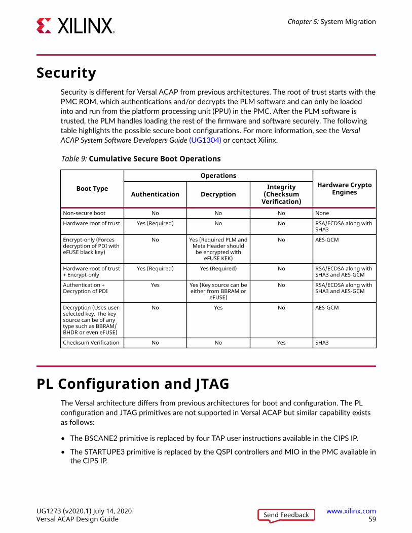
SecuritySecurity is different for Versal ACAP from previous architectures. The root of trust starts with thePMC ROM, which authentications and/or decrypts the PLM software and can only be loadedinto and run from the platform processing unit (PPU) in the PMC. After the PLM software istrusted, the PLM handles loading the rest of the firmware and software securely. The followingtable highlights the possible secure boot configurations. For more information, see the VersalACAP System Software Developers Guide (UG1304) or contact Xilinx.
Table 9: Cumulative Secure Boot Operations
Boot Type
OperationsHardware Crypto
EnginesAuthentication DecryptionIntegrity
(ChecksumVerification)
Non-secure boot No No No None
Hardware root of trust Yes (Required) No No RSA/ECDSA along withSHA3
Encrypt-only (Forcesdecryption of PDI witheFUSE black key)
No Yes (Required PLM andMeta Header should
be encrypted witheFUSE KEK)
No AES-GCM
Hardware root of trust+ Encrypt-only
Yes (Required) Yes (Required) No RSA/ECDSA along withSHA3 and AES-GCM
Authentication +Decryption of PDI
Yes Yes (Key source can beeither from BBRAM or
eFUSE)
No RSA/ECDSA along withSHA3 and AES-GCM
Decryption (Uses user-selected key. The keysource can be of anytype such as BBRAM/BHDR or even eFUSE)
No Yes No AES-GCM
Checksum Verification No No Yes SHA3
PL Configuration and JTAGThe Versal architecture differs from previous architectures for boot and configuration. The PLconfiguration and JTAG primitives are not supported in Versal ACAP but similar capability existsas follows:
• The BSCANE2 primitive is replaced by four TAP user instructions available in the CIPS IP.
• The STARTUPE3 primitive is replaced by the QSPI controllers and MIO in the PMC available inthe CIPS IP.
Chapter 5: System Migration
UG1273 (v2020.1) July 14, 2020 www.xilinx.comVersal ACAP Design Guide 59Send Feedback
• The DNA and EFUSE_USR are replaced by memory mapped AXI registers that can be read toget the device DNA or the user-programmable 32-bit eFUSE value. For more information,including address mapping, see the Versal ACAP Technical Reference Manual (AM011).
Chapter 5: System Migration
UG1273 (v2020.1) July 14, 2020 www.xilinx.comVersal ACAP Design Guide 60Send Feedback
Appendix A
PrimitivesThe Versal™ ACAP includes new primitives that the Vivado® synthesis tool infers.
Note: This appendix only covers the Versal ACAP primitives that differ from those in the UltraScale+™device families.
RAM PrimitivesThe Versal architecture supports both block RAM and UltraRAM primitives.
Block RAM PrimitivesFollowing are the block RAM primitives in Versal ACAP.
Primitives Supported Aspect Ratios Supported ModeRAMB36E5 1Kx36
2Kx184Kx9
x72 mode when running in simpledual-port (SDP) mode
RAMB18E5 1Kx182Kx9
x36 mode when running in SDP mode
In SDP mode, one address reads the RAM and the other address writes to the RAM. You can usedifferent clocks for the read and the write, but the address lines must be separate. The followingfigure shows an example.
Appendix A: Primitives
UG1273 (v2020.1) July 14, 2020 www.xilinx.comVersal ACAP Design Guide 61Send Feedback
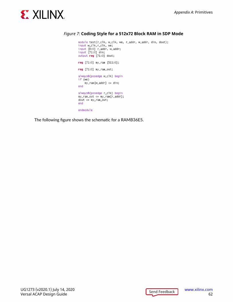
Figure 7: Coding Style for a 512x72 Block RAM in SDP Mode
The following figure shows the schematic for a RAMB36E5.
Appendix A: Primitives
UG1273 (v2020.1) July 14, 2020 www.xilinx.comVersal ACAP Design Guide 62Send Feedback
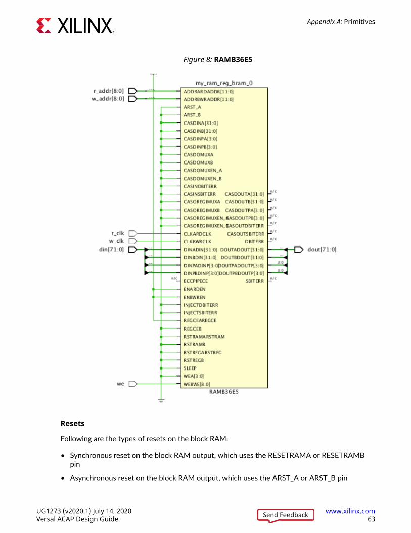
Figure 8: RAMB36E5
Resets
Following are the types of resets on the block RAM:
• Synchronous reset on the block RAM output, which uses the RESETRAMA or RESETRAMBpin
• Asynchronous reset on the block RAM output, which uses the ARST_A or ARST_B pin
Appendix A: Primitives
UG1273 (v2020.1) July 14, 2020 www.xilinx.comVersal ACAP Design Guide 63Send Feedback
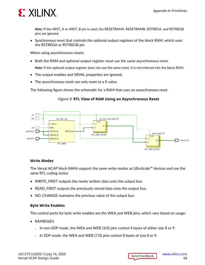
Note: If the ARST_A or ARST_B pin is used, the RESETRAMA, RESETRAMB, RSTREGA, and RSTREGBpins are ignored.
• Synchronous reset that controls the optional output registers of the block RAM, which usesthe RSTREGA or RSTREGB pin
When using asynchronous resets:
• Both the RAM and optional output register must use the same asynchronous reset.
Note: If the optional output register does not use the same reset, it is not inferred into the block RAM.
• The output enables and SRVAL properties are ignored.
• The asynchronous reset can only reset to a 0 value.
The following figure shows the schematic for a RAM that uses an asynchronous reset.
Figure 9: RTL View of RAM Using an Asynchronous Reset
Write Modes
The Versal ACAP block RAMs support the same write modes as UltraScale™ devices and use thesame RTL coding styles:
• WRITE_FIRST outputs the newly written data onto the output bus.
• READ_FIRST outputs the previously stored data onto the output bus.
• NO_CHANGE maintains the previous value of the output bus.
Byte Write Enables
The control ports for byte write enables are the WEA and WEB pins, which vary based on usage:
• RAMB36E5
○ In non-SDP mode, the WEA and WEB [3:0] pins control 4 bytes of either size 8 or 9.
○ In SDP mode, the WEA and WEB [7:0] pins control 8 bytes of size 8 or 9.
Appendix A: Primitives
UG1273 (v2020.1) July 14, 2020 www.xilinx.comVersal ACAP Design Guide 64Send Feedback
• RAMB18E5
○ In non-SDP mode, the WEA and WEB [1:0] pins control 2 bytes of size 8 or 9.
○ In SDP mode, pins WEA and WEB [3:0] pins control 4 bytes of 8 or 9.
Note: Size 9 names 8 bits with 1 parity bit.
Currently, Vivado synthesis only infers byte write RAM if sizes of 8 or 9 are used. In addition,Vivado synthesis only infers byte write enable RAM if the enables use one-hot state encoding.For example, in a byte write enabled RAM that is configured as true dual port with a data widthof 36, there are 4 different bytes, but only 1 byte can be written to at a time. To infer the blockRAM, make sure the RTL adheres to these restrictions.
Asymmetric RAMs
For asymmetric block RAMs in Versal ACAPs, use the same coding styles and rules that you usefor asymmetric block RAMs in UltraScale devices. For information on setting up asymmetricblock RAMs, see the Vivado Design Suite User Guide: Synthesis (UG901).
Note: Currently, Vivado synthesis does not support asynchronous reset on asymmetric block RAMs inVersal ACAPs.
UltraRAM PrimitivesFollowing is the UltraRAM primitive in Versal ACAPs. To instruct Vivado synthesis to infer theUltraRAM, you must set the RAM_STYLE = “ultra” attribute on the RAM.
Note: Like UltraScale devices, the UltraRAM for Versal ACAPs includes only one clock.
Primitive Supported Aspect Ratios Supported ModeURAM288E5 4Kx72
8Kx3616Kx1832Kx9
Dual portSingle port
Extra Registers
In addition to the optional output registers, the UltraRAM supports input registers on the datalines. As with block RAMs, you can reset the optional registers either with synchronous orasynchronous reset signals.
RAM Initialization
You can initialize the UltraRAMs using the INIT_xx attribute on the RAM as follows:
• Verilog: Use the readmemh command.
Appendix A: Primitives
UG1273 (v2020.1) July 14, 2020 www.xilinx.comVersal ACAP Design Guide 65Send Feedback
• VHDL: Set up a function to read an external file in VHDL.
For details, see the Vivado Design Suite User Guide: Synthesis (UG901).
Byte Write Enables
The UltraRAM also supports byte write enable operations. As with block RAMs, the bytes caneither be 8 bits or 9 bits using the extra parity bit. However, when using byte write with VersalACAPs, read operations are ignored during writing. Therefore, only the NO_CHANGE mode issupported when describing UltraRAMs with byte write.
Asymmetric UltraRAMs
Versal ACAP UltraRAMs support asymmetric aspect ratios. However, Vivado synthesis does notcurrently infer UltraRAMs in asymmetric mode.
DSP PrimitivesFollowing are the different types of DSP primitives for Versal ACAP.
Primitive Description UsageDSP58 Standard integer/Fixed point mode Inference or instantiation
DSPFP32 Floating point mode Instantiation only
DSPCPLX Complex multiplier Inference or instantiation
DSP58
For Versal ACAPs, the DSP58 primitive includes the same features as in UltraScale devices,including a multiplier, adder, pre-adder, and registers to fully pipeline the primitive. However,sizing differs and the primitives include additional features.
Sizing
For signed logic, you can configure DSP58 as follows:
• Multiplier: 27x24
• Adder: 58-bit
• Pre-adder: 27-bit
For unsigned logic, you can configure DSP58 as follows:
• Multiplier: 26x23
• Adder: 57-bit
Appendix A: Primitives
UG1273 (v2020.1) July 14, 2020 www.xilinx.comVersal ACAP Design Guide 66Send Feedback
• Pre-adder: 26-bit
The following figures show examples for signed logic.
Figure 10: RTL for a 27x24 Multiplier with 58-Bit Adder and 27-Bit Pre-Adder
Figure 11: Elaborated View of 27x24 Multiplier with 58-Bit Adder and 27-Bit Pre-Adder
Appendix A: Primitives
UG1273 (v2020.1) July 14, 2020 www.xilinx.comVersal ACAP Design Guide 67Send Feedback
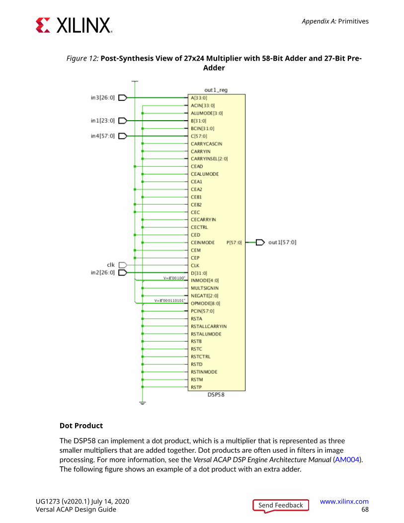
Figure 12: Post-Synthesis View of 27x24 Multiplier with 58-Bit Adder and 27-Bit Pre-Adder
Dot Product
The DSP58 can implement a dot product, which is a multiplier that is represented as threesmaller multipliers that are added together. Dot products are often used in filters in imageprocessing. For more information, see the Versal ACAP DSP Engine Architecture Manual (AM004).The following figure shows an example of a dot product with an extra adder.
Appendix A: Primitives
UG1273 (v2020.1) July 14, 2020 www.xilinx.comVersal ACAP Design Guide 68Send Feedback
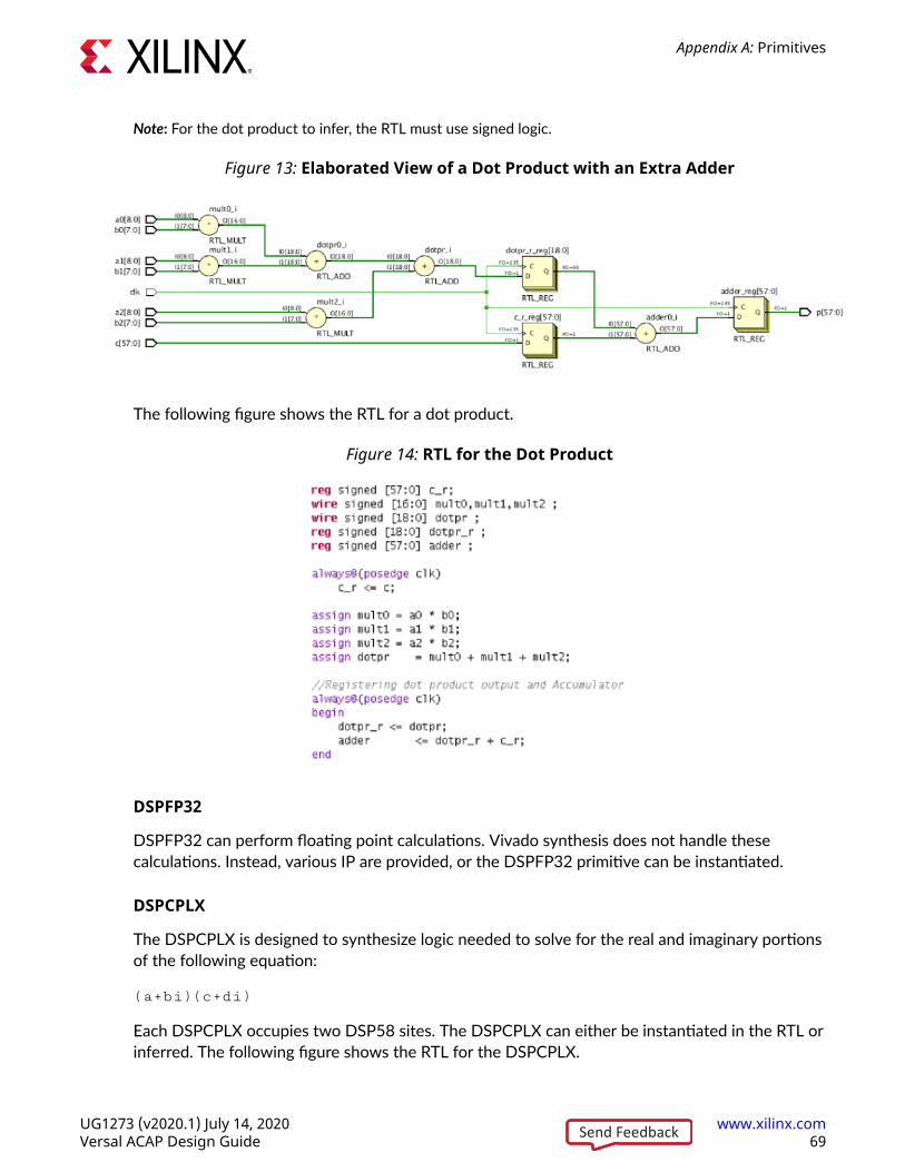
Note: For the dot product to infer, the RTL must use signed logic.
Figure 13: Elaborated View of a Dot Product with an Extra Adder
The following figure shows the RTL for a dot product.
Figure 14: RTL for the Dot Product
DSPFP32
DSPFP32 can perform floating point calculations. Vivado synthesis does not handle thesecalculations. Instead, various IP are provided, or the DSPFP32 primitive can be instantiated.
DSPCPLX
The DSPCPLX is designed to synthesize logic needed to solve for the real and imaginary portionsof the following equation:
(a+bi)(c+di)
Each DSPCPLX occupies two DSP58 sites. The DSPCPLX can either be instantiated in the RTL orinferred. The following figure shows the RTL for the DSPCPLX.
Appendix A: Primitives
UG1273 (v2020.1) July 14, 2020 www.xilinx.comVersal ACAP Design Guide 69Send Feedback
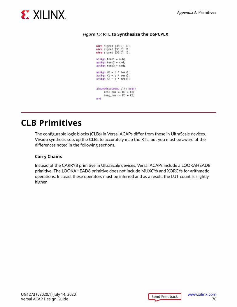
Figure 15: RTL to Synthesize the DSPCPLX
CLB PrimitivesThe configurable logic blocks (CLBs) in Versal ACAPs differ from those in UltraScale devices.Vivado synthesis sets up the CLBs to accurately map the RTL, but you must be aware of thedifferences noted in the following sections.
Carry Chains
Instead of the CARRY8 primitive in UltraScale devices, Versal ACAPs include a LOOKAHEAD8primitive. The LOOKAHEAD8 primitive does not include MUXCYs and XORCYs for arithmeticoperations. Instead, these operators must be inferred and as a result, the LUT count is slightlyhigher.
Appendix A: Primitives
UG1273 (v2020.1) July 14, 2020 www.xilinx.comVersal ACAP Design Guide 70Send Feedback
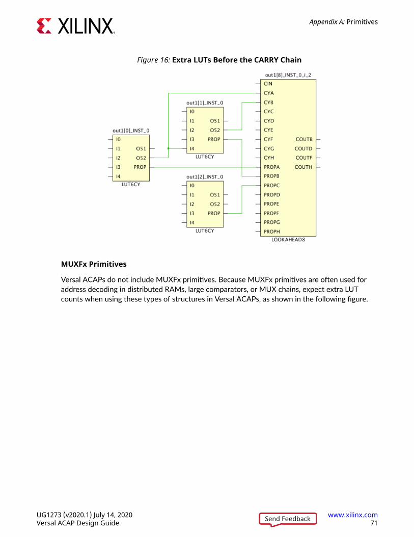
Figure 16: Extra LUTs Before the CARRY Chain
MUXFx Primitives
Versal ACAPs do not include MUXFx primitives. Because MUXFx primitives are often used foraddress decoding in distributed RAMs, large comparators, or MUX chains, expect extra LUTcounts when using these types of structures in Versal ACAPs, as shown in the following figure.
Appendix A: Primitives
UG1273 (v2020.1) July 14, 2020 www.xilinx.comVersal ACAP Design Guide 71Send Feedback
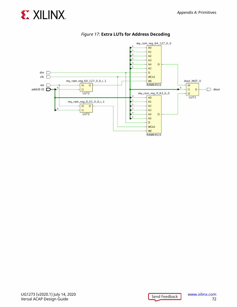
Figure 17: Extra LUTs for Address Decoding
Appendix A: Primitives
UG1273 (v2020.1) July 14, 2020 www.xilinx.comVersal ACAP Design Guide 72Send Feedback
Appendix B
Additional Resources and LegalNotices
Xilinx ResourcesFor support resources such as Answers, Documentation, Downloads, and Forums, see XilinxSupport.
Documentation Navigator and Design HubsXilinx® Documentation Navigator (DocNav) provides access to Xilinx documents, videos, andsupport resources, which you can filter and search to find information. To open DocNav:
• From the Vivado® IDE, select Help → Documentation and Tutorials.
• On Windows, select Start → All Programs → Xilinx Design Tools → DocNav.
• At the Linux command prompt, enter docnav.
Xilinx Design Hubs provide links to documentation organized by design tasks and other topics,which you can use to learn key concepts and address frequently asked questions. To access theDesign Hubs:
• In DocNav, click the Design Hubs View tab.
• On the Xilinx website, see the Design Hubs page.
Note: For more information on DocNav, see the Documentation Navigator page on the Xilinx website.
ReferencesThese documents provide supplemental material useful with this guide:
Appendix B: Additional Resources and Legal Notices
UG1273 (v2020.1) July 14, 2020 www.xilinx.comVersal ACAP Design Guide 73Send Feedback
1. Versal Architecture and Product Data Sheet: Overview (DS950)
2. Versal ACAP GTY Transceivers Architecture Manual (AM002)
3. Versal ACAP Clocking Resources Architecture Manual (AM003)
4. Versal ACAP DSP Engine Architecture Manual (AM004)
5. Versal ACAP Configurable Logic Block Architecture Manual (AM005)
6. Versal ACAP System Monitor Architecture Manual (AM006)
7. Versal ACAP Memory Resources Architecture Manual (AM007)
8. Versal ACAP AI Engine Architecture Manual (AM009)
9. Versal ACAP SelectIO Resources Architecture Manual (AM010)
10. Versal ACAP Technical Reference Manual (AM011)
11. Versal ACAP Packaging and Pinouts Architecture Manual (AM013)
12. Versal ACAP CPM CCIX Architecture Manual (AM016)
13. SmartConnect LogiCORE IP Product Guide (PG247)
14. Versal ACAP Programmable Network on Chip and Integrated Memory Controller LogiCORE IPProduct Guide (PG313)
15. Advanced I/O Wizard LogiCORE IP Product Guide (PG320)
16. Versal ACAP Integrated Block for PCI Express LogiCORE IP Product Guide (PG343)
17. Versal ACAP PCIe PHY LogiCORE IP Product Guide (PG345)
18. Versal ACAP CPM Mode for PCI Express Product Guide (PG346)
19. Vivado Design Suite User Guide: Logic Simulation (UG900)
20. Vivado Design Suite User Guide: Synthesis (UG901)
21. Vivado Design Suite User Guide: Designing IP Subsystems Using IP Integrator (UG994)
22. Vivado Design Suite: AXI Reference Guide (UG1037)
23. Versal ACAP System Software Developers Guide (UG1304)
24. Vitis Unified Software Platform Documentation: Application Acceleration Development (UG1393)
25. Vitis High-Level Synthesis User Guide (UG1399)
26. XRT Release Notes (UG1451)
27. RTL Kernels in the Application Acceleration Development flow of the Vitis Unified SoftwarePlatform Documentation (UG1416)
28. Vitis Unified Software Development Platform Documentation
Appendix B: Additional Resources and Legal Notices
UG1273 (v2020.1) July 14, 2020 www.xilinx.comVersal ACAP Design Guide 74Send Feedback
Please Read: Important Legal NoticesThe information disclosed to you hereunder (the "Materials") is provided solely for the selectionand use of Xilinx products. To the maximum extent permitted by applicable law: (1) Materials aremade available "AS IS" and with all faults, Xilinx hereby DISCLAIMS ALL WARRANTIES ANDCONDITIONS, EXPRESS, IMPLIED, OR STATUTORY, INCLUDING BUT NOT LIMITED TOWARRANTIES OF MERCHANTABILITY, NON-INFRINGEMENT, OR FITNESS FOR ANYPARTICULAR PURPOSE; and (2) Xilinx shall not be liable (whether in contract or tort, includingnegligence, or under any other theory of liability) for any loss or damage of any kind or naturerelated to, arising under, or in connection with, the Materials (including your use of theMaterials), including for any direct, indirect, special, incidental, or consequential loss or damage(including loss of data, profits, goodwill, or any type of loss or damage suffered as a result of anyaction brought by a third party) even if such damage or loss was reasonably foreseeable or Xilinxhad been advised of the possibility of the same. Xilinx assumes no obligation to correct anyerrors contained in the Materials or to notify you of updates to the Materials or to productspecifications. You may not reproduce, modify, distribute, or publicly display the Materialswithout prior written consent. Certain products are subject to the terms and conditions ofXilinx's limited warranty, please refer to Xilinx's Terms of Sale which can be viewed at https://www.xilinx.com/legal.htm#tos; IP cores may be subject to warranty and support terms containedin a license issued to you by Xilinx. Xilinx products are not designed or intended to be fail-safe orfor use in any application requiring fail-safe performance; you assume sole risk and liability foruse of Xilinx products in such critical applications, please refer to Xilinx's Terms of Sale which canbe viewed at https://www.xilinx.com/legal.htm#tos.
This document contains preliminary information and is subject to change without notice.Information provided herein relates to products and/or services not yet available for sale, andprovided solely for information purposes and are not intended, or to be construed, as an offer forsale or an attempted commercialization of the products and/or services referred to herein.
AUTOMOTIVE APPLICATIONS DISCLAIMER
AUTOMOTIVE PRODUCTS (IDENTIFIED AS "XA" IN THE PART NUMBER) ARE NOTWARRANTED FOR USE IN THE DEPLOYMENT OF AIRBAGS OR FOR USE IN APPLICATIONSTHAT AFFECT CONTROL OF A VEHICLE ("SAFETY APPLICATION") UNLESS THERE IS ASAFETY CONCEPT OR REDUNDANCY FEATURE CONSISTENT WITH THE ISO 26262AUTOMOTIVE SAFETY STANDARD ("SAFETY DESIGN"). CUSTOMER SHALL, PRIOR TO USINGOR DISTRIBUTING ANY SYSTEMS THAT INCORPORATE PRODUCTS, THOROUGHLY TESTSUCH SYSTEMS FOR SAFETY PURPOSES. USE OF PRODUCTS IN A SAFETY APPLICATIONWITHOUT A SAFETY DESIGN IS FULLY AT THE RISK OF CUSTOMER, SUBJECT ONLY TOAPPLICABLE LAWS AND REGULATIONS GOVERNING LIMITATIONS ON PRODUCTLIABILITY.
Appendix B: Additional Resources and Legal Notices
UG1273 (v2020.1) July 14, 2020 www.xilinx.comVersal ACAP Design Guide 75Send Feedback
Copyright
© Copyright 2020 Xilinx, Inc. Xilinx, the Xilinx logo, Alveo, Artix, Kintex, Spartan, Versal, Virtex,Vivado, Zynq, and other designated brands included herein are trademarks of Xilinx in the UnitedStates and other countries. AMBA, AMBA Designer, Arm, ARM1176JZ-S, CoreSight, Cortex,PrimeCell, Mali, and MPCore are trademarks of Arm Limited in the EU and other countries.OpenCL and the OpenCL logo are trademarks of Apple Inc. used by permission by Khronos. PCI,PCIe, and PCI Express are trademarks of PCI-SIG and used under license. All other trademarksare the property of their respective owners.
Appendix B: Additional Resources and Legal Notices
UG1273 (v2020.1) July 14, 2020 www.xilinx.comVersal ACAP Design Guide 76Send Feedback