Embed Size (px)
Citation preview
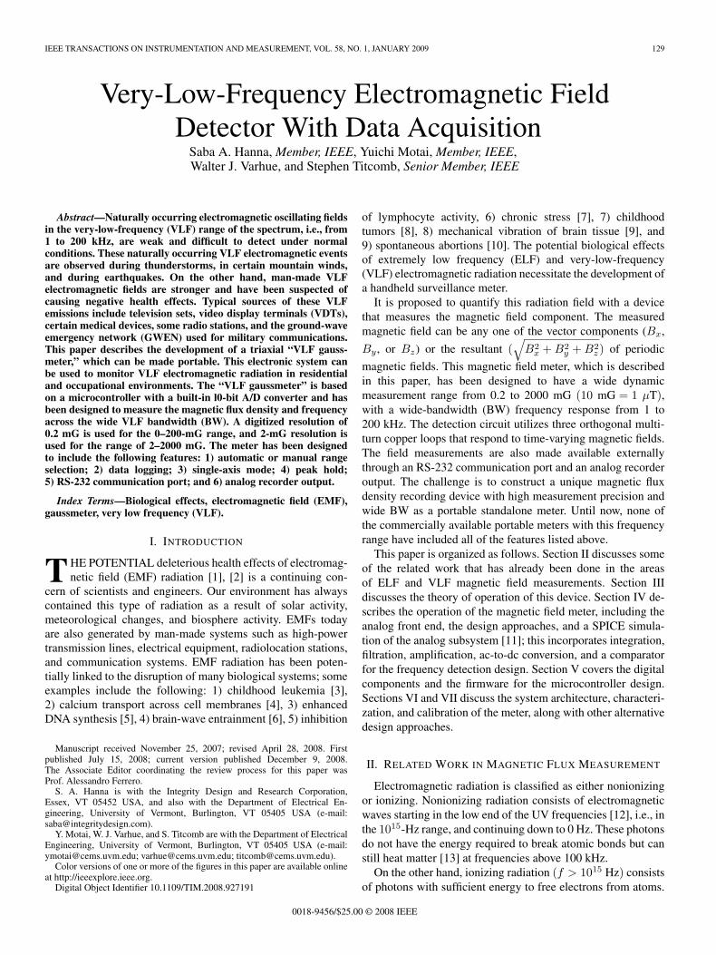
IEEE TRANSACTIONS ON INSTRUMENTATION AND MEASUREMENT, VOL. 58, NO. 1, JANUARY 2009 129
Very-Low-Frequency Electromagnetic FieldDetector With Data Acquisition
Saba A. Hanna, Member, IEEE, Yuichi Motai, Member, IEEE,Walter J. Varhue, and Stephen Titcomb, Senior Member, IEEE
Abstract—Naturally occurring electromagnetic oscillating fieldsin the very-low-frequency (VLF) range of the spectrum, i.e., from1 to 200 kHz, are weak and difficult to detect under normalconditions. These naturally occurring VLF electromagnetic eventsare observed during thunderstorms, in certain mountain winds,and during earthquakes. On the other hand, man-made VLFelectromagnetic fields are stronger and have been suspected ofcausing negative health effects. Typical sources of these VLFemissions include television sets, video display terminals (VDTs),certain medical devices, some radio stations, and the ground-waveemergency network (GWEN) used for military communications.This paper describes the development of a triaxial “VLF gauss-meter,” which can be made portable. This electronic system canbe used to monitor VLF electromagnetic radiation in residentialand occupational environments. The “VLF gaussmeter” is basedon a microcontroller with a built-in l0-bit A/D converter and hasbeen designed to measure the magnetic flux density and frequencyacross the wide VLF bandwidth (BW). A digitized resolution of0.2 mG is used for the 0–200-mG range, and 2-mG resolution isused for the range of 2–2000 mG. The meter has been designedto include the following features: 1) automatic or manual rangeselection; 2) data logging; 3) single-axis mode; 4) peak hold;5) RS-232 communication port; and 6) analog recorder output.
Index Terms—Biological effects, electromagnetic field (EMF),gaussmeter, very low frequency (VLF).
I. INTRODUCTION
THE POTENTIAL deleterious health effects of electromag-netic field (EMF) radiation [1], [2] is a continuing con-
cern of scientists and engineers. Our environment has alwayscontained this type of radiation as a result of solar activity,meteorological changes, and biosphere activity. EMFs todayare also generated by man-made systems such as high-powertransmission lines, electrical equipment, radiolocation stations,and communication systems. EMF radiation has been poten-tially linked to the disruption of many biological systems; someexamples include the following: 1) childhood leukemia [3],2) calcium transport across cell membranes [4], 3) enhancedDNA synthesis [5], 4) brain-wave entrainment [6], 5) inhibition
Manuscript received November 25, 2007; revised April 28, 2008. Firstpublished July 15, 2008; current version published December 9, 2008.The Associate Editor coordinating the review process for this paper wasProf. Alessandro Ferrero.
S. A. Hanna is with the Integrity Design and Research Corporation,Essex, VT 05452 USA, and also with the Department of Electrical En-gineering, University of Vermont, Burlington, VT 05405 USA (e-mail:[email protected]).
Y. Motai, W. J. Varhue, and S. Titcomb are with the Department of ElectricalEngineering, University of Vermont, Burlington, VT 05405 USA (e-mail:[email protected]; [email protected]; [email protected]).
Color versions of one or more of the figures in this paper are available onlineat http://ieeexplore.ieee.org.
Digital Object Identifier 10.1109/TIM.2008.927191
of lymphocyte activity, 6) chronic stress [7], 7) childhoodtumors [8], 8) mechanical vibration of brain tissue [9], and9) spontaneous abortions [10]. The potential biological effectsof extremely low frequency (ELF) and very-low-frequency(VLF) electromagnetic radiation necessitate the development ofa handheld surveillance meter.
It is proposed to quantify this radiation field with a devicethat measures the magnetic field component. The measuredmagnetic field can be any one of the vector components (Bx,
By, or Bz) or the resultant (√
B2x + B2
y + B2z) of periodic
magnetic fields. This magnetic field meter, which is describedin this paper, has been designed to have a wide dynamicmeasurement range from 0.2 to 2000 mG (10 mG = 1 μT),with a wide-bandwidth (BW) frequency response from 1 to200 kHz. The detection circuit utilizes three orthogonal multi-turn copper loops that respond to time-varying magnetic fields.The field measurements are also made available externallythrough an RS-232 communication port and an analog recorderoutput. The challenge is to construct a unique magnetic fluxdensity recording device with high measurement precision andwide BW as a portable standalone meter. Until now, none ofthe commercially available portable meters with this frequencyrange have included all of the features listed above.
This paper is organized as follows. Section II discusses someof the related work that has already been done in the areasof ELF and VLF magnetic field measurements. Section IIIdiscusses the theory of operation of this device. Section IV de-scribes the operation of the magnetic field meter, including theanalog front end, the design approaches, and a SPICE simula-tion of the analog subsystem [11]; this incorporates integration,filtration, amplification, ac-to-dc conversion, and a comparatorfor the frequency detection design. Section V covers the digitalcomponents and the firmware for the microcontroller design.Sections VI and VII discuss the system architecture, characteri-zation, and calibration of the meter, along with other alternativedesign approaches.
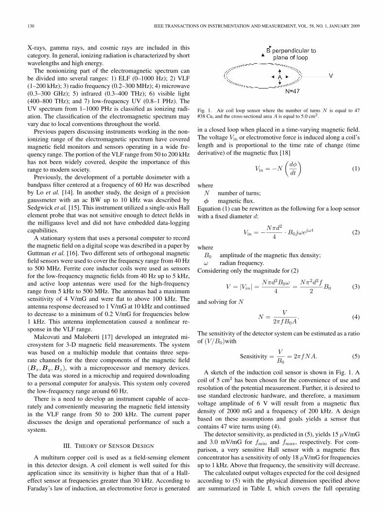
II. RELATED WORK IN MAGNETIC FLUX MEASUREMENT
Electromagnetic radiation is classified as either nonionizingor ionizing. Nonionizing radiation consists of electromagneticwaves starting in the low end of the UV frequencies [12], i.e., inthe 1015-Hz range, and continuing down to 0 Hz. These photonsdo not have the energy required to break atomic bonds but canstill heat matter [13] at frequencies above 100 kHz.
On the other hand, ionizing radiation (f > 1015 Hz) consistsof photons with sufficient energy to free electrons from atoms.
0018-9456/$25.00 © 2008 IEEE
130 IEEE TRANSACTIONS ON INSTRUMENTATION AND MEASUREMENT, VOL. 58, NO. 1, JANUARY 2009
X-rays, gamma rays, and cosmic rays are included in thiscategory. In general, ionizing radiation is characterized by shortwavelengths and high energy.
The nonionizing part of the electromagnetic spectrum canbe divided into several ranges: 1) ELF (0–1000 Hz); 2) VLF(1–200 kHz); 3) radio frequency (0.2–300 MHz); 4) microwave(0.3–300 GHz); 5) infrared (0.3–400 THz); 6) visible light(400–800 THz); and 7) low-frequency UV (0.8–1 PHz). TheUV spectrum from 1–1000 PHz is classified as ionizing radi-ation. The classification of the electromagnetic spectrum mayvary due to local conventions throughout the world.
Previous papers discussing instruments working in the non-ionizing range of the electromagnetic spectrum have coveredmagnetic field monitors and sensors operating in a wide fre-quency range. The portion of the VLF range from 50 to 200 kHzhas not been widely covered, despite the importance of thisrange to modern society.
Previously, the development of a portable dosimeter with abandpass filter centered at a frequency of 60 Hz was describedby Lo et al. [14]. In another study, the design of a precisiongaussmeter with an ac BW up to 10 kHz was described bySedgwick et al. [15]. This instrument utilized a single-axis Hallelement probe that was not sensitive enough to detect fields inthe milligauss level and did not have embedded data-loggingcapabilities.
A stationary system that uses a personal computer to recordthe magnetic field on a digital scope was described in a paper byGuttman et al. [16]. Two different sets of orthogonal magneticfield sensors were used to cover the frequency range from 40 Hzto 500 MHz. Ferrite core inductor coils were used as sensorsfor the low-frequency magnetic fields from 40 Hz up to 5 kHz,and active loop antennas were used for the high-frequencyrange from 5 kHz to 500 MHz. The antennas had a maximumsensitivity of 4 V/mG and were flat to above 100 kHz. Theantenna response decreased to 1 V/mG at 10 kHz and continuedto decrease to a minimum of 0.2 V/mG for frequencies below1 kHz. This antenna implementation caused a nonlinear re-sponse in the VLF range.
Malcovati and Maloberti [17] developed an integrated mi-crosystem for 3-D magnetic field measurements. The systemwas based on a multichip module that contains three sepa-rate channels for the three components of the magnetic field(Bx,By,Bz), with a microprocessor and memory devices.The data was stored in a microchip and required downloadingto a personal computer for analysis. This system only coveredthe low-frequency range around 60 Hz.
There is a need to develop an instrument capable of accu-rately and conveniently measuring the magnetic field intensityin the VLF range from 50 to 200 kHz. The current paperdiscusses the design and operational performance of such asystem.
III. THEORY OF SENSOR DESIGN
A multiturn copper coil is used as a field-sensing elementin this detector design. A coil element is well suited for thisapplication since its sensitivity is higher than that of a Hall-effect sensor at frequencies greater than 30 kHz. According toFaraday’s law of induction, an electromotive force is generated
Fig. 1. Air coil loop sensor where the number of turns N is equal to 47#38 Cu, and the cross-sectional area A is equal to 5.0 cm2.
in a closed loop when placed in a time-varying magnetic field.The voltage Vin or electromotive force is induced along a coil’slength and is proportional to the time rate of change (timederivative) of the magnetic flux [18]
Vin = −N
(dφ
dt
)(1)
whereN number of turns;φ magnetic flux.
Equation (1) can be rewritten as the following for a loop sensorwith a fixed diameter d:
Vin = −Nπd2
4· B0jωejωt (2)
whereB0 amplitude of the magnetic flux density;ω radian frequency.
Considering only the magnitude for (2)
V = |Vin| =Nπd2B0ω
4=
Nπ2d2f
2B0 (3)
and solving for N
N =V
2πfB0A. (4)
The sensitivity of the detector system can be estimated as a ratioof (V/B0)with
Sensitivity =V
B0= 2πfNA. (5)
A sketch of the induction coil sensor is shown in Fig. 1. Acoil of 5 cm2 has been chosen for the convenience of use andresolution of the potential measurement. Further, it is desired touse standard electronic hardware, and therefore, a maximumvoltage amplitude of 6 V will result from a magnetic fluxdensity of 2000 mG and a frequency of 200 kHz. A designbased on these assumptions and goals yields a sensor thatcontains 47 wire turns using (4).
The detector sensitivity, as predicted in (5), yields 15 μV/mGand 3.0 mV/mG for fmin and fmax, respectively. For com-parison, a very sensitive Hall sensor with a magnetic fluxconcentrator has a sensitivity of only 18 μV/mG for frequenciesup to 1 kHz. Above that frequency, the sensitivity will decrease.
The calculated output voltages expected for the coil designedaccording to (5) with the physical dimension specified aboveare summarized in Table I, which covers the full operating
HANNA et al.: VERY-LOW-FREQUENCY ELECTROMAGNETIC FIELD DETECTOR WITH DATA ACQUISITION 131
TABLE IEXPECTED OUTPUT VOLTAGES GENERATED BY THE COIL
USING DIFFERENT VALUES OF FREQUENCY
AND MAGNETIC FLUX DENSITY
range with minimum and maximum values for the frequencyand magnetic field strength.
IV. ANALOG SIGNAL PROCESSING
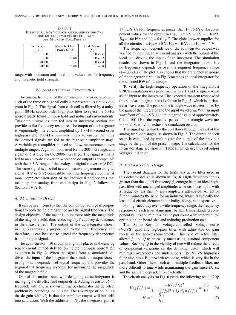
The analog front end of the sensor circuitry associated witheach of the three orthogonal coils is represented as a block dia-gram in Fig. 2. The signal from each coil is filtered by a unity-gain 100-Hz second-order high-pass filter to reject the 60-Hznoise usually found in household and industrial environments.This output signal is then fed into an integrator section thatprovides a flat frequency response. The output of the integratoris sequentially filtered and amplified by 100-Hz second-orderhigh-pass and 500-kHz low-pass filters to ensure that onlythe desired signals are fed to the high-gain amplifier stage.A variable-gain amplifier is used to allow measurements overmultiple ranges. A gain of 50 is used for the 200-mG range, anda gain of 5 is used for the 2000-mG range. The signal is finallyfed to an ac-to-dc converter, where the dc output is compatiblewith the 0–5-V range of the analog-to-digital converter (ADC).The same signal is also fed to a comparator to generate a digitalsignal (0 V or 5 V) compatible with the frequency counter. Amore complete discussion of the individual components thatmake up the analog front-end design in Fig. 2 follows inSections IV-A–E.
A. AC Integrator Design
It can be seen from (5) that the coil output voltage is propor-tional to both the field magnitude and the signal frequency. Thedesign objective of the meter is to measure only the magnitudeof the magnetic field, thus removing any frequency dependencein the measurement. The output of the ac integrator shownin Fig. 3 is inversely proportional to the input frequency, andtherefore, it can be used to cancel the frequency dependencefrom the input signal.
The ac integrator [19] shown in Fig. 3 is placed in the analogsensor circuit immediately following the high-pass noise filter,as shown in Fig. 2. When the signal from a simulated coildrives the input of the integrator, the simulated output shownin Fig. 4 is independent of signal frequency and provides therequired flat frequency response for measuring the magnitudeof the magnetic field.
One of the major issues with designing an ac integrator ismanaging the dc offset and output drift. Adding a resistor R2 infeedback with C1, as shown in Fig. 3, eliminates the dc offsetproblem by bounding the dc gain. The advantage of boundingthe dc gain with R2 is that the amplifier output will not driftinto saturation. With the addition of R2, the integrator gain is
1/(jωR1C1) for frequencies greater than 1/(R2C1). The com-ponent values for the circuit in Fig. 3 are R1 = R3 = 1.6 kΩ,R2 =160 kΩ, and C1 =0.01 μF. The global power supplies forall the circuits are Vcc =+9 V, Vee =−9 V, and Vdd =+5 V.
The frequency independence of the ac integrator output wasverified by running an ac circuit analysis with the output of theideal coil driving the input of the integrator. The simulationresults are shown in Fig. 4, and the integrator output hasno frequency dependence over the required frequency range(1–200 kHz). The plot also shows that the frequency responseof the integrator circuit in Fig. 3 matches an ideal integrator forthe selected BW of the design.
To verify the high-frequency operation of the integrator, aSPICE simulation was performed with a 100-kHz square waveas the input to the integrator. The expected transient response ofthis standard integrator test is shown in Fig. 5, which is a trian-gular waveform. The peak of the triangle wave is determined bythe gain of the integrator and the input waveform. With an inputwaveform of +/−5 V and an integrator gain of approximately0.1 at 100 kHz, the expected peaks of the triangle wave are+/−0.5 V, which matches the simulation results.
The signal generated by the coil flows through the rest of theanalog front-end stages, as shown in Fig. 2. The output of eachstage is calculated by multiplying the output of the previousstage by the gain of the present stage. The calculations for theintegrator stage are shown in Table II, which use the coil outputvoltages in Table I.
B. High-Pass Filter Design
The circuit diagram for the high-pass active filter used inthis detector design is shown in Fig. 6. High-frequency inputsgreater than the cutoff frequency f0 emerge from an ideal high-pass filter with unchanged amplitude, whereas those inputs witha frequency less than f0 are completely attenuated. An activefilter eliminates the need for an inductor, which is typically theleast ideal circuit element and is bulky, heavy, and expensive.
For high accuracy over a wide frequency range, the frequencyresponse of each filter stage must be flat. Using standard com-ponent values and minimizing the part count were important foroptimizing the board size and reducing production cost.
The Sallen–Key or voltage-controlled voltage-source(VCVS) quadratic high-pass filter with adjustable dc gainmeets all the above requirements. This type of active filterallows f0 and Q to be easily tuned using standard componentvalues. Keeping Q in the vicinity of one will reduce the effectsof component variations on the damping factor, which willminimize overshoots and undershoots. The VCVS high-passfilter also has a Butterworth response, which is very flat in thepass band. Other filters, such as a multiple-feedback filter, aremore difficult to tune while maintaining the gain since Q, f0,and the gain are dependent on each other.
The circuit analysis for Fig. 6 yields the following result [20]:
H(jf/f0) =−K(f/f0)2
1 − (f/f0)2 + (j/Q)(f/f0)=
V o
V i(6)
K = 1 +RB
RA(7)
132 IEEE TRANSACTIONS ON INSTRUMENTATION AND MEASUREMENT, VOL. 58, NO. 1, JANUARY 2009
Fig. 2. Block diagram for the analog front-end circuit design.
Fig. 3. AC integrator circuit schema.
Fig. 4. Frequency response for the ac integrator, coil, and integrator output.
Fig. 5. Integrator response at 100-kHz input frequency.
TABLE IICALCULATED OUTPUT VOLTAGE AT THE OUTPUT
STAGE OF THE INTEGRATOR
Fig. 6. Second-order high-pass filter circuit.
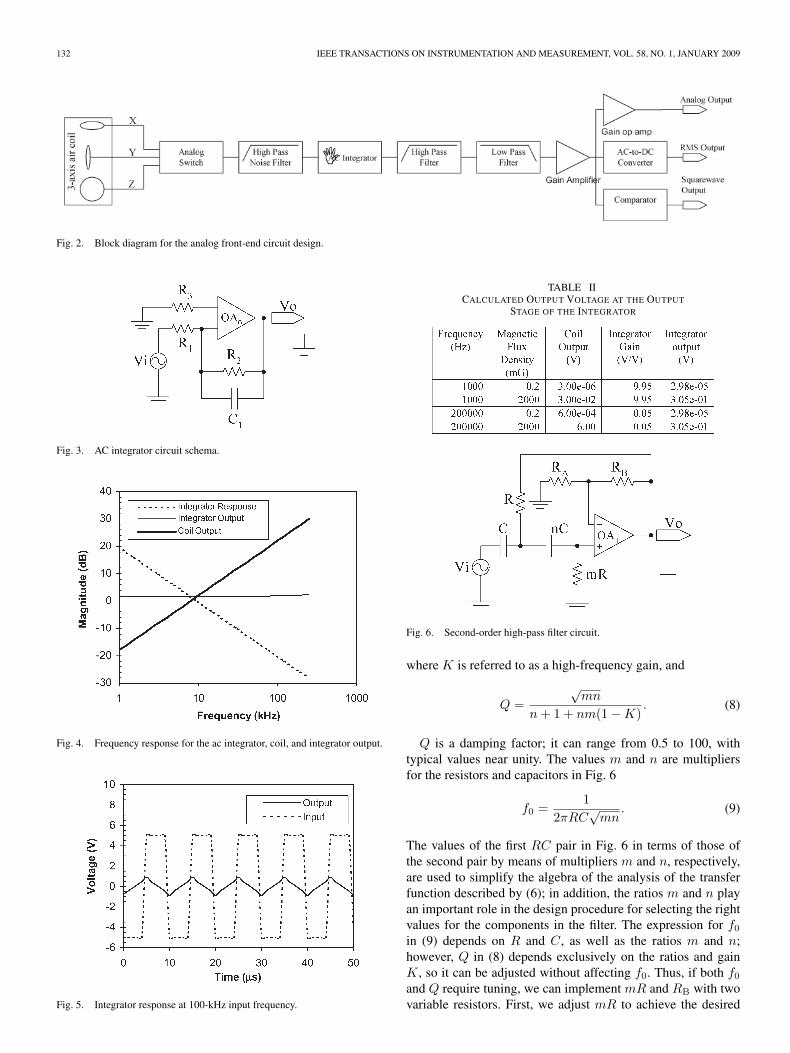
where K is referred to as a high-frequency gain, and
Q =√
mn
n + 1 + nm(1 − K). (8)
Q is a damping factor; it can range from 0.5 to 100, withtypical values near unity. The values m and n are multipliersfor the resistors and capacitors in Fig. 6
f0 =1
2πRC√
mn. (9)
The values of the first RC pair in Fig. 6 in terms of those ofthe second pair by means of multipliers m and n, respectively,are used to simplify the algebra of the analysis of the transferfunction described by (6); in addition, the ratios m and n playan important role in the design procedure for selecting the rightvalues for the components in the filter. The expression for f0
in (9) depends on R and C, as well as the ratios m and n;however, Q in (8) depends exclusively on the ratios and gainK, so it can be adjusted without affecting f0. Thus, if both f0
and Q require tuning, we can implement mR and RB with twovariable resistors. First, we adjust mR to achieve the desired
HANNA et al.: VERY-LOW-FREQUENCY ELECTROMAGNETIC FIELD DETECTOR WITH DATA ACQUISITION 133
Fig. 7. Ideal, first-, and second-order high-pass filter responses.
Fig. 8. Ideal (Q = 0.7), overdamped (Q = 0.43), and underdamped (Q =1.26) high-pass filter responses.
f0, which also affects Q, and then, we adjust RB to achieve thedesired Q, which does not affect f0.
A common task is to find suitable component values thatachieve a corner frequency f0 = 100 Hz with a gain of 4.65 dBand a damping factor of 1/
√2. The corner frequency (100 Hz)
is intentionally set lower than the desired cutoff frequency(1 kHz) for the wide bandpass filter to avoid the roll off near thecorner frequency and keep the frequency response linear. Thegain is set based on the system requirement of having a 0–5-Vsignal driving the ADC. The damping factor was selected tominimize the overshoot and undershoot of the high-pass filterresponse.
The component values chosen in this design are the fol-lowing: C = 47 nF, nC = 47 nF, R = 34 kΩ, mR = 34 kΩ,RA = 14 kΩ, and RB = 10 kΩ.
The simulation results for the second-order, first-order, andideal high-pass filters are shown in Fig. 7 with magnitudein decibels versus frequency. Note that the low-frequency as-ymptotic slope is 40 dB/dec for the second-order filter and20 dB/dec for the first-order filter. The sharper roll off of thesecond-order filter is closer to the ideal response, and thisproduces a more linear response near the cutoff frequency.The frequency response plot for different values of Q isshown in Fig. 8. Note that for low Q values, the transi-tion is very gradual, whereas for high Q values, there is arange of frequencies in the neighborhood of f0 = 100 Hz,where the magnitude is greater than the design goal of4.65 dB. The borderline between gradual (undershoot) andpeaked (overshoot) responses occurs when Q = 1/
√2. The
resulting curve is maximally flat and corresponds to a But-terworth filter response. Above 100 Hz, the response ap-proaches the flat response curve that is required for the desiredfilter BW.
Fig. 9. Second-order low-pass filter circuit design.
C. Low-Pass Filter Design
The circuit diagram for the low-pass active filter drawn inthe analog front-end block diagram is shown in Fig. 9. An ideallow-pass filter is characterized by the cutoff frequency f0, indi-cating that the sinusoidal inputs with a frequency less than f0
go through the filter with unchanged amplitude, whereas thosewith a frequency greater than f0 are completely attenuated.The design requirements for the low-pass filter are similar tothose of the high-pass filter described in Section IV-B. A VCVSquadratic low-pass active filter circuit with dc gain meets all theperformance and cost objectives.
The transfer function for the filter shown in Fig. 9 is given asfollows [20]:
H(jf/f0) =V o
V i=
K
1 − (f/f0)2 + (j/Q)(f/f0)(10)
where
K = 1 +RB
RA(11)
Q =√
mn
m + 1 + mn(1 − K)(12)
f0 =1
2πRC√
mn. (13)
For the same reasons that have already been discussed in thehigh-pass filter section, the ratios m and n in Fig. 9 providemore flexibility for choosing the desired component values ofthe circuit.
The design requires that suitable component values be identi-fied to obtain the desired values of f0, gain, and Q. This designrequires f0 = 900 kHz, gain = 8.5 dB, and Q = 1/
√2.
The component values chosen in this design are the fol-lowing: C = 0.01 nF, nC = 0.005 nF, R = 24.9 kΩ, mR =24.9 kΩ, RB = 20 kΩ, and RA = 12.1 kΩ.
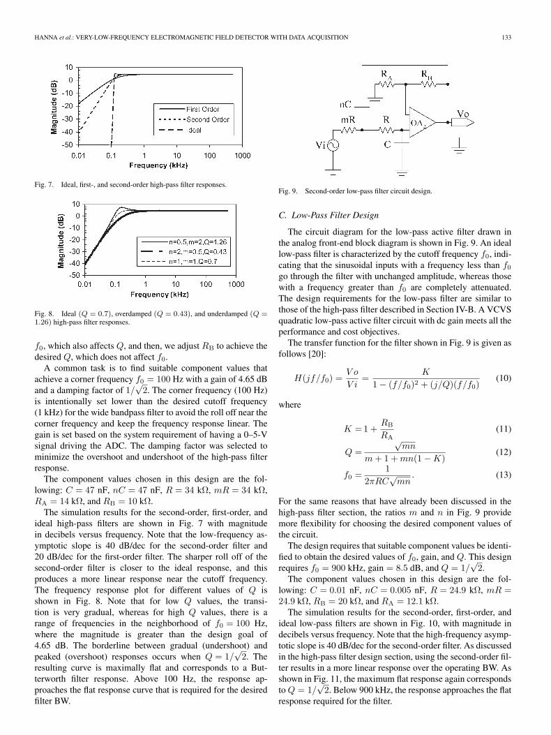
The simulation results for the second-order, first-order, andideal low-pass filters are shown in Fig. 10, with magnitude indecibels versus frequency. Note that the high-frequency asymp-totic slope is 40 dB/dec for the second-order filter. As discussedin the high-pass filter design section, using the second-order fil-ter results in a more linear response over the operating BW. Asshown in Fig. 11, the maximum flat response again correspondsto Q = 1/
√2. Below 900 kHz, the response approaches the flat
response required for the filter.
134 IEEE TRANSACTIONS ON INSTRUMENTATION AND MEASUREMENT, VOL. 58, NO. 1, JANUARY 2009
Fig. 10. Ideal, first-order, and second-order low-pass filter responses. Magni-tude (in decibels) versus frequency.
Fig. 11. Ideal (Q = 0.7), overdamped (Q = 0.47), and underdamped (Q =1.41) low-pass filter responses.
Fig. 12. Ideal, first-, and second-order wide-bandpass filter frequencyresponses.
The circuits in Figs. 6 and 9 are connected together, yieldinga second-order wide bandpass filter with maximum linearity,shown in Fig. 12. This figure also includes the first-orderand ideal filter responses for comparison. The flat frequencyresponse with a gain of 13.15 dB over the required BW for thisapplication is critical for accurate measurements through thefull frequency range of the meter, as shown in Fig. 13.
The signal generated by the integrator passes through thebandpass filter (combined high-pass and low-pass filters), asshown in Fig. 2. The expected output voltages of the bandpassfilter are shown in Table III, which uses the integrator outputvoltages in Table II.
Fig. 13. Ideal (Q = 0.7), overdamped (Q < 0.7), and underdamped (Q >0.7) wide bandpass filter responses.
TABLE IIIEXPECTED OUTPUT VOLTAGES OF THE BANDPASS FILTER
WITH A GAIN OF 13.15 dB
Fig. 14. Precision ac-to-dc converter.
D. AC-to-DC Converter Design
A ripple-free dc signal input is eventually required as theinput to the digital portion of this system design; therefore,the (ac) amplified signal is fed through an ac-to-dc converter.The precision ac-to-dc circuit used in this investigation is shownin Fig. 14. Its function with capacitor C2 removed from thecircuit is explained as follows. For negative input signals, thefirst operational amplifier (op-amp) OA3 is zero, and no currentflows through R3. The output of the second op-amp OA4 is
Eout = −R7
R6Ein. (14)
For positive input signals
Eout = R7
[Ein
R3− Ein
R6
]. (15)
If R3 = (1/2)R6, the output is (R7/R6)Ein; hence, theoutput is always the absolute value of the input.
Adding capacitor C2 across R7 causes op-amp OA4 to pro-duce an average pure dc output. The filter time constant R7C2
HANNA et al.: VERY-LOW-FREQUENCY ELECTROMAGNETIC FIELD DETECTOR WITH DATA ACQUISITION 135
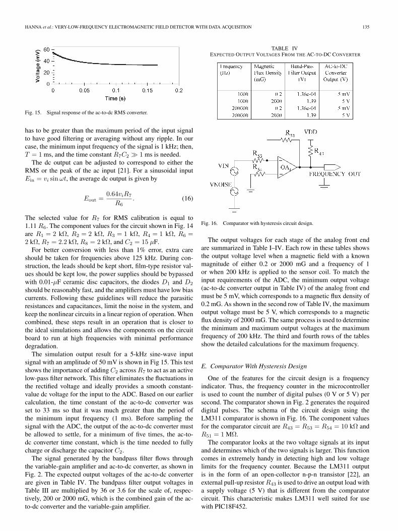
Fig. 15. Signal response of the ac-to-dc RMS converter.
has to be greater than the maximum period of the input signalto have good filtering or averaging without any ripple. In ourcase, the minimum input frequency of the signal is 1 kHz; then,T = 1 ms, and the time constant R7C2 � 1 ms is needed.
The dc output can be adjusted to correspond to either theRMS or the peak of the ac input [21]. For a sinusoidal inputEin = vi sin ωt, the average dc output is given by
Eout =0.64viR7
R6. (16)
The selected value for R7 for RMS calibration is equal to1.11 R6. The component values for the circuit shown in Fig. 14are R1 = 2 kΩ, R2 = 2 kΩ, R3 = 1 kΩ, R4 = 1 kΩ, R6 =2 kΩ, R7 = 2.2 kΩ, R8 = 2 kΩ, and C2 = 15 μF.
For better conversion with less than 1% error, extra careshould be taken for frequencies above 125 kHz. During con-struction, the leads should be kept short, film-type resistor val-ues should be kept low, the power supplies should be bypassedwith 0.01-μF ceramic disc capacitors, the diodes D1 and D2
should be reasonably fast, and the amplifiers must have low biascurrents. Following these guidelines will reduce the parasiticresistances and capacitances, limit the noise in the system, andkeep the nonlinear circuits in a linear region of operation. Whencombined, these steps result in an operation that is closer tothe ideal simulations and allows the components on the circuitboard to run at high frequencies with minimal performancedegradation.
The simulation output result for a 5-kHz sine-wave inputsignal with an amplitude of 50 mV is shown in Fig 15. This testshows the importance of adding C2 across R7 to act as an activelow-pass filter network. This filter eliminates the fluctuations inthe rectified voltage and ideally provides a smooth constant-value dc voltage for the input to the ADC. Based on our earliercalculation, the time constant of the ac-to-dc converter wasset to 33 ms so that it was much greater than the period ofthe minimum input frequency (1 ms). Before sampling thesignal with the ADC, the output of the ac-to-dc converter mustbe allowed to settle, for a minimum of five times, the ac-to-dc converter time constant, which is the time needed to fullycharge or discharge the capacitor C2.
The signal generated by the bandpass filter flows throughthe variable-gain amplifier and ac-to-dc converter, as shown inFig. 2. The expected output voltages of the ac-to-dc converterare given in Table IV. The bandpass filter output voltages inTable III are multiplied by 36 or 3.6 for the scale of, respec-tively, 200 or 2000 mG, which is the combined gain of the ac-to-dc converter and the variable-gain amplifier.
TABLE IVEXPECTED OUTPUT VOLTAGES FROM THE AC-TO-DC CONVERTER
Fig. 16. Comparator with hysteresis circuit design.
The output voltages for each stage of the analog front endare summarized in Table I–IV. Each row in these tables showsthe output voltage level when a magnetic field with a knownmagnitude of either 0.2 or 2000 mG and a frequency of 1or when 200 kHz is applied to the sensor coil. To match theinput requirements of the ADC, the minimum output voltage(ac-to-dc converter output in Table IV) of the analog front endmust be 5 mV, which corresponds to a magnetic flux density of0.2 mG. As shown in the second row of Table IV, the maximumoutput voltage must be 5 V, which corresponds to a magneticflux density of 2000 mG. The same process is used to determinethe minimum and maximum output voltages at the maximumfrequency of 200 kHz. The third and fourth rows of the tablesshow the detailed calculations for the maximum frequency.
E. Comparator With Hysteresis Design
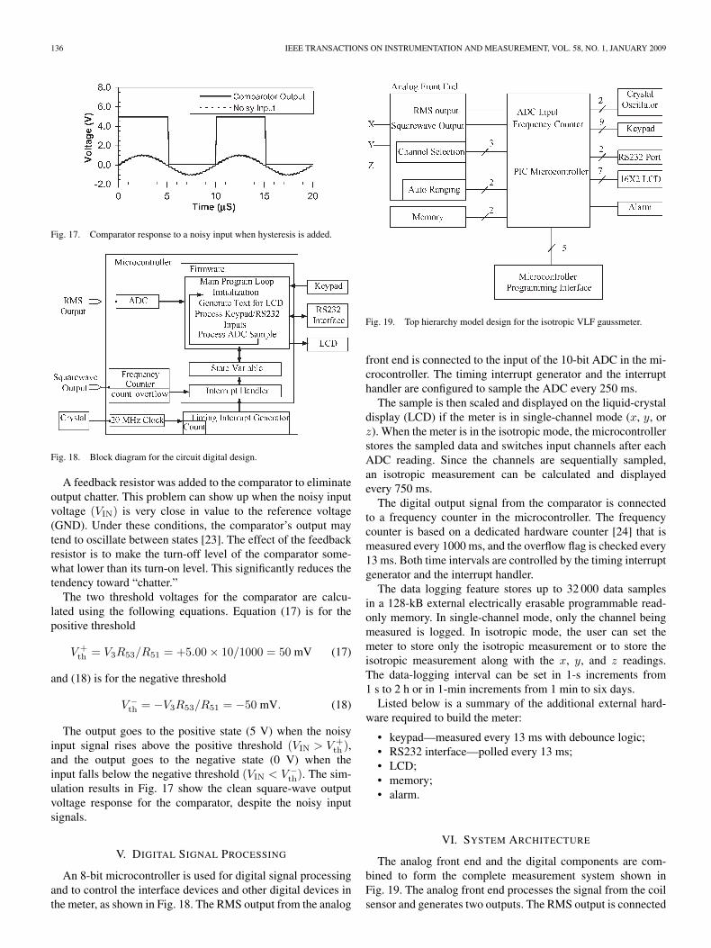
One of the features for the circuit design is a frequencyindicator. Thus, the frequency counter in the microcontrolleris used to count the number of digital pulses (0 V or 5 V) persecond. The comparator shown in Fig. 2 generates the requireddigital pulses. The schema of the circuit design using theLM311 comparator is shown in Fig. 16. The component valuesfor the comparator circuit are R43 = R53 = R54 = 10 kΩ andR51 = 1 MΩ.
The comparator looks at the two voltage signals at its inputand determines which of the two signals is larger. This functioncomes in extremely handy in detecting high and low voltagelimits for the frequency counter. Because the LM311 outputis in the form of an open-collector n-p-n transistor [22], anexternal pull-up resistor R43 is used to drive an output load witha supply voltage (5 V) that is different from the comparatorcircuit. This characteristic makes LM311 well suited for usewith PIC18F452.
136 IEEE TRANSACTIONS ON INSTRUMENTATION AND MEASUREMENT, VOL. 58, NO. 1, JANUARY 2009
Fig. 17. Comparator response to a noisy input when hysteresis is added.
Fig. 18. Block diagram for the circuit digital design.
A feedback resistor was added to the comparator to eliminateoutput chatter. This problem can show up when the noisy inputvoltage (VIN) is very close in value to the reference voltage(GND). Under these conditions, the comparator’s output maytend to oscillate between states [23]. The effect of the feedbackresistor is to make the turn-off level of the comparator some-what lower than its turn-on level. This significantly reduces thetendency toward “chatter.”
The two threshold voltages for the comparator are calcu-lated using the following equations. Equation (17) is for thepositive threshold
V +th = V3R53/R51 = +5.00 × 10/1000 = 50 mV (17)
and (18) is for the negative threshold
V −th = −V3R53/R51 = −50 mV. (18)
The output goes to the positive state (5 V) when the noisyinput signal rises above the positive threshold (VIN > V +
th ),and the output goes to the negative state (0 V) when theinput falls below the negative threshold (VIN < V −
th). The sim-ulation results in Fig. 17 show the clean square-wave outputvoltage response for the comparator, despite the noisy inputsignals.
V. DIGITAL SIGNAL PROCESSING
An 8-bit microcontroller is used for digital signal processingand to control the interface devices and other digital devices inthe meter, as shown in Fig. 18. The RMS output from the analog
Fig. 19. Top hierarchy model design for the isotropic VLF gaussmeter.
front end is connected to the input of the 10-bit ADC in the mi-crocontroller. The timing interrupt generator and the interrupthandler are configured to sample the ADC every 250 ms.
The sample is then scaled and displayed on the liquid-crystaldisplay (LCD) if the meter is in single-channel mode (x, y, orz). When the meter is in the isotropic mode, the microcontrollerstores the sampled data and switches input channels after eachADC reading. Since the channels are sequentially sampled,an isotropic measurement can be calculated and displayedevery 750 ms.
The digital output signal from the comparator is connectedto a frequency counter in the microcontroller. The frequencycounter is based on a dedicated hardware counter [24] that ismeasured every 1000 ms, and the overflow flag is checked every13 ms. Both time intervals are controlled by the timing interruptgenerator and the interrupt handler.
The data logging feature stores up to 32 000 data samplesin a 128-kB external electrically erasable programmable read-only memory. In single-channel mode, only the channel beingmeasured is logged. In isotropic mode, the user can set themeter to store only the isotropic measurement or to store theisotropic measurement along with the x, y, and z readings.The data-logging interval can be set in 1-s increments from1 s to 2 h or in 1-min increments from 1 min to six days.
Listed below is a summary of the additional external hard-ware required to build the meter:
• keypad—measured every 13 ms with debounce logic;• RS232 interface—polled every 13 ms;• LCD;• memory;• alarm.
VI. SYSTEM ARCHITECTURE
The analog front end and the digital components are com-bined to form the complete measurement system shown inFig. 19. The analog front end processes the signal from the coilsensor and generates two outputs. The RMS output is connected
HANNA et al.: VERY-LOW-FREQUENCY ELECTROMAGNETIC FIELD DETECTOR WITH DATA ACQUISITION 137
Fig. 20. Helmholtz coil for system-level testing.
to the ADC input for further digital signal processing, whereasthe square-wave output is connected to the frequency counter.
The microcontroller controls the channel selection based oninput from the user through the keypad or RS232 port. Thevariable gain amplifier in the analog front end is controlledby the range-selection signals from the microcontroller. Therange selection can be set manually, or the microcontroller candynamically select the range based on the measurements fromthe coil sensor.
VII. MAGNETIC FIELD METER PERFORMANCE
A. Helmholtz Coil Test Setup
The prototype development and calibration tests for the VLFgaussmeter’s field detection circuitry are performed with aHelmholtz coil, which is shown in Fig. 20, that provides aknown magnetic flux density as a function of the applied current[25], [26]. It is constructed with two parallel circular coilsspaced one radius apart and driven in phase. In our application,the current is adjusted to a value of 150 mA as we sweep thefrequencies to maintain a known magnetic field of 100 mG atthe center of the coil. The field at the center point A is given by
B =8μ0NI
53/2r= 0.00899
NI
r(19)
where B is in gauss, N is the number of turns, I is in amperes,and r is in meters.
The circuitry of the double-sided board used for developmentand the final verification tests is shown in Figs. 21 and 22.The digital components are on the top half of the board tomaximize the separation from the analog components that areon the bottom half. The circuit board is enclosed in a shieldedcase to reduce the sensitivity to external electromagnetic strayfields. The meter also filters out noise at frequencies outside thedesired BW.
B. Mechanical Arrangement of the 3-D Air Coil Sensor
The probe is constructed of three orthogonal nonconcentricair coils aligned so that their axes are mutually perpendicular,as shown in Fig. 23. The radius of each coil is 12.7 mm, and theoverall length of the probe is 65 mm.
C. Resonance Frequency Behavior
From an electrical circuit viewpoint, an individual air coilfrom the probe shown above is primarily an inductor repre-
Fig. 21. Development board—Component side.
Fig. 22. Development board—Solder side.
Fig. 23. Construction of a three-axis probe.
sented by the variable L. However, this inductor also con-tains some parasitic capacitance C and the coil winding re-sistance RW. Therefore, the behavior of this coil changes as
138 IEEE TRANSACTIONS ON INSTRUMENTATION AND MEASUREMENT, VOL. 58, NO. 1, JANUARY 2009
Fig. 24. Parallel resonant band-stop filter.
Fig. 25. Band-stop filter response with fr = 2800 kHz.
Fig. 26. Ideal and measured RMS magnetic field responses for the VLFgaussmeter versus frequency.
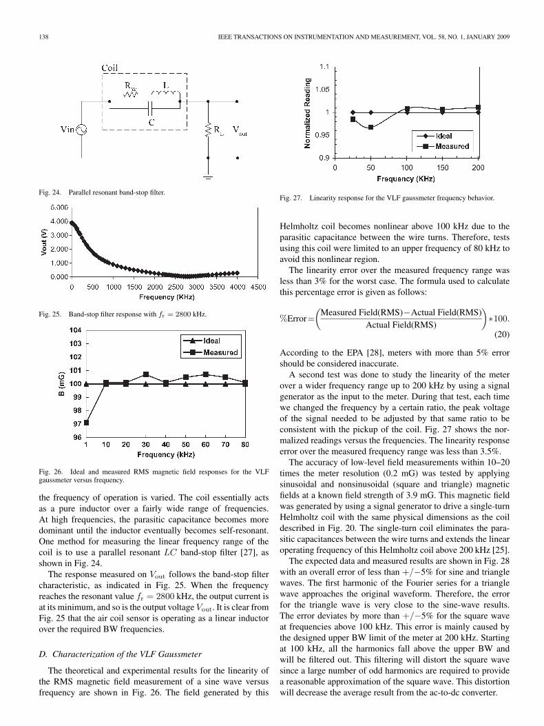
the frequency of operation is varied. The coil essentially actsas a pure inductor over a fairly wide range of frequencies.At high frequencies, the parasitic capacitance becomes moredominant until the inductor eventually becomes self-resonant.One method for measuring the linear frequency range of thecoil is to use a parallel resonant LC band-stop filter [27], asshown in Fig. 24.
The response measured on Vout follows the band-stop filtercharacteristic, as indicated in Fig. 25. When the frequencyreaches the resonant value fr = 2800 kHz, the output current isat its minimum, and so is the output voltage Vout. It is clear fromFig. 25 that the air coil sensor is operating as a linear inductorover the required BW frequencies.
D. Characterization of the VLF Gaussmeter
The theoretical and experimental results for the linearity ofthe RMS magnetic field measurement of a sine wave versusfrequency are shown in Fig. 26. The field generated by this
Fig. 27. Linearity response for the VLF gaussmeter frequency behavior.
Helmholtz coil becomes nonlinear above 100 kHz due to theparasitic capacitance between the wire turns. Therefore, testsusing this coil were limited to an upper frequency of 80 kHz toavoid this nonlinear region.
The linearity error over the measured frequency range wasless than 3% for the worst case. The formula used to calculatethis percentage error is given as follows:
%Error=(
Measured Field(RMS)−Actual Field(RMS)Actual Field(RMS)
)∗100.
(20)
According to the EPA [28], meters with more than 5% errorshould be considered inaccurate.
A second test was done to study the linearity of the meterover a wider frequency range up to 200 kHz by using a signalgenerator as the input to the meter. During that test, each timewe changed the frequency by a certain ratio, the peak voltageof the signal needed to be adjusted by that same ratio to beconsistent with the pickup of the coil. Fig. 27 shows the nor-malized readings versus the frequencies. The linearity responseerror over the measured frequency range was less than 3.5%.
The accuracy of low-level field measurements within 10–20times the meter resolution (0.2 mG) was tested by applyingsinusoidal and nonsinusoidal (square and triangle) magneticfields at a known field strength of 3.9 mG. This magnetic fieldwas generated by using a signal generator to drive a single-turnHelmholtz coil with the same physical dimensions as the coildescribed in Fig. 20. The single-turn coil eliminates the para-sitic capacitances between the wire turns and extends the linearoperating frequency of this Helmholtz coil above 200 kHz [25].
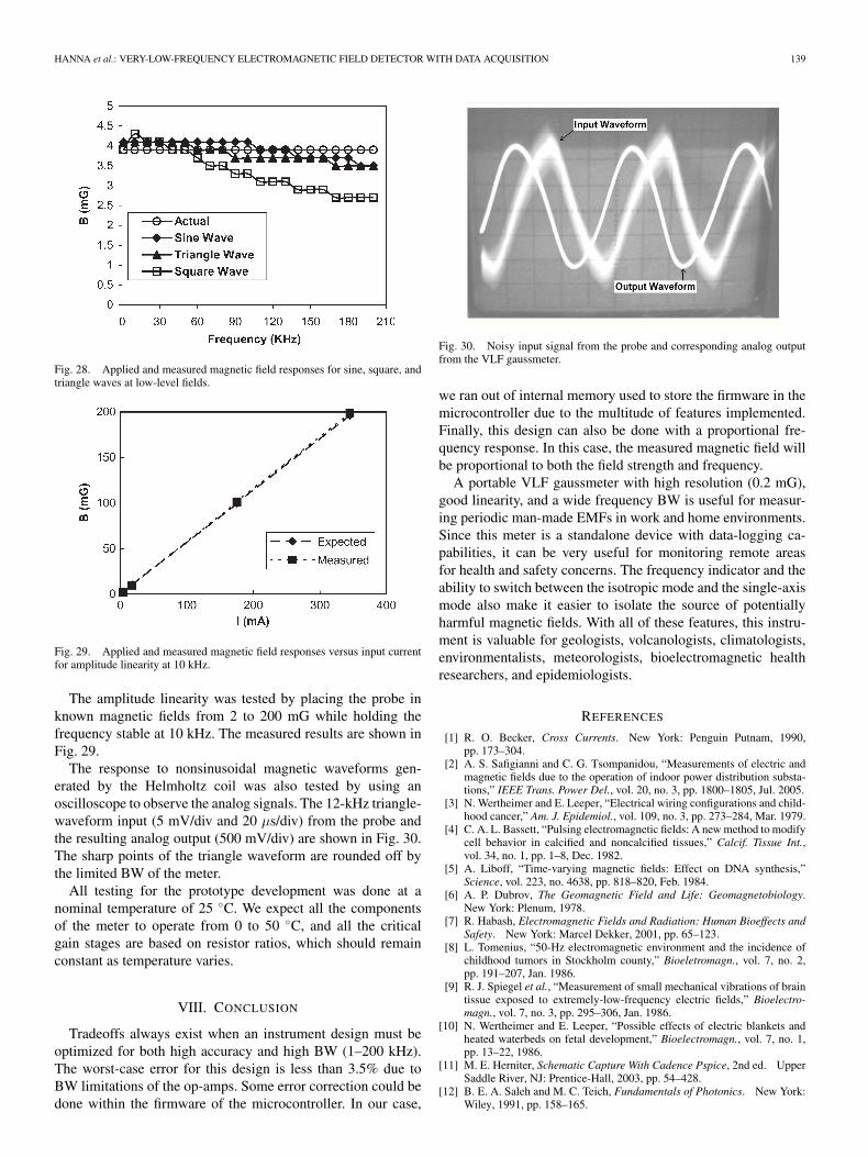
The expected data and measured results are shown in Fig. 28with an overall error of less than +/−5% for sine and trianglewaves. The first harmonic of the Fourier series for a trianglewave approaches the original waveform. Therefore, the errorfor the triangle wave is very close to the sine-wave results.The error deviates by more than +/−5% for the square waveat frequencies above 100 kHz. This error is mainly caused bythe designed upper BW limit of the meter at 200 kHz. Startingat 100 kHz, all the harmonics fall above the upper BW andwill be filtered out. This filtering will distort the square wavesince a large number of odd harmonics are required to providea reasonable approximation of the square wave. This distortionwill decrease the average result from the ac-to-dc converter.
HANNA et al.: VERY-LOW-FREQUENCY ELECTROMAGNETIC FIELD DETECTOR WITH DATA ACQUISITION 139
Fig. 28. Applied and measured magnetic field responses for sine, square, andtriangle waves at low-level fields.
Fig. 29. Applied and measured magnetic field responses versus input currentfor amplitude linearity at 10 kHz.
The amplitude linearity was tested by placing the probe inknown magnetic fields from 2 to 200 mG while holding thefrequency stable at 10 kHz. The measured results are shown inFig. 29.
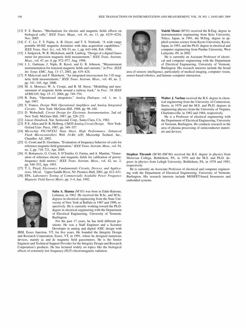
The response to nonsinusoidal magnetic waveforms gen-erated by the Helmholtz coil was also tested by using anoscilloscope to observe the analog signals. The 12-kHz triangle-waveform input (5 mV/div and 20 μs/div) from the probe andthe resulting analog output (500 mV/div) are shown in Fig. 30.The sharp points of the triangle waveform are rounded off bythe limited BW of the meter.
All testing for the prototype development was done at anominal temperature of 25 ◦C. We expect all the componentsof the meter to operate from 0 to 50 ◦C, and all the criticalgain stages are based on resistor ratios, which should remainconstant as temperature varies.
VIII. CONCLUSION
Tradeoffs always exist when an instrument design must beoptimized for both high accuracy and high BW (1–200 kHz).The worst-case error for this design is less than 3.5% due toBW limitations of the op-amps. Some error correction could bedone within the firmware of the microcontroller. In our case,
Fig. 30. Noisy input signal from the probe and corresponding analog outputfrom the VLF gaussmeter.
we ran out of internal memory used to store the firmware in themicrocontroller due to the multitude of features implemented.Finally, this design can also be done with a proportional fre-quency response. In this case, the measured magnetic field willbe proportional to both the field strength and frequency.
A portable VLF gaussmeter with high resolution (0.2 mG),good linearity, and a wide frequency BW is useful for measur-ing periodic man-made EMFs in work and home environments.Since this meter is a standalone device with data-logging ca-pabilities, it can be very useful for monitoring remote areasfor health and safety concerns. The frequency indicator and theability to switch between the isotropic mode and the single-axismode also make it easier to isolate the source of potentiallyharmful magnetic fields. With all of these features, this instru-ment is valuable for geologists, volcanologists, climatologists,environmentalists, meteorologists, bioelectromagnetic healthresearchers, and epidemiologists.
REFERENCES
[1] R. O. Becker, Cross Currents. New York: Penguin Putnam, 1990,pp. 173–304.
[2] A. S. Safigianni and C. G. Tsompanidou, “Measurements of electric andmagnetic fields due to the operation of indoor power distribution substa-tions,” IEEE Trans. Power Del., vol. 20, no. 3, pp. 1800–1805, Jul. 2005.
[3] N. Wertheimer and E. Leeper, “Electrical wiring configurations and child-hood cancer,” Am. J. Epidemiol., vol. 109, no. 3, pp. 273–284, Mar. 1979.
[4] C. A. L. Bassett, “Pulsing electromagnetic fields: A new method to modifycell behavior in calcified and noncalcified tissues,” Calcif. Tissue Int.,vol. 34, no. 1, pp. 1–8, Dec. 1982.
[5] A. Liboff, “Time-varying magnetic fields: Effect on DNA synthesis,”Science, vol. 223, no. 4638, pp. 818–820, Feb. 1984.
[6] A. P. Dubrov, The Geomagnetic Field and Life: Geomagnetobiology.New York: Plenum, 1978.
[7] R. Habash, Electromagnetic Fields and Radiation: Human Bioeffects andSafety. New York: Marcel Dekker, 2001, pp. 65–123.
[8] L. Tomenius, “50-Hz electromagnetic environment and the incidence ofchildhood tumors in Stockholm county,” Bioeletromagn., vol. 7, no. 2,pp. 191–207, Jan. 1986.
[9] R. J. Spiegel et al., “Measurement of small mechanical vibrations of braintissue exposed to extremely-low-frequency electric fields,” Bioelectro-magn., vol. 7, no. 3, pp. 295–306, Jan. 1986.
[10] N. Wertheimer and E. Leeper, “Possible effects of electric blankets andheated waterbeds on fetal development,” Bioelectromagn., vol. 7, no. 1,pp. 13–22, 1986.
[11] M. E. Herniter, Schematic Capture With Cadence Pspice, 2nd ed. UpperSaddle River, NJ: Prentice-Hall, 2003, pp. 54–428.
[12] B. E. A. Saleh and M. C. Teich, Fundamentals of Photonics. New York:Wiley, 1991, pp. 158–165.
140 IEEE TRANSACTIONS ON INSTRUMENTATION AND MEASUREMENT, VOL. 58, NO. 1, JANUARY 2009
[13] F. S. Barnes, “Mechanisms for electric and magnetic fields effects onbiological cells,” IEEE Trans. Magn., vol. 41, no. 11, pp. 4219–4224,Nov. 2005.
[14] C. C. Lo, T. Y. Fujita, A. B. Geyer, and T. S. Tenforde, “A wide rangeportable 60-HZ magnetic dosimeter with data acquisition capabilities,”IEEE Trans. Nucl. Sci., vol. NS-33, no. 1, pp. 643–646, Feb. 1986.
[15] J. Sedgwick, W. R. Michalson, and R. Ludwig, “Design of a digital Gaussmeter for precision magnetic field measurement,” IEEE Trans. Instrum.Meas., vol. 47, no. 4, pp. 972–977, Aug. 1998.
[16] J. L. Guttman, J. Niple, R. Kavet, and G. B. Johnson, “Measurementinstrumentation for transient magnetic fields and currents,” in Proc. IEEEInt. Symp. EMC, Aug. 13–17, 2001, pp. 419–424.
[17] P. Malcovati and F. Maloberti, “An integrated microsystem for 3-D mag-netic field measurements,” IEEE Trans. Instrum. Meas., vol. 49, no. 2,pp. 341–345, Apr. 2000.
[18] M. A. Moresco, W. A. Cronje, and B. M. Steyn, “Modelling and mea-surement of magnetic fields around a railway track,” in Proc. 7th IEEEAFRICON, Sep. 15–17, 2004, pp. 749–754.
[19] R. Stata, “Operational integrators,” Analog Dialogue, vol. 1, no. 1,Apr. 1967.
[20] S. Franco, Design With Operational Amplifiers and Analog IntegratedCircuits. New York: McGraw-Hill, 1988, pp. 96–160.
[21] D. Wobschall, Circuit Design for Electronic Instrumentation, 2nd ed.New York: McGraw-Hill, 1987, pp. 228–232.
[22] Linear Databook, Nat. Semicond. Corp., Santa Clara, CA, 1982.[23] P. E. Allen and D. R. Holberg, CMOS Analog Circuit Design. New York:
Oxford Univ. Press, 1987, pp. 349–357.[24] Microchip PIC18FXX2 Data Sheet, High Performance, Enhanced
Flash Microcontrollers With 10-Bit A/D, Microchip Technol. Inc.,Chandler, AZ, 2002.
[25] G. Crotti and D. Giordano, “Evaluation of frequency behavior of coils forreference magnetic field generation,” IEEE Trans. Instrum. Meas., vol. 54,no. 2, pp. 718–721, Apr. 2005.
[26] O. Bottauscio, G. Crotti, S. D’Emilio, G. Farina, and A. Mantini, “Gener-ation of reference electric and magnetic fields for calibration of power-frequency field meters,” IEEE Trans. Instrum. Meas., vol. 42, no. 2,pp. 549–552, Apr. 1993.
[27] T. L. Floyd, Electronics Fundamentals Circuits, Devices, and Applica-tions, 5th ed. Upper Saddle River, NJ: Prentice-Hall, 2001, pp. 612–631.
[28] EPA, Laboratory Testing of Commercially Available Power FrequencyMagnetic Field Survey Meter, pp. 3–4, Jun. 1992.
Saba A. Hanna (M’03) was born in Edde-Batroun,Lebanon, in 1962. He received the B.Sc. and M.Sc.degrees in electrical engineering from the State Uni-versity of New York at Buffalo in 1987 and 1990, re-spectively. He is currently working toward the Ph.D.degree in electrical engineering with the Departmentof Electrical Engineering, University of Vermont,Burlington.
For the past 17 years, he has held different po-sitions. He was a Staff Engineer and a ScientistDeveloper in analog and digital ASIC design with
IBM, Essex Junction, VT, for five years. He founded the Integrity Designand Research Corporation, Essex, VT, in 1991, where he designed numerousdevices, mainly ac and dc magnetic field gaussmeters. He is the SeniorEngineer and Technical Support Provider for the Integrity Design and ResearchCorporation’s products. He has lectured widely on topics like the biologicaleffects of extremely low frequency (ELF) electromagnetic radiation.
Yuichi Motai (M’01) received the B.Eng. degree ininstrumentation engineering from Keio University,Tokyo, Japan, in 1991, the M.Eng. degree in ap-plied systems science from Kyoto University, Kyoto,Japan, in 1993, and the Ph.D. degree in electrical andcomputer engineering from Purdue University, WestLafayette, IN, in 2002.
He is currently an Assistant Professor of electri-cal and computer engineering with the Departmentof Electrical Engineering, University of Vermont,Burlington. His research interests include the broad
area of sensory intelligence, particularly of medical imaging, computer vision,sensor-based robotics, and human–computer interaction.
Walter J. Varhue received the B.S. degree in chem-ical engineering from the University of Connecticut,Storrs, in 1979 and the M.S. and Ph.D. degrees inengineering physics from the University of Virginia,Charlottesville, in 1982 and 1984, respectively.
He is a Professor of electrical engineering withthe Department of Electrical Engineering, Universityof Vermont, Burlington. He conducts research in thearea of plasma processing of semiconductor materi-als and devices.
Stephen Titcomb (M’80–SM’86) received the B.S. degree in physics fromMoravian College, Bethlehem, PA, in 1976 and the M.S. and Ph.D. de-grees in physics from Lehigh University, Bethlehem, PA, in 1978 and 1983,respectively.
He is currently an Associate Professor of electrical and computer engineer-ing with the Department of Electrical Engineering, University of Vermont,Burlington. His research interests include MOSFET-based biosensors andembedded systems.