Embed Size (px)
Citation preview
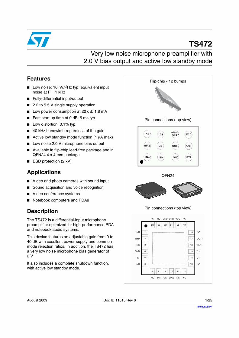
August 2009 Doc ID 11015 Rev 6 1/25
25
TS472Very low noise microphone preamplifier with
2.0 V bias output and active low standby mode
Features■ Low noise: 10 nV/√Hz typ. equivalent input
noise at F = 1 kHz
■ Fully-differential input/output
■ 2.2 to 5.5 V single supply operation
■ Low power consumption at 20 dB: 1.8 mA
■ Fast start up time at 0 dB: 5 ms typ.
■ Low distortion: 0.1% typ.
■ 40 kHz bandwidth regardless of the gain
■ Active low standby mode function (1 μA max)
■ Low noise 2.0 V microphone bias output
■ Available in flip-chip lead-free package and in QFN24 4 x 4 mm package
■ ESD protection (2 kV)
Applications■ Video and photo cameras with sound input
■ Sound acquisition and voice recognition
■ Video conference systems
■ Notebook computers and PDAs
DescriptionThe TS472 is a differential-input microphone preamplifier optimized for high-performance PDA and notebook audio systems.
This device features an adjustable gain from 0 to 40 dB with excellent power-supply and common-mode rejection ratios. In addition, the TS472 has a very low noise microphone bias generator of 2 V.
It also includes a complete shutdown function, with active low standby mode.
Flip-chip - 12 bumps
Pin connections (top view)
QFN24
Pin connections (top view)
1
2
3
4
5
6
7
13
14
15
16
17
18
192021222324
NC
BYP
NC
NC NC NC
NC
NC
NCNCNC
GND
IN-
8 9 10 11 12
NC
IN+ GS BIAS
C1
C2
OUT-
OUT+
GND STBY VCC
www.st.com
Contents TS472
2/25 Doc ID 11015 Rev 6
Contents
1 Typical application schematic . . . . . . . . . . . . . . . . . . . . . . . . . . . . . . . . . 3
2 Absolute maximum ratings . . . . . . . . . . . . . . . . . . . . . . . . . . . . . . . . . . . 5
3 Electrical characteristics . . . . . . . . . . . . . . . . . . . . . . . . . . . . . . . . . . . . . 6
4 Application information . . . . . . . . . . . . . . . . . . . . . . . . . . . . . . . . . . . . . 13
4.1 Differential configuration principle . . . . . . . . . . . . . . . . . . . . . . . . . . . . . . 13
4.2 Higher cut-off frequency . . . . . . . . . . . . . . . . . . . . . . . . . . . . . . . . . . . . . . 13
4.3 Lower cut-off frequency . . . . . . . . . . . . . . . . . . . . . . . . . . . . . . . . . . . . . . 14
4.4 Low-noise microphone bias source . . . . . . . . . . . . . . . . . . . . . . . . . . . . . 14
4.5 Gain settings . . . . . . . . . . . . . . . . . . . . . . . . . . . . . . . . . . . . . . . . . . . . . . 15
4.6 Wake-up time . . . . . . . . . . . . . . . . . . . . . . . . . . . . . . . . . . . . . . . . . . . . . . 16
4.7 Standby mode . . . . . . . . . . . . . . . . . . . . . . . . . . . . . . . . . . . . . . . . . . . . . 17
4.8 Layout considerations . . . . . . . . . . . . . . . . . . . . . . . . . . . . . . . . . . . . . . . . 17
4.9 Single-ended input configuration . . . . . . . . . . . . . . . . . . . . . . . . . . . . . . . 17
4.10 Demonstration board . . . . . . . . . . . . . . . . . . . . . . . . . . . . . . . . . . . . . . . . 18
5 Package information . . . . . . . . . . . . . . . . . . . . . . . . . . . . . . . . . . . . . . . . 19
5.1 Flip-chip package information . . . . . . . . . . . . . . . . . . . . . . . . . . . . . . . . . 19
5.2 QFN24 package information . . . . . . . . . . . . . . . . . . . . . . . . . . . . . . . . . . 21
6 Ordering information . . . . . . . . . . . . . . . . . . . . . . . . . . . . . . . . . . . . . . . 23
7 Revision history . . . . . . . . . . . . . . . . . . . . . . . . . . . . . . . . . . . . . . . . . . . 24
TS472 Typical application schematic
Doc ID 11015 Rev 6 3/25
1 Typical application schematic
Figure 1 shows a typical application schematic for the TS472.
Figure 1. Application schematic (flip-chip)
Table 1. Description of external components
Components Functional description
Cin+, Cin-Input coupling capacitors that block the DC voltage at the amplifier input terminal.
Cout+, Cout-
Output coupling capacitors that block the DC voltage coming from the amplifier output terminal (pins C2 and D2) and determine the lower cut-off frequency (see Section 4.3: Lower cut-off frequency).
Rout+, Rout-
Output load resistors used to charge the output coupling capacitors Cout. These output resistors can be represented by an input impedance of a following stage.
Rpos, Rneg Polarizing resistors for biasing of a microphone.
Cs Supply bypass capacitor that provides power supply filtering.
Cb Bypass pin capacitor that provides half-supply filtering.
C1, C2 Low pass filter capacitors allowing to cut the high frequency.
C3 Bias output filtering capacitor.
VCC
Electret Mic
Rpos
Rneg
Standby Control
Positive Output
Negative Output
1uFCb
1uFCs
1uFC3
C1
C2
Cin+
Cin-
+
Cout+
Cout-
Rout+
Rout-
Bias
ST
DB
Y
IN-
IN+
GC
1
C2
OUT+
OUT-
GAIN
BYPASSBIAS
GN
D
Vcc
SELECT
2.0V
U1 TS472_FC
Optional
Typical application schematic TS472
4/25 Doc ID 11015 Rev 6
Table 2. Pin descriptions
Pin nameFlip-chip
designatorQFN
designatorPin description
IN+ A1 8 Positive differential input
IN- B1 5 Negative differential input
BIAS A2 10 2 V bias output
GND C1 4, 22 Ground
STBY C3 21 Standby
BYP D1 2 Bypass
GS B2 9 Gain select
OUT- D2 16 Negative differential output
OUT+ C2 17 Positive differential output
C1 A3 14 Low-pass filter capacitor
C2 B3 15 Low-pass filter capacitor
Vcc D3 20 Power supply
NC ---3, 6, 7, 11, 12, 13, 18, 19, 23, 24
Not connected, floating pins
TS472 Absolute maximum ratings
Doc ID 11015 Rev 6 5/25
2 Absolute maximum ratings
Table 3. Absolute maximum ratings
Symbol Parameter Value Unit
VCC Supply voltage (1)
1. All voltage values are measured with respect to the ground pin.
6 V
Vi Input voltage -0.3 to VCC+0.3 V
Toper Operating free air temperature range -40 to + 85 °C
Tstg Storage temperature -65 to +150 °C
Tj Maximum junction temperature 150 °C
Rthja
Thermal resistance junction to ambient:
Flip-chipQFN24
180
110°C/W
ESD Human body model 2 kV
ESD Machine model 200 V
Lead temperature (soldering, 10sec) 250 °C
Table 4. Operating conditions
Symbol Parameter Value Unit
VCC Supply voltage 2.2 to 5.5 V
ATypical differential gain (GS connected to 4.7 kΩ or bias) 20 dB
VSTBY
Standby voltage input:
Device ONDevice OFF
1.5 ≤ VSTBY ≤ VCCGND ≤ VSTBY ≤ 0.4
V
Top Operational free air temperature range -40 to +85 °C
Rthja
Thermal resistance junction to ambient:Flip-chipQFN24
15060
°C/W
Electrical characteristics TS472
6/25 Doc ID 11015 Rev 6
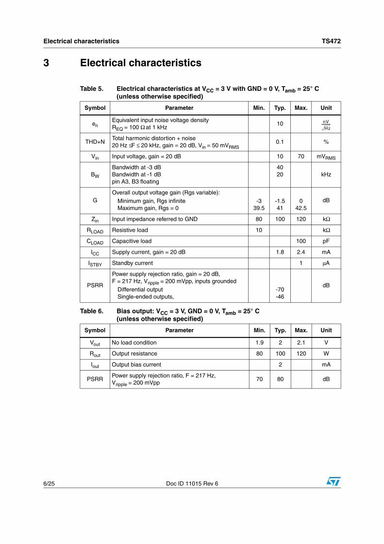
3 Electrical characteristics
Table 5. Electrical characteristics at VCC = 3 V with GND = 0 V, Tamb = 25° C (unless otherwise specified)
Symbol Parameter Min. Typ. Max. Unit
enEquivalent input noise voltage densityREQ = 100 Ω at 1 kHz
10
THD+NTotal harmonic distortion + noise20 Hz ≤F ≤ 20 kHz, gain = 20 dB, Vin = 50 mVRMS
0.1 %
Vin Input voltage, gain = 20 dB 10 70 mVRMS
BW
Bandwidth at -3 dBBandwidth at -1 dBpin A3, B3 floating
4020 kHz
GOverall output voltage gain (Rgs variable):
Minimum gain, Rgs infiniteMaximum gain, Rgs = 0
-339.5
-1.541
042.5
dB
Zin Input impedance referred to GND 80 100 120 kΩ
RLOAD Resistive load 10 kΩ
CLOAD Capacitive load 100 pF
ICC Supply current, gain = 20 dB 1.8 2.4 mA
ISTBY Standby current 1 μA
PSRR
Power supply rejection ratio, gain = 20 dB, F = 217 Hz, Vripple = 200 mVpp, inputs grounded
Differential outputSingle-ended outputs,
-70-46
dB
Table 6. Bias output: VCC = 3 V, GND = 0 V, Tamb = 25° C (unless otherwise specified)
Symbol Parameter Min. Typ. Max. Unit
Vout No load condition 1.9 2 2.1 V
Rout Output resistance 80 100 120 W
Iout Output bias current 2 mA
PSRRPower supply rejection ratio, F = 217 Hz, Vripple = 200 mVpp
70 80 dB
nV
Hz------------
TS472 Electrical characteristics
Doc ID 11015 Rev 6 7/25
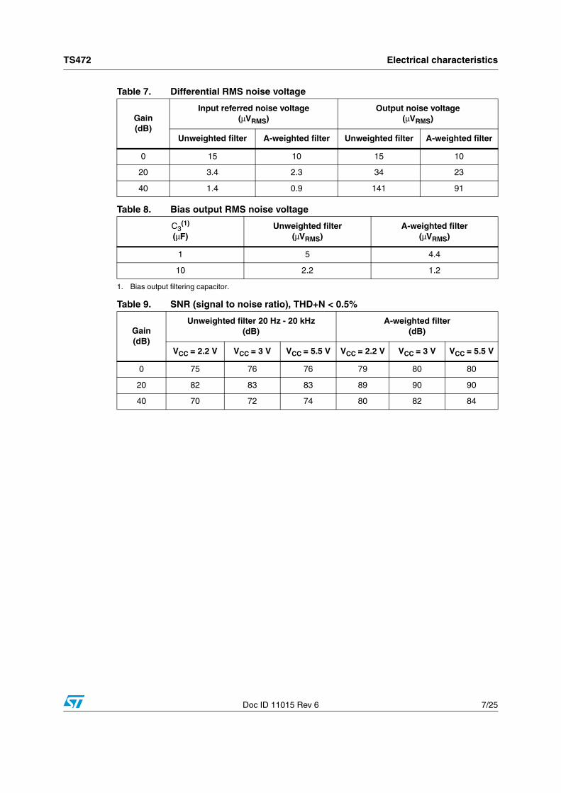
Table 7. Differential RMS noise voltage
Gain (dB)
Input referred noise voltage(μVRMS)
Output noise voltage(μVRMS)
Unweighted filter A-weighted filter Unweighted filter A-weighted filter
0 15 10 15 10
20 3.4 2.3 34 23
40 1.4 0.9 141 91
Table 8. Bias output RMS noise voltage
C3(1)
(μF)
1. Bias output filtering capacitor.
Unweighted filter(μVRMS)
A-weighted filter(μVRMS)
1 5 4.4
10 2.2 1.2
Table 9. SNR (signal to noise ratio), THD+N < 0.5%
Gain (dB)
Unweighted filter 20 Hz - 20 kHz(dB)
A-weighted filter(dB)
VCC = 2.2 V VCC = 3 V VCC = 5.5 V VCC = 2.2 V VCC = 3 V VCC = 5.5 V
0 75 76 76 79 80 80
20 82 83 83 89 90 90
40 70 72 74 80 82 84
Electrical characteristics TS472
8/25 Doc ID 11015 Rev 6
Figure 2. Current consumption vs. power supply voltage
Figure 3. Current consumption vs. power supply voltage
0 1 2 3 4 5 60.0
0.5
1.0
1.5
2.0
2.5
3.0
Tamb=85°C
Tamb=25°C
Tamb=-40°C
No LoadsGS floating
Cur
rent
Con
sum
ptio
n (m
A)
Power Supply Voltage (V) 0 1 2 3 4 5 6
0.0
0.5
1.0
1.5
2.0
2.5
3.0
Tamb=85°C
Tamb=25°C
Tamb=-40°C
No LoadsGS grounded
Cur
rent
Con
sum
ptio
n (m
A)
Power Supply Voltage (V)
Figure 4. Current consumption vs. standby voltage
Figure 5. Current consumption vs. standby voltage
0 1 2 3 4 50.0
0.5
1.0
1.5
2.0
2.5
Vcc=5VVcc=3V
No LoadsGS floatingTamb = 25°C
Cur
rent
Con
sum
ptio
n (m
A)
Standby Voltage (V) 0 1 2 3 4 5
0.0
0.5
1.0
1.5
2.0
2.5
Vcc=5VVcc=3V
No LoadsGS groundedTamb = 25°C
Cur
rent
Con
sum
ptio
n (m
A)
Standby Voltage (V)
Figure 6. Standby threshold voltage vs. power supply voltage
Figure 7. Frequency response
3 4 50.0
0.2
0.4
0.6
0.8
1.0
No LoadsTamb = 25°C
Sta
nd
by
Tre
sho
ld V
olt
age
(V)
Power Supply Voltage (V) 2.2 5.5 10 100 1000 10000 100000
-20
-10
0
10
20
30
C1,C2=220pF
C1,C2=100pF
Cin,Cout=10nF
Cin,Cout=100nF
no C1,C2
Cb=1μF, TAMB
=25°C, Gain=20dB, Rout=100kΩ
PS
RR
(d
B)
Frequency (Hz)
TS472 Electrical characteristics
Doc ID 11015 Rev 6 9/25
Figure 8. Bias output voltage vs. bias output current
Figure 9. Bias output voltage vs. power supply voltage
0 1 2 3 41.4
1.6
1.8
2.0
2.2
Tamb=85°C
Tamb=25°C
Bia
s O
utpu
t Vol
tage
(V)
Bias Output Current (mA)
Tamb=-40°C
Vcc=2.5-6V
3 4 51.4
1.6
1.8
2.0
2.2
Ibias=4mA
Ibias=2mA
Tamb=25°CIbias=0mA
Bia
s O
utp
ut
Vo
ltag
e (V
)
Power Supply Voltage (V) 2.2 5.5
Figure 10. Bias PSRR vs. frequency Figure 11. Bias PSRR vs. frequency
100 1000 10000-100
-80
-60
-40
-20
0Vripple=200mVppVcc=3VCb=1μFTamb =25°C
PS
RR
(d
B)
Frequency (Hz)
50 20k
Bias floating or 1kΩ to GND
100 1000 10000-100
-80
-60
-40
-20
0
Bias = 1kΩ to GND
Vripple=200mVppVcc=5VCb=1μFTamb=25°C
PS
RR
(d
B)
Frequency (Hz)
50 20k
Bias floating
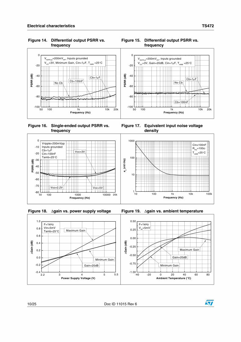
Figure 12. Differential output PSRR vs. frequency
Figure 13. Differential output PSRR vs. frequency
100 1000 10000-80
-70
-60
-50
-40
-30
-20
-10
0
GS=biasGS grounded
Vripple=200mVppInputs groundedVcc=3VCb=1μFCin=100nFTamb=25°C
GS floatingPS
RR
(d
B)
Frequency (Hz)50 20k 100 1000 10000
-80
-70
-60
-50
-40
-30
-20
-10
0
GS=biasGS grounded
Vripple=200mVppInputs groundedVcc=5VCb=1μFCin=100nFTamb=25°C
GS floating
PS
RR
(d
B)
Frequency (Hz)50 20k
Electrical characteristics TS472
10/25 Doc ID 11015 Rev 6
Figure 14. Differential output PSRR vs. frequency
Figure 15. Differential output PSRR vs. frequency
100 1k 10k-100
-80
-60
-40
-20
0V
RIPPLE=200mV
PP, Inputs grounded
VCC
=3V, Minimum Gain, Cin=1μF, TAMB
=25°C
Cb=1μF
No CbCb=100nF
PS
RR
(d
B)
Frequency (Hz)50 20k 100 1k 10k
-100
-80
-60
-40
-20
0V
RIPPLE=200mV
PP, Inputs grounded
VCC
=3V, Gain=20dB, Cin=1μF, TAMB
=25°C
Cb=1μFNo Cb
Cb=100nF
PS
RR
(d
B)
Frequency (Hz)50 20k
Figure 16. Single-ended output PSRR vs. frequency
Figure 17. Equivalent input noise voltage density
100 1000 10000-80
-70
-60
-50
-40
-30
-20
-10
0
Vcc=5VVcc=2.2V
Vcc=3V
Vripple=200mVppInputs groundedCb=1μFCin=100nFTamb=25°C
PS
RR
(d
B)
Frequency (Hz)50 20k 10 100 1k 10k 100k
1
10
100
1000
Cin=100nFR
EQ=100Ω
TAMB
=25°C
e n (n
V/√
Hz)
Frequency (Hz)
Figure 18. Δgain vs. power supply voltage Figure 19. Δgain vs. ambient temperature
3 4 5-0.4
-0.2
0.0
0.2
0.4
0.6
0.8
1.0
Maximum Gain
Gain=20dB
F=1kHzVin=5mVTamb=25°C
Minimum Gain
ΔG
ain
(d
B)
Power Supply Voltage (V) 2.2 5.5 -40 -20 0 20 40 60 80
-1.00
-0.75
-0.50
-0.25
0.00
0.25
0.50
Maximum Gain
F=1kHzV
IN=5mV
Gain=20dB
Minimum Gain
ΔG
ain
(d
B)
Ambient Temperature (°C)
TS472 Electrical characteristics
Doc ID 11015 Rev 6 11/25
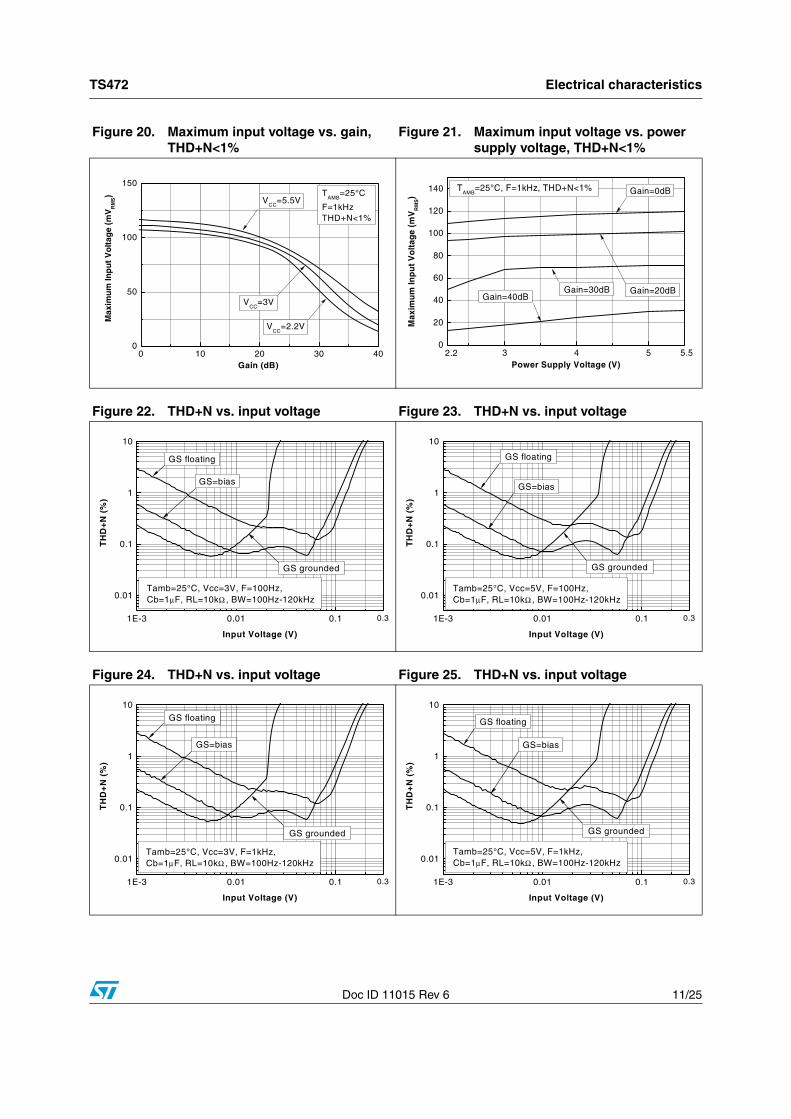
Figure 20. Maximum input voltage vs. gain, THD+N<1%
Figure 21. Maximum input voltage vs. power supply voltage, THD+N<1%
0 10 20 30 400
50
100
150
VCC
=2.2V
TAMB
=25°C
F=1kHzTHD+N<1%
Max
imu
m In
pu
t V
olt
age
(mV
RM
S)
Gain (dB)
VCC
=5.5V
VCC
=3V
3 4 50
20
40
60
80
100
120
140
Gain=20dB
Gain=0dBTAMB
=25°C, F=1kHz, THD+N<1%
Max
imu
m In
pu
t V
olt
age
(mV
RM
S)
Power Supply Voltage (V)
Gain=30dBGain=40dB
2.2 5.5
Figure 22. THD+N vs. input voltage Figure 23. THD+N vs. input voltage
1E-3 0.01 0.1
0.01
0.1
1
10
GS=bias
GS grounded
Tamb=25°C, Vcc=3V, F=100Hz,Cb=1μF, RL=10kΩ , BW=100Hz-120kHz
TH
D+
N (
%)
Input Voltage (V)
0.3
GS floating
1E-3 0.01 0.1
0.01
0.1
1
10
GS grounded
GS floating
GS=bias
Tamb=25°C, Vcc=5V, F=100Hz,Cb=1μF, RL=10kΩ , BW=100Hz-120kHz
TH
D+
N (
%)
Input Voltage (V)
0.3
Figure 24. THD+N vs. input voltage Figure 25. THD+N vs. input voltage
1E-3 0.01 0.1
0.01
0.1
1
10
GS grounded
GS=bias
Tamb=25°C, Vcc=3V, F=1kHz, Cb=1μF, RL=10kΩ , BW=100Hz-120kHz
TH
D+
N (
%)
Input Voltage (V)
0.3
GS floating
1E-3 0.01 0.1
0.01
0.1
1
10
GS grounded
GS=bias
GS floating
Tamb=25°C, Vcc=5V, F=1kHz,Cb=1μF, RL=10kΩ , BW=100Hz-120kHz
TH
D+
N (
%)
Input Voltage (V)
0.3
Electrical characteristics TS472
12/25 Doc ID 11015 Rev 6
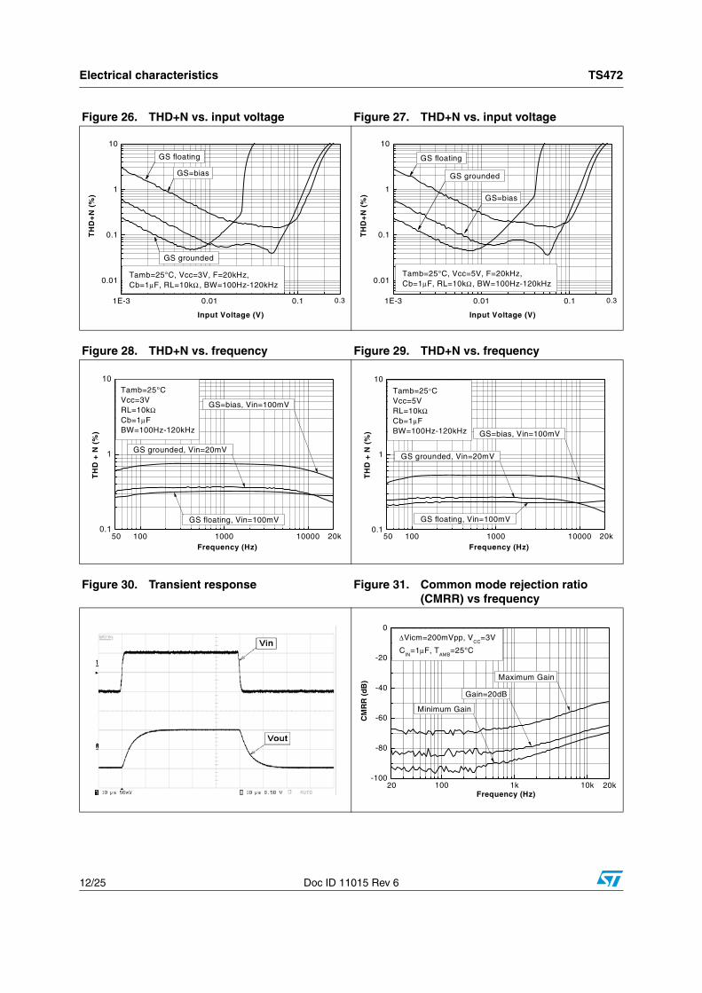
Figure 26. THD+N vs. input voltage Figure 27. THD+N vs. input voltage
1E-3 0.01 0.1
0.01
0.1
1
10
GS grounded
GS=bias
Tamb=25°C, Vcc=3V, F=20kHz,Cb=1μF, RL=10kΩ , BW=100Hz-120kHz
TH
D+
N (
%)
Input Voltage (V)
0.3
GS floating
1E-3 0.01 0.1
0.01
0.1
1
10
GS floating
GS=bias
GS grounded
Tamb=25°C, Vcc=5V, F=20kHz,Cb=1μF, RL=10kΩ , BW=100Hz-120kHz
TH
D+
N (
%)
Input Voltage (V)
0.3
Figure 28. THD+N vs. frequency Figure 29. THD+N vs. frequency
100 1000 100000.1
1
10
GS=bias, Vin=100mV
GS floating, Vin=100mV
GS grounded, Vin=20mV
Tamb=25°CVcc=3VRL=10kΩCb=1μFBW=100Hz-120kHz
20k50
TH
D +
N (
%)
Frequency (Hz)100 1000 10000
0.1
1
10
GS=bias, Vin=100mV
GS floating, Vin=100mV
GS grounded, Vin=20mV
Tamb=25°CVcc=5VRL=10kΩCb=1μFBW=100Hz-120kHz
20k50
TH
D +
N (
%)
Frequency (Hz)
Figure 30. Transient response Figure 31. Common mode rejection ratio (CMRR) vs frequency
100 1k 10k-100
-80
-60
-40
-20
0ΔVicm=200mVpp, V
CC=3V
CIN
=1μF, TAMB
=25°C
Gain=20dB
Maximum Gain
Minimum Gain
CM
RR
(d
B)
Frequency (Hz)20 20k
TS472 Application information
Doc ID 11015 Rev 6 13/25
4 Application information
4.1 Differential configuration principleThe TS472 is a fully-differential input/output microphone preamplifier. The TS472 also includes a common-mode feedback loop that controls the output bias value to average it at VCC/2. This allows the device to always have a maximum output voltage swing, and by consequence, maximize the input dynamic voltage range.
The advantages of a fully-differential amplifier are:
● Very high PSRR (power supply rejection ratio).
● High common mode noise rejection.
● In theory, the filtering of the internal bias by an external bypass capacitor is not necessary. However, to reach maximum performance in all tolerance situations, it is better to keep this option.
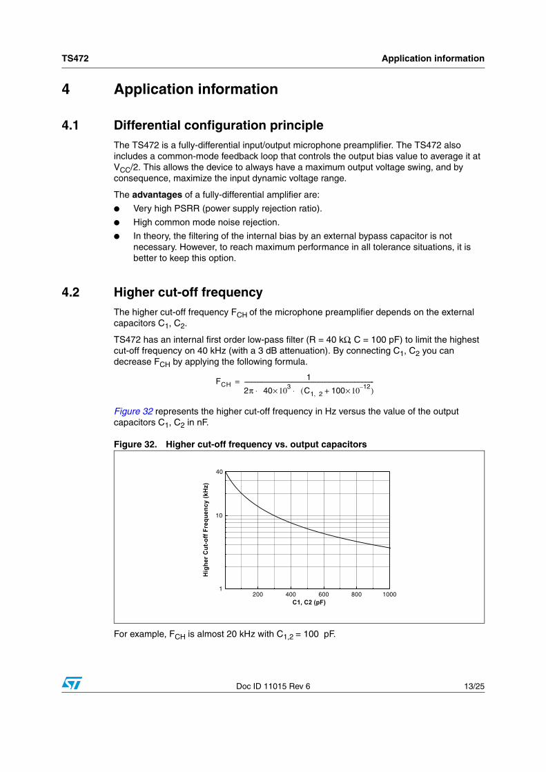
4.2 Higher cut-off frequencyThe higher cut-off frequency FCH of the microphone preamplifier depends on the external capacitors C1, C2.
TS472 has an internal first order low-pass filter (R = 40 kΩ, C = 100 pF) to limit the highest cut-off frequency on 40 kHz (with a 3 dB attenuation). By connecting C1, C2 you can decrease FCH by applying the following formula.
Figure 32 represents the higher cut-off frequency in Hz versus the value of the output capacitors C1, C2 in nF.
Figure 32. Higher cut-off frequency vs. output capacitors
For example, FCH is almost 20 kHz with C1,2 = 100 pF.
FCH1
2π 40 3× 10 C1 2, 100 12–× 10+( )⋅ ⋅----------------------------------------------------------------------------------------------=
200 400 600 800 10001
10
Hig
her C
ut-o
ff Fr
eque
ncy
(kH
z)
C1, C2 (pF)
40
Application information TS472
14/25 Doc ID 11015 Rev 6
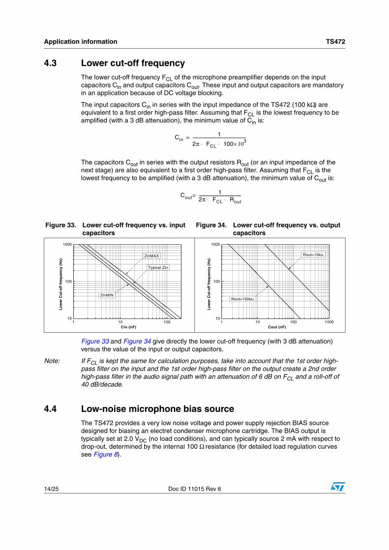
4.3 Lower cut-off frequencyThe lower cut-off frequency FCL of the microphone preamplifier depends on the input capacitors Cin and output capacitors Cout. These input and output capacitors are mandatory in an application because of DC voltage blocking.
The input capacitors Cin in series with the input impedance of the TS472 (100 kΩ) are equivalent to a first order high-pass filter. Assuming that FCL is the lowest frequency to be amplified (with a 3 dB attenuation), the minimum value of Cin is:
The capacitors Cout in series with the output resistors Rout (or an input impedance of the next stage) are also equivalent to a first order high-pass filter. Assuming that FCL is the lowest frequency to be amplified (with a 3 dB attenuation), the minimum value of Cout is:
Figure 33 and Figure 34 give directly the lower cut-off frequency (with 3 dB attenuation) versus the value of the input or output capacitors.
Note: If FCL is kept the same for calculation purposes, take into account that the 1st order high-pass filter on the input and the 1st order high-pass filter on the output create a 2nd order high-pass filter in the audio signal path with an attenuation of 6 dB on FCL and a roll-off of 40 dB/decade.
4.4 Low-noise microphone bias sourceThe TS472 provides a very low noise voltage and power supply rejection BIAS source designed for biasing an electret condenser microphone cartridge. The BIAS output is typically set at 2.0 VDC (no load conditions), and can typically source 2 mA with respect to drop-out, determined by the internal 100 Ω resistance (for detailed load regulation curves see Figure 8).
Cin1
2π FCL 100 3× 10⋅ ⋅------------------------------------------------------=
Cout1
2π FCL Rout⋅ ⋅-------------------------------------------=
Figure 33. Lower cut-off frequency vs. input capacitors
Figure 34. Lower cut-off frequency vs. output capacitors
1 10 10010
100
1000
Typical Zin
ZinMAX
Lo
wer
Cu
t-o
ff f
req
uen
cy (
Hz)
Cin (nF)
ZinMIN
1 10 100 100010
100
1000
Rout=10kΩ
Lo
wer
Cu
t-o
ff f
req
uen
cy (
Hz)
Cout (nF)
Rout=100kΩ
TS472 Application information
Doc ID 11015 Rev 6 15/25
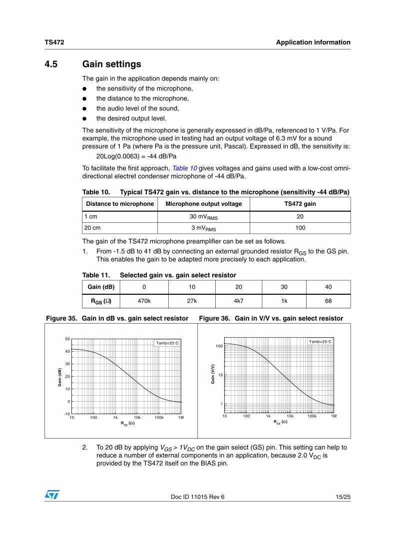
4.5 Gain settingsThe gain in the application depends mainly on:
● the sensitivity of the microphone,
● the distance to the microphone,
● the audio level of the sound,
● the desired output level.
The sensitivity of the microphone is generally expressed in dB/Pa, referenced to 1 V/Pa. For example, the microphone used in testing had an output voltage of 6.3 mV for a sound pressure of 1 Pa (where Pa is the pressure unit, Pascal). Expressed in dB, the sensitivity is:
20Log(0.0063) = -44 dB/Pa
To facilitate the first approach, Table 10 gives voltages and gains used with a low-cost omni-directional electret condenser microphone of -44 dB/Pa.
The gain of the TS472 microphone preamplifier can be set as follows.
1. From -1.5 dB to 41 dB by connecting an external grounded resistor RGS to the GS pin. This enables the gain to be adapted more precisely to each application.
2. To 20 dB by applying VGS > 1VDC on the gain select (GS) pin. This setting can help to reduce a number of external components in an application, because 2.0 VDC is provided by the TS472 itself on the BIAS pin.
Table 10. Typical TS472 gain vs. distance to the microphone (sensitivity -44 dB/Pa)
Distance to microphone Microphone output voltage TS472 gain
1 cm 30 mVRMS 20
20 cm 3 mVRMS 100
Table 11. Selected gain vs. gain select resistor
Gain (dB) 0 10 20 30 40
RGS (Ω) 470k 27k 4k7 1k 68
Figure 35. Gain in dB vs. gain select resistor Figure 36. Gain in V/V vs. gain select resistor
10 100 1k 10k 100k 1M-10
0
10
20
30
40
50Tamb=25°C
Gai
n (
dB
)
RGS
(Ω)10 100 1k 10k 100k 1M
1
10
100
Gai
n (
V/V
)
Tamb=25°C
RGS
(Ω)
Application information TS472
16/25 Doc ID 11015 Rev 6
Figure 37 gives other values of the gain vs. voltage applied on the GS pin.
Figure 37. Gain vs. gain select voltage
Note: In the case of a single-ended output configuration (either positive or negative output is used for the following signal processing) the overall gain is half. One must also take into account that all advantages of the differential configuration principles are lost (see the difference in PSRR in Table 5).
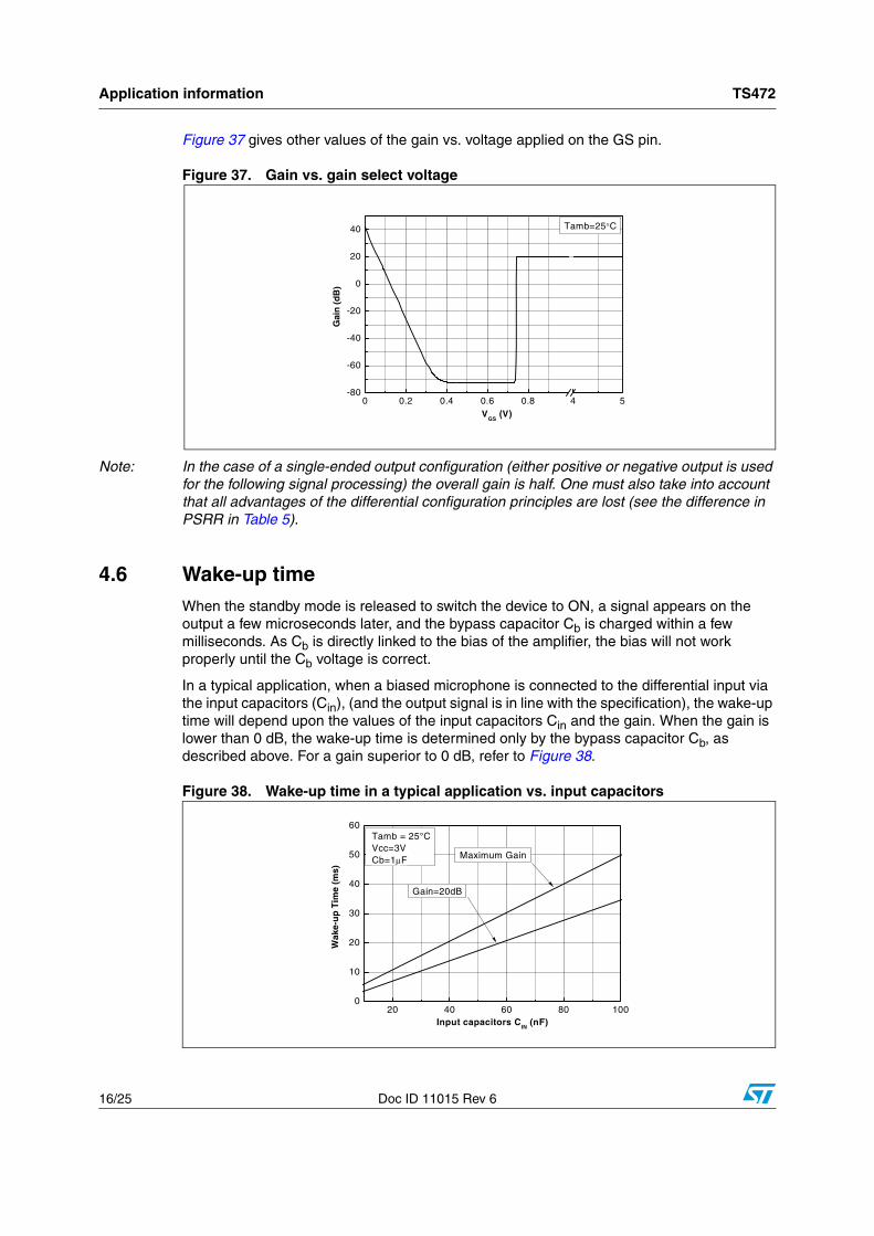
4.6 Wake-up timeWhen the standby mode is released to switch the device to ON, a signal appears on the output a few microseconds later, and the bypass capacitor Cb is charged within a few milliseconds. As Cb is directly linked to the bias of the amplifier, the bias will not work properly until the Cb voltage is correct.
In a typical application, when a biased microphone is connected to the differential input via the input capacitors (Cin), (and the output signal is in line with the specification), the wake-up time will depend upon the values of the input capacitors Cin and the gain. When the gain is lower than 0 dB, the wake-up time is determined only by the bypass capacitor Cb, as described above. For a gain superior to 0 dB, refer to Figure 38.
Figure 38. Wake-up time in a typical application vs. input capacitors
0 0.2 0.4 0.6 0.8 4 5-80
-60
-40
-20
0
20
40 Tamb=25°C
Gai
n (
dB
)
VGS
(V)
20 40 60 80 1000
10
20
30
40
50
60
Gain=20dB
Tamb = 25°CVcc=3VCb=1μF
Wak
e-u
p T
ime
(ms)
Input capacitors CIN
(nF)
Maximum Gain
TS472 Application information
Doc ID 11015 Rev 6 17/25
4.7 Standby modeWhen the standby command is set, it takes a few microseconds to set the output stages (differential outputs and 2.0 V bias output) to high impedance and the internal circuitry to shutdown mode.
4.8 Layout considerationsThe TS472 has sensitive pins to connect C1, C2 and Rgs. To obtain high power supply rejection and low noise performance, it is mandatory that the layout track to these components be as short as possible.
Decoupling capacitors on VCC and bypass pin are needed to eliminate power supply drops. In addition, the capacitor location for the dedicated pin should be as close to the device as possible.
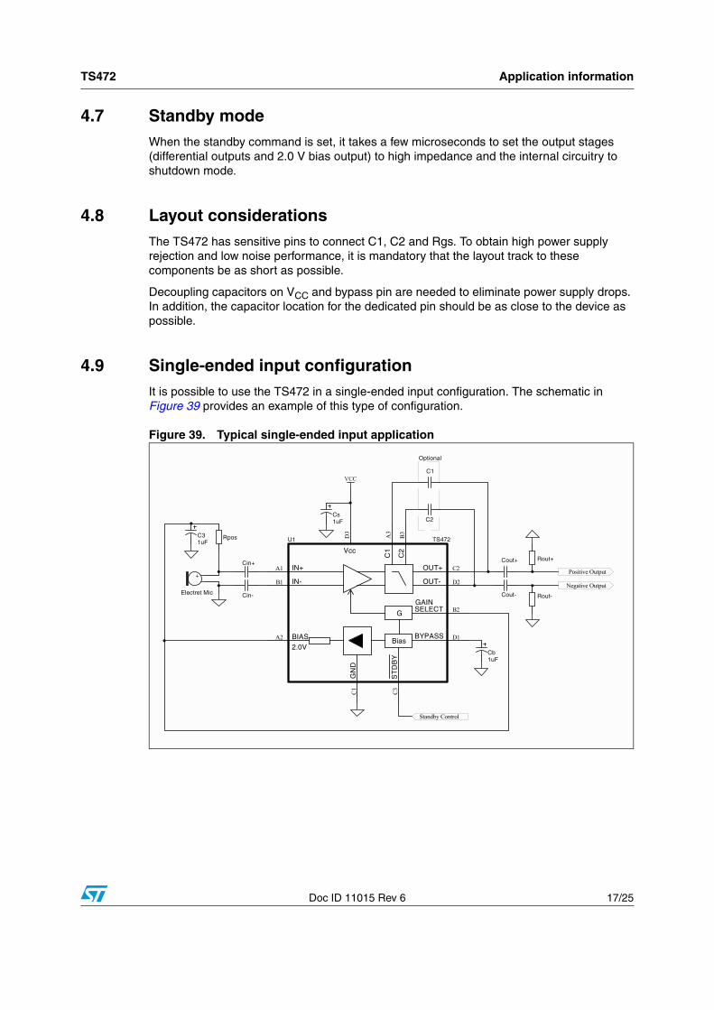
4.9 Single-ended input configurationIt is possible to use the TS472 in a single-ended input configuration. The schematic in Figure 39 provides an example of this type of configuration.
Figure 39. Typical single-ended input application
VCC
Electret Mic
Rpos
Standby Control
Positive Output
Negative Output
1uFCb
1uFCs
1uFC3
C1
C2
Cin+
Cin-
+
Cout+
Cout-
Rout+
Rout-
Bias
ST
DB
Y
IN-
IN+
G
C1
C2
OUT+
OUT-
GAIN
BYPASSBIAS
GN
D
Vcc
SELECT
D3
A3
B3
C2
D2
B2
D1
C3
C1
A2
B1
A1
2.0V
U1 TS472
Optional
Application information TS472
18/25 Doc ID 11015 Rev 6
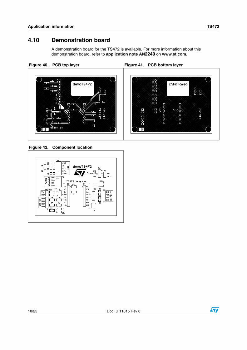
4.10 Demonstration boardA demonstration board for the TS472 is available. For more information about this demonstration board, refer to application note AN2240 on www.st.com.
Figure 40. PCB top layer Figure 41. PCB bottom layer
Figure 42. Component location
TS472 Package information
Doc ID 11015 Rev 6 19/25
5 Package information
In order to meet environmental requirements, ST offers these devices in different grades of ECOPACK® packages, depending on their level of environmental compliance. ECOPACK® specifications, grade definitions and product status are available at: www.st.com. ECOPACK® is an ST trademark.
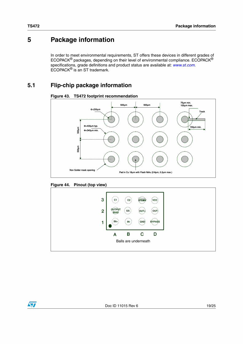
5.1 Flip-chip package information
Figure 43. TS472 footprint recommendation
Figure 44. Pinout (top view)
Pad in Cu 18μm with Flash NiAu (2-6μm, 0.2μm max.)
150μm min.
500μm
500μ
m
500μm
500μ
m
Φ=250μm
Φ=400μm typ.
75µm min.100μm max.
Track
Non Solder mask opening
Φ=340μm min.
Pad in Cu 18μm with Flash NiAu (2-6μm, 0.2μm max.)
150μm min.
500μm
500μ
m
500μm
500μ
m
Φ=250μm
Φ=400μm typ.
75µm min.100μm max.
Track
Non Solder mask opening
Φ=340μm min.
A CB
1
2
3
D
IN+ IN- GND
OUT+
C2C1
OUTPUTBIAS
GS
VCC
OUT-
STDBY
BYPASS
A CB
1
2
3
D
IN+ IN- GND
OUT+
C2C1
OUTPUTBIAS
GS
VCC
OUT-
STDBYSTDBY
BYPASS
Balls are underneath
Package information TS472
20/25 Doc ID 11015 Rev 6
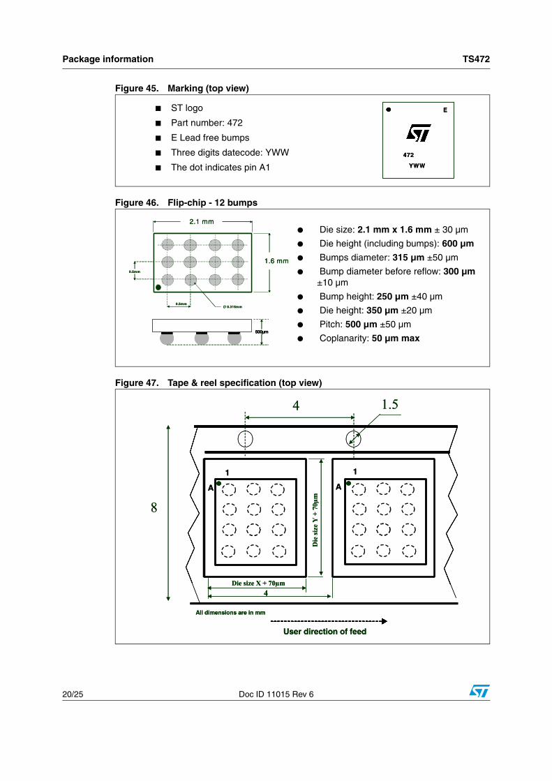
Figure 45. Marking (top view)
Figure 46. Flip-chip - 12 bumps
Figure 47. Tape & reel specification (top view)
472
YWW
E
472
YWW
E■ ST logo
■ Part number: 472
■ E Lead free bumps
■ Three digits datecode: YWW
■ The dot indicates pin A1
● Die size: 2.1 mm x 1.6 mm ± 30 µm
● Die height (including bumps): 600 µm
● Bumps diameter: 315 µm ±50 µm
● Bump diameter before reflow: 300 µm ±10 µm
● Bump height: 250 µm ±40 µm
● Die height: 350 µm ±20 µm
● Pitch: 500 µm ±50 µm
● Coplanarity: 50 µm max
2.1 mm
1.6 mm
0.5mm
0.5mm
∅ 0.315mm
2.1 mm
1.6 mm
0.5mm
0.5mm
∅ 0.315mm
600µm600µm
User direction of feed
8
Die size X + 70µm
Die
size
Y +
70µ
m
4 1.5
4
All dimensions are in mm
A
1
A
1
User direction of feed
8
Die size X + 70µm
Die
size
Y +
70µ
m
4 1.5
4
All dimensions are in mm
A
1
A
1
TS472 Package information
Doc ID 11015 Rev 6 21/25
5.2 QFN24 package information
Figure 48. QFN24 package mechanical drawing
A
SEATINGPLANE
0
A1
0.50 DIA.
D1
D
E1 E
Nd
2
3
1
Ne
3
2
b
1
e
L
P
Q
R
E2
D2
A2
Package information TS472
22/25 Doc ID 11015 Rev 6
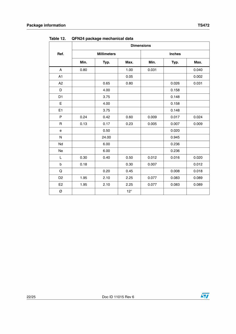
Table 12. QFN24 package mechanical data
Ref.
Dimensions
Millimeters Inches
Min. Typ. Max. Min. Typ. Max.
A 0.80 1.00 0.031 0.040
A1 0.05 0.002
A2 0.65 0.80 0.026 0.031
D 4.00 0.158
D1 3.75 0.148
E 4.00 0.158
E1 3.75 0.148
P 0.24 0.42 0.60 0.009 0.017 0.024
R 0.13 0.17 0.23 0.005 0.007 0.009
e 0.50 0.020
N 24.00 0.945
Nd 6.00 0.236
Ne 6.00 0.236
L 0.30 0.40 0.50 0.012 0.016 0.020
b 0.18 0.30 0.007 0.012
Q 0.20 0.45 0.008 0.018
D2 1.95 2.10 2.25 0.077 0.083 0.089
E2 1.95 2.10 2.25 0.077 0.083 0.089
Ø 12°
TS472 Ordering information
Doc ID 11015 Rev 6 23/25
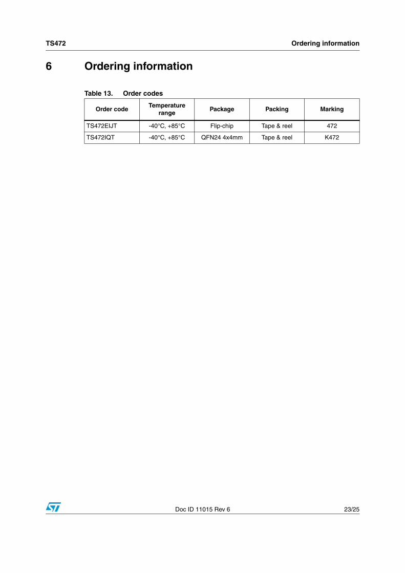
6 Ordering information
Table 13. Order codes
Order codeTemperature
rangePackage Packing Marking
TS472EIJT -40°C, +85°C Flip-chip Tape & reel 472
TS472IQT -40°C, +85°C QFN24 4x4mm Tape & reel K472
Revision history TS472
24/25 Doc ID 11015 Rev 6
7 Revision history
Table 14. Document revision history
Date Revision Changes
01-Jul-05 1 Initial release corresponding to product preview version.
01-Oct-05 2 First release of fully mature product datasheet.
01-Dec-05 3Added single-ended input operation in Section 4: Application information.
12-Sep-2006 4Added QFN package information. Updated curves, added new ones in Section 3: Electrical characteristics.
02-Mar-2009 5
Corrected error on C1 and C2 caps.
Added Table 2: Pin descriptions.
Updated QFN24 package information in Section 5.2.
25-Aug-2009 6 Corrected QFN package pinout on cover page.
TS472
Doc ID 11015 Rev 6 25/25
Please Read Carefully:
Information in this document is provided solely in connection with ST products. STMicroelectronics NV and its subsidiaries (“ST”) reserve theright to make changes, corrections, modifications or improvements, to this document, and the products and services described herein at anytime, without notice.
All ST products are sold pursuant to ST’s terms and conditions of sale.
Purchasers are solely responsible for the choice, selection and use of the ST products and services described herein, and ST assumes noliability whatsoever relating to the choice, selection or use of the ST products and services described herein.
No license, express or implied, by estoppel or otherwise, to any intellectual property rights is granted under this document. If any part of thisdocument refers to any third party products or services it shall not be deemed a license grant by ST for the use of such third party productsor services, or any intellectual property contained therein or considered as a warranty covering the use in any manner whatsoever of suchthird party products or services or any intellectual property contained therein.
UNLESS OTHERWISE SET FORTH IN ST’S TERMS AND CONDITIONS OF SALE ST DISCLAIMS ANY EXPRESS OR IMPLIEDWARRANTY WITH RESPECT TO THE USE AND/OR SALE OF ST PRODUCTS INCLUDING WITHOUT LIMITATION IMPLIEDWARRANTIES OF MERCHANTABILITY, FITNESS FOR A PARTICULAR PURPOSE (AND THEIR EQUIVALENTS UNDER THE LAWSOF ANY JURISDICTION), OR INFRINGEMENT OF ANY PATENT, COPYRIGHT OR OTHER INTELLECTUAL PROPERTY RIGHT.
UNLESS EXPRESSLY APPROVED IN WRITING BY AN AUTHORIZED ST REPRESENTATIVE, ST PRODUCTS ARE NOTRECOMMENDED, AUTHORIZED OR WARRANTED FOR USE IN MILITARY, AIR CRAFT, SPACE, LIFE SAVING, OR LIFE SUSTAININGAPPLICATIONS, NOR IN PRODUCTS OR SYSTEMS WHERE FAILURE OR MALFUNCTION MAY RESULT IN PERSONAL INJURY,DEATH, OR SEVERE PROPERTY OR ENVIRONMENTAL DAMAGE. ST PRODUCTS WHICH ARE NOT SPECIFIED AS "AUTOMOTIVEGRADE" MAY ONLY BE USED IN AUTOMOTIVE APPLICATIONS AT USER’S OWN RISK.
Resale of ST products with provisions different from the statements and/or technical features set forth in this document shall immediately voidany warranty granted by ST for the ST product or service described herein and shall not create or extend in any manner whatsoever, anyliability of ST.
ST and the ST logo are trademarks or registered trademarks of ST in various countries.
Information in this document supersedes and replaces all information previously supplied.
The ST logo is a registered trademark of STMicroelectronics. All other names are the property of their respective owners.
© 2009 STMicroelectronics - All rights reserved
STMicroelectronics group of companies
Australia - Belgium - Brazil - Canada - China - Czech Republic - Finland - France - Germany - Hong Kong - India - Israel - Italy - Japan - Malaysia - Malta - Morocco - Philippines - Singapore - Spain - Sweden - Switzerland - United Kingdom - United States of America
www.st.com


![Welcome []...tel 1.303.823.8100 fax 1.303.823.8101 info@gracedesign.com / grace design m201 owner’s manual 2 Welcome Thank you for purchasing the Grace Design m201 microphone preamplifier](https://img.pdfslide.net/doc/110x75/5e6d924dfd04733f763d568b/welcome-tel-13038238100-fax-13038238101-info-grace-design-m201.jpg)