Embed Size (px)
Citation preview

VHDL for Logic Synthesis

Overview
• Design Flow for Hardware Design
• VHDL coding for synthesis
• General guidelines for hardware designers
2
This lecture includes the content from:
Nitin Yogi, Modelling for Synthesis with VHDL, Auburn University
Actel HDL Coding Style Guide
and other sources

Digital design flow (ASIC; FPGA)
System Design Flow
Mixed-signal Wireless Comm Embedded Computing Architectures
MATLAB model - floating point
MATLAB model - fixed point
RTL coding (VHDL)
ASIC Logic Synthesis (Synopsys),
FPGA LS (Xilinx ISE)
ASIC Back-End (CADENCE SE),
FPGA P&R (Xilinx ISE)
ASIC DRC & LVS
(Cadence Assura, Polyteda)
High Level Synthesis
(CtoS, CatapultC,
HandelC)
HwSw Partitioning – based on
profiling
RTL coding (VHDL)
Software
flow
Verification flow
-based on system level
verification
-Assertions and formal
verification actively
used
-Smart testbenches
- FPGA verification
- Palladium verification
DfT flow
- BIST for memory and
logic
- Scan for logic
Electronic System Level (ESL) flow –System C – TLM, Verification, Profiling -VISTA
Reconfugurable
IP Cores –
Internal &
External
(SystemC,
MATLAB, VHDL)
Simulink flow
Palladium XP
3

VLSI Levels of Abstraction
Specification (what the chip does, inputs/outputs)
System Level Modeling major resources, connections
Register-Transfer logic blocks, FSMs, memory, connections
Circuit transistors, parasitics, connections
Layout mask layers, polygons
Logic gates, flip-flops, latches, connections
4

Activity Flow in Digital Design
5
Functional Design
RTL Design
Logic Design
Circuit Design
Physical Design
specifications
GDS description
Behavioural description and
verification
RTL description and
verification
Netlist synthesis and
simulation
Timing Closure
Power Analysis
Physical Analysis (DRC,
LVS, ERC)

ASIC Design flow IP Library
HDL RTL Designs
HDL Top Module Definition
Simulation
Result
OK?
Logic Synthesis
Simulation
Result
OK?
Layout Synthesis
Simulation
Result
OK?
Final Chip Layout
Test Benches
yes
IP
New
synthesis
yes
yes New layout
run
sufficient?
ye
s
no
no
no
no
yes
no
Applications
System Specification
6
6

Design Views and Abstraction Models
7
• Process of ASIC design starts with behavioral model, goes over
structural until physical model
BEHAVIOURAL STRUCTURAL
PHYSICAL
algorithms
Register transfers
Signals, expressions gates
registers
processors
MPSoC
transistors
cells
modules
chips

VHDL could be applied at multiple levels of abstraction
8
• For detailed view please visit “Entwurf Digitaler Systeme”
• VHDL can be used to model the circuit of very abstract behavioral
level
• This description can be refined to the RTL level
• Also it can be used for describing the structural netlist
After synthesis
Cell Delay
After layout
Cell Delay
Interconnect Delay

Synthesis Process and different coding Styles
• Synthesis converts RTL model to structural model
• As a result we get some sort of a netlist (VHDL, Verilog (most frequently), EDIF)
Behavioral (RTL) model architecture behav of mux is
begin
pr: process(A,B,C)
begin
if (S = '0') then
Y <= A;
else
Y <= B;
end if;
end process pr;
end;
Structural model architecture netlist of mux is
signal CI, D, E:std_logic
begin
g1: not port map (CI,C);
g2: and port map (D,A,CI);
g3: and port map (E,B,C);
g4: or port map (Y,D,E);
end; A
B
C Y
Synthesis
9

Why we should know the synthesis outcome while describing VHDL?
Behavioral model
architecture behav of cont is
begin
p1: process(A,B,C1, C2)
begin
if (C1 = ‘1') and (C2 = '1') then
Out1 <= A;
elsif (C2 = ‘1') then
Out2 <= B;
--else we do not care
end if;
end process p1;
end;
Synthesis
Expected result of synthesis
Obtained synthesized design!
10
A
C2
C1
Out1
MU
X B
A
C2
C1
Out1 MU
X B
D Out
Latch
EN

Why is suboptimal design dangerous?
11
• Additional hardware leads to overhead in the area -> additional cost
• Additional hardware means additional power consumption -> reduced battery time
• Suboptimal design have reduced performances -> longer critical path
• Unclarities in the design create potential bugs
• (Unintentional) use of latches may lead to problems in timing analysis and glitch generation
Why we should know the synthesis outcome while describing VHDL?
- Corrected Design
Behavioral model
architecture behav of cont is
begin
p1: process(A,B,C1, C2)
begin
if (C1 = ‘1') and (C2 = '1') then
Out1 <= A;
elsif (C2 = ‘1') then
Out2 <= B;
else
Out2<=‘B’;
end if;
end process p1;
end;
Synthesis
12
A
C2
C1
Out1
MU
X B
Rule of correctly written VHDL:
Always define the outputs for all IF cases

Typical Digital Circuits
• Combinational logic circuits
random logic
multiplexers
Decoders
• Arithmetic functions
• Sequential logic (registers)
synchronous & asynchronous inputs
• Shift registers
• Finite state machines
• Memory synthesis
• More advanced circuits (FIFOs, synchronizers, clock gates)
13

How VHDL Simulator works?
• VHDL blocks are simulated using event based simulator
• Assignments are concurrently executed
• Update for all assignments in particular timestamp is performed at the same time
• Following assignments (depending on the updates from the previous calculations) are updated with delta cycle delay
• Delta cycle delay is simulation quantum time which cannot be visualized, but enables effective execution of events.
• When all assignments are eventually resolved (after N delta cycles) the simulator can go to the next timing event in the simulation.
X<= Y+ Z; -- assignment executed after delta cycle
W<= X-Z; -- after updating the value of X, we will update the value of W as well, -- however with one delta cycle delay compared to the X update
Please be careful:
A<=B;
In this case signals A and B are not identical, and there is a delta delay in between

Variables and Signals
• Variables are used only within the process
Usually they are utilized for holding the immediate results of the
calculation (it is also difficult to visualize them in the simulation)
Variables are updated immediately (without delta cycle delay)
They enable sequential execution in the process
• Signals are always executed with delta delay cycle
Behavioral model
architecture behav of cont is
begin
p1: process(A,B,C1, C2)
variable Temp:std_logic:=‘0’; --initial value!
begin
if (C1 = ‘1') and (C2 = '1') then
temp := A;
elsif (C2 = ‘1') then
temp:= B;
else
temp:=‘B’;
end if;
Out1<=B;
end process p1;
end;
Behavioral model
architecture behav of ex1 is
begin
p1: process(clk)
variable Temp1,
Temp2:std_logic;
begin
if (clk = ‘1') and clk’event then
temp1 := A;
temp2 :=temp1;
Out1:=temp2;
end if;
end process p1;
end;
Behavioral model
architecture behav of ex2 is
begin
p1: process(clk)
variable Temp1,
Temp2:std_logic;
begin
if (clk = ‘1') and clk’event then
Out1:=temp2;
temp1 := A;
temp2 :=temp1;
-- order of operation matters!
end if;
end process p1;
end;

VHDL Coding Styles
• Behavioural
Behavioral model
architecture behav of cont is
begin
p1: process(A,B,C1, C2)
begin
if (C1 = ‘1') and (C2 =
'1') then
Out1 <= A;
else
Out2 <= B;
end if;
end process p1;
end;
• Structural
architecture netlist of cont is
signal CI, D, E:std_logic
begin
g1: not port map (CI,C);
g2: and port map (D,A,CI);
g3: and port map (E,B,C);
g4: or port map (Out1,D,E);
end;
• Dataflow
architecture dataflow of cont is
begin
Out1<=A when C1=‘1’ and
C2=‘1’ else B;
end;

Sensitivity list in Combinational Logic
Behavioral model
architecture behav of cont is
begin
p1: process(A,B, C2) – missing C1
begin
if (C1 = ‘1') and (C2 = '1') then
Out1 <= A;
else
Out2 <= B;
end if;
end process p1;
end;
17
• All signals affecting results of the combinational process need to be
in the sensitivity list
• Otherwise the simulation results will not be representative
• For synchronous circuits it is only required to have clock (and
asynchronous set/reset in the list
• Why is this so?

Multiplexer: Using “case” Statement
entity Mux4 is
port (in1: in std_logic_vector(3 downto 0);
s1: in std_logic_vector (1 downto 0);
m: out std_logic);
end Mux4;
architecture behav of Mux4 is
begin
process(s1, in1)
begin
case s1 is
when "00" => m <= i(0);
when "01" => m <= i(1);
when "10" => m <= i(2);
when others => m <= i(3); -- why this?
end case;
end process;
end behav;
18
MU
X
in1
S1
m

Multiplexer: dataflow implementation
entity Mux4 is
port (in1: in std_logic_vector(3 downto 0);
s1: in std_logic_vector (1 downto 0);
m: out std_logic);
end Mux4;
architecture behav of Mux4 is
begin
with s1 select
when "00" => m <= i(0);
when "01" => m <= i(1);
when "10" => m <= i(2);
when others => m <= i(3);
end behav;
This implementation is safer for unexperienced designers => no problems with sensitivity list and complete definition of cases
19
MU
X
in1
S1
m

Priority encoder
entity enc is
port (in1: in std_logic_vector(3 downto 0);
s1: in std_logic_vector (1 downto 0);
m: out std_logic);
end enc;
architecture behav of enc is
begin
process(s1, in1)
begin
If S1 = "00" then
m <= i(0);
elsif S1= "01" then
m <= i(1);
elsif S1= "10"
m <= i(2);
else
m <= i(3); -- why this?
end if;
end process;
end behav; 20
MU
X
i3
S1=10
i2
MU
X
S1=01
i1
MU
X
S1=00
i0
m
What is the difference between priority
encoder and mux?
Which one has shorter critical path?

Synthesizing arithmetic circuits
• Basic arithmetic operations are synthesizable
+,-,*, and abs
However, special multiplication architectures are not per default supported and need to be described
• Division operator functions in simulation, but it is not in general synthesizable
Exception is division with 2N
How this could be implemented?
• Special operations: “+1” , “-1” , unary “-”
• Relational Operators: “=“, “/=“, “<“, “>”, “<=“, “>=“
• For arithmetic functions one (but not both at the same time) of the packages can be used
std_logic_arith
numeric_std
21

Ranges of signals/variables
• It is important to define the correct range of logic Example: please observe the consequences of two different definitions
signal i1 : integer range 0 to 15; -- how many bits?
signal i1 : integer;
• If we already know the value of some operand, constant should be used
x<= y +3; -- is less complex in synthesis as x<=y+z;
22

Signed and Unsigned Arithmetic
We cannot directly calculate with std_logic type
It is not clear which kind of arithmetic need to be used
Therefore such signals need to be converted to SIGNED or UNSIGNED arithmetic
The corresponding arithmetic packages need to be used
library IEEE;
use IEEE.STD_LOGIC_1164.all;
use IEEE.STD_LOGIC_ARITH.ALL;
entity SUB is port (
in1, in2 : in SIGNED(3 downto 0) ;
out1: out SIGNED(3 downto 0) ) ;
end SUB;
architecture Behav of SUB is
begin
out1<= in1 - in2; -- please observe the width of the operands and result
end Behav;
23

Taking overflow into account
library IEEE;
use IEEE.STD_LOGIC_1164.all;
use IEEE.STD_LOGIC_ARITH.ALL;
entity SUB_ex is port (
in1, in2 : in SIGNED(3 downto 0) ;
out1: out SIGNED(4 downto 0) ) ;
end SUB_ex;
architecture Behav of SUB_ex is
begin
out1<= in1(3)&in1 – in2(3)& in2;
end Behav;
What we should do for unsigned arithmetic?
24

Combining combinational and sequential logic
library IEEE;
use IEEE.STD_LOGIC_1164.all;
use IEEE.STD_LOGIC_ARITH.ALL;
entity SUB_ex_clk is port (
clk, reset: in std_logic;
in1, in2 : in SIGNED(3 downto 0) ;
out1: out SIGNED(4 downto 0) ) ;
end SUB_ex_clk;
architecture Behav of SUB_ex_clk is
Begin
px: process(clk, reset) – why those signals?
if reset=‘1’ then -- how we should name reset active 0?
out1<=(others=>‘0’); -- what this means?
elsif clk’event and clk=‘1’ then
out1<= in1(3)&in1 – in2(3)& in2;
end if;
end process px;
end Behav;
25
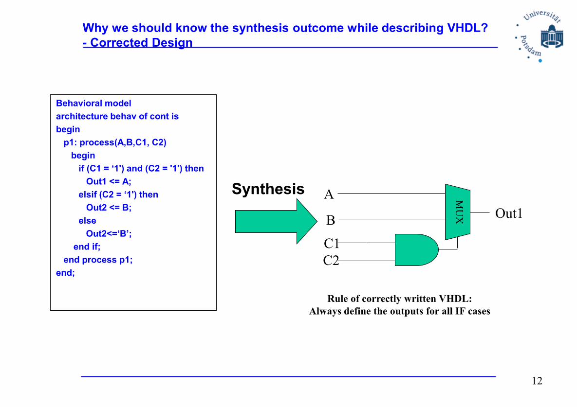
Combining combinational and sequential logic – Alternative approach
library IEEE;
use IEEE.STD_LOGIC_1164.all;
use IEEE.STD_LOGIC_ARITH.ALL;
entity SUB_ex_clk is port (
clk, reset: in std_logic;
in1, in2 : in SIGNED(3 downto 0) ;
out1: out SIGNED(4 downto 0) ) ;
end SUB_ex_clk;
architecture Behav of SUB_ex_clk is
Signal out_s: SIGNED(4 downto 0);
Begin
Out_s<= in1(3)&in1 – in2(3)& in2;
px: process(clk, reset)
if reset=‘1’ then
out1<=(others=>‘0’);
elsif clk’event and clk=‘1’ then
out1<= out_s; -- could we visualize such circuit after synthesis?
end if;
end process px;
end Behav;
; 26

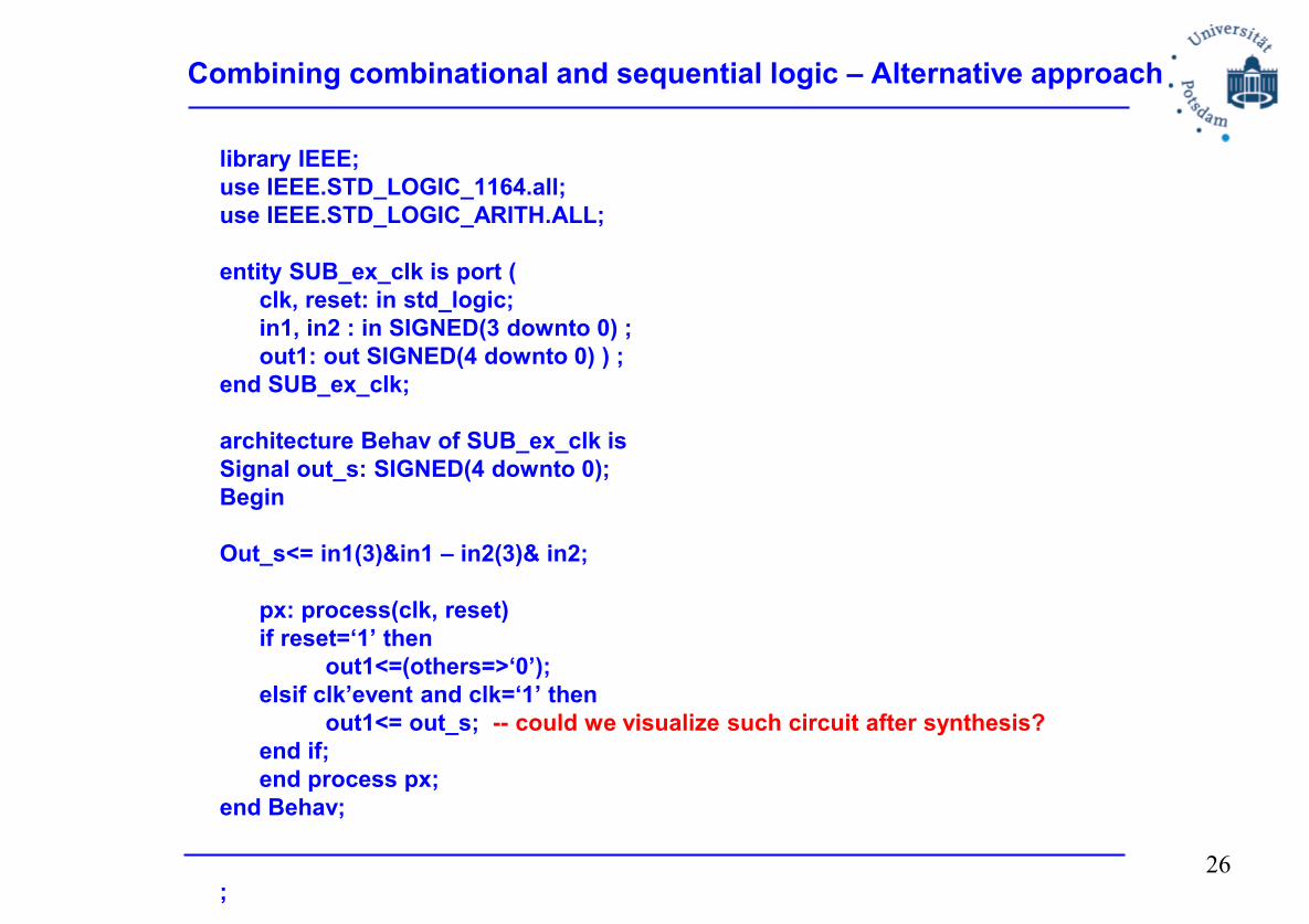
Combining combinational and sequential logic – adding conditions
library IEEE;
use IEEE.STD_LOGIC_1164.all;
use IEEE.STD_LOGIC_ARITH.ALL;
entity ACU_ex_clk is port (
clk, reset, cnt: in std_logic;
in1, in2 : in SIGNED(3 downto 0) ;
out1: out SIGNED(4 downto 0) ) ;
end ACU_ex_clk;
architecture Behav of ACU_ex_clk is
Signal out_s: SIGNED(4 downto 0);
Begin
Out_s<= in1(3)&in1 – in2(3)& in2 when cnt=‘1’ else in1(3)&in1 – in2(3)& in2;
px: process(clk, reset)
if reset=‘1’ then
out1<=(others=>‘0’);
elsif clk’event and clk=‘1’ then
out1<= out_s;
end if;
end process px;
end Behav;
; 27
Combining combinational and sequential logic – adding conditions
library IEEE;
use IEEE.STD_LOGIC_1164.all;
use IEEE.STD_LOGIC_ARITH.ALL;
entity ACU_ex_clk is port (
clk, reset, cnt: in std_logic;
in1, in2 : in SIGNED(3 downto 0) ;
out1: out SIGNED(4 downto 0) ) ;
end ACU_ex_clk;
architecture Behav of ACU_ex_clk is
Signal out_s: SIGNED(4 downto 0);
Begin
px: process(clk, reset)
if reset=‘1’ then
out1<=(others=>‘0’);
elsif clk’event and clk=‘1’ then
case cnt is
when ‘1’ => out1<= in1(3)&in1 – in2(3)& in2;
when others => out1<= in1(3)&in1 + in2(3)& in2;
end case;
end if;
end process px;
end Behav;
; 28

Resource Sharing
process (s1,s2,s3,cnt) begin
if (cnt=‘0’) then
Out1 <= S1 * S2 ;
else
Out1 <= S3 * S2 ;
end if ;
end process ;
29
X
X
MU
X
S1
S2
S3
cnt
X
MU
X
S1
S2
S3
cnt
equivalent
process (s1,s2,s3,cnt) begin
if (cnt=‘0’) then
Out1_s <= S1 ;
else
Out1_s <= S3 ;
end if ;
Out1<= Out1_s*S2;
end process ;

Latches and Flip-flops (reminder)
• Sequential elements are latches and flip-flops
Flip-flops are more frequently used in synchronous designs
• Latches process (EN, D, RSTN) – please check the sensitivity list begin if RSTN=‘0’ then
if (EN = ‘1’) then Q <= D ; end if; end process;
• Flip-flops process (CLK) begin if (CLK’event and CLK= ‘0’) then – what this means? Q <= D ; end if; end process;
30

Reset/Set as synchronous and asynchronous signals
• Asynchronous reset/set corresponds to equivalent flip-flop standard cells where activation/deactivation or reset is not related to clock activity
How to describe this in VHDL?
• Asynchronous signals could be critical in synchronous system since we do not know timing relation to the clock
Metastability issue
Synchronization of reset from the external world
• Synchronous reset behaves as any other signal within the synchronous pipeline.
Could be seen as multiplexer before the flip-flop
More rarely used, often in specific applications (space)
How to describe this in VHDL?
31
D
CLK RST
Q MU
X ‘0’
D Out
D-FF
CLK

Try your examples
• Try with simple circuits:
• 8-bit counter with Load and Asynchronous Reset
• Shift register (Shift left, right, rotate)
• Tri-state buffer
• Bi-directional buffer
Not frequently used for on-chip communication
32
Output Input
En

Moore/Mealy FSMs
http://www.rz.e-technik.fh-kiel.de/~dispert/digital/digital6/dig006_2.htm
Moore Format
Mealy Format
33

State machine synthesis issues
• Two-types of FSM models
Mealy model: outputs = f ( inputs, state)
Moore model: outputs = f ( state )
• Present_state and next_state
Enumeration type
state encoding
• Two processes
combinational and sequential
• Using “case” statement rather than “if-then-elsif…” to avoid generation of priority encoder
• Next state assigned in a synchronous template
34

Models of Synchronous Systems
• Moore and Mealy FSMs
35

Moore Model in VHDL
library IEEE; use IEEE.STD_LOGIC_1164.all;
entity Moore is
port ( Inp1 , clk, reset : in std_logic ;
Out1 : out std_logic );
end Moore;
architecture FSM of Moore is
type state is (s1, s2, s3);
signal present_state , next_state : state;
begin
process ( inp1 , present_state ) begin – combinational part
case present_state is
when s1 => Out1 <= '0'; if ( Inp1 = '1') then next_state <= s3; else next_state <= s2; end if;
when s2 => Out1 <= ‘0'; if ( Inp1 = '1') then next_state <= s3; else next_state <= s1; end if;
when s3 => Out1 <= '1'; next_state <= s1;
end case;
end process;
process (clk, reset) begin -- sequential part
if reset=‘1’ then
present_state<=s1;
if clk=‘1’ and clk’event then
present_state <= next_state ; -- taking the result of combinational logic and storing into reg
end if;
end process;
end FSM ;
36
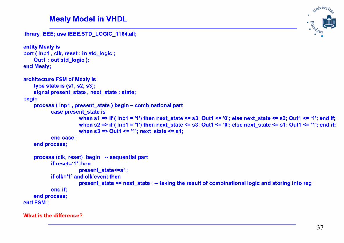
Mealy Model in VHDL
library IEEE; use IEEE.STD_LOGIC_1164.all;
entity Mealy is
port ( Inp1 , clk, reset : in std_logic ;
Out1 : out std_logic );
end Mealy;
architecture FSM of Mealy is
type state is (s1, s2, s3);
signal present_state , next_state : state;
begin
process ( inp1 , present_state ) begin – combinational part
case present_state is
when s1 => if ( Inp1 = '1') then next_state <= s3; Out1 <= '0'; else next_state <= s2; Out1 <= ‘1'; end if;
when s2 => if ( Inp1 = '1') then next_state <= s3; Out1 <= ‘0'; else next_state <= s1; Out1 <= ‘1'; end if;
when s3 => Out1 <= '1'; next_state <= s1;
end case;
end process;
process (clk, reset) begin -- sequential part
if reset=‘1’ then
present_state<=s1;
if clk=‘1’ and clk’event then
present_state <= next_state ; -- taking the result of combinational logic and storing into reg
end if;
end process;
end FSM ;
What is the difference?
37

Memory Synthesis
• Approaches:
Sequential logic using flip-flops or latches
easy to be used, ineffective in respect to area and power
D-flip-flop ~ 26 transistors
Register files in datapaths
SRAM – Static RAM
6 transistors per cell
SRAM memory standard components – no configurability, hard macros
DRAM – only 1 transistor per cell, but needs for refresh
ROM, PROM, Embedded Flash
Emerging memories: RRAM, MRAM, PCRAM
memory compilers – one can choose the configuration and architecture, much
more optimal then FF based, limited number of access ports
Single port, dual-port, two-port memories
38

Memory Generator
Source: Xilinx

Involving memories in Code
• For generating memory models one should use memory generators
• Memory instances should be included in the structural VHDL code
• For memory wrappers (glue logic) generate the separate instance
• Normally for behavioral simulation use VHDL memory models
• For back-annotation use verilog memory models
40

FIFO Implementation
• FIFOs should be implemented as circular buffers
41
RAM
Write pointer
(counter) Read pointer
(counter) we re
W_add R_add
W_data R_data

Combinational and sequential logic – Coding Guidelines
• Avoid the instances with only combinational logic
The output signals should be registered
• For pure combinational path use non-process description style
(dataflow)
• For sequential parts always use flip-flop template
For most of the applications is best to use consistently
asynchronous reset
42

Design Organization & Partitioning
• Don‘t mix structural and behavioral code
Avoid glue logic in structural designs; if necessary put the glue logic in a separate design entity.
• Use comments to describe important issues related to the code functionality.
• Make the header for each entity with corresponding comments
• For large designs try to organise your files to be distributed in separate folders; each folder should contain data related to a larger structural unit of the design.
• Avoid using generics at the top level; it is recommended to use packages with definitions of constants instead of generics
• Make clock dividers and reset synchronisers as separate entities and include them on the top
43

Naming conventions
• Design name and entity name should be the same
example (vhdl): design.vhd; example (verilog): design.v
entity design is module design
• Port, signal, process, and instance names should be meaningful
clk, data, data, reset, ack, cs, wr, rd, test_si, etc
• Don’t mix lower and upper case (however VHDL is not case sensitive)
• For signals and variables that are active low, this shall be clearly
indicated by their name, by suffixing _n
• Every process shall have a name; the name shall be formed by suffixing
_proc
• Architecture name shall be formed by suffixing _arch
44

Architectural Decisions
• When some system is coded on RTL level, the designer has to have
in mind the system architecture
• Memory insertion must be considered
• Area trade-off
• Performance trade-off
• Power trade-off
45

Reset Issue
• Ensure that all the registers in the design are resettable;
Non-resettable registers are not testable and their behaviour is hard
to debug
• If the design requirements prefer non-resettable cells make sure to
provide proper initialisation procedure in the simulation;
• Asynchronous resets are most commonly used
Don’t mix synchronous and asynchronous resets.
• Use reset synchronizers
46

Clocking strategy
• Reasonable clock frequencies are (rule of thumb)
for 0.25 um up to 100 MHz,
for 0.13 um up to 166 MHz.
• If possible avoid different clock domains
• Clock control circuits (gates, divider, multiplexers) should be
grouped in the single entity on the top level of design
• For high performance design or complex clocking (divided clock
domains) use PLL (DLL) in design
• Take care about the delta cycles!
47
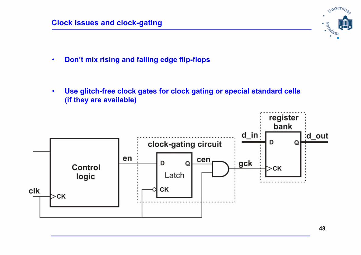
Clock issues and clock-gating
• Don’t mix rising and falling edge flip-flops
• Use glitch-free clock gates for clock gating or special standard cells
(if they are available)
48
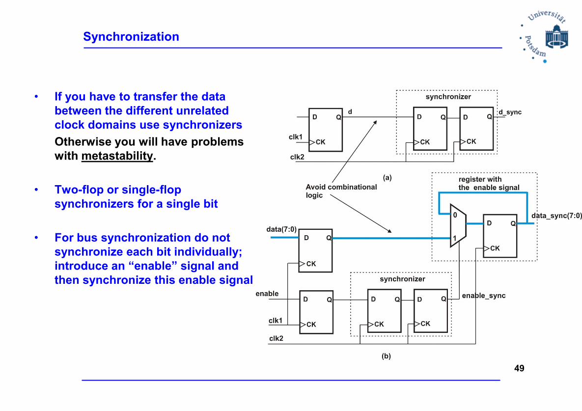
Synchronization
• If you have to transfer the data
between the different unrelated
clock domains use synchronizers
Otherwise you will have problems
with metastability.
• Two-flop or single-flop
synchronizers for a single bit
• For bus synchronization do not
synchronize each bit individually;
introduce an “enable” signal and
then synchronize this enable signal
49

Making design testable
• Provide test_mode signal
In this mode all clocks must come directly from PADs without any
gating
In this mode all reset signals must come directly from PADs without
any gating or registering
• DFT strategies commonly used
Structural test (Scan test)
Memory BIST
Logic BIST
• Advanced rules for memory insertion, combinational loops, reset
definition, complex clocking with DFT
50
Standard and Scan Flip-Flop

Test and Verification
• Writing the good testbench is as much important as making the good
design
• The input data could be read from the file (textio package)
The output data should be compared to the golden model (coming
from C, MATLAB etc.)
• The tests should be as much exhaustive as possible
Code coverage shall be reported to ensure the quality and the
thoroughness of the testbench
• Use assertions and avoid relying on GUI

Conclusions
• Writing a VHDL is not the same as writing C-code
• The designer must understand the concequences of particular
coding style
• The designer should write the code such that this fully defines
resulting hardware after synthesis
• Some guidelines should be followed to have the efficient code
generation
52