Embed Size (px)
Citation preview


VISION Establish technology, business, and education framework for industry, government,
and academia to accelerate transition of integrated photonic solutions from innovation tomanufacturing-ready systems spanning commercial and defense applications.
Building the 21st Century Integrated Silicon
Photonics Ecosystem
You can pack more information onto a light
pipeline than an electric cable, all while
consuming much less power
1600 Gb/sec
metals
gases
chemicals
DNA
pathogens
spectroscopy
LIDAR
tuberculosis
bacteria
MRSA
white / red
blood Cell
DNA
peptides
Improved healthcare
Threats mitigation
Connect the world
More energy efficient
Defense
Data Comm / Telecom PIC Sensors
data transmission
Integrated Photonics
is about data
and sensing
Obstacle detection
Lighter and faster
Small / cost effective / reliable
Very low power
Continuously Tunable Optical Orbital Angular Momentum Generator
Augmented Reality
Robotics

Close the gap between research & commercial production
Headquarters – NY Lead – SUNY Poly, Albany
NY Nationwide Collaboration
– interest in 33 States Over 80 Members
© Copyright 2017 AIM Photonics Proprietary
and Confidential
Integrated Photonics; IV-IV CMOS, III-V and SiPh technology functionality(s) integration to enable advanced product / system performance
Manufacturing Technologies which enable novel, leading edge product/system solutions

Integrated Photonics Market Environment
’Hockey Stick’
Characteristic
5yrs slow growth
mature technology
overcome
manufacturability issues
3yrs to product
commercialization
then exponential growth
rapid adaption
iPhotonics Market Characteristics
34
79
24
18 1
2015138 M$
0.8
4.0
3.0
0.7
20208.6 B$
4.6
54.1
4.1
36.9
8.2
2025108 B$
22
20
2
9
201054 M$
AnalogRFApplications
DataCom/Telecom
PICArrayTechnologies
PICSensors
Scientific,Aero,Defense
Others
22
20
2
9
201054 M$
AnalogRFApplications
DataCom/Telecom
PICArrayTechnologies
PICSensors
Scientific,Aero,Defense
Others
22
20
2
9
201054 M$
AnalogRFApplications
DataCom/Telecom
PICArrayTechnologies
PICSensors
Scientific,Aero,Defense
Others
DataCom / Telecom Industry driven / Aggressive
Drive Solutions on-the-way Continuous / fast migration to
iPhotonics
Arrays / RF Analog Defense Industry driven / Virgin
Territories Solutions evolve Slow migration to iPhotonics
Sensors Bio / Healthcare, total lack of adaption to Si-Technology Solutions iPhotonics will be of disruptive nature (molecular diagnostics) Solutions (spectroscopy) to be driven in collaboration with
Department-of-Health & Player that intends to jump into the market ‘big’
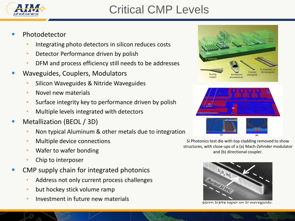
Critical CMP Levels
Photodetector
• Integrating photo detectors in silicon reduces costs
• Detector Performance driven by polish
• DFM and process efficiency still needs to be addresses
Waveguides, Couplers, Modulators
• Silicon Waveguides & Nitride Waveguides
• Novel new materials
• Surface integrity key to performance driven by polish
• Multiple levels integrated with detectors
Metallization (BEOL / 3D)
• Non typical Aluminum & other metals due to integration
• Multiple device connections
• Wafer to wafer bonding
• Chip to interposer
CMP supply chain for integrated photonics
• Address not only current process challenges
• but hockey stick volume ramp
• Investment in future new materials
Si Photonics test die with top cladding removed to showstructures, with close-ups of a (a) Mach-Zehnder modulator
and (b) directional coupler.

2016 PROJECT PORTFOLIOKTMA/MCE PROJECT NAME
Datacom High Capacity High Radix Optical SwitchAnalog RF Integrated Photonic Analog Link on SiPIC Sensors Raman Chem/BioEPDA EPDA PDKEPDA DFM Methods and Tools MPWA Laser Integration into SUNY Platform with HeteroepitaxyMPWA Chip Level Packaging, Year 1 Pilot PhaseMPWA PIC Integration on Interposer & ChipMPWA 300mm MPWA Program, Year 1 Pilot PhaseICT Inline Controls & Testing, Year 1 Pilot Project
TAPFunctional Testing Development for Automated Scaled Manufacturing
TAP High Density Fiber-Chip IO Packaging TAP High-throughput Mfg. for PIC Polymer WG ConnectionPIC Sensors Waveguide SPRTAP Rochester HubAnalog RF Integrated Photonic Analog Link and Processing on InPEPDA InP EPDA ToolsMPWA InP PIC FoundryPIC Array Free Space Communications
Projects

Potential CMP Project Example for AIM Photonics
• Uniformity across that length• Not just height but smoothness• CMP Absolutely critical for this device• How to solve this problem
REQUIRES Multiple Partners• Design / Simulation: PDK• Silicon / Fabrication: MPW• Process solution via:
• DFM Predictability• Committed Consumable Supply• Final Manufacturing solution
QUALIFIED SUPPLY CHAIN!

Silicon Photonics Process Design Kits (PDK)
PDK– 3 technologies, 2 major releases/year• Full (active)- v1.0 available now• Passive- v1.0 available now• Interposer- v1.0 available now• Next: v1.5 (Aug’17), v2.0 (Jan’18)• Incremental releases add components &
maturity leading to guaranteed specs based on full statistical corner validation
Extensive Component Library• Passive, Active and Interposer components• Support for simulation, layout,
schematics, DRC, documentation• Developed by Analog Photonics LLC
(Boston) EDA/PDA Design Software Supported
Download the PDK from MOSIS• AIM Membership or license required
8
PDK Passive Components Qty Selected Performance
Waveguides (Si & SiN), curves,
etc.16+ Si:<2.2dB/cm, SiN:<1dB/cm
Edge Couplers (Si & SiN) 2 <2.5dB/facet loss
Vertical Couplers (Si & SiN) 2 <3dB loss
3dB 4-Port Couplers (Si & SiN) 2 loss <0.5dB, deviation <1%
Y- Junctions (Si & SiN) 2 loss <0.25dB, deviation <1%
Directional Coupler (Si & SiN) 2loss <0.5dB, deviation <1% @
1550nm
Si-to-SiN Coupler (escalator) 1 loss <0.1dB
Crossing (Si) 1 loss <0.25dB, crosstalk < -60dB
PDK Active Devices Qty Selected Performance
Digital Ge Photodetector 1 >30GHz, <20nA dark
Analog Ge Photodetector 1 >25GHz, <80nA dark
Digital Mach-Zehnder
Modulator1
>15GHz, >25Gb/s, push-pull
<2Vpp per arm, >5dB extinction,
<5dB loss
Analog Mach-Zehnder
Modulator1
>15GHz, -10V< Vs <0V, 25dB lin.,
1500–1600 nm
Thermo-Optic Phase Shifter (Si) 10.25dB loss, <50mW,
range 0π<Δθ<2π
Thermo-Optic Switch (Si) 1 <1dB loss, 25mW
Tunable Filter (Si) 4<0.5dB loss, 26nm FSR,
>1nm/mW tuning efficiency
Microdisk Switch (tunable) 4<2ns switch time,
>200GHz EO tuning @ 1.2V
Microdisk Modulator (tunable) 415GHz, 25Gb/s, 1.2Vpp, 1dB Loss,
8dB extinction

Silicon Photonics Multi Project Wafer (MPW)
MPW Fab Runs Planned in 2017 • SUNY Poly 300mm fab line• 3 MPW offerings
• Full-Active- 2 planned in 2017• Passive Only- 2 planned in 2017• Interposer- 1 planned in 2017
• Reservations to be a rider can be started athttp://www.aimphotonics.com/pdk-mpw-sign-up/
• Generates quote with terms• 20% down to hold slot; balance invoiced at
design submission MOSIS is the MPW Aggregator
• DRC clean designs are submitted to MOSIS• MOSIS also distributes the PDK
MPW Pricing
PASSIVE• 50mm2 chips• $30K AIM members• $36K non-members
FULL• 50mm2 chips
• $100K AIM members • $120K non-members
• 8mm2 chips• $25K AIM members • $30K non-members
INTERPOSER• 156mm2• $93.6K AIM members• $112.3K non-members

Now is time to be involved in the solution
Dies attached to a 300mm photonic interposer waferat SUNY Poly
500 Gb/sec Infinera InP transceiver
Intel integrated 4x25Gbps technology, with hybrid silicon lasers
IBM 5nm chip uses a "gate-all-around" transistor (GAAFET)
$100B