Embed Size (px)
Citation preview
Vivado Design Suite
Tutorial Designing IP Subsystems Using IP
Integrator
UG995 (v 2013.3) October 2, 2013

Notice of Disclaimer
The information disclosed to you hereunder (the "Materials") is provided solely for the selection and use of Xilinx products. To the
maximum extent permitted by applicable law: (1) Materials are made available "AS IS" and with all faults, Xilinx hereby DISCLAIMS
ALL WARRANTIES AND CONDITIONS, EXPRESS, IMPLIED, OR STATUTORY, INCLUDING BUT NOT LIMITED TO WARRANTIES OF
MERCHANTABILITY, NON-INFRINGEMENT, OR FITNESS FOR ANY PARTICULAR PURPOSE; and (2) Xilinx shall not be liable (whether
in contract or tort, including negligence, or under any other theory of liability) for any loss or damage of any kind or nature related
to, arising under, or in connection with, the Materials (including your use of the Materials), including for any direct, indirect, special,
incidental, or consequential loss or damage (including loss of data, profits, goodwill, or any type of loss or damage suffered as a
result of any action brought by a third party) even if such damage or loss was reasonably foreseeable or Xilinx had been advised of
the possibility of the same. Xilinx assumes no obligation to correct any errors contained in the Materials or to notify you of updates
to the Materials or to product specifications. You may not reproduce, modify, distribute, or publicly display the Materials without
prior written consent. Certain products are subject to the terms and conditions of the Limited Warranties which can be viewed at
http://www.xilinx.com/warranty.htm; IP cores may be subject to warranty and support terms contained in a license issued to you by
Xilinx. Xilinx products are not designed or intended to be fail-safe or for use in any application requiring fail-safe performance; you
assume sole risk and liability for use of Xilinx products in Critical Applications: http://www.xilinx.com/warranty.htm#critapps.
©Copyright 2013 Xilinx, Inc. Xilinx, the Xilinx logo, Artix, Vivado, ISE, Kintex, Spartan, Virtex, Vivado, Zynq, and other designated
brands included herein are trademarks of Xilinx in the United States and other countries. All other trademarks are the property of
their respective owners...
Revision History
Date Version Revision
10/02/2013 2013.3 Validated with release.
06/20/2013 2013.2 Minor editorial update.
06/19/2013 2013.2 New in this release.
Designing IP Subsystems Using IP Integrator www.xilinx.com 3
UG995 (v 2013.3) October 2, 2013
Table of Contents
Revision History........................................................................................................................................................... 2
Table of Contents ............................................................................................................................................................ 3
Designing IP Subsystems ............................................................................................................................................. 4
Introduction .................................................................................................................................................................. 4
Tutorial Design Description .................................................................................................................................... 4
Software Requirements ............................................................................................................................................ 4
Hardware Requirements .......................................................................................................................................... 5
Locating Tutorial Design Files ................................................................................................................................ 5
Lab 1: Designing IP Subsystems in IP Integrator................................................................................................. 6
Step 1: Creating a Project ........................................................................................................................................ 6
Step 3: Creating External Connections ............................................................................................................ 13
Step 4: Customize IP ............................................................................................................................................... 19
Step 5: Running Connection Automation ...................................................................................................... 22
Step 6: Using the Address Editor ....................................................................................................................... 28
Step 7: Creating and Implementing the Top-Level Design ..................................................................... 30
Conclusion .................................................................................................................................................................. 34
Send Feedback
Designing IP Subsystems Using IP Integrator www.xilinx.com 4
UG995 (v 2013.3) October 2, 2013
Designing IP Subsystems
Introduction
The Xilinx® Vivado® Design Suite IP integrator feature lets you create complex system designs
by instantiating and interconnecting IP cores from the Vivado IP catalog onto a design canvas.
You can create designs interactively through the IP integrator design canvas GUI, or
programmatically using a Tcl programming interface. You will typically construct designs at the
AXI interface level for greater productivity; but you may also manipulate designs at the port level
for more precise design control.
This tutorial walks you through the steps for building a basic IP subsystem design using the IP
Integrator tool. You will instantiate a few IP in the IP Integrator tool and then stitch them up to
create an IP sub-system design. While working on this tutorial, you will be introduced to the IP
Integrator GUI, run design rule checks (DRC) on your design, and then integrate the design in a
top-level design in the Vivado Design Suite. Finally, you will run synthesis and implementation
and generate bitstream on the design.
TIP: You can also learn more about the Vivado Design Suite IP integrator feature by
viewing the quick take video at http://www.xilinx.com/csi/training/vivado/designing-with-
vivado-ip-integrator.htm.
Tutorial Design Description
This tutorial is based on a simple non-processor based IP Integrator design. It contains a few
peripheral IP cores, and an AXI interconnect core, which connects to an external on-board
processor.
The design targets a xc7k325 Kintex device. A small design is used to allow the tutorial to be run
with minimal hardware requirements and to enable timely completion of the tutorial, as well as
to minimize the data size.
Software Requirements
This tutorial requires that the 2013.3 Vivado Design Suite software release or later is installed.
For installation instructions and information, see the Vivado Design Suite User Guide: Release
Notes, Installation, and Licensing (UG973).
Send Feedback
Hardware Requirements
Designing IP Subsystems Using IP Integrator www.xilinx.com 5
UG995 (v 2013.3) October 2, 2013
Hardware Requirements
The supported Operating Systems include Redhat 5.6 Linux 64 and 32 bit, and Windows 7, 64
and 32 bit.
Xilinx recommends a minimum of 2 GB of RAM when using the Vivado tool.
Locating Tutorial Design Files
You can find the files for this tutorial in the Vivado Design Suite examples directory at the
following location:
<Vivado_install_area>/Vivado/<version>/examples/Vivado_Tutorial
You can also extract the provided zip file, at any time, to write the tutorial files to your local
directory, or to restore the files to their starting condition.
Extract the zip file contents from the software installation into any write-accessible location.
<Vivado_install_area>/Vivado/<version>/examples/Vivado_Tutorial.zip
The location of the extracted Vivado_Tutorial directory is referred to as the <Extract_Dir> in this
Tutorial.
Send Feedback
Step 1: Creating a Project
Designing IP Subsystems Using IP Integrator www.xilinx.com 6
UG995 (v 2013.3) October 2, 2013
Lab 1: Designing IP Subsystems in IP
Integrator
Step 1: Creating a Project
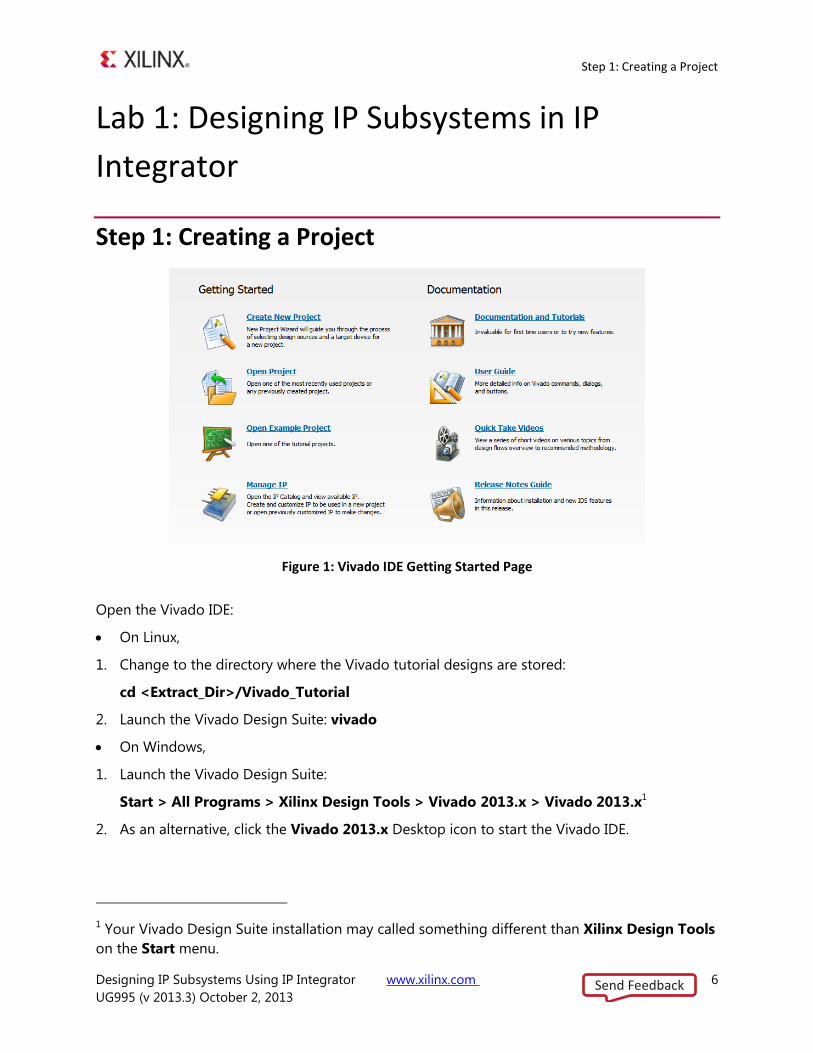
Figure 1: Vivado IDE Getting Started Page
Open the Vivado IDE:
On Linux,
Change to the directory where the Vivado tutorial designs are stored: 1.
cd <Extract_Dir>/Vivado_Tutorial
Launch the Vivado Design Suite: vivado 2.
On Windows,
Launch the Vivado Design Suite: 1.
Start > All Programs > Xilinx Design Tools > Vivado 2013.x > Vivado 2013.x1
As an alternative, click the Vivado 2013.x Desktop icon to start the Vivado IDE. 2.
1 Your Vivado Design Suite installation may called something different than Xilinx Design Tools
on the Start menu.
Send Feedback
Step 1: Creating a Project
Designing IP Subsystems Using IP Integrator www.xilinx.com 7
UG995 (v 2013.3) October 2, 2013
The Vivado IDE Getting Started page contains links to open or create projects and to view
documentation, as shown in Figure 1.
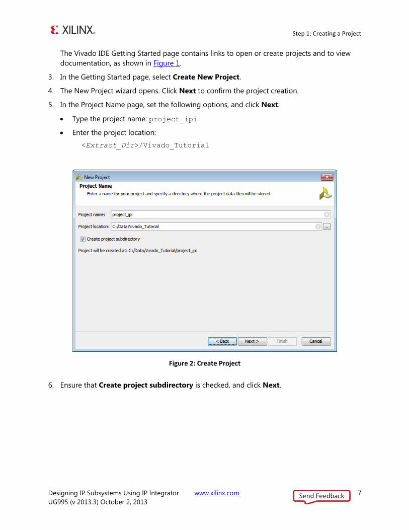
In the Getting Started page, select Create New Project. 3.
The New Project wizard opens. Click Next to confirm the project creation. 4.
In the Project Name page, set the following options, and click Next: 5.
Type the project name: project_ipi
Enter the project location:
<Extract_Dir>/Vivado_Tutorial
Figure 2: Create Project
Ensure that Create project subdirectory is checked, and click Next. 6.
Send Feedback
Step 1: Creating a Project
Designing IP Subsystems Using IP Integrator www.xilinx.com 8
UG995 (v 2013.3) October 2, 2013
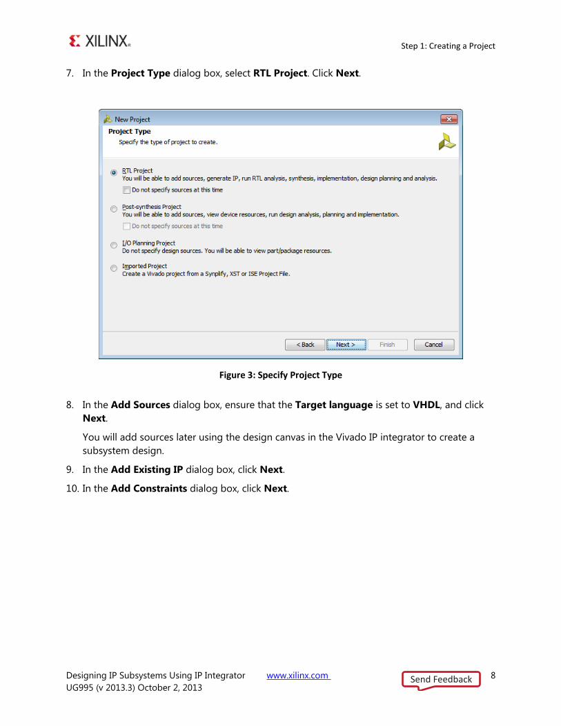
In the Project Type dialog box, select RTL Project. Click Next. 7.
Figure 3: Specify Project Type
In the Add Sources dialog box, ensure that the Target language is set to VHDL, and click 8.
Next.
You will add sources later using the design canvas in the Vivado IP integrator to create a
subsystem design.
In the Add Existing IP dialog box, click Next. 9.
In the Add Constraints dialog box, click Next. 10.
Send Feedback
Step 1: Creating a Project
Designing IP Subsystems Using IP Integrator www.xilinx.com 9
UG995 (v 2013.3) October 2, 2013
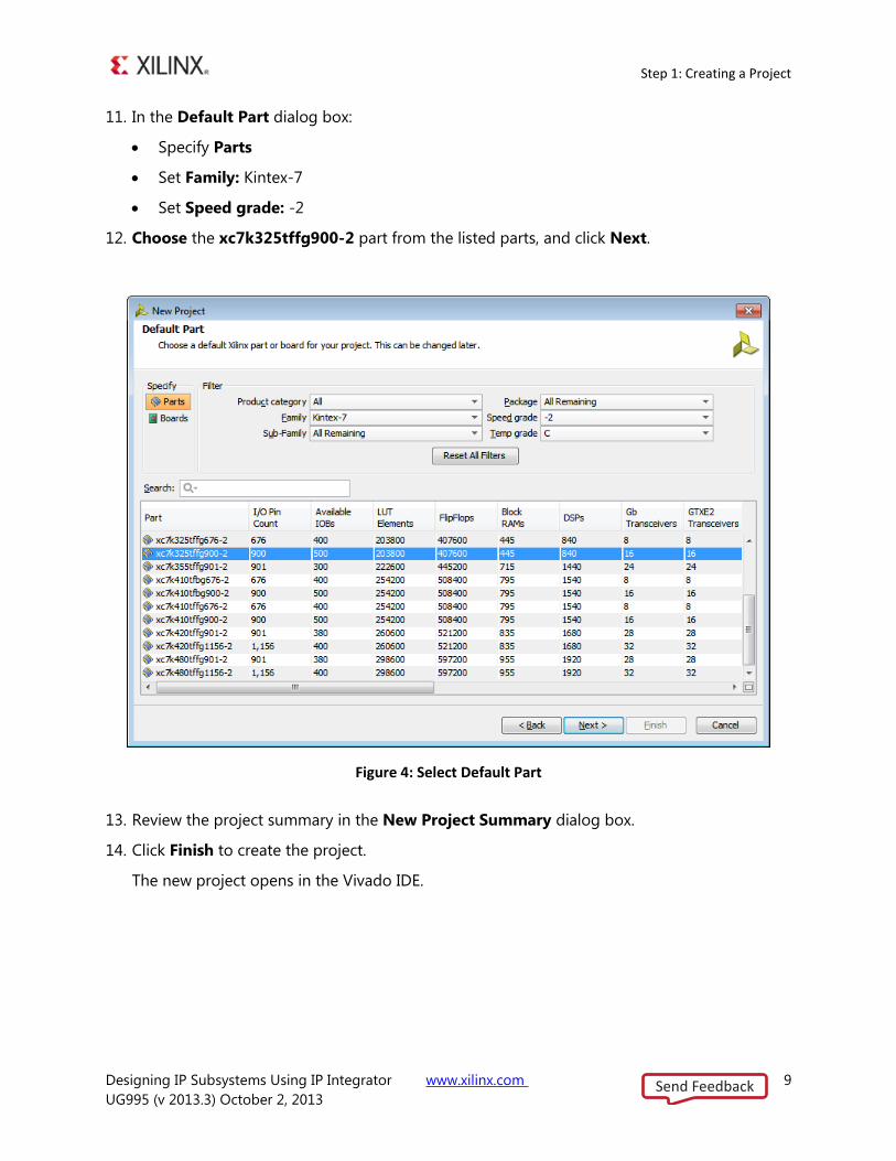
In the Default Part dialog box: 11.
Specify Parts
Set Family: Kintex-7
Set Speed grade: -2
Choose the xc7k325tffg900-2 part from the listed parts, and click Next. 12.
Figure 4: Select Default Part
Review the project summary in the New Project Summary dialog box. 13.
Click Finish to create the project. 14.
The new project opens in the Vivado IDE.
Send Feedback
Step 1: Creating a Project
Designing IP Subsystems Using IP Integrator www.xilinx.com 10
UG995 (v 2013.3) October 2, 2013
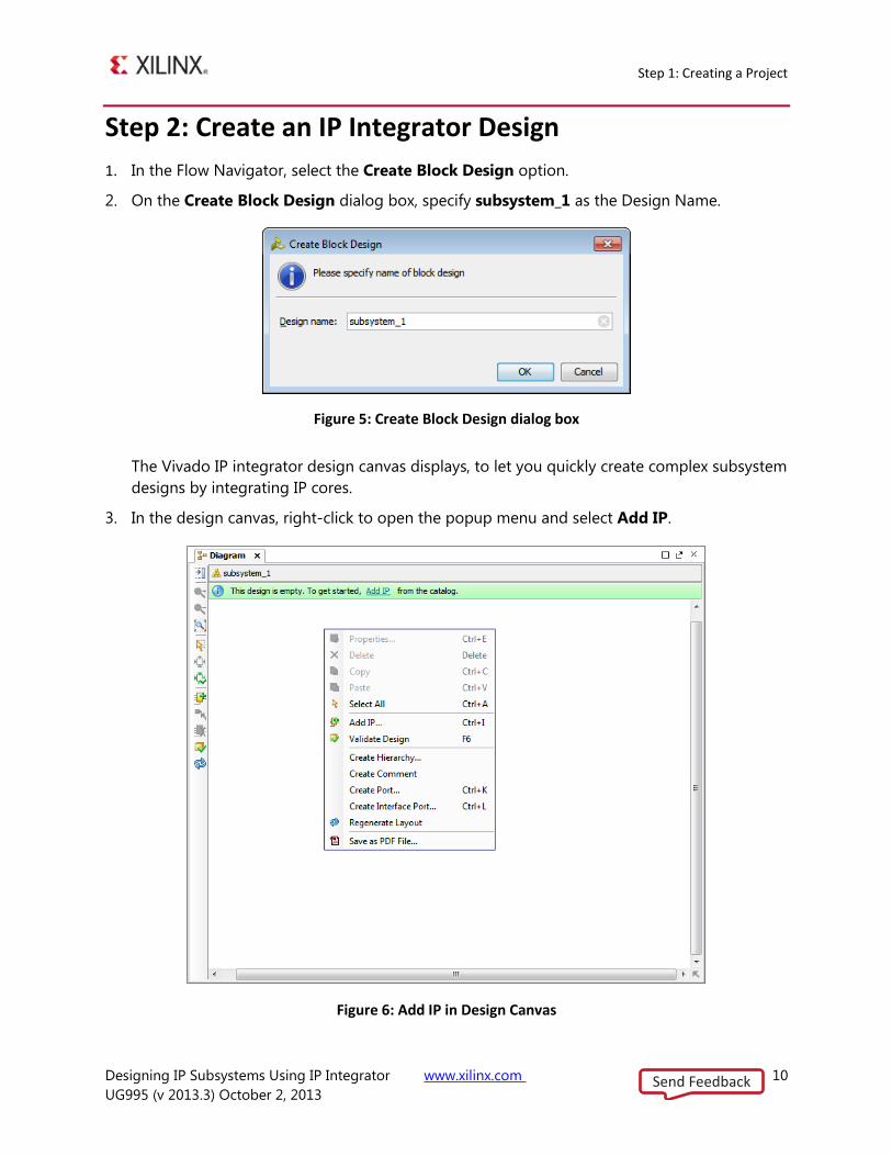
Step 2: Create an IP Integrator Design
In the Flow Navigator, select the Create Block Design option. 1.
On the Create Block Design dialog box, specify subsystem_1 as the Design Name. 2.
Figure 5: Create Block Design dialog box
The Vivado IP integrator design canvas displays, to let you quickly create complex subsystem
designs by integrating IP cores.
In the design canvas, right-click to open the popup menu and select Add IP. 3.
Figure 6: Add IP in Design Canvas
Send Feedback
Step 1: Creating a Project
Designing IP Subsystems Using IP Integrator www.xilinx.com 11
UG995 (v 2013.3) October 2, 2013
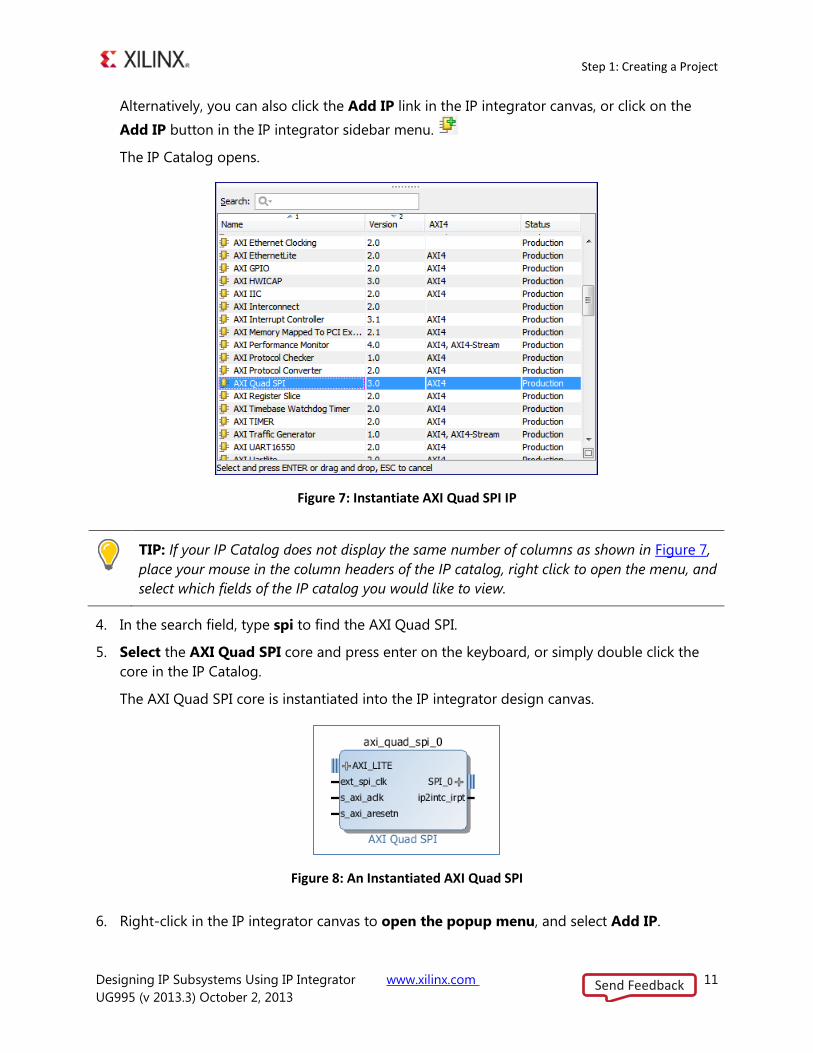
Alternatively, you can also click the Add IP link in the IP integrator canvas, or click on the
Add IP button in the IP integrator sidebar menu.
The IP Catalog opens.
Figure 7: Instantiate AXI Quad SPI IP
TIP: If your IP Catalog does not display the same number of columns as shown in Figure 7,
place your mouse in the column headers of the IP catalog, right click to open the menu, and
select which fields of the IP catalog you would like to view.
In the search field, type spi to find the AXI Quad SPI. 4.
Select the AXI Quad SPI core and press enter on the keyboard, or simply double click the 5.
core in the IP Catalog.
The AXI Quad SPI core is instantiated into the IP integrator design canvas.
Figure 8: An Instantiated AXI Quad SPI
Right-click in the IP integrator canvas to open the popup menu, and select Add IP. 6.
Send Feedback
Step 1: Creating a Project
Designing IP Subsystems Using IP Integrator www.xilinx.com 12
UG995 (v 2013.3) October 2, 2013
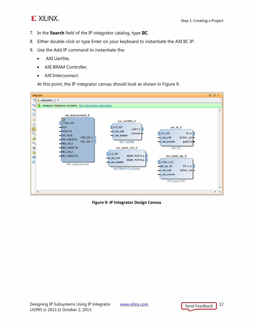
In the Search field of the IP integrator catalog, type IIC. 7.
Either double-click or type Enter on your keyboard to instantiate the AXI IIC IP. 8.
Use the Add IP command to instantiate the: 9.
AXI Uartlite,
AXI BRAM Controller,
AXI Interconnect.
At this point, the IP integrator canvas should look as shown in Figure 9.
Figure 9: IP Integrator Design Canvas
Send Feedback
Step 3: Creating External Connections
Designing IP Subsystems Using IP Integrator www.xilinx.com 13
UG995 (v 2013.3) October 2, 2013
Step 3: Creating External Connections
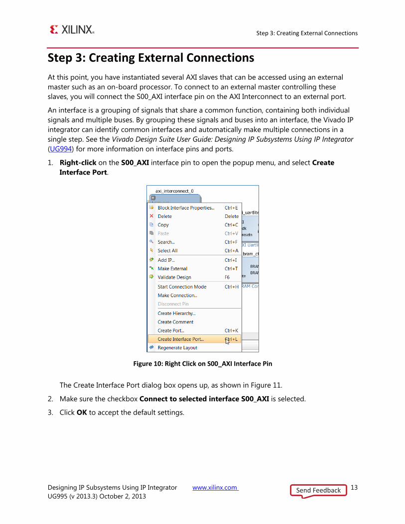
At this point, you have instantiated several AXI slaves that can be accessed using an external
master such as an on-board processor. To connect to an external master controlling these
slaves, you will connect the S00_AXI interface pin on the AXI Interconnect to an external port.
An interface is a grouping of signals that share a common function, containing both individual
signals and multiple buses. By grouping these signals and buses into an interface, the Vivado IP
integrator can identify common interfaces and automatically make multiple connections in a
single step. See the Vivado Design Suite User Guide: Designing IP Subsystems Using IP Integrator
(UG994) for more information on interface pins and ports.
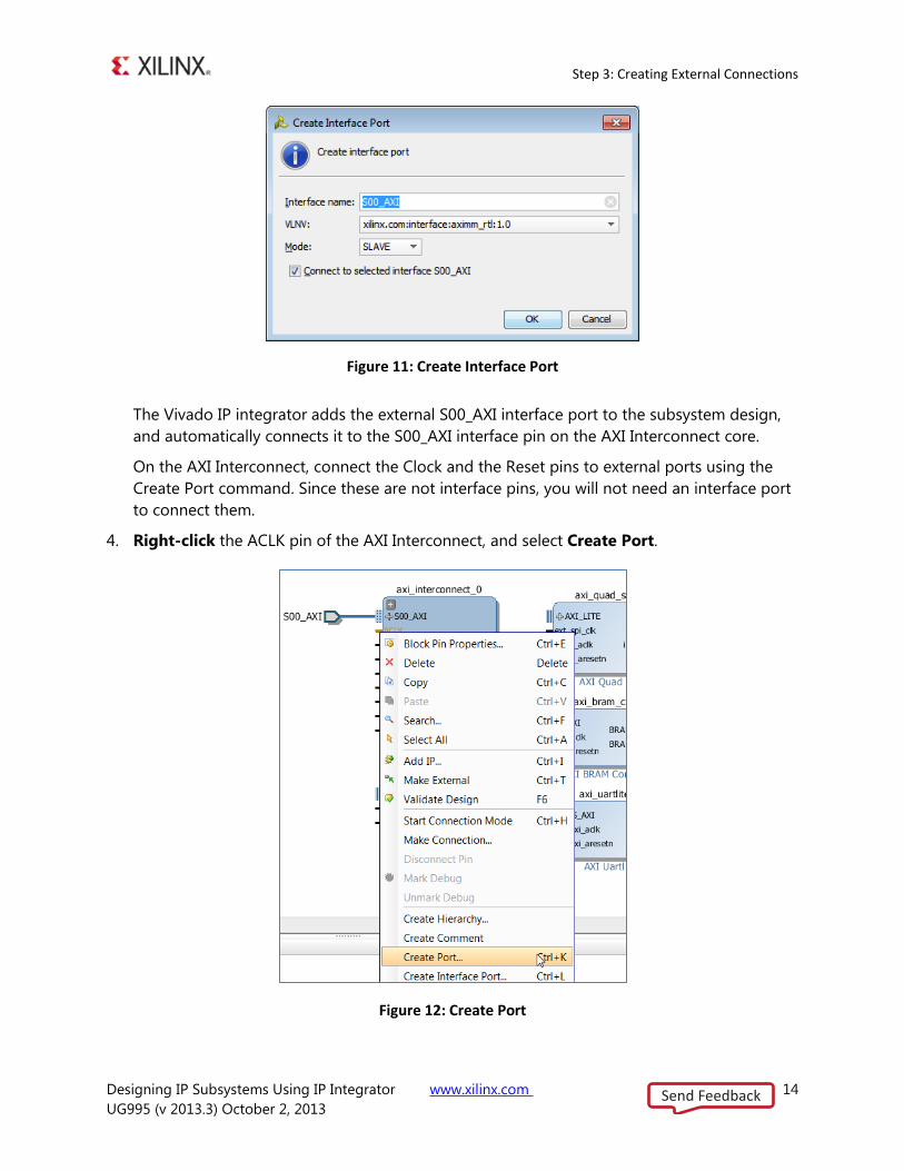
Right-click on the S00_AXI interface pin to open the popup menu, and select Create 1.
Interface Port.
Figure 10: Right Click on S00_AXI Interface Pin
The Create Interface Port dialog box opens up, as shown in Figure 11.
Make sure the checkbox Connect to selected interface S00_AXI is selected. 2.
Click OK to accept the default settings. 3.
Send Feedback
Step 3: Creating External Connections
Designing IP Subsystems Using IP Integrator www.xilinx.com 14
UG995 (v 2013.3) October 2, 2013
Figure 11: Create Interface Port
The Vivado IP integrator adds the external S00_AXI interface port to the subsystem design,
and automatically connects it to the S00_AXI interface pin on the AXI Interconnect core.
On the AXI Interconnect, connect the Clock and the Reset pins to external ports using the
Create Port command. Since these are not interface pins, you will not need an interface port
to connect them.
Right-click the ACLK pin of the AXI Interconnect, and select Create Port. 4.
Figure 12: Create Port
Send Feedback
Step 3: Creating External Connections
Designing IP Subsystems Using IP Integrator www.xilinx.com 15
UG995 (v 2013.3) October 2, 2013
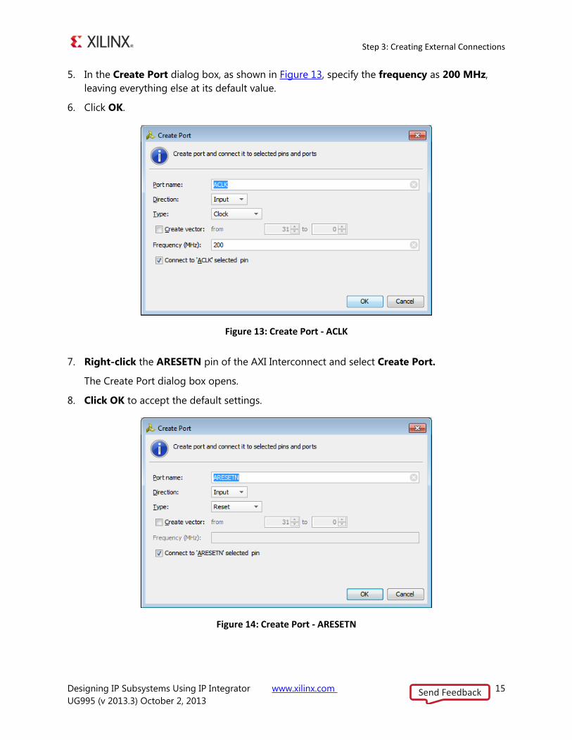
In the Create Port dialog box, as shown in Figure 13, specify the frequency as 200 MHz, 5.
leaving everything else at its default value.
Click OK. 6.
Figure 13: Create Port - ACLK
Right-click the ARESETN pin of the AXI Interconnect and select Create Port. 7.
The Create Port dialog box opens.
Click OK to accept the default settings. 8.
Figure 14: Create Port - ARESETN
Send Feedback
Step 3: Creating External Connections
Designing IP Subsystems Using IP Integrator www.xilinx.com 16
UG995 (v 2013.3) October 2, 2013
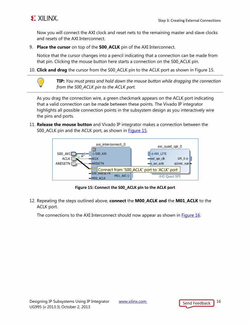
Now you will connect the AXI clock and reset nets to the remaining master and slave clocks
and resets of the AXI Interconnect.
Place the cursor on top of the S00_ACLK pin of the AXI Interconnect. 9.
Notice that the cursor changes into a pencil indicating that a connection can be made from
that pin. Clicking the mouse button here starts a connection on the S00_ACLK pin.
Click and drag the cursor from the S00_ACLK pin to the ACLK port as shown in Figure 15. 10.
TIP: You must press and hold down the mouse button while dragging the connection
from the S00_ACLK pin to the ACLK port.
As you drag the connection wire, a green checkmark appears on the ACLK port indicating
that a valid connection can be made between these points. The Vivado IP integrator
highlights all possible connection points in the subsystem design as you interactively wire
the pins and ports.
Release the mouse button and Vivado IP integrator makes a connection between the 11.
S00_ACLK pin and the ACLK port, as shown in Figure 15.
Figure 15: Connect the S00_ACLK pin to the ACLK port
Repeating the steps outlined above, connect the M00_ACLK and the M01_ACLK to the 12.
ACLK port.
The connections to the AXI Interconnect should now appear as shown in Figure 16.
Send Feedback
Step 3: Creating External Connections
Designing IP Subsystems Using IP Integrator www.xilinx.com 17
UG995 (v 2013.3) October 2, 2013
Figure 16: ACLK connections
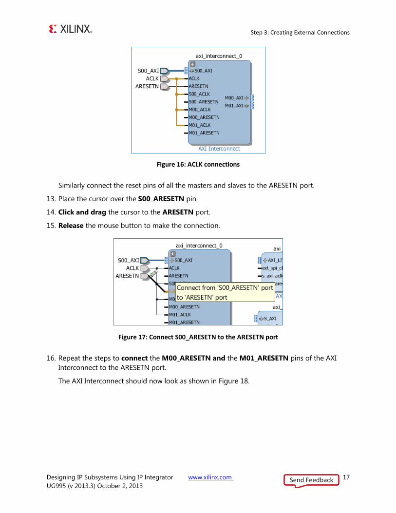
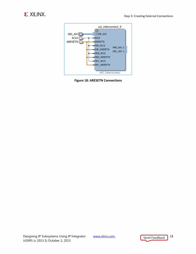
Similarly connect the reset pins of all the masters and slaves to the ARESETN port.
Place the cursor over the S00_ARESETN pin. 13.
Click and drag the cursor to the ARESETN port. 14.
Release the mouse button to make the connection. 15.
Figure 17: Connect S00_ARESETN to the ARESETN port
Repeat the steps to connect the M00_ARESETN and the M01_ARESETN pins of the AXI 16.
Interconnect to the ARESETN port.
The AXI Interconnect should now look as shown in Figure 18.
Send Feedback
Step 3: Creating External Connections
Designing IP Subsystems Using IP Integrator www.xilinx.com 18
UG995 (v 2013.3) October 2, 2013
Figure 18: ARESETN Connections
Send Feedback
Step 4: Customize IP
Designing IP Subsystems Using IP Integrator www.xilinx.com 19
UG995 (v 2013.3) October 2, 2013
Step 4: Customize IP
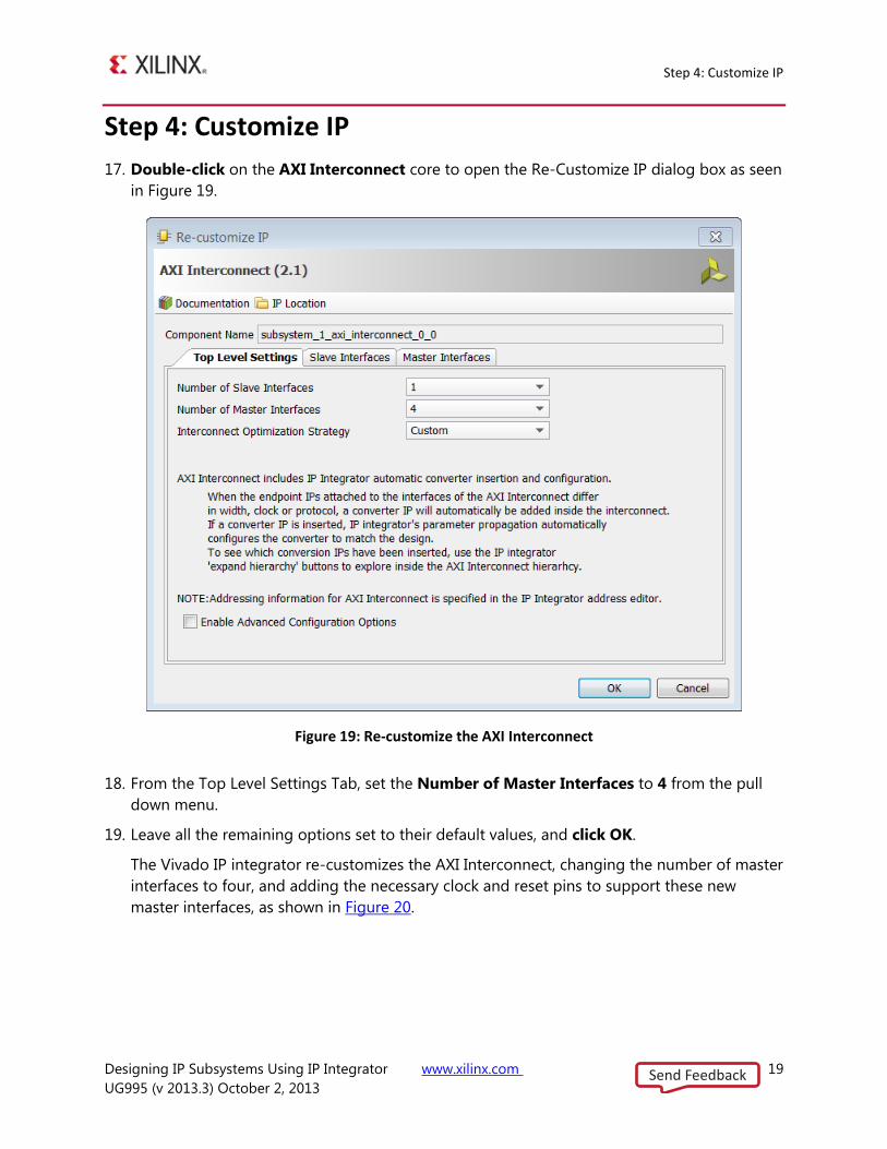
Double-click on the AXI Interconnect core to open the Re-Customize IP dialog box as seen 17.
in Figure 19.
Figure 19: Re-customize the AXI Interconnect
From the Top Level Settings Tab, set the Number of Master Interfaces to 4 from the pull 18.
down menu.
Leave all the remaining options set to their default values, and click OK. 19.
The Vivado IP integrator re-customizes the AXI Interconnect, changing the number of master
interfaces to four, and adding the necessary clock and reset pins to support these new
master interfaces, as shown in Figure 20.
Send Feedback
Step 4: Customize IP
Designing IP Subsystems Using IP Integrator www.xilinx.com 20
UG995 (v 2013.3) October 2, 2013
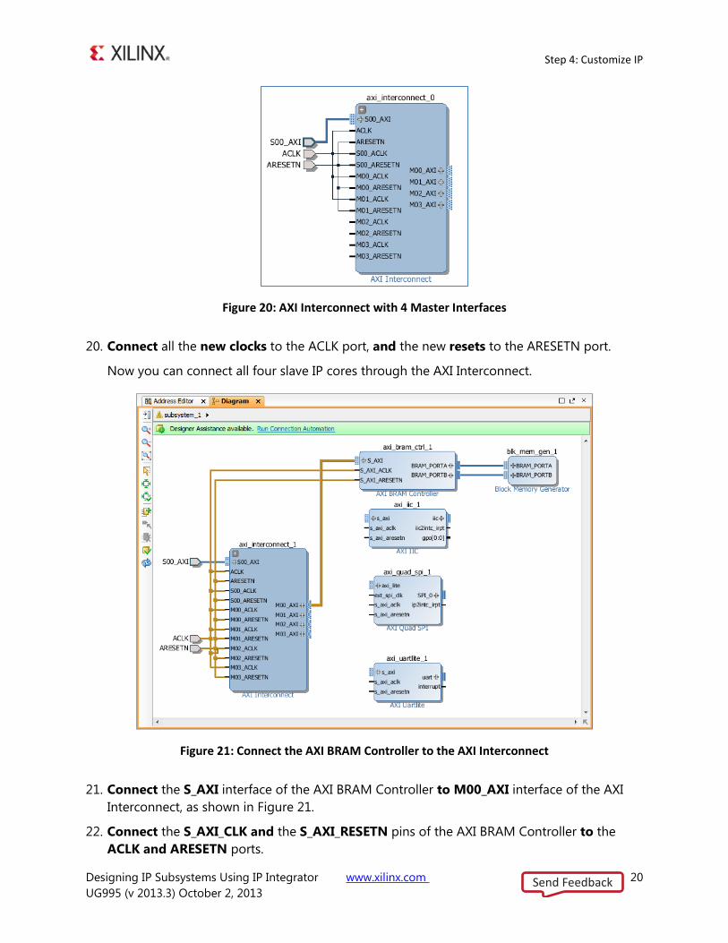
Figure 20: AXI Interconnect with 4 Master Interfaces
Connect all the new clocks to the ACLK port, and the new resets to the ARESETN port. 20.
Now you can connect all four slave IP cores through the AXI Interconnect.
Figure 21: Connect the AXI BRAM Controller to the AXI Interconnect
Connect the S_AXI interface of the AXI BRAM Controller to M00_AXI interface of the AXI 21.
Interconnect, as shown in Figure 21.
Connect the S_AXI_CLK and the S_AXI_RESETN pins of the AXI BRAM Controller to the 22.
ACLK and ARESETN ports.
Send Feedback
Step 4: Customize IP
Designing IP Subsystems Using IP Integrator www.xilinx.com 21
UG995 (v 2013.3) October 2, 2013
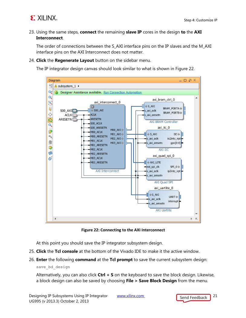
Using the same steps, connect the remaining slave IP cores in the design to the AXI 23.
Interconnect.
The order of connections between the S_AXI interface pins on the IP slaves and the M_AXI
interface pins on the AXI Interconnect does not matter.
Click the Regenerate Layout button on the sidebar menu. 24.
The IP integrator design canvas should look similar to what is shown in Figure 22.
Figure 22: Connecting to the AXI Interconnect
At this point you should save the IP integrator subsystem design.
Click the Tcl console at the bottom of the Vivado IDE to make it the active window. 25.
Enter the following command at the Tcl prompt to save the current subsystem design: 26.
save_bd_design
Alternatively, you can also click Ctrl + S on the keyboard to save the block design. Likewise,
a block design can also be saved by choosing File > Save Block Design from the menu.
Send Feedback
Step 5: Running Connection Automation
Designing IP Subsystems Using IP Integrator www.xilinx.com 22
UG995 (v 2013.3) October 2, 2013
Step 5: Running Connection Automation
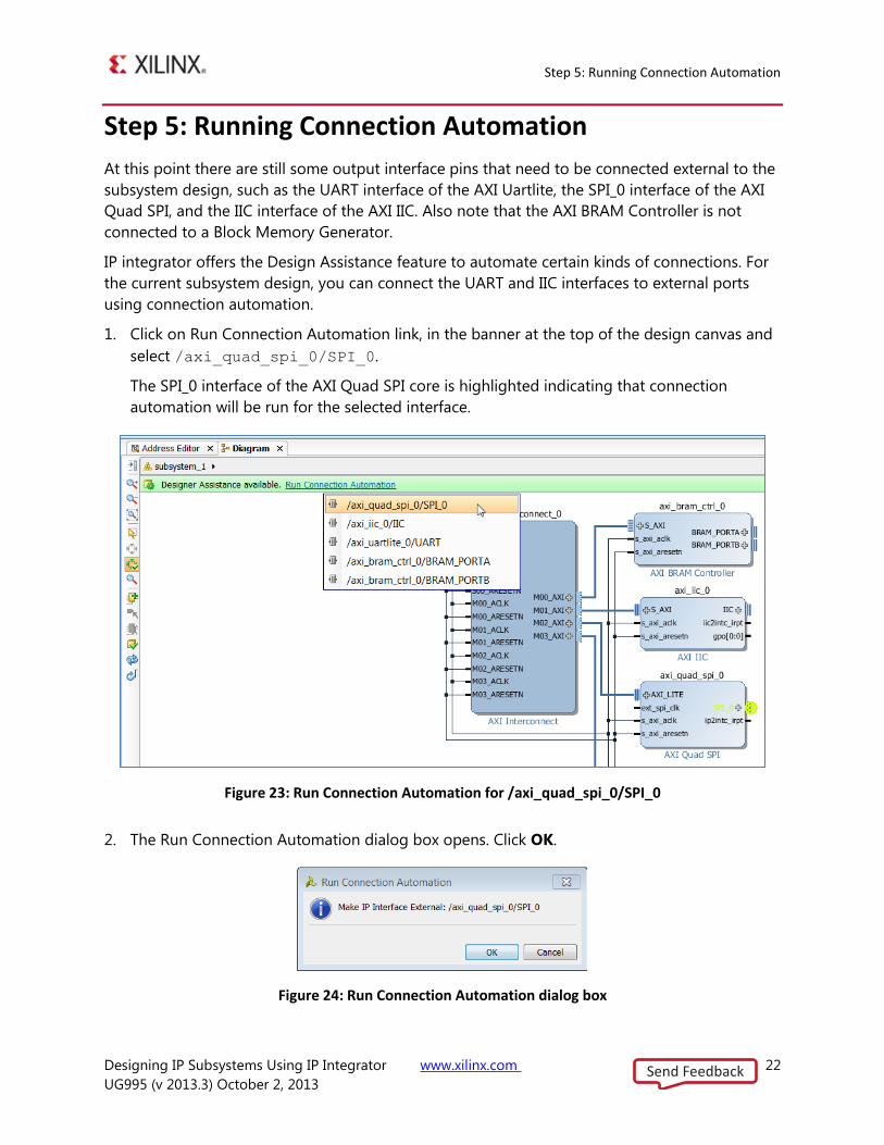
At this point there are still some output interface pins that need to be connected external to the
subsystem design, such as the UART interface of the AXI Uartlite, the SPI_0 interface of the AXI
Quad SPI, and the IIC interface of the AXI IIC. Also note that the AXI BRAM Controller is not
connected to a Block Memory Generator.
IP integrator offers the Design Assistance feature to automate certain kinds of connections. For
the current subsystem design, you can connect the UART and IIC interfaces to external ports
using connection automation.
Click on Run Connection Automation link, in the banner at the top of the design canvas and 1.
select /axi_quad_spi_0/SPI_0.
The SPI_0 interface of the AXI Quad SPI core is highlighted indicating that connection
automation will be run for the selected interface.
Figure 23: Run Connection Automation for /axi_quad_spi_0/SPI_0
The Run Connection Automation dialog box opens. Click OK. 2.
Figure 24: Run Connection Automation dialog box
Send Feedback
Step 5: Running Connection Automation
Designing IP Subsystems Using IP Integrator www.xilinx.com 23
UG995 (v 2013.3) October 2, 2013
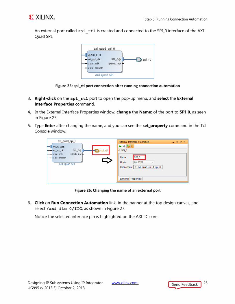
An external port called spi_rtl is created and connected to the SPI_0 interface of the AXI
Quad SPI.
Figure 25: spi_rtl port connection after running connection automation
Right-click on the spi_rtl port to open the pop-up menu, and select the External 3.
Interface Properties command.
In the External Interface Properties window, change the Name: of the port to SPI_0, as seen 4.
in Figure 25.
Type Enter after changing the name, and you can see the set_property command in the Tcl 5.
Console window.
Figure 26: Changing the name of an external port
Click on Run Connection Automation link, in the banner at the top design canvas, and 6.
select /axi_iic_0/IIC, as shown in Figure 27.
Notice the selected interface pin is highlighted on the AXI IIC core.
Send Feedback
Step 5: Running Connection Automation
Designing IP Subsystems Using IP Integrator www.xilinx.com 24
UG995 (v 2013.3) October 2, 2013
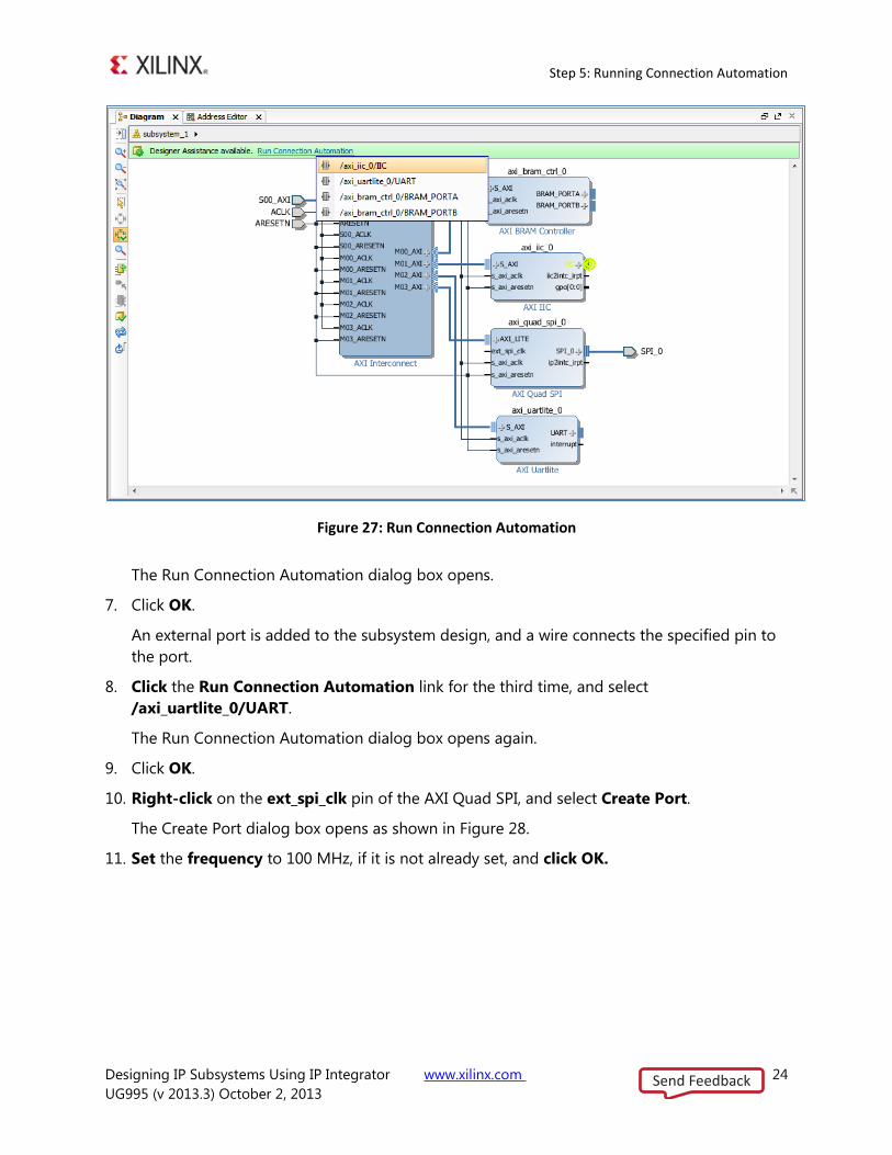
Figure 27: Run Connection Automation
The Run Connection Automation dialog box opens.
Click OK. 7.
An external port is added to the subsystem design, and a wire connects the specified pin to
the port.
Click the Run Connection Automation link for the third time, and select 8.
/axi_uartlite_0/UART.
The Run Connection Automation dialog box opens again.
Click OK. 9.
Right-click on the ext_spi_clk pin of the AXI Quad SPI, and select Create Port. 10.
The Create Port dialog box opens as shown in Figure 28.
Set the frequency to 100 MHz, if it is not already set, and click OK. 11.
Send Feedback
Step 5: Running Connection Automation
Designing IP Subsystems Using IP Integrator www.xilinx.com 25
UG995 (v 2013.3) October 2, 2013
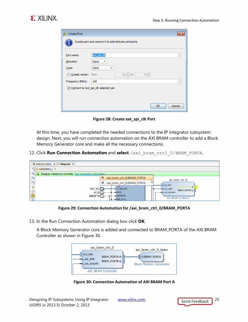
Figure 28: Create ext_spi_clk Port
At this time, you have completed the needed connections to the IP integrator subsystem
design. Next, you will run connection automation on the AXI BRAM controller to add a Block
Memory Generator core and make all the necessary connections.
Click Run Connection Automation and select /axi_bram_ctrl_0/BRAM_PORTA. 12.
Figure 29: Connection Automation for /axi_bram_ctrl_0/BRAM_PORTA
In the Run Connection Automation dialog box click OK. 13.
A Block Memory Generator core is added and connected to BRAM_PORTA of the AXI BRAM
Controller as shown in Figure 30.
Figure 30: Connection Automation of AXI BRAM Port A
Send Feedback
Step 5: Running Connection Automation
Designing IP Subsystems Using IP Integrator www.xilinx.com 26
UG995 (v 2013.3) October 2, 2013
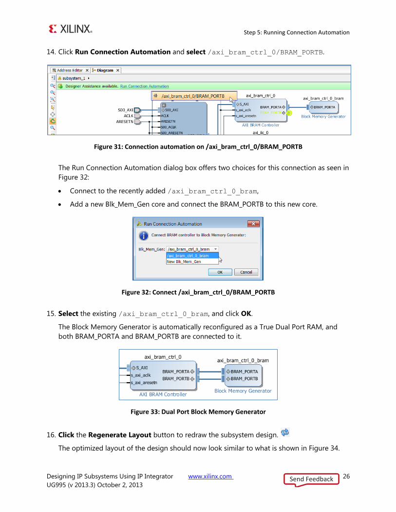
Click Run Connection Automation and select /axi_bram_ctrl_0/BRAM_PORTB. 14.
Figure 31: Connection automation on /axi_bram_ctrl_0/BRAM_PORTB
The Run Connection Automation dialog box offers two choices for this connection as seen in
Figure 32:
Connect to the recently added /axi_bram_ctrl_0_bram,
Add a new Blk_Mem_Gen core and connect the BRAM_PORTB to this new core.
Figure 32: Connect /axi_bram_ctrl_0/BRAM_PORTB
Select the existing /axi_bram_ctrl_0_bram, and click OK. 15.
The Block Memory Generator is automatically reconfigured as a True Dual Port RAM, and
both BRAM_PORTA and BRAM_PORTB are connected to it.
Figure 33: Dual Port Block Memory Generator
Click the Regenerate Layout button to redraw the subsystem design. 16.
The optimized layout of the design should now look similar to what is shown in Figure 34.
Send Feedback
Step 5: Running Connection Automation
Designing IP Subsystems Using IP Integrator www.xilinx.com 27
UG995 (v 2013.3) October 2, 2013
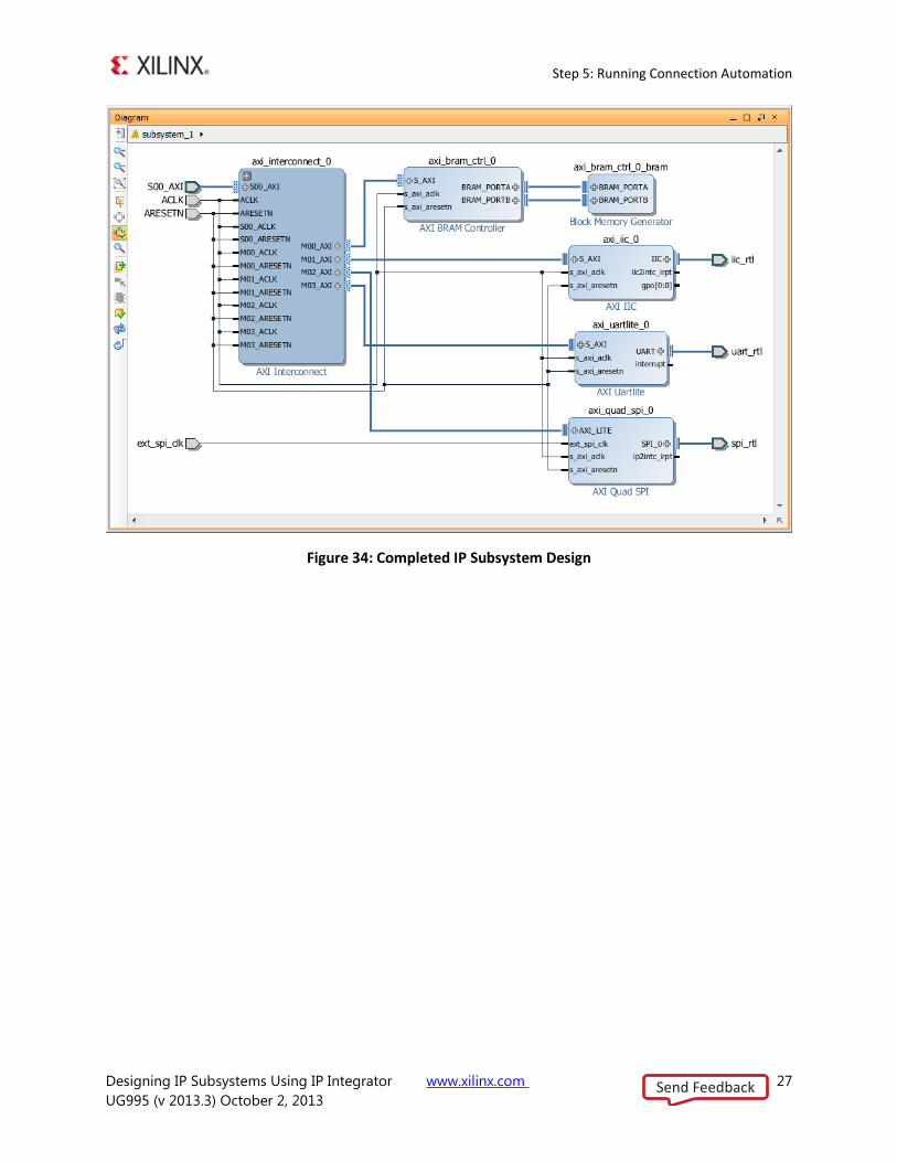
Figure 34: Completed IP Subsystem Design
Send Feedback
Step 6: Using the Address Editor
Designing IP Subsystems Using IP Integrator www.xilinx.com 28
UG995 (v 2013.3) October 2, 2013
Step 6: Using the Address Editor
For various memory mapped master and slave interfaces, IP integrator follows the industry
standard IP-XACT data format for capturing memory requirements and capabilities of endpoint
masters and slaves. This section provides an overview of how IP integrator models address
information on a memory mapped slave.
Master interfaces have address spaces, or address_space objects. Slave interfaces have an
address_space container, called a memory map, to map the slave to the address space of the
associated master. These memory maps are usually named after the slave interface pins, for
example S_AXI, though that is not required.
The memory map for each slave interface pin contains address segments, or address_segment
objects. These address segments correspond to the address decode window for that slave. A
typical AXI4-Lite slave will have only one address segment, representing a range of addresses.
However, some slaves, like a bridge, will have multiple address segments; or a range of
addresses for each address decode window.
When a slave is mapped to the master address space, a master address_segment object is
created, mapping the address segments of the slave to the master. The Vivado IP integrator can
automatically assign addresses for all slaves in the design. However, you can also manually
assign the addresses using the Address Editor. In the Address Editor, you see the address
segments of the slaves, and can map them to address spaces in the masters.
TIP: The Address Editor tab only appears if the subsystem design contains an IP block that
functions as a bus master. In the tutorial design, the external processor connecting through
the AXI Interconnect is the bus master.
Click the Address Editor tab to show the memory map of all the slaves in the design. 1.
Note: If the Address Editor tab is not visible then open it with the Window > Address
Editor command from the main menu.
You can expand the Unmapped Slaves folder by clicking on the ‘+’ sign if necessary.
Figure 35: Address Editor
Send Feedback
Step 6: Using the Address Editor
Designing IP Subsystems Using IP Integrator www.xilinx.com 29
UG995 (v 2013.3) October 2, 2013
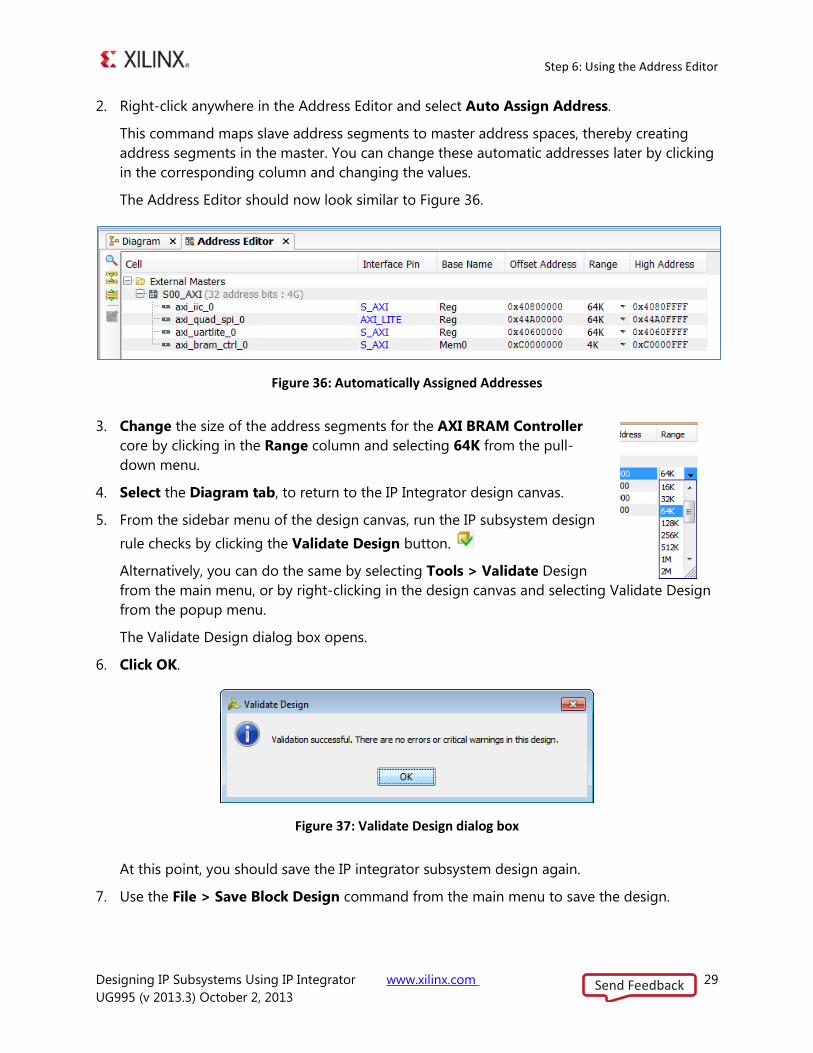
Right-click anywhere in the Address Editor and select Auto Assign Address. 2.
This command maps slave address segments to master address spaces, thereby creating
address segments in the master. You can change these automatic addresses later by clicking
in the corresponding column and changing the values.
The Address Editor should now look similar to Figure 36.
Figure 36: Automatically Assigned Addresses
Change the size of the address segments for the AXI BRAM Controller 3.
core by clicking in the Range column and selecting 64K from the pull-
down menu.
Select the Diagram tab, to return to the IP Integrator design canvas. 4.
From the sidebar menu of the design canvas, run the IP subsystem design 5.
rule checks by clicking the Validate Design button.
Alternatively, you can do the same by selecting Tools > Validate Design
from the main menu, or by right-clicking in the design canvas and selecting Validate Design
from the popup menu.
The Validate Design dialog box opens.
Click OK. 6.
Figure 37: Validate Design dialog box
At this point, you should save the IP integrator subsystem design again.
Use the File > Save Block Design command from the main menu to save the design. 7.
Send Feedback
Step 7: Creating and Implementing the Top-Level Design
Designing IP Subsystems Using IP Integrator www.xilinx.com 30
UG995 (v 2013.3) October 2, 2013
Step 7: Creating and Implementing the Top-Level Design
With the IP subsystem design completed and validated, you need to prepare it for inclusion into
the top-level HDL design. The subsystem can be included as a module or block of the top-level
design, or may be the only block of the top-level design. In either case, you need to generate
the HDL files for the subsystem design.
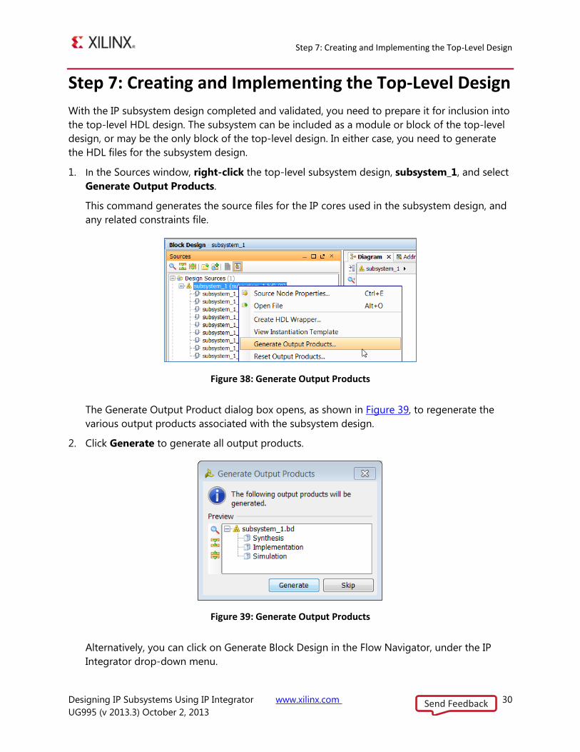
In the Sources window, right-click the top-level subsystem design, subsystem_1, and select 1.
Generate Output Products.
This command generates the source files for the IP cores used in the subsystem design, and
any related constraints file.
Figure 38: Generate Output Products
The Generate Output Product dialog box opens, as shown in Figure 39, to regenerate the
various output products associated with the subsystem design.
Click Generate to generate all output products. 2.
Figure 39: Generate Output Products
Alternatively, you can click on Generate Block Design in the Flow Navigator, under the IP
Integrator drop-down menu.
Send Feedback
Step 7: Creating and Implementing the Top-Level Design
Designing IP Subsystems Using IP Integrator www.xilinx.com 31
UG995 (v 2013.3) October 2, 2013
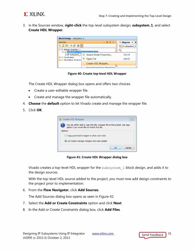
In the Sources window, right-click the top-level subsystem design, subsystem_1, and select 3.
Create HDL Wrapper.
Figure 40: Create top-level HDL Wrapper
The Create HDL Wrapper dialog box opens and offers two choices.
Create a user-editable wrapper file.
Create and manage the wrapper file automatically.
Choose the default option to let Vivado create and manage the wrapper file. 4.
Click OK. 5.
Figure 41: Create HDL Wrapper dialog box
Vivado creates a top-level HDL wrapper for the subsystem_1 block design, and adds it to
the design sources.
With the top-level HDL source added to the project, you must now add design constraints to
the project prior to implementation.
From the Flow Navigator, click Add Sources. 6.
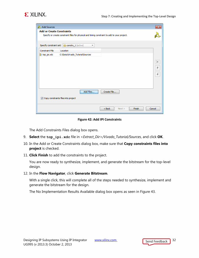
The Add Sources dialog box opens as seen in Figure 42.
Select the Add or Create Constraints option and click Next. 7.
In the Add or Create Constraints dialog box, click Add Files. 8.
Send Feedback
Step 7: Creating and Implementing the Top-Level Design
Designing IP Subsystems Using IP Integrator www.xilinx.com 32
UG995 (v 2013.3) October 2, 2013
Figure 42: Add IPI Constraints
The Add Constraints Files dialog box opens.
Select the top_ipi.xdc file in <Extract_Dir>/Vivado_Tutorial/Sources, and click OK. 9.
In the Add or Create Constraints dialog box, make sure that Copy constraints files into 10.
project is checked.
Click Finish to add the constraints to the project. 11.
You are now ready to synthesize, implement, and generate the bitstream for the top-level
design.
In the Flow Navigator, click Generate Bitstream. 12.
With a single click, this will complete all of the steps needed to synthesize, implement and
generate the bitstream for the design.
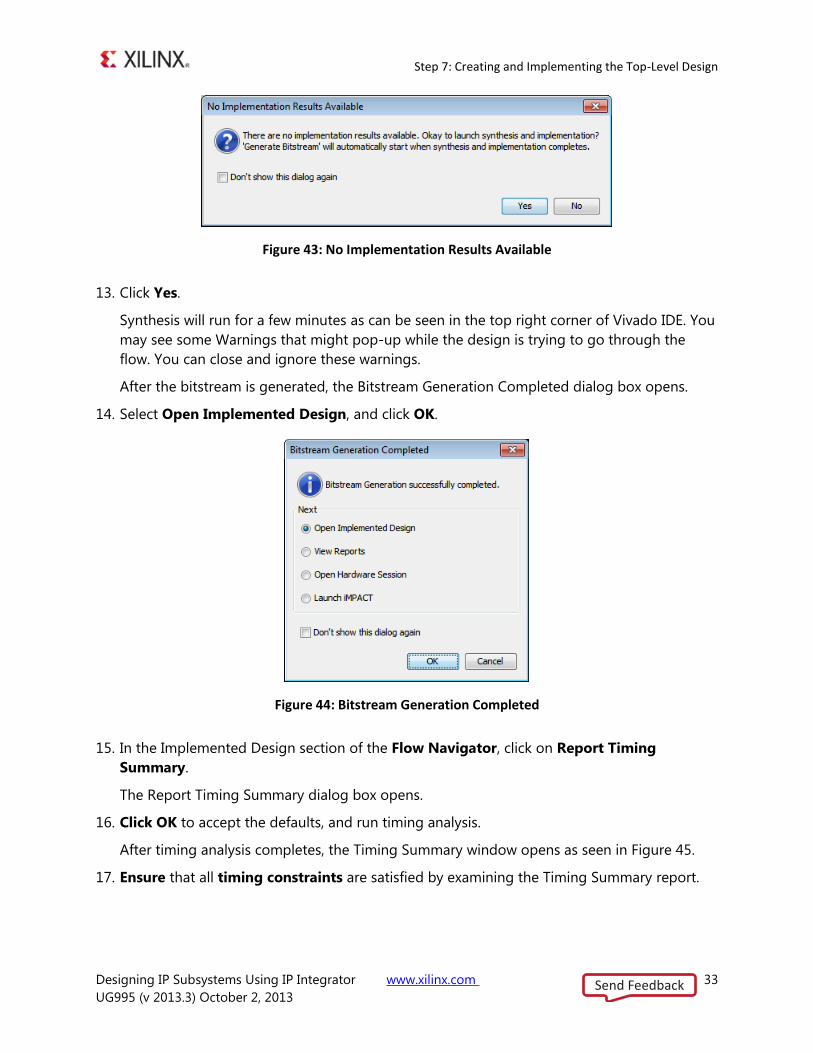
The No Implementation Results Available dialog box opens as seen in Figure 43.
Send Feedback
Step 7: Creating and Implementing the Top-Level Design
Designing IP Subsystems Using IP Integrator www.xilinx.com 33
UG995 (v 2013.3) October 2, 2013
Figure 43: No Implementation Results Available
Click Yes. 13.
Synthesis will run for a few minutes as can be seen in the top right corner of Vivado IDE. You
may see some Warnings that might pop-up while the design is trying to go through the
flow. You can close and ignore these warnings.
After the bitstream is generated, the Bitstream Generation Completed dialog box opens.
Select Open Implemented Design, and click OK. 14.
Figure 44: Bitstream Generation Completed
In the Implemented Design section of the Flow Navigator, click on Report Timing 15.
Summary.
The Report Timing Summary dialog box opens.
Click OK to accept the defaults, and run timing analysis. 16.
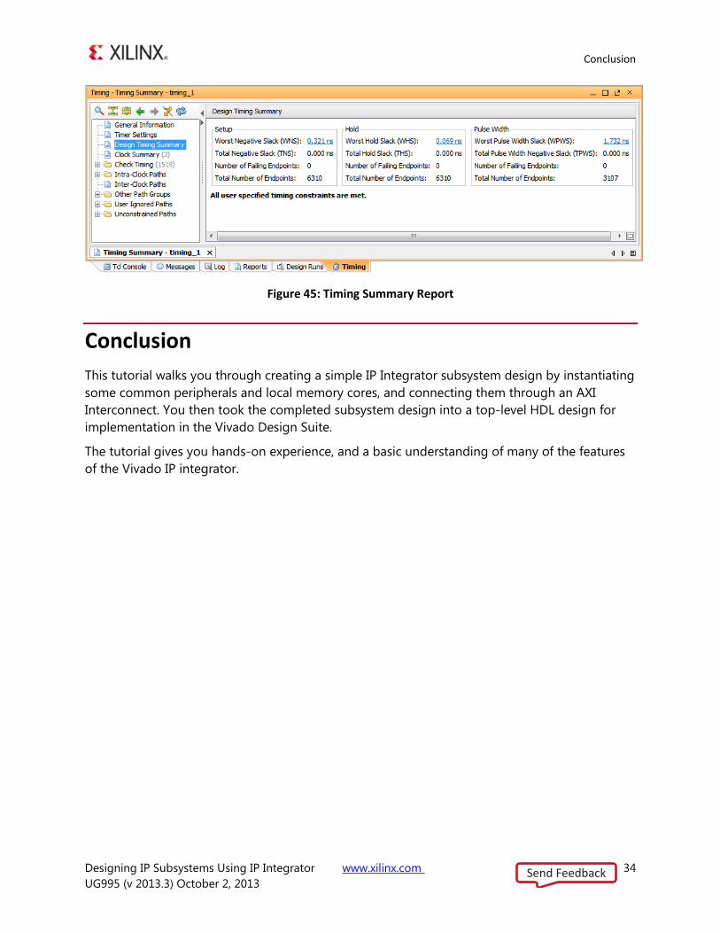
After timing analysis completes, the Timing Summary window opens as seen in Figure 45.
Ensure that all timing constraints are satisfied by examining the Timing Summary report. 17.
Send Feedback
Conclusion
Designing IP Subsystems Using IP Integrator www.xilinx.com 34
UG995 (v 2013.3) October 2, 2013
Figure 45: Timing Summary Report
Conclusion
This tutorial walks you through creating a simple IP Integrator subsystem design by instantiating
some common peripherals and local memory cores, and connecting them through an AXI
Interconnect. You then took the completed subsystem design into a top-level HDL design for
implementation in the Vivado Design Suite.
The tutorial gives you hands-on experience, and a basic understanding of many of the features
of the Vivado IP integrator.
Send Feedback