Embed Size (px)
Citation preview

Vivado Design Suite User Guide
Design Analysis and Closure Techniques
UG906 (v2016.3) October 5, 2016UG906 (v2016.4) November 30, 2016

Design Analysis and Closure Techniques 2UG906 (v2016.3) October 5, 2016 www.xilinx.com
Revision HistoryThe following table shows the revision history for this document.
Date Version Revision
10/05/2016 2016.3 Updated for Vivado® Design Suite 2016.3 release. Updates include:
• Updated figures.
• Added Clock Pair Classification, page 43.
• Added Report Clock Utilization, page 131.
• Added Clock Phase Shift, page 156.
06/08/2016 2016.2 Updated for Vivado Design Suite 2016.2 release. Changes include:
• Chapter 2: Added information to multiple_clock, generated_clocks, and latch_loops checks in Check Timing Section.
• Chapter 6: Restructured and renamed chapter. New content includes:
° Using the Elaborated View to Optimize the RTL (moved from Chapter 7)
° Optimizing RAMB Utilization when Memory Depth is not a Power of 2
° Optimizing RAMB Input Logic to Allow Output Register Inference
° Improving Critical Logic on RAMB Outputs
• Chapter 7: Restructured and renamed chapter. Added Floorplanning (moved from Chapter 6).
• Updated links to the UltraFast Design Methodology Guide for the Vivado Design Suite (UG949).
05/03/2016 2016.1 Updated for Vivado Design Suite 2016.1 release. Changes include:
• Updated figures in chapters 1 and 2.
• Documented report_methodology command in Using Report DRC and Validating Design Methodology DRCs.
• Added information about safe, unsafe, and endpoint terminology in Terminology.
• Added Report Bus Skew.
• Added information about report_bus_skew command in Verifying Timing Signoff.
• Updated description of the create_generated_clock command in TIMING-30: Sub-Optimal Master Source Pin Selection for Generated Clock.
Send FeedbackUG906 (v2016.4) November 30, 2016
11/30/2016: Released with Vivado® Design Suite 2016.4 without changes from 2016.3.

Design Analysis and Closure Techniques 3UG906 (v2016.3) October 5, 2016 www.xilinx.com
Table of ContentsChapter 1: Logic Analysis Within the IDE
Design Analysis Within the IDE . . . . . . . . . . . . . . . . . . . . . . . . . . . . . . . . . . . . . . . . . . . . . . . . . . . . . . . 6Logic Analysis Features . . . . . . . . . . . . . . . . . . . . . . . . . . . . . . . . . . . . . . . . . . . . . . . . . . . . . . . . . . . . . 6Using the Netlist Window . . . . . . . . . . . . . . . . . . . . . . . . . . . . . . . . . . . . . . . . . . . . . . . . . . . . . . . . . . . 7Using the Hierarchy Window . . . . . . . . . . . . . . . . . . . . . . . . . . . . . . . . . . . . . . . . . . . . . . . . . . . . . . . . 9Using the Schematic Window . . . . . . . . . . . . . . . . . . . . . . . . . . . . . . . . . . . . . . . . . . . . . . . . . . . . . . . 10Searching for Objects Using the Find Dialog Box . . . . . . . . . . . . . . . . . . . . . . . . . . . . . . . . . . . . . . . . 14Analyzing Device Utilization Statistics . . . . . . . . . . . . . . . . . . . . . . . . . . . . . . . . . . . . . . . . . . . . . . . . 17Using Report DRC. . . . . . . . . . . . . . . . . . . . . . . . . . . . . . . . . . . . . . . . . . . . . . . . . . . . . . . . . . . . . . . . . 18Validating Design Methodology DRCs . . . . . . . . . . . . . . . . . . . . . . . . . . . . . . . . . . . . . . . . . . . . . . . . 18
Chapter 2: Timing Analysis FeaturesReport Timing Summary . . . . . . . . . . . . . . . . . . . . . . . . . . . . . . . . . . . . . . . . . . . . . . . . . . . . . . . . . . . 20Report Clock Networks . . . . . . . . . . . . . . . . . . . . . . . . . . . . . . . . . . . . . . . . . . . . . . . . . . . . . . . . . . . . 37Report Clock Interaction . . . . . . . . . . . . . . . . . . . . . . . . . . . . . . . . . . . . . . . . . . . . . . . . . . . . . . . . . . . 39Report Pulse Width . . . . . . . . . . . . . . . . . . . . . . . . . . . . . . . . . . . . . . . . . . . . . . . . . . . . . . . . . . . . . . . 47Report Timing. . . . . . . . . . . . . . . . . . . . . . . . . . . . . . . . . . . . . . . . . . . . . . . . . . . . . . . . . . . . . . . . . . . . 47Report Datasheet. . . . . . . . . . . . . . . . . . . . . . . . . . . . . . . . . . . . . . . . . . . . . . . . . . . . . . . . . . . . . . . . . 53Report Exceptions . . . . . . . . . . . . . . . . . . . . . . . . . . . . . . . . . . . . . . . . . . . . . . . . . . . . . . . . . . . . . . . . 60Report Clock Domain Crossings . . . . . . . . . . . . . . . . . . . . . . . . . . . . . . . . . . . . . . . . . . . . . . . . . . . . . 66Report Bus Skew . . . . . . . . . . . . . . . . . . . . . . . . . . . . . . . . . . . . . . . . . . . . . . . . . . . . . . . . . . . . . . . . . 85
Chapter 3: Implementation Results Analysis FeaturesUsing the Design Runs Window . . . . . . . . . . . . . . . . . . . . . . . . . . . . . . . . . . . . . . . . . . . . . . . . . . . . . 89Placement Analysis . . . . . . . . . . . . . . . . . . . . . . . . . . . . . . . . . . . . . . . . . . . . . . . . . . . . . . . . . . . . . . . 91Routing Analysis. . . . . . . . . . . . . . . . . . . . . . . . . . . . . . . . . . . . . . . . . . . . . . . . . . . . . . . . . . . . . . . . . . 98Report Design Analysis . . . . . . . . . . . . . . . . . . . . . . . . . . . . . . . . . . . . . . . . . . . . . . . . . . . . . . . . . . . 101
Chapter 4: Viewing Reports and MessagesIntroduction to Reports and Messages . . . . . . . . . . . . . . . . . . . . . . . . . . . . . . . . . . . . . . . . . . . . . . 124Viewing and Managing Messages in the IDE . . . . . . . . . . . . . . . . . . . . . . . . . . . . . . . . . . . . . . . . . . 125Vivado Generated Reports and Messages . . . . . . . . . . . . . . . . . . . . . . . . . . . . . . . . . . . . . . . . . . . . 128Creating Design Related Reports . . . . . . . . . . . . . . . . . . . . . . . . . . . . . . . . . . . . . . . . . . . . . . . . . . . 129
Send FeedbackUG906 (v2016.4) November 30, 2016

Design Analysis and Closure Techniques 4UG906 (v2016.3) October 5, 2016 www.xilinx.com
Chapter 5: Performing Timing AnalysisIntroduction to Timing Analysis . . . . . . . . . . . . . . . . . . . . . . . . . . . . . . . . . . . . . . . . . . . . . . . . . . . . 148Understanding the Basics of Timing Analysis. . . . . . . . . . . . . . . . . . . . . . . . . . . . . . . . . . . . . . . . . . 152Reading a Timing Path Report. . . . . . . . . . . . . . . . . . . . . . . . . . . . . . . . . . . . . . . . . . . . . . . . . . . . . . 162Verifying Timing Signoff . . . . . . . . . . . . . . . . . . . . . . . . . . . . . . . . . . . . . . . . . . . . . . . . . . . . . . . . . . 171
Chapter 6: Synthesis Analysis and Closure TechniquesUsing the Elaborated View to Optimize the RTL . . . . . . . . . . . . . . . . . . . . . . . . . . . . . . . . . . . . . . . 172Optimizing RAMB Utilization when Memory Depth is not a Power of 2 . . . . . . . . . . . . . . . . . . . . 175Optimizing RAMB Input Logic to Allow Output Register Inference . . . . . . . . . . . . . . . . . . . . . . . . 179Improving Critical Logic on RAMB Outputs . . . . . . . . . . . . . . . . . . . . . . . . . . . . . . . . . . . . . . . . . . . 183
Chapter 7: Implementation Analysis and Closure TechniquesUsing the report_design_analysis Command. . . . . . . . . . . . . . . . . . . . . . . . . . . . . . . . . . . . . . . . . . 187Identifying the Longest Logic Delay Paths in the Design. . . . . . . . . . . . . . . . . . . . . . . . . . . . . . . . . 191Identifying High Fanout Net Drivers . . . . . . . . . . . . . . . . . . . . . . . . . . . . . . . . . . . . . . . . . . . . . . . . . 192Determining if Hold-Fixing is Negatively Impacting the Design . . . . . . . . . . . . . . . . . . . . . . . . . . . 194Quickly Analyzing All Failing Paths . . . . . . . . . . . . . . . . . . . . . . . . . . . . . . . . . . . . . . . . . . . . . . . . . . 196Floorplanning . . . . . . . . . . . . . . . . . . . . . . . . . . . . . . . . . . . . . . . . . . . . . . . . . . . . . . . . . . . . . . . . . . . 197
Appendix A: Timing Methodology ChecksTIMING-1: Invalid Clock Waveform on Clock Modifying Block . . . . . . . . . . . . . . . . . . . . . . . . . . . . 212TIMING-2: Invalid Primary Clock on Internal Pin . . . . . . . . . . . . . . . . . . . . . . . . . . . . . . . . . . . . . . . 214TIMING-3: Invalid Primary Clock on Clock Modifying Block . . . . . . . . . . . . . . . . . . . . . . . . . . . . . . 215TIMING-4: Invalid Primary Clock Redefinition on a Clock Tree. . . . . . . . . . . . . . . . . . . . . . . . . . . . 217TIMING-5: Invalid Waveform Redefinition on a Clock Tree . . . . . . . . . . . . . . . . . . . . . . . . . . . . . . 218TIMING-6: No Common Primary Clock Between Related Clocks . . . . . . . . . . . . . . . . . . . . . . . . . . 219TIMING-7: No Common Node Between Related Clocks . . . . . . . . . . . . . . . . . . . . . . . . . . . . . . . . . 220TIMING-8: No Common Period Between Related Clocks . . . . . . . . . . . . . . . . . . . . . . . . . . . . . . . . 221TIMING-9: Unknown CDC Logic. . . . . . . . . . . . . . . . . . . . . . . . . . . . . . . . . . . . . . . . . . . . . . . . . . . . . 222TIMING-10: Missing Property on Synchronizer . . . . . . . . . . . . . . . . . . . . . . . . . . . . . . . . . . . . . . . . 223TIMING-11: Inappropriate Max Delay with Datapath Only Option . . . . . . . . . . . . . . . . . . . . . . . . 224TIMING-12: Clock Reconvergence Pessimism Removal Disabled . . . . . . . . . . . . . . . . . . . . . . . . . . 225TIMING-13: Timing Paths Ignored Due to Path Segmentation . . . . . . . . . . . . . . . . . . . . . . . . . . . . 225TIMING-14: LUT on the Clock Tree . . . . . . . . . . . . . . . . . . . . . . . . . . . . . . . . . . . . . . . . . . . . . . . . . . 226TIMING-15: Large Hold Violation on Inter-Clock Path. . . . . . . . . . . . . . . . . . . . . . . . . . . . . . . . . . . 227TIMING-16: Large Setup Violation . . . . . . . . . . . . . . . . . . . . . . . . . . . . . . . . . . . . . . . . . . . . . . . . . . 228TIMING-17: Non-Clocked Sequential Cell . . . . . . . . . . . . . . . . . . . . . . . . . . . . . . . . . . . . . . . . . . . . . 229TIMING-18: Missing Input or Output Delay . . . . . . . . . . . . . . . . . . . . . . . . . . . . . . . . . . . . . . . . . . . 229TIMING-19: Inverted Generated Clock Waveform on ODDR . . . . . . . . . . . . . . . . . . . . . . . . . . . . . 230
Send FeedbackUG906 (v2016.4) November 30, 2016
Design Analysis and Closure Techniques 5UG906 (v2016.3) October 5, 2016 www.xilinx.com
TIMING-20: Non-Clocked Latch. . . . . . . . . . . . . . . . . . . . . . . . . . . . . . . . . . . . . . . . . . . . . . . . . . . . . 230TIMING-21: Invalid COMPENSATION Property on MMCM . . . . . . . . . . . . . . . . . . . . . . . . . . . . . . . 231TIMING-22: Missing External Delay on MMCM . . . . . . . . . . . . . . . . . . . . . . . . . . . . . . . . . . . . . . . . 232TIMING-23: Combinatorial Loop Found . . . . . . . . . . . . . . . . . . . . . . . . . . . . . . . . . . . . . . . . . . . . . . 233TIMING-24: Overridden Max Delay Datapath Only . . . . . . . . . . . . . . . . . . . . . . . . . . . . . . . . . . . . . 233TIMING-25: Invalid Clock Waveform on Gigabit Transceiver (GT) . . . . . . . . . . . . . . . . . . . . . . . . . 234TIMING-26: Missing Clock on Gigabit Transceiver (GT). . . . . . . . . . . . . . . . . . . . . . . . . . . . . . . . . . 235TIMING-27: Invalid Primary Clock on Hierarchical Pin . . . . . . . . . . . . . . . . . . . . . . . . . . . . . . . . . . 235TIMING-28: Auto-Derived Clock Referenced by a Timing Constraint. . . . . . . . . . . . . . . . . . . . . . . 236TIMING-29: Inconsistent Pair of Multicycle Paths . . . . . . . . . . . . . . . . . . . . . . . . . . . . . . . . . . . . . . 237TIMING-30: Sub-Optimal Master Source Pin Selection for Generated Clock. . . . . . . . . . . . . . . . . 238
Appendix B: Additional Resources and Legal NoticesXilinx Resources . . . . . . . . . . . . . . . . . . . . . . . . . . . . . . . . . . . . . . . . . . . . . . . . . . . . . . . . . . . . . . . . . 239Solution Centers. . . . . . . . . . . . . . . . . . . . . . . . . . . . . . . . . . . . . . . . . . . . . . . . . . . . . . . . . . . . . . . . . 239Documentation Navigator and Design Hubs . . . . . . . . . . . . . . . . . . . . . . . . . . . . . . . . . . . . . . . . . . 239References . . . . . . . . . . . . . . . . . . . . . . . . . . . . . . . . . . . . . . . . . . . . . . . . . . . . . . . . . . . . . . . . . . . . . 240Training Resources. . . . . . . . . . . . . . . . . . . . . . . . . . . . . . . . . . . . . . . . . . . . . . . . . . . . . . . . . . . . . . . 240Please Read: Important Legal Notices . . . . . . . . . . . . . . . . . . . . . . . . . . . . . . . . . . . . . . . . . . . . . . . 241
Send FeedbackUG906 (v2016.4) November 30, 2016
Design Analysis and Closure Techniques 6UG906 (v2016.3) October 5, 2016 www.xilinx.com
Chapter 1
Logic Analysis Within the IDE
Design Analysis Within the IDEThe following chapters provide an introduction to design analysis in the Xilinx® Vivado® Design Suite Integrated Design Environment (IDE):
• Logic Analysis Within the IDE (this chapter)
• Chapter 2, Timing Analysis Features
• Chapter 3, Implementation Results Analysis Features
Logic Analysis FeaturesThis chapter discusses Logic Analysis Features, and includes:
• Using the Netlist Window
• Using the Hierarchy Window
• Using the Schematic Window
• Searching for Objects Using the Find Dialog Box
• Analyzing Device Utilization Statistics
• Using Report DRC
• Validating Design Methodology DRCs
Send FeedbackUG906 (v2016.4) November 30, 2016

Design Analysis and Closure Techniques 7UG906 (v2016.3) October 5, 2016 www.xilinx.com
Chapter 1: Logic Analysis Within the IDE
Using the Netlist WindowThe Netlist Window shows the design hierarchy as it is in the netlist, processed by the synthesis tools.
Depending on synthesis settings, the netlist hierarchy may be a one hundred percent match for the original RTL, or there may be no hierarchy. Generally, the synthesis tools default to preserving most of the user hierarchy while optimizing the logic. This results in a smaller, faster netlist.
With the synthesis tool defaults, the netlist hierarchy is recognizable, but the interfaces to the hierarchies may be modified. Some pins and levels of hierarchy may be missing.
Each level of hierarchy shows its hierarchy tree. At each level, the tool shows:
• A nets folder for any nets at that level
• A Leaf Cells folder if there are hardware primitive instances at that level
• Any hierarchies instantiated at that level
Traversing the tree shows the whole branch. The icons next to the cells display information about the state of the design.
X-Ref Target - Figure 1-1
Figure 1-1: Netlist Window
Send FeedbackUG906 (v2016.4) November 30, 2016

Design Analysis and Closure Techniques 8UG906 (v2016.3) October 5, 2016 www.xilinx.com
Chapter 1: Logic Analysis Within the IDE
For more information, see this link in the Vivado Design Suite User Guide: Using the Vivado IDE (UG893) [Ref 1].
The Properties Window for each level of hierarchy shows utilization statistics including:
• Primitive usage for the whole hierarchical branch, grouped in higher level buckets
• The number of nets crossing the hierarchy boundary
• Clocks used in the hierarchy
If you floorplan the design, similar properties are displayed for the Pblock.
X-Ref Target - Figure 1-2
Figure 1-2: Instance Properties Window
Send FeedbackUG906 (v2016.4) November 30, 2016

Design Analysis and Closure Techniques 9UG906 (v2016.3) October 5, 2016 www.xilinx.com
Chapter 1: Logic Analysis Within the IDE
Using the Hierarchy WindowExplore the hierarchy to understand resource usage. To open the Hierarchy Window, select Tools > Show Hierarchy, or from the Netlist window, click F6.
As shown in the following figure, the Hierarchy Window displays the hierarchy tree for the netlist. Each horizontal row displays a level of hierarchy inside the netlist. As you move down the rows, you move into deeper netlist hierarchy. Across the row, each level of hierarchy is sized relative to the other hierarchy at that level.
Figure 1-3 shows that cpuEngine, usbEngine0, and usbEngine1 have most of the logic in the design, and all use about the same number of resources.
The Utilization Report breaks apart the design based on resource type. It displays each resource type independently with consumption per level of hierarchy.
To view the Utilization Report, select Tools > Report > Report Utilization. Figure 1-4 shows the Utilization Report.
X-Ref Target - Figure 1-3
Figure 1-3: Hierarchy Window
Send FeedbackUG906 (v2016.4) November 30, 2016

Design Analysis and Closure Techniques 10UG906 (v2016.3) October 5, 2016 www.xilinx.com
Chapter 1: Logic Analysis Within the IDE
In this design, the two usbEngine blocks are the two biggest consumers of the RAMB36 and FIFO36 blocks. Click the + (plus) icon to view the consumption at sub-hierarchies.
Using the Schematic WindowThe schematic is a graphical representation of the netlist. View the schematic to:
• View a graphical representation for the netlist.
• Review the gates, hierarchies, and connectivity.
• Trace and expand cones of logic.
• Analyze the design.
• Better understand what is happening inside the design.
X-Ref Target - Figure 1-4
Figure 1-4: Utilization Report
Send FeedbackUG906 (v2016.4) November 30, 2016

Design Analysis and Closure Techniques 11UG906 (v2016.3) October 5, 2016 www.xilinx.com
Chapter 1: Logic Analysis Within the IDE
At the RTL level in Elaborated Design, you see how the tool has interpreted your code. In Synthesize Design and Implemented Design, you see the gates generated by the synthesis tool.
To open the schematic, select Tools > Schematic. If nothing is selected, the gates, hierarchy, and connectivity appear at the top level of the design, as shown in Figure 1-5.
For information about zooming and moving around the schematic, see this link in the Vivado Design Suite User Guide: Using the Vivado IDE (UG893) [Ref 1].
TIP: The schematic is simpler if you use a single level of hierarchy only. The schematic populates with the selected element emphasized (blue). The ports for the single hierarchy display.
X-Ref Target - Figure 1-5
Figure 1-5: Top Level Schematic
Send FeedbackUG906 (v2016.4) November 30, 2016

Design Analysis and Closure Techniques 12UG906 (v2016.3) October 5, 2016 www.xilinx.com
Chapter 1: Logic Analysis Within the IDE
You can trace the schematic in multiple ways:
• Click the + (plus) icon in the upper left to display the gates in the hierarchy.
• Double-click a port or element to expand it.
• Use the schematic popup.
For more information about schematics, see this link in the Vivado Design Suite User Guide: Using the Vivado IDE (UG893) [Ref 1].
• Click the <- -> arrows to switch between the previous and next schematic views.
• Select Expand All to display more logic and connectivity.
• Select Collapse All to simplify the schematic.
After implementation, the schematic is the easiest way to visualize the gates in a timing path. Select the path, then open the schematic with the gates and nets from that path.
X-Ref Target - Figure 1-6
Figure 1-6: Schematic with Single Hierarchy Selected
Send FeedbackUG906 (v2016.4) November 30, 2016

Design Analysis and Closure Techniques 13UG906 (v2016.3) October 5, 2016 www.xilinx.com
Chapter 1: Logic Analysis Within the IDE
To identify the relevant levels of hierarchy in the schematic, choose Select Leaf Cell Parents from the popup menu.
X-Ref Target - Figure 1-7
Figure 1-7: Schematic with Timing Path
X-Ref Target - Figure 1-8
Figure 1-8: Timing Path with Select Primitive Parents
Send FeedbackUG906 (v2016.4) November 30, 2016

Design Analysis and Closure Techniques 14UG906 (v2016.3) October 5, 2016 www.xilinx.com
Chapter 1: Logic Analysis Within the IDE
As you review the schematic, select the Highlight and Mark commands to track gates of interest. Color coding primitives (using either a mark or a highlight) makes it easier to track which logic was in the original path, and which logic was added.
Searching for Objects Using the Find Dialog BoxThe Vivado IDE includes powerful find and search capabilities. To open the Find dialog box, select Edit > Find. (See the following figure.)
Note: You can also open the Find window by pressing Ctrl+F.
X-Ref Target - Figure 1-9
Figure 1-9: Schematic with Timing Path Marked
Send FeedbackUG906 (v2016.4) November 30, 2016

Design Analysis and Closure Techniques 15UG906 (v2016.3) October 5, 2016 www.xilinx.com
Chapter 1: Logic Analysis Within the IDE
Find CriteriaThe Find dialog box allows you to search the netlist for a wide range of criteria and properties, as shown in the following figures.
X-Ref Target - Figure 1-10
Figure 1-10: Find Dialog Box
X-Ref Target - Figure 1-11
Figure 1-11: Find Dialog Box Displaying Search Criteria
Send FeedbackUG906 (v2016.4) November 30, 2016

Design Analysis and Closure Techniques 16UG906 (v2016.3) October 5, 2016 www.xilinx.com
Chapter 1: Logic Analysis Within the IDE
Find ExamplesSelect Edit > Find to find, for example:
• All unplaced I/Os
• Only the tool-placed Global Clocks
• All nets with a fanout over 10,000
• All DSPs using the PREG embedded register
Complex FindsTo run a complex find:
1. Set the first search criterion.
2. Click +(plus) next to the Properties drop-down options.
3. Add additional criteria.
4. Join the additional criteria with logical operators (AND, OR).
X-Ref Target - Figure 1-12
Figure 1-12: Find Dialog Box Showing Properties Options
Send FeedbackUG906 (v2016.4) November 30, 2016

Design Analysis and Closure Techniques 17UG906 (v2016.3) October 5, 2016 www.xilinx.com
Chapter 1: Logic Analysis Within the IDE
Tcl FindsFrom the script or Tcl console, use the equivalent Tcl get_* command (such as get_cells) to query Vivado objects.
TIP: The Tcl Console at the bottom of the Vivado IDE shows the Vivado Design Suite Tcl commands run for each action executed in the GUI. From the Tcl Console, you can also enter Vivado Design Suite Tcl commands.
For more information on Tcl scripting, see the Vivado Design Suite User Guide: Using Tcl Scripting (UG894) [Ref 2].
For more information on Tcl commands, see the Vivado Design Suite Tcl Command Reference Guide (UG835) [Ref 3], or type <command> -help.
Analyzing Device Utilization StatisticsA common cause of implementation issues comes from not considering the logic and device layout implied by the pinout. Slice logic is uniform in most devices. However, specialized resources such as the following impact logic placement:
• I/O
• High Performance Banks
• High Range Banks
• MGT
• DSP48
• Block RAM
• MMCM
• BUFG
• BUFR
Blocks that are large consumers of a certain specialized resource may have to spread around the device. Take this into account when designing the interface with the rest of the design. Use a combination of the following to find block resources:
• report_utilization
• netlist properties
• Pblock properties
Send FeedbackUG906 (v2016.4) November 30, 2016

Design Analysis and Closure Techniques 18UG906 (v2016.3) October 5, 2016 www.xilinx.com
Chapter 1: Logic Analysis Within the IDE
Using Report DRCDesign Rule Checks (DRCs) check the design and report on common issues. Since the 2016.1 release, DRCs are split into two different commands. The methodology DRCs have been moved to the report_methodology command, while all other DRCs are in the report_drc command. Run non-methodology DRCs using the report_drc command. During implementation, the tools also run DRCS. The DRCs become more complete and comprehensive with placement and routing.
RECOMMENDED: Review the DRC messages, Critical Warnings, and Warnings early in the flow to prevent issues later.
At Synthesized Design, the optional Report DRC step reports a Critical Warning for the unconstrained I/Os. The routed design DRC report reports the Critical Warnings. You must review the report. At write_bitstream, the DRC has been elevated to an Error. Review the DRC reports early to identify areas of the design that need modification.
Validating Design Methodology DRCsDue to the importance of methodology, the Vivado tools provide the report_methodology command, which specifically checks for compliance with methodology DRCs. There are different types of DRCs depending on the stage of the design process. RTL lint-style checks are run on the elaborated RTL design; netlist-based logic and constraint checks are run on the synthesized design; and implementation and timing checks are run on the implemented design.
X-Ref Target - Figure 1-13
Figure 1-13: Showing Critical Warnings and Error
Send FeedbackUG906 (v2016.4) November 30, 2016

Design Analysis and Closure Techniques 19UG906 (v2016.3) October 5, 2016 www.xilinx.com
Chapter 1: Logic Analysis Within the IDE
To run these checks at the Tcl prompt, open the design to be validated and enter following Tcl command:
report_methodology
To run these checks from the IDE, open the design to be validated and run the Report Methodology command. The dialog box appears, as shown in Figure 1-14.
Violations (if there are any) are listed in the DRC window, as shown in the following figure.
For more information on running design methodology DRCs, refer to this link in the Vivado Design Suite User Guide: System-Level Design Entry (UG895) [Ref 4].
X-Ref Target - Figure 1-14
Figure 1-14: Report Methodology Dialog Box
X-Ref Target - Figure 1-15
Figure 1-15: DRC Violations
Send FeedbackUG906 (v2016.4) November 30, 2016

Design Analysis and Closure Techniques 20UG906 (v2016.3) October 5, 2016 www.xilinx.com
Chapter 2
Timing Analysis Features
Report Timing SummaryTiming analysis is available anywhere in the flow after synthesis. You can review the Timing Summary report files automatically created by the Synthesis and Implementation runs.
If your synthesized or implemented design is loaded in memory, you can also generate an interactive Timing Summary report from:
• Flow Navigator > Synthesis
• Flow Navigator > Implementation
• Tools > Timing > Report Timing Summary
Equivalent Tcl command: report_timing_summary
For more information on the report_timing_summary options, see this link in the Vivado Design Suite Tcl Command Reference Guide (UG835) [Ref 3].
In a synthesized design, the Vivado® IDE timing engine estimates the net delays based on connectivity and fanout. The accuracy of the delays is greater for nets between cells that are already placed by the user. There can be larger clock skew on paths where some of the cells have been pre-placed, such as I/Os and GTs.
In an Implemented Design, the net delays are based on the actual routing information. You must use the Timing Summary report for timing signoff if the design is completely routed. To verify that the design is completely routed, view the Route Status report.
Report Timing Summary Dialog BoxIn the Vivado IDE, the Report Timing Summary dialog box includes the following tabs:
• Options Tab
• Advanced Tab
• Timer Settings Tab
Send FeedbackUG906 (v2016.4) November 30, 2016

Design Analysis and Closure Techniques 21UG906 (v2016.3) October 5, 2016 www.xilinx.com
Chapter 2: Timing Analysis Features
The Results name field at the top of the Report Timing Summary dialog box specifies the name of the graphical report that opens in the Results window. The graphical version of the report includes hyperlinks that allow you to cross-reference nets and cells from the report to Device and Schematic windows, and design source files.
If this field is left empty, the report is returned to the Tcl Console, and a graphical version of the report is not opened in the Results window.
Equivalent Tcl option: -name
Options Tab
The Options tab in the Report Timing Summary dialog box is shown in the figure below.
X-Ref Target - Figure 2-1
Figure 2-1: Report Timing Summary Dialog Box: Options Tab
Send FeedbackUG906 (v2016.4) November 30, 2016

Design Analysis and Closure Techniques 22UG906 (v2016.3) October 5, 2016 www.xilinx.com
Chapter 2: Timing Analysis Features
Report Section
The Report section of the Options tab of the Report Timing Summary dialog box includes:
• Path delay type
Sets the type of analysis to be run. For synthesized designs, only max delay analysis (setup/recovery) is performed by default. For implemented design, both min and max delay analysis (setup/hold, recover/removal) are performed by default. To run min delay analysis only (hold and removal), select delay type min.
Equivalent Tcl option: -delay_type
• Report unconstrained paths
Generates information on paths that do not have timing requirements. This option is checked by default in the Vivado IDE, but is not turned on by default in the equivalent Tcl command report_timing_summary.
Equivalent Tcl option: -report_unconstrained
• Report datasheet
Generates the design datasheet as defined in Report Datasheet, in this chapter.
Equivalent Tcl option: -datasheet
Path Limits Section
The Path Limits section of the Options tab of the Report Timing Summary dialog box includes:
• Maximum number of paths per clock or path group: Controls the maximum number of paths reported per clock pair or path group.
Equivalent Tcl option: -max_paths
• Maximum number of worst paths per endpoint: Controls the maximum number of paths potentially reported per path endpoint. This limit is bounded by the maximum number of paths per clock pair or path group. Therefore, the total number of reported paths is still limited by the number of -max_paths.
Equivalent Tcl option: -nworst
Send FeedbackUG906 (v2016.4) November 30, 2016

Design Analysis and Closure Techniques 23UG906 (v2016.3) October 5, 2016 www.xilinx.com
Chapter 2: Timing Analysis Features
Path Display Section
The Path Display section of the Options tab of the Report Timing Summary dialog box includes:
• Display paths with slack less than: Filters the reported paths based on their slack value. This option does not affect the content of the summary tables.
Equivalent Tcl option: -slack_lesser_than
• Significant digits: Controls the accuracy of the numbers displayed in the report.
Equivalent Tcl option: -significant_digits
Common Section
The following controls common to all three tabs are located at the bottom of the Report Timing Summary dialog box:
• Command: Displays the Tcl command line equivalent of the various options specified in the Report Timing Summary dialog box.
• Open in a New Tab: Opens the results in a new tab, or to replace the last tab opened by the Results window.
• Open in Timing Analysis Layout: Resets the current view layout to the Timing Analysis view layout.
For more information on view layouts, see this link in the Vivado Design Suite User Guide: Using the Vivado IDE (UG893) [Ref 1].
Send FeedbackUG906 (v2016.4) November 30, 2016

Design Analysis and Closure Techniques 24UG906 (v2016.3) October 5, 2016 www.xilinx.com
Chapter 2: Timing Analysis Features
Advanced Tab
The Advanced tab in the Report Timing Summary dialog box is shown in the figure below.
Report Section
• Report from cell: Enable to limit the timing reporting on the particular cell of the design. Only paths that start, end, or are fully contained inside the cell will be reported.
Equivalent Tcl option: -cell
• Show input pins in path: Displays which input pin of the cell is used for the path.
Equivalent Tcl option: -input_pins
RECOMMENDED: Keep this option selected to provide more information about all pins used in the path.
• Report unique Pins: show only one timing path for each unique set of pins.
Equivalent Tcl option: -unique_pins
X-Ref Target - Figure 2-2
Figure 2-2: Report Timing Summary Dialog Box: Advanced Tab
Send FeedbackUG906 (v2016.4) November 30, 2016
Design Analysis and Closure Techniques 25UG906 (v2016.3) October 5, 2016 www.xilinx.com
Chapter 2: Timing Analysis Features
File Output Section
• Write results to file: Writes the result to the specified file name. By default the report is written to the Timing window in the Vivado IDE.
Equivalent Tcl option: -file
• Overwrite/Append: When the report is written to a file, determines whether (1) the specified file is overwritten, or (2) new information is appended to an existing report.
Equivalent Tcl option: -append
Miscellaneous Section
• Ignore command errors: Executes the command quietly, ignoring any command line errors and returning no messages. The command also returns TCL_OK regardless of any errors encountered during execution.
Equivalent Tcl option: -quiet
• Suspend message limits during command execution: Temporarily overrides any message limits and return all messages.
Equivalent Tcl option: -verbose
Timer Settings Tab
To set the timer settings, use either: (1) one of the Vivado IDE timing analysis dialog boxes; or, (2) one of the Tcl commands listed in this section. These settings affect other timing-related commands run in the same Vivado IDE session, except the synthesis and implementation commands.
The timer settings are not saved as a tool preference. The default values are restored for each new session. Do not change the default values. Keeping the default values provides maximum timing analysis coverage with the most accurate delay values.
The Timer Settings tab in the Report Timing Summary dialog box is shown in the figure below.
Send FeedbackUG906 (v2016.4) November 30, 2016

Design Analysis and Closure Techniques 26UG906 (v2016.3) October 5, 2016 www.xilinx.com
Chapter 2: Timing Analysis Features
Interconnect Setting
Controls whether net delays are calculated based on the estimated route distance between leaf cell pins, by the actual routed net, or excludes net delay from timing analysis. This option is automatically set to Estimated for post-synthesis designs, and to Actual for post-implementation designs.
° Estimated: For unplaced cells, the net delay value corresponds to the delay of the best possible placement, based on the nature of the driver and loads as well as the fanout. A net between unplaced leaf cell pins is labeled unplaced in the timing path report.
For placed cells, the net delay depends on the distance between the driver and the load as well as the fanout. This net is labeled estimated in the timing path report.
° Actual: For routed nets, the net delay corresponds to the actual hardware delay of the routed interconnect. This net is labeled routed in the timing path report.
° None: Interconnect delays are not considered in the timing report and net delays are forced to zero.
Equivalent Tcl command: set_delay_model
X-Ref Target - Figure 2-3
Figure 2-3: Report Timing Summary Dialog Box: Timer Settings Tab
Send FeedbackUG906 (v2016.4) November 30, 2016

Design Analysis and Closure Techniques 27UG906 (v2016.3) October 5, 2016 www.xilinx.com
Chapter 2: Timing Analysis Features
Speed Grade Setting
Sets the device speed grade. By default, this option is set based on the part selected when creating a project or opening a design checkpoint. You can change this option to report timing on the same design database against another speed grade without rerunning the complete implementation flow.
Equivalent Tcl command: set_speed_grade
Multi-Corner Configuration Setting
Specifies the type of path delays to be analyzed for the specified timing corner. Valid values are none, max, min, and min_max. Select none to disable timing analysis for the specified corner.
RECOMMENDED: Keep both setup (max) and hold (min) analysis selected for both corners.
Equivalent Tcl command: config_timing_corners
Disable Flight Delays Section
Do not add package delays to I/O delay calculations.
Equivalent Tcl command: config_timing_analysis
Details of the Timing Summary ReportThe Timing Summary Report contains the following sections:
• General Information Section
• Timer Settings Section
• Design Timing Summary Section
• Clock Summary Section
• Check Timing Section
• Intra-Clock Paths Section
• Inter-Clock Paths Section
• Path Groups Section
• User-Ignored Paths Section
• Unconstrained Paths Section
The comprehensive information contained in the Timing Summary Report is similar to the information provided by several reports available from the Vivado IDE (Report Clock Interaction, Report Pulse Width, Report Timing, Check Timing) and to some of the reports available in Tcl only (report_clocks).
Send FeedbackUG906 (v2016.4) November 30, 2016
Design Analysis and Closure Techniques 28UG906 (v2016.3) October 5, 2016 www.xilinx.com
Chapter 2: Timing Analysis Features
However, the Report Timing Summary also includes information that is unique to this report, such as Unconstrained Paths.
General Information Section
The General Information section of the Timing Summary Report provides information about the following:
• Design name
• Selected device, package, and speed grade (with the speed file version)
• Vivado Design Suite release
• Current date
• Equivalent Tcl commands executed to generate the report
Timer Settings Section
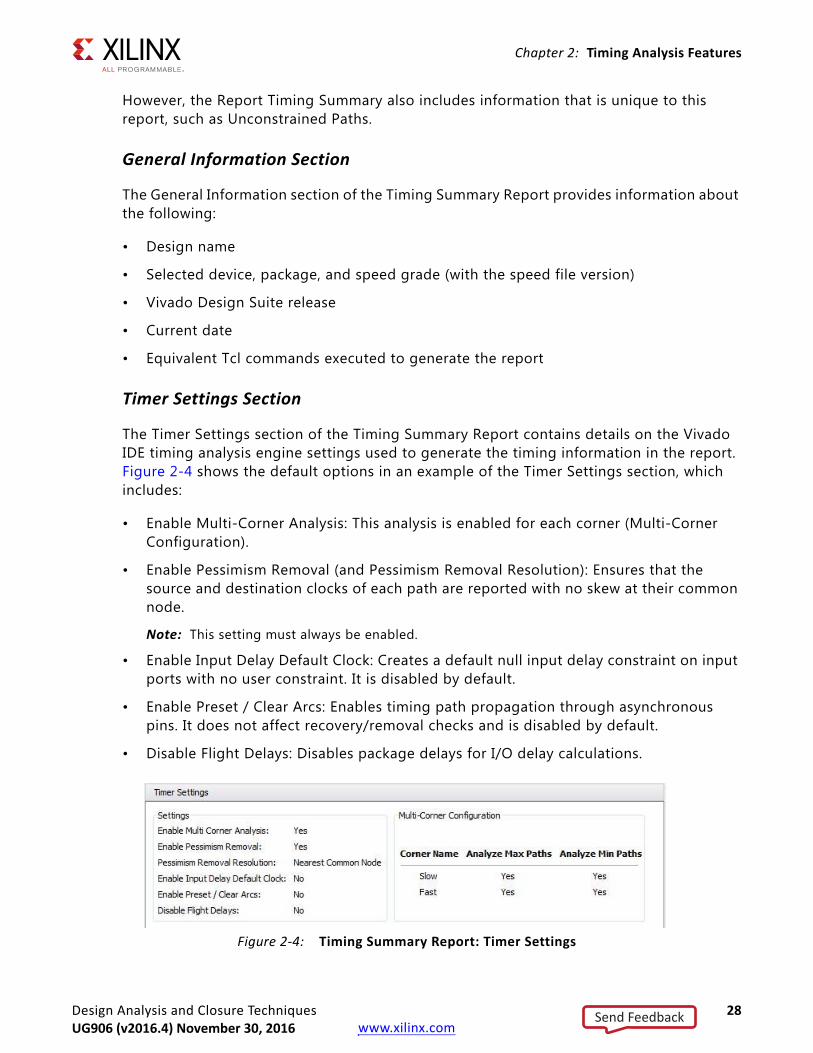
The Timer Settings section of the Timing Summary Report contains details on the Vivado IDE timing analysis engine settings used to generate the timing information in the report. Figure 2-4 shows the default options in an example of the Timer Settings section, which includes:
• Enable Multi-Corner Analysis: This analysis is enabled for each corner (Multi-Corner Configuration).
• Enable Pessimism Removal (and Pessimism Removal Resolution): Ensures that the source and destination clocks of each path are reported with no skew at their common node.
Note: This setting must always be enabled.
• Enable Input Delay Default Clock: Creates a default null input delay constraint on input ports with no user constraint. It is disabled by default.
• Enable Preset / Clear Arcs: Enables timing path propagation through asynchronous pins. It does not affect recovery/removal checks and is disabled by default.
• Disable Flight Delays: Disables package delays for I/O delay calculations.X-Ref Target - Figure 2-4
Figure 2-4: Timing Summary Report: Timer Settings
Send FeedbackUG906 (v2016.4) November 30, 2016

Design Analysis and Closure Techniques 29UG906 (v2016.3) October 5, 2016 www.xilinx.com
Chapter 2: Timing Analysis Features
For additional information on default timer settings and how to change them, see config_timing_analysis, available from this link in the Vivado Design Suite Tcl Command Reference Guide (UG835) [Ref 3].
Design Timing Summary Section
The Design Timing Summary section of the Timing Summary Report (shown in Figure 2-5) provides a summary of the timing for the design, and combines the results of all other sections in one view.
RECOMMENDED: Review the Design Timing Summary section to verify that all timing constraints are met after route, or to understand the status of the design at any point in the flow.
The Design Timing Summary section includes the following:
• Setup Area (Max Delay Analysis)
• Hold Area (Min Delay Analysis)
• Pulse Width Area (Pin Switching Limits)
Setup Area (Max Delay Analysis)
The Setup area of the Design Timing Summary section displays all checks related to max delay analysis: setup, recovery, and data check.
• Worst Negative Slack (WNS): This value corresponds to the worst slack of all the timing paths for max delay analysis. It can be positive or negative.
• Total Negative Slack (TNS): The sum of all WNS violations, when considering only the worst violation of each timing path endpoint. Its value is:
° 0 ns when all timing constraints are met for max delay analysis.
° Negative when there are some violations.
• Number of Failing Endpoints: The total number of endpoints with a violation (WNS<0 ns).
• Total Number of Endpoints: The total number of endpoints analyzed.
X-Ref Target - Figure 2-5
Figure 2-5: Design Timing Summary
Send FeedbackUG906 (v2016.4) November 30, 2016

Design Analysis and Closure Techniques 30UG906 (v2016.3) October 5, 2016 www.xilinx.com
Chapter 2: Timing Analysis Features
Hold Area (Min Delay Analysis)
The Hold area of the Design Timing Summary section displays all checks related to min delay analysis: hold, removal, and data check.
• Worst Hold Slack (WHS): Corresponds to the worst slack of all the timing paths for min delay analysis. It can be positive or negative.
• Total Hold Slack (THS): The sum of all WHS violations, when considering only the worst violation of each timing path endpoint. Its value is:
° 0 ns when all timing constraints are met for min delay analysis.
° Negative when there are some violations.
• Number of Failing Endpoints: The total number of endpoints with a violation (WHS<0 ns).
• Total Number of Endpoints: The total number of endpoints analyzed.
Pulse Width Area (Pin Switching Limits)
The Pulse Width area of the Design Timing Summary section displays all checks related to pin switching limits:
• Min low pulse width
• Min high pulse width
• Min period
• Max period
• Max skew (between two clock pins of a same leaf cell, such as for PCIE or GT [UltraScale™ devices only]).
The reported values are:
• Worst Pulse Width Slack (WPWS): Corresponds to the worst slack of all the timing checks listed above when using both min and max delays.
• Total Pulse Width Slack (TPWS): The sum of all WPWS violations, when considering only the worst violation of each pin in the design. Its value is:
° 0 ns when all related constraints are met.
° Negative when there are some violations.
• Number of Failing Endpoints: The total number of pins with a violation (WPWS< 0 ns).
• Total Number of Endpoints: The total number of endpoints analyzed.
Send FeedbackUG906 (v2016.4) November 30, 2016

Design Analysis and Closure Techniques 31UG906 (v2016.3) October 5, 2016 www.xilinx.com
Chapter 2: Timing Analysis Features
Clock Summary Section
The Clock Summary section of the Timing Summary Report includes information similar to that produced by report_clocks:
• All the clocks in the design (whether created by create_clock, create_generated_clock, or automatically by the tool).
• The properties for each clock, such as name, period, waveform, and target frequency.
TIP: The indentation of names reflects the relationship between master and generated clocks.
Check Timing Section
The Check Timing section of the Timing Summary Report contains information about missing timing constraints or paths with constraints issues that need to be reviewed. For complete timing signoff, all path endpoints must be constrained.
For more information on constraints definition, see the Vivado Design Suite User Guide: Using Constraints (UG903) [Ref 6].
X-Ref Target - Figure 2-6
Figure 2-6: Timing Summary Report: Clock Summary
Send FeedbackUG906 (v2016.4) November 30, 2016

Design Analysis and Closure Techniques 32UG906 (v2016.3) October 5, 2016 www.xilinx.com
Chapter 2: Timing Analysis Features
To generate Check Timing as a standalone report, do one of the following:
• Run the Tools > Timing > Check Timing menu command.
• Run the Tcl check_timing command.
The list of checks reported by default, as shown in Figure 2-7, is:
• no_input_delay: Number of non-clock input ports without any input delay constraints.
• no_output_delay: Number of non-clock output ports without at least one output delay constraint.
• unconstrained_internal_endpoints: Number of path endpoints (excluding output ports) without a timing requirement. This number is directly related to missing clock definitions, which is also reported by the no_clock check.
• no_clock: Number of clock pins not reached by a defined timing clock. Constant clock pins are also reported.
• multiple_clock: Number of clock pins reached by more than one timing clock. This can happen if there is a clock multiplexer in one of the clock trees. The clocks that share the same clock tree are timed together by default, which does not represent a realistic timing situation. Only one clock can be present on a clock tree at any given time.
If you do not believe that the clock tree is supposed to have a MUX, review the clock tree to understand how and why multiple clocks are reaching the specific clock pins.
• generated_clocks: Number of generated clocks that refer to a master clock source which is not part of the same clock tree. This situation can occur when a timing arc is disabled on the logical path between the master clock and the generated clock source points. This check also applies to individual edges of the generated clocks when specified with the -edges option: the logical path unateness (inverting/non-inverting) must match the edge associations between the master and generated clocks.
X-Ref Target - Figure 2-7
Figure 2-7: Timing Summary Report: Check Timing Section
Send FeedbackUG906 (v2016.4) November 30, 2016

Design Analysis and Closure Techniques 33UG906 (v2016.3) October 5, 2016 www.xilinx.com
Chapter 2: Timing Analysis Features
• loops: Number of combinational loops found in the design. The loops are automatically broken by the Vivado IDE timing engine to report timing.
• partial_input_delay: Number of non-clock input ports with only a min input delay or max input delay constraint. These ports are not reported by both setup and hold analysis.
• partial_output_delay: Number of non-clock output ports with only a min output delay or max output delay constraint. These ports are not reported by both setup and hold analysis.
• latch_loops: Checks for and warns of loops passing through latches in the design. These loops will not be reported as part of combinational loops, and will affect latch time borrowing computation on the same paths.
Intra-Clock Paths Section
This section describes the Timing values for the same source and destination clocks. The Intra-Clock Paths section of the Timing Summary Report (shown in the following figure) summarizes the worst slack and total violations of the timing paths.
To view detailed information, click the names under Intra-Clock Paths in the left index pane. For example, you can view the slack and violations summary for each clock and details about the N-worst paths for SETUP/HOLD/Pulse Width checks. The N-worst is defined using the -max_paths on the command line or the maximum number of paths per clock or path group (GUI).
The worst slack value and the number of reported paths are displayed next to the label for each analysis type. See the following figure.
X-Ref Target - Figure 2-8
Figure 2-8: Timing Summary Report: Intra-Clock Paths Section
Send FeedbackUG906 (v2016.4) November 30, 2016

Design Analysis and Closure Techniques 34UG906 (v2016.3) October 5, 2016 www.xilinx.com
Chapter 2: Timing Analysis Features
Inter-Clock Paths Section
Similar to the Intra-Clock Paths section, this section describes the Timing values for the different source and destination clocks. The Inter-Clock Paths section of the Timing Summary Report (shown in the following figure) summarizes the worst slack and total violations of the timing paths with different source and destination clocks.
To view detailed information, click the names under Inter-Clock Paths in the left index pane. For example, you can view the slack and violations summary for each clock and details about the N-worst paths for SETUP/HOLD/Pulse Width checks. The N-worst is defined using the -max_paths on the command line or the maximum number of paths per clock or path group (GUI).
X-Ref Target - Figure 2-9
Figure 2-9: Timing Summary Report: Intra-Clock Paths Details
X-Ref Target - Figure 2-10
Figure 2-10: Timing Summary Report Inter-Clock Paths Details
Send FeedbackUG906 (v2016.4) November 30, 2016

Design Analysis and Closure Techniques 35UG906 (v2016.3) October 5, 2016 www.xilinx.com
Chapter 2: Timing Analysis Features
Path Groups Section
The Path Groups section of the Timing Summary Report displays default path groups and user-defined path groups. The following figure shows an example of the Path Groups summary table. To access this table, select Path Groups in the left pane.
TIP: **async_default** is a path group automatically created by the Vivado IDE timing engine. It includes all paths ending with an asynchronous timing check, such as recovery and removal. These two checks are respectively reported under SETUP and HOLD categories, which corresponds to max delay analysis and min delay analysis. Any groups you create using group_paths appear in this section as well. Any combination of source and destination clocks can be present in a path group.
User-Ignored Paths Section
The User-Ignored Paths Section of the Timing Summary Report (shown in the following figure) displays the paths that are ignored during timing analysis due to the set_clock_groups and set_false_path constraints. The reported slack is infinite.
X-Ref Target - Figure 2-11
Figure 2-11: Timing Summary Report: Path Groups Section
X-Ref Target - Figure 2-12
Figure 2-12: Timing Summary Report: User-Ignored Paths Section
Send FeedbackUG906 (v2016.4) November 30, 2016

Design Analysis and Closure Techniques 36UG906 (v2016.3) October 5, 2016 www.xilinx.com
Chapter 2: Timing Analysis Features
Unconstrained Paths Section
The Unconstrained Paths section of the Timing Summary Report displays the logical paths that are not timed due to missing timing constraints. These paths are grouped by source and destination clock pairs. The clock name information displays as empty (or NONE) when no clock can be associated with the path startpoint or endpoint.
Reviewing Timing Path Details
You can expand most of the sections to show paths organized by clock pairs. For each SETUP, HOLD and Pulse Width sub-section, you can view the N-worst reported paths. Select any of these paths to view more details in the Path Properties window (Report tab).
To view the same details in a new window, double click the path.
For more information on timing path details, see Chapter 5, Performing Timing Analysis.
To access more analysis views for each path:
1. Right click the path in the right pane.
2. Select one of the following options from the popup menu:
° Open a Schematic of the path.
° Rerun timing analysis on this same path.
° Highlight the path in the Device and Schematic windows.
X-Ref Target - Figure 2-13
Figure 2-13: Timing Summary Report: Unconstrained Paths Section
Send FeedbackUG906 (v2016.4) November 30, 2016

Design Analysis and Closure Techniques 37UG906 (v2016.3) October 5, 2016 www.xilinx.com
Chapter 2: Timing Analysis Features
Filtering Paths With Violations
The report displays the slack value of failing paths in red. To focus on these violations, click the Show only failing paths button .
The following figure shows the Timing Summary window with only failing paths displayed.
Report Clock NetworksThe Report Clock Network command can be run from:
• The Flow Navigator in the Vivado IDE, or
• The Tcl command:
report_clock_networks -name {network_1}
Report Clock Networks provides a tree view of the clock trees in the design. See Figure 2-15. Each clock tree shows the clock network from source to endpoint with the endpoints sorted by type.
X-Ref Target - Figure 2-14
Figure 2-14: Timing Summary Report: Violating Paths Filter
Send FeedbackUG906 (v2016.4) November 30, 2016

Design Analysis and Closure Techniques 38UG906 (v2016.3) October 5, 2016 www.xilinx.com
Chapter 2: Timing Analysis Features
The clock trees:
• Show clocks defined by the user or generated automatically by the tool.
• Report clocks from I/O port to load.
Note: The full clock tree is only detailed in the GUI form of the report. The text version of this report shows only the name of the clock roots.
• Can be used to find BUFGs driving other BUFGs.
• Shows clocks driving non-clock loads.
There is a folder containing each primary clock and any generated clocks defined in the design. A separate folder displays each unconstrained clock root.
Use the Filter Ports, Nets, Instances, and related buttons to reduce the amount of data displayed in the clock tree.
X-Ref Target - Figure 2-15
Figure 2-15: Clock Networks
Send FeedbackUG906 (v2016.4) November 30, 2016

Design Analysis and Closure Techniques 39UG906 (v2016.3) October 5, 2016 www.xilinx.com
Chapter 2: Timing Analysis Features
To view a schematic of the clock path:
1. Select an object in the tree.
2. Run the Trace to Source popup command.
Report Clock InteractionTo view the Clock Interaction Report, select one of the following:
• Main Menu > Tools > Timing > Report Clock Interaction
• Flow Navigator > Synthesis > Report Clock Interaction
• Flow Navigator > Implementation > Report Clock Interaction
Equivalent Tcl command: report_clock_interaction -name clocks_1
Report Clock Interaction Dialog BoxIn the Vivado IDE, the Report Clock Interaction dialog box includes the following:
• Results Name Field
• Command Field
• Open in a New Tab Check Box
• Options Tab
• Timer Settings Tab
Results Name Field
The Results name field at the top of the Report Clock Interaction dialog box specifies the name of the graphical report that opens.
Equivalent Tcl option: -name
Command Field
Use the Command field to display the Tcl command line equivalent of the various options specified in the Report Datasheet dialog box.
Open in a New Tab Check Box
Use the Open in a New Tab check box to either: (1) open the results in a new tab; or (2) replace the last tab opened by the Results window.
Send FeedbackUG906 (v2016.4) November 30, 2016

Design Analysis and Closure Techniques 40UG906 (v2016.3) October 5, 2016 www.xilinx.com
Chapter 2: Timing Analysis Features
Options Tab
The Options tab of the Report Clock Interaction dialog box contains the following:
• Delay Type Field
• Significant Digits Field
• File Output Section
Delay Type Field
Use the Delay Type field to set the type of analysis to be run.
• For synthesized designs, only max delay analysis (setup/recovery) is performed by default.
• For implemented designs, both min delay and max delay analysis (setup/hold, recover/removal) are performed by default.
To run min delay analysis only (hold and removal), select delay type min.
Equivalent Tcl option: -delay_type
X-Ref Target - Figure 2-16
Figure 2-16: Report Clock Interaction: Options Tab
Send FeedbackUG906 (v2016.4) November 30, 2016

Design Analysis and Closure Techniques 41UG906 (v2016.3) October 5, 2016 www.xilinx.com
Chapter 2: Timing Analysis Features
Significant Digits Field
Use the Significant Digits field to specify the number of significant digits in the reported values. The default is three.
Equivalent Tcl option: -significant_digits
File Output Section
The File Output section includes:
• Write Results to File Field: Use the Write Results to File field to write the result to a specified file. In the Vivado IDE, the report is displayed in the Clock Interaction window.
Equivalent Tcl option: -file
• Overwrite/Append Option Buttons: Select the Overwrite/Append option buttons to determine whether, when the report is written to a file: (1) the specified file is overwritten, or (2) new information is appended to an existing report.
Equivalent Tcl option: -append
Timer Settings TabFor details on this tab, see Timer Settings Tab, page 25.
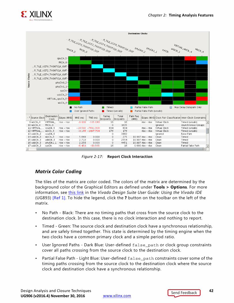
Details of the Clock Interaction ReportThe Clock Interaction report analyzes timing paths that cross from one clock domain (the source clock) into another clock domain (the destination clock). The Clock Interaction report helps to identify cases in which there may be data loss or metastability issues
After you run the Report Clock Interaction command, the results open in the Clock Interaction window. As shown in the following figure, the Clock Interaction Report displays as a matrix of clock domains with the source clocks in the vertical axis and the destination clocks in the horizontal axis.
Send FeedbackUG906 (v2016.4) November 30, 2016
Design Analysis and Closure Techniques 42UG906 (v2016.3) October 5, 2016 www.xilinx.com
Chapter 2: Timing Analysis Features
Matrix Color Coding
The tiles of the matrix are color coded. The colors of the matrix are determined by the background color of the Graphical Editors as defined under Tools > Options. For more information, see this link in the Vivado Design Suite User Guide: Using the Vivado IDE (UG893) [Ref 1]. To hide the legend, click the ? button on the toolbar on the left of the matrix.
• No Path - Black: There are no timing paths that cross from the source clock to the destination clock. In this case, there is no clock interaction and nothing to report.
• Timed - Green: The source clock and destination clock have a synchronous relationship, and are safely timed together. This state is determined by the timing engine when the two clocks have a common primary clock and a simple period ratio.
• User Ignored Paths - Dark Blue: User-defined false_path or clock group constraints cover all paths crossing from the source clock to the destination clock.
• Partial False Path - Light Blue: User-defined false_path constraints cover some of the timing paths crossing from the source clock to the destination clock where the source clock and destination clock have a synchronous relationship.
X-Ref Target - Figure 2-17
Figure 2-17: Report Clock Interaction
Send FeedbackUG906 (v2016.4) November 30, 2016

Design Analysis and Closure Techniques 43UG906 (v2016.3) October 5, 2016 www.xilinx.com
Chapter 2: Timing Analysis Features
• Timed (Unsafe) - Red: The source clock and destination clock have an asynchronous relationship. In this case, there is no common primary clock or no expandable period. For more information on asynchronous and unexpandable clocks, see this link in the Vivado Design Suite User Guide: Using Constraints (UG903) [Ref 6].
• Partial False Path (Unsafe) - Orange: This category is identical to Timed (Unsafe), except that at least one path from the source clock to the destination clock is ignored due to a false path exception.
• Max Delay Datapath Only - Gray: A set_max_delay -datapath_only constraint covers all paths crossing from the source clock to the destination clock.
IMPORTANT: The color of a cell in the matrix reflects the state of the constraints between clock domains, not the state of the timing paths worst slack between the domains. A green cell does not indicate that the timing is met, only that all timing paths that cross clock domains are properly timed, and that their clocks have a known phase relationship.
Clock Pair Classification
The Clock Pair Classification column provides information about the missing common primary clock, missing common node, and missing common period between two clocks, as well as the presence of a virtual clock.
The possible values, from the highest to the lowest priority, are listed below. As soon as a condition is detected, the report command does not perform the remaining checks.
• Ignored: When the clock pair is entirely covered by a Clock Group, a False Path, or a Max Delay Datapath Only, the analysis is ignored.
• Virtual Clock: At least one of the clocks is virtual, and common primary clock or common node checks do not apply.
• No Common Clock: The two clocks do not have a common primary clock.
• No Common Period: The periods of the two clocks are not expandable.
• Partial Common Node: The two clocks appear synchronous, but a subset of the crossing paths do not have a common node and cannot be safely timed.
• No Common Node: The two clocks appear synchronous, but the crossing paths do not have a common node.
• Clean: None of the above conditions applies.
Send FeedbackUG906 (v2016.4) November 30, 2016

Design Analysis and Closure Techniques 44UG906 (v2016.3) October 5, 2016 www.xilinx.com
Chapter 2: Timing Analysis Features
Filtering the Clocks
To filter the clocks displayed in the Clock Interaction report:
1. Select the Clock Interaction Options command in the toolbar.
2. Select the clocks to display.
The Clock Interaction Options command reduces the matrix complexity by limiting the number of clocks, but does not reduce the number of clock interactions reported in the table below the matrix. You can also show and hide the clocks that do not directly time a logical path in the design by clicking the Hide Unused Clocks button in the toolbar. Because these clocks do not contribute to WNS/TNS/WHS/THS computation, they are hidden by default.
Clock Pairs Slack Table
The table below the matrix provides a comprehensive overview of the timing slack for setup/recovery and/or for hold/removal for source/destination clock pair. It also shows useful information about path requirement of the worst paths, common primary clock and constraints status. See Figure 2-17. This provides details not displayed in the matrix above.
Sorting the Data
To sort the data in the table in increasing or decreasing values, single click multiple times on a column header.
X-Ref Target - Figure 2-18
Figure 2-18: Clock Interaction View Layers
Send FeedbackUG906 (v2016.4) November 30, 2016

Design Analysis and Closure Techniques 45UG906 (v2016.3) October 5, 2016 www.xilinx.com
Chapter 2: Timing Analysis Features
Selecting Cells and Rows
Selecting a cell in the matrix cross-selects a specific row of the table below.
Selecting a row from the table highlights a cell in the matrix above.
Table Columns
The table columns are:
• ID: A numeric ID for the source/destination clock pair being displayed.
• Source Clock: The clock domain from which the path originates.
• Destination Clock: The clock domain within which the path terminates.
• Edges (WNS): The clock edges used to calculate the worst negative slack for max delay analysis (setup/recovery).
• WNS (Worst Negative Slack): The worst slack calculated for various paths crossing the specified clock domains. A negative slack indicates a problem in which the path violates a required setup (or recovery) time.
• TNS (Total Negative Slack): The sum of the worst slack violation for all the endpoints that belong to paths crossing the specified clock domains.
• Failing Endpoints (TNS): The number of endpoints in the crossing paths that fail to meet timing. The sum of the violations corresponds to TNS.
• Total Endpoints (TNS): The total number of endpoints in the crossing paths.
• Path Req (WNS): The timing path requirement corresponding to the path reported in the WNS column. There can be several path requirements between any clock pairs if both rising and falling edges are active for at least one of the two clocks, or some timing exceptions have been applied on paths between the two clocks. The value reported in this column is not always the most challenging requirement.
For more information, see Path Requirement, page 156.
• Clock Pair Classification: Provide information about the common node and common period between the clock pair. From highest to lowest precedence: Ignored, Virtual Clock, No Common Clock, No Common Period, Partial Common Node, No Common Node, and Clean.
• Inter-Clock Constraints: Shows the constraints summary for all paths between the source clock and destination clock. The possible values are listed in the Matrix Color Coding, page 42. Following are example definitions of these constraints:
set_clock_groups -async -group wbClk -group usbClkset_false_path -from [get_clocks wbClk] -to [get_clocks cpuClk]
Send FeedbackUG906 (v2016.4) November 30, 2016

Design Analysis and Closure Techniques 46UG906 (v2016.3) October 5, 2016 www.xilinx.com
Chapter 2: Timing Analysis Features
When the min delay analysis is also selected (hold/removal), the following columns also appear in the table:
• Edges (WHS): The clock edges used to calculate the worst hold slack.
• WHS (Worst Hold Slack): The worst slack calculated for various paths crossing the specified clock domains. A negative slack indicates a problem in which the path violates a required hold (or removal) time.
• THS (Total negative Hold Slack): The sum of the worst slack violation for all the endpoints that belong to paths crossing the specified clock domains for min delay analysis (hold/removal).
• Failing Endpoints (THS): The number of endpoints in the crossing paths that fail to meet timing. The sum of the violations corresponds to THS.
• Total Endpoints (THS): The total number of endpoints in the crossing paths for min delay analysis (hold/removal).
• Path Req (WHS): The timing path requirement corresponding to the path reported in the WHS column. Like with WNS, there can be several possible path requirements for min delay analysis between two clocks, and the value reported in this column does not always correspond to the most challenging ones.
For more information, see Chapter 5, Performing Timing Analysis.
One or multiple clock pairs can be selected from the table. Report Timing between a selected source/destination clock pair can be run from the popup menu.
Exporting the Table
Run the Export to Spreadsheet command to export the table to an XLS file for use in a spreadsheet.
Send FeedbackUG906 (v2016.4) November 30, 2016
Design Analysis and Closure Techniques 47UG906 (v2016.3) October 5, 2016 www.xilinx.com
Chapter 2: Timing Analysis Features
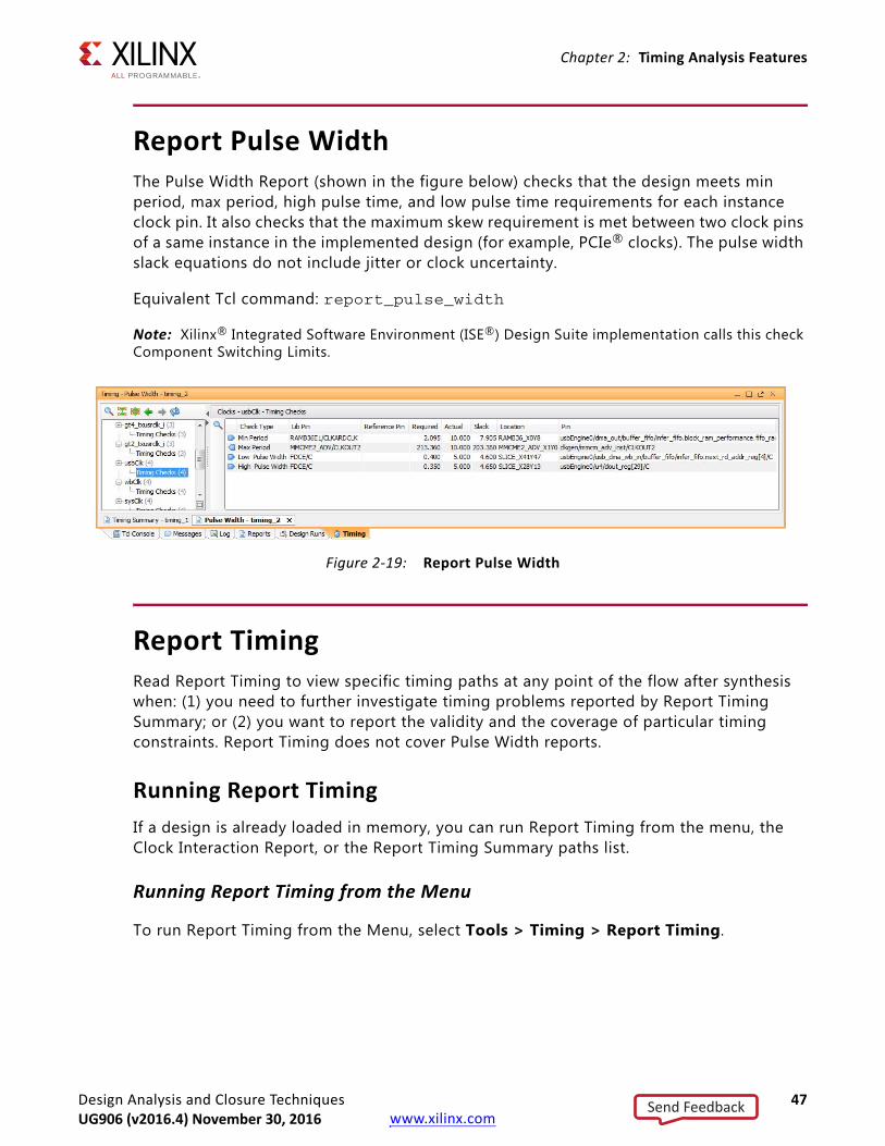
Report Pulse WidthThe Pulse Width Report (shown in the figure below) checks that the design meets min period, max period, high pulse time, and low pulse time requirements for each instance clock pin. It also checks that the maximum skew requirement is met between two clock pins of a same instance in the implemented design (for example, PCIe® clocks). The pulse width slack equations do not include jitter or clock uncertainty.
Equivalent Tcl command: report_pulse_width
Note: Xilinx® Integrated Software Environment (ISE®) Design Suite implementation calls this check Component Switching Limits.
Report TimingRead Report Timing to view specific timing paths at any point of the flow after synthesis when: (1) you need to further investigate timing problems reported by Report Timing Summary; or (2) you want to report the validity and the coverage of particular timing constraints. Report Timing does not cover Pulse Width reports.
Running Report TimingIf a design is already loaded in memory, you can run Report Timing from the menu, the Clock Interaction Report, or the Report Timing Summary paths list.
Running Report Timing from the Menu
To run Report Timing from the Menu, select Tools > Timing > Report Timing.
X-Ref Target - Figure 2-19
Figure 2-19: Report Pulse Width
Send FeedbackUG906 (v2016.4) November 30, 2016

Design Analysis and Closure Techniques 48UG906 (v2016.3) October 5, 2016 www.xilinx.com
Chapter 2: Timing Analysis Features
Running Report Timing from the Clock Interaction Report
To run Report Timing from the Clock Interaction Report:
1. Select a from/to clock pair.
2. Right-click and select Report Timing to run a report from or to the selected clocks.
Running Report Timing from a Paths List
To run Report Timing from a Paths List:
1. Select a path.
2. Right-click and select Report Timing to run a report between the selected path startpoint endpoint.
Equivalent Tcl command: report_timing
When setting specific Report Timing options, you can view the equivalent report_timing command syntax in:
• The Command field at the bottom of the dialog box, and
• The Tcl Console after execution
The report_timing options are listed along with the dialog box description in the following section.
Overall, the Report Timing options are identical to the Report Timing Summary options, plus a few additional filtering options.
Send FeedbackUG906 (v2016.4) November 30, 2016
Design Analysis and Closure Techniques 49UG906 (v2016.3) October 5, 2016 www.xilinx.com
Chapter 2: Timing Analysis Features
Report Timing Dialog Box
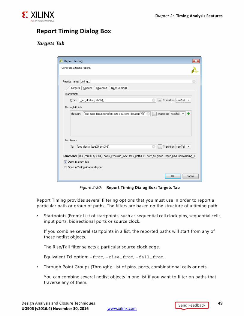
Targets Tab
Report Timing provides several filtering options that you must use in order to report a particular path or group of paths. The filters are based on the structure of a timing path.
• Startpoints (From): List of startpoints, such as sequential cell clock pins, sequential cells, input ports, bidirectional ports or source clock.
If you combine several startpoints in a list, the reported paths will start from any of these netlist objects.
The Rise/Fall filter selects a particular source clock edge.
Equivalent Tcl option: -from, -rise_from, -fall_from
• Through Point Groups (Through): List of pins, ports, combinational cells or nets.
You can combine several netlist objects in one list if you want to filter on paths that traverse any of them.
X-Ref Target - Figure 2-20
Figure 2-20: Report Timing Dialog Box: Targets Tab
Send FeedbackUG906 (v2016.4) November 30, 2016

Design Analysis and Closure Techniques 50UG906 (v2016.3) October 5, 2016 www.xilinx.com
Chapter 2: Timing Analysis Features
You can also specify several Through options to refine your filters and report paths that traverse all groups of through points in the same order as they are listed in the command options.
The Rise/Fall filter applies to the data edge.
RECOMMENDED: Use the default value (Rise/Fall).
Equivalent Tcl option: -through, -rise_through, -fall_through
• Endpoints (To): List of endpoints, such as input data pins of sequential cells, sequential cells, output ports, bidirectional ports or destination clock.
If you combine several endpoints in a list, the reported paths will end with any of these netlist objects.
In general, the Rise/Fall option selects a particular data edge. But if you specified a destination clock, it selects a particular clock edge.
Equivalent Tcl option: -to, -rise_to, -fall_to
The Targets tab in the Report Timing dialog box (Figure 2-20) defines the paths from the rising clock edge of usbClk, through any of the cpuEngine/or1200_cpu/sprs_dataout[*] nets, to either edge of cpuClk or sysClk.
Options Tab
The Options tab contains the following options:
• Reports
• Path Limits
• Path Display
Reports
• Path delay type: See Path delay type, page 22.
• Do not report unconstrained paths: By default, Report Timing reports paths that are not constrained if no path that matches the filters (from/through/to), is constrained. Check this box if you do not want to display unconstrained paths in your report.
Equivalent Tcl option: -no_report_unconstrained
Send FeedbackUG906 (v2016.4) November 30, 2016

Design Analysis and Closure Techniques 51UG906 (v2016.3) October 5, 2016 www.xilinx.com
Chapter 2: Timing Analysis Features
Path Limits
• Number of paths per group: See Report Timing Summary, page 20.
• Number of paths per endpoint: See Report Timing Summary, page 20.
• Limit paths to group: Filters on one or more timing path groups. Each clock is associated to a group. The Vivado IDE timing engine also creates default groups such as **async_default** which groups all the paths ending with a recovery or removal timing check.
Equivalent Tcl option: -group
Path Display
• Display paths with slack greater than: Displays the reported paths based on their slack value.
Equivalent Tcl option: -slack_greater_than
• Display paths with slack less than: See Report Timing Summary, page 20.
• Number of significant digits: See Report Timing Summary, page 20.
• Sort paths by: Displays the reported paths by group (default) or by slack. When sorted by group, the N worst paths for each group and for each type of analysis (-delay_type min/max/min_max) are reported.
The groups are sorted based on their individual worst path. The group with the worst violation appears at the top of the list. When sorted by slack, the N worst paths per type of analysis are reported (all groups combined) and are sorted by increasing slack.
Equivalent Tcl option: -sort_by
Advanced Tab
The Advanced tab has the same options as Report Timing Summary, page 20.
Timer Settings Tab
The Timer Settings tab has the same options as Report Timing Summary, page 20.
Send FeedbackUG906 (v2016.4) November 30, 2016

Design Analysis and Closure Techniques 52UG906 (v2016.3) October 5, 2016 www.xilinx.com
Chapter 2: Timing Analysis Features
Reviewing Timing Path DetailsAfter you click OK to run the report command, a new window opens. You can now review its content. You can view the N-worst paths reported for each type of selected analysis (min/max/min_max).
The following figure shows the Report Timing window in which both min and max analysis (SETUP and HOLD) were selected, and N=4.
Select any of these paths to view more details in the Path Properties window (Report tab).
X-Ref Target - Figure 2-21
Figure 2-21: Report Timing Paths List
X-Ref Target - Figure 2-22
Figure 2-22: Timing Path Properties Window
Send FeedbackUG906 (v2016.4) November 30, 2016

Design Analysis and Closure Techniques 53UG906 (v2016.3) October 5, 2016 www.xilinx.com
Chapter 2: Timing Analysis Features
To view the same details in a new window, double click the path.
For more information on timing path details, see Chapter 5, Performing Timing Analysis.
To access more analysis views for each path, right-click the path in the right pane and select one of the following actions:
• View the timing path Schematic.
• Rerun timing analysis on the same startpoint and endpoint of the selected path.
• Highlight the path in the Device and Schematic windows.
Filtering Paths with ViolationThe report displays the slack value of failing paths in red. To focus on these violations, click Show only failing checks mode.
Report DatasheetThe Report Datasheet command reports the operating parameters of the FPGA device for use in system-level integration.
Report Datasheet Dialog BoxIn the Vivado IDE, select Tools > Timing > Report Datasheet to open the Report Datasheet dialog box. See Figure 2-23.
Send FeedbackUG906 (v2016.4) November 30, 2016

Design Analysis and Closure Techniques 54UG906 (v2016.3) October 5, 2016 www.xilinx.com
Chapter 2: Timing Analysis Features
Report Datasheet Dialog Box: Options Tab
The Report Datasheet Dialog Box Options tab includes the following:
• Results name: Specifies the name for the returned results of the Report Datasheet command. The report opens in the Timing window of the Vivado IDE with the specified name.
Equivalent Tcl option: -name
• Sort by: Sorts the results by port name or by clock name.
Equivalent Tcl option: -sort_by
• Report all process corners separately: Reports the data for all defined process corners in the current design.
Equivalent Tcl option: -show_all_corners
X-Ref Target - Figure 2-23
Figure 2-23: Report Datasheet Dialog Box: Options Tab
Send FeedbackUG906 (v2016.4) November 30, 2016

Design Analysis and Closure Techniques 55UG906 (v2016.3) October 5, 2016 www.xilinx.com
Chapter 2: Timing Analysis Features
• Significant digits: Specifies the number of significant digits in the reported values. The default is three.
Equivalent Tcl option: -significant_digits
• Write results to file: Write the result to the specified file name. By default the report is written to the Timing window in the Vivado IDE.
Equivalent Tcl option: -file
• Overwrite / Append: When the report is written to a file, determines whether the specified file is overwritten, or new information is appended to an existing report.
Equivalent Tcl option: -append
• Ignore command errors: Executes the command quietly, ignoring any command line errors and returning no messages. Returns TCL_OK regardless of any errors encountered during execution.
Equivalent Tcl option: -quiet
• Suspend message limits: Temporarily overrides any message limits. Returns all messages from this command.
Equivalent Tcl option: -verbose
• Command: Displays the Tcl command line equivalent of the various options specified in the Report Datasheet dialog box.
• Open in a new tab: Opens the results in a new tab, or replaces the last tab opened by the Results window.
• Open in Timing Analysis layout: Resets the current view layout to the Timing Analysis view layout.
Send FeedbackUG906 (v2016.4) November 30, 2016

Design Analysis and Closure Techniques 56UG906 (v2016.3) October 5, 2016 www.xilinx.com
Chapter 2: Timing Analysis Features
Report Datasheet Dialog Box: Groups Tab
The Report Datasheet dialog box Groups tab allows you to define your own custom group of ports for analysis by specifying the reference port and additional ports to report. When Groups are not specified, the timer automatically finds the group of output ports based on the launching clock, and reports skew based on that clock.
The Report Datasheet dialog box Groups tab includes:
• Reference: Specifies the reference port for skew calculation. In most cases, this will be a clock port of a source synchronous output interface.
Equivalent Tcl option: -group
• Ports: Defines additional ports to report.
° Notice the +and - (plus and minus) buttons to the right of the Ports field.
- The + (plus) button specifies multiple groups, each with its own reference clock port allowing you to define a new group of ports, including a new reference port.
- The - (minus) button removes additional groups of ports as needed.
Report Datasheet Dialog Box: Timer Settings Tab
For details on this tab, see Timer Settings Tab, page 25.
X-Ref Target - Figure 2-24
Figure 2-24: Report Datasheet Dialog Box: Groups Tab
Send FeedbackUG906 (v2016.4) November 30, 2016

Design Analysis and Closure Techniques 57UG906 (v2016.3) October 5, 2016 www.xilinx.com
Chapter 2: Timing Analysis Features
Details of the Datasheet Report
General Information
This section provides details of the design and Xilinx® device, and the tool environment at the time of the report.
• Design Name: The name of the design
• Part: The target Xilinx part and speed file information.
• Version: The version of the Vivado tools used when the report was generated
• Date: The date and timestamp of the report
• Command: The command line used to generate the report
Input Ports Setup/Hold
The report displays worst-case setup and hold requirements for every input port with regard to the reference clock. The internal clock used to capture the input data is also reported.
Max/Min Delays for Output Ports
Shows worst-case maximum and minimum delays for every output port with regard to the reference clock. The internal clock used to launch the output data for is also reported.
Setup Between Clocks
For every clock pair, the worst-case setup requirements are reported for all clock edge combinations.
Setup/Hold for Input Buses
Input buses are automatically inferred and their worst-case setup and hold requirements are displayed. Worst case data window for the entire bus is the sum of the largest setup and hold values. If the input ports are constrained, the slack is also reported.
An optimal tap point is reported for input clocks with IDELAY defined. The optimal tap point can be used to configure IDELAY for balanced setup and hold slack.
The source offset is the delta between two windows. The first window is defined by the setup and hold time of the input port with regard to the clock. The second window is derived from the input delay and the clock period. If the input clock is offset with this value, then it will be in the center of the window.
Send FeedbackUG906 (v2016.4) November 30, 2016

Design Analysis and Closure Techniques 58UG906 (v2016.3) October 5, 2016 www.xilinx.com
Chapter 2: Timing Analysis Features
The following figure reports a design in which a DDR input bus, vsf_data[0:9], has a worst case data window of 1.663 ns. The ideal clock offset is 1.063 ns.
Note: The optimal tap point can be specified by using the Tcl command:
set_property IDELAY_VALUE 13 [get_cells idelay_clk]
Max/Min Delays for Output Buses
Output buses are automatically inferred and their worst case maximum and minimum delays are displayed. The bus skew is also reported. For bus skew calculation, one bit is considered as the reference and the offset of every other bit is calculated with respect to this reference bit. The worst offset is the skew for the entire bus.
Max/Min Delays for Groups
For Source Synchronous Output Interfaces, the output skew is desired with regard to the forwarded clock. A custom group report can be generated by specifying the reference port as the forwarded clock port. This table looks similar to “max/min delays for output buses” except the reference port is used as the reference bit for calculating source offset and bus skew.
Note: This section might be hidden if empty.
As an example, for a DDR output skew calculation, if multiple bits (for example, rldii_a[0-19], rldii_ba[0-3], rldii_ref_n, rldii_we_n) should be grouped together with regard to the forwarded clock port (rldii_ck_n[0]), the following command can be used:
X-Ref Target - Figure 2-25
Figure 2-25: Setup and Hold Delays for Input Buses
Send FeedbackUG906 (v2016.4) November 30, 2016

Design Analysis and Closure Techniques 59UG906 (v2016.3) October 5, 2016 www.xilinx.com
Chapter 2: Timing Analysis Features
report_datasheet -group [get_ports {rldii_ck_n[0] rldii_a[*] rldii_ba[*] rldii_ref_n rldii_we_n}] -name timing_1
The first port in the group list is considered the reference pin.
For all these sections, the worst case data is calculated from multi-corner analysis. If -show_all_corners is used, the worst case data is reported for each corner separately.
The following figure shows the report data sheet for this example.
X-Ref Target - Figure 2-26
Figure 2-26: Report Data Sheet Max/Min Delay Example
Send FeedbackUG906 (v2016.4) November 30, 2016

Design Analysis and Closure Techniques 60UG906 (v2016.3) October 5, 2016 www.xilinx.com
Chapter 2: Timing Analysis Features
Report ExceptionsYou can use the Report Exceptions command anywhere in the flow after the synthesis. The Report Exception command reports the following information:
• All the timing exceptions that have been set in the design and that are affecting timing analysis
• All the timing exceptions that have been set in the design but that are being ignored as they are overridden by other timing exception
The timing exceptions analyzed by the Report Exception command are (in the order of precedence):
• false paths
• max/min delays
• multicycle paths
The Report Exception is a powerful command to help debugging issues related to timing exceptions. Some designs have timing constraints with complex timing exceptions. Because the timing exceptions have different priorities, it can quickly become difficult to understand which timing exceptions might be partially or fully ignored by other exception(s). The Report Exception reports timing exceptions that are partially overridden, as well as those that are totally overridden. It also provides a hint to the overriding constraint(s).
Since Clock Groups constraints (set_clock_groups) are not exactly a timing exception, they are not covered in the summary table of all the timing exceptions affecting the design. However, when a timing exception is overridden by a clock group constraint, the clock group overriding the constraint is reported in the Status column of the table.
The Report Exception command is only available through the Tcl command line, using Tcl command report_exceptions.
For more information about the report_exceptions command line options, refer to this link in the Vivado Design Suite Tcl Command Reference Guide (UG835) [Ref 3]. For more information about the timing exception priority order, refer to this link in the Vivado Design Suite User Guide: Using Constraints (UG903) [Ref 6].
The report_exception command has three modes of operation:
• Reporting the timing exceptions affecting the timing analysis
• Reporting the timing exceptions being ignored
• Reporting the timing exceptions coverage
Send FeedbackUG906 (v2016.4) November 30, 2016

Design Analysis and Closure Techniques 61UG906 (v2016.3) October 5, 2016 www.xilinx.com
Chapter 2: Timing Analysis Features
Example: Reporting the Timing Exceptions Affecting the Timing AnalysisThis example describes how to take the design, shown in the following figure, through some timing exceptions. The design is fully constrained (clk and input/output delays defined relative to clk).
The first mode of operation of the Report Exception command is report_exception.
1. Select Window > Timing Constraints.
2. In the Timing Constraints window, add the following timing exceptions to the design:
set_multicycle_path 3 -from [get_cell int10_reg] -to [get_cell int20_reg]set_multicycle_path 4 -to [get_cell int20_reg]set_false_path -from [get_ports in6] -to [get_cell int20_reg]set_false_path -to [get_ports out5] set_false_path -to [get_cell int21_reg]set_false_path -from [get_ports in6] -to [get_ports out6]set_max_delay 5 -to [get_ports out6]set_min_delay 3 -from [get_cells int10_reg] -to [get_cell int20_reg]
The Timing Constraints window displays the timing constraints applied to the design, as shown in the following figure.
X-Ref Target - Figure 2-27
Figure 2-27: Fully Constrained Design for Timing Exception Example
Send FeedbackUG906 (v2016.4) November 30, 2016

Design Analysis and Closure Techniques 62UG906 (v2016.3) October 5, 2016 www.xilinx.com
Chapter 2: Timing Analysis Features
The actual Exception Report (report_exception) is shown in the following figure.
The Exceptions Report contains the following information:
• The Position column indicates the constraint position number. This is the same position number reported by the Timing Constraint Window, shown in Figure 2-28.
• The From/Through/To columns indicate the patterns or objects specified with -*from/-*through/-*to command line options (including all the rise/fall versions of those options). An asterisk is displayed when the associated option was not specified.
• The Setup/Hold columns indicate whether the constraint applies to setup check, hold check, or both. The naming conventions for the Setup/Hold columns are shown in the following table:
X-Ref Target - Figure 2-28
Figure 2-28: Constraints Window Displaying Timing Constraint Changes
X-Ref Target - Figure 2-29
Figure 2-29: Report Exception
Table 2-1: Setup/Hold Column Naming Conventions
Short Name Timing Exception
cycles= set_multicycle_path
false set_false_path
max= set_max_delay
max_dpo= set_max_delay -datapath_only
min= set_min_delay
Send FeedbackUG906 (v2016.4) November 30, 2016

Design Analysis and Closure Techniques 63UG906 (v2016.3) October 5, 2016 www.xilinx.com
Chapter 2: Timing Analysis Features
• The Status column reports a message when a constraint is partially overridden by another timing exception. The naming conventions for the Status column are shown in the following table:
Note: The clock group is only reported in the Status column of the report_timing -ignored command when a clock group constraint overrides another timing exception.
In this example, there are two messages regarding partially overridden constraints:
• The timing constraint position 5 (set_multicycle_path 4 -to [get_cell int20_reg] based on the Timing Constraints Window) is partially overridden by the multicycle constraint position 4 (set_multicycle_path 3 -from [get_cell int10_reg] -to [get_cell int20_reg]) and by the false path constraint position 6 (set_false_path -from [get_ports in6] -to [get_cell int20_reg]).
• The timing constraint position 10 (set_max_delay 5 -to [get_ports out6]) is partially overridden by the false path position 9 (set_false_path -from [get_ports in6] -to [get_ports out6]).
Reporting the Timing Exceptions Being IgnoredThe second mode of operation of the Report Exception command is report_exception -ignored.
To illustrate, add the following timing exceptions on the top of the previous ones:
set_max_delay 5 -to [get_ports out5]set_multicycle_path 1 -hold -to [get_cell int21_reg]set_multicycle_path 2 -setup -to [get_ports out6]set_false_path -from [get_cell int11_reg] -to [get_cell int20_reg]
All those exceptions are either already covered by a timing exception from the previous section (reporting the timing exceptions affecting the timing analysis) or target a non-existing path (there is no physical connection between the registers int11_reg and int20_reg).
After adding these four constraints, the Timing Constraints Window looks like Figure 2-30.
Table 2-2: Status Column Naming Conventions
Short Timing Exception
MCP multicycle path
FP false path
MXD max delay
MND min delay
CG clock group
Send FeedbackUG906 (v2016.4) November 30, 2016

Design Analysis and Closure Techniques 64UG906 (v2016.3) October 5, 2016 www.xilinx.com
Chapter 2: Timing Analysis Features
The Exceptions Report (report_exception -ignored) is as shown in the following figure:
Note: The Status column provides some explanations why the timing exceptions are being ignored.
Reporting the Timing Exceptions CoverageThe Vivado tools can generate a detailed coverage of each valid timing exception applied to the design. All the timing exceptions are reported, including those that are fully overridden or that do not have path between startpoints and endpoints. The coverage report can be large, depending on the number of timing exceptions and complexity of the design.
The coverage report is generated using the -coverage command line option: report_exceptions -coverage.
The report includes, for each valid timing exception, the following information:
• Constraint position number
• Number of objects selected by the -from/-through/-to command line options
• All the clock domains involved in the timing exception, as well as the number of endpoints for each endpoint clock domain
• A summary list of cells involved in the startpoints and endpoints
X-Ref Target - Figure 2-30
Figure 2-30: Timing Constraints Window
X-Ref Target - Figure 2-31
Figure 2-31: Exceptions Report
Send FeedbackUG906 (v2016.4) November 30, 2016

Design Analysis and Closure Techniques 65UG906 (v2016.3) October 5, 2016 www.xilinx.com
Chapter 2: Timing Analysis Features
Below is an abstract from a coverage report from a different design:
Exception: set_false_path -from [get_pins {SW_FPGA_CORE/U_RST/st_asrst[0]/C}]+ Position: 74+ Objects: -from: 1 pins+ Clock Domains Details: +Domain : CLK_OUT2_PLL3 -> CLK_OUT1_PLL3 -Source Clock: CLK_OUT2_PLL3 -Destination Clock: CLK_OUT1_PLL3 -Endpoints: 154277 +Domain : CLK_OUT2_PLL3 -> CLK_OUT2_PLL3 -Source Clock: CLK_OUT2_PLL3 -Destination Clock: CLK_OUT2_PLL3 -Endpoints: 9933 +Domain : CLK_OUT2_PLL3 -> CLK_OUT4_PLL3 -Source Clock: CLK_OUT2_PLL3 -Destination Clock: CLK_OUT4_PLL3 -Endpoints: 434 +Domain : CLK_OUT2_PLL3 -> clk_pll_i -Source Clock: CLK_OUT2_PLL3 -Destination Clock: clk_pll_i -Endpoints: 7193+ Startpoint Details: FDPE/C=1 + Endpoint Details: FDCE/CLR=169792 FDCE/D=7 FDPE/PRE=2038
When a timing exception does not have any path between the startpoints and endpoints, the coverage report has empty fields. For example:
Exception: set_false_path -from [get_cells int11_reg] -to [get_cells int20_reg]+ Position: 15+ Objects: -from: 1 cells -to: 1 cells+ Clock Domains Details:+ Startpoint Details: + Endpoint Details:
The coverage reports can be used to improve the effectiveness of how the timing exceptions are written.
Below is another example of coverage report for a set_multicycle_path constraint:
Exception: set_multicycle_path -start -from [get_pins {sr_b*_rd_dat[*]/C}] -to [get_pins {ar_b*_rd_dat[*]/D}] 4+ Position: 75+ Objects: -from: 486 pins -to: 486 pins+ Clock Domains Details: +Domain : CLK_OUT1_PLL3 -> CLK_OUT2_PLL3 -Source Clock: CLK_OUT1_PLL3 -Destination Clock: CLK_OUT2_PLL3 -Endpoints: 24+ Startpoint Details: FDCE/C=4 + Endpoint Details: FDCE/D=24
Send FeedbackUG906 (v2016.4) November 30, 2016

Design Analysis and Closure Techniques 66UG906 (v2016.3) October 5, 2016 www.xilinx.com
Chapter 2: Timing Analysis Features
In the above example, the get_pins commands used to build the -from/-to command line options return each 486 pins. However, paths between 4 startpoints and 24 endpoints are covered. This means that other combinations of startpoints and endpoints do not have physical paths.
Report Clock Domain CrossingsThe Clock Domain Crossings (CDC) report performs a structural analysis of the clock domain crossings in your design. You can use this information to identify potentially unsafe CDCs, which will lead to metastability or data coherency issues. While the CDC report is similar to the Clock Interaction Report, the CDC report focuses on structures and their timing constraints, but does not provide information related to timing slack.
OverviewBefore generating the CDC report, you must ensure that the design has been properly constrained and there are no missing clock definitions. Report CDC only analyzes and reports paths where both source and destination clocks have been defined. Report CDC performs structural analysis:
• On all paths between asynchronous clocks.
• Only on paths between synchronous clocks that have the following timing exceptions:
° Clock groups
° False Path
° Max Delay Datapath Only
Synchronous clock paths with no such timing exception are assumed to be safely timed and are not analyzed by the CDC engine. The Report CDC operates without taking into consideration any net or cell delays.
TerminologyThe terminology for safe, unsafe, and endpoints is different in the context of Cross Domain Crossing (CDC) and inter-clock timing analysis.
In the context of CDC, an asynchronous crossing is safe when proper synchronization circuitry is used to prevent metastability. For example, a safe single-bit CDC can be implemented by a synchronizer, which is a chain of registers with same clock and control signals. A safe multi-bit CDC can be implemented with a MUX Hold circuitry or a Clock Enabled Controlled circuitry.
Send FeedbackUG906 (v2016.4) November 30, 2016

Design Analysis and Closure Techniques 67UG906 (v2016.3) October 5, 2016 www.xilinx.com
Chapter 2: Timing Analysis Features
Conversely, an unsafe CDC is when the CDC analysis engine does not recognize a known safe synchronization circuit on an asynchronous CDC path.
The number of endpoints reported for CDC between two clock domains can be different than the number of endpoints reported by the timing analysis commands. For example, an asynchronous reset synchronizer involves multiple timing path endpoints. However, the synchronization circuitry is reported as a single element and therefore as a single CDC endpoint. Similarly, a multi-bit CDC contains multiple single bit crossings but is reported as a single CDC endpoint. However, the same bus is reported as multiple timing endpoints by other timing reports.
IMPORTANT: Because report_clock_interaction and report_cdc have different purposes, do not compare the number of endpoints reported by each command. In the context of report_clock_interaction, safe/unsafe refers to the ability for the timing analysis engine to provide a slack that matches the worst situation in hardware. For report_cdc, safe/unsafe refers to the type of CDC circuitry implemented in the design.
Running Report Clock Domain CrossingsWhen you run Report CDC from the Vivado IDE, it provides all the details for the CDC paths between the specified clocks by default. When you run Report CDC from the Tcl Console, however, it only prints the Summary by Clock Pairs table. You must specify the -details option in order to report all the details as in the GUI mode. Reporting the details can create very long files or log files.
To run the Report Clock Domain Crossings in the Vivado IDE, select Tools > Timing > Report CDC.
Equivalent Tcl command: report_cdc -name cdc_1
In the Vivado IDE, the Report CDC dialog box includes the following fields, as shown in Figure 2-32:
• Results Name Field
• Clocks Field (From/To)
• File Output Field
• Options Field
Send FeedbackUG906 (v2016.4) November 30, 2016
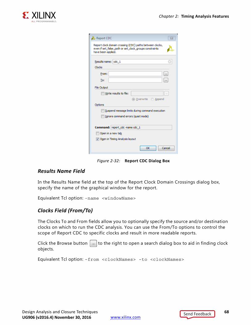
Design Analysis and Closure Techniques 68UG906 (v2016.3) October 5, 2016 www.xilinx.com
Chapter 2: Timing Analysis Features
Results Name Field
In the Results Name field at the top of the Report Clock Domain Crossings dialog box, specify the name of the graphical window for the report.
Equivalent Tcl option: -name <windowName>
Clocks Field (From/To)
The Clocks To and From fields allow you to optionally specify the source and/or destination clocks on which to run the CDC analysis. You can use the From/To options to control the scope of Report CDC to specific clocks and result in more readable reports.
Click the Browse button to the right to open a search dialog box to aid in finding clock objects.
Equivalent Tcl option: -from <clockNames> -to <clockNames>
X-Ref Target - Figure 2-32
Figure 2-32: Report CDC Dialog Box
Send FeedbackUG906 (v2016.4) November 30, 2016

Design Analysis and Closure Techniques 69UG906 (v2016.3) October 5, 2016 www.xilinx.com
Chapter 2: Timing Analysis Features
File Output Field
The File Output field allows you to optionally specify a file into which to write the results. You can overwrite the file or append to it.
Equivalent Tcl option: -file <fileName> -append
Options Field
The Options field allows you to:
• Suspend message limits
Equivalent Tcl option: -verbose
• Ignore command errors
Equivalent Tcl option: -quiet
Understanding the Clock Domain Crossings Report RulesReport CDC tries to match each CDC path to a known CDC topology. Each CDC topology is associated with one or several CDC rules, as presented in Table 2-3. Note that you cannot modify the severity of the rules as with DRCs and Messages. Simplified schematics and descriptions of the CDC Topologies being detected are included in Simplified Schematics of the CDC Topologies, page 76.
Table 2-3: CDC Rules and Description
CDC Topology CDC Rule Severity Description
Single-bit CDC CDCH-1 Critical A single-bit CDC path is not synchronized or has unknown CDC circuitry.
CDCH-2 Warning A single-bit CDC path is synchronized with a 2+ stage synchronizer but the ASYNC_REG property is missing on all or some of the synchronizer flip-flops.
CDCH-3 Info A single-bit CDC path is synchronized with a 2+ stage synchronizer and the ASYNC_REG property is present.
Multi-bit CDC CDCH-4 Critical A multi-bit bus CDC path is not synchronized or has unknown CDC circuitry.
CDCH-5 Warning A multi-bit bus CDC path is synchronized with a 2+ stage synchronizer but the ASYNC_REG property is missing on all or some of the synchronizer flip-flops.
CDCH-6 Warning A multi-bit bus CDC path is synchronized with a 2+ stage synchronizer and the ASYNC_REG property is present.
Send FeedbackUG906 (v2016.4) November 30, 2016

Design Analysis and Closure Techniques 70UG906 (v2016.3) October 5, 2016 www.xilinx.com
Chapter 2: Timing Analysis Features
Reviewing the Clock Domain Crossings Report SectionsIn the GUI mode, three sections are generated by default:
• Summary by Clock Pair
• Summary by Type
• Detailed Report
The summary sections provide a convenient overview of the issues that need review and possibly a change in the design. These sections can be used to navigate to the violations of highest Severity where additional information is contained within the Detailed Report section.
Note: By default, only the Summary by clock pair section is generated when running the report in text mode.
Asynchronous Reset CDCH-7 Critical An asynchronous signal (clear or preset) is not synchronized or has unknown CDC circuitry.
CDCH-8 Warning An asynchronous signal (clear or preset) is synchronized but the ASYNC_REG property is missing on all or some of the synchronizer flip-flops.
CDCH-9 Info An asynchronous reset is synchronized and the ASYNC_REG property is present.
Combinatorial Logic CDCH-10 Critical Combinatorial logic has been detected in the fanin of a synchronization circuit.
Fanout CDCH-11 Critical A fanout has been detected before a synchronization circuit.
Multi-Clock Fanin CDCH-12 Critical Data from multiple clocks are found in the fanin of a synchronization circuit.
non-FD primitive CDCH-13 Critical CDC detected on a non-FD primitive.
CE-controlled CDC CDCM-1 Warning Clock Enable controlled CDC.
Mux-controlled CDC CDCM-2 Warning Multiplexer controlled CDC.
Mux Data Hold CDC CDCM-3 Warning Multiplexer data holding CDC.
HARD_SYNC primitive CDCH-18 Info A signal is synchronized with a HARD_SYNC primitive.
Table 2-3: CDC Rules and Description (Cont’d)
CDC Topology CDC Rule Severity Description
Send FeedbackUG906 (v2016.4) November 30, 2016

Design Analysis and Closure Techniques 71UG906 (v2016.3) October 5, 2016 www.xilinx.com
Chapter 2: Timing Analysis Features
Summary by Clock Pair
In the Summary (by clock pair) section, useful information about the number of CDC paths between two clocks are presented, along with the severity of the most critical issue found among these paths. The table includes the following columns:
• Severity: Reports the worst severity of all CDC paths from/to the listed clocks. Values are Info, Warning, or Critical.
• Source Clock: Shows the name of the CDC Source Clock.
• Destination Clock: Shows the name of the CDC Destination Clock.
• CDC Type: Reflects the relationship between two clocks and their dominant timing exception, if any. Possible types are:
° Safely Timed: All CDC paths are safely timed because the clocks are synchronous and accurate timing is not prevented by a timing exception.
° User Ignored: All CDC paths are covered by set_false_path or set_clock_groups.
° No Common Primary Clock: The CDC clocks are asynchronous and at least 1 CDC path is normally timed between two clocks that do not have a common primary clock.
° No Common Period: The CDC clocks are asynchronous and at least 1 CDC path is normally timed between two clocks that do not have a common period. For the definition of clocks with no common period, refer to Understanding the Basics of Timing Analysis, page 152.
• Exceptions: The timing exceptions applied to the CDC (if any) are:
° None: No timing exceptions exist on the CDC paths.
° Asynch Clock Groups: The set_clock_groups -asynchronous exception was applied to the CDC clocks.
° Exclusive Clock Groups: The set_clock_groups -exclusive exception was applied to the CDC clocks.
° False Path: The set_false_path exception was applied to from/to the CDC clocks or to all CDC paths.
° Max Delay Datapath Only: The set_max_delay -datapath_only exception was applied to all CDC paths. Note that “Max Delay Datapath Only” is reported when at least one CDC path is only covered by set_max_delay -datapath_only, while all other CDC paths are ignored due to set_false_path constraints.
° Partial Exceptions: A mix of set_false_path and set_max_delay -datapath_only constraints are applied to some of the CDC paths, and at least one CDC path is normally timed.
Send FeedbackUG906 (v2016.4) November 30, 2016

Design Analysis and Closure Techniques 72UG906 (v2016.3) October 5, 2016 www.xilinx.com
Chapter 2: Timing Analysis Features
• Endpoints: The total number of CDC path endpoints. This is the sum of Safe, Unsafe, and Unknown endpoints. In this context, an endpoint is a sequential cell input data pin. An FD cell can be counted several times depending on the D, CE, and SET/RESET/CLEAR/PRESET connectivity. For some CDC topologies, only one endpoint is counted while there are effectively several paths crossing the clock domain boundary to reach the CDC structure. For example, in an asynchronous reset synchronizer, several CLEAR pins are connected to the crossing net, but only the first pin of the synchronizer chain is counted.
• Safe: The number of safe CDC path endpoints. Safe endpoints are endpoints on CDC paths identified as:
° Asynchronous Clocks with known Safe CDC structures
° Synchronous Clocks with exceptions and known Safe CDC structures
° Synchronous Clocks without exceptions that are safely timed regardless of the CDC structure
° CDC synchronized with HARD_SYNC macro
• Unsafe: The number of CDC path endpoints that are recognized as having an unsafe structure. The unsafe endpoints are CDCH-10, CDCH-11, CDCH-12 and CDCH-13.
° Combinatorial Logic Topology
° Fanout Topology
° Multi-Clock Fan-in Topology
° non-FD primitive Topology
• Unknown: The number of unknown CDC path endpoints. No CDC structure can be matched on these endpoints or an unknown CDC circuitry has been detected (CDCH1, CDCH4 and CDCH-7).
• No ASYNC_REG: The number of identified synchronizers that are missing the ASYNC_REG property on at least one of the two first FD cells of the chain.
The following figure shows an example of a Summary by clock pair section.
Send FeedbackUG906 (v2016.4) November 30, 2016

Design Analysis and Closure Techniques 73UG906 (v2016.3) October 5, 2016 www.xilinx.com
Chapter 2: Timing Analysis Features
Summary by Type
The Summary by Type table is convenient for quickly reviewing the nature of CDC structures found in the current report. An example is shown in Figure 2-34.
X-Ref Target - Figure 2-33
Figure 2-33: Summary by Clock Pair Section
X-Ref Target - Figure 2-34
Figure 2-34: Summary by Type Table
Send FeedbackUG906 (v2016.4) November 30, 2016

Design Analysis and Closure Techniques 74UG906 (v2016.3) October 5, 2016 www.xilinx.com
Chapter 2: Timing Analysis Features
The Summary by Type table includes the following columns:
• Severity: Reports the severity of the CDC Rule as Info, Warning, or Critical.
• ID: Unique identification number of the CDC Rule, as listed in Table 2-3.
• Count: Number of occurrences of the CDC Rule in the entire report.
• Description: Short description of the CDC Rule.
When analyzing the summary tables, it is important to start with the highest severity. Severity levels are:
• Critical: This severity is for CDC paths with unknown or unsafe CDC Structures. You must review each individual path to either fix the structure by modifying the RTL, or waive the issue. The path details are generated by default when using the Vivado IDE, and only when -details is used with report_cdc on the command line.
° There is some combinatorial logic on the crossing net or several source clocks are found in the fanin of the crossing net. This can degrade the Mean Time Between Failures (MTBF) characteristics.
° There is a fanout on the crossing net to the same destination clock domain. This can lead to data coherency problems.
• Warning: This severity is for CDC paths with known CDC Structures that are safe but non-ideal due to one of the following reasons:
° At least one of the two first synchronizer flip-flops does not have the ASYNC_REG property set to 1 (or true)
° The CDC structure identified requires functional correctness that the CDC engine cannot verify. These structures are Clock Enable Controlled, MUX Controlled, and MUX Data-Hold controlled CDC topologies.
• Info: This severity indicates that CDC structures are all safe and properly constrained.
Detailed Report
The Report CDC details can be viewed by looking at the CDC Details section in the report. You can use the detailed report to view the schematic of the selected path (by pressing the F4 key), view the timing report, or generate a new timing report by right-clicking on the individual entry.
You can use the timing reports and schematics to review unexpected CDC paths in the design, to identify incorrect or missing timing exceptions, and to find missing ASYNC_REG properties. An example of the CDC Detailed Report is shown in the following figure.
Send FeedbackUG906 (v2016.4) November 30, 2016

Design Analysis and Closure Techniques 75UG906 (v2016.3) October 5, 2016 www.xilinx.com
Chapter 2: Timing Analysis Features
The CDC Detailed Report table includes the following columns:
• Severity: Reports the severity of the CDC Rule as Info, Warning, or Critical.
• ID: The unique identification number of the CDC Rule, as listed in Table 2-3, page 69.
• Description: A short description of the CDC Rule.
• Depth: The number of synchronizer stages found (only applies to synchronizer topologies).
• Exception: The timing exception applied to the CDC path.
• Source (From): The CDC timing path startpoint.
• Destination (To): The CDC timing path endpoint.
• Category: Displays Safe, Unsafe, Unknown, etc.
• Source Clock (From): The name of the source clock.
Note: This column displays only when you click CDC Details (left column of Timing-Report CDC window)
• Destination Clock (To): The name of the destination clock.
Note: This column displays only when you click CDC Details (left column of Timing-Report CDC window)
IMPORTANT: The CDC report can flag issues in some of the Xilinx IPs because the CDC engine does not recognize all possible CDC topologies and does not provide a built-in waiver mechanism. More information can be found in each Xilinx IP Product Guide.
X-Ref Target - Figure 2-35
Figure 2-35: CDC Detailed Report
Send FeedbackUG906 (v2016.4) November 30, 2016

Design Analysis and Closure Techniques 76UG906 (v2016.3) October 5, 2016 www.xilinx.com
Chapter 2: Timing Analysis Features
Simplified Schematics of the CDC TopologiesSimplified schematics of the CDC Topologies along with brief descriptions are shown in the following sections. In all schematics, the Source Clock net (typically clk_a) is highlighted in blue and the Destination Clock net (typically clk_b) is highlighted in orange.
Single-Bit Synchronizer
The simplified topology of a Single-bit synchronizer is shown in Figure 2-36. The ASYNC_REG property must be set on at least the first two flip flops of the synchronization chain. The synchronizer depth is defined by the number of chained flip-flops that share the same control signals.
If the CLEAR or PRESET pins of the flip-flops are also connected to an asynchronous source, the synchronizer is only reported as a single-bit synchronizer and not as an asynchronous reset synchronizer.
X-Ref Target - Figure 2-36
Figure 2-36: Simplified Topology of a Single-Bit Synchronizer
Send FeedbackUG906 (v2016.4) November 30, 2016

Design Analysis and Closure Techniques 77UG906 (v2016.3) October 5, 2016 www.xilinx.com
Chapter 2: Timing Analysis Features
Multi-Bit Synchronizer
The multi-bit synchronizer topology that is detected is equivalent to multiple single-bit synchronizers grouped together based on the startpoint-endpoint names and matching CDC rules. In this context, a bus is defined by the startpoint and endpoint cell names and not by the net names. The expected bus name format is baseName[index]. Also the startpoint and endpoint indexes must match. The following figure shows an example of a multi-bit synchronizer that is 2 bits wide.
If all bits of a CDC bus do not match the same CDC rule, the bus is reported as single bits or bus segments with continuous indexes that match a same CDC rule.
It is essential to understand that having a register-based synchronizer on a bus does not make the domain crossing safe for the bus. This is the reason the CDC rule CDC-6 is a Warning, as the tool cannot decide whether or not the topology is adequate for the design. It is up to the designer to confirm the safety of the CDC.
If the bus is Gray coded, it is safe to use a register-based synchronizer on all the bits of the bus as long as the adequate timing constraints have been set on the bus to make sure that no more than one data at a time can be captured by the receiving domain.
If the bus is not Gray coded, other synchronizer topologies should be used instead, such as CE Controlled CDC or MUX Controlled CDC.
X-Ref Target - Figure 2-37
Figure 2-37: Multi-Bit Synchronizer with 2-Bit Width
Send FeedbackUG906 (v2016.4) November 30, 2016

Design Analysis and Closure Techniques 78UG906 (v2016.3) October 5, 2016 www.xilinx.com
Chapter 2: Timing Analysis Features
Asynchronous Reset Synchronizer
The synchronization of an asynchronous reset is shown in the following figure for CLEAR-based synchronization, and in Figure 2-39 for PRESET-based synchronization. The FF1 cell is respectively connected to the synchronized clear or preset signals and their deassertion can safely be timed against clk_a. Note that flip-flops with CLEAR and PRESET cannot be mixed within an asynchronous reset synchronizer.
X-Ref Target - Figure 2-38
Figure 2-38: CLEAR-Based Asynchronous Reset Synchronizer
X-Ref Target - Figure 2-39
Figure 2-39: PRESET-Based Asynchronous Reset Synchronizer
Send FeedbackUG906 (v2016.4) November 30, 2016

Design Analysis and Closure Techniques 79UG906 (v2016.3) October 5, 2016 www.xilinx.com
Chapter 2: Timing Analysis Features
Combinatorial Logic
In the combinatorial logic simplified example presented in the following figure, a logic function represented by the LUT3 is placed between the CDC from clk_a to clk_b synchronizers.
This structure is traditionally not recommended due the potential occurrence of glitches on the output of the combinatorial logic, which is captured by the synchronizer and propagated downward to the rest of the design.
X-Ref Target - Figure 2-40
Figure 2-40: Combinatorial Logic Simplified Example
Send FeedbackUG906 (v2016.4) November 30, 2016

Design Analysis and Closure Techniques 80UG906 (v2016.3) October 5, 2016 www.xilinx.com
Chapter 2: Timing Analysis Features
Fanout
In the simplified Fanout example shown in the following figure, the source flip-flop drives a net that is synchronized three times in the clk_b domain highlighted in red. This structure is not recommended as it can lead to data coherency issues in the destination clock domain because the latency through the synchronizers is bounded but not cycle-accurate.
Note: A fanout of N to N different clock domains is not a CDC problem and does not trigger a CDCH-11 violation.
X-Ref Target - Figure 2-41
Figure 2-41: Simplified Fanout Example
Send FeedbackUG906 (v2016.4) November 30, 2016

Design Analysis and Closure Techniques 81UG906 (v2016.3) October 5, 2016 www.xilinx.com
Chapter 2: Timing Analysis Features
Multi-Clock Fanin
In the Multi-Clock Fanin example shown in the following figure, both clk_a and clk_x are transferring data through combinatorial logic (LUT2) to the synchronizer circuit in the clk_b domain. It is recommended to first synchronize the source data from clk_a and clk_x individually before combining them via some glue logic. This improves the MTBF characteristics of the overall CDC structure, and it prevents glitches to propagate to the destination clock domain.
X-Ref Target - Figure 2-42
Figure 2-42: Multi-Clock Fanin Example
Send FeedbackUG906 (v2016.4) November 30, 2016

Design Analysis and Closure Techniques 82UG906 (v2016.3) October 5, 2016 www.xilinx.com
Chapter 2: Timing Analysis Features
Non-FD Primitive
In the Non-FD Primitive example presented in the following figure, a CDC is occurring between a FDRE and a RAMB while no synchronization logic exists inside the RAMB primitive. Even if a single stage flip-flop connected to clk_b is inserted in front of the RAMB, it is still considered an inadequate synchronizer due to the routing distance between the FDRE and RAMB cells.
Note: This rule does not include the HARD_SYNC macro, which is detected and covered by CDCH-18.
X-Ref Target - Figure 2-43
Figure 2-43: Non-FD Primitive Example
Send FeedbackUG906 (v2016.4) November 30, 2016

Design Analysis and Closure Techniques 83UG906 (v2016.3) October 5, 2016 www.xilinx.com
Chapter 2: Timing Analysis Features
CE-controlled CDC
In the CE-controlled CDC example shown in the following figure, the clock enable signal is synchronized in the destination clk_b domain before being used to control the crossing flip-flops.
The CDC engine only checks that the signal connected to FF3/CE is also launched by clk_b. There is no restriction on how the clock enable signal is synchronized, as long as it is separately reported as a safe CDC path. Also, you are responsible for constraining the latency from the clk_a domain to FF3, which is usually done by a set_max_delay -datapath_only constraint.
X-Ref Target - Figure 2-44
Figure 2-44: CE-Controlled CDC Example
Send FeedbackUG906 (v2016.4) November 30, 2016

Design Analysis and Closure Techniques 84UG906 (v2016.3) October 5, 2016 www.xilinx.com
Chapter 2: Timing Analysis Features
Mux-Controlled CDC
In the Mux-controlled CDC example, shown in the following figure, the multiplexer select signal is synchronized to the destination clock domain, clk_b.
Similar to CE-controlled CDC, there is no restriction on how the select signal is synchronized as long as it is reported as safe individually and the user is responsible for constraining the crossing delay on FF2_c.
X-Ref Target - Figure 2-45
Figure 2-45: Mux-Controlled CDC Example
Send FeedbackUG906 (v2016.4) November 30, 2016
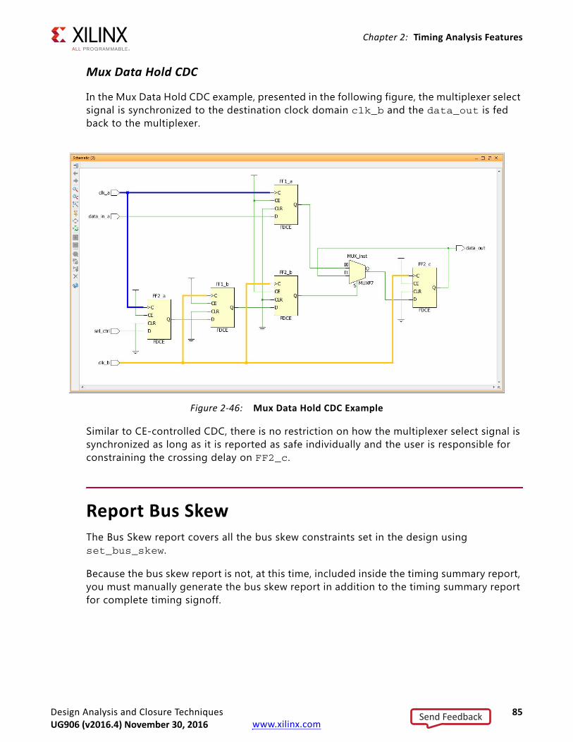
Design Analysis and Closure Techniques 85UG906 (v2016.3) October 5, 2016 www.xilinx.com
Chapter 2: Timing Analysis Features
Mux Data Hold CDC
In the Mux Data Hold CDC example, presented in the following figure, the multiplexer select signal is synchronized to the destination clock domain clk_b and the data_out is fed back to the multiplexer.
Similar to CE-controlled CDC, there is no restriction on how the multiplexer select signal is synchronized as long as it is reported as safe individually and the user is responsible for constraining the crossing delay on FF2_c.
Report Bus SkewThe Bus Skew report covers all the bus skew constraints set in the design using set_bus_skew.
Because the bus skew report is not, at this time, included inside the timing summary report, you must manually generate the bus skew report in addition to the timing summary report for complete timing signoff.
X-Ref Target - Figure 2-46
Figure 2-46: Mux Data Hold CDC Example
Send FeedbackUG906 (v2016.4) November 30, 2016

Design Analysis and Closure Techniques 86UG906 (v2016.3) October 5, 2016 www.xilinx.com
Chapter 2: Timing Analysis Features
Running Report Bus SkewThe bus skew report is only available from the command line with the report_bus_skew Tcl command. The command shares many options with the report_timing command to filter and format the output report.
Reviewing Bus Skew Path DetailsThe bus skew report includes two sections:
1. A bus skew report summary
2. A bus skew report by constraint
Report Summary Section
The Report Summary section reports all the set_bus_skew constraints defined in the design. The following information is reported for each constraint:
• Id: constraint Id referred later in the report (makes it easier to search for that constraint inside the report)
• From: pattern provided for the set_bus_skew -from option
• To: pattern provided for the set_bus_skew -to option
• Corner: corner (Slow or Fast) in which the worst bus skew was computed
• Requirement: bus skew target value
• Actual: worst bus skew computed across all the paths covered by the constraint
• Slack: difference between the worst bus skew and the constraint requirement
In the following example, the design has only one bus skew constraint with a 1 ns requirement. The worst skew among all the paths covered by the constraint is 1.107 ns.
Report Per Constraint Section
The Report Per Constraint section provides more details for each of the set_bus_skew constraints. Each reported constraint includes two parts:
1. Detailed summary of the paths covered by the constraint
2. Detailed timing paths for the paths reported in the Per Constraint summary
X-Ref Target - Figure 2-47
Send FeedbackUG906 (v2016.4) November 30, 2016

Design Analysis and Closure Techniques 87UG906 (v2016.3) October 5, 2016 www.xilinx.com
Chapter 2: Timing Analysis Features
The detailed summary table provides the following information:
• From Clock: startpoints clock domain
• To Clock: endpoints clock domain
• Endpoint Pin: endpoint pin involved in the reported path
• Reference Pin: reference pin used to compute the skew. Each row of this table can refer to a different reference pin.
• Corner: Fast/Slow corner used to compute the worst skew to this endpoint
• Actual: computed skew. The skew is the difference between the relative delay for Endpoint Pin minus the relative delay for Reference Pin and minus the relative CRPR
• Slack: difference between actual path skew and requirement
Note: Both the -from and -to options must be specified when defining a bus skew constraint.
By default, only the endpoint with the worst bus skew is reported. To report multiple endpoints, the command line options -max_paths and -nworst can be used. They work similarly as for report_timing command. For example, the combination of -nworst 1 -max_path 16 reports, for each constraint, up to 16 endpoints with a single path per endpoint.
The detailed timing paths section provides a detailed timing path for each of the pin pairs reported in the Per Constraint summary table. The number of detailed paths that are reported is the same as the number of endpoints reported in the summary table and can be controlled with -max_paths/-nworst command line options.
The format for the detailed bus skew timing path is similar to a traditional timing path, except for the launch time of the destination clock, which is always zero. For each slack, a timing path to the endpoint and a timing path to the reference pin are printed.
The following detailed path was reported using the command line option -path_type short to collapse the clock network details. The path to the endpoint pin precedes the path to the reference pin. The path header summarizes the information from the two detailed paths, plus the requirement and the relative CRPR:
X-Ref Target - Figure 2-48
Send FeedbackUG906 (v2016.4) November 30, 2016

Design Analysis and Closure Techniques 88UG906 (v2016.3) October 5, 2016 www.xilinx.com
Chapter 2: Timing Analysis Features
X-Ref Target - Figure 2-49
Send FeedbackUG906 (v2016.4) November 30, 2016

Design Analysis and Closure Techniques 89UG906 (v2016.3) October 5, 2016 www.xilinx.com
Chapter 3
Implementation Results Analysis Features
Using the Design Runs WindowThe Design Runs window displays the state of the current runs.
For more information, see this link in the Vivado Design Suite User Guide: Using the Vivado IDE (UG893) [Ref 1].
If the run is running, finished cleanly, or finished with errors, the Design Runs window appears when a run is done.
TIP: If the run is not up to date, you can select Force Up-to-Date from the pop-up menu.
The Design Runs Window columns show:
• The name of the run
• The target part
• The constraints set associated with a run
• The run strategy
• The status of the last completed step of a run
• The progress of a run
• The start time of a run
• The elapsed time of a run during execution or the final runtime of a completed run
X-Ref Target - Figure 3-1
Figure 3-1: Design Runs Window
Send FeedbackUG906 (v2016.4) November 30, 2016
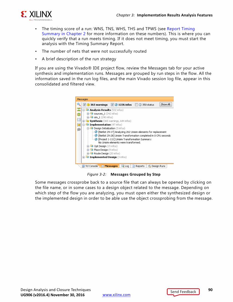
Design Analysis and Closure Techniques 90UG906 (v2016.3) October 5, 2016 www.xilinx.com
Chapter 3: Implementation Results Analysis Features
• The timing score of a run: WNS, TNS, WHS, THS and TPWS (see Report Timing Summary in Chapter 2 for more information on these numbers). This is where you can quickly verify that a run meets timing. If it does not meet timing, you must start the analysis with the Timing Summary Report.
• The number of nets that were not successfully routed
• A brief description of the run strategy
If you are using the Vivado® IDE project flow, review the Messages tab for your active synthesis and implementation runs. Messages are grouped by run steps in the flow. All the information saved in the run log files, and the main Vivado session log file, appear in this consolidated and filtered view.
Some messages crossprobe back to a source file that can always be opened by clicking on the file name, or in some cases to a design object related to the message. Depending on which step of the flow you are analyzing, you must open either the synthesized design or the implemented design in order to be able use the object crossprobing from the message.
X-Ref Target - Figure 3-2
Figure 3-2: Messages Grouped by Step
Send FeedbackUG906 (v2016.4) November 30, 2016

Design Analysis and Closure Techniques 91UG906 (v2016.3) October 5, 2016 www.xilinx.com
Chapter 3: Implementation Results Analysis Features
Placement AnalysisThis section discusses Placement Analysis and includes:
• Highlighting Placement
• Showing Connectivity
• Viewing Metrics
Highlighting PlacementAnother way to review design placement is to analyze cell placement. The Highlight Leaf Cells command helps in this analysis.
1. In the Netlist Window, select the levels of hierarchy to analyze.
2. From the popup menu, select Highlight Leaf Cells > Select a color.
3. If you select multiple levels of hierarchy, select Cycle Colors.
The leaf cells that make up the hierarchical cells are color coded in the Device window.
Send FeedbackUG906 (v2016.4) November 30, 2016
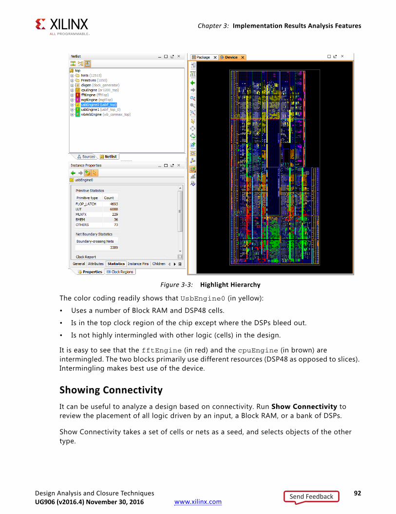
Design Analysis and Closure Techniques 92UG906 (v2016.3) October 5, 2016 www.xilinx.com
Chapter 3: Implementation Results Analysis Features
The color coding readily shows that UsbEngine0 (in yellow):
• Uses a number of Block RAM and DSP48 cells.
• Is in the top clock region of the chip except where the DSPs bleed out.
• Is not highly intermingled with other logic (cells) in the design.
It is easy to see that the fftEngine (in red) and the cpuEngine (in brown) are intermingled. The two blocks primarily use different resources (DSP48 as opposed to slices). Intermingling makes best use of the device.
Showing ConnectivityIt can be useful to analyze a design based on connectivity. Run Show Connectivity to review the placement of all logic driven by an input, a Block RAM, or a bank of DSPs.
Show Connectivity takes a set of cells or nets as a seed, and selects objects of the other type.
X-Ref Target - Figure 3-3
Figure 3-3: Highlight Hierarchy
Send FeedbackUG906 (v2016.4) November 30, 2016

Design Analysis and Closure Techniques 93UG906 (v2016.3) October 5, 2016 www.xilinx.com
Chapter 3: Implementation Results Analysis Features
TIP: Use this technique to build up and see cones of logic inside the design.
Figure 3-4 shows a Block RAM driving logic inside the device including OBUFs. A synthesis pragma stops synthesis from placing the output flop in the Block RAM during memory inferencing.
X-Ref Target - Figure 3-4
Figure 3-4: Show Connectivity
Send FeedbackUG906 (v2016.4) November 30, 2016
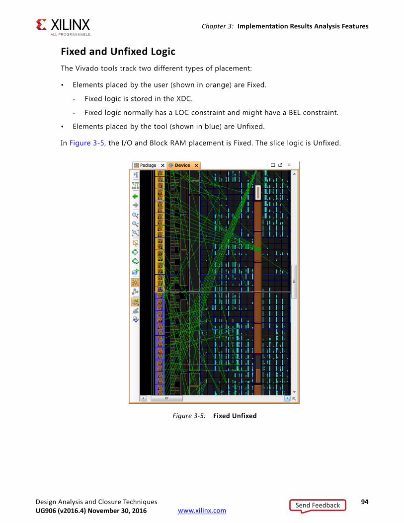
Design Analysis and Closure Techniques 94UG906 (v2016.3) October 5, 2016 www.xilinx.com
Chapter 3: Implementation Results Analysis Features
Fixed and Unfixed LogicThe Vivado tools track two different types of placement:
• Elements placed by the user (shown in orange) are Fixed.
° Fixed logic is stored in the XDC.
° Fixed logic normally has a LOC constraint and might have a BEL constraint.
• Elements placed by the tool (shown in blue) are Unfixed.
In Figure 3-5, the I/O and Block RAM placement is Fixed. The slice logic is Unfixed.
X-Ref Target - Figure 3-5
Figure 3-5: Fixed Unfixed
Send FeedbackUG906 (v2016.4) November 30, 2016

Design Analysis and Closure Techniques 95UG906 (v2016.3) October 5, 2016 www.xilinx.com
Chapter 3: Implementation Results Analysis Features
Cross ProbingFor designs synthesized with Vivado Synthesis, it is possible to cross probe back to the source files once the netlist design is in memory.
To cross probe:
1. Select the gate.
2. Select Go to Source from the popup menu, shown in the following figure.
Use cross probing to determine which source is involved in netlist gates. Due to the nature of synthesis transforms, it is not possible to cross probe back to source for every gate in the design.
X-Ref Target - Figure 3-6
Figure 3-6: Cross Probe Back To Source
Send FeedbackUG906 (v2016.4) November 30, 2016

Design Analysis and Closure Techniques 96UG906 (v2016.3) October 5, 2016 www.xilinx.com
Chapter 3: Implementation Results Analysis Features
Viewing MetricsAfter implementation finishes, you may want to analyze the design to see how it interacts with the device. The Vivado IDE has a number of metrics to help you determine logic and routing usage inside the device. The Metrics color code the device window based on a specified rule. To view a metric, right-click in the device view, select Metric, and then select the metric you would like to view. See the following figure.
X-Ref Target - Figure 3-7
Figure 3-7: Metrics
Send FeedbackUG906 (v2016.4) November 30, 2016

Design Analysis and Closure Techniques 97UG906 (v2016.3) October 5, 2016 www.xilinx.com
Chapter 3: Implementation Results Analysis Features
Metrics Requiring a Placed DesignFour metrics require a placed design in order to be accurate. They do not require a fully routed design.
• LUT Utilization per CLB: Color codes slices based on placed LUT utilization.
• FF Utilization per CLB: Color codes slices based on placed FF utilization.
• Vertical Routing Congestion per CLB: Color codes the fabric based on a best case estimate of vertical routing usage.
• Horizontal Routing Congestion per CLB: Color codes the fabric based on a best case estimate of horizontal routing usage.
Metrics in a Netlist Design with No PlacementTwo metrics are applicable if there are Pblocks. They do not depend on placement.
• LUT Utilization per Pblock: Color codes the Pblock based on an estimate of how the LUTs will be placed into the slices contained in the Pblock.
• FF Utilization per Pblock: Color codes the Pblock based on an estimate of how the FFs will be packed into the slices contained in the Pblock.
More than one rule can be used at a time as shown in Figure 3-7. Both LUT Utilization per CLB and FF Utilization per CLB are on.
TIP: If there are sections of the design with high utilization or high estimates of routing congestion, consider tweaking the RTL or placement constraints to reduce logic and routing utilization in that area.
Send FeedbackUG906 (v2016.4) November 30, 2016
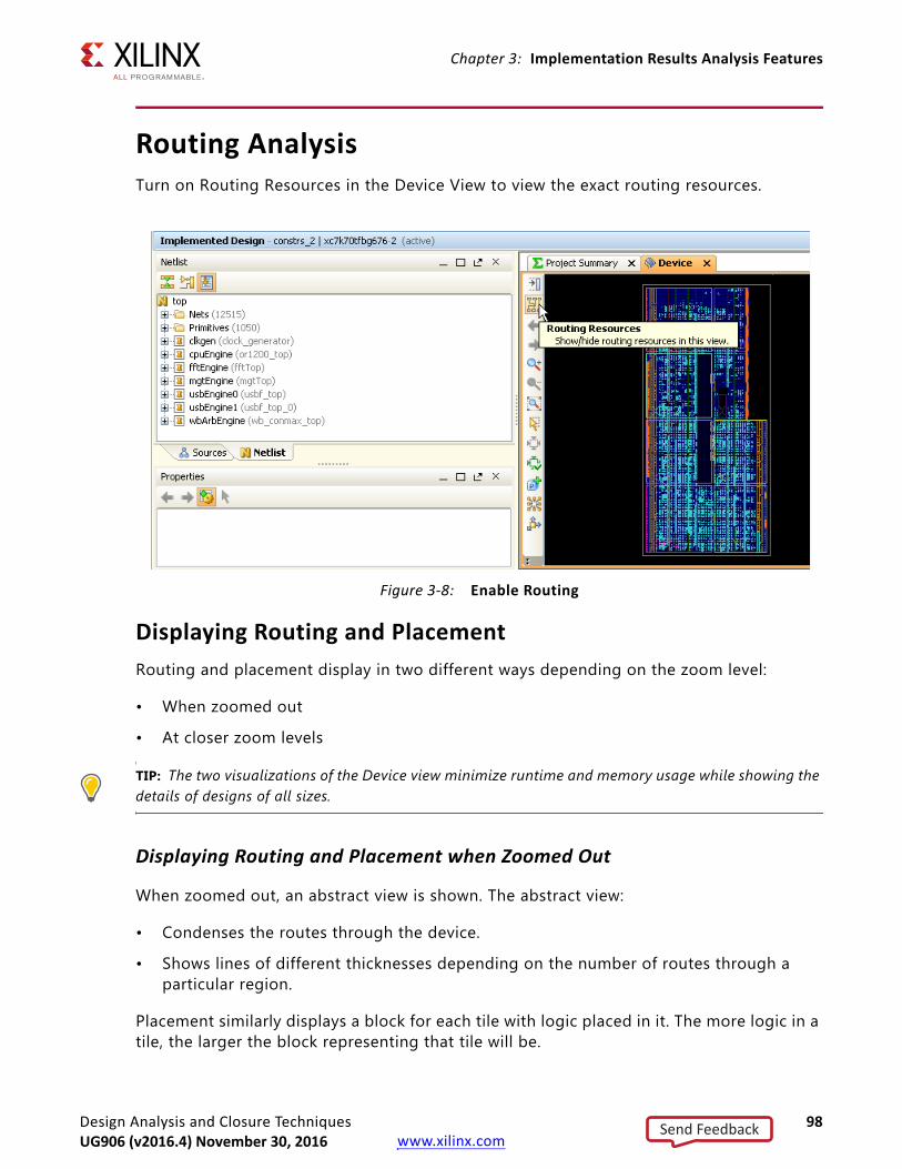
Design Analysis and Closure Techniques 98UG906 (v2016.3) October 5, 2016 www.xilinx.com
Chapter 3: Implementation Results Analysis Features
Routing AnalysisTurn on Routing Resources in the Device View to view the exact routing resources.
Displaying Routing and PlacementRouting and placement display in two different ways depending on the zoom level:
• When zoomed out
• At closer zoom levels
TIP: The two visualizations of the Device view minimize runtime and memory usage while showing the details of designs of all sizes.
Displaying Routing and Placement when Zoomed Out
When zoomed out, an abstract view is shown. The abstract view:
• Condenses the routes through the device.
• Shows lines of different thicknesses depending on the number of routes through a particular region.
Placement similarly displays a block for each tile with logic placed in it. The more logic in a tile, the larger the block representing that tile will be.
X-Ref Target - Figure 3-8
Figure 3-8: Enable Routing
Send FeedbackUG906 (v2016.4) November 30, 2016

Design Analysis and Closure Techniques 99UG906 (v2016.3) October 5, 2016 www.xilinx.com
Chapter 3: Implementation Results Analysis Features
Displaying Routing and Placement at Closer Zoom Levels
At closer zoom levels, the actual logic cells and routes show.
Viewing OptionsThe Device View is customizable to show the device, and design, in a variety of ways. Most of these are controlled through the Device View Options slideout.
X-Ref Target - Figure 3-9
Figure 3-9: Abstract View
X-Ref Target - Figure 3-10
Figure 3-10: Detailed View
Send FeedbackUG906 (v2016.4) November 30, 2016

Design Analysis and Closure Techniques 100UG906 (v2016.3) October 5, 2016 www.xilinx.com
Chapter 3: Implementation Results Analysis Features
You can enable or disable the graphics for different design and device resources, as well as modify the display colors.
Navigating in the Device View
X-Ref Target - Figure 3-11
Figure 3-11: Device View Layers
X-Ref Target - Figure 3-12
Figure 3-12: Navigating the Device View
Send FeedbackUG906 (v2016.4) November 30, 2016
Design Analysis and Closure Techniques 101UG906 (v2016.3) October 5, 2016 www.xilinx.com
Chapter 3: Implementation Results Analysis Features
Use the following tools to navigate in the Device View.
• Zoom Controls: Standard Zoom In, Zoom Out, and Zoom Full tools.
• Autofit Selection: Automatically zoom and pan to an object selected in any view outside of the device. Autofit Selection is particularly useful for cross probing.
• World View: The World View shows where the currently visible portion of the device is on the overall device. You can move and resize the World View, as well as drag and resize the yellow box to zoom and pan.
• Control Hotkey: Press Ctrl while clicking and dragging to pan the view.
Report Design AnalysisThe Design Analysis report provides information on timing path characteristics, design interconnect complexity, and congestion. You can use this information to make design or constraint changes that improve QoR and possibly alleviate routing congestion.
Running Report Design AnalysisYou can run Report Design Analysis from the Tcl console or the Vivado IDE. Report Design Analysis generates three categories of reports:
• Timing: reports timing and physical characteristics of timing paths
• Complexity: analyzes the design for routing complexity and LUT distribution
• Congestion: analyzes the design for routing congestion
To run Report Design Analysis in the Vivado IDE, select Tools > Report > Report Design Analysis.
Equivalent Tcl command: report_design_analysis -name design_analysis_1
Note: There are some Report Design Analysis options that are only available when running the report_design_analysis Tcl command. You can use the -name option to view the results of this Tcl command in the GUI.
Send FeedbackUG906 (v2016.4) November 30, 2016

Design Analysis and Closure Techniques 102UG906 (v2016.3) October 5, 2016 www.xilinx.com
Chapter 3: Implementation Results Analysis Features
In the Vivado IDE, the Report Design Analysis dialog box (shown in Figure 3-13) includes the following:
• Results Name Field
• Options Tab
• Advanced Tab
• Timer Settings Tab
Results Name Field
In the Results Name field at the top of the Report Design Analysis dialog box, specify the name of the graphical window for the report.
Equivalent Tcl option: -name <windowName>
X-Ref Target - Figure 3-13
Figure 3-13: Report Design Analysis Dialog Box
Send FeedbackUG906 (v2016.4) November 30, 2016

Design Analysis and Closure Techniques 103UG906 (v2016.3) October 5, 2016 www.xilinx.com
Chapter 3: Implementation Results Analysis Features
Options Tab
In the options tab (shown in Figure 3-13), the following fields are available:
• Timing
• Complexity
• Congestion
Timing Field
The Timing field allows you to report timing and physical characteristics of timing paths.
Equivalent Tcl option: -timing
You have the option to generate reports for all paths or specific timing paths. If you select the All Paths option you can specify the path delay type: max for setup, min for hold or min_max for setup and hold.
Equivalent Tcl option: -setup/-hold
You can also specify the maximum number of paths per clock group (default is 10).
Equivalent Tcl option: -max_paths <arg>
When you select the Specific Paths option, analysis is performed on the specified path objects. Click the Browse button (on the right) to open a search dialog box to aid in finding path objects. For more information about get_timing_paths, refer to this link in the Vivado Design Suite Tcl Command Reference Guide (UG835) [Ref 3].
Equivalent Tcl option: -of_timing_paths <args>
Select the Extend Analysis option to perform an extended analysis for each path of interest by also reporting the worst path to the startpoint and the worst path from the endpoint.
Equivalent Tcl option: -extend
Note: When running the Extend Analysis option (Tcl option -extend) for hold path analysis, the tool generates a report showing the setup and hold characteristics of the paths with the same start and endpoints to show if hold fixing is impacting setup timing.
Include logic-level distribution information by selecting that option and specifying the number of paths to be used. If you are also analyzing all paths, the number of paths selected overrides the maximum number of paths per clock group. If you are analyzing specific paths, logic-level distribution information is limited to the specified paths.
Equivalent Tcl option: -logic_level_distribution -logic_level_dist_paths <arg>
Send FeedbackUG906 (v2016.4) November 30, 2016

Design Analysis and Closure Techniques 104UG906 (v2016.3) October 5, 2016 www.xilinx.com
Chapter 3: Implementation Results Analysis Features
Complexity Field
The Complexity field allows you to report the complexity of the design netlist.
Equivalent Tcl option: -complexity
Select the Cells to Analyze option to specify the hierarchical cells to use for the complexity analysis. Click the Browse button (on the right) to open a search dialog box to aid in finding cell objects.
Equivalent Tcl option: -cells <args>
When you select the Hierarchical Depths option, you can select the levels of hierarchy to examine at the top level by default or at the level of the cells specified by the -cells option.
Equivalent Tcl option: -hierarchical_depth <arg>
Congestion Field
The Congestion field toggles the -congestion Tcl switch on and off.
Advanced Tab
In the Advanced tab (Figure 3-14), the following fields are available:
• File Output
• Miscellaneous
File Output Field
You can write the results to a file in addition to generating a GUI report by selecting Write results to file and specifying a file name in the field to the right. Click the Browse button to select a different directory.
Equivalent Tcl option: -file <arg>
Select the Overwrite option to overwrite an existing file with the new analysis results.
Select Append to append the new results.
Equivalent Tcl option: -append
Miscellaneous Field
The Miscellaneous field provides options to ignore command errors and suspend message limits during command execution.
Equivalent Tcl option: -quiet -verbose
Send FeedbackUG906 (v2016.4) November 30, 2016

Design Analysis and Closure Techniques 105UG906 (v2016.3) October 5, 2016 www.xilinx.com
Chapter 3: Implementation Results Analysis Features
Timer Settings Tab
In the timer settings tab (shown in Figure 3-15), the following fields and options are available.
• Interconnect Option
• Speed Grade Option
• Multi-Corner Configuration Field
• Disable Flight Delays Option
X-Ref Target - Figure 3-14
Figure 3-14: Report Design Analysis Dialog Box, Advanced Tab
Send FeedbackUG906 (v2016.4) November 30, 2016

Design Analysis and Closure Techniques 106UG906 (v2016.3) October 5, 2016 www.xilinx.com
Chapter 3: Implementation Results Analysis Features
Interconnect Option
You can select the interconnect model to be used in your analysis of timing paths:
• actual provides the most accurate delays for a routed design.
• estimated includes an estimate of the interconnect delays based on the placement and connectivity of the design onto the device prior to implementation. Estimated delay can be specified even if the design is fully routed.
• none includes no interconnect delay in the timing analysis; only the logic delay is applied.
Equivalent Tcl command: set_delay_model -interconnect <arg>
For more information about set_delay_model, refer to the Vivado Design Suite Tcl Command Reference Guide (UG835) [Ref 3].
Speed Grade Option
You can perform analysis on the default speed grade or select a different speed grade for analysis.
Equivalent Tcl command: set_speed_grade <arg>
For more information about set_speed_grade, refer to the Vivado Design Suite Tcl Command Reference Guide (UG835) [Ref 3].
Multi-Corner Configuration Field
You can limit the default four-corner analysis performed by the Vivado timing analysis engine, as appropriate, using the options available in this field.
Equivalent Tcl command: config_timing_corners -corner <arg> -delay_type <arg>
For more information about config_timing_corners, refer to the Vivado Design Suite Tcl Command Reference Guide (UG835) [Ref 3].
Disable Flight Delays Option
You can select this option to disable the addition of package delays to I/O timing calculations.
Equivalent Tcl command: config_timing_analysis -disable_flight_delays <arg>
For more information about config_timing_analysis, refer to the Vivado Design Suite Tcl Command Reference Guide (UG835) [Ref 3].
Send FeedbackUG906 (v2016.4) November 30, 2016

Design Analysis and Closure Techniques 107UG906 (v2016.3) October 5, 2016 www.xilinx.com
Chapter 3: Implementation Results Analysis Features
Command Line Only OptionsThe following Timing options are only available from the Tcl command line and can be used with the -name option to generate a GUI report.
• -routed_vs_estimated
This option reports the estimated versus actual routed delays side-by-side for the same path. Some fields within the Timing Category in the report are prefaced with "Estimated" or "Routed" for comparison.
• -return_timing_paths
• -end_point_clock
• -logic_levels
X-Ref Target - Figure 3-15
Figure 3-15: Report Design Analysis, Timer Settings Tab
Send FeedbackUG906 (v2016.4) November 30, 2016

Design Analysis and Closure Techniques 108UG906 (v2016.3) October 5, 2016 www.xilinx.com
Chapter 3: Implementation Results Analysis Features
The following Complexity options are only available from the command line and can be used with the -name option to generate a GUI report.
• -bounding boxes <arg>
This option performs the complexity analysis of the specified bounding boxes. For example:
-bounding_boxes { "CLE_M_X21Y239:CLEL_R_X28Y254" "CLEL_R_X18Y171:CLE_M_X26Y186" }
Note: A space is required between the open bracket `{` and the start of the bounding box, as shown in the previous example.
Timing Path Characteristics ReportThe following figure shows example output after running the Report Design Analysis in Timing Mode to show the path characteristics of only the 10 Worst Setup paths in the design. You can generate the report from the GUI (Tools > Report > Report Design Analysis) or using the Tcl command:
report_design_analysis -name <arg>
TIP: To create hold path characteristics, select Path delay type: min in the Options tab of the Report Design Analysis dialog box or add -hold to the Tcl command. For more information on Tcl command syntax, see the Vivado Design Suite Tcl Command Reference Guide (UG835) [Ref 3].
Report Design Analysis can also provide a Logic Level Distribution table for the worst timing paths. The default number of paths analyzed for the Logic Level Distribution table is 1,000 and can be changed in the Report Design Analysis dialog box. The Logic Level Distribution table is not generated by default but can be generated when you select the Include logic level distribution in the Report Design Analysis dialog box Options tab. An example of the Logic Level Distribution table is shown in the following figure.
X-Ref Target - Figure 3-16
Figure 3-16: Example Setup Path Characteristics
Send FeedbackUG906 (v2016.4) November 30, 2016

Design Analysis and Closure Techniques 109UG906 (v2016.3) October 5, 2016 www.xilinx.com
Chapter 3: Implementation Results Analysis Features
Analyzing Specific Paths
Figure 3-18 shows an example report from Report Design Analysis in Timing Mode with specific paths selected.
In this case, the Path Characteristics and the Logic Level Distribution tables (if selected) are limited to the specified path. To specify the paths, click the Browse button to the right of the Specific paths selection in the Report Design Analysis dialog box. This opens the Find Timing Paths dialog box (shown in Figure 3-19).
X-Ref Target - Figure 3-17
Figure 3-17: Example of Logic Level Distribution Report
X-Ref Target - Figure 3-18
Figure 3-18: Example of Specific Timing Path Characteristics
Send FeedbackUG906 (v2016.4) November 30, 2016

Design Analysis and Closure Techniques 110UG906 (v2016.3) October 5, 2016 www.xilinx.com
Chapter 3: Implementation Results Analysis Features
Analyzing the Worst Path along with Preceding and Following Worst Paths
The figure below shows an example report from Report Design Analysis in Timing Mode with the Extend analysis option selected.
Note: The Extend Analysis for All Paths option is currently only available for setup analysis.
The Path Characteristics are reported on the worst setup path along with the worst setup path to the startpoint cell (PrePath) and the worst setup path from the endpoint cell (PostPath). The -extend option incurs higher runtime as several timing analyses are required to collect the characteristics of all reported paths.
Equivalent Tcl Command: report_design_analysis -extend
X-Ref Target - Figure 3-19
Figure 3-19: Find Timing Paths Dialog Box
X-Ref Target - Figure 3-20
Figure 3-20: Extended Path Characteristics of the Worst Setup Path
Send FeedbackUG906 (v2016.4) November 30, 2016

Design Analysis and Closure Techniques 111UG906 (v2016.3) October 5, 2016 www.xilinx.com
Chapter 3: Implementation Results Analysis Features
Reading and Interpreting Timing Path Characteristics Reports
The path characteristics fall into four main categories: timing, logic, physical, and property. You can find the definition of each characteristics in the command long help.
Tcl Command: report_design_analysis -help
Alternatively, you can find the same information in the Vivado Design Suite Tcl Command Reference Guide (UG835) [Ref 3].
Category 1: Timing
• Timing Analysis: The Path Type and Requirement detail the timing analysis type (SETUP or HOLD) along with the timing path requirement. The Slack indicates whether or not the timing path requirement is met based on the timing analysis as dictated by the timing constraints. The Timing Exception indicates if any timing exceptions such as multicycle path or max delay have been applied to the timing path.
Checking the path requirement is often the first step in debugging missing or incorrect timing constraints:
° Paths with setup requirement under 4 ns must be reviewed to verify their validity in the design, especially for clock domain crossing paths.
° Paths with setup requirement under 2 ns are difficult to meet and must be avoided in general, especially for the older architectures.
° In general, when small setup requirements are present, check for missing timing exception constraints and also check the source and destination clock edges. The timing analysis always assumes the smallest positive difference between source and destination clock edges unless overridden by a timing exception constraint.
° Positive hold path requirements need to be reviewed as they are not common and are difficult to meet. When positive hold path requirements are present, check for missing multicycle path constraints for hold analysis that might have only been applied to the path for setup analysis. Also check the relationship between source and destination clocks for correctness.
• Datapath: The Path Delay, Logic Delay, and Net Delay detail the total datapath delay along with its breakdown into delay contribution by logic cells and nets.
° If the Logic Delay makes up an unusually high proportion of the total datapath delay, for example 50% or higher, it is advised to examine the datapath logic depth and types of cells on the logic path, and possibly modify the RTL or synthesis options to reduce the path depth or use cells with faster delays.
° If the Net Delay dominates the total path delay for a setup path where the Requirement is reasonable, it is advised to analyze some of the physical characteristics and property characteristics of the path listed in this section. Specific items to look at include the High Fanout and Cumulative Fanout
Send FeedbackUG906 (v2016.4) November 30, 2016

Design Analysis and Closure Techniques 112UG906 (v2016.3) October 5, 2016 www.xilinx.com
Chapter 3: Implementation Results Analysis Features
characteristics to understand if some nets of the path have a high fanout that could potentially be causing a placement problem. Also check the Hold Fix Detour characteristic to understand if hold fixing has occurred on the path (this characteristic is only updated when report_design_analysis is run in the same session as route_design, and not after loading a post-route checkpoint).
IMPORTANT: The LUT input pins have different delay characteristics. The physical pins (or site pins) of higher index are faster than the pins of lower index. Be aware of the difference in 7 series and UltraScale™ device LUT delay reporting. In 7 Series devices, the variable portion of LUT delay is reported as part of the net delay in front of the LUT. In UltraScale devices, the variable portion of LUT delay is reported as logic delay. Therefore, the 7 Series device Net Delay/Logic Delay ratio will be larger than the ratio for UltraScale devices.
• Clocks: The Start Point Clock, End Point Clock, Clock Relationship, and Clock Skew detail information regarding the timing path clocks. The Start Point Clock and Endpoint Clock list the respective source clock and destination clock for the timing path.
° Check that the Clock Relationship is correct and expected. For intra-clock paths or synchronous clock domain crossing paths, the relationship is labeled as "Safely Timed." You must verify that the Requirement and Clock Skew are reasonable. For asynchronous clocks, the relationship is labeled as "No Common Primary Clock" or "No Common Period." Asynchronous clock domain crossing paths must be covered by timing exceptions (check the Timing Exception value).
° Check that the Clock Skew is reasonable. When analyzing clock skew, check the clock tree structure for cascaded clock buffers. In 7 Series devices, check for different clock buffer types for the source and destination clocks. In UltraScale devices, it might be necessary to examine the placement and routing of the clock nets because it depends on logic loads placement. The crossing of a Clock Region boundary or an I/O Column can result in higher clock skew; this is expected.
Note that almost all of the Timing Characteristics provided by report_design_analysis are available in a timing report.
Send FeedbackUG906 (v2016.4) November 30, 2016

Design Analysis and Closure Techniques 113UG906 (v2016.3) October 5, 2016 www.xilinx.com
Chapter 3: Implementation Results Analysis Features
Category 2: Logic
• Path: The Start Point Pin Primitive, End Point Pin Primitive, Start Point Pin, End Point Pin, Logic Levels, Logical Path, and Comb DSP logic characteristics provide some basic information about the timing path.
° The Start Point Pin Primitive and End Point Pin Primitive are the reference pin names of the timing path start point and end point. Check that the Start Point Pin Primitive and End Point Pin Primitive are expected timing path start and endpoints. The Start Point Pin and End Point Pin identify the actual timing path pin startpoints and endpoints that would show in the header of a typical timing report.
Check for endpoint pins such as CLR, PRE, RST, and CE that could potentially be part of high-fanout nets for control signals such as asynchronous resets and clock enable signals. Also check the type of cell, because some primitives like block RAMs and DSPs have larger Clock-to-Q delay and setup/hold requirements than other cells. Their presence in the path can potentially consume a significant portion of the path timing budget.
° The Logic Levels and Logical Path detail the number of logic levels and the types of primitives in the datapath. You can use this information to quickly check if a high number of logic levels is mostly due to LUTs or to a mix of LUT/CARRY/MUXF cells. CARRY and MUXF cells are usually connected to nets with dedicated routes that have null or very small delays, while LUT inputs always need to be routed through the fabric.
When the path mostly contains LUTs, it is also important to check their size. Try to understand why there are several smaller LUTs (non-LUT6) that are chained and what prevents synthesis from targeting LUT6 only, which can reduce the logic levels. There can be properties like KEEP/DONT_TOUCH/MARK_DEBUG or mid-to-high fanout nets in the path that also impact mapping efficiency.
Based on the outcome of your analysis, you can either modify the RTL source, add/modify attributes in the RTL, or use different synthesis settings to reduce the number of LUTs on the path. Also, you can use the option -remap of the opt_design command to re-optimize LUT mapping and possibly eliminate some smaller LUTs.
° The COMB DSP details the number of DSPs used as combinatorial logic that are part of the datapath.
• Cells: DOA_REG, DOB_REG, MREG, PREG correspond to Block RAMs and DSPs optional register properties. Timing is more difficult to meet on paths from RAMBs or DSPs with no output registers and with several logic levels. You should consider modifying your design to use the RAMB or DSP output registers if these paths are having difficulty meeting the timing requirements.
Send FeedbackUG906 (v2016.4) November 30, 2016
Design Analysis and Closure Techniques 114UG906 (v2016.3) October 5, 2016 www.xilinx.com
Chapter 3: Implementation Results Analysis Features
Category 3: Physical
• Architectural Boundary Crossings: The BRAM Crossings, DSP Crossings, IO Crossings, Config Crossings, and SLR Crossings identify whether the path is crossing architectural resources such as BRAM columns, DSP columns, IO Columns, CONFIG Block Columns, or SLR boundaries.
The crossing of many architectural columns does not always represent a problem. Check for high net delay or large skew in conjunction with the crossing of many architectural columns. If many architectural column crossings appear to be the cause of timing issues across multiple implementation runs for a particular module, consider minimal floorplanning using Pblocks to reduce the crossings of the architectural column(s) or SLR boundary.
• Path Placement Restrictions: Pblocks. Excessive floorplanning can sometimes prevent the tool from achieving the optimal results. Paths that cross multiple Pblocks can sometimes experience timing issues.
° If the path crosses multiple Pblocks, examine the location of the Pblocks and the impact on the timing path placement.
° If the Pblocks are adjacent, consider creating a single Pblock that is a super-set of each individual Pblock. This could potentially improve timing by being less restrictive on the placer.
If physical requirements dictate that the Pblocks are placed far apart, consider pipelining between the Pblocks to help meet timing requirements.
• Placement Box: Bounding Box Size, Clock Region Distance, Combined LUT Pairs
° If the Bounding Box Size or Clock Region Distance of the timing path is too large, try using directives in place_design. In UltraScale devices, be especially aware of the Clock Region Distance and its possible impact on timing path Clock Skew.
• Net Fanout and Detour:
° High Fanout shows the highest fanout of all nets in the datapath, and Cumulative Fanout corresponds to the sum of all datapath net fanouts.
If High Fanout and Cumulative Fanout are large, the timing violations are very likely due to the fanout impact on routing and net delay.
If physical optimization was run and did not reduce the fanout, check for MARK_DEBUG and DONT_TOUCH constraints preventing replication.
If replication is desired on the net prior to implementation, you can use the MAX_FANOUT constraint in synthesis, either inside the RTL or in an XDC file. Due to reliance on placement for good timing for high fanout nets, it is usually not
Send FeedbackUG906 (v2016.4) November 30, 2016
Design Analysis and Closure Techniques 115UG906 (v2016.3) October 5, 2016 www.xilinx.com
Chapter 3: Implementation Results Analysis Features
recommended to have synthesis perform replication and it is best to rely on post-placement physical optimization (phys_opt_design) for replication. You can also increase the physical optimization effort to also optimize paths with a small positive slack by using different directives such as Explore, AggressiveExplore, or AggressiveFanoutOpt.
If fanout reduction is desired on a specific net during implementation, you can force the replication using the command:phy_opt_design -force_replication_on_nets <netName>
° When the Hold Fix Detour is asserted, the routing on the datapath was delayed in order to meet the path hold time requirement. If the path is failing setup, check for excessive skew between the Source and Destination clocks. Also check for proper timing constraints between the Source and Destination clocks in case the hold path requirement is positive (it should be zero or negative in most common cases).
Category 4: Property
• LUT Combining: Combined LUT Pairs indicates that there are combined LUT pairs present in the path. While combining LUT pairs can reduce logic utilization, it can also restrict the placement solutions and can create congestion due to high pin density. If LUT combining appears to be an issue in the design, it is recommended to disable LUT combining in synthesis by using the -no_lc option.
• Optimization Blocking: Mark Debug and Dont Touch can quickly identify whether there are any nets or cells in the path that the tool is not allowed optimize.
° The default behavior of setting the MARK_DEBUG property is to also to set the DONT_TOUCH property. Consider setting DONT_TOUCH to FALSE to allow for optimization.
° DONT_TOUCH disables optimizations such as cell or net replication. Evaluate the need for DONT_TOUCH constraints and remove them if possible. When a net enters a hierarchical cell with DONT_TOUCH, the portion of the net inside the hierarchical cell cannot be replicated. If DONT_TOUCH is used to prevent logic trimming, check the design for correctness. One simple example would be logic removed due to unconnected outputs.
Send FeedbackUG906 (v2016.4) November 30, 2016

Design Analysis and Closure Techniques 116UG906 (v2016.3) October 5, 2016 www.xilinx.com
Chapter 3: Implementation Results Analysis Features
• Fixed Placement and Routing: The Fixed Loc, Fixed Route can quickly identify whether there are any fixed placement or fixed routing constraints that might be impacting the timing path slack.
° Using cell location constraints can help stabilizing QoR for a difficult design. If timing can no longer be met after modifying the design, you can try removing the placement constraints to give more flexibility to the placer.
° Having fixed routes prevents the router from optimizing the net delays to meet timing. A timing path with locked routing usually shares nets with other paths that can be negatively impacted by this constraint. Use fixed routes only when necessary and when it does not affect interacting paths.
° Always be aware that changes to other physical constraints such as Pblocks might require the fixed cell locations or fixed routes to also be updated.
Complexity ReportThe complexity report shows the Rent Exponent, Average Fanout, and distribution of the types of leaf cells of the top-level design and/or of hierarchical cells that contain more than 1000 leaf cells. The Rent exponent is the relationship between the number of ports and the number of cells of a netlist partition when recursively partitioning the design with a min-cut algorithm. It is computed with similar algorithms as the ones used by the placer during global placement. Therefore it can provide a good indication of the challenges seen by the placer, especially when the hierarchy of the design matches well the physical partitions found during global placement.
The Rent Exponent is defined by the Rent's rule:
ports = constant x cellsRent
log(ports) = Rent x log(cells) + constant
A design with higher Rent exponent corresponds to a design where the groups of highly connected logic also have strong connectivity with other groups. This usually translates into a higher utilization of global routing resources and an increased routing complexity. The Rent exponent provided in this report is computed on the unplaced and unrouted netlist.
After placement, the Rent exponent of the same design can differ as it is based on physical partitions instead of logical partitions. The post-placement Rent exponent is not reported by the Report Design Analysis command as it is recommended to analyze the congestion reports once the design is placed instead.
Report Design Analysis runs in Complexity Mode when you do either of the following:
• Check the Complexity option in the Report Design Analysis dialog box Options tab.
• Execute the report_design_analysis TCL command and use any of the options shown in the following table.
Send FeedbackUG906 (v2016.4) November 30, 2016

Design Analysis and Closure Techniques 117UG906 (v2016.3) October 5, 2016 www.xilinx.com
Chapter 3: Implementation Results Analysis Features
Analyzing the Design Complexity at the Top Level
The following figure shows an example report from Report Design Analysis in Complexity Mode that reports up to one level of hierarchy from the top module.
Tcl Command:
report_design_analysis -complexity -hierarchical_depth 1
Reading and Interpreting a Complexity Report
The Complexity Characteristics table from the previous example shows the Rent exponent and average fanout for each level of hierarchy below the top level. The typical ranges to consider when reviewing these metrics are the following:
• Rent exponent:
° Between 0.0 and 0.65: The complexity is considered low to normal and does not highlight any potential problems.
° Between 0.65 and 0.85: The complexity is considered high, especially when the total number of instances is above 25k.
° Above 0.85: The complexity is very high, and if the number of instances is also high, the design can potentially fail during implementation.
Table 3-1: Options that Run Report Design Analysis in Complexity Mode
Tcl Option Description
-complexity Must be specified to run the report design analysis in Complexity Mode.
-cells <arg> Specifies the hierarchical cells to use when analyzing the complexity.
-hierarchical_depth <arg> The levels of hierarchy to examine at the top level by default or at the level of the cells specified by the -cells option.
X-Ref Target - Figure 3-21
Figure 3-21: Complexity Analysis at the Top Level and Hierarchical Depth of 1
Send FeedbackUG906 (v2016.4) November 30, 2016

Design Analysis and Closure Techniques 118UG906 (v2016.3) October 5, 2016 www.xilinx.com
Chapter 3: Implementation Results Analysis Features
• Average fanout:
° Below 4: It is considered normal.
° Between 4 and 5: The implementation tools can show difficulty to place the design without congestion. In the case of a SSI device, if the total number of instances is above 100k, the placer can have problems finding a placement solution that fits in 1 SLR or that is spread over 2 SLRs.
° Above 5: The design can potentially fail during implementation.
You must treat high Rent exponents and/or high average fanouts for larger modules with higher importance. Smaller modules, especially under 10k total instances, can have higher Rent exponent and average fanout, and yet be simple to place and route successfully. For this reason, the Total Instances column must always be reviewed along with the Rent exponent and average fanout.
The complexity characteristics might not always predict routing congestion. Other factors such as I/O location constraints, floorplanning, and macro primitive location in the target device can limit the placement solution space and introduce congestion. The effect of such constraints is better analyzed by the congestion reports available after placement.
Other items to consider when interpreting the Complexity Characteristics table:
• A higher percentage of LUT6s in a module usually increases the average fanout and potentially the Rent exponent.
• A high number of RAMB and DSPs can increase the Rent exponent because these primitives have a large amount of connectivity.
• The hierarchical instances with higher Rent exponents or higher average fanouts are not always a problem because the placer operates on a flat netlist and can break these instances into easier groups of logic to place. This report provides an indication of where a netlist problem can possibly exist if a module stands out clearly.
When a large module exhibits a high Rent exponent and/or average fanout that is causing congestion and timing issues, consider the following actions:
° Reduce the connectivity of the module. Preserving the hierarchy to prevent cross-boundary optimization in synthesis can reduce the use of LUT6s and consequently reduce the netlist density.
° Try to disable LUT combining in synthesis.
° Use a Congestion Strategy during Implementation or SpreadLogic placement directive that can potentially help to relieve congestion. If the design is targeting an SSI Device, consider trying several SSI placement directives.
° Use simple floorplanning at the SLR level for SSI devices, or at the clock region level in general, to keep congested groups of logic separate, or to guide global placement towards a solution similar to a previously found good placement.
Send FeedbackUG906 (v2016.4) November 30, 2016

Design Analysis and Closure Techniques 119UG906 (v2016.3) October 5, 2016 www.xilinx.com
Chapter 3: Implementation Results Analysis Features
Congestion ReportThe Congestion reports show the congested areas of the device and the name of design modules present in these areas. Congestion can potentially lead to timing closure issues if the critical paths are placed inside or next to a congested area.
Analyzing the Design Congestion
To run Report Design Analysis in Congestion Mode, the Congestion option must be specified in the Options tab of the Report Design Analysis dialog box, and the design must be placed and/or routed. Running Report Design Analysis with Congestion Mode on an unplaced design results in nothing being reported.
Report Design Analysis produces six congestion tables:
• Placed Maximum Level Congestion Reporting
• Average Initial Router Maximum Congestion Reporting
• Router Maximum Level Congestion Reporting
• SLR Net Crossing Reporting
• Placed Tile Based Congestion Metric (Vertical)
• Placed Tile Based Congestion Metric (Horizontal)
Maximum Congestion Reports
These tables report all the windows with the same maximum congestion level (window size) seen in a particular direction. The columns are defined as follows:
° Direction: The direction of the congested routing resources (North, South, West, or East)
° Window Size: The Window Size of the congestion in CLB tiles.
° Congestion in Window (%): Indicates the estimated routing resource utilization in the defined window. This value can be greater than 100%.
° Rent: Indicates the Rent in the Window.
° Congestion Window: Indicates the bounding CLB tiles where the congestion for the identified Direction is present. The CLB coordinates correspond to the lower left and upper right corners of the window.
TIP: The Congestion Window column is only available in the text report. In the GUI report, you can select the congestion window, which highlights the congested area in the Device View.
Send FeedbackUG906 (v2016.4) November 30, 2016

Design Analysis and Closure Techniques 120UG906 (v2016.3) October 5, 2016 www.xilinx.com
Chapter 3: Implementation Results Analysis Features
° Cell Names: Indicates the parent instance that contains the hierarchical cells involved in the Congestion Window, up to the three largest contributors along with their contribution percentage.
TIP: In the GUI report, you can select the hyperlinked cell names to highlight the respective leaf cells in the congestion window.
° LUT usage %: The percentage of LUT utilization in the Window.
° Flop usage %: The percentage of FD (including LD) utilization in the Window.
° MUX usage %: The percentage of MUXF utilization in the Window.
° RAMB18 usage %: The percentage of RAMB18 utilization in the Window.
° RAMB36 usage %: The percentage of RAMB36 utilization in the Window.
° DSP usage %: The percentage of DSP utilization in the Window.
Placed Maximum Level Congestion Reporting
When analyzing the Placed Maximum Level Congestion Reporting Table of your design for Congestion and Timing QoR, look for the following:
° If a high level of LUT usage exists, examine the instances that have a high percentage of LUT6s in the Complexity report.
° In case of high RAMB or DSP utilization in the congested area, check for Pblock constraints that might be limiting the available placement area of the reported modules. Use various targeted placement directives to relieve congestion such as the BlockPlacement or SpreadLogic directives. In some cases, it might be beneficial to reuse the RAMB or DSP placement from a previous run that showed low congestion and resulted in good Timing QoR.
The following figure shows an example of the Placed Maximum Level Congestion Reporting table. Using this report, you can examine areas of the device defined by the Congestion window along with the modules residing in that window. The resource usage percentages gives an indication of the types of resources located in the congested area.
X-Ref Target - Figure 3-22
Figure 3-22: Example Placed Maximum Level Congestion Reporting Table
Send FeedbackUG906 (v2016.4) November 30, 2016
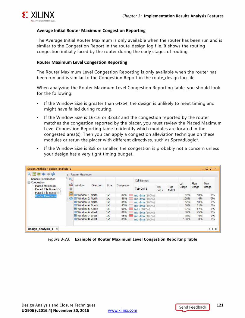
Design Analysis and Closure Techniques 121UG906 (v2016.3) October 5, 2016 www.xilinx.com
Chapter 3: Implementation Results Analysis Features
Average Initial Router Maximum Congestion Reporting
The Average Initial Router Maximum is only available when the router has been run and is similar to the Congestion Report in the route_design log file. It shows the routing congestion initially faced by the router during the early stages of routing.
Router Maximum Level Congestion Reporting
The Router Maximum Level Congestion Reporting is only available when the router has been run and is similar to the Congestion Report in the route_design log file.
When analyzing the Router Maximum Level Congestion Reporting table, you should look for the following:
• If the Window Size is greater than 64x64, the design is unlikely to meet timing and might have failed during routing.
• If the Window Size is 16x16 or 32x32 and the congestion reported by the router matches the congestion reported by the placer, you must review the Placed Maximum Level Congestion Reporting table to identify which modules are located in the congested area(s). Then you can apply a congestion alleviation technique on these modules or rerun the placer with different directives, such as SpreadLogic*.
• If the Window Size is 8x8 or smaller, the congestion is probably not a concern unless your design has a very tight timing budget.
X-Ref Target - Figure 3-23
Figure 3-23: Example of Router Maximum Level Congestion Reporting Table
Send FeedbackUG906 (v2016.4) November 30, 2016

Design Analysis and Closure Techniques 122UG906 (v2016.3) October 5, 2016 www.xilinx.com
Chapter 3: Implementation Results Analysis Features
SLR Net Crossing Reporting
The SLR Net Crossing Reporting is only applicable to SSI Devices and reports the number of nets contained in a module that cross the SLR boundaries. For each module, the table provides further details of which SLRs are crossed by the nets. The following figure shows an example of the SLR Net Crossing Reporting table.
Note: When a net has loads in multiple SLRs, it is only counted once for the furthest cut. For example, a net driven from SLR0 to loads in SLR1, SLR2, and SLR3 is only counted once under the 0-3 cuts, with SLR3 being the "furthest fanout" from SLR0. This counting method enables to sum the number of nets under each column (0-1 Cuts, 1-2 Cuts, and so on) to match to total number of nets crossing, as each net is only counted once.
When analyzing the SLR Net Crossing Reporting Table of your design for Congestion and Timing QoR, look for the following:
° When using SSI Devices, the SSI placement directives can be beneficial for both timing and congestion.
° If a particular module that is crossing SLRs is consistently experiencing timing issues across multiple implementation runs using various placement directives, attempt light Pblocking to constrain the module to a single SLR.
Placed Tile Based Congestion Metrics
The Placed Tile Based Congestion Metric reports the 10 CLB tiles with highest congestion, along with the modules that have cells located in the CLB tile. Figure 3-25 and Figure 3-26 show examples of the Placed Tile Based Congestion Metric for both Vertical and Horizontal routing.
° Tile Name: The CLB tile where the congestion is occurring.
° RPM Grid Column/Row: The RPM location of the CLB tile in the device.
° Congestion in Window (%): Indicates the percentage of estimated routing resource utilization through the CLB tile. This value can be greater than 100%.
X-Ref Target - Figure 3-24
Figure 3-24: Example SLR Net Crossing Reporting Table
Send FeedbackUG906 (v2016.4) November 30, 2016
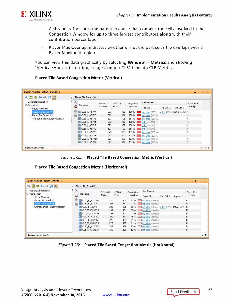
Design Analysis and Closure Techniques 123UG906 (v2016.3) October 5, 2016 www.xilinx.com
Chapter 3: Implementation Results Analysis Features
° Cell Names: Indicates the parent instance that contains the cells involved in the Congestion Window for up to three largest contributors along with their contribution percentage.
° Placer Max Overlap: indicates whether or not the particular tile overlaps with a Placer Maximum region.
You can view this data graphically by selecting Window > Metrics and showing "Vertical/Horizontal routing congestion per CLB" beneath CLB Metrics.
Placed Tile Based Congestion Metric (Vertical)
Placed Tile Based Congestion Metric (Horizontal)
X-Ref Target - Figure 3-25
Figure 3-25: Placed Tile Based Congestion Metric (Vertical)
X-Ref Target - Figure 3-26
Figure 3-26: Placed Tile Based Congestion Metric (Horizontal)
Send FeedbackUG906 (v2016.4) November 30, 2016

Design Analysis and Closure Techniques 124UG906 (v2016.3) October 5, 2016 www.xilinx.com
Chapter 4
Viewing Reports and Messages
Introduction to Reports and MessagesThe Xilinx® Vivado® Integrated Design Environment (IDE) generates reports and messages to inform you of the state of the design or design processes during various tool interactions. Reports are generated by you (or by the tool) at key steps in the design flow. The reports summarize specific information about the design.
The tool generates messages automatically at each step of the design process, and for many user actions.
Messages and reports are stored in the Messages and Reports windows in the Results window area.
When you run any of the following commands, the tool starts a new process:
• Run Synthesis
• Run Implementation
• launch_runs (Tcl)
For more information on Tcl commands, see the Vivado Design Suite Tcl Command Reference Guide (UG835) [Ref 3], or type <command> -help.
The process generates messages and reports that persist on disk until you reset the run. Messages that relate to a run appear when a project is open. The tool displays only the messages for the active run in the Messages window.
Reports result from a variety of actions in the Vivado IDE:
• When you load a design, many different reporting commands are available through the Tools menu.
• Running Synthesis or Implementation creates reports as part of the run.
Send FeedbackUG906 (v2016.4) November 30, 2016

Design Analysis and Closure Techniques 125UG906 (v2016.3) October 5, 2016 www.xilinx.com
Chapter 4: Viewing Reports and Messages
Viewing and Managing Messages in the IDEMessages provide brief status notes about specific elements of the design, or about errors that occurred in tool processes.
TIP: Review the messages to determine whether the Vivado tools are having difficulty, or are encountering errors in any sections of the design.
Using the Reports WindowThe reports for the active Synthesis and Implementation runs appear in the Reports window. Double click a report to view it in the text viewer. Select the Reports tab of the Run Properties window to view reports of the run selected in the Design Runs window.
Using the Messages WindowThere are two types of messages:
• Messages stored on disk
• Messages stored in memory
The Vivado Integrated Design Environment (IDE) groups messages in the Messages window by the action that created the message.
Use the command buttons on the toolbar menu to group the messages by message ID or file.
X-Ref Target - Figure 4-1
Figure 4-1: Reports Window
X-Ref Target - Figure 4-2
Figure 4-2: Messages Window
Send FeedbackUG906 (v2016.4) November 30, 2016
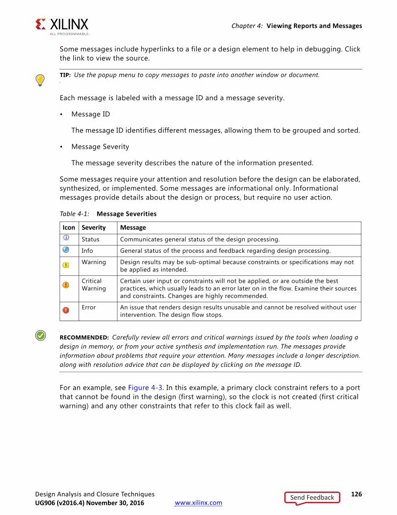
Design Analysis and Closure Techniques 126UG906 (v2016.3) October 5, 2016 www.xilinx.com
Chapter 4: Viewing Reports and Messages
Some messages include hyperlinks to a file or a design element to help in debugging. Click the link to view the source.
TIP: Use the popup menu to copy messages to paste into another window or document.
Each message is labeled with a message ID and a message severity.
• Message ID
The message ID identifies different messages, allowing them to be grouped and sorted.
• Message Severity
The message severity describes the nature of the information presented.
Some messages require your attention and resolution before the design can be elaborated, synthesized, or implemented. Some messages are informational only. Informational messages provide details about the design or process, but require no user action.
Table 4-1: Message Severities
RECOMMENDED: Carefully review all errors and critical warnings issued by the tools when loading a design in memory, or from your active synthesis and implementation run. The messages provide information about problems that require your attention. Many messages include a longer description. along with resolution advice that can be displayed by clicking on the message ID.
For an example, see Figure 4-3. In this example, a primary clock constraint refers to a port that cannot be found in the design (first warning), so the clock is not created (first critical warning) and any other constraints that refer to this clock fail as well.
Icon Severity Message
Status Communicates general status of the design processing.
Info General status of the process and feedback regarding design processing.
Warning Design results may be sub-optimal because constraints or specifications may not be applied as intended.
Critical Warning
Certain user input or constraints will not be applied, or are outside the best practices, which usually leads to an error later on in the flow. Examine their sources and constraints. Changes are highly recommended.
Error An issue that renders design results unusable and cannot be resolved without user intervention. The design flow stops.
Send FeedbackUG906 (v2016.4) November 30, 2016

Design Analysis and Closure Techniques 127UG906 (v2016.3) October 5, 2016 www.xilinx.com
Chapter 4: Viewing Reports and Messages
Filtering MessagesYou can filter messages by severity.
To enable or disable the display of a specific message type:
1. Go to the Messages window.
2. Select (to enable) or deselect (to disable) the check box next to a message severity in the window header.
You can change the severity of a specific message ID. For example, you can decrease the severity of a message you do not believe is critical, or increase the severity of a message you think demands more attention.
To increase or decrease the severity of a message, use the set_msg_config Tcl command. For example:
set_msg_config -id "[Common 17-81]" -new_severity "CRITICAL WARNING"
For more information on the set_msg_config Tcl command, see this link in the Vivado Design Suite Tcl Command Reference Guide (UG835) [Ref 3].
X-Ref Target - Figure 4-3
Figure 4-3: Reviewing Errors and Critical Warning
Send FeedbackUG906 (v2016.4) November 30, 2016
Design Analysis and Closure Techniques 128UG906 (v2016.3) October 5, 2016 www.xilinx.com
Chapter 4: Viewing Reports and Messages
Vivado Generated Reports and MessagesThis section discusses Vivado Generated Reports and Messages and includes:
• Synthesis Report and Messages
• Implementation Log
• WebTalk Report
Synthesis Report and MessagesThe Vivado Synthesis Report is the primary output from the Vivado Synthesis tool including:
• The files processed, which are:
° VHDL
° Verilog
° System Verilog
° XDC
• Parameter settings per cell
• Nets with Multiple Drivers
• Undriven hierarchical pins
• Optimization information
• Black boxes
• Final Primitive count
• Cell usage by Hierarchy
• Runtime and memory usage
IMPORTANT: Review this report or the messages tab for Errors, Critical Warnings and Warnings. The Synthesis tool can issue Critical Warnings and Warnings that become more serious later in the flow.
Send FeedbackUG906 (v2016.4) November 30, 2016

Design Analysis and Closure Techniques 129UG906 (v2016.3) October 5, 2016 www.xilinx.com
Chapter 4: Viewing Reports and Messages
Implementation LogThe Vivado Implementation Log includes:
• Information about the location, netlist, and constraints used.
• Logic optimization task. The tool runs logic optimization routines by default to generate a smaller and faster netlist.
• The placement phases, plus a post-placement timing estimate (WNS and TNS only).
• The router phases, plus several timing estimates and an estimated post-routing timing summary (WNS, TNS, WHS and THS only).
• Elapsed time and memory for each implementation command and phases.
Review this report or the proper section of the messages tab for Errors, Critical Warnings and Warnings. The Placer generates warnings that may be elevated to Errors later in the flow. If using Stepwise runs, the log contains only the results for the last step.
IMPORTANT: Review the Timing Summary Report to view: (1) the Pulse Width timing summary, and (2) additional information about timing violations or missing constraints.
WebTalk ReportThe WebTalk Report is generated during Bitstream. The report collects information about how you use Xilinx parts. This helps Xilinx provide you with better software. No proprietary information is collected. For more information, go to:
http://www.xilinx.com/webtalk/
Creating Design Related ReportsThis section discusses Creating Design Related Reports and includes:
• Report Utilization
• Report I/O
• Report Clock Utilization
• Report Control Sets
• Report DRC
• Report Route Status
• Report Noise
• Report Power
Send FeedbackUG906 (v2016.4) November 30, 2016

Design Analysis and Closure Techniques 130UG906 (v2016.3) October 5, 2016 www.xilinx.com
Chapter 4: Viewing Reports and Messages
Report UtilizationYou can generate the Utilization Report during various steps in the flow with the report_utilization Tcl command. (For details on Tcl command usage see the Vivado Design Suite Tcl Command Reference Guide (UG835) [Ref 3].) The report details shown below are for a 7 series design. It includes the device used for the run and utilization for the following (additional items might appear in each category):
• Slice Logic
° LUT
° MuxFx
° Register
• Memory
° BlockRam
° FIFO
• DSPs
• I/O Resources
• Clocking Resources
° BUFGCTRL
° BUFR
° BUFHCE
° MMCME2_ADV
° PLLE2_ADV
• Specific Device Resources:
° STARTUPE2
° XADC
• Primitive type count sorted by usage
• Black Boxes
• Instantiated Netlists
When run from the Tcl Console, the report can include usage of a particular hierarchical cell when using the -cells option. When run from the Vivado IDE graphical user interface, this information appears in an interactive table.
The numbers may change at various points in the flow, when logic optimization commands change the netlist.
Send FeedbackUG906 (v2016.4) November 30, 2016

Design Analysis and Closure Techniques 131UG906 (v2016.3) October 5, 2016 www.xilinx.com
Chapter 4: Viewing Reports and Messages
Report I/OThe I/O Report replaces the Xilinx® ISE® Design Suite PAD file. The I/O Report lists:
• Pin Number: All the pins in the device
• Signal Name: The name of the user I/O assigned to the pin
• Bank Type: The bank type where the I/O is located (High Range, High Performance, Dedicated, etc.)
• Pin Name: Name of the pin
• Use: The I/O usage type (Input, Output, Power/Ground, Unconnected, etc.)
• I/O Standard: The I/O standard for the User I/O
An asterisk (*) indicates that it is the default. This differs from the I/O Ports window of the Vivado IDE.
• I/O Bank Number: The I/O Bank where the pin is located
• Drive (mA): The drive strength in milliamps
• Slew Rate: The Slew Rate configuration of the buffer: Fast or Slow
• Termination: The on/off chip termination settings
• Voltage: The values for various pins, including VCCO, VCCAUX, and related pins
• Constraint: Displays Fixed if the pin has been constrained by the user
• Signal Integrity: The Signal Integrity of the pin
Report Clock UtilizationThe Clock Utilization Report helps you analyze the utilization of clocking primitives and routing resources inside the device at the clock region level or at the clock net level. It can be useful for debugging clock placement issues and identify placement constraints to maximize the resource utilization. The Clock Utilization Report provides information on:
• The number of clocking primitives available and utilized, and their physical constraints
• The timing clock name and period associated with each clock net
• Each clock region clocking and fabric loads utilization
• Each clock net loads in each clock region
In addition, the Clock Utilization Report in the Vivado IDE supports netlist and device objects selection for highlighting placement information and creating schematics.
Send FeedbackUG906 (v2016.4) November 30, 2016

Design Analysis and Closure Techniques 132UG906 (v2016.3) October 5, 2016 www.xilinx.com
Chapter 4: Viewing Reports and Messages
Running Report Clock Utilization
To generate the Clock Utilization Report in the Vivado IDE, select Tools > Report > Report Clock Utilization.
Equivalent Tcl command:
report_clock_utilization -name clock_utilization_1
Results Name Field
In the Results Name field at the top of the Report Clock Utilization dialog box, specify the name of the graphical window for the report.
Equivalent Tcl option:
-name <windowName>
Show Clock Roots Only
When selecting this option, the Global Clock Resources table only shows the clock root location for each clock net instead of the complete source, load, and timing clock details.
Equivalent Tcl option:
-clock_roots_only
X-Ref Target - Figure 4-4
Figure 4-4: Report Clock Utilization Dialog Box
Send FeedbackUG906 (v2016.4) November 30, 2016

Design Analysis and Closure Techniques 133UG906 (v2016.3) October 5, 2016 www.xilinx.com
Chapter 4: Viewing Reports and Messages
Write Clock Constraints to File
Select this option and specify the name of a new constraints file to export the clock source and load physical constraints that correspond to the placement information of the design in memory.
Equivalent Tcl option:
-write_xdc <filename>
Export to File
You can write the results to a file in addition to generating a GUI report by selecting Write results to file and specifying a file name in the field on the right. Click the Browse button to select a different directory.
Equivalent Tcl option:
-file <arg>
Select the Overwrite option to overwrite an existing file with the new analysis results. Select Append to append the new results.
Equivalent Tcl option:
-append
Report Clock Utilization Tables
The report presents the clocking topology and placement information organized by categories:
• Clock Primitive Utilization
• Global Clock Resources
• Global Clock Source Details
• Local Clock Resources
• Clock Regions utilization details
• Global Clocks placement details
Send FeedbackUG906 (v2016.4) November 30, 2016

Design Analysis and Closure Techniques 134UG906 (v2016.3) October 5, 2016 www.xilinx.com
Chapter 4: Viewing Reports and Messages
Due to long netlist object names and to the large number of clock nets and clock primitives in typical designs, a short ID is given to specific clock resources:
• A unique Global Id “g<n>” for each net driven by a clock buffer
• A unique Source Id “src<n>” for clock generator, such as an MMCM or an input buffer.
• A unique Local Id “<n>” for clock nets not routed with global clock resources.
The Global Source and Local IDs simplify searching specific clock nets throughout the report. The original netlist object names are available in the last two columns of each table when applicable.
Clock Primitive Utilization Table
The Clock Primitive Utilization table shows the utilization summary for each clock primitive type and their physical constraints.
Note: The Clock Region constraints do not apply to 7 series devices.
Global Clock Resources Table
The Global Clock Resources table shows a summary for each clock net with important constraints and placement information, as shown in the following figure.
X-Ref Target - Figure 4-5
Figure 4-5: Report Clock Utilization – Clock Primitive Utilization Table
X-Ref Target - Figure 4-6
Figure 4-6: Report Clock Utilization – Global Clock Resources Table
Send FeedbackUG906 (v2016.4) November 30, 2016
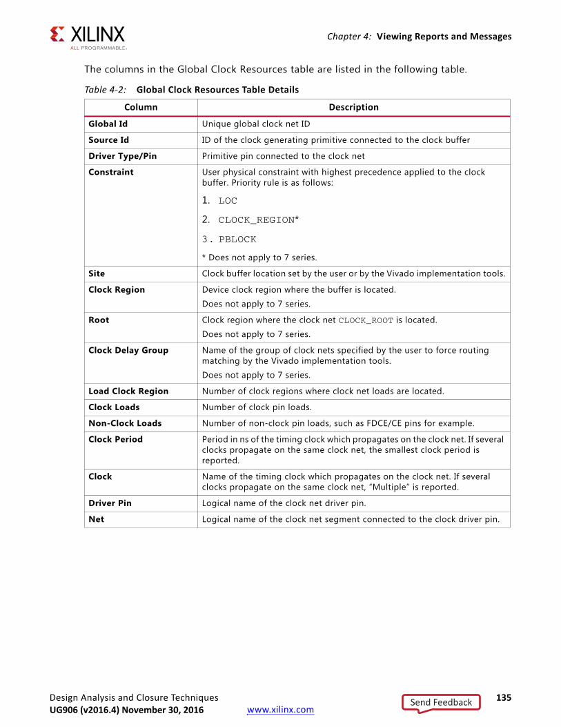
Design Analysis and Closure Techniques 135UG906 (v2016.3) October 5, 2016 www.xilinx.com
Chapter 4: Viewing Reports and Messages
The columns in the Global Clock Resources table are listed in the following table.
Table 4-2: Global Clock Resources Table Details
Column Description
Global Id Unique global clock net ID
Source Id ID of the clock generating primitive connected to the clock buffer
Driver Type/Pin Primitive pin connected to the clock net
Constraint User physical constraint with highest precedence applied to the clock buffer. Priority rule is as follows:
1. LOC
2. CLOCK_REGION*
3. PBLOCK
* Does not apply to 7 series.
Site Clock buffer location set by the user or by the Vivado implementation tools.
Clock Region Device clock region where the buffer is located.
Does not apply to 7 series.
Root Clock region where the clock net CLOCK_ROOT is located.
Does not apply to 7 series.
Clock Delay Group Name of the group of clock nets specified by the user to force routing matching by the Vivado implementation tools.
Does not apply to 7 series.
Load Clock Region Number of clock regions where clock net loads are located.
Clock Loads Number of clock pin loads.
Non-Clock Loads Number of non-clock pin loads, such as FDCE/CE pins for example.
Clock Period Period in ns of the timing clock which propagates on the clock net. If several clocks propagate on the same clock net, the smallest clock period is reported.
Clock Name of the timing clock which propagates on the clock net. If several clocks propagate on the same clock net, “Multiple” is reported.
Driver Pin Logical name of the clock net driver pin.
Net Logical name of the clock net segment connected to the clock driver pin.
Send FeedbackUG906 (v2016.4) November 30, 2016

Design Analysis and Closure Techniques 136UG906 (v2016.3) October 5, 2016 www.xilinx.com
Chapter 4: Viewing Reports and Messages
Global Clock Source Details Table
The Global Clock Source Details table shows the global clock connectivity and timing clock information for each clock generator output. The following figure shows how each output of a MMCM (src0) is connected to clock buffers. The output CLKOUT0 drives three global clocks g3, g4 and g5.
The columns in the Global Clock Resources table are listed in the following table.
X-Ref Target - Figure 4-7
Figure 4-7: Report Clock Utilization – Global Clock Source Details Table
Column Description
Source Id ID of the clock generating primitive.
Global Id Global clock ID(s) driven by the Global Clock source pin.
Driver Type/Pin Output primitive pin which generates the clock.
Constraint User physical constraint with highest precedence applied to the clock buffer. Priority rule is as follows:
1. LOC
2. PBLOCK
Site Global clock source location set by the user or by the Vivado implementation tools.
Clock Region Device clock region where the clock source is located.
Clock Loads Number of clock pin loads connected to Global Clock source pin.
Non-Clock Loads Number of non-clock pin loads, such as FDCE/CE pins for example.
Source Clock Period Period in ns of the timing clock generated by the Global Clock Source pin. If several clocks propagate on the same clock net, the smallest clock period is reported.
Clock Name of the timing clock generated by the Global Clock Source pin. If several clocks propagate on the same clock net, “Multiple” is reported.
Driver Pin Logical name of the Global Clock Source pin.
Net Logical name of the clock net segment connected to the Global Clock Source pin.
Send FeedbackUG906 (v2016.4) November 30, 2016

Design Analysis and Closure Techniques 137UG906 (v2016.3) October 5, 2016 www.xilinx.com
Chapter 4: Viewing Reports and Messages
Local Clock Details Table
The Local Clock Details table is only reported when local clocks are found in the design. A local clock is a clock net routed with regular fabric routing resources instead of global clocking resources. This situation usually occurs when a clock net is not driven by a clock buffer. The information provided by the table is similar to the one found in the Global Clock Resources table.
The following figure shows a local clock net driven by a 7 series MMCM output which directly drives a register clock pin (FDRE/C).X-Ref Target - Figure 4-8
Figure 4-8: Report Clock Utilization – Local Clock Example
Send FeedbackUG906 (v2016.4) November 30, 2016

Design Analysis and Closure Techniques 138UG906 (v2016.3) October 5, 2016 www.xilinx.com
Chapter 4: Viewing Reports and Messages
Clock Regions Tables
The Clock Regions section is only available for the UltraScale™ device families and includes several tables to cover primitive and routing resource utilization per clock region. In the Vivado IDE, you can use the Show Metrics In Device Window button to select which resource types are displayed over each clock region in the device view, as shown in the following figure.
The Clock Regions tables are:
• Clock Primitives: Utilization of each clock primitive type in each clock region.
• Load Primitives: Utilization of non-clock sequential primitives in each clock region.
X-Ref Target - Figure 4-9
Figure 4-9: Report Clock Utilization - Clock Region Resource Utilization Metrics in Device Window
Send FeedbackUG906 (v2016.4) November 30, 2016

Design Analysis and Closure Techniques 139UG906 (v2016.3) October 5, 2016 www.xilinx.com
Chapter 4: Viewing Reports and Messages
For both Clock Primitives and Load Primitives table, the Global Clock column shows the number of global clock nets routed on the horizontal distribution layer with or without loads in the reported clock region. Clock nets routed on the vertical distribution layer with no branching to the horizontal layer in the reported clock region are not counted. Clock nets routed on the routing layer are not counted.
• Global Clock Summary: Shows the utilization of Global Clocks per clock region in a table which corresponds to the device clock region floorplan, as shown in the following figure. This table is only available in the text report.
• Routing Resource Utilization: Shows the global clock routing resource utilization per type and per clock region.
Key Resource Utilization Table
The Key Resource Utilization table is only available for 7 series devices and is equivalent to the combination of all Clock Regions tables for UltraScale devices. The Global Clock Summary table is also available in the text report only.
Global Clocks Tables
The Global Clocks tables report the type of loads in each clock region for each global clock net, as well as timing clock information and the clock track ID used to route the clock net. When sorting the table by Global ID in the Vivado IDE, the clock regions where each global clock net is routed can easily be identified and highlighted in the device by simply selecting the corresponding table rows.
The column description is the same as in the Clock Primitive Utilization, Global Clock Resources, and Global Clock Source Details tables.
X-Ref Target - Figure 4-10
Figure 4-10: Report Clock Utilization – Global Clock Summary Example
Send FeedbackUG906 (v2016.4) November 30, 2016
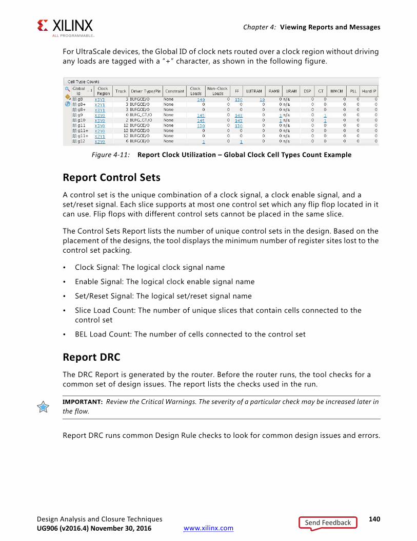
Design Analysis and Closure Techniques 140UG906 (v2016.3) October 5, 2016 www.xilinx.com
Chapter 4: Viewing Reports and Messages
For UltraScale devices, the Global ID of clock nets routed over a clock region without driving any loads are tagged with a “+” character, as shown in the following figure.
Report Control SetsA control set is the unique combination of a clock signal, a clock enable signal, and a set/reset signal. Each slice supports at most one control set which any flip flop located in it can use. Flip flops with different control sets cannot be placed in the same slice.
The Control Sets Report lists the number of unique control sets in the design. Based on the placement of the designs, the tool displays the minimum number of register sites lost to the control set packing.
• Clock Signal: The logical clock signal name
• Enable Signal: The logical clock enable signal name
• Set/Reset Signal: The logical set/reset signal name
• Slice Load Count: The number of unique slices that contain cells connected to the control set
• BEL Load Count: The number of cells connected to the control set
Report DRC The DRC Report is generated by the router. Before the router runs, the tool checks for a common set of design issues. The report lists the checks used in the run.
IMPORTANT: Review the Critical Warnings. The severity of a particular check may be increased later in the flow.
Report DRC runs common Design Rule checks to look for common design issues and errors.
X-Ref Target - Figure 4-11
Figure 4-11: Report Clock Utilization – Global Clock Cell Types Count Example
Send FeedbackUG906 (v2016.4) November 30, 2016

Design Analysis and Closure Techniques 141UG906 (v2016.3) October 5, 2016 www.xilinx.com
Chapter 4: Viewing Reports and Messages
Elaborated Design
The tool checks for DRCs related to I/O, Clock Placement, potential coding issues with your HDL, and XDC constraints. The RTL netlist typically does not have all the I/O Buffers, Clock Buffers, and other primitives the post synthesis designs have. Elaborated Design DRCs do not check for as many errors as later DRCs.
Synthesized Design and Implemented Design
• Checks for DRCs related to the post synthesis netlist.
• Checks for I/O, BUFG, and other placement.
• Basic checks on the attributes wiring on MGTs, IODELAYs, and other primitives.
• The same DRCs run taking into account any available placement and routing.
• DRCs have four severities: Info, Warning, Critical Warning, and Error. Critical Warnings and Errors do not block the design flow at this point.
Steps of the implementation flow also run the DRCs, which can stop the flow at critical points. The placer and router check for issues that block placement. Certain messages have a lower severity depending on the stage. These are DRCs flagging conditions that do not stop opt_design, place_design, or route_design from completing, but which can lead to issues on the board.
For example, some DRCs check that the user has manually constrained the package pin location and the I/O standard for all design ports. If some of these constraints are missing, place_design and route_design issue critical warnings. However, these DRCs appear as an ERROR in write_bitstream. The tools will not program a part without these constraints.
The decreased severity earlier in the flow allows you to run the design through implementation iterations before the final pinout has been determined. You must run bitstream generation for a comprehensive DRC signoff.
Figure 4-12 shows the Vivado IDE graphical user interface form of Report DRC.
Send FeedbackUG906 (v2016.4) November 30, 2016

Design Analysis and Closure Techniques 142UG906 (v2016.3) October 5, 2016 www.xilinx.com
Chapter 4: Viewing Reports and Messages
Click a DRC to open the properties for a detailed version of the message. Look in the Properties window to view the details. Most messages have a hyperlink for nets, cells, and ports referenced in the DRC.
The DRC report is static. You must rerun Report DRC for the report to reflect design changes. The tool determines that the links are stale after certain design operations (such as deleting objects and moving objects), and invalidates the links.
Selecting an object from the hyperlink selects the object, but does not refresh the Properties window. To display the properties for the object, unselect and reselect it.
To create a DRC report in Tcl, run the command report_drc.
To write the results to a file, run the command report_drc -file myDRCs.txt.
TIP: For more information on report_drc, run report_drc -help.
X-Ref Target - Figure 4-12
Figure 4-12: DRC Report
X-Ref Target - Figure 4-13
Figure 4-13: DRC Properties
Send FeedbackUG906 (v2016.4) November 30, 2016

Design Analysis and Closure Techniques 143UG906 (v2016.3) October 5, 2016 www.xilinx.com
Chapter 4: Viewing Reports and Messages
Report Route StatusThe Route Status Report is generated during the implementation flow and is available by using the report_route_status Tcl command.
The Route Status Report displays a breakdown of the nets in the design as follows:
• The total number of logical nets in the design
° The number of nets that do not need routing resources
- The number of nets that do not use routing resources outside of a tile. Examples include nets inside of a CLB, BlockRam, or I/O Pad.
- The number of Nets without loads, if any exist
° The number of routable nets that require routing resources
- The number of unrouted nets, if any exist
- The number of fully routed nets
° The number of nets with routing errors
- The number of nets with some unrouted pins, if any exist
- The number of nets with antennas/islands, if any exist
- The number of nets with resource conflicts, if any exist
The following is an example of the Report Route Status for a fully routed design:
Design Route Status : # nets : ------------------------------------------- : ----------- : # of logical nets.......................... : 6137 : # of nets not needing routing.......... : 993 : # of internally routed nets........ : 993 : # of routable nets..................... : 5144 : # of fully routed nets............. : 5144 : # of nets with routing errors.......... : 0 : ------------------------------------------- : ----------- :
Send FeedbackUG906 (v2016.4) November 30, 2016

Design Analysis and Closure Techniques 144UG906 (v2016.3) October 5, 2016 www.xilinx.com
Chapter 4: Viewing Reports and Messages
Report NoiseThe Report Noise command performs the Simultaneous Switching Noise (SSN) calculation for Xilinx 7 series FPGA devices. By default, the Noise report opens in a new tab in the Noise window area of the Vivado IDE. You can export the results to a CSV or HTML file.
The Noise Report has four sections:
• Noise Report Summary Section
• Noise Report Messages Section
• Noise Report I/O Bank Details Section
• Noise Report Links Section
Noise Report Summary Section
The Summary section of the Noise Report includes:
• When the report ran
• Number and percentage of applicable ports analyzed
• Status, including whether it passed
• Number of Critical Warnings, Warnings, and Info messages
Noise Report Messages Section
The Messages section of the Noise Report includes a detailed list of the messages generated during the report.
X-Ref Target - Figure 4-14
Figure 4-14: Run SSN Analysis
Send FeedbackUG906 (v2016.4) November 30, 2016

Design Analysis and Closure Techniques 145UG906 (v2016.3) October 5, 2016 www.xilinx.com
Chapter 4: Viewing Reports and Messages
Noise Report I/O Bank Details Section
The I/O Bank Details section of the Noise Report includes a list of Pins, Standards, and Remaining Margin.
Noise Report Links Section
The Links section of the Noise Report contains links to documentation located online at www.xilinx.com/support.
To create an HTML version of the report, select the option or run the following Tcl command:
report_ssn -format html -file myImplementedDesignSSN.html
Report Power The Power Report is generated after routing to report details of power consumption based on the current operating conditions of the device and the switching rates of the design. Power analysis requires a synthesized netlist or a placed and routed design.
• Use the set_operating_conditions command to set operating conditions.
• Use the set_switching_activity command to define switching activity.
The Report Power command is available when a Synthesized Design or an Implemented Design is open.
X-Ref Target - Figure 4-15
Figure 4-15: Noise Report
Send FeedbackUG906 (v2016.4) November 30, 2016
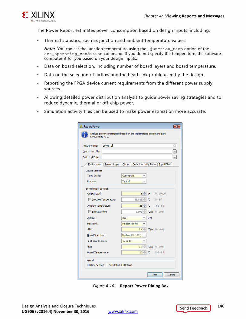
Design Analysis and Closure Techniques 146UG906 (v2016.3) October 5, 2016 www.xilinx.com
Chapter 4: Viewing Reports and Messages
The Power Report estimates power consumption based on design inputs, including:
• Thermal statistics, such as junction and ambient temperature values.
Note: You can set the junction temperature using the -junction_temp option of the set_operating_condition command. If you do not specify the temperature, the software computes it for you based on your design inputs.
• Data on board selection, including number of board layers and board temperature.
• Data on the selection of airflow and the head sink profile used by the design.
• Reporting the FPGA device current requirements from the different power supply sources.
• Allowing detailed power distribution analysis to guide power saving strategies and to reduce dynamic, thermal or off-chip power.
• Simulation activity files can be used to make power estimation more accurate.X-Ref Target - Figure 4-16
Figure 4-16: Report Power Dialog Box
Send FeedbackUG906 (v2016.4) November 30, 2016

Design Analysis and Closure Techniques 147UG906 (v2016.3) October 5, 2016 www.xilinx.com
Chapter 4: Viewing Reports and Messages
Analyzing the Power Report
Use the Report Power dialog box (Figure 4-16) to analyze power based on:
• Settings
• Power total
• Hierarchy
• Voltage rail
• Block type
For more information on the power report and analyzing the results, see the Vivado Design Suite User Guide: Power Analysis and Optimization (UG907) [Ref 8].
A text version of the power report is generated by default after route during the implementation process.
Reporting Power in a Non-Project Flow
In the non-project flow, report_power is available after link_design or synth_design. The report generated uses the available placement and routing to give more accurate power numbers. To generate this report from the Tcl Console or a script, run report_power.
X-Ref Target - Figure 4-17
Figure 4-17: Power Report
Send FeedbackUG906 (v2016.4) November 30, 2016

Design Analysis and Closure Techniques 148UG906 (v2016.3) October 5, 2016 www.xilinx.com
Chapter 5
Performing Timing Analysis
Introduction to Timing AnalysisThe Xilinx® Vivado® Integrated Design Environment (IDE) provides several reporting commands to verify that your design meets all timing constraints and is ready to be loaded on the application board. Report Timing Summary is the timing signoff report, equivalent to TRCE in the ISE® Design Suite. Report Timing Summary provides a comprehensive overview of all the timing checks, and shows enough information to allow you to start analyzing and debugging any timing issue. For more information, see Chapter 1, Logic Analysis Within the IDE.
You can generate this report in a window, write it to a file, or print it in your log file. Whenever Report Timing Summary shows that your design does not meet timing, or is missing some constraints, you can explore the details provided in the various sections of the summary and run more specific analysis. The other timing reports provide more details on a particular situation or to scope the analysis to some logic by using filters.
Before adding timing constraints to your design, you must understand the fundamentals of timing analysis, and the terminology associated with it. This chapter discusses some of key concepts used by the Xilinx Vivado Integrated Design Environment (IDE) timing engine.
Terminology• The launch edge is the active edge of the source clock that launches the data.
• The capture edge is the active edge on the destination clock that captures the data.
• The source clock is also referred to as the launch clock.
• The destination clock is also referred to as the capture clock.
• The setup requirement is the relationship between the launch edge and the capture edge that defines the most restrictive setup constraint.
• The setup relationship is the setup check verified by the timing analysis tool.
• The hold requirement is the relationship between the launch edge and capture edge that defines the most restrictive hold constraint.
• The hold relationship is the hold check verified by the timing analysis tool.
Send FeedbackUG906 (v2016.4) November 30, 2016

Design Analysis and Closure Techniques 149UG906 (v2016.3) October 5, 2016 www.xilinx.com
Chapter 5: Performing Timing Analysis
Timing PathsTiming paths are defined by the connectivity between the instances of the design. In digital designs, timing paths are formed by a pair of sequential elements controlled by the same clock, or by two different clocks.
Common Timing Paths
The most common paths in any design are:
• Path from Input Port to Internal Sequential Cell
• Internal Path from Sequential Cell to Sequential Cell
• Path from Internal Sequential Cell to Output Port
• Path from Input Port to Output Port
Path from Input Port to Internal Sequential Cell
In a path from an input port to a sequential cell, the data:
• Is launched outside the device by a clock on the board.
• Reaches the device port after a delay called the input delay [Synopsys Design Constraints (SDC) definition].
• Propagates through the device internal logic before reaching a sequential cell clocked by the destination clock.
Internal Path from Sequential Cell to Sequential Cell
In an internal path from sequential cell to sequential cell, the data:
• Is launched inside the device by a sequential cell, which is clocked by the source clock.
• Propagates through some internal logic before reaching a sequential cell clocked by the destination clock.
Path from Internal Sequential Cell to Output Port
In a path from an internal sequential cell to an output port, the data:
• Is launched inside the device by a sequential cell, which is clocked by the source clock.
• Propagates through some internal logic before reaching the output port.
• Is captured by a clock on the board after an additional delay called the output delay (SDC definition).
Send FeedbackUG906 (v2016.4) November 30, 2016

Design Analysis and Closure Techniques 150UG906 (v2016.3) October 5, 2016 www.xilinx.com
Chapter 5: Performing Timing Analysis
Path from Input Port to Output Port
In a path from an input port to output port, the data traverses the device without being latched. This type of path is also commonly called an in-to-out path. The input and output delays reference clock can be a virtual clock or a design clock.
Timing Paths Example
Figure 5-1 shows the paths described above. In this example, the design clock CLK0 can be used as the board clock for both DIN and DOUT delay constraints.
Timing Path Sections
Each timing path is composed of three sections:
• Source Clock Path
• Data Path
• Destination Clock Path
Source Clock Path
The source clock path is the path followed by the source clock from its source point (typically an input port) to the clock pin of the launching sequential cell. For a timing path starting from an input port, there is no source clock path.
X-Ref Target - Figure 5-1
Figure 5-1: Timing Paths Example
REGB
D Q
REGA
D Q
Tsetup Thold
CLK0
Board Device
D Q D QDIN DOUT
Board Clock
FPGA DEVICE
BUFG
Input Delay
Output Delay
Data Path DelayInternal Delay Internal Delay
Tclk-Q Tsetup Thold
Board Clock
Tclk-Q
In-2-Out Data Path
Board Device
Send FeedbackUG906 (v2016.4) November 30, 2016

Design Analysis and Closure Techniques 151UG906 (v2016.3) October 5, 2016 www.xilinx.com
Chapter 5: Performing Timing Analysis
Data Path
The data path is the section of the timing path where the data propagates, between the path startpoint and the path endpoint. The following definitions apply: (1) A path startpoint is a sequential cell clock pin or a data input port; and (2) A path endpoint is a sequential cell data input pin or a data output port.
Destination Clock Path
The destination clock path is the path followed by the destination clock from its source point, typically an input port, to the clock pin of the capturing sequential cell. For a timing path ending at an output port, there is no destination clock path. Figure 5-2 shows the three sections of a typical timing path.
Launch and Capture Edges
When transferring between sequential cells or ports, the data is:
• Launched by one of the edges of the source clock, which is called the launch edge.
• Captured by one of the edges of the destination clock, which is called the capture edge.
In a typical timing path, the data is transferred between two sequential cells within one clock period. In that case: (1) the launch edge occurs at 0ns; and (2) the capture edge occurs one period after.
The following section explains how the launch and capture edges define the setup and hold relationships used for timing analysis.
X-Ref Target - Figure 5-2
Figure 5-2: Typical Timing Path
REGB
D Q
REGA
D QData Path
Destination Clock Path
Source Clock Path Startpoint
Endpoint
Send FeedbackUG906 (v2016.4) November 30, 2016

Design Analysis and Closure Techniques 152UG906 (v2016.3) October 5, 2016 www.xilinx.com
Chapter 5: Performing Timing Analysis
Understanding the Basics of Timing AnalysisMax and Min Delay Analysis
Timing analysis is the static verification that a design timing behavior will be predictable once loaded and run on hardware. It considers a range of manufacturing and environmental variations that are combined into delay models that are grouped by timing corners and corner variations. It is sufficient to analyze timing against all the recommended corners, and for each corner, to perform all the checks under the most pessimistic conditions. For example, a design targeted to a Xilinx FPGA device must pass the four following analyses:
• Max delay analysis in Slow Corner
• Min delay analysis in Slow Corner
• Max delay analysis in Fast Corner
• Min delay analysis in Fast Corner
Depending on the check performed, the delays that represent the most pessimistic situation are used. This is the reason why the following checks and delay types are always associated:
• Max delay with setup and recovery checks
• Min delay with hold and removal checks
Max delay with setup and recovery checks
• The slowest delays of a given corner are used for the source clock path and data/reset path accumulated delay.
• The fastest delays of the same corner are used for the destination clock path accumulated delay.
Min delay with hold and removal checks
• The fastest delays of a given corner are used for the source clock path and data/reset path accumulated delay.
• The slowest delays of the same corner are used for the destination clock path accumulated delay.
When mapped to the various corners, these checks become:
• setup/recovery (max delay analysis)
• hold/removal (min delay analysis)
Send FeedbackUG906 (v2016.4) November 30, 2016

Design Analysis and Closure Techniques 153UG906 (v2016.3) October 5, 2016 www.xilinx.com
Chapter 5: Performing Timing Analysis
setup/recovery (max delay analysis)
• source clock(Slow_max), datapath(Slow_max), destination clock (Slow_min)
• source clock(Fast_max), datapath(Fast_max), destination clock (Fast_min)
hold/removal (min delay analysis)
• source clock(Slow_min), datapath(Slow_min), destination clock (Slow_max)
• source clock(Fast_min), datapath(Fast_min), destination clock (Fast_max)
Delays from different corners are never mixed on a same path for slack computation.
Most often, setup or recovery violations occur with Slow corner delays, and hold or removal violations occur with Fast corner delays. However, since this is not always true (especially for I/O timing) Xilinx recommends that you perform both analyses on both corners.
Setup/Recovery Relationship
The setup check is performed only on the most pessimistic setup relationship between two clocks. By default, this corresponds to the smallest positive delta between the launch and capture edges. For example, consider a path between two flip-flops that are sensitive to the rising edge of their respective clock. The launch and capture edges of this path are the clock rising edges only.
The clocks are defined as follows:
• clk0 has a period of 6 ns with first rising @ 0 ns and falling edge @ 3 ns.
• clk1 has a period of 4 ns with first rising @ 0 ns and falling edge @ 2 ns.
As Figure 5-3 shows, there are two unique setup relationships: Setup(1) and Setup(2).
X-Ref Target - Figure 5-3
Figure 5-3: Setup Relationships
Common period
0ns 2ns 4ns 6ns 8ns 10ns 12ns
clk0 launch edges(source clock)
clk1 capture edges(destination clock)
Setup(1) Setup(2)
X13434
Send FeedbackUG906 (v2016.4) November 30, 2016

Design Analysis and Closure Techniques 154UG906 (v2016.3) October 5, 2016 www.xilinx.com
Chapter 5: Performing Timing Analysis
The smallest positive delta from clk0 to clk1 is 2 ns, which corresponds to Setup(2). The Common Period is 12ns, which corresponds to the time between two simultaneous alignments of the two clocks.
TIP: The relationships are established when considering the ideal clock waveforms, that is, before applying the insertion delay from the clock root to the flip-flop clock pin.
IMPORTANT: If the common period cannot be found over 1000 cycles of both clocks, the worst setup relationship over these 1000 cycles is used for timing analysis. For such case, the two clocks are called unexpandable, or clocks with no common period. The analysis will likely not correspond to the most pessimistic scenario. You must review the paths between these clocks to assess their validity and determine if they can be treated as asynchronous paths instead.
Once the path requirement is known, the path delays, the clocks uncertainty and the setup time are introduced to compute the slack. The typical slack equation is:
As the equation shows, a positive setup slack occurs when the data arrives before the required time.
The recovery check is similar to the setup check, except that it applies to asynchronous pins such as preset or clear. The relationships are established the same way as for setup, and the slack equation is the same except that the recovery time is used instead of the setup time.
Hold/Removal Relationship
The hold check (also called hold relationship) is directly connected to the setup relationship. While the setup analysis ensures that data can safely be captured under the most pessimistic scenario, the hold relationship ensures that:
• The data sent by the setup launch edge cannot be captured by the active edge before the setup capture edge (H1a and H2a corresponding to setup edges S1 and S2 respectively in Figure 5-4).
• The data sent by the next active source clock edge after the setup launch edge cannot be captured by the setup capture edge (H2a and H2b corresponding to setup edges S1 and S2 respectively in Figure 5-4).
Data Required Time (setup) = capture edge time
+ destination clock path delay
- clock uncertainty
- setup time
Data Arrival Time (setup) = launch edge time
+ source clock path delay
+ datapath delay
Slack (setup) = Data Required Time - Data Arrival Time
Send FeedbackUG906 (v2016.4) November 30, 2016

Design Analysis and Closure Techniques 155UG906 (v2016.3) October 5, 2016 www.xilinx.com
Chapter 5: Performing Timing Analysis
During hold analysis, the timing engine reports only the most pessimistic hold relationship between any two clocks. The most pessimistic hold relationship is not always associated with the worst setup relationship. The timing engine must review all possible setup relationships and their corresponding hold relationships to identify the most pessimistic hold relationship.
For example, consider the same path as in the setup relationship example. Two unique setup relationships exist.
The following figure illustrates the two hold relationships per setup relationship.
The greatest hold requirement is 0ns, which corresponds to the first rising edge of both source and destination clocks.
Once the path requirement is known, the path delays, the clocks’ uncertainty, and the hold time are introduced to compute the slack. The typical slack equation is:
As the equation shows, the hold slack is positive when the new data arrives after the required time.
The removal check is similar to the hold check, except that it applies to asynchronous pins such as preset or clear. The relationships are established the same way as for hold, and the slack equation is the same except that the removal time is used instead of the hold time.
X-Ref Target - Figure 5-4
Figure 5-4: Hold Relationships per Setup Relationship
Data Required Time (hold) = capture edge time
+ destination clock path delay
- clock uncertainty
+ hold time
Data Arrival Time (hold) = launch edge time
+ source clock path delay
+ datapath delay
Slack (hold) = Data Arrival Time - Data Required Time
0ns 2ns 4ns 6ns 8ns 10ns 12ns
clk0 launch edges(source clock)
clk1 capture edges(destination clock)
H1a S1 H1b H2a S2 H2b
X13435
Send FeedbackUG906 (v2016.4) November 30, 2016
Design Analysis and Closure Techniques 156UG906 (v2016.3) October 5, 2016 www.xilinx.com
Chapter 5: Performing Timing Analysis
Path Requirement
The path requirement represents the difference in time between the capture edge and the launch edge of a timing path.
For example, when considering the same path and clocks as in the previous section, the following path requirements exist:
Setup Path Requirement (S1) = 1*T(clk1) - 0*T(clk0) = 4nsSetup Path Requirement (S2) = 2*T(clk1) - 1*T(clk0) = 2ns
The corresponding hold relationships are:
• Corresponding to setup S1
Hold Path Requirement (H1a) = (1-1)*T(clk1) - 0*T(clk0) = 0nsHold Path Requirement (H1b) = 1*T(clk1) - (0+1)*T(clk0) = -2ns
• Corresponding to setup S2
Hold Path Requirement (H2a) = (2-1)*T(clk1) - 1*T(clk0) = -2nsHold Path Requirement (H2b) = 2*T(clk1) - (1+1)*T(clk0) = -4ns
The timing analysis is performed only with the two most pessimistic requirements. In the example above, these are:
• The setup requirement S2
• The hold requirement H1a
Clock Phase Shift
A clock phase-shift corresponds to a delayed clock waveform with respect to a reference clock due to special hardware in the clock path. In Xilinx FPGAs, clock phase-shift is usually introduced by the MMCM or PLL primitives, when their output clock property CLKOUT*_PHASE is non-zero.
Send FeedbackUG906 (v2016.4) November 30, 2016
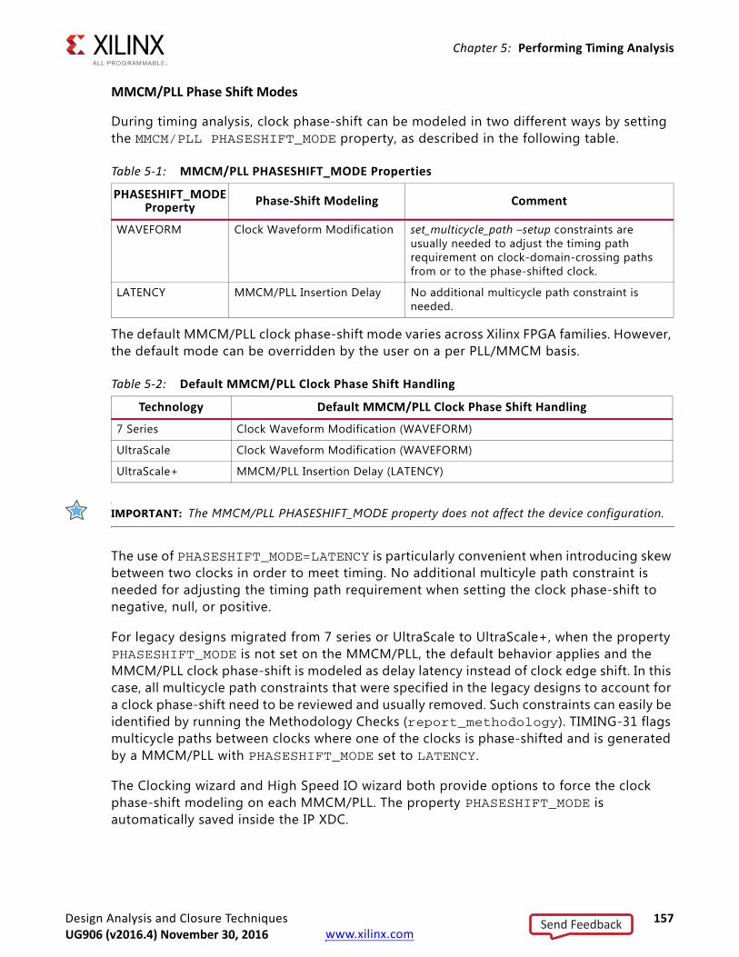
Design Analysis and Closure Techniques 157UG906 (v2016.3) October 5, 2016 www.xilinx.com
Chapter 5: Performing Timing Analysis
MMCM/PLL Phase Shift Modes
During timing analysis, clock phase-shift can be modeled in two different ways by setting the MMCM/PLL PHASESHIFT_MODE property, as described in the following table.
:
The default MMCM/PLL clock phase-shift mode varies across Xilinx FPGA families. However, the default mode can be overridden by the user on a per PLL/MMCM basis.
IMPORTANT: The MMCM/PLL PHASESHIFT_MODE property does not affect the device configuration.
The use of PHASESHIFT_MODE=LATENCY is particularly convenient when introducing skew between two clocks in order to meet timing. No additional multicyle path constraint is needed for adjusting the timing path requirement when setting the clock phase-shift to negative, null, or positive.
For legacy designs migrated from 7 series or UltraScale to UltraScale+, when the property PHASESHIFT_MODE is not set on the MMCM/PLL, the default behavior applies and the MMCM/PLL clock phase-shift is modeled as delay latency instead of clock edge shift. In this case, all multicycle path constraints that were specified in the legacy designs to account for a clock phase-shift need to be reviewed and usually removed. Such constraints can easily be identified by running the Methodology Checks (report_methodology). TIMING-31 flags multicycle paths between clocks where one of the clocks is phase-shifted and is generated by a MMCM/PLL with PHASESHIFT_MODE set to LATENCY.
The Clocking wizard and High Speed IO wizard both provide options to force the clock phase-shift modeling on each MMCM/PLL. The property PHASESHIFT_MODE is automatically saved inside the IP XDC.
Table 5-1: MMCM/PLL PHASESHIFT_MODE Properties
PHASESHIFT_MODE Property Phase-Shift Modeling Comment
WAVEFORM Clock Waveform Modification set_multicycle_path –setup constraints are usually needed to adjust the timing path requirement on clock-domain-crossing paths from or to the phase-shifted clock.
LATENCY MMCM/PLL Insertion Delay No additional multicycle path constraint is needed.
Table 5-2: Default MMCM/PLL Clock Phase Shift Handling
Technology Default MMCM/PLL Clock Phase Shift Handling
7 Series Clock Waveform Modification (WAVEFORM)
UltraScale Clock Waveform Modification (WAVEFORM)
UltraScale+ MMCM/PLL Insertion Delay (LATENCY)
Send FeedbackUG906 (v2016.4) November 30, 2016

Design Analysis and Closure Techniques 158UG906 (v2016.3) October 5, 2016 www.xilinx.com
Chapter 5: Performing Timing Analysis
Phase Shift in Timing Reports
A positive phase shift moves the source clock edge forward, delaying the clock edge. A negative phase shift moves the source clock edge backward. The modification of the clock waveform result in potentially different clock edges being used by the STA for the source and capture clocks.
In the examples below, clock clkout0 (period 10 ns) is auto-derived by a MMCM.
• No phase shift
vivado% set_property CLKOUT0_PHASE 0.000 [get_cells qpll/plle2_adv_inst]vivado% report_timing...(clock clkout0 rise edge) 0.000 0.000 r... MMCME2_ADV (Prop_mmcme2_adv_CLKIN1_CLKOUT0) -5.411 5.903 r mmcm_inst/mmcm_adv_inst/CLKOUT0...
The source clock edge is 0.0 ns.
• Positive phase shift of 12.0 with PHASESHIFT_MODE=WAVEFORM
vivado% set_property CLKOUT0_PHASE 12.000 [get_cells qpll/plle2_adv_inst]vivado% report_timing...(clock clkout0 rise edge) 0.333 0.333 r... MMCME2_ADV (Prop_mmcme2_adv_CLKIN1_CLKOUT0) -5.411 5.903 r mmcm_inst/mmcm_adv_inst/CLKOUT0...
The source clock edge is delayed by 0.333 ns (10 ns / 360 * 12.0).
• Positive phase shift of 12.0 with PHASESHIFT_MODE=LATENCY
vivado% set_property CLKOUT0_PHASE 12.000 [get_cells qpll/plle2_adv_inst]vivado% report_timing...(clock clkout0 rise edge) 0.000 0.000 r... MMCME2_ADV (Prop_mmcme2_adv_CLKIN1_CLKOUT0) -5.078 6.236 r mmcm_inst/mmcm_adv_inst/CLKOUT0 ...
The MMCM insertion delay is increased by 0.333 ns (10 ns / 360 * 12.0). The source clock edge is 0.0 ns.
Send FeedbackUG906 (v2016.4) November 30, 2016

Design Analysis and Closure Techniques 159UG906 (v2016.3) October 5, 2016 www.xilinx.com
Chapter 5: Performing Timing Analysis
• Negative phase shift of -15.0 with PHASESHIFT_MODE=WAVEFORM
vivado% set_property CLKOUT0_PHASE -15.000 [get_cells qpll/plle2_adv_inst]vivado% report_timing...(clock clkout0 rise edge) -0.417 -0.417 r... MMCME2_ADV (Prop_mmcme2_adv_CLKIN1_CLKOUT0) -5.411 5.903 r mmcm_inst/mmcm_adv_inst/CLKOUT0...
The source clock edge is moved backward by -0.417 ns (10 ns / 360 * -15.0).
• Negative phase shift of -15.0 with PHASESHIFT_MODE=LATENCY
vivado% set_property CLKOUT0_PHASE -15.000 [get_cells qpll/plle2_adv_inst]vivado% report_timing...(clock clkout0 rise edge) 0.000 0.000 r... MMCME2_ADV (Prop_mmcme2_adv_CLKIN1_CLKOUT0) -5.828 5.486 r mmcm_inst/mmcm_adv_inst/CLKOUT0 ...
The MMCM insertion delay is decreased by 0.417 ns (10 ns / 360 * -15.0). The source clock edge is 0.0 ns.
Clock Skew and Uncertainty
Skew and uncertainty both impact setup and hold computations and slack.
Skew Definition
Clock skew is the insertion delay difference between the destination clock path and the source clock path: (1) from their common point in the design; (2) to, respectively, the endpoint and startpoint sequential cell clock pins.
In the equation below:
• Tcj is the delay from the common node to the endpoint clock pin.
• Tci is the delay from the common node to the startpoint clock pin:
Tskewi,j = Tci- Tcj
Clock Pessimism Removal
A typical timing path report shows the delay details of both source and destination clock paths, from their root to the sequential cell clock pins. As explained below, the source and destination clocks are analyzed with a different delay, even on their common circuitry.
Send FeedbackUG906 (v2016.4) November 30, 2016

Design Analysis and Closure Techniques 160UG906 (v2016.3) October 5, 2016 www.xilinx.com
Chapter 5: Performing Timing Analysis
This delay difference on the common section introduces some additional pessimism in the skew computation. To avoid unrealistic slack computation, this pessimism is compensated by a delay called the Clock Pessimism Removal (CPR) value.
Clock Pessimism Removal (CPR) = common clock circuitry (max delay - min delay)
The CPR is added or subtracted to the skew depending on the type of analysis performed:
• Max Delay Analysis (Setup/Recovery)
CPR is added to the destination clock path delay.
• Min Delay Analysis (Hold/Removal)
CPR is subtracted from the destination clock path delay.
The Vivado Design Suite timing reports clock skew for each timing path as shown below (hold analysis in this case):
• DCD - Destination Clock Delay
• SCD - Source Clock Delay
• CPR - Clock Pessimism Removal
Clock Path Skew: 0.301ns (DCD - SCD - CPR)Destination Clock Delay (DCD): 2.581nsSource Clock Delay (SCD): 2.133nsClock Pessimism Removal (CPR): 0.147ns
In many cases, the CPR accuracy changes before and after routing. For example, let’s consider a timing path where the source and destination clocks are the same clock, and the startpoint and endpoint clock pins are driven by the same clock buffer.
X-Ref Target - Figure 5-5
Figure 5-5: Common Clock Tree Section
D Q
REGA
D Q
REGB
TCKQ TSETUP
Data Path Delay
Source Clock
ClockSourcePoint
Destination Clock
Common Clock Tree Section
Min DelayMax Delay
X13436
Send FeedbackUG906 (v2016.4) November 30, 2016

Design Analysis and Closure Techniques 161UG906 (v2016.3) October 5, 2016 www.xilinx.com
Chapter 5: Performing Timing Analysis
Before routing, the common point is the clock net driver, that is, the clock buffer output pin. CPR compensates only for the pessimism from the clock root to the clock buffer output pin.
After routing, the common point is the last routing resource shared by the source and destination clock paths in the device architecture. This common point is not represented in the netlist, so the corresponding CPR cannot be directly retrieved by subtracting common clock circuitry delay difference from the timing report. The timing engine computes the CPR value based on device information not directly exposed to the user.
Optimistic Skew
Xilinx FPGA devices provide advanced clocking resources such as dedicated clock routing trees and Clock Modifying Blocks (CMB). Some of the CMBs have the capability to compensate the clock tree insertion delay by using a Phase Lock Loop circuit (present in PLL or MMCM primitives). The amount of compensation is based on the insertion delay present on the feedback loop of the PLL. In many cases, a PLL (or MMCM) drives several clock trees with the same type of buffer, including on the feedback loop. As the device can be large, the insertion delay on all these clock tree branches does not always match the feedback loop delay. The clocks driven by a PLL become over-compensated when the feedback loop delay is bigger than the source or destination clock delay. In this case, the sign of the CPR changes and it effectively removes skew optimism from the slack value. This is needed in order to ensure that there is no artificial skew at the common node of any timing path clocks during the analysis.
RECOMMENDED: Always use the CPR compensation during timing analysis to preserve the slack accuracy and the overall timing signoff quality.
Clock Uncertainty
Clock uncertainty is the total amount of possible time variation between any pair of clock edges. The uncertainty consists of the computed clock jitter (system, input, and discrete); the phase error introduced by certain hardware primitives; and any clock uncertainty specified by the user in the design constraints (set_clock_uncertainty).
For primary clocks, the jitter is defined by set_input_jitter and set_system_jitter. For clock generators such as MMCM and PLL, the tool computes the jitter based on user-specified jitter on its source clock and its configuration. For other generated clocks (such as flop based clock dividers), the jitter is the same as that of its source clock.
The user-specified clock uncertainty is added to the uncertainty computed by the Vivado Design Suite timing engine. For generated clocks (such as from MMCM, PLL, and flop-based clock dividers), uncertainty specified by the user on source clock does not propagate through the clock generators.
For more information on jitter and phase error definitions, see the Vivado Design Suite User Guide: Using Constraints (UG903) [Ref 6].
Send FeedbackUG906 (v2016.4) November 30, 2016

Design Analysis and Closure Techniques 162UG906 (v2016.3) October 5, 2016 www.xilinx.com
Chapter 5: Performing Timing Analysis
The clock uncertainty has two purposes:
• Reserve some amount of margin in the slack numbers for representing any noise on the clock that could affect the hardware functionality. Because the delay and jitter numbers are conservative, Xilinx does not recommend adding extra uncertainty to ensure proper hardware functionality.
• Over-constrain the paths related to a clock or a clock pair during one or several implementation steps. This increases the QoR margin that can be used to help the next steps to close timing on these paths. By using clock uncertainty, the clock waveforms and their relationships are not modified, so the rest of the timing constraints can still apply properly.
Pulse Width Checks
The pulse width checks are some rule checks on the signal waveforms when they reach the hardware primitives after propagation through the device. They usually correspond to functional limits dictated by the circuitry inside the primitive. For example, the minimum period check on a DSP clock pin ensures that the clock driving a DSP instance does not run at higher frequency than what is tolerated by the internal DSP.
The pulse width checks do not affect synthesis or implementation. Their analysis must be performed once before the bitstream generation like any other design rule check provided by the Vivado Design Suite.
When a pulse width violation occurs, it is due to an inappropriate clock definition (pulse width and period checks) or an inappropriate clock topology that induces too much skew (max_skew check). You must review the Xilinx FPGA data sheet of the target device to understand the operation range of the primitive where the violation occurs. In the case of a skew violation, you must simplify the clock tree or place the clock resources closer to the violating pins.
Reading a Timing Path ReportThe timing path report provides the information needed to understand what causes a timing violation. The following sections describe the Timing Path Report.
The Timing Path Summary displays the important information from the timing path details. You can review it to find out about the cause of a violation without having to analyze the details of the timing path. It includes slack, path requirement, datapath delay, cell delay, route delay, clock skew, and clock uncertainty. It does not provide any information about cell placement.
For more information about the terminology used for timing constraints and timing analysis, as well as learn how slack and path requirement are determined, see Understanding the Basics of Timing Analysis, page 152.
Send FeedbackUG906 (v2016.4) November 30, 2016

Design Analysis and Closure Techniques 163UG906 (v2016.3) October 5, 2016 www.xilinx.com
Chapter 5: Performing Timing Analysis
Timing Path Summary Header ExamplesFigure 5-6 shows an example of the Timing Path Summary Header in a text report.
Figure 5-7 shows an example of the Timing Path Summary header in the Vivado IDE.
Timing Path Summary Header InformationThe Timing Path Summary header includes the following information:
• Slack
A positive slack indicates that the path meets the path requirement, which is derived from the timing constraints. The Slack equation depends on the analysis performed.
° Max delay analysis (setup/recovery)slack = data required time - data arrival time
° Min delay analysis (hold/removal)slack = data arrival time - data required time
Data required and arrival times are calculated and reported in the other subsections of the timing path report.
X-Ref Target - Figure 5-6
Figure 5-6: Timing Path Summary Header in Text Report
X-Ref Target - Figure 5-7
Figure 5-7: Timing Path Summary Header in Vivado IDE
Send FeedbackUG906 (v2016.4) November 30, 2016

Design Analysis and Closure Techniques 164UG906 (v2016.3) October 5, 2016 www.xilinx.com
Chapter 5: Performing Timing Analysis
• Source
The path startpoint and the source clock that launches the data. The startpoint is usually the clock pin of a sequential cell or an input port.
When applicable, the second line displays the primitive and the edge sensitivity of the clock pin. It also provides the clock name and the clock edges definition (waveform and period).
• Destination
The path endpoint and the destination clock that captures the data. The endpoint is usually the input data pin of the destination sequential cell or an output port. Whenever applicable, the second line displays the primitive and the edge sensitivity of the clock pin. It also provides the clock name and the clock edges definition (waveform and period).
• Path Group
The timing group that the path endpoint belongs to. This is usually the group defined by the destination clock, except for asynchronous timing checks (recovery/removal) which are grouped in the **async_default** timing group. User-defined groups can also appear here. They are convenient for reporting purpose.
• Path Type
The type of analysis performed on this path.
° Max: indicates that the maximum delay values are used to calculate the data path delay, which corresponds to setup and recovery analysis.
° Min: indicates that the minimum delay values are used to calculate the data path delay, which corresponds to hold and removal analysis.
This line also shows which corner was used for the report: Slow or Fast.
• Requirement
The timing path requirement, which is typically:
° One clock period for setup/recovery analysis.
° 0ns for hold/removal analysis, when the startpoint and endpoint are controlled by the same clock, or by clocks with no phase-shift.
When the path is between two different clocks, the requirement corresponds to the smallest positive difference between any source and destination clock edges. This value is overridden by timing exception constraints such as multicycle path, max delay and min delay.
For more information on how the timing path requirement is derived from the timing constraints, Timing Paths, page 149.
Send FeedbackUG906 (v2016.4) November 30, 2016
Design Analysis and Closure Techniques 165UG906 (v2016.3) October 5, 2016 www.xilinx.com
Chapter 5: Performing Timing Analysis
• Data Path Delay
Accumulated delay through the logic section of the path. The clock delay is excluded unless the clock is used as a data. The type of delay corresponds to what the Path Type line describes.
• Logic Levels
The number of each type of primitives included in the data section of the path, excluding the startpoint and the endpoint cells.
• Clock Path Skew
The insertion delay difference between the launch edge of the source clock and the capture edge of the destination clock, plus clock pessimism correction (if any).
• Destination Clock Delay (DCD)
The accumulated delay from the destination clock source point to the endpoint of the path.
° For max delay analysis (setup/recovery), the minimum cell and net delay values are used
° For min delay analysis (hold/removal), the maximum delay values are used.
• Source Clock Delay (SCD)
The accumulated delay from the clock source point to the startpoint of the path.
° For max delay analysis (setup/recovery), the maximum cell and net delay values are used.
° For min delay analysis (hold/removal), the minimum delay values are used.
• Clock Pessimism Removal (CPR)
The absolute amount of extra clock skew introduced by the fact that source and destination clocks are reported with different types of delay even on their common circuitry.
After removing this extra pessimism, the source and destination clocks do not have any skew on their common circuitry.
For a routed design, the last common clock tree node is usually located in the routing resources used by the clock nets and is not reported in the path details.
Send FeedbackUG906 (v2016.4) November 30, 2016
Design Analysis and Closure Techniques 166UG906 (v2016.3) October 5, 2016 www.xilinx.com
Chapter 5: Performing Timing Analysis
• Clock Uncertainty
The total amount of possible time variation between any pair of clock edges.
The uncertainty comprises the computed clock jitter (system and discrete), the phase error introduced by certain hardware primitives and any clock uncertainty specified by the user in the design constraints (set_clock_uncertainty).
The user clock uncertainty is additive to the uncertainty computed by the Vivado IDE timing engine.
• Total System Jitter (TSJ)
The combined system jitter applied to both source and destination clocks. To modify the system jitter globally, use the set_system_jitter constraint. The virtual clocks are ideal and therefore do not have any system jitter.
• Total Input Jitter (TIJ)
The combined input jitter of both source and destination clocks.
To define the input jitter for each primary clock individually, use the set_input_jitter constraint. The Vivado IDE timing engine computes the generated clocks input jitter based on their master clock jitter and the clocking resources traversed. By default, the virtual clocks are ideal and therefore do not have any jitter.
For more information on clock uncertainty and jitter, see this link in the Vivado Design Suite User Guide: Using Constraints (UG903) [Ref 6].
• Discrete Jitter (DJ)
The amount of jitter introduced by hardware primitives such as MMCM or PLL.
The Vivado IDE timing engine computes this value based on the configuration of these cells.
• Phase Error (PE)
The amount of phase variation between two clock signals introduced by hardware primitives such as MMCM or PLL.
The Vivado IDE timing engine automatically provides this value and adds it to the clock uncertainty
• User Uncertainty (UU)
The additional uncertainty specified by the set_clock_uncertainty constraint.
For more information on how to use this command, see this link in the Vivado Design Suite Tcl Command Reference Guide (UG835) [Ref 3].
Send FeedbackUG906 (v2016.4) November 30, 2016

Design Analysis and Closure Techniques 167UG906 (v2016.3) October 5, 2016 www.xilinx.com
Chapter 5: Performing Timing Analysis
Additional lines can appear in the Timing Path Summary depending on the timing constraints, the reported path, and the target device:
• Inter-SLR Compensation
The additional margin required for safely reporting paths that cross SLR boundaries in Xilinx 7 series SSI devices only.
• Input Delay
The input delay value specified by the set_input_delay constraint on the input port. This line does not show for paths that do not start from an input port.
• Output Delay
The output delay value specified by the set_output_delay constraint on the output port. This line does not show for paths that do not end to an output port.
• Timing Exception
The timing exception that covers the path. Only the exception with the highest precedence is displayed, as it is the only one affecting the timing path requirement.
For information on timing exceptions and their precedence rules, see Timing Paths.
Timing Path DetailsThe second half of the report provides more details on the cells, pins, ports and nets traversed by the path. It is separated into three sections:
• Source Clock Path
The circuitry traversed by the source clock from its source point to the startpoint of the datapath. This section does not exist for a path starting from an input port.
• Data Path
The circuitry traversed by the data from the startpoint to the endpoint.
• Destination Clock Path
The circuitry traversed by the destination clock from its source point to the datapath endpoint clock pin.
The Source Clock Path and Data Path sections work together. They are always reported with the same type of delay:
• max delay for setup/recovery analysis
• min delay for hold/removal analysis
Send FeedbackUG906 (v2016.4) November 30, 2016

Design Analysis and Closure Techniques 168UG906 (v2016.3) October 5, 2016 www.xilinx.com
Chapter 5: Performing Timing Analysis
They share the accumulated delay which starts at the data launch edge time, and accumulates delay through both source clock and data paths. The final accumulated delay value is called the data arrival time.
The destination clock path is always reported with the opposite delay to the source clock and data paths. Its initial accumulated delay value is the time when the data capture edge is launched on the destination clock source point. The final accumulated delay value is called the data required time.
The final lines of the report summarize how the slack is computed.
• For max delay analysis (setup/recovery)
slack = data required time - data arrival time
• For min delay analysis (hold/removal)
slack = data arrival time - data required time
Timing Path Details In Text Report
Figure 5-8 shows an example of the Source Clock, Data and Destination Clock Paths in the text report. Because the path is covered by a simple period constraint of 5 ns, the source clock launch edge starts at 0 ns and the destination clock capture edge starts at 5 ns.
X-Ref Target - Figure 5-8
Figure 5-8: Timing Path Details in Text Report
Send FeedbackUG906 (v2016.4) November 30, 2016

Design Analysis and Closure Techniques 169UG906 (v2016.3) October 5, 2016 www.xilinx.com
Chapter 5: Performing Timing Analysis
Timing Path Details in Vivado IDE
The Timing Path Details in the Vivado IDE, as shown in Figure 5-9, shows the same information as is shown in the text report, seen in Figure 5-8.
X-Ref Target - Figure 5-9
Figure 5-9: Timing Path Details in Vivado IDE
Send FeedbackUG906 (v2016.4) November 30, 2016

Design Analysis and Closure Techniques 170UG906 (v2016.3) October 5, 2016 www.xilinx.com
Chapter 5: Performing Timing Analysis
The information on the path is displayed in five columns:
• Location
Where the cell or port is placed on the device.
• Delay Type
The unisim primitive and the particular timing arc followed by the path. In case of a net, it shows the fanout (fo) and its status. A net can be:
° Unplaced: The driver and the load are not placed.
° Estimated: The driver or the load or both are placed. A partially routed net is also reported as estimated.
° Routed: The driver and the load are both placed, plus the net is fully routed.
• Incr(ns) (text report) / Delay (IDE report)
The value of the incremental delay associated to a unisim primitive timing arc or a net. It can also show of a constraint such as input/output delay or clock uncertainty.
• Path(ns) (text report) / Cumulative (IDE report)
The accumulated delay after each segment of the path. On a given line, its value is the accumulated value from the previous + the incremental delay of the current line.
• Netlist Resource(s) (text report) / Logical Resource (IDE report)
The name of the netlist object traversed.
Each incremental delay is associated to one of the following edge senses:
• r (rising)
• f (falling)
The initial sense of the edge is determined by the launch or capture edge used for the analysis. It can be inverted by any cell along the path, depending on the nature of the timing arc. For example, a rising edge at the input of an inverter becomes a falling edge on the output.
The edge sense can be helpful in identifying that an overly-tight timing path requirement comes from a clock edge inversion along the source or destination clock tree.
Send FeedbackUG906 (v2016.4) November 30, 2016

Design Analysis and Closure Techniques 171UG906 (v2016.3) October 5, 2016 www.xilinx.com
Chapter 5: Performing Timing Analysis
Verifying Timing SignoffBefore going into the details of timing analysis, it is important to understand which part of the timing reports indicates that your design is ready to run in hardware.
IMPORTANT: Timing signoff is a mandatory step in the analysis of the implementation results, once your design is fully placed and routed.
By default, when using projects in the Vivado Design Suite, the runs automatically generate the text version of Report Timing Summary. You can also generate this report interactively after loading the post-implementation design checkpoint in memory.
IMPORTANT: Report Timing Summary does not cover the bus skew constraints. To report the bus skew constraints, you must run the report_bus_skew command separately on the command line. There is no GUI support for this command.
For a comprehensive Timing Signoff Verification methodology, see this link in the UltraFast Design Methodology Guide for the Vivado Design Suite (UG949) [Ref 5].
Send FeedbackUG906 (v2016.4) November 30, 2016

Design Analysis and Closure Techniques 172UG906 (v2016.3) October 5, 2016 www.xilinx.com
Chapter 6
Synthesis Analysis and Closure Techniques
Using the Elaborated View to Optimize the RTLWhen analyzing the timing results after any implementation step with report_timing, report_timing_summary or report_design_analysis, you must review the structure of critical paths to understand if they can be mapped to logic primitives more efficiently by modifying the RTL, using synthesis attributes, or using different synthesis options. This is especially important for paths with high number of logic levels, which stress the implementation tools and limit the overall design performance.
Whenever you find a critical path with a high number of logic levels, you must question whether the functionality of the path requires so many logic levels or not. It is usually not easy to determine the optimal number of logic levels because it depends on your knowledge of the design and your knowledge of RTL optimization in general. It is a complex task to look at the post-synthesis optimized netlist and identify where the problem comes from in the RTL and how to improve it.
In project mode, the Vivado IDE helps simplifying the analysis by providing a powerful cross-probing mechanism between the synthesized or implemented design and the elaborated design. Do the following to cross-probe the synthesized/implemented design and the elaborated design:
1. Open both the synthesized/implemented design and the elaborated design in memory.
2. Select the timing path in the synthesized/implemented design view and show its schematics by pressing the F4 key.
3. Select the Elaborated Design in the Flow Navigator pane. The RTL cells that correspond to the timing path are also selected, so that you can open the RTL schematics (by pressing the F4 key) to view the same path in the elaborated view or trace from the endpoint pin back to the startpoint cell.
4. Review the RTL logic traversed by the path, especially the size of the operators or vectors.
Send FeedbackUG906 (v2016.4) November 30, 2016

Design Analysis and Closure Techniques 173UG906 (v2016.3) October 5, 2016 www.xilinx.com
Chapter 6: Synthesis Analysis and Closure Techniques
ExampleIn the following example, a user has written a counter as follows:
The signal cnt counts from 0 to 16, which requires a 5-bit vector to encode. The post-route critical schematics is shown in Figure 6-2. The endpoint is the bit 30 of the cnt signal.
After selecting the startpoint and endpoint cells of the critical path, you can visualize the equivalent path in the elaborated view by opening a schematics of the selected cells and expanding the logic from the endpoint pin back to the startpoint, as shown in Figure 6-3.
X-Ref Target - Figure 6-1
Figure 6-1: Simple Counter VHDL Example
X-Ref Target - Figure 6-2
Figure 6-2: cnt Counter Post-Route Critical Path Schematic
X-Ref Target - Figure 6-3
Figure 6-3: cnt Counter in the Elaborated View
Send FeedbackUG906 (v2016.4) November 30, 2016

Design Analysis and Closure Techniques 174UG906 (v2016.3) October 5, 2016 www.xilinx.com
Chapter 6: Synthesis Analysis and Closure Techniques
The elaborated view shows that the adder-input has been sized to 32 bit, because the signal cnt is declared as an integer. In this particular example, the 32-bit operator is retained throughout the synthesis optimizations. The elaborated view gives a good hint of what is happening and you can change the RTL as follows in order to get a better optimized netlist and timing QoR. As the counter increments from 0 to 16, you can define a range for the signal cnt which forces the adder-inputs to be 5 bits wide instead of 32 bits wide.
The change made to the RTL code will subsequently impact the synthesis optimization, which you can verify using the elaborated view instead of going through the entire compilation flow:
X-Ref Target - Figure 6-4
Figure 6-4: Simple Counter VHDL example with Integer Range
X-Ref Target - Figure 6-5
Figure 6-5: cnt Counter in the Elaborated View after RTL improvement
Send FeedbackUG906 (v2016.4) November 30, 2016

Design Analysis and Closure Techniques 175UG906 (v2016.3) October 5, 2016 www.xilinx.com
Chapter 6: Synthesis Analysis and Closure Techniques
Optimizing RAMB Utilization when Memory Depth is not a Power of 2The following test case can be used to observe the log file generated by the synthesis tool and see if there is any improvement that can be done to the RTL to guide the tool in a better way. The following code snippet shows a 40K-deep 36-bit wide memory description in VHDL. The address bus requires 16 bits.X-Ref Target - Figure 6-6
Figure 6-6: 40K x 36 bits Memory RTL Example
Send FeedbackUG906 (v2016.4) November 30, 2016
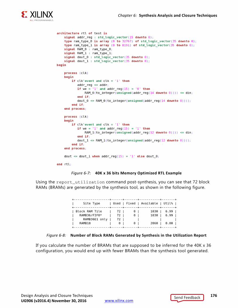
Design Analysis and Closure Techniques 176UG906 (v2016.3) October 5, 2016 www.xilinx.com
Chapter 6: Synthesis Analysis and Closure Techniques
Using the report_utilization command post-synthesis, you can see that 72 block RAMs (BRAMs) are generated by the synthesis tool, as shown in the following figure.
If you calculate the number of BRAMs that are supposed to be inferred for the 40K x 36 configuration, you would end up with fewer BRAMs than the synthesis tool generated.
X-Ref Target - Figure 6-7
Figure 6-7: 40K x 36 bits Memory Optimized RTL Example
X-Ref Target - Figure 6-8
Figure 6-8: Number of Block RAMs Generated by Synthesis in the Utilization Report
Send FeedbackUG906 (v2016.4) November 30, 2016

Design Analysis and Closure Techniques 177UG906 (v2016.3) October 5, 2016 www.xilinx.com
Chapter 6: Synthesis Analysis and Closure Techniques
The following shows the manual calculation for this memory configuration:
• 40K x 36 can be broken in two memories: (32K x 36) and (8K x 36)
• An address decoder based on the MSB address bits is required to enable one or the other memory for read and write operations, and select the proper output data.
• The 32K x 36 memory can be implemented with 32 RAMBs: 4 * 8 * (4K x 9)
• The 8K x 36 memory can be implemented with 8 RAMBs: 8 * (1K x 36)
• In total, 40 RAMBs are required to optimally implement the 40K x 36 memory.
To verify that the optimal number of RAMBs has been inferred, the synthesis log file includes a section that details how each memory is configured and mapped to FPGA primitives. As shown in the following figure, memory depth is treated as 64K, which gives a clue that non-power of 2 depths are not handled in an optimal way.
The synthesis tool has used 64K x 1 (2 BRAMs with cascade feature), 36 such structures because of 36-bit data. So in total, you have 36 x 2 = 72 BRAMs. The following figure shows the code snippet that forces synthesis to infer the optimal number of RAMBs.
X-Ref Target - Figure 6-9
Figure 6-9: RAM Configuration and Mapping Section in the Synthesis Log
Send FeedbackUG906 (v2016.4) November 30, 2016

Design Analysis and Closure Techniques 178UG906 (v2016.3) October 5, 2016 www.xilinx.com
Chapter 6: Synthesis Analysis and Closure Techniques
X-Ref Target - Figure 6-10
Figure 6-10: Optimized 40 K x 36 bits Memory RTL Example
Send FeedbackUG906 (v2016.4) November 30, 2016
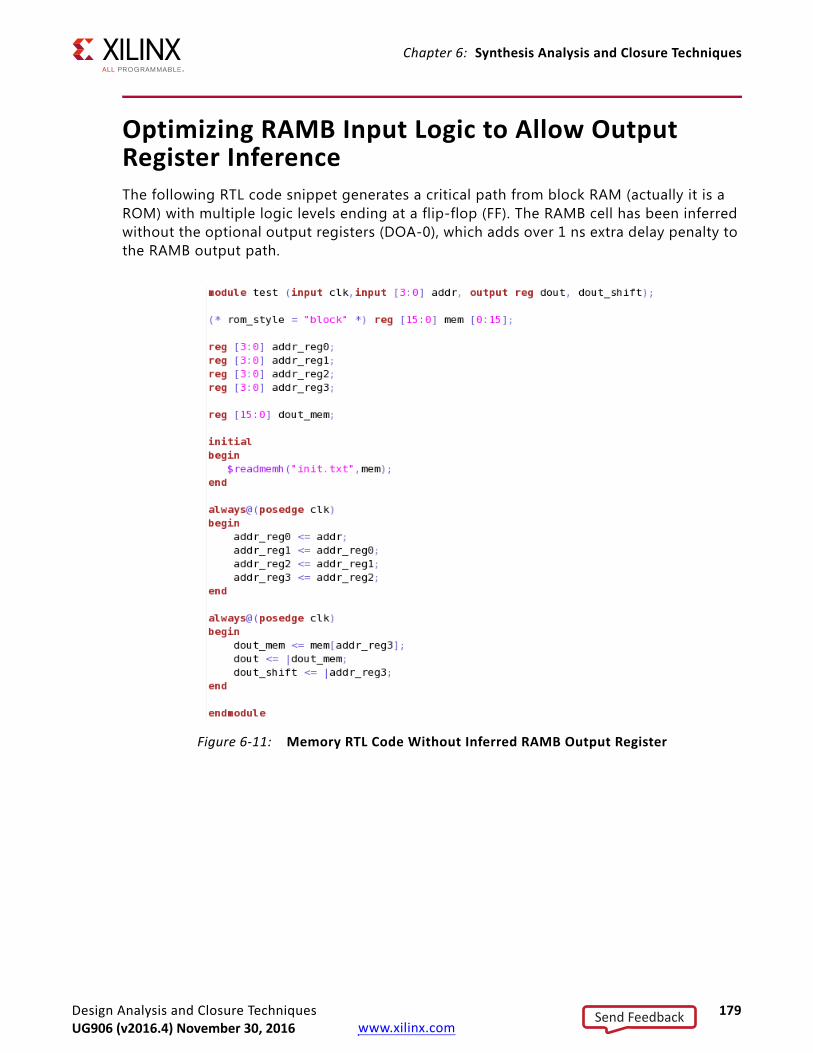
Design Analysis and Closure Techniques 179UG906 (v2016.3) October 5, 2016 www.xilinx.com
Chapter 6: Synthesis Analysis and Closure Techniques
Optimizing RAMB Input Logic to Allow Output Register InferenceThe following RTL code snippet generates a critical path from block RAM (actually it is a ROM) with multiple logic levels ending at a flip-flop (FF). The RAMB cell has been inferred without the optional output registers (DOA-0), which adds over 1 ns extra delay penalty to the RAMB output path.X-Ref Target - Figure 6-11
Figure 6-11: Memory RTL Code Without Inferred RAMB Output Register
Send FeedbackUG906 (v2016.4) November 30, 2016

Design Analysis and Closure Techniques 180UG906 (v2016.3) October 5, 2016 www.xilinx.com
Chapter 6: Synthesis Analysis and Closure Techniques
The critical path for the above RTL code is shown by the tool, such as in the following figure.
It is good practice to review the critical paths after synthesis and after each implementation step in order to identify which groups of logic need to be improved. For long paths or any paths that do not take advantage of the FPGA hardware features optimally, go back to the RTL description, try to understand why the synthesized logic is not optimal, and modify the code to help the synthesis tool improve the netlist.
Vivado has a powerful embedded debugging mechanism that you can use to start off with elaborated view. The elaborated view helps to identify where the problem could be, instead of manually searching through the RTL code. See the elaborated view shown in the following figure for the above RTL code snippet.
X-Ref Target - Figure 6-12
Figure 6-12: Critical Path from RAMB Without Output Register Enabled
X-Ref Target - Figure 6-13
Figure 6-13: Elaborated View of RTL Code Snippet
Send FeedbackUG906 (v2016.4) November 30, 2016

Design Analysis and Closure Techniques 181UG906 (v2016.3) October 5, 2016 www.xilinx.com
Chapter 6: Synthesis Analysis and Closure Techniques
The elaborated view gives a good hint about the inefficient structure for the given test case. In this case, the problem comes from the address register fanout (addr_reg3_reg), which drives the memory address as well as some glue-logic, highlighted in blue.
RAMB inference by the synthesis tool requires a dedicated address register in the RTL code, which is not compatible with the current address register fanout. As a consequence, the synthesis tool re-times the output register in order to allow the RAMB inference instead of using it to enable the RAMB optional output register.
By replicating the address register in the RTL code so that the memory address and the glue logic are driven by separate registers, the RAMB will be inferred with the output registers enabled.
The RTL code and elaborated view after manual replication are shown in the following figures:
X-Ref Target - Figure 6-14
Figure 6-14: RTL Code with the Replicated Address Register
Send FeedbackUG906 (v2016.4) November 30, 2016

Design Analysis and Closure Techniques 182UG906 (v2016.3) October 5, 2016 www.xilinx.com
Chapter 6: Synthesis Analysis and Closure Techniques
The critical path for the modified RTL code can be seen in the following figure Notice the following:
• The addr_reg2_reg register is connected to the address pin of the block RAM.
• The addr_reg3_reg register has been absorbed in the Block RAM.
• The RAMB output register is enabled, which significantly reduces the datapath delay on the RAMB outputs.
X-Ref Target - Figure 6-15
Figure 6-15: Elaborated View of the Replicated Address Register
X-Ref Target - Figure 6-16
Figure 6-16: Critical Path for the Modified RTL Code
Send FeedbackUG906 (v2016.4) November 30, 2016

Design Analysis and Closure Techniques 183UG906 (v2016.3) October 5, 2016 www.xilinx.com
Chapter 6: Synthesis Analysis and Closure Techniques
Improving Critical Logic on RAMB OutputsThe following test case highlights about improving critical paths through restructuring, such as when pushing macro (BRAM) closer to the destination register.
The following figure shows a 16x1 Multiplexer with only one input to the Multiplexer coming from BRAM and the rest of the inputs being fed by registers.
Critical path: BRAM-> 2 Logic levels -> FF.
X-Ref Target - Figure 6-17
Figure 6-17: 16x1 Multiplexer Connected to Block RAM Outputs
Send FeedbackUG906 (v2016.4) November 30, 2016

Design Analysis and Closure Techniques 184UG906 (v2016.3) October 5, 2016 www.xilinx.com
Chapter 6: Synthesis Analysis and Closure Techniques
The following figure shows the critical path where the BRAM to FF path is highlighted in red. There are 2 logic levels from BRAM->FF as well as FF->FF. Because BRAM CLK->Q delay is higher for BRAM, BRAM->FF is critical.
X-Ref Target - Figure 6-18
Figure 6-18: Critical RAMB-LUT-FF Path
Send FeedbackUG906 (v2016.4) November 30, 2016

Design Analysis and Closure Techniques 185UG906 (v2016.3) October 5, 2016 www.xilinx.com
Chapter 6: Synthesis Analysis and Closure Techniques
Next, look at the RTL code snippet shown in the following figure to see whether there is a way to restructure the logic.
The optimal way to restructure the logic is to rewrite the above code snippet by breaking the 16x1 Multiplexer into two multiplexers. You can exempt the condition of select value 4'd5 and use it as an enabling condition for the 2x1 Multiplexer as shown in Figure 6-20, creating this cascade Multiplexer structure results in FF->FF with 3 logic levels, but BRAM->FF is reduced to 1 logic level. This way, the BRAM->FF path has been improved, which helps the downstream tools for better placement because RAMB placement is more challenging than LUT and FF placement. In general, fewer long paths around Macro primitives such RAMB, FIFO, and DSP will yield better QoR for any given design
X-Ref Target - Figure 6-19
Figure 6-19: RTL Code Snippet
Send FeedbackUG906 (v2016.4) November 30, 2016

Design Analysis and Closure Techniques 186UG906 (v2016.3) October 5, 2016 www.xilinx.com
Chapter 6: Synthesis Analysis and Closure Techniques
X-Ref Target - Figure 6-20
Figure 6-20: Cascade Multiplexer Structure to Reduce RAMB Output Logic Levels
Send FeedbackUG906 (v2016.4) November 30, 2016

Design Analysis and Closure Techniques 187UG906 (v2016.3) October 5, 2016 www.xilinx.com
Chapter 7
Implementation Analysis and Closure Techniques
Using the report_design_analysis CommandWhen timing closure is difficult to achieve or when you are trying to improve the overall performance of your application, you must review the main characteristics of your design after running synthesis and after any step of the implementation flow. It is relatively easy to gather the high-level metrics such as timing summary numbers (WNS/TNS/WHS/THS) (report_timing_summary) or various resource utilization numbers (report_utilization, report_clock_utilization, report_high_fanout_nets and report_control_sets). But it is more difficult to analyze and identify which particular aspect of your design is impacting a specific timing path and consequently the overall Quality of Result (QoR). The QoR analysis usually requires you to look at several global and local characteristics at the same time to figure out what is suboptimal in the design and the constraints, or which logic structure is not suitable for the target device architecture and implementation tools. The report_design_analysis command gathers logical, timing and physical characteristics in a few tables that can simplify the QoR root cause analysis.
Note: The report_design_analysis command does not report on the completeness and correctness of timing constraints. To verify your timing constraints, you must use the check_timing and report_exceptions commands, as well as the XDC and TIMING methodology DRCs. For more information on how to run these commands, see the corresponding sections:
• Report Timing Summary, page 20
• Report Exceptions, page 60
Two main categories of QoR problems are usually encountered:
• Timing Violations
• Congestion
Send FeedbackUG906 (v2016.4) November 30, 2016

Design Analysis and Closure Techniques 188UG906 (v2016.3) October 5, 2016 www.xilinx.com
Chapter 7: Implementation Analysis and Closure Techniques
Timing ViolationsWhile analyzing and fixing the worst timing violation usually helps the overall QoR improvement, you must also review the other critical paths as they often contribute to the timing closure challenge. You can use the following command to report the 50 worst setup timing paths:
report_design_analysis -max_paths 50 -setup
Figure 7-1 shows an example of the Setup Path Characteristics table generated by this command.
From the table, you can isolate which characteristics are introducing the timing violation for each path:
• High logic delay percentage (Logic Delay)
° Are there many levels of logic? (LOGIC_LEVELS)
° Are there any constraints or attributes that prevent logic optimization? (Dont Touch, Mark Debug)
° Does the path include a cell with high logic delay such as RAMB or DSP?
° Is the path requirement too tight for the current path topology? (Requirement)
• High net delay percentage (Net Delay)
° Are there any high fanout nets in the path? (High Fanout, Cumulative Fanout)
° Are the cells assigned to several pblocks that can be placed far apart? (PBlocks)
° Are the cells placed far apart? (Bounding Box Size, Clock Region Distance)
° For SSI devices, are there nets crossing SLR boundaries? (SLR Crossings)
° Are one or several net delay values a lot higher than expected while the placement seems correct? See the section on Congestion, page 190.
X-Ref Target - Figure 7-1
Figure 7-1: Setup Path Characteristics
Send FeedbackUG906 (v2016.4) November 30, 2016
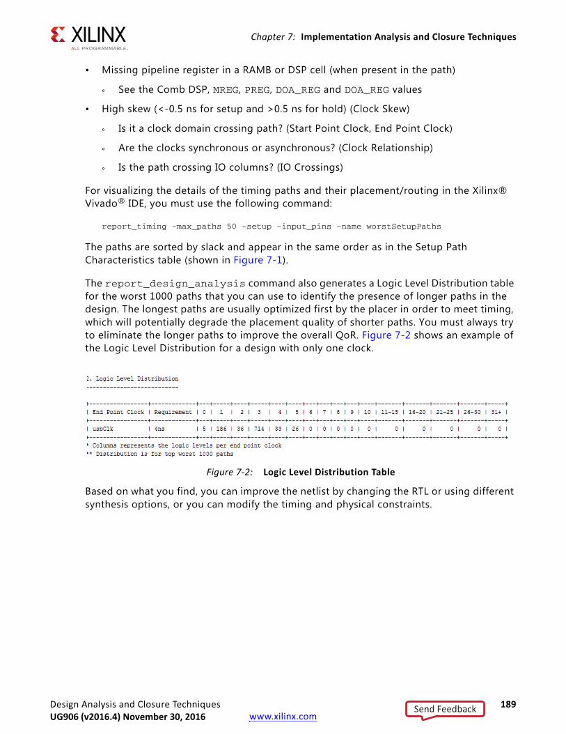
Design Analysis and Closure Techniques 189UG906 (v2016.3) October 5, 2016 www.xilinx.com
Chapter 7: Implementation Analysis and Closure Techniques
• Missing pipeline register in a RAMB or DSP cell (when present in the path)
° See the Comb DSP, MREG, PREG, DOA_REG and DOA_REG values
• High skew (<-0.5 ns for setup and >0.5 ns for hold) (Clock Skew)
° Is it a clock domain crossing path? (Start Point Clock, End Point Clock)
° Are the clocks synchronous or asynchronous? (Clock Relationship)
° Is the path crossing IO columns? (IO Crossings)
For visualizing the details of the timing paths and their placement/routing in the Xilinx® Vivado® IDE, you must use the following command:
report_timing -max_paths 50 -setup -input_pins -name worstSetupPaths
The paths are sorted by slack and appear in the same order as in the Setup Path Characteristics table (shown in Figure 7-1).
The report_design_analysis command also generates a Logic Level Distribution table for the worst 1000 paths that you can use to identify the presence of longer paths in the design. The longest paths are usually optimized first by the placer in order to meet timing, which will potentially degrade the placement quality of shorter paths. You must always try to eliminate the longer paths to improve the overall QoR. Figure 7-2 shows an example of the Logic Level Distribution for a design with only one clock.
Based on what you find, you can improve the netlist by changing the RTL or using different synthesis options, or you can modify the timing and physical constraints.
X-Ref Target - Figure 7-2
Figure 7-2: Logic Level Distribution Table
Send FeedbackUG906 (v2016.4) November 30, 2016

Design Analysis and Closure Techniques 190UG906 (v2016.3) October 5, 2016 www.xilinx.com
Chapter 7: Implementation Analysis and Closure Techniques
CongestionThe report_design_analysis command reports several congestion tables which show the congested area seen by the placer and router algorithms, as well as the estimated congestion. You can generate these tables using the following command in the same Vivado tools session where the placer and router were run:
report_design_analysis -congestion
Figure 7-3 shows an example of the estimated congestion tables which are equivalent to the Vertical and Horizontal Routing congestion per CLB metrics available in the Vivado IDE. In this example, the congestion is low.
The names provided for the Module Names correspond to the hierarchical cells present in each reported Tile. You can retrieve the complete name using the following command:
get_cells -hier <moduleName>
Once the hierarchical cells present in the congested area are identified, you can use congestion alleviating techniques to try reducing the overall design congestion.
X-Ref Target - Figure 7-3
Figure 7-3: Estimated Congestion Tables
Send FeedbackUG906 (v2016.4) November 30, 2016
Design Analysis and Closure Techniques 191UG906 (v2016.3) October 5, 2016 www.xilinx.com
Chapter 7: Implementation Analysis and Closure Techniques
Identifying the Longest Logic Delay Paths in the DesignTiming paths correspond to logical paths in the design. Their delay is the accumulation of cell delays and net delays. The Vivado synthesis and implementation tools are timing-driven and work on optimizing the worst violating paths of your design throughout the compilation flow. If accumulated cell delay for a path is equal to or higher than the timing requirement (for example, usually the clock period of the path), the design is unlikely to meet timing after implementation. Analyzing the logic delay is better than simply counting logic levels, because it shows what the worst paths are before estimated or routed net delays become a factor. The result of this analysis is a list of the worst timing paths before placement and routing, and without net delay.
It is important to identify the paths that are the worst in terms of timing and not necessarily levels of logic. For example, unregistered block RAM have very large clock to out delay, while a series of carry chains may have multiple levels of levels of logic, each with a small delay. You must analyze these paths carefully before implementation. There are three typical categories for these long delay paths:
• block RAMs that do not take advantage of the embedded output register
• DSP48s that are not pipelined
• Long logic paths
The most efficient method of identifying these long paths is to run a timing report post synthesis with the routing estimates set to none. This can be done by changing the Interconnect model to none in the Timer Settings tab of the Vivado IDE Timing Report dialog box, or by using the following Tcl command in the Tcl console or shell:
set_delay_model -interconnect none
Review the timing results to identify any failing paths. If there are paths that fail to meet timing without any routing delay, these paths will be impossible to meet timing with actual routing. These paths MUST be addressed immediately. Typically, these would have to be fixed in RTL, but the violations could also be due to missing synthesis attributes, or incorrect timing constraints. After implementing the changes, the design will have sufficient slack as shown in Figure 7-4.
Send FeedbackUG906 (v2016.4) November 30, 2016

Design Analysis and Closure Techniques 192UG906 (v2016.3) October 5, 2016 www.xilinx.com
Chapter 7: Implementation Analysis and Closure Techniques
Identifying High Fanout Net DriversHigh fanout nets often lead to implementation issues. As die sizes increase with each FPGA family, fanout problems also increase. It is often difficult to meet timing on nets that have many thousands of endpoints, especially if there is additional logic on the paths, or if they are driven from non-sequential cells, such as LUTs or distributed RAMs.
Many times, designers address the high fanout nets in RTL or synthesis by using a global fanout limit or a MAX_FANOUT attribute on a specific net. Physical optimization (phys_opt_design) automatically replicates the high fanout net drivers based on slack and placement information, and usually significantly improves timing. Xilinx recommends that you drive high fanout nets with a fabric register (FD*), which is easier to replicate and relocate during physical optimization. It is important to look at the list of high fanout signals post synthesis as well as post physical optimization. The command to identify these nets is report_high_fanout_nets.
Once the report has been generated, the timing through the high fanout nets and corresponding schematic can be reviewed. This report does not list clocks as the high fanout driver. If a BUFG is in the Driver Type column, this BUFG is driving logic and possibly also clock pins.
### Report the high fanout netreport_high_fanout_nets -load_types -max_nets 100### Report timing through specific high fanout netreport_timing -through [get_nets I_GLOBAL_RST_N_i] -name high_fanout_1
Following is an example of a design in which phys_opt_design was able to reduce the fanout:
Post Place Checkpoint: report_high_fanout_nets
X-Ref Target - Figure 7-4
Figure 7-4: Timing Report with 0 Interconnect
Send FeedbackUG906 (v2016.4) November 30, 2016
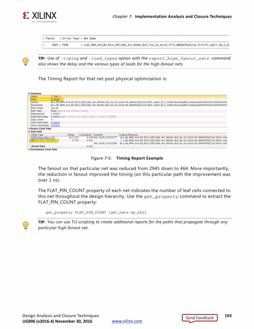
Design Analysis and Closure Techniques 193UG906 (v2016.3) October 5, 2016 www.xilinx.com
Chapter 7: Implementation Analysis and Closure Techniques
TIP: Use of -timing and -load_types option with the report_high_fanout_nets command also shows the delay and the various types of loads for the high-fanout nets.
The Timing Report for that net post physical optimization is:
The fanout on that particular net was reduced from 2945 down to 464. More importantly, the reduction in fanout improved the timing (on this particular path the improvement was over 1 ns).
The FLAT_PIN_COUNT property of each net indicates the number of leaf cells connected to this net throughout the design hierarchy. Use the get_property command to extract the FLAT_PIN_COUNT property:
get_property FLAT_PIN_COUNT [get_nets my_hfn]
TIP: You can use Tcl scripting to create additional reports for the paths that propagate through any particular high fanout net.
X-Ref Target - Figure 7-5
Figure 7-5: Timing Report Example
Send FeedbackUG906 (v2016.4) November 30, 2016

Design Analysis and Closure Techniques 194UG906 (v2016.3) October 5, 2016 www.xilinx.com
Chapter 7: Implementation Analysis and Closure Techniques
Determining if Hold-Fixing is Negatively Impacting the DesignThe Vivado Design Suite router prioritizes fixing hold over setup. This is because your design may work in the lab if you are failing setup by a small amount. There is always the option of lowering the clock frequency. If you have hold violations, the design will most likely not work.
In most cases, the router can meet the hold timing without affecting the setup. In some cases (mostly due to errors in the design or the constraints), the setup time will be significantly affected. Improper hold checks are often caused by improper set_multicycle_path constraints in which the -hold was not specified. In other cases, large hold requirements are due to excessive clock skew. In this case, Xilinx recommends that you review the clocking architecture for that particular circuit. For more information, see this link in the UltraFast Design Methodology Guide for the Vivado Design Suite (UG949) [Ref 5].
This may occur if your design meets setup timing post placement, but fails set up post route.
TIP: Analyze the estimated hold timing post place and identify any unusually large hold violations (over 500ps).
If you suspect that hold fixing is affecting timing closure, you can use one of the following to determine if this is the case:
• Method 1: Routing without hold fixing
• Method 2: Run report_timing -min on Worst Failing Setup Path
Method 1: Routing without hold fixing
1. Read the post-placed checkpoint into Vivado Design Suite.
2. Add a constraint to disable all hold checking:
set_false_path -hold -to [all_clocks]
CAUTION! This constraint is for test purposes only. Never do this for designs that will be put into production or delivered to another designer. You must remove this constraint before the production design.
3. Run route_design and report_timing_summary.
If there is a significant difference between the WNS with and without the hold checks, the hold violations might be too large, and the setup paths are being affected.
Send FeedbackUG906 (v2016.4) November 30, 2016

Design Analysis and Closure Techniques 195UG906 (v2016.3) October 5, 2016 www.xilinx.com
Chapter 7: Implementation Analysis and Closure Techniques
Method 2: Run report_timing -min on Worst Failing Setup Path
To determine whether the worst failing setup path is due to hold fixing, review the hold timing of that path. In the Vivado IDE, right click and report timing on source to destination. As opposed to doing the setup timing analysis, it is important to look at the hold timing. Once you have the hold report, verify the requirement and ensure that additional delay was not added on the path to be able to meet hold.
X-Ref Target - Figure 7-6
Figure 7-6: Running Timing Report on Specific Paths
Send FeedbackUG906 (v2016.4) November 30, 2016

Design Analysis and Closure Techniques 196UG906 (v2016.3) October 5, 2016 www.xilinx.com
Chapter 7: Implementation Analysis and Closure Techniques
Quickly Analyzing All Failing PathsThe report_timing_summary command is a powerful tool for determining all the timing information for your design. Sometimes it is beneficial to simply look at all of the failing paths in a single report. The command below works from the command line or from within the IDE.
report_timing -max_paths 100 -slack_less_than 0 -name worse_100_setup
TIP: When using the IDE, you can export the timing results to a spreadsheet to do more comprehensive analysis of the failing paths.
The command above reports the top 100 failing paths. If there are less than 100 failing paths, only the failing paths are reported because of the -slack_less_than 0 option. Reviewing the failing paths in a single list helps to quickly identify the order of magnitude differences among the failing paths.
For example, the WNS could be -3 ns, which affects a few paths, but then the next WNS in the list could be at -300 ps or better.
By default, when you analyze timing failures, you see the single worst timing path per endpoint. There are generally many similar paths for the common failing endpoint.
To review all worst paths for a single endpoint, use the -nworst option with the report_timing command. For example, run the following command to see all paths leading to the worst case failing endpoint (assuming there are less than 100):
report_timing -max_paths 100 -nworst 100
Reviewing all the worst paths may yield considerable data. To minimize the amount of data to analyze, you can review only the unique portions of paths by using the -unique_pins option with the report_timing command. This provides a single path for each unique combination of pins through the timing path. For example:
report_timing -max_paths 100 -nworst 100 -unique_pins
Send FeedbackUG906 (v2016.4) November 30, 2016

Design Analysis and Closure Techniques 197UG906 (v2016.3) October 5, 2016 www.xilinx.com
Chapter 7: Implementation Analysis and Closure Techniques
FloorplanningThis section discusses Floorplanning and includes:
• About Floorplanning
• Understanding Floorplanning Basics
• Using Pblock-Based Floorplanning
• Locking Specific Logic to Device Sites
• Floorplanning With Stacked Silicon Interconnect (SSI) Devices
About FloorplanningFloorplanning can help a design meet timing. Xilinx recommends that you floorplan when a design does not meet timing consistently, or has never met timing.
Floorplanning is also helpful when you are working with design teams, and consistency is most important.
Floorplanning can improve the setup slack (TNS, WNS) by reducing the average route delay. During implementation, the timing engine works on resolving the worst setup violations and all the hold violations. Floorplanning can only improve setup slack.
Manual floorplanning is easiest when the netlist has hierarchy. Design analysis is much slower when synthesis flattens the entire netlist. Set up synthesis to generate a hierarchical netlist. For Vivado synthesis use:
• synth_design -flatten_hierarchy rebuilt
or
• The Vivado Synthesis Defaults strategy
Large hierarchical blocks with intertwined logical paths can be difficult to analyze. It is easier to analyze a design in which separate logical structures are in lower sub-hierarchies. Consider registering all the outputs of a hierarchical module. It is difficult to analyze the placement of paths that trace through multiple hierarchical blocks.
Send FeedbackUG906 (v2016.4) November 30, 2016

Design Analysis and Closure Techniques 198UG906 (v2016.3) October 5, 2016 www.xilinx.com
Chapter 7: Implementation Analysis and Closure Techniques
Understanding Floorplanning BasicsNot every design will always meet timing. You may have to guide the tools to a solution. Floorplanning allows you to guide the tools, either through high-level hierarchy layout, or through detailed gate placement.
You will achieve the greatest improvements by fixing the worst problems or the most common problems. For example if there are outlier paths that have significantly worse slack, or high levels of logic, fix those paths first. The Tools > Timing > Create Slack Histogram command can provide a view of outlier paths. Alternatively, if the same timing endpoint appears in several negative slack paths, improving one of the paths might result in similar improvements for the other paths on that endpoint.
Consider floorplanning to increase performance by reducing route delay or increasing logic density on a non-critical block. Logic density is a measure of how tightly the logic is packed onto the chip.
Floorplanning can help you meet a higher clock frequency and improve consistency in the results.
There are multiple approaches to floorplanning, each with its advantages and disadvantages.
Detailed Gate-Level Floorplanning
Detailed gate-level floorplanning involves placing individual leaf cells in specific sites on the device.
Advantages of Detailed Gate-Level Floorplanning
• Detailed gate-level floorplanning works with hand routing nets.
• Detailed gate-level floorplanning can extract the most performance out of the device.
Disadvantages of Detailed Gate-Level Floorplanning
• Detailed gate-level floorplanning is time consuming.
• Detailed gate-level floorplanning requires extensive knowledge of the device and design.
• Detailed gate-level floorplanning may need to be redone if the netlist changes.
RECOMMENDED: Use detailed gate-level floorplanning as a last resort.
Send FeedbackUG906 (v2016.4) November 30, 2016

Design Analysis and Closure Techniques 199UG906 (v2016.3) October 5, 2016 www.xilinx.com
Chapter 7: Implementation Analysis and Closure Techniques
Information Reuse
Reuse information from a design that met timing. Use this flow if the design does not consistently meet timing. To reuse information:
1. Open two implementation runs:
a. One for a run that is meeting timing.
b. One for a run that is not meeting timing.
TIP: On a computer with multiple monitors, select Open Implementation in New Window to open a design in a new window.
2. Look for the differences between the two designs.
a. Identify some failing timing paths from report_timing_summary.
b. On the design that is meeting timing, run report_timing in min_max mode to time those same paths on the design that meets timing.
3. Compare the timing results:
a. Clock skew
b. Datapath delay
c. Placement
d. Route delays
4. If there are differences in the amount of logic delay between path end points, revisit the synthesis runs.
Review I/O and Cell Placement
Review the placement of the cells in the design. Compare two I/O reports to review the I/O placement and I/O standards. Make sure all the I/Os are placed. A simple search finds all I/Os without fixed placement as shown in the following figure.
Send FeedbackUG906 (v2016.4) November 30, 2016
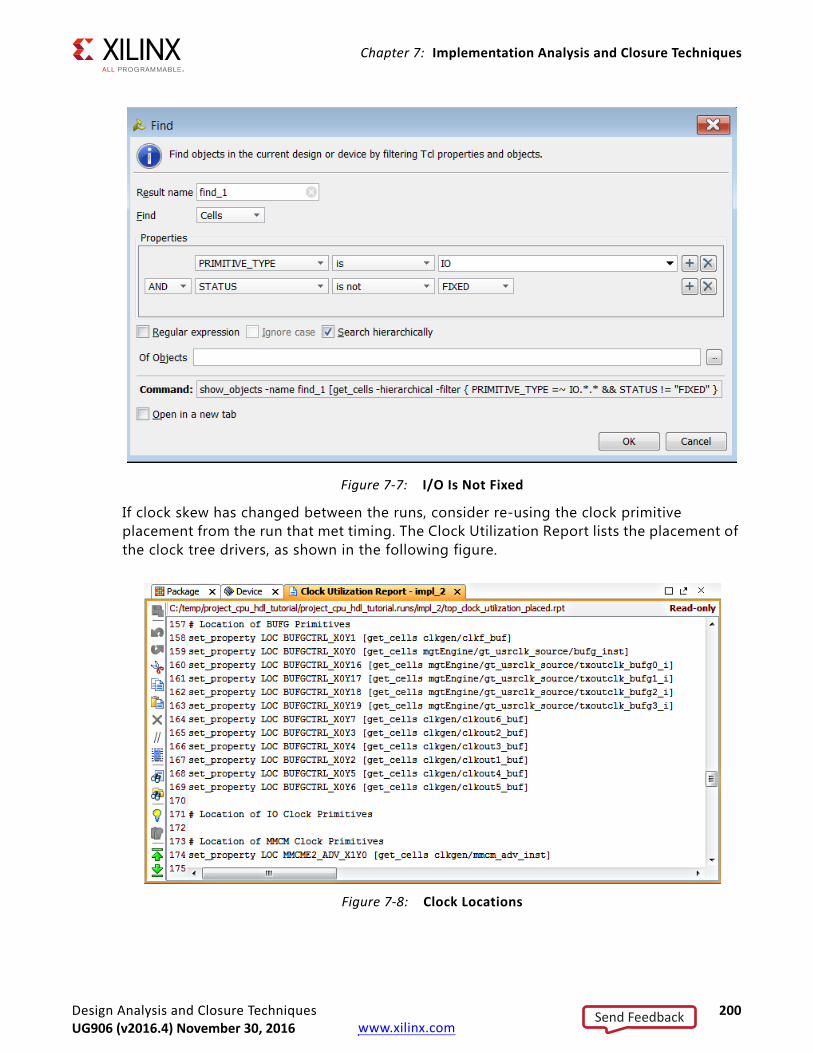
Design Analysis and Closure Techniques 200UG906 (v2016.3) October 5, 2016 www.xilinx.com
Chapter 7: Implementation Analysis and Closure Techniques
If clock skew has changed between the runs, consider re-using the clock primitive placement from the run that met timing. The Clock Utilization Report lists the placement of the clock tree drivers, as shown in the following figure.
X-Ref Target - Figure 7-7
Figure 7-7: I/O Is Not Fixed
X-Ref Target - Figure 7-8
Figure 7-8: Clock Locations
Send FeedbackUG906 (v2016.4) November 30, 2016

Design Analysis and Closure Techniques 201UG906 (v2016.3) October 5, 2016 www.xilinx.com
Chapter 7: Implementation Analysis and Closure Techniques
The LOC constraints can easily be copied into your XDC constraints file.
Many designs have met timing by reusing the placement of the Block RAMs and DSPs. Select Edit > Find to list the instances.
Adding Placement Constraints
Fix the logic to add the placement constraints to your XDC.
1. Select the macros from the find results.
2. Right click and select Fix Cells (shown in the following figure).
X-Ref Target - Figure 7-9
Figure 7-9: DSP or RAM
Send FeedbackUG906 (v2016.4) November 30, 2016

Design Analysis and Closure Techniques 202UG906 (v2016.3) October 5, 2016 www.xilinx.com
Chapter 7: Implementation Analysis and Closure Techniques
RECOMMENDED: Analyze the placement based on hierarchy name and highlight before fixing the placement.
Reusing PlacementIt is fairly easy to reuse the placement of I/Os, Global Clock Resources, BlockRAM macros, and DSP macros.
Re-using this placement helps to reduce the variability in results from one netlist revision to the next. These primitives generally have stable names. The placement is usually easy to maintain.
TIP: Do not reuse the placement of general slice logic. Do not reuse the placement for sections of the design that are likely to change.
Floorplanning TechniquesConsider gate-level floorplanning for a design that has never met timing, and in which changing the netlist or the constraints are not good options.
RECOMMENDED: Try hierarchical floorplanning before considering gate level floorplanning.
X-Ref Target - Figure 7-10
Figure 7-10: Selecting the Logic to Fix
Send FeedbackUG906 (v2016.4) November 30, 2016

Design Analysis and Closure Techniques 203UG906 (v2016.3) October 5, 2016 www.xilinx.com
Chapter 7: Implementation Analysis and Closure Techniques
Hierarchical Floorplanning
Hierarchical floorplanning allows you to place one or more levels of hierarchy in a region on the chip. This region provides guidance to the placer at a global level, and the placer does the detailed placement. Hierarchical floorplanning has the following advantages over gate-level floorplanning:
• Hierarchical floorplan creation is fast compared to gate-level floorplanning. A good floorplan can improve timing. The floorplan is resistant to design change.
• The level of hierarchy acts as a container for all the gates. It will generally work if the netlist changes.
In hierarchical floorplanning:
• Identify the lower levels of hierarchy that contain the critical path.
• Use the top level floorplan to identify where to place them.
• Implementation places individual cells.
• Has comprehensive knowledge of the cells and timing paths.
• Generally does a good job of fine grain placement.
Manual Cell Placement
Manual cell placement can obtain the best performance from a device. When using this technique, designers generally use it only on a small block of the design. They may hand place a small amount of logic around a high speed I/O interface, or hand place Block RAMs and DSPs. Manual placement can be slow.
All floorplanning techniques can require significant engineering time. They might require floorplan iterations. If any of the cell names change, the floorplan constraints must be updated.
When floorplanning, you should have an idea of final pinout. It is useful to have the I/Os fixed. The I/Os can provide anchor points for starting the floorplan. Logic that communicates to I/Os migrates towards the fixed pins.
TIP: Place blocks that communicate with I/Os near their I/Os. If the pinout is pulling a block apart, consider pinout or RTL modification.
Send FeedbackUG906 (v2016.4) November 30, 2016
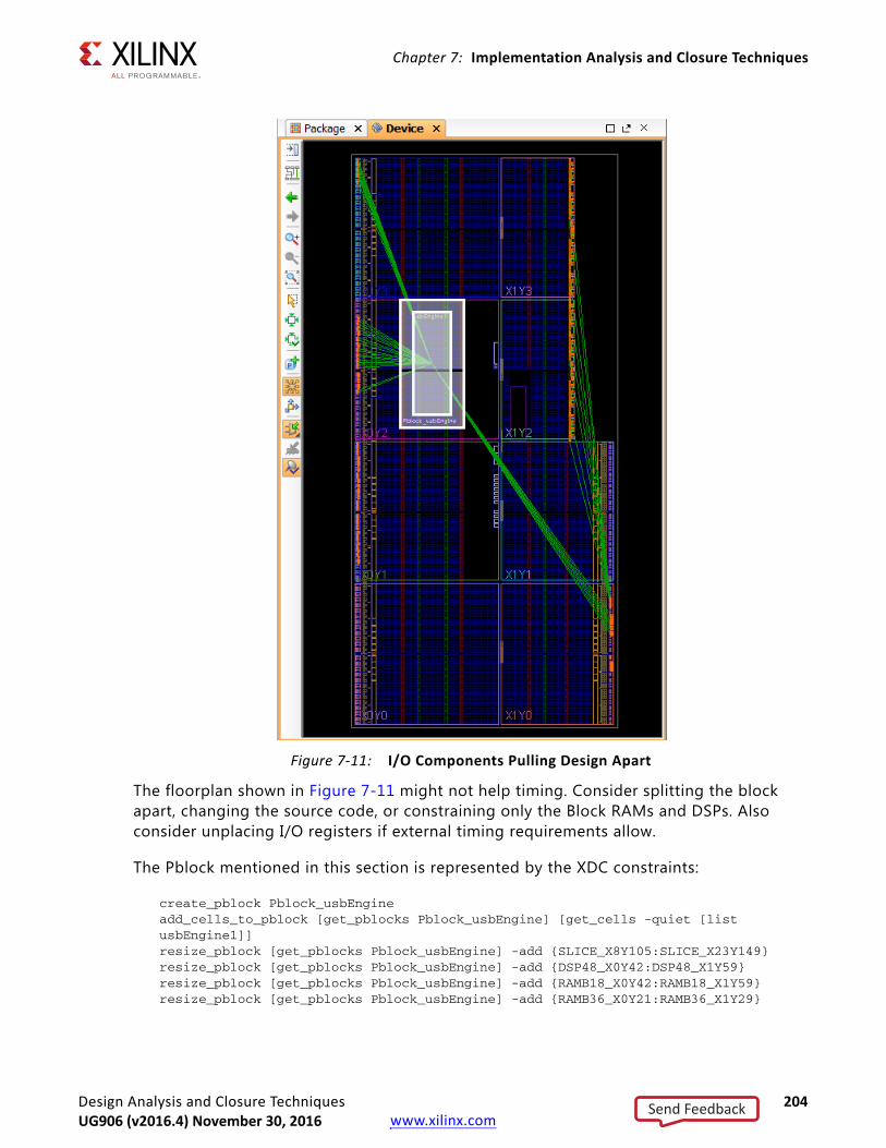
Design Analysis and Closure Techniques 204UG906 (v2016.3) October 5, 2016 www.xilinx.com
Chapter 7: Implementation Analysis and Closure Techniques
The floorplan shown in Figure 7-11 might not help timing. Consider splitting the block apart, changing the source code, or constraining only the Block RAMs and DSPs. Also consider unplacing I/O registers if external timing requirements allow.
The Pblock mentioned in this section is represented by the XDC constraints:
create_pblock Pblock_usbEngineadd_cells_to_pblock [get_pblocks Pblock_usbEngine] [get_cells -quiet [list usbEngine1]] resize_pblock [get_pblocks Pblock_usbEngine] -add {SLICE_X8Y105:SLICE_X23Y149} resize_pblock [get_pblocks Pblock_usbEngine] -add {DSP48_X0Y42:DSP48_X1Y59} resize_pblock [get_pblocks Pblock_usbEngine] -add {RAMB18_X0Y42:RAMB18_X1Y59} resize_pblock [get_pblocks Pblock_usbEngine] -add {RAMB36_X0Y21:RAMB36_X1Y29}
X-Ref Target - Figure 7-11
Figure 7-11: I/O Components Pulling Design Apart
Send FeedbackUG906 (v2016.4) November 30, 2016

Design Analysis and Closure Techniques 205UG906 (v2016.3) October 5, 2016 www.xilinx.com
Chapter 7: Implementation Analysis and Closure Techniques
The first line creates the Pblock. The second line (add_cells_to_pblock) assigns the level of hierarchy to the Pblock. There are four resource types (SLICE, DSP48, RAMB18, RAMB36) each with its own grid. Logic that is not constrained by a grid can go anywhere in the device. To constrain just the Block RAMs in the level of hierarchy, disable the other Pblock grids.
The resulting XDC commands define the simplified Pblock:
create_pblock Pblock_usbEngineadd_cells_to_pblock [get_pblocks Pblock_usbEngine] [get_cells -quiet [list usbEngine1]] resize_pblock [get_pblocks Pblock_usbEngine] -add {RAMB18_X0Y42:RAMB18_X1Y59} resize_pblock [get_pblocks Pblock_usbEngine] -add {RAMB36_X0Y21:RAMB36_X1Y29}
The Block RAMs are constrained in the device, but the slice logic is free to be placed anywhere on the device.
TIP: When placing Pblocks, be careful not to floorplan hierarchy in such a manner that it crosses the central config block.
X-Ref Target - Figure 7-12
Figure 7-12: Pblock Grids
Send FeedbackUG906 (v2016.4) November 30, 2016

Design Analysis and Closure Techniques 206UG906 (v2016.3) October 5, 2016 www.xilinx.com
Chapter 7: Implementation Analysis and Closure Techniques
Using Pblock-Based FloorplanningWhen you integrate RTL into a design, it helps to visualize the design inside the device. Graphically seeing how the blocks interconnect between themselves and the I/O pinout after synthesis helps you to understand your design.
To view the interconnect, generate a top level floorplan using Pblocks on upper levels of hierarchy. To break apart the top level RTL into Pblocks, select Tools > Floorplanning > Auto Create Pblocks.
To place the blocks in the device, select Tools > Floorplanning > Place Pblocks. The tool sizes the Pblocks based on the slice count and target utilization.
X-Ref Target - Figure 7-13
Figure 7-13: Avoiding the Config Block
Send FeedbackUG906 (v2016.4) November 30, 2016

Design Analysis and Closure Techniques 207UG906 (v2016.3) October 5, 2016 www.xilinx.com
Chapter 7: Implementation Analysis and Closure Techniques
Pblocks can be more than one hundred percent full during analysis, but not during implementation. Overfilling the Pblock makes them smaller on the device. This is a useful technique for getting an overview of the relative size of your design top-level blocks, and how they will occupy the device.
Top-Level Floorplan
The top-level floorplan shows which blocks communicate with I/Os (green lines). Nets connecting two Pblocks are bundled together. The bundles change size and color based on the number of shared nets. Two top-level floorplans are shown in Figure 7-15 and Figure 7-16.
The Data Path Top Level Floorplan shows how the data flows between the top-level blocks of the design. Each block communicates only with two neighbors. The green lines show well-placed I/Os that communicate with a single block.
X-Ref Target - Figure 7-14
Figure 7-14: Place Pblocks Utilization
Send FeedbackUG906 (v2016.4) November 30, 2016

Design Analysis and Closure Techniques 208UG906 (v2016.3) October 5, 2016 www.xilinx.com
Chapter 7: Implementation Analysis and Closure Techniques
The Control Path Floorplan displays a design in which all the blocks communicate with a central block. The largest connection is between the central block and the block in the bottom right. The central block must spread out around the design to communicate with all the other loads.
X-Ref Target - Figure 7-15
Figure 7-15: Data Path Top Level Floorplan
Send FeedbackUG906 (v2016.4) November 30, 2016

Design Analysis and Closure Techniques 209UG906 (v2016.3) October 5, 2016 www.xilinx.com
Chapter 7: Implementation Analysis and Closure Techniques
Reviewing the Floorplan
Consider device resources when reviewing the floorplan. The Pblock sizing does not take into account specialized device resources such as:
• Block RAM
• DSP48s
• MGTs
• ClockBuffers
TIP: Review the blocks with the floorplan and utilization in mind.
X-Ref Target - Figure 7-16
Figure 7-16: Control Path Floorplan
Send FeedbackUG906 (v2016.4) November 30, 2016

Design Analysis and Closure Techniques 210UG906 (v2016.3) October 5, 2016 www.xilinx.com
Chapter 7: Implementation Analysis and Closure Techniques
Locking Specific Logic to Device SitesYou can place cells on specific locations on the FPGA device, such as placing all the I/O ports on a Xilinx 7 series FPGA design. Xilinx recommends that you place the I/Os before attempting to close timing.
The I/O placement can impact the cell placement in the FPGA fabric. Hand placing other cells in the fabric can help provide some consistency to clock logic and macro placement, with the goal of more consistent implementation runs.
Fixed and Unfixed Cells
Fixed and Unfixed apply to placed cells. They describe the way in which the Vivado tools view placed cells in the design.
For more information about Fixed and Unfixed Cells, refer to this link in the Vivado Design Suite User Guide: Implementation (UG904) [Ref 7].
RECOMMENDED: After the I/Os are placed, use a hierarchical Pblock floorplan as a starting point for user-controlled placement. Hand placing logic should be used when Pblocks have been found not to work.
Floorplanning With Stacked Silicon Interconnect (SSI) DevicesThere are extra considerations for Stacked Silicon Interconnect (SSI) parts. The SSI parts are made of multiple Super Logic Regions (SLRs), joined by an interposer. The interposer connections are called Super Long Lines (SLLs). There is some delay penalty when crossing from one SLR to another.
Keep the SLRs in mind when structuring the design, generating a pinout, and floorplanning. Minimize SLL crossings by keeping logic cells of critical timing paths inside a single SLR.
Table 7-1: Constraints Used to Place Logic
Constraint Use Notes
LOC Places a gate or macro at a specific site.
SLICE sites have subsites called BEL sites.
BEL Specifies the subsite in the slice to use for a basic element.
Send FeedbackUG906 (v2016.4) November 30, 2016

Design Analysis and Closure Techniques 211UG906 (v2016.3) October 5, 2016 www.xilinx.com
Chapter 7: Implementation Analysis and Closure Techniques
The I/Os must be placed in the same SLR as the relevant I/O interface circuitry. You must also carefully consider clock placement when laying out logic for SSI parts.
RECOMMENDED: Let the placer try an automatic placement of the logic into the SSI parts before doing extensive partitioning. Analyzing the automatic placement may suggest floorplanning approaches you were not considering.
X-Ref Target - Figure 7-17
Figure 7-17: Minimize SLR Crossings
Send FeedbackUG906 (v2016.4) November 30, 2016

Design Analysis and Closure Techniques 212UG906 (v2016.3) October 5, 2016 www.xilinx.com
Appendix A
Timing Methodology Checks
TIMING-1: Invalid Clock Waveform on Clock Modifying BlockInvalid clock waveform for clock <CLOCK_NAME> specified at a <CELL_TYPE> output <PIN_NAME> that does not match the Clock Modifying Block (CMB) settings. The waveform of the clock is <VALUE>. The expected waveform is <VALUE>.
DescriptionThe Xilinx® Vivado® Design Suite automatically derives clocks on the output of a CMB based on the CMB settings and the characteristics of the incoming master clock. If the user defines a generated clock on the output of the CMB, Vivado does not auto-derive a generated clock on the same definition point (net or pin). The DRC warning is reporting that the user-defined generated clock does not match the expected auto-derived clock that Vivado would automatically create. This could lead to hardware failures because the timing constraints for the design do not match what happens on the device.
ResolutionIf the user-defined generated clock is unnecessary, remove the constraint and use the auto-derived clock instead. If constraint is necessary, verify that the generated clock constraint matches the auto-derived clock waveform or modify the CMB properties to match the expected clock waveform. If the intention is to force the name of the auto-derived clock, the recommendation is to use the create_generated_clock constraint with only the -name option defined and the name of the object where the clock is defined (typically output pin of CMB). See the Vivado Design Suite User Guide: Using Constraints (UG903) [Ref 6] for additional information about creating generated clocks and restrictions of the auto-derived clocks renaming constraint.
Send FeedbackUG906 (v2016.4) November 30, 2016
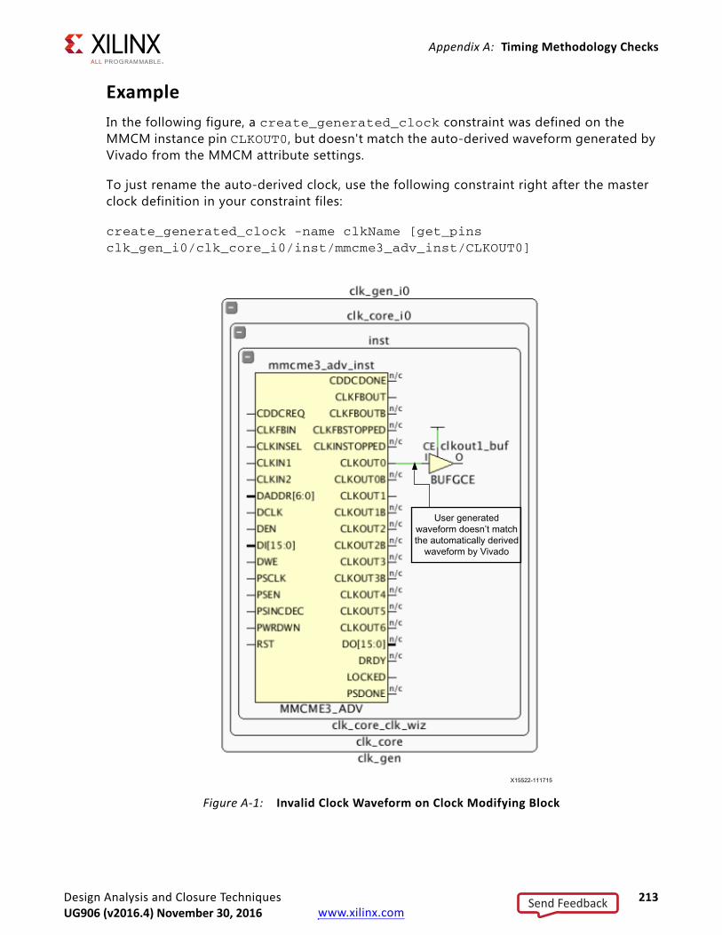
Design Analysis and Closure Techniques 213UG906 (v2016.3) October 5, 2016 www.xilinx.com
Appendix A: Timing Methodology Checks
ExampleIn the following figure, a create_generated_clock constraint was defined on the MMCM instance pin CLKOUT0, but doesn't match the auto-derived waveform generated by Vivado from the MMCM attribute settings.
To just rename the auto-derived clock, use the following constraint right after the master clock definition in your constraint files:
create_generated_clock -name clkName [get_pins clk_gen_i0/clk_core_i0/inst/mmcme3_adv_inst/CLKOUT0]
X-Ref Target - Figure A-1
Figure A-1: Invalid Clock Waveform on Clock Modifying Block
Send FeedbackUG906 (v2016.4) November 30, 2016

Design Analysis and Closure Techniques 214UG906 (v2016.3) October 5, 2016 www.xilinx.com
Appendix A: Timing Methodology Checks
TIMING-2: Invalid Primary Clock on Internal PinA primary clock <CLOCK_NAME> is created on an inappropriate pin <PIN_NAME>. It is recommended to create a primary clock only on a proper clock root (input port or primitive output pin with no timing arc).
DescriptionA primary clock must be defined on the source of the clock tree. For example, this would be the input port of the design. When a primary clock is defined in the middle of a logic path, timing analysis can become inaccurate because it ignores the insertion delay prior to the primary clock source point, which prevents proper skew computation. Therefore, a primary clock created on an internal driver pin should be discouraged. The consequence could be a failure in hardware.
ResolutionModify the create_clock constraint to use the actual clock tree source.
ExampleIn the following figure, the primary clock definition, create_clock constraint, was placed on the output pin of the IBUFCTRL instance. If the clock clk_pin_p is used to time an input or output port path, the slack will be inaccurate because part of the clock tree insertion delay will be missing. The primary clock definition for the differential input buffer should be placed on the top-level port clk_pin_p.X-Ref Target - Figure A-2
Figure A-2: Invalid Primary Clock on Internal Pin
Send FeedbackUG906 (v2016.4) November 30, 2016

Design Analysis and Closure Techniques 215UG906 (v2016.3) October 5, 2016 www.xilinx.com
Appendix A: Timing Methodology Checks
TIMING-3: Invalid Primary Clock on Clock Modifying BlockA primary clock <CLOCK_NAME> is created on the output pin or net <PIN/NET_NAME> of a Clock Modifying Block.
DescriptionVivado automatically derives clocks on the output of a CMB based on the CMB settings and the characteristics of the incoming master clock. If the user defines a primary clock on the output of the CMB, Vivado does not auto-derive a clock on the same output. This DRC is reporting that a primary clock was created on the output of the CMB, which breaks the relationship with the incoming clock and prevents proper clock insertion delay computation. This is not recommended because it can lead to inaccurate timing analysis and incorrect hardware behavior.
ResolutionModify the constraints to remove the create_clock constraint on the output of the CMB. If the intention is to force the name of the auto-generated clock, Xilinx recommends using the create_generated_clock constraint with only the -name option and the CMB output pin. See the Vivado Design Suite User Guide: Using Constraints (UG903) [Ref 6] for additional information about creating generated clocks.
ExampleIn the following figure, a create_clock constraint was defined on the MMCM instance pin CLKOUT0. This overrides the automatically derived clock created by Vivado and loses any relationship with the incoming clock.
To just rename the auto-derived clock, use the following constraint right after the master clock definition in your constraint files:
create_generated_clock -name clkName [get_pins clk_gen_i0/clk_core_i0/inst/mmcme3_adv_inst/CLKOUT0]
Send FeedbackUG906 (v2016.4) November 30, 2016

Design Analysis and Closure Techniques 216UG906 (v2016.3) October 5, 2016 www.xilinx.com
Appendix A: Timing Methodology Checks
X-Ref Target - Figure A-3
Figure A-3: Invalid Primary Clock on Clock Modifying Block
Send FeedbackUG906 (v2016.4) November 30, 2016
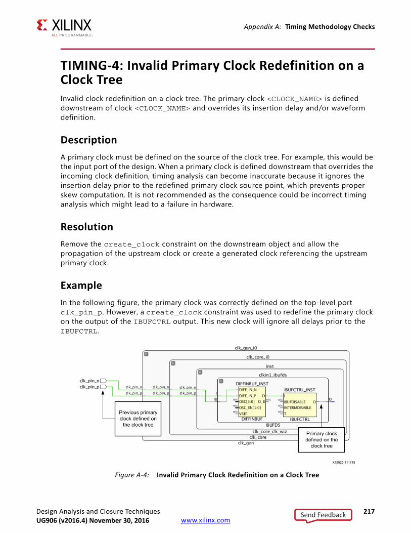
Design Analysis and Closure Techniques 217UG906 (v2016.3) October 5, 2016 www.xilinx.com
Appendix A: Timing Methodology Checks
TIMING-4: Invalid Primary Clock Redefinition on a Clock TreeInvalid clock redefinition on a clock tree. The primary clock <CLOCK_NAME> is defined downstream of clock <CLOCK_NAME> and overrides its insertion delay and/or waveform definition.
DescriptionA primary clock must be defined on the source of the clock tree. For example, this would be the input port of the design. When a primary clock is defined downstream that overrides the incoming clock definition, timing analysis can become inaccurate because it ignores the insertion delay prior to the redefined primary clock source point, which prevents proper skew computation. It is not recommended as the consequence could be incorrect timing analysis which might lead to a failure in hardware.
ResolutionRemove the create_clock constraint on the downstream object and allow the propagation of the upstream clock or create a generated clock referencing the upstream primary clock.
ExampleIn the following figure, the primary clock was correctly defined on the top-level port clk_pin_p. However, a create_clock constraint was used to redefine the primary clock on the output of the IBUFCTRL output. This new clock will ignore all delays prior to the IBUFCTRL.X-Ref Target - Figure A-4
Figure A-4: Invalid Primary Clock Redefinition on a Clock Tree
Send FeedbackUG906 (v2016.4) November 30, 2016
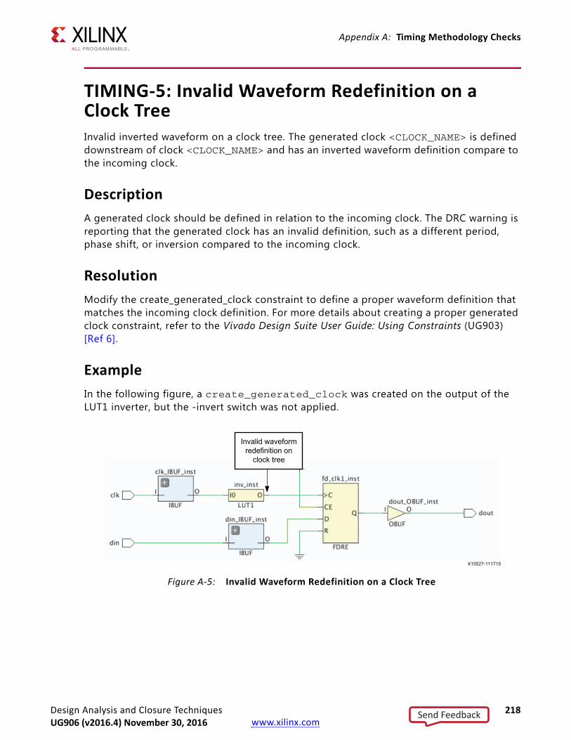
Design Analysis and Closure Techniques 218UG906 (v2016.3) October 5, 2016 www.xilinx.com
Appendix A: Timing Methodology Checks
TIMING-5: Invalid Waveform Redefinition on a Clock TreeInvalid inverted waveform on a clock tree. The generated clock <CLOCK_NAME> is defined downstream of clock <CLOCK_NAME> and has an inverted waveform definition compare to the incoming clock.
DescriptionA generated clock should be defined in relation to the incoming clock. The DRC warning is reporting that the generated clock has an invalid definition, such as a different period, phase shift, or inversion compared to the incoming clock.
ResolutionModify the create_generated_clock constraint to define a proper waveform definition that matches the incoming clock definition. For more details about creating a proper generated clock constraint, refer to the Vivado Design Suite User Guide: Using Constraints (UG903) [Ref 6].
ExampleIn the following figure, a create_generated_clock was created on the output of the LUT1 inverter, but the -invert switch was not applied.X-Ref Target - Figure A-5
Figure A-5: Invalid Waveform Redefinition on a Clock Tree
Send FeedbackUG906 (v2016.4) November 30, 2016

Design Analysis and Closure Techniques 219UG906 (v2016.3) October 5, 2016 www.xilinx.com
Appendix A: Timing Methodology Checks
TIMING-6: No Common Primary Clock Between Related ClocksThe clocks <CLOCK_NAME1> and <CLOCK_NAME2> are related (timed together) but they have no common primary clock. The design could fail in hardware even if timing is met. To find a timing path between these clocks, run the following command: report_timing -from [get_clocks <CLOCK_NAME1>] -to [get_clocks <CLOCK_NAME2>].
DescriptionThe two clocks reported are considered related and timed as synchronous by default even if they are not derived from a common primary clock and do not have a known phase relationship. The DRC warning is reporting that the timing engine cannot guarantee that these clocks are synchronous.
ResolutionThe resolution depends on whether the two clock domains are asynchronous or synchronous. In the case of the clocks being asynchronous, the paths between the two domains should be covered by a timing exception (such as set_max_delay -datapath_only, set_clock_groups, or set_false_path). The DRC will be resolved once all the paths between these two domains have full exception coverage.
ExampleIn the case of the clocks being synchronous, you can define one timing clock on both clock source objects if originally both clocks have the same waveform (see the first example below).
Example 1: create_clock -period 10 -name clk1 [get_ports <clock-1-source> <clock-2-source>]
If the two clocks have different waveforms, you can define the first clock as a primary clock and the second clock as a generated clock, with the first clock specified as the master clock (see Example 2 below).
Example 2: create_clock -period 10 -name clk1 [get_ports <clock-1-source>]
If the clocks are related, but have a clock period ratio of 2, the solution is to create a primary clock on the one source, and create a generated clock on the second source:
create_generated_clock -source [get_ports <clock-1-source>] -name clk2 -divide_by 2 [get_ports <clock-2-source>]
Send FeedbackUG906 (v2016.4) November 30, 2016

Design Analysis and Closure Techniques 220UG906 (v2016.3) October 5, 2016 www.xilinx.com
Appendix A: Timing Methodology Checks
TIMING-7: No Common Node Between Related ClocksThe clocks <CLOCK_NAME1> and <CLOCK_NAME2> are related (timed together) but they have no common node. The design could fail in hardware. To find a timing path between these clocks, run the following command: report_timing -from [get_clocks <CLOCK_NAME1>] -to [get_clocks <CLOCK_NAME2>].
DescriptionThe two clocks reported are considered related and timed as synchronous by default. The DRC warning is reporting that the timing engine cannot guarantee that these clocks are synchronous in hardware, since it could not determine a common node between the two clock trees.
ResolutionThe resolution depends on whether the two clock domains are asynchronous or synchronous. In the case of the clocks being asynchronous, the paths between the two domains should be covered by a timing exception (such as set_max_delay -datapath_only, set_clock_groups, or set_false_path).
In the case of the clocks being synchronous, this DRC warning can be waived.
ExampleIn the following figure, a synchronous clock domain crossing (CDC) exists between the clk1 and clk2 domains. Both clk1 and clk2 are determined to be synchronous in Vivado by default. However, since clk1 and clk2 are input ports, there is no common node relationship between the two clocks. For this case, Vivado cannot guarantee that the two clocks are synchronous.X-Ref Target - Figure A-6
Figure A-6: No Common Node Between Related Clocks
Send FeedbackUG906 (v2016.4) November 30, 2016

Design Analysis and Closure Techniques 221UG906 (v2016.3) October 5, 2016 www.xilinx.com
Appendix A: Timing Methodology Checks
TIMING-8: No Common Period Between Related ClocksThe clocks <CLOCK_NAME1> and <CLOCK_NAME2> are found related (timed together) but have no common (expandable) period.
DescriptionThe two clocks reported are considered related and timed as synchronous by default. However, the timing engine was unable to determine a common period after expanding the waveform of both clocks over 1000 cycles. In such a case, the worst setup relationship over these 1000 cycles is used for timing analysis. However, the timing engine cannot ensure this is the most pessimistic case. This typically occurs with clocks with an odd fractional period ratio.
ResolutionAs the waveforms do not allow safe timing analysis between the two clocks, it is recommended to treat these clocks as asynchronous. Therefore, the paths between the two clock domains should be covered by a timing exception (such as set_max_delay -datapath_only, set_false_path, or set_clock_groups).
Send FeedbackUG906 (v2016.4) November 30, 2016

Design Analysis and Closure Techniques 222UG906 (v2016.3) October 5, 2016 www.xilinx.com
Appendix A: Timing Methodology Checks
TIMING-9: Unknown CDC LogicAn asynchronous Clock Domain Crossing has been detected between clock <CLOCK_NAME1> and clock <CLOCK_NAME2> through a set_false_path or a set_clock_groups or a set_max_delay -datapath_only constraint but no safe CDC logic has been identified (crossing pin <PIN_NAME>).
DescriptionThe purpose of the DRC is to ensure that inter-clock domains constrained with timing exceptions have been designed with safe asynchronous clock domain crossing circuitry. For more details on recognized safe topologies, see Report Clock Domain Crossings, page 66.
ResolutionThe recommendation is to make the appropriate design to have a proper synchronization for the inter-clock paths. To do this, add, at minimum, a double-register logic synchronizer. In the case a FIFO or higher-level protocol is already defined on the path, this DRC can be safely ignored.
ExampleIn the following figure, an asynchronous clock domain exists between clk1 and clk2. However, the clk2 capture domain doesn't contain a double register logic synchronizer to synchronize the data.X-Ref Target - Figure A-7
Figure A-7: Missing Synchronizer
Send FeedbackUG906 (v2016.4) November 30, 2016

Design Analysis and Closure Techniques 223UG906 (v2016.3) October 5, 2016 www.xilinx.com
Appendix A: Timing Methodology Checks
TIMING-10: Missing Property on SynchronizerA logic synchronizer with <CELL_NAME1> and <CELL_NAME2> has been detected between clock <CLOCK_NAME1> and clock <CLOCK_NAME2> but the synchronizer does not have the property ASYNC_REG=TRUE on both registers.
DescriptionSynchronizer registers must have their ASYNC_REG property set to TRUE in order to preserve the cells through any logic optimization during synthesis and implementation, and to optimize their placement for the best mean time between failure (MTBF) statistics.
ResolutionThe solution is to add the ASYNC_REG constraint to each stage of the logic synchronizer. To find out more information on the ASYNC_REG constraint, refer to the Vivado Design Suite Properties Reference Guide (UG912) [Ref 10].
ExampleIn the following figure, an asynchronous clock domain exists between clk1 and clk2 and is properly synchronized with a double register logic synchronizer. However, each register of the synchronizer needs to have the ASYNC_REG property applied to increase the timing slack and lower MTBF.X-Ref Target - Figure A-8
Figure A-8: Missing Property on Synchronizer
Send FeedbackUG906 (v2016.4) November 30, 2016

Design Analysis and Closure Techniques 224UG906 (v2016.3) October 5, 2016 www.xilinx.com
Appendix A: Timing Methodology Checks
TIMING-11: Inappropriate Max Delay with Datapath Only OptionA max delay constraint with -datapath_only has been applied between <PIN_NAME> and <PIN_NAME>. The startpoint(s) and endpoint(s) either belong to the same clock domain or belong to two clock domains that can safely be timed together. It is only recommended to use the -datapath_only option on paths between clocks that do not have a known phase relationship. This DRC is waived when a synchronizer is found on the path endpoint.
DescriptionThe set_max_delay with the -datapath_only option is used to remove the clock skew from the setup slack computation and to ignore hold timing. The set_max_delay -datapath_only command is used to constrain asynchronous signals timing paths that: (1) do not have a clock relationship; but which (2) require maximum delay. It is not recommended to use this constraint on synchronous paths.
ResolutionThe solution is to modify the set_max_delay -datapath_only constraint such that it does not cover synchronous timing paths. Refer to the startpoint and endpoint cells listed in the message to find the associated set_max_delay constraint.
Send FeedbackUG906 (v2016.4) November 30, 2016

Design Analysis and Closure Techniques 225UG906 (v2016.3) October 5, 2016 www.xilinx.com
Appendix A: Timing Methodology Checks
TIMING-12: Clock Reconvergence Pessimism Removal Disabled
DescriptionThe Clock Reconvergence Pessimism Removal (CRPR) mode has been disabled. It is not recommended to perform timing analysis in this mode as over-pessimistic clock tree delays could result in impossible timing closure.
The CRPR feature is used to remove artificially induced pessimism that is derived from the usage of the maximum and minimum delay along the common portion of the clock network. If the CRPR is disabled, it might be difficult to close timing.
ResolutionThe recommendation is to enable the CRPR analysis to ensure the design has accurate timing information. The Tcl command to enable the CRPR analysis is config_timing_pessimism -enable.
TIMING-13: Timing Paths Ignored Due to Path SegmentationSome timing paths are not reported due to path segmentation on pin(s) <PIN_NAME>. To prevent path segmentation, all the Min and Max delay constraints should be defined with a list of valid startpoints and endpoints.
DescriptionPath segmentation occurs when a timing path is broken into a smaller path to be timed. When max and min delay constraints are defined on pins that are invalid startpoints (and respectively, endpoints), the timing engine breaks the timing arcs going through the node so that the node becomes a valid startpoint (and respectively, endpoint). It is highly recommended to avoid path segmentation as it might have unexpected consequences. This might result in incorrect timing analysis and hardware failures.
ResolutionAvoid path segmentation whenever possible by carefully choosing valid startpoints and endpoints in the set_max_delay and set_min_delay constraints. For additional information on path segmentation and using the Min/Max delay constraints, refer to the Vivado Design Suite User Guide: Using Constraints (UG903) [Ref 6].
Send FeedbackUG906 (v2016.4) November 30, 2016

Design Analysis and Closure Techniques 226UG906 (v2016.3) October 5, 2016 www.xilinx.com
Appendix A: Timing Methodology Checks
TIMING-14: LUT on the Clock TreeThe LUT <CELL_NAME> has been found on the clock tree. It is not recommended to have LUT cells on the clock path.
DescriptionA LUT on the clock path might cause excess skew because the clock must be routed on general routing resources through the fabric. In addition to excess skew, these paths are more susceptible to PVT variations. It is highly recommended to avoid local clocks whenever possible.
ResolutionThe solution is to change the design to remove the LUT located on the clock tree. Synthesis can create this situation in many cases such as clock gating and inversion. In the case of an inversion LUT1 cell, the LUT might be absorbed into the downstream SLICE after opt_design. Investigate the case to ensure that the situation is still valid after opt_design is complete.
ExampleIn the following figure, a LUT is used to gate the clock with a clock enable signal. The LUT on the path can cause excess skew, which is undesirable.X-Ref Target - Figure A-9
Figure A-9: LUT on the Clock Tree
Send FeedbackUG906 (v2016.4) November 30, 2016

Design Analysis and Closure Techniques 227UG906 (v2016.3) October 5, 2016 www.xilinx.com
Appendix A: Timing Methodology Checks
TIMING-15: Large Hold Violation on Inter-Clock PathThere is a large inter-clock skew of <VALUE> ns between <CELL_NAME> (clocked by <CLOCK_NAME>) and <CELL_NAME> (clocked by <CLOCK_NAME>) that results in large hold timing violation(s) of <VALUE> ns. Fixing large hold violations during routing might impact setup slack and result in more difficult timing closure.
DescriptionThe DRC warning is reporting that the large hold violation due to the inter-clock skew will most likely be difficult to close timing during implementation. It is recommended to investigate the large inter-clock skew greater than 1.0 ns to ensure proper constraints or design topology.
ResolutionInvestigate whether the large inter-clock skew on the timing path should be timed or is related to non-optimal timing constraints. If the large skew occurs due to an unconstrained CDC path, add the necessary timing exception. If the violation occurs due to a logic associated with the clock tree, investigate the topology of path for improvements to more easily close timing.
Send FeedbackUG906 (v2016.4) November 30, 2016

Design Analysis and Closure Techniques 228UG906 (v2016.3) October 5, 2016 www.xilinx.com
Appendix A: Timing Methodology Checks
TIMING-16: Large Setup ViolationThere is a large setup violation of <VALUE> ns between <CELL_NAME> (clocked by <CLOCK_NAME>) and <CELL_NAME> (clocked by <CLOCK_NAME>). Large setup violations at the end of those stages might be difficult to fix during the post-placement implementation flow and could be the result of non-optimal XDC constraints or non-optimal design architecture.
DescriptionThis DRC warning reports setup violations that will most likely be difficult to close timing during implementation. It is recommended to investigate setup violations greater than 1.0 ns to ensure proper constraints or design topologies.
ResolutionInvestigate whether the large setup violation is a timing path that should be timed or is related to non-optimal timing constraints. If the setup violation occurs due to an unconstrained CDC path, add the necessary timing exception. If the violation occurs due to a significant amount of combinational logic, investigate the topology of the path for improvements to more easily close timing.
Send FeedbackUG906 (v2016.4) November 30, 2016

Design Analysis and Closure Techniques 229UG906 (v2016.3) October 5, 2016 www.xilinx.com
Appendix A: Timing Methodology Checks
TIMING-17: Non-Clocked Sequential CellThe clock pin <PIN_NAME> is not reached by a timing clock.
DescriptionThe DRC reports the list of sequential cells unconstrained by a timing clock which affect the resulting timing analysis for the reported cells. It is highly recommended that all clocks be properly defined in order to get the maximum timing path coverage with the best accuracy. The consequence could be missing timing analysis, which might lead to hardware failures.
ResolutionThe resolution is to create the missing primary or generated clock on the clock tree driving the unconstrained sequential cells.
TIMING-18: Missing Input or Output DelayAn <INPUT/OUTPUT> delay is missing on <PORT_NAME> relative to clock(s) <CLOCK_NAME>.
DescriptionIO timing is in reference to a timing path that includes an external device. The input and output delays specify the paths delay of the ports relative to a clock edge at the interface of the design. It is highly recommended to add input/output delay constraints to ensure that the FPGA interface can meet the timing of the external devices.
ResolutionAdd the required input and output delay constraints in correspondence with required board application.
Send FeedbackUG906 (v2016.4) November 30, 2016
Design Analysis and Closure Techniques 230UG906 (v2016.3) October 5, 2016 www.xilinx.com
Appendix A: Timing Methodology Checks
TIMING-19: Inverted Generated Clock Waveform on ODDRThe waveform of the generated clock <CLOCK_NAME> is inverted compared to the waveform of the incoming clock <CLOCK_NAME>.
DescriptionA generated clock on a forwarded clock port should be defined in relation to the incoming clock. The DRC warning is reporting that the generated clock on the forwarding clock port has an invalid waveform, such as an inversion, compared to the incoming source clock. This might lead to hardware failures as the timing analysis of the ports associated with the forwarded clock do not match what happens on the device.
ResolutionModify the create_generated_clock constraint to define a proper waveform that matches the incoming clock definition. For more details about creating a proper generated clock constraint, refer to the Vivado Design Suite User Guide: Using Constraints (UG903) [Ref 6].
TIMING-20: Non-Clocked LatchThe latch <CELL_NAME> cannot be properly analyzed because its control pin <PIN_NAME> is not reached by a timing clock.
DescriptionThis DRC is reporting the list of latch cells not constrained by a timing clock which affect the resulting timing analysis. It is highly recommended that all clocks be properly defined in order to get the maximum timing path coverage with the best accuracy. The consequence could be incomplete timing analysis coverage, which might lead to hardware failures.
ResolutionThe resolution is to create the primary or generated clock on the source of the clock tree driving the unconstrained control pins on the latch cells.
Send FeedbackUG906 (v2016.4) November 30, 2016

Design Analysis and Closure Techniques 231UG906 (v2016.3) October 5, 2016 www.xilinx.com
Appendix A: Timing Methodology Checks
TIMING-21: Invalid COMPENSATION Property on MMCMThe MMCM <CELL_NAME> has an invalid COMPENSATION property value relative to the connection of its feedback loop. If the feedback loop goes outside the FPGA, the property should be set to EXTERNAL. If the feedback loop is internal to the FPGA, the property should be set to ZHOLD.
DescriptionMMCM compensation modes define how the MMCM feedback is configured for delay compensation of the output clocks. Depending on the MMCM use case, the feedback path should match a specific topology. This DRC warning is reporting that the topology of the MMCM use case doesn't match the COMPENSATION property value. This might lead to unintended behavior in hardware because the timing analysis does not match.
ResolutionThe recommendation is to leave the default value of AUTO to the COMPENSATION property of the MMCM in the design. The Vivado Integrated Design Environment (IDE) will automatically select the appropriate compensation value based on the circuit topology. For additional information on the compensation property and the input delay compensation, refer to the Clocking Resources User Guide for your specific architecture.
Send FeedbackUG906 (v2016.4) November 30, 2016

Design Analysis and Closure Techniques 232UG906 (v2016.3) October 5, 2016 www.xilinx.com
Appendix A: Timing Methodology Checks
TIMING-22: Missing External Delay on MMCMThe MMCM <CELL_NAME> has an external feedback loop but no external delay has been specified between FBOUT and FBIN. It is recommended to specify an external delay with set_external_delay between the two ports connected to the pins FBOUT and FBIN with an external feedback loop.
DescriptionThe MMCM can be configured for external deskew where the feedback board trace matches the trace to the external components. The external delay value is used in the calculation of the MMCM compensation delay. This could lead to hardware failures, especially on the IO paths, because the timing analysis of the MMCM compensation does not match what happens on the device.
ResolutionAdd a set_external_delay constraint between the external feedback input and output port for the defined external trace delay. For additional information on the set_external_delay command, refer to the Vivado Design Suite Tcl Command Reference Guide (UG835) [Ref 3].
Exampleset_external_delay -from <output_port> -to <input_port> <external_delay_value>
Send FeedbackUG906 (v2016.4) November 30, 2016

Design Analysis and Closure Techniques 233UG906 (v2016.3) October 5, 2016 www.xilinx.com
Appendix A: Timing Methodology Checks
TIMING-23: Combinatorial Loop FoundA timing loop has been detected on a combinational path. A timing arc has been disabled between <CELL_NAME1> and <CELL_NAME2> to break the timing loop.
DescriptionCombinatorial timing loops are created when the output of combinatorial logic is fed back to its input, resulting in a timing loop. This loop unnecessarily increases the number of cycles by infinitely going around the same path and cannot be timed. To resolve the timing loop, the Vivado IDE disables the timing arc on the cell in the loop.
ResolutionIf you didn't intend to create a combinatorial feedback loop, correct the issue by modifying the design source files (RTL). But because the timing loop is expected, use the set_disable_timing command to break the timing loop where it makes the most sense (usually the feedback path) instead of letting Vivado Timing break it at a random location.
TIMING-24: Overridden Max Delay Datapath OnlyA set_clock_groups or a set_false_path between clocks <CLOCK_NAME1> and <CLOCK_NAME2> overrides a set_max_delay -datapath_only (see constraint position <#> in the Timing Constraints window in the Vivado IDE). It is not recommended to override a set_max_delay -datapath_only constraint. Replace the set_clock_groups or set_false_path between clocks with point-to-point set_false_path constraints.
DescriptionThe DRC warning only occurs when a set_max_delay -datapath_only constraint is overridden by a set_clock_groups or set_false_path constraint between clocks. If a point-to-point set_false_path overrides a set_max_delay -datapath_only, the DRC will not be reported.
ResolutionThe solution is to replace the set_clock_groups or set_false_path between clocks with point-to-point false path constraints to avoid incorrectly overriding a set_max_delay -datapath_only constraint.
Send FeedbackUG906 (v2016.4) November 30, 2016

Design Analysis and Closure Techniques 234UG906 (v2016.3) October 5, 2016 www.xilinx.com
Appendix A: Timing Methodology Checks
TIMING-25: Invalid Clock Waveform on Gigabit Transceiver (GT)The waveform of the clock <CLOCK_NAME> defined on the transceiver output pin <PIN_NAME> or on the net connected to that pin is not consistent with the transceiver settings or the reference clock definition is missing. The auto-derived clock period is <PERIOD> and the user-defined clock period is <PERIOD>.
DescriptionFor UltraScale™ devices, Vivado automatically derives clocks on the output of a GT based on the GT settings and the characteristics of the incoming master clock. For 7 series devices, Vivado does not automatically derive the GT clocks; it is your responsibility to create the appropriate primary clocks on the GT's output pins. The DRC warning is reporting that the user-defined clock does not match the expected auto-derived clock that Vivado would automatically create. This could lead to hardware failures as the timing constraints for the design do not match what happens on the device.
ResolutionIf the user-defined generated clock is unnecessary, remove the constraint and use the auto-derived clock instead. If constraint is necessary, verify that the generated clock constraint matches the auto-derived clock waveform or modify the GT properties to match the expected clock waveform. If the intention is to force the name of the auto-derived clock, the recommendation is to use the create_generated_clock constraint with only the -name option defined and the name of the object where the clock is defined (typically output pin of GT). See the Vivado Design Suite User Guide: Using Constraints (UG903) [Ref 6] for additional information about creating generated clocks and restrictions of the auto-derived clocks renaming constraint.
Send FeedbackUG906 (v2016.4) November 30, 2016

Design Analysis and Closure Techniques 235UG906 (v2016.3) October 5, 2016 www.xilinx.com
Appendix A: Timing Methodology Checks
TIMING-26: Missing Clock on Gigabit Transceiver (GT)The output clock pin <PIN_NAME> does not have clock defined. Create a primary clock on the <PORT_NAME> input port in order to let Vivado auto-derive the missing GT clocks.
DescriptionFor UltraScale devices, Vivado automatically derives clocks on the output of a GT based on the GT settings and the characteristics of the incoming master clock. The DRC warning is reporting that Vivado is unable to auto-derive the output clock of the GT due to the missing primary clock on the input port. The consequence is that the downstream logic connected to the GT related clocks will not be timed.
ResolutionCreate a primary clock on the recommended input port to the GT.
TIMING-27: Invalid Primary Clock on Hierarchical PinA primary clock <CLOCK_NAME> is created on an inappropriate internal pin <PIN_NAME>. It is not recommended to create a primary clock on a hierarchical pin when its driver pin has a fanout connected to multiple clock pins.
DescriptionIf the driver is traversed by a clock and a new clock is defined downstream on a hierarchical pin, the cells downstream of the hierarchal pin will have different timing analysis compared to the cells on the fanout of the driver pin. If any synchronous paths exist between the driver clock and the hierarchical pin clock, skew will be inaccurate and timing signoff will be invalid. This situation can result in hardware failure.
ResolutionRemove the primary clock definition on the hierarchical pin, or if the downstream clock is absolutely needed, use a generated clock constraint with the driver clock specified as master clock instead.
Send FeedbackUG906 (v2016.4) November 30, 2016

Design Analysis and Closure Techniques 236UG906 (v2016.3) October 5, 2016 www.xilinx.com
Appendix A: Timing Methodology Checks
TIMING-28: Auto-Derived Clock Referenced by a Timing ConstraintThe auto-derived clock <CLOCK_NAME> is referenced by name inside timing constraint (see constraint position <#> in the Timing Constraint window in the Vivado IDE). It is recommended to reference an auto-derived clock by the pin name attached to the clock: get_clocks -of_objects [get_pins <PIN_NAME>].
DescriptionAn auto-derived clock should be referenced by the source pin object. The auto-derived clock name might change during development due to modifications to the netlist or constraints. Referencing an auto-derived clock by name should be discouraged, because the consequence could be invalidated constraints in subsequent runs after the design has been modified.
ResolutionModify the constraint to reference the auto-derived clock by the pin name attached to the clock using [get_clocks -of_objects [get_pins <PIN_NAME>]]. Alternatively, use the create_generated_clock constraint to force the name of the auto-derived clock. For more details about using a generated clock constraint to force a clock name, refer to the Vivado Design Suite User Guide: Using Constraints (UG903) [Ref 6].
Send FeedbackUG906 (v2016.4) November 30, 2016

Design Analysis and Closure Techniques 237UG906 (v2016.3) October 5, 2016 www.xilinx.com
Appendix A: Timing Methodology Checks
TIMING-29: Inconsistent Pair of Multicycle PathsSetup and hold multicycle path constraints should typically reference the same -start pair for SLOW-to-FAST synchronous clocks or -end pair for FAST-to-SLOW synchronous clocks (see constraint positions <#>, <#> in the Timing Constraint window in Vivado IDE).
DescriptionBy default, the set_multicycle_path constraint is used to modify the path requirement multipliers with respect to the source clock for hold or the destination clock for setup. For certain use cases, the path requirement must be multiplied with respect to a specific clock edge.
ResolutionFor both setup and hold, modify the set_multicycle_path constraints to reference the destination clock (-end) for SLOW-to-FAST synchronous clocks and the source clock (-start) for FAST-to-SLOW synchronous clocks. See the Vivado Design Suite User Guide: Using Constraints (UG903) [Ref 6] for additional information about properly setting multicycle paths between clocks.
Send FeedbackUG906 (v2016.4) November 30, 2016

Design Analysis and Closure Techniques 238UG906 (v2016.3) October 5, 2016 www.xilinx.com
Appendix A: Timing Methodology Checks
TIMING-30: Sub-Optimal Master Source Pin Selection for Generated ClockThe generated clock <CLOCK_NAME> has a sub-optimal master source pin selection, timing can be pessimistic.
DescriptionA generated clock should reference the clock that is propagating in its direct fanin, although the create_generated_clock command lets you specify any reference clock. This DRC warning is reporting that the generated clock is associated to a master clock defined farther upstream than the incoming master clock. In this situation, timing analysis can be more pessimistic and apply additional clock uncertainty on the paths between the master clock and the generated clock. This can lead to slightly more difficult timing closure. Is is recommended to associate the generated clock to the master clock source pin that the generated clock is derived.
ResolutionModify the create_generated_clock constraint to reference the master clock source pin from which the generated clock is directly derived in the design.
Send FeedbackUG906 (v2016.4) November 30, 2016
Design Analysis and Closure Techniques 239UG906 (v2016.3) October 5, 2016 www.xilinx.com
Appendix B
Additional Resources and Legal Notices
Xilinx ResourcesFor support resources such as Answers, Documentation, Downloads, and Forums, see Xilinx Support.
Solution CentersSee the Xilinx Solution Centers for support on devices, software tools, and intellectual property at all stages of the design cycle. Topics include design assistance, advisories, and troubleshooting tips.
Documentation Navigator and Design HubsXilinx Documentation Navigator provides access to Xilinx documents, videos, and support resources, which you can filter and search to find information. To open the Xilinx Documentation Navigator (DocNav):
• From the Vivado IDE, select Help > Documentation and Tutorials.
• On Windows, select Start > All Programs > Xilinx Design Tools > DocNav.
• At the Linux command prompt, enter docnav.
Xilinx Design Hubs provide links to documentation organized by design tasks and other topics, which you can use to learn key concepts and address frequently asked questions. To access the Design Hubs:
• In the Xilinx Documentation Navigator, click the Design Hubs View tab.
• On the Xilinx website, see the Design Hubs page.
Note: For more information on Documentation Navigator, see the Documentation Navigator page on the Xilinx website.
Send FeedbackUG906 (v2016.4) November 30, 2016

Design Analysis and Closure Techniques 240UG906 (v2016.3) October 5, 2016 www.xilinx.com
Appendix B: Additional Resources and Legal Notices
References The following Xilinx® Vivado® Design Suite documents provide supplemental material useful with this guide.
1. Vivado Design Suite User Guide: Using the Vivado IDE (UG893)
2. Vivado Design Suite User Guide: Using Tcl Scripting (UG894)
3. Vivado Design Suite Tcl Command Reference Guide (UG835)
4. Vivado Design Suite User Guide: System-Level Design Entry (UG895)
5. UltraFast Design Methodology Guide for the Vivado Design Suite (UG949)
6. Vivado Design Suite User Guide: Using Constraints (UG903)
7. Vivado Design Suite User Guide: Implementation (UG904)
8. Vivado Design Suite User Guide: Power Analysis and Optimization (UG907)
9. 7 Series Clocking Resources Guide (UG472)
10. Vivado Design Suite Properties Reference Guide (UG912)
11. All Vivado Design Suite Documentation
Training ResourcesXilinx provides a variety of training courses and QuickTake videos to help you learn more about the concepts presented in this document. Use these links to explore related training resources:
1. Vivado Design Suite QuickTake Video: UltraFast Vivado Design Methodology for Timing Closure
2. Vivado Design Suite QuickTake Video: Using the Vivado Timing Constraint Wizard
3. Vivado Design Suite QuickTake Video: Advanced Clock Constraints and Analysis
4. Vivado Design Suite QuickTake Video: Analyzing Implementation Results
5. Vivado Design Suite QuickTake Video: Running Design Rule Checks (DRCs) in Vivado
6. Vivado Design Suite QuickTake Video: Timing Analysis Controls
7. Vivado Design Suite QuickTake Video: Vivado Timing Closure Techniques - Physical Optimization
8. Vivado Design Suite QuickTake Video: Cross Clock Domain Checking - CDC Analysis
Send FeedbackUG906 (v2016.4) November 30, 2016

Design Analysis and Closure Techniques 241UG906 (v2016.3) October 5, 2016 www.xilinx.com
Appendix B: Additional Resources and Legal Notices
9. Vivado Design Suite QuickTake Video: Design Analysis and Floorplanning with Vivado
10. Vivado Design Suite QuickTake Video Tutorials
Please Read: Important Legal NoticesThe information disclosed to you hereunder (the “Materials”) is provided solely for the selection and use of Xilinx products. To the maximum extent permitted by applicable law: (1) Materials are made available "AS IS" and with all faults, Xilinx hereby DISCLAIMS ALL WARRANTIES AND CONDITIONS, EXPRESS, IMPLIED, OR STATUTORY, INCLUDING BUT NOT LIMITED TO WARRANTIES OF MERCHANTABILITY, NON-INFRINGEMENT, OR FITNESS FOR ANY PARTICULAR PURPOSE; and (2) Xilinx shall not be liable (whether in contract or tort, including negligence, or under any other theory of liability) for any loss or damage of any kind or nature related to, arising under, or in connection with, the Materials (including your use of the Materials), including for any direct, indirect, special, incidental, or consequential loss or damage (including loss of data, profits, goodwill, or any type of loss or damage suffered as a result of any action brought by a third party) even if such damage or loss was reasonably foreseeable or Xilinx had been advised of the possibility of the same. Xilinx assumes no obligation to correct any errors contained in the Materials or to notify you of updates to the Materials or to product specifications. You may not reproduce, modify, distribute, or publicly display the Materials without prior written consent. Certain products are subject to the terms and conditions of Xilinx’s limited warranty, please refer to Xilinx’s Terms of Sale which can be viewed at http://www.xilinx.com/legal.htm#tos; IP cores may be subject to warranty and support terms contained in a license issued to you by Xilinx. Xilinx products are not designed or intended to be fail-safe or for use in any application requiring fail-safe performance; you assume sole risk and liability for use of Xilinx products in such critical applications, please refer to Xilinx’s Terms of Sale which can be viewed at http://www.xilinx.com/legal.htm#tos.AUTOMOTIVE APPLICATIONS DISCLAIMERAUTOMOTIVE PRODUCTS (IDENTIFIED AS "XA" IN THE PART NUMBER) ARE NOT WARRANTED FOR USE IN THE DEPLOYMENT OF AIRBAGS OR FOR USE IN APPLICATIONS THAT AFFECT CONTROL OF A VEHICLE ("SAFETY APPLICATION") UNLESS THERE IS A SAFETY CONCEPT OR REDUNDANCY FEATURE CONSISTENT WITH THE ISO 26262 AUTOMOTIVE SAFETY STANDARD ("SAFETY DESIGN"). CUSTOMER SHALL, PRIOR TO USING OR DISTRIBUTING ANY SYSTEMS THAT INCORPORATE PRODUCTS, THOROUGHLY TEST SUCH SYSTEMS FOR SAFETY PURPOSES. USE OF PRODUCTS IN A SAFETY APPLICATION WITHOUT A SAFETY DESIGN IS FULLY AT THE RISK OF CUSTOMER, SUBJECT ONLY TO APPLICABLE LAWS AND REGULATIONS GOVERNING LIMITATIONS ON PRODUCT LIABILITY.© Copyright 2012-2016 Xilinx, Inc. Xilinx, the Xilinx logo, Artix, ISE, Kintex, Spartan, Virtex, Vivado, Zynq, and other designated brands included herein are trademarks of Xilinx in the United States and other countries. All other trademarks are the property of their respective owners.
Send FeedbackUG906 (v2016.4) November 30, 2016