Embed Size (px)
Citation preview
VME64 ExtensionsDraft Standard
VITA 1.1-199x
Draft 1.7May 5, 1997
This draft standard is being prepared by the VITAStandards Organization (VSO) and is unapproved.
Do not specify or claim conformanceto this draft standard.
VSO is the Public Domain Administrator of this draft standardand guards the contents from change except by sanctioned
meetings of the task group under due process.
VITA Standards Organization7825 East Gelding Drive, Suite 104
Scottsdale, AZ 85260Ph: 602-951-8866 Fx: 602-951-0720
URL: http://www.vita.com
Table of Contents, Abstract and Foreword
Do not specify or claim conformance to this draft standard
VME64x, VITA 1.1-199x/D1.7 ii 5/5/97
TABLE OF CONTENTS
Abstract .............................................................................................................................. vForeword ........................................................................................................................... vi
Chapter 1 ........................................................................................................................... 1Introduction to the VME64 Extensions Draft Standard ..................................................... 11.1 VME64 Extensions Objectives ................................................................................... 1
1.1.1 9U Boards, Backplanes and Subracks ............................................................ 21.2 Terminology ............................................................................................................... 21.3 References ................................................................................................................. 2
1.3.1 Connector Notes .............................................................................................. 21.4 Standard Terminology ............................................................................................... 3
Chapter 2 ........................................................................................................................... 4VME64x Compliance .......................................................................................................... 42.1 Introduction ............................................................................................................... 42.2 Requirements ............................................................................................................ 4
2.2.1 6U VME64x Board's Minimum Features ......................................................... 42.2.2 3U VME64x Board's Minimum Features .......................................................... 42.2.3 6U VME64x Backplane's Minimum Features ................................................... 42.2.4 3U VME64x Backplane's Minimum Features ................................................. 5
Chapter 3 ........................................................................................................................... 6P1/J1 & P2/J2 Expanded Connectors ............................................................................... 63.1 Introduction ............................................................................................................... 63.2 Requirements ............................................................................................................ 6
3.2.1 Expanded 160 Pin Connector Placement ......................................................... 63.2.2 P1/J1 & P2/J2 Connectors, Rows z & d Pin Assignments .............................. 73.2.3 Geographical Address Pin Assignments .......................................................... 93.2.4 +3.3V Power ................................................................................................... 103.2.5 48V Power ...................................................................................................... 103.2.6 VPC Power and Additional +5V Power ........................................................... 113.2.7 Reset and ACFail ........................................................................................... 123.2.8 Board Power Dissipation ............................................................................... 123.2.9 Backplane Termination Network using +3.3V Supply ................................... 123.2.10 Monolithic Backplanes ................................................................................ 123.2.11 Geographical Address Implementation ........................................................ 123.2.12 J2 Connector Pin Tail Lengths ...................................................................... 13
Chapter 4 ......................................................................................................................... 15P0/J0 Connector Area and VME64x Backplane Dimensions ............................................ 154.1 Introduction ............................................................................................................. 154.2 Requirements .......................................................................................................... 15
4.2.1 Connector Selection ...................................................................................... 154.2.2 Custom Connectors ....................................................................................... 164.2.3 P0/J0 Connector Pin Labeling ....................................................................... 164.2.4 P0/J0 Connector Mounting ........................................................................... 184.2.5 Pin Current Ratings ....................................................................................... 184.2.6 P0/J0 Keying ................................................................................................. 184.2.7 VME64x Backplane End Dimensions ............................................................ 19
Chapter 5 .......................................................................................................................... 21EMC Front Panels and Subracks ..................................................................................... 215.1 Introduction ............................................................................................................. 21
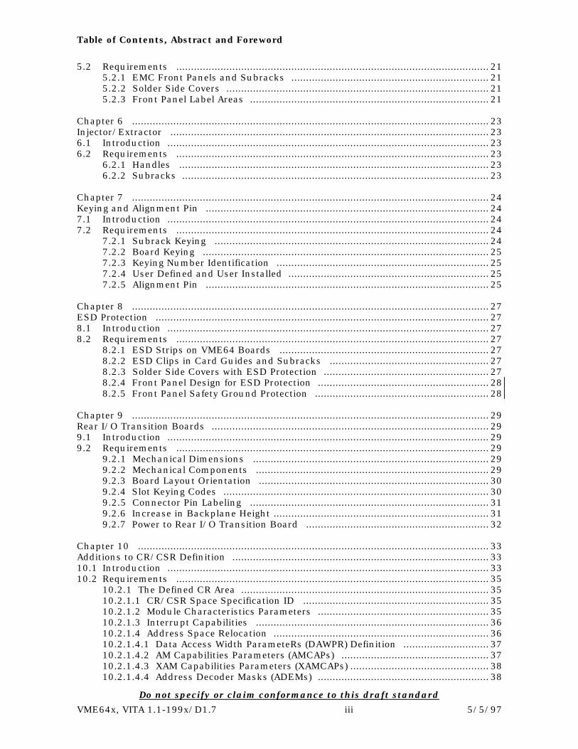
Table of Contents, Abstract and Foreword
Do not specify or claim conformance to this draft standard
VME64x, VITA 1.1-199x/D1.7 iii 5/5/97
5.2 Requirements .......................................................................................................... 215.2.1 EMC Front Panels and Subracks ................................................................... 215.2.2 Solder Side Covers ......................................................................................... 215.2.3 Front Panel Label Areas ................................................................................. 21
Chapter 6 ......................................................................................................................... 23Injector/Extractor ............................................................................................................ 236.1 Introduction ............................................................................................................. 236.2 Requirements .......................................................................................................... 23
6.2.1 Handles ......................................................................................................... 236.2.2 Subracks ........................................................................................................ 23
Chapter 7 ......................................................................................................................... 24Keying and Alignment Pin ................................................................................................ 247.1 Introduction ............................................................................................................. 247.2 Requirements .......................................................................................................... 24
7.2.1 Subrack Keying ............................................................................................. 247.2.2 Board Keying ................................................................................................. 257.2.3 Keying Number Identification ........................................................................ 257.2.4 User Defined and User Installed .................................................................... 257.2.5 Alignment Pin ................................................................................................ 25
Chapter 8 ......................................................................................................................... 27ESD Protection ................................................................................................................. 278.1 Introduction ............................................................................................................. 278.2 Requirements .......................................................................................................... 27
8.2.1 ESD Strips on VME64 Boards ....................................................................... 278.2.2 ESD Clips in Card Guides and Subracks ...................................................... 278.2.3 Solder Side Covers with ESD Protection ........................................................ 278.2.4 Front Panel Design for ESD Protection .......................................................... 288.2.5 Front Panel Safety Ground Protection ........................................................... 28
Chapter 9 ......................................................................................................................... 29Rear I/O Transition Boards .............................................................................................. 299.1 Introduction ............................................................................................................. 299.2 Requirements .......................................................................................................... 29
9.2.1 Mechanical Dimensions ................................................................................ 299.2.2 Mechanical Components ............................................................................... 299.2.3 Board Layout Orientation .............................................................................. 309.2.4 Slot Keying Codes .......................................................................................... 309.2.5 Connector Pin Labeling ................................................................................. 319.2.6 Increase in Backplane Height ......................................................................... 319.2.7 Power to Rear I/O Transition Board .............................................................. 32
Chapter 10 ....................................................................................................................... 33Additions to CR/CSR Definition ....................................................................................... 3310.1 Introduction ............................................................................................................. 3310.2 Requirements .......................................................................................................... 35
10.2.1 The Defined CR Area .................................................................................... 3510.2.1.1 CR/CSR Space Specification ID ............................................................... 3510.2.1.2 Module Characteristics Parameters .......................................................... 3510.2.1.3 Interrupt Capabilities ............................................................................... 3610.2.1.4 Address Space Relocation ......................................................................... 3610.2.1.4.1 Data Access Width ParameteRs (DAWPR) Definition ............................. 3710.2.1.4.2 AM Capabilities Parameters (AMCAPs) .................................................. 3710.2.1.4.3 XAM Capabilities Parameters (XAMCAPs) ............................................... 3810.2.1.4.4 Address Decoder Masks (ADEMs) .......................................................... 38

Table of Contents, Abstract and Foreword
Do not specify or claim conformance to this draft standard
VME64x, VITA 1.1-199x/D1.7 iv 5/5/97
10.2.1.5 Master Addressing Capabilities ................................................................ 4010.2.2 The Defined CSR Area .................................................................................. 4010.2.2.1 Additions to the Bit Set and Bit Clear Registers ........................................ 4010.2.2.2 Address Decoder compaRe (ADER) Registers ........................................... 4010.2.3 The User CR Area ........................................................................................ 4410.2.4 The Configuration RAM (CRAM) Area .......................................................... 4410.2.5 The User CSR Area ...................................................................................... 4610.2.6 Board Serial Number .................................................................................... 46
Chapter 11 ....................................................................................................................... 512eVME Protocol ................................................................................................................ 5111.1 Introduction ............................................................................................................. 51
11.1.1 2 Edge Handshakes ..................................................................................... 5111.1.2 Address Phases ............................................................................................ 5111.1.3 Remapping the LWORD* Line ...................................................................... 5111.1.4 Extended AM Codes ..................................................................................... 5111.1.5 Address Modes ............................................................................................ 5211.1.6 Known Length Block Transfers .................................................................... 5211.1.7 Slave Terminated Block Transfers ............................................................... 5211.1.8 Slave Suspended Transfers ......................................................................... 5311.1.9 Slave Error States ........................................................................................ 5311.1.10 Master Terminated Block Transfers ........................................................... 53
11.2 Requirements .......................................................................................................... 5311.2.1 Transceivers and Connectors ...................................................................... 5311.2.2 Extended AM Codes ..................................................................................... 5311.2.3 Data Size ...................................................................................................... 5411.2.4 Protocols, General ....................................................................................... 5411.2.5 Timing .......................................................................................................... 5511.2.6 Address Phase Protocol and Timing ............................................................. 5511.2.7 Data Phase Protocol and Timing .................................................................. 56
Appendix A ....................................................................................................................... 60Glossary of Additional VME64x Terms ............................................................................. 60
Appendix B ....................................................................................................................... 62Additional VME64x Signal/Pin Descriptions .................................................................... 62
Appendix C ....................................................................................................................... 64VME64 and VME64x Function Mnemonics ...................................................................... 64
Appendix D ....................................................................................................................... 67IEEE 1101.2-1992 Background ......................................................................................... 67
List of Figures
Figure 3-1 Backplane Termination Network using +3.3V Power ................................ 14Figure 4-1 P0 Connector Layout Position on VME64x Boards ..................................... 18Figure 4-2 J0 Connector Layout Position on VME64x Backplanes ............................ 19Figure 4-3 Backplane Left and Right End Dimensions ............................................... 20Figure 5-1 Front Panel Label Areas ............................................................................ 22Figure 5-2 Injector/Extractor Handle Label Area ....................................................... 22Figure 7-1 Keying Hole Positions and Associated Keying Codes ................................ 26Figure 9-1 Front and Rear Board Orientation & Connector Pin Labeling ................... 31Figure 10-1 Structure of CR/CSR Space ...................................................................... 34Figure 12-1 2eVME Address Broadcast ........................................................................ 69

Table of Contents, Abstract and Foreword
Do not specify or claim conformance to this draft standard
VME64x, VITA 1.1-199x/D1.7 v 5/5/97
Figure 12-2 2eVME Address Broadcast - Slave Suspend Response ............................. 70Figure 12-3 2eVME Address Broadcast - Slave Stop/Error Response .......................... 71Figure 12-4 2eVME Address Broadcast - Slave Suspend/Stop/Error Response .......... 72Figure 12-5 2eVME Read Data Transfers - Master Termination ................................... 73Figure 12-6 2eVME Read Data Transfers - Slave Suspend ........................................... 74Figure 12-7 2eVME Read Data Transfers - Slave Stop/Error on Odd Beat ................... 75Figure 12-8 2eVME Read Data Transfers - Slave Stop/Error on Even Beat ................. 76Figure 12-9 2eVME Write Data Transfers - Master Termination ................................... 77Figure 12-10 2eVME Write Data Transfers - Slave Suspend .......................................... 78Figure 12-11 2eVME Write Data Transfers - Slave Stop/Error on Odd Beat .................. 79Figure 12-12 2eVME Write Data Transfers - Slave Stop/Error on Even Beat ................. 80
List of Tables
Table 3-1 P1/J1 & P2/J2 Rows z & d Pin Assignments ...................................................7Table 3-2 Geographical Address Pin Assignments ...........................................................9Table 4-1 P0/J0/RJ0/RP0 Connector Pin Labeling .......................................................17Table 10-1 Slave Characteristics Parameter ...................................................................35Table 10-2 Master Characteristics Parameter ..................................................................36Table 10-3 Data Access Width Parameter (DAWPR) Definition ........................................37Table 10-4 Address Decoder Mask (ADEM) Definition .....................................................39Table 10-5 Address Relocation CR Examples ..................................................................40Table 10-6 Bit Set Register Assignment ...........................................................................41Table 10-7 Bit Clear Register Assignment .......................................................................41Table 10-8 Address Decoder compaRe (ADER) Registers .................................................42Table 10-9 Address Relocation CR/CSR Examples ..........................................................44Table 10-10 CRAM_ACCESS_WIDTH Definition ................................................................45Table 10-11 Serial Number Example .................................................................................47Table 10-12 Defined Configuration ROM Assignments ......................................................48Table 10-13 Defined Control/Status Register (CSR) Assignments ....................................50Table 11-1 Extended Address Modifier Line Definition ....................................................51Table 11-2 6U 2eVME Extended Address Modifier Codes ................................................52Table 11-3 3U 2eVME Extended Address Modifier Codes ................................................52Table 11-4 6U VME64x Signal Field Definition ................................................................57Table 11-5 3U VME64x Signal Field Definition ................................................................57Table 11-6 2eVME Specific Timing Parameters ...............................................................58Table 11-7 2eVME Timing Parameters .............................................................................58
AbstractThis standard is an extension of the VME64 Standard, VITA 1-1994. It defines a set offeatures that can be added to VME and VME64 boards, backplanes and subracks. Themajor new features defined in this draft standard are: 1) Expanded 160 pin P1/J1 &P2/J2 connectors, 2) an optional 95 pin 2 mm hard metric P0/J0 connector for more userdefined I/O, 3) +3.3V and 48V power plus more +5V power, 4) 35 more signal groundreturns, 5) 46 more user defined I/O pins on the P2/J2 connector, 6) 12 spare busedsignal pins plus 2 unbused pins on the P1/J1 connector for future growth, 7) pinassignments for a test and maintenance sub-bus interface, 8) slot geographicaladdressing, 9) mechanical support for EMC protection, 10) mechanical support for ESDprotection, 11) solder side covers, 12) injector/extractor handle with locking feature, 13)board keying to specific subrack slots, 14) multifunction alignment pin, 15) reserved frontpanel area for labels, 16) Rear I/O Transition Board definition, 17) added CR/CSRdefinition, 18) support for hot swap, and 19) 2 edge VME protocol.

Table of Contents, Abstract and Foreword
Do not specify or claim conformance to this draft standard
VME64x, VITA 1.1-199x/D1.7 vi 5/5/97
ForewordVME became the industrial bus of choice in the 80's with hundreds of manufacturerssupplying more than a thousand different boards to the world-wide market place.Thousands of customers utilized VME for a broad number of applications.
In the late 80's, the VME's draft standard was expanded for 64 bit data and addresscapability, which also doubled the throughput. Locks, Configuration ROM / Control &Status Registers (CR/CSR), rescinding DTACK*, auto system control detection, auto slotID, plus optional shielded DIN connectors were also added. These additional featureseffectively transformed VME from an 80's bus to a 90's bus, which allows VME to be usedin even more demanding applications for the early 90's. This standard is commonlyreferred to as VME64.
In the summer of 1993 the VITA Standards Organization (VSO) agreed to publish theVME64 Standard. It was also agreed to use additional standards to add features as theyare agreed upon by the VSO membership. This standard is a collection of additionalfeatures as agreed upon during 1994, 1995 and the first half of 1996. There will mostlikely be follow on standards with even more features.
Features added to VME64 in this draft standard encompass twenty major areas:
1) "z" and "d" pin rows to the P1/J1 and P2/J2 connectors for 160 pins in eachconnector.
2) An optional 2 mm hard metric 95 signal pin plus 19 or 38 ground pins P0/J0connector for more user defined I/O through the backplane.
3) Supply voltages of +3.3 and 48 volts, plus more +5V power
4) 35 more signal ground returns between VME64x boards and VME64x backplanes fora total of 47 signal ground returns.
5) 46 more user defined I/O pins on the P2/J2 connector pair.
6) 12 bused spare pins and associated bused lines in the backplane, plus 2 unbusedspare pins on the P1/J1 connector for future definition.
7) Pins allocated for a test and maintenance bus to be defined in another draftstandard.
8) Slot geographical addressing.
9) Mechanical support for electromagnetic compatibility (EMC) control.
10) Mechanical support for electrostatic discharge (ESD) control.
11) Solder side covers with ESD protection.
12) An injection/extraction handle with a locking feature.
13) User installed board to slot keying
14) Alignment pin which supports solid keying, improved connector alignment, frontpanel ESD protection and EMC gasket alignment.
15) Reserved area on the front panel for attachment of ID and/or bar code labels.
16) Rear I/O transition boards.
17) Added CR/CSR definition.
18) Supporting specifications for hot swap.
19) 2eVME: fast 2 edge protocol.
Some of these features are independent of one another. Others are tied close together,such as the usage of +3.3 V which requires the new 160 pin connector for the P1connector on VME64x boards and the usage of the VME64x backplane. If the 160 pinconnector is used on a VME64x board, the usage of 3.3 volt power, 48 volt power, hotswap control, serial bus, etc. are independent of one another.

Table of Contents, Abstract and Foreword
Do not specify or claim conformance to this draft standard
VME64x, VITA 1.1-199x/D1.7 vii 5/5/97
VME64 Extensions and VME64x Usage:The phrase "VME64 Extension" has been shortened to VME64x, where "x" implies the"Extensions" word. In product data sheets, user manuals, advertising and otherpromotional literature, it is encouraged that only these two phrases be used whenreferencing this draft standard.
Wayne FischerVME64x Chair & Draft Editor
The following people were on the canvas balloting committee:
>>> List to be provided. <<<
----- the following 8 sections will not be in the final standard -----
Comments , Correction and/or AdditionsAnyone wishing to provide comments, corrections and/or additions to this proposedstandard, please direct them to the task group chair:
Wayne Fischer, VME64x Chair & Draft EditorFORCE COMPUTERS Inc., A Solectron Subsidiary
2001 Logic Drive, San Jose, CA 95124Ph: 408-369-6250 Fx: 408-371-3992
Em: [email protected] Ws: http://www.forcecomputers.com
The best way to provide corrections and small additions is via marking up the specificpages and faxing them to the chair. For longer additions, the chair prefers to received justtextual information via e-mail. This draft standard is being prepared in Microsoft Word7.0, under Windows95.
VSO and Other StandardsShould anyone want information on other standards being developed by VSO, VMEProduct Directories, VME Handbooks, or general information on the VME market, pleasecontact the VITA office at the address, phone number or web site given on the front cover.Copies of the VSO minutes plus VSO meeting announcements and agenda can beretrieved from the VITA web site listed on the front cover.
Draft Copies on Web SitesCopies of this draft standard are available on FORCE's web site,http://www.forcecomputers.com (under the Standards & Technology Button), and onVITA's web site, http://www.vita.com (under the VSO Button) in Adobe Acrobat (.pdf) fileformat. It is best to use versions 3.0 of the Adobe Reader.
Change BarsAll paragraphs changed in this draft from draft 1.6 are marked with a change bar on theright side of the paragraph. Any table entry that was changed will have a double bar onthe right side of changed entry.

Table of Contents, Abstract and Foreword
Do not specify or claim conformance to this draft standard
VME64x, VITA 1.1-199x/D1.7 viii 5/5/97
Draft SummaryOriginal content of this draft standard was presented and agreed upon at the March 7 & 8,1994 VSO meeting. At the May 11 & 12, 1994 VSO meeting the standard name wasagreed upon. At the July 18 & 19, 1994 VSO meeting 48V power was added, plus theESD rules were refined. At the September 7 & 8, 1994 VSO meeting, basic agreement wasreached on the mechanical & electrical definition of the 160 pin connector, including 4pins for mate-first-break-last (MFBL). Agreement was also reached on the z & d rows ofboth the P1/J1 and P2/J2 connector pairs. The proposed P0/J0 connector became a userdefined connector area, with most of the proposed new signals moved to the P1/J1connector. At the November 16 & 17, 1994 VSO meeting, it was agreed to drop parityfrom the VME64 Extensions Draft Standard, plus clarify the P0/J0 connector area andextend the 48V operational range.
At the January 4 & 5, 1995 meeting is was agreed to add keying and reassign 8 pins onthe "d" row of the P1/J1 connector. No changes were made at the March 8 & 9, May 24 &25 and July 26 & 27, 1995 VSO meetings. At the September 20 & 21, 1995 VSO meetingit was agreed to allow the three VPC power pins to be used for additional +5V power andto define a reserved front panel area for ID and bar code labels. Assignment of theT&Mbus signal pins were done after the September VSO meeting.
At the November 14, 1995 High Availability VME64 Task Group meeting, basic agreementwas reach on the 2eMBLT protocol. At the January 17 & 18, 1996 VSO meeting it wasagreed to add an appendix on VME64x Compatibility, an appendix on VME64x Mnemonicsand a Rear I/O Transition Chapter. At the March 20 & 21, 1996 VSO meeting the 2eMBLTname was changed to 2eVME after Bob Downing observed that the real focus on the newprotocol was more on the two edge handshakes rather than the block transfer.
Between the November, 1995 and January, 1996 VSO meetings, the first task group ballotwas conducted (on draft 1.0). As a result of this ballot, several items were changed. Themain items added to draft 1.1 were: 1) Chapter 8, Rear I/O Transition Board, 2)reorganized the chapter sequence, such that the ETL chapter is just before the 2eVMEchapter, 3), added an appendix for mnemonic definitions, 4) added an appendix oncompliance, and 5) incorporated comments from the first task group ballot. Chapter 11,2eVME, was left blank for draft 1.1, due to the extra time needed to get agreement on themodified 2eVME protocol.
The following major changes were made for draft 1.2 (dated June 26, 1996): 1) a completeupdate of Chapter 9, Additional CR/CSRs, and 2) a complete update of Chapter 11,2eVME Protocol, 3), changed all "VME64 Ext." to "VME64x", and 4) changed all RULE"shall" words to all caps & bolded "SHALL" words. In draft 1.3, the following majorchanges were made: 1) added backplane end dimensions, and 2) changed all rule"SHALL" words back lower case & unbolded "shall" words. Only a few minor edits weremade in generation of draft 1.4.
A second Task Group Ballot was performed on Draft 1.4. As a result of the ballot, thefollowing things were changed in draft 1.5: 1) moved appendix D to chapter 2 (VME64xCompliance), 2) adding 1101.2 informative appendix, 3) complete re-write of the CR/CSRchapter, and 4) changing the RTRY1* line name to RESP*.
The ETL and 160 pin Simulation and Analysis was completed in January, 1997. At theJanuary 1997 VSO meeting it was voted to de-couple the ETL chapter from the 2eVMEchapter. The 2eVME protocol can be run with incident wave switching and non-incidentwave switching and with either ETL or TTL bus transceivers. An added in-line circuit isneeded to achieve incident wave switching when using ETL devices. Both the ETL and the2eVME chapters were updated accordingly in draft 1.6.
The third task group ballot was done on draft 1.6. At the March 1997 VSO meeting a TaskGroup Ballot Review Committee (TGBRC) meeting was held. It was decided to delete theETL chapter and the Appendix that summarized the Simulation and Analysis. There were
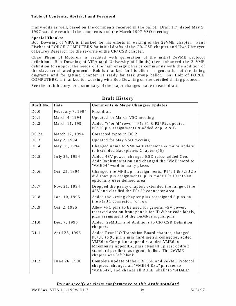
Table of Contents, Abstract and Foreword
Do not specify or claim conformance to this draft standard
VME64x, VITA 1.1-199x/D1.7 ix 5/5/97
many edits as well, based on the comments received in the ballot. Draft 1.7, dated May 5,1997 was the result of the comments and the March 1997 VSO meeting.
Special Thanks:Bob Downing of VIPA is thanked for his efforts in writing of the 2eVME chapter. PaulFischer of FORCE COMPUTERS for initial drafts of the CR/CSR chapter and Uwe Uhmeyerof LeCroy Research for the re-write of the CR/CSR chapter.
Chau Pham of Motorola is credited with generation of the initial 2eVME protocoldefinition. Bob Downing of VIPA (and University of Illinois) then enhanced the 2eVMEdefinition to support the needs of the high energy physics community with the addition ofthe slave terminated protocol. Bob is thanked for his efforts in generation of the timingdiagrams and for getting Chapter 11 ready for task group ballot. Kai Holz of FORCECOMPUTERS, is thanked for working with Bob Downing on the detailed timing protocol.
See the draft history for a summary of the major changes made to each draft.
Draft HistoryDraft No. Date Comments & Major Changes/Updates
D0.0 February 7, 1994 First draft
D0.1 March 4, 1994 Updated for March VSO meeting
D0.2 March 11, 1994 Added "z" & "d" rows in P1/P1 & P2/P2, updatedP0/J0 pin assignments & added App. A & B
D0.2a March 17, 1994 Corrected typos in D0.2
D0.3 May 2, 1994 Updated for May VSO meeting
D0.4 May 16, 1994 Changed name to VME64 Extensions & major updateto Extended Backplanes Chapter (#5)
D0.5 July 25, 1994 Added 48V power, changed ESD rules, added Geo.Addr Implementation and changed the "VME" word to"VME64" word in many places
D0.6 Oct. 25, 1994 Changed the MFBL pin assignments, P1/J1 & P2/J2 z& d rows pin assignments, plus made P0/J0 into anoptionally user defined area
D0.7 Nov. 21, 1994 Dropped the parity chapter, extended the range of the48V and clarified the P0/J0 connector area
D0.8 Jan. 10, 1995 Added the keying chapter plus reassigned 8 pins onthe P1/J1 connector, "d" row
D0.9 Oct. 2, 1995 Allow VPC pins to be used for general +5V power,reserved area on front panels for ID & bar code labels,plus assignment of the T&Mbus signal pins
D1.0 Dec. 7, 1995 Added 2eMBLT and Additions to CR/CSR Definitionchapters
D1.1 April 25, 1996 Added Rear I/O Transition Board chapter, changedP0/J0 to 95 pin 2 mm hard metric connector, addedVME64x Compliant appendix, added VME64xMnemonics appendix, plus cleaned up rest of draftstandard per first task group ballot. The 2eVMEchapter was left blank.
D1.2 June 26, 1996 Complete update of the CR/CSR and 2eVME Protocolchapters, changed all "VME64 Ext." phrases to"VME64x", and change all RULE "shall" to "SHALL".
Table of Contents, Abstract and Foreword
Do not specify or claim conformance to this draft standard
VME64x, VITA 1.1-199x/D1.7 x 5/5/97
D1.3 August 29, 1996 Added backplane end dimensions, and change allRULE "SHALL" words back to "shall" words.
D1.4 Sept. 20, 1996 A few minor edits
D1.5 Dec. 29, 1996 Many edits, plus 1) moved appendix D to chapter 2 ,2) added 1101.2 informative appendix, 3) re-write ofthe CR/CSR chapter, and 4) changed name of RTRY1*line to RESP*.
D1.6 Feb. 7, 1997 A few minor edits, de-coupled ETL from 2eVME, plusadded Simulation & Analysis Summary Appendix.
D1.7 May 5, 1997 Dropped the ETL chapter and Appendix E fromprevious draft, plus lots of edits as a result of 3rd taskgroup ballot and March '97 TGBRC meeting.
Issues & Concerns to be ResolvedFollowing are some of the issues and concerns that need to be resolved before finalapproval of this draft standard:
1) 2eVME skew timing numbers
Task Group BallotsMost of the edits in this draft are a direct result of the third task group ballot. After theMay 1997 VSO meeting, there will be a quick update of this draft standard, which will befollowed by the 4th task group ballot. It is hoped that this will be the last task groupballot before submittal to ANSI for the canvas ballot phase.

Chapters 1 through 11
Do not specify or claim conformance to this draft standard
VME64x, VITA 1.1-199x/D1.7 1 5/5/97
Chapter 1
Introduction to the VME64 Extensions Draft Standard
1.1 VME64 Extension Objectives
This draft standard documents features that can be added to VME64 boards, backplanesand subracks defined in the VME64 Standard.
The following new features are defined for optional usage in VME64x based applications:
• Addition of z & d rows to P1/J1 and P2/J2 connectors- With associated pin assignments
• A user defined 2 mm hard metric P0/J0 connector (area) between P1/J1 and P2/J2connectors- With 95 user defined signal pins and 19 or 38 ground pins
• 35 more signal ground return pins in the P1/J1 and P2/J2 connectors
• +3.3 volt power
• 48 volt power
• 3 more +5V power pins via the 3 VPC power pins
• Slot geographical addressing
• 12 reserved bused signal lines, plus 2 unbused pins for future expansion
• 46 more user defined pins on the P2/J2 connector
• Pins allocated for a test and maintenance bus (T&Mbus)
• 3 mate first-break-last precharge voltage pins for hot swap applications- 2 pins are on the P1/J1 connector and 1 pin on the P2/J2 connector- Can also be used for +5V power when board is locked into position- Required for hot swap applications
• 3 mate first-break-last precharge ground pins for hot swap applications- 2 pins are on the P1/J1 connector and 1 pin on the P2/J2 connector- Required for hot swap applications
• 2 reserved pins for individual slot power control for hot swap applications
• Two bused serial bus lines for hot swap control
• Front panel EMC protection
• ESD protection
• Solder side covers for hot swap and ESD protection
• Injector/Extractor handles with optional locking feature
• Board slot keying
• Multifunction alignment pin
• Reserved area on front panel for ID and bar code labels
• Rear I/O transition boards
• Added CR/CSR definition
• A 2eVME protocol that doubles the theoretical peak data transfer rate to 160 MB/sec

Chapters 1 through 11
Do not specify or claim conformance to this draft standard
VME64x, VITA 1.1-199x/D1.7 2 5/5/97
1.1.1 9U Boards, Backplanes and Subracks
9U VME, VME64 and VME64x boards, backplanes and subracks will not be referenced inthis draft standard. Another VSO standard is being developed that specifically definesthis capability.
1.2 Terminology
See Appendix A for the new terminology specific to the added features described in thisstandard. Terminology described in the VME64 Standard is not repeated in Appendix A.
1.3 References
The following publications are used in conjunction with this draft standard. When theyare superseded by an approved revision, that revision shall apply.
ANSI/VITA 1-1994 VME64 Standard, Approved April 10, 1995
IEC 603-xx 2.54 mm 160 pin connectors complementary to IEC 603-2 Style Cconnectors
IEC 1076-4-101 2 mm Hard Metric Connector
IEEE 1101.2-1992 IEEE Standard for Mechanical Core Specifications for Conduction-Cooled Eurocards
IEEE 1101.10-1996 IEEE Standard for additional Mechanical Specification forMicrocomputers using the IEEE 1101.1 Equipment Practice
IEEE P1101.11 IEEE Standard for Rear Plug-In Units for Microcomputers using theIEEE 1101.1 Equipment Practice, and the IEEE P1101.10 additionalMechanical Specifications, Draft 1.0, July 23, 1996
IEEE 1149.5-1995 IEEE Standard Module Test and Maintenance Bus
VITA 2-199x Enhanced Transceiver Logic Device Standard, Draft 0.4a,April 2, 1993
VITA 1.2-199x High Availability VME64 Draft Standard, Draft 0.2, November 9, 1995
VITA X-199x IEC 603-2 Connector Keys for Board-to-Backplane Slot Keying, (nodraft is available)
1.3.1 Connector Notes
The 160 pin connector defined in the IEC 603-xx connector specification is an expanded96 pin connector that is complementary to the IEC 603-2 Style C connector. Rows a, b & care identical in form, fit and function to the 96 pin IEC 603-2 Style C connectors, used inoriginal VME and VME64 applications. Rows z and d adds 64 pins to the outer shell for atotal of 160 pins.
The 160 pin connectors are forward and backward compatible to the 96 pin connectors.Boards with 160 pin connectors will plug into backplanes using 96 pin connectors andboards with 96 pin connectors will plug into backplanes using 160 pin connectors.
The IEC 1076-4-101 defines a family of 2 mm Hard Metric (HM) connectors. TheP0/J0/RJ0/RP0 connectors defined in Chapter 3 use a Type B 25 position 2 mmconnector variant with 19 positions. Each position provides 5 signal pins plus one or twoground pins.

Chapters 1 through 11
Do not specify or claim conformance to this draft standard
VME64x, VITA 1.1-199x/D1.7 3 5/5/97
1.4 Standard Terminology
To avoid confusion and to make very clear what the requirements for compliance are,many of the paragraphs in this standard are labeled with keywords that indicate the typeof information they contain. The keywords are listed below:
RuleRecommendationSuggestionPermissionObservation
Any text not labeled with one of these keywords describes the VME64 structure oroperation. It is written in either a descriptive or a narrative style. These keywords areused as follows:
Rule <chapter>.<number>:Rules form the basic framework of this draft standard. They are sometimes expressedin text form and sometimes in the form of figures, tables or drawings. All rules shallbe followed to ensure compatibility between board and backplane designs. All rulesuse the "shall" or "shall not" words to emphasize the importance of the rule. The"shall" or "shall not" words are reserved exclusively for stating rules in this draftstandard and are not used for any other purpose.
Recommendation <chapter>.<number>:Wherever a recommendation appears, designers would be wise to take the advicegiven. Doing otherwise might result in some awkward problems or poor performance.While the VME64x architecture has been designed to support high-performancesystems, it is possible to design a system that complies with all the rules but hasabysmal performance. In many cases a designer needs a certain level of experience inorder to design boards that deliver top performance. Recommendations found in thisstandard are based on this kind of experience and are provided to designers to speedtheir traversal of the learning curve.
Suggestion <chapter>.<number>:A suggestion contains advice which is helpful but not vital. The reader is encouragedto consider the advice before discarding it. Some design decisions that need to bemade in designing boards are difficult until experience has been gained. Suggestionsare included to help a designer who has not yet gained this experience. Somesuggestions have to do with designing boards that can be easily reconfigured forcompatibility with other boards, or with designing the board to make the job of systemdebugging easier.
Permission <chapter>.<number>:In some cases a rule does not specifically prohibit a certain design approach, but thereader might be left wondering whether that approach might violate the spirit of therule or whether it might lead to some subtle problem. Permissions reassure the readerthat a certain approach is acceptable and will cause no problems. The lower-caseword "may" is reserved exclusively for stating permissions in this draft standard and isnot used for any other purpose.
Observation <chapter>.<number>:Observations do not offer any specific advice. They usually follow naturally from whathas just been discussed. They spell out the implications of certain rules and bringattention to things that might otherwise be overlooked. They also give the rationalebehind certain rules so that the reader understands why the rule must be followed.

Chapters 1 through 11
Do not specify or claim conformance to this draft standard
VME64x, VITA 1.1-199x/D1.7 4 5/5/97
Chapter 2
VME64x Compliance
2.1 Introduction
In order for VME64x boards and VME64x backplanes to be labeled as VME64x Compliant,they are to incorporate a minimum set of functional features. This chapter specifies thatminimum set of features for 3U and 6U boards and backplanes.
Each of these features are described and documented in subsequent chapters within thisdraft standard.
2.2 Requirements
2.2.1 6U VME64x Board's Minimum Features
Rule 2.1:In order to be labeled as a VME64x compliant board, the 6U board shall incorporatethe following minimum functional features:
• Use the IEC 603-xx 160 pin connectors for both the P1 and P2 connectors
• Connect all assigned connector ground pins in rows z, a, b, and c to the board'sground plane (row d ground pins are optional)
Observation 2.1:All the other features defined in this draft standard are optional.
2.2.2 3U VME64x Board's Minimum Features
Rule 2.2:In order to be labeled as a VME64x compliant board, the 3U board shall incorporatethe following minimum functional features:
• Use the IEC 603-xx 160 pin connector for the P1 connector
• Connect all assigned connector ground pins in rows z, a, b, and c to the board'sground plane
Observation 2.2:All the other features defined in this draft standard are optional.
2.2.3 6U VME64x Backplane's Minimum Features
Rule 2.3:In order to be labeled as a VME64x compliant backplane, the 6U backplane shallincorporate the following minimum functional features:
• Monolithic PCB
• Use the IEC 603-xx 160 pin connectors for both the J1 and J2 connectors
• Connect all assigned connector ground pins in all rows to the backplane's groundplane
• Connect the geographical address pins as defined in this draft standard
• Route and terminate all defined VME64 and VME64x bused signal lines
• Provide power connection and distribution for +5V, +3.3V, +12V, -12V, +V1, +V2,-V1 and -V2.
Observation 2.3:All the other features defined in this draft standard are optional.

Chapters 1 through 11
Do not specify or claim conformance to this draft standard
VME64x, VITA 1.1-199x/D1.7 5 5/5/97
2.2.4 3U VME64x Backplane's Minimum Features
Rule 2.4:In order to be labeled as a VME64x compliant backplane, the 3U backplane shallincorporate the following minimum functional features:
• Use the IEC 603-2 160 pin connector for the J1 connector
• Connect all assigned connector ground pins in all rows to the backplane's groundplane
• Connect the geographical address pins as defined in this draft standard
• Route and terminate all defined VME64 and VME64x bused signal lines
• Provide power connection and distribution for +5V, +3.3V, +12V, -12V, +V1, +V2, -V1 and -V2.
Observation 2.4:All the other features defined in this draft standard are optional.
Chapters 1 through 11
Do not specify or claim conformance to this draft standard
VME64x, VITA 1.1-199x/D1.7 6 5/5/97
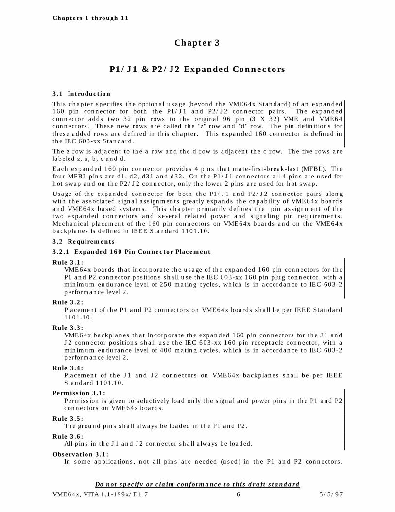
Chapter 3
P1/J1 & P2/J2 Expanded Connectors
3.1 Introduction
This chapter specifies the optional usage (beyond the VME64x Standard) of an expanded160 pin connector for both the P1/J1 and P2/J2 connector pairs. The expandedconnector adds two 32 pin rows to the original 96 pin (3 X 32) VME and VME64connectors. These new rows are called the "z" row and "d" row. The pin definitions forthese added rows are defined in this chapter. This expanded 160 connector is defined inthe IEC 603-xx Standard.
The z row is adjacent to the a row and the d row is adjacent the c row. The five rows arelabeled z, a, b, c and d.
Each expanded 160 pin connector provides 4 pins that mate-first-break-last (MFBL). Thefour MFBL pins are d1, d2, d31 and d32. On the P1/J1 connectors all 4 pins are used forhot swap and on the P2/J2 connector, only the lower 2 pins are used for hot swap.
Usage of the expanded connector for both the P1/J1 and P2/J2 connector pairs alongwith the associated signal assignments greatly expands the capability of VME64x boardsand VME64x based systems. This chapter primarily defines the pin assignment of thetwo expanded connectors and several related power and signaling pin requirements.Mechanical placement of the 160 pin connectors on VME64x boards and on the VME64xbackplanes is defined in IEEE Standard 1101.10.
3.2 Requirements
3.2.1 Expanded 160 Pin Connector Placement
Rule 3.1:VME64x boards that incorporate the usage of the expanded 160 pin connectors for theP1 and P2 connector positions shall use the IEC 603-xx 160 pin plug connector, with aminimum endurance level of 250 mating cycles, which is in accordance to IEC 603-2performance level 2.
Rule 3.2:Placement of the P1 and P2 connectors on VME64x boards shall be per IEEE Standard1101.10.
Rule 3.3:VME64x backplanes that incorporate the expanded 160 pin connectors for the J1 andJ2 connector positions shall use the IEC 603-xx 160 pin receptacle connector, with aminimum endurance level of 400 mating cycles, which is in accordance to IEC 603-2performance level 2.
Rule 3.4:Placement of the J1 and J2 connectors on VME64x backplanes shall be per IEEEStandard 1101.10.
Permission 3.1:Permission is given to selectively load only the signal and power pins in the P1 and P2connectors on VME64x boards.
Rule 3.5:The ground pins shall always be loaded in the P1 and P2.
Rule 3.6:All pins in the J1 and J2 connector shall always be loaded.
Observation 3.1:In some applications, not all pins are needed (used) in the P1 and P2 connectors.

Chapters 1 through 11
Do not specify or claim conformance to this draft standard
VME64x, VITA 1.1-199x/D1.7 7 5/5/97
Using selectively loaded connectors may provide a cost savings and will reduceinsertion/withdrawal forces.
3.2.2 P1/J1& P2/J2 Connectors, Rows z & d Pin Assignments
Rule 3.7:The signal pin assignment of the P1/J1 and P2/J2 connector pairs, rows z and d shallbe as defined in Table 3-1, P1/J1 and P2/J2 Rows z & d Pin Assignments. SeeAppendix B for definition of these signals.
Table 3-1 P1/J1 and P2/J2 Rows z & d Pin Assignments
Position P1/ J1 P2/ J2
No. Row z Row d Row z Row d
1 MPR VPC (1) UD UD (1)
2 GND GND (1) GND UD (1)
3 MCLK +V1 UD UD
4 GND +V2 GND UD
5 MSD RsvU UD UD
6 GND -V1 GND UD
7 MMD -V2 UD UD
8 GND RsvU GND UD
9 MCTL GAP* UD UD
10 GND GA0* GND UD
11 RESP* GA1* UD UD
12 GND +3.3V GND UD
13 RsvBus GA2* UD UD
14 GND +3.3V GND UD
15 RsvBus GA3* UD UD
16 GND +3.3V GND UD
17 RsvBus GA4* UD UD
18 GND +3.3V GND UD
19 RsvBus RsvBus UD UD
20 GND +3.3V GND UD
21 RsvBus RsvBus UD UD
22 GND +3.3V GND UD
23 RsvBus RsvBus UD UD
24 GND +3.3V GND UD
25 RsvBus RsvBus UD UD
26 GND +3.3V GND UD
27 RsvBus LI/I* UD UD
28 GND +3.3V GND UD
29 SBB LI/O* UD UD
30 GND +3.3V GND UD
31 SBA GND (1) UD GND (1)
32 GND VPC (1) GND VPC (1)
Chapters 1 through 11
Do not specify or claim conformance to this draft standard
VME64x, VITA 1.1-199x/D1.7 8 5/5/97
Note: (1) These pins are MFBL (mate-first-break-last) pins
Observation 3.2:Pins d1 and d2 of the P2 connector will mate before the other pins in rows z, a, b, cand d. Be aware that this may cause problems with user defined I/O signals whenusing these pins during hot swap operations.
Observation 3.3:Be aware that during hot swap operations, the VPC power may be applied first,therefore boards should be designed to tolerate the application of VPC before GND isconnected. The same applies during hot swap removal, VPC may be the last contact tobe removed.
Observation 3.4:Specification of the +3.3V, +V (+V1 & +V2) & -V (-V1 & -V2) [48V] and VPC power aredefined in Sections 2.2.4, 2.2.5 and 2.2.6 of this standard.
Rule 3.8:The GND pins shall be connected to the VME64x board's signal ground plane and theVME64x backplane's signal ground plane.
Rule 3.9:The UD, User Defined, pins shall be treated in the same fashion and have the samerules as the User Defined pins in the VME64 Standard.
Rule 3.10:The RsvBus (reserved bused) pins shall not be used by VME64x boards and arereserved for future use.
Rule 3.11:The 12 RsvBus pins, the 2 serial bus pin (SBA and SBB), the 5 test and maintenancebus (MPR, MCLK, MSD, MMD & MCTL) pins and the RESP* pin shall be bused andterminated on VME64x backplanes that implement a 160 pin connector for J1 in thesame fashion and have the same rules as the other VME64 bused signals defined inthe VME64 Standard.
Rule 3.12:The LI/I* (Live Insertion/Input) and LI/O* (Live Insertion/Output) pins shall bereserved for specification by the High Availability VME64 Draft Standard.
Observation 3.5:The LI/I*, LI/O* and RsvU pins are not bused but just feed through the backplane.
Rule 3.13:The two serial bus pins, SBA and SBB, shall be reserved for specification by the HighAvailability VME64 Draft Standard.
Rule 3.14:The five test and maintenance bus signal lines (MPR, MCLK, MSD, MMD & MCTL)shall be reserved for specification by the IEEE 1149.5 MTM-Bus Standard, withtailoring and additional commands specified in the High Availability VME64 DraftStandard.
Rule 3.15:The ground (GND) return path on the backplane shall present a maximum peak topeak voltage differential of 50 mV across the backplane, measured between anyconnector pin making contact with the GND rail, under conditions of maximumcurrent demand and all conditions of loading and noise expected for that system.Backplane termination networks are included in this rule. This applies for allfrequencies, including DC.
Rule 3.16:A voltage differential no greater than 50 mV shall be presented across all the powerrails (+5V, +3.3V, +V, -V, +12V and -12V) when measured between any two connectorpin making contact with the respective power rail, under conditions of maximum
Chapters 1 through 11
Do not specify or claim conformance to this draft standard
VME64x, VITA 1.1-199x/D1.7 9 5/5/97
current demand and all conditions of loading and noise expected for that system. Thisapplies for all frequencies, including DC.
Observation 3.6:While VME64x boards (with 160 pin connectors) can physically be plugged into aVME64 backplane (with 96 pin connectors), the two outer rows of pins, z and d, willnot be connected to anything.
Observation 3.7:Given Observation 3.xx, the user should determine from the vendor whether a specificVME64x compatible boards can be configured to operate correctly in a VME64backplane.
Permission 3.2:Vendors may design VME64x boards that can only be used in VME64x backplanes.
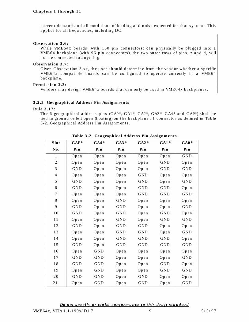
3.2.3 Geographical Address Pin Assignments
Rule 3.17:The 6 geographical address pins (GA0*, GA1*, GA2*, GA3*, GA4* and GAP*) shall betied to ground or left open (floating) on the backplane J1 connector as defined in Table3-2, Geographical Address Pin Assignments.
Table 3-2 Geographical Address Pin Assignments
Slot GAP* GA4* GA3* GA2* GA1* GA0*
No. Pin Pin Pin Pin Pin Pin
1 Open Open Open Open Open GND
2 Open Open Open Open GND Open
3 GND Open Open Open GND GND
4 Open Open Open GND Open Open
5 GND Open Open GND Open GND
6 GND Open Open GND GND Open
7 Open Open Open GND GND GND
8 Open Open GND Open Open Open
9 GND Open GND Open Open GND
10 GND Open GND Open GND Open
11 Open Open GND Open GND GND
12 GND Open GND GND Open Open
13 Open Open GND GND Open GND
14 Open Open GND GND GND Open
15 GND Open GND GND GND GND
16 Open GND Open Open Open Open
17 GND GND Open Open Open GND
18 GND GND Open Open GND Open
19 Open GND Open Open GND GND
20 GND GND Open GND Open Open
21. Open GND Open GND Open GND
Chapters 1 through 11
Do not specify or claim conformance to this draft standard
VME64x, VITA 1.1-199x/D1.7 10 5/5/97
Observation 3.8:Boards which use the geographical address signals will most likely use a pull upresistor to Vcc. The device that samples the levels of the geographical address pinswill read the inverted value of the slot number into which the board is plugged. Whenthe board is plugged into a VME/VME64 backplane the slot number will be zero with aparity error (GAP* open).
Rule 3.18:The board shall limit the current through each geographical address pin to amaximum of 2 mA.
3.2.4 +3.3V Power
Rule 3.19:The +3.3V power supplied to each slot on the VME64x backplane shall remain withinthe limits of +3.25V to +3.45V, including regulation variation, noise and ripplefrequencies to 20 MHz.
Rule 3.20:The current drawn for +3.3V pins shall follow the maximum current draw per powerpin as specified in the VME64 Standard, Figure 5-7, Current Rating For Power Pins.
Observation 3.9:If the maximum board ambient temperature is 60o C, the maximum current that canbe drawn per power pin in a multi-pin configuration is 1.25 Amp. With 10 +3.3Vpower pins on the P1/J1 connector pair, a nominal 41 watts of +3.3V power can besupplied to a VME64x board.
Rule 3.21:+3.3V, +5V, +12V, -12V and 48V power will ramp up and down independently of oneanother. Boards shall be designed to accommodate any combination of power up anddown sequence without causing board failure.
2.2.5 48V Power
Rule 3.22:The 48V power supplied to each slot via the +V (+V1 & +V2) and -V (-V1 & -V2) powerpins on the VME64x backplanes shall remain within the limits of 38V to 75V,including regulation variation, noise and ripple frequencies to 20 MHz.
Observation 3.10:A nominal voltage of either 48 V or 60 V may be used in VME64x boards and systemsfor telecom and military type applications.
Rule 3.23:The current drawn for the +V1, +V2, -V1 and -V2 pins shall follow the maximumcurrent draw per power pin specified in the VME64 Standard, Figure 5-7, CurrentRating For Power Pins.
Rule 3.24:Each board's power draw of the 48V power shall be balanced between the +V (+V1 plus+V2) and -V (-V1 plus -V2) power pins, with no more than 1 mA of current goingthrough the ground pins.
Recommendation 3.1:It is highly recommended that the 48V leakage current be kept below 100 uA.
Rule 3.25:The system power supply of the 48V power shall ensure that the +V (+V1 & +V2)voltage is always above or equal to the ground voltage level and that the -V (-V1 & -V2)voltage is always below or equal to the ground voltage level.
Observation 3.11:If the +V1 and +V2 voltage rails are tied to ground and the +12V power is used, the

Chapters 1 through 11
Do not specify or claim conformance to this draft standard
VME64x, VITA 1.1-199x/D1.7 11 5/5/97
nominal voltage between the +12V and the -V1 and -V2 power rails is 60 volts. Withvoltage tolerances, the 60 volt maximum is well exceeded.
Observation 3.12:System implementors and users should be aware that the United States UnderwritersLaboratory (UL) rules that whenever any two power points within a system (black box)exceeds 60 V, it is considered unsafe for "human operation". The design of boards willallow for larger voltages between any combination of power rails. But, how a "VME64xSystem" is integrated is the responsibility of the system integrator, and should complywith all applicable laws and regulations with respect to safety and other computerrequirements, including EMC.
Observation 3.13:For some applications, dual 48 V power rails are required. It may be necessary tobuild backplanes that split the +V1 and +V2 into two power rails, and/or split the -V1and-V2 into two power rails.
Recommendation 3.2: The usage of single or dual 48V supply and the decision whether the negative or thepositive poles will be tied together, is up to the system configuration. Therefore it isrecommended that generic VME64x backplanes provide individual connections foreach of the +V1, +V2, -V1, -V2 power rails.
Recommendation 3.3:Boards that are designed to support the dual 48 V power rails should place diodes orequivalent on each of +V (+V1 and +V2) power pins and/or on each of the -V (-V1 and -V2) power pins. In event one of the power rails fails, the other power rail will supplythe main power to the board.
3.2.6 VPC Power and Additional +5V Power
VPC is the three pre-charge voltage pins on the P1/J1 and P2/J2 connectors. These threepins mate a minimum of 1.5 mm before the other pins during live insertion. During livewithdraw, these pins are the last to break contact. This feature is required to support thehot swap capability defined in the High Availability VME64 (H.A.VME) Draft Standard.
Rule 3.26:If VPC power is used, all three VPC power pins shall be used on 6U boards and bothVPC power pins on 3U boards shall be used.
Rule 3.27:The VPC voltage pins shall be connected directly to the backplane +5V power plane.
Rule 3.28:Boards shall limit the peak current drawn through each VPC power pin to 100 mAduring hot swap operations.
Permission 3.3:VPC power pins may be used for additional +5V power during non hot swapoperations.
Rule 3.29:If the VPC power pins are used for additional +5V power, the current drawn shallfollow the maximum current draw per power pin as specified in the VME64 Standard,Figure 5-7, Current Rating For Power Pins.
Observation 3.14:If VPC power is shorted to +5V power on a board, the board can't be used in hot swapapplications.

Chapters 1 through 11
Do not specify or claim conformance to this draft standard
VME64x, VITA 1.1-199x/D1.7 12 5/5/97
3.2.7 Reset and ACFail
Rule 3.30:If +3.3V and/or 48V power is used to power boards plugged into the backplane, theSYSRESET* and ACFAIL* signals operations levels shall include the proper functionallevels of +3.3V and 48V.
Observation 3.15:Rule 3.28 implies that the SYSRESET* and ACFAIL* signal lines can not be releasedhigh (normal operation) until the monitored power voltages are in the proper operationlevels. When any of the power signals goes outside the proper operation range, theSYSRESET* signal line is asserted. The timing of these two signals remains the sameas defined in the VME64 Standard.
3.2.8 Board Power Dissipation
Recommendation 3.4:It is recommended that board suppliers specify a board's maximum power dissipationand identify "hot spots" and any thermally sensitive components, which require highercooling airflow than normal.
3.2.9 Backplane Termination Network using +3.3V Supply
Permission 3.4:Permission is given to use the +3.3V supply voltage for the backplane terminationnetworks.
Rule 3.31:If the +3.3V supply voltage is used for the backplane termination network, the networkshall be in compliance with the network shown in Figure 3-1 Backplane TerminationNetwork using +3.3V Power.
Recommendation 3.5:For VME64x backplanes that use +3.3V power for the termination network, it is highlyrecommended that a large warning label be part of the back side of the backplanestating that the termination network is supplied by the +3.3V power rails. +3.3Vpower is required for proper VME64x system operation.
3.2.10 Monolithic Backplanes
Rule 3.32:6U VME64x backplanes shall be constructed as a single (monolithic) printed circuitboard.
Observation 3.16:The main reason for Rule 3.30 is to provide solid voltage and ground planes on thebackplane to minimize the noise and voltage differentials between VME64x boards andVME64x backplanes.
3.2.11 Geographical Address Implementation
This section ties together the implementation of geographical addressing and CR/CSRs ifboth are implemented on a VME64x board.
Geographical addressing as defined in section 2.2.3 is to be used by VME64x boards toautomatically identify into which VME64x backplane slot it is plugged. Based on thatinformation, software can automatically configure the boards for slot specific functionality.Initialization and configuration of the CR/CSRs is an extension of the capability.
The monarch is generally the first CPU board to gain access to the backplane and systemright after power up to configure the system. The monarch may also be the CPU boardwhich controls and manages the main system operation during normal operations.

Chapters 1 through 11
Do not specify or claim conformance to this draft standard
VME64x, VITA 1.1-199x/D1.7 13 5/5/97
Rule 3.33:If a board implements both geographical addressing and CR/CSR capability, the BARvalue shall be derived from the geographical address pins.
Observation 3.17:The above rule will automatically place each board's CR/CSR address in the properA24 address space. This will allow the system's monarch to search the CR/CSRaddress space and quickly determine which VME64x boards are plugged into thebackplane and then configure the board.
Recommendation 3.6:It is recommended that boards implementing Rule 3.31 parity check the geographicaladdress. If bad parity is found, the local address should be set to decimal 30 (Ox1E)(the amnesia address).
Permission 3.5:Permission is given not to check geographical address parity.
Permission 3.6:Permission is given not to respond if bad geographical address parity is detected.
Rule 3.34:Monarchs that search the CR/CSRs space for presence of VME64x boards shall alsolook for boards at amnesia address 30 (Ox1E) and take the appropriate action if one isfound at that address.
Suggestion 3.1:VME64x boards that need to be backward compatible to original VME backplanes, mayadd some sense circuitry and 5 switches or 5 jumpers or some programmable logic.When the board senses that none of the GA*[4..0] lines are tied to ground (board notplugged into a VME64x backplane), it will use the state of the 5 switches or 5 jumpersor programmable logic values for the geographical address value.
Observation 3.18:It is up to the system designer to determine how to handle multiple occurrence ofgeographical parity errors, should it happen.
Observation 3.19:The BAR bits 7 to 3 defined in the CR/CSR regions, correspond to A[23..19] in theCR/CSR space. See Table 2-31 and section 2.3.12 in the VME64 Standard for moreexplanation.
3.2.12 J2 Connector Tail Lengths
Recommendation 3.7:The generic J2 connector pin tail lengths should be 17 mm on all pins except, b3through b11, b14 through b 21 and b23 through b30. The short pin tail length shouldbe 5.0 mm or less.
Observation 3.20:Recommendation 3.8 enforces protection of the electrical properties of the busedsignals connected to the b row of the P2/J2 connectors. The tail length defined for thepower and ground connection and the user defined pins guarantees compatibility toChapter 9 of this draft standard.

Chapters 1 through 11
Do not specify or claim conformance to this draft standard
VME64x, VITA 1.1-199x/D1.7 14 5/5/97
Resistor Networks that Provides the Required Termination using +3.3V Power
Thevenin Equivalent for each Network using +3.3V Power
Signal Line
220 ohms +/- 5%
220 ohms +/- 5%
1.8K ohms +/- 5%
1.8K ohms +/- 5%
0.1 uf 0.1 uf
+3.3V +/- 5% +3.3V +/- 5%
R = 196 ohms +/- 5% V = 2.94 +/- 5%
Figure 3-1 Backplane Termination Network using +3.3V Power

Chapters 1 through 11
Do not specify or claim conformance to this draft standard
VME64x, VITA 1.1-199x/D1.7 15 5/5/97
Chapter 4
P0/J0 Connector Area andVME64x Backplane End Dimensions
4.1 Introduction
At times manufacturers and users of VME64x boards have a need for additional andsometimes specialized I/O through the backplane. This chapter specifies therequirements and provides observations for implementation of user defined I/O betweenthe P1/J1 and P2/J2 connectors.
This area is commonly called the P0/J0 connector area, even though four connectors areinvolved: a connector on the front VME64x board (P0), a connector on the front of thebackplane (J0), a connector shroud on the rear of the backplane (RJ0) and a connector onthe rear plug in board (RP0) or the end of cable which plugs into the rear connector. Thismay also be written as: P0/J0/RJ0/RP0, where the "R" means rear. (The rear connectorshroud goes over the male tail pins and provides the necessary alignment and othermechanical support for normal connector mating.)
See Chapter 9 for the definition of rear I/O transition boards and for mechanicalalignment with the backplane. See Figure 9-1 for a pictorial of the connector placementson VME64x boards, VME64x backplanes and rear I/O transition boards.
When the J0 2 mm connector is mounted on VME64x backplanes, the backplane's leftand right end mechanical dimensions must be shifted left, to accommodate theconnector's added width and position. The last section of this chapter defines VME64xbackplane's left and right end dimension.
4.2 Requirements
Permission 4.1: Additional user defined I/O connector space may be obtained if the mechanicalmember between J1 and J2 connector pairs on VME backplanes, shown in Figure 7-18of the VME64 Standard, is removed.
Rule 4.1:Whenever a structural member is not used between the J1 and J2 connectors onVME64x backplanes, the VME64x backplane shall maintain sufficient rigidity to meetthe mechanical requirements specified in IEEE Standard 1101.1.
Observation 4.1:VME64x boards using I/O connectors between P1 and P2 may conflict withVME/VME64 backplanes that have a mechanical structure member between J1 andJ2 connectors.
4.2.1 Connector Selection
Rule 4.2: For generic user defined I/O between the P1/J1 and P2/J2 connectors, a 19 position,Type B, 2 mm hard metric, IEC 1076-4-101 connector shall be used. The connectorsshall be rated Performance Level 2 or better with a minimum of 250 insertionwithdrawal cycles.
Rule 4.3: For generic uses, the Type B, 2 mm hard metric IEC 1076-4-101 receptacle connectorshall be used on VME64x boards.

Chapters 1 through 11
Do not specify or claim conformance to this draft standard
VME64x, VITA 1.1-199x/D1.7 16 5/5/97
Rule 4.4: For generic uses, the Type B, 2 mm hard metric male IEC 1076-4-101 connector shallbe used on the VME64x backplanes. On the front side, rows z and f shall be length 3(11.2 mm) and rows a through e shall be length 1 (8.2 mm). On the rear side, the pintail lengths shall be 16 mm when straight through I/O is used, or 4.5 mm when a sub-bus is used.
Rule 4.5:When straight through I/O is used, a shroud over the rear tail pins shall be used thatmeets the mechanical offset dimensions defined in IEEE P1101.11.
Rule 4.6:Where the 2 mm hard metric IEC 1076-4-101 connector is used, the z and f row pinson the backplane's receptacle connector shall be connected to the backplane's groundplane as defined in Table 4-1, P0/J0 Connector Pin Labeling.
Rule 4.7:The z row shield on the plug connector can only be used if it does not protrudethrough the board's interboard separation plane.
Observation 4.2:The variant compatible of the 2 mm hard metric IEC 1076-4-101 connector familyprovides 95 contacts for user defined I/O. Additionally, two outer rows of contacts areconnected to ground on the backplane. When only the e row shield is used on theplug connector, 19 ground contacts are supplied to the board. The use of the e and zrow shields provide a total of 38 ground contacts.
4.2.2 Custom Connectors
Permission 4.2: Custom I/O connectors such as coaxial cable or fiber may also be used on VME64xboards and VME64x backplanes which require specialized custom I/O in the P0/J0connector area.
Observation 4.3:VME64x backplanes with custom I/O connectors will not be compatible with VME64xboards containing a P0 connector per Rule 4.2.
Recommendation 4.1:It is recommended that the keying scheme defined in this draft standard be used forboards and backplane slots that have custom I/O connectors.
Observation 4.4:For applications that are 1101.2 based, the VITA X-199x, IEC 603-2 Connector Key forBoard-to-Backplane Slot Keying should be used.
Rule 4.8:Any custom connector installed on the backplane in the J0 connector area shall allowthe plug in board’s rear edge to be installed (come to rest) within 12.5mm of thebackplane surface.
Observation 4.5:A connector with a height of greater than 12.5mm will protrude over the edge of theVME64x board into the board's component area when plugged into that slot. Thiswould prevent generic boards, that do not have a mating P0 connector, from beingplugged into that slot.
4.2.3 P0/J0 Connector Contact Labeling
Rule 4.9:The row and column labeling of the contacts in the P0/J0/RJ0/RP0 connector shall beas shown in Table 4-1, P0/J0/RJ0/RP0 Connector Contact Labeling.

Chapters 1 through 11
Do not specify or claim conformance to this draft standard
VME64x, VITA 1.1-199x/D1.7 17 5/5/97
Table 4-1 P0/J0/RJ0/RP0 Connector Contact Labeling
Pos. Row f Row e Row d Row c Rows b Row a Row z
1 GND UD UD UD UD UD GND
2 GND UD UD UD UD UD GND
3 GND UD UD UD UD UD GND
4 GND UD UD UD UD UD GND
5 GND UD UD UD UD UD GND
6 GND UD UD UD UD UD GND
7 GND UD UD UD UD UD GND
8 GND UD UD UD UD UD GND
9 GND UD UD UD UD UD GND
10 GND UD UD UD UD UD GND
11 GND UD UD UD UD UD GND
12 GND UD UD UD UD UD GND
13 GND UD UD UD UD UD GND
14 GND UD UD UD UD UD GND
15 GND UD UD UD UD UD GND
16 GND UD UD UD UD UD GND
17 GND UD UD UD UD UD GND
18 GND UD UD UD UD UD GND
19 GND UD UD UD UD UD GND
Observation 4.6:The J0/RJ0 connectors have seven physical rows of contacts, with the z and f contactrows connected to the backplane's ground plane. On the VME64x board, there is no zrow of contact holes Depending on the connector design, the P0 and RP0 connectorground contacts in the z and f row of the connector (which is on the connector shroud)will alternately connect to the board's f row of ground contacts.
Rule 4.10:The P0 and RP0 connector's z ground shield (on the solder side) can only be installed ifit does not protrude into the interboard separation plane defined in IEEE Standard1101.1.
Observation 4.7:Some of the 2 mm hard metric connector's z shields protrude into the interboardseparation plane, and therefore can not be used. When using the z shield on the P0and RP0 connectors, ensure that shield's component height does not violate theinterboard separation plane.
Observation 4.8:If only the f row of ground contacts are used in the P0 and RP0 connectors, then 19ground contacts are effectively provided. If both the f and z ground contacts are used,then 38 ground contacts are effectively provided.
Observation 4.9:Connector layout and position numbering method is the same as the P1/J1 and P2/J2connectors. Position 1 is near P1/J1's position 32 and position 19 is near P2/J2'sposition 1.

Chapters 1 through 11
Do not specify or claim conformance to this draft standard
VME64x, VITA 1.1-199x/D1.7 18 5/5/97
4.2.4 P0/J0 Connector Mounting
Rule 4.11: Mounting of the 19 position, 5+1 row, Type B, 2 mm hard metric IEC 1076-4-101 plugconnector on VME64x boards shall be as shown in Figure 4-1, when implemented
Rule 4.12: Mounting of the 19 position, 5+2 row, Type B, 2 mm hard metric IEC 1076-4-101receptacle connector on VME64x backplanes shall be as shown in Figure 4-2, whenimplemented.
4.2.5 Pin Current Ratings
Rule 4.13: The maximum current load per contact shall be in compliance to the IEC 1076-4-101.
Observation 4.10:When this draft standard was approved, the maximum current load per contact wasdefined to be 2.0 amp at 70o C when an alternate chess pattern of contacts are usedfor power. When adjacent contacts are grouped together for power, the maximumcurrent per contact is 1.0 amp at 70o C. The current rating of the shield contacts inrows z & f is 1.5 amp at the same temperature. For power ratings at othertemperatures, see IEC 1076-4-101.
Rule 4.14:The shield contacts are connected to logic ground on the backplane and boards. It isnot connected to frame ground. Although the shield contacts will provide a groundreturn path the current carrying capacity of the pins shall not be used in calculatingthe overall ground current carrying capacity.
<---- Edge of VME64x Board
1.26 +/- 0.05 mm
CL
Centered between P1 and P2 Connectors
P0 Connector ---->
P1 Connector ---->
d c b a z
f e d c b a
[1.50 mm ]
For holes dimensions, see connector specifications
Figure 4-1 P0 Connector Layout Position on VME64x Boards
(component side - top view)

Chapters 1 through 11
Do not specify or claim conformance to this draft standard
VME64x, VITA 1.1-199x/D1.7 19 5/5/97
1.85 +/- 0.05 mm
CL
Centered between J1 and J2 Connectors
J0 Connector---->
J1 Connector ---->
z a b c d
For holes dimensions, see connector specifications
z a b c d e f
Figure 4-2 J0 Connector Layout Position on VME64x Backplanes
(front view)
4.2.6 Backplane P0/J0 Keying
In some applications a slot board to backplane keying is required. In particular, IEEE1101.2 type applications does not use the front panel, but does require slot keying.
Recommendation 4.2: For applications that need a slot board to backplane keying capability, it isrecommended that the keys defined in VITA X-199x, IEC 603-2 Connector Keys forBoard-to-Backplane Slot Keying, be used.
4.2.7 VME64x Backplane End Dimensions
Mounting of the J0 2 mm connector on VME64x backplanes causes the backplane to beshifted to the left on both the left and right ends, over VME/VME64 backplanes. Only thetwo end dimensions are affected. All the other backplane dimensions remain the same asdefined in the VME64 Standard.
When two VME64x backplanes of less than 21 slots are mounted next to one another inthe same subrack, the gap between the two backplanes is designed to be 1 mm. In theVME64 Standard, this dimension is defined as 1.44 mm. Depending on the specificapplication needs, backplanes can be made wider. The incremental width should beconsistent such that when backplanes are mounted next to one another or mounted nextto other hardware, such as disk drive or power supplies, the gap always remains thesame, regardless of the backplane width and number of slots used.
Rule 4.15: The left and right end dimensions of minimum width VME64x backplanes shall be asshown in Figure 4-3.

Chapters 1 through 11
Do not specify or claim conformance to this draft standard
VME64x, VITA 1.1-199x/D1.7 20 5/5/97
Rule 4.16: Should VME64x backplanes need to be made wider, the incremental end dimensionsfor both left and right ends shall be in 5.08 mm (1 HP) increments.
Permission 4.2: For subrack air flow management purposes, the right end of 21 slot sized VME64xbackplanes can extend over the last interboard separation plane by 1.54 +0.00 -0.15mm.
Rule 4.17: Half shears shall not exceed 1.00 mm in height when used in VME64x applications.
Observation 4.11: Note that half shears are commonly used on side (end) plates of subracks to preventrotation and ensure accurate alignment of subrack horizontal members.
Observation 4.12:Some side (end) plates that utilize half shears for positioning of horizontal members,may not place half shears in the area of the backplane ends, as shown in Figure 4-3.
Observation 4.13:All the other backplane dimensions and tolerances remain the same as defined in theVME64 Standard.
First Interboard Separation
Plane
Last Interboard Separation
Plane
2.54 +0.00 -0.15
1.54 +0.00 -0.15
Left End Right End
Figure 4-3 Backplane Left and Right End Dimensions
(front view)
Observation 4.14:If the backplanes are mounted the other way, the backplanes may mechanicallyoverlap when being mounted to place consecutive connectors on 20.32 mm centers."
Chapters 1 through 11
Do not specify or claim conformance to this draft standard
VME64x, VITA 1.1-199x/D1.7 21 5/5/97
Chapter 5
EMC Front Panels and Subracks
5.1 Introduction
This chapter specifies the optional usage of EMC front panels on VME64x boards. Insome applications, there is a need to restrict the amount of EMI and RFI being radiatedfrom the front of VME64x subracks, without the aid of a special cover. The EMC frontpanels and subracks specified in IEEE Standard 1101.10, will provide this capability.
In some applications there is a need for attachment of identification and/or bar codelabels on the front panel. This chapter defines three recommended areas that VME64xboard suppliers may want to leave open for attachment of special labels.
Note that for VME64x boards and subracks being built according to IEEE 1101.2, IEEEStandard for Mechanical Core Specifications for Conduction-Cooled Eurocards, the EMCdesign defined in this chapter is not applicable.
5.2 Requirements
5.2.1 EMC Front Panels and Subracks
Rule 5.1:VME64x boards that require the use of an EMC front panel shall use the EMC frontpanel as specified in IEEE Standard 1101.10.
Rule 5.2:Should filler panels be used in conjunction with VME64x boards that have EMC frontpanels, the filler panels shall provide EMC protection. Filler panels shall comply withthe filler panels as specified in IEEE Standard 1101.10.
Rule 5.3:VME64x subracks that are to be used in conjunction with VME64x EMC front panelsshall meet the subrack specification given in IEEE Standard 1101.10.
Rule 5.4:The EMC front panels shall not be electrically connected to the board's logic groundplane nor the ESD strips (if implemented).
Rule 5.5:Whenever EMC front panels are implemented, the associated alignment pin on thefront panel and alignment hole in the subrack defined in IEEE 1101.10 shall also beused to keep boards properly positioned in the subrack.
5.2.2 Solder Side Covers
Recommendation 5.1:It is recommended that a cover as defined in IEEE Standard 1101.10 be used on thesolder side of VME64x board's PCB to prevent scraping of components and the stubs ofthrough hole components by the adjacent left slot's EMC contacts. (Thisrecommendation does not apply to IEEE 1101.2 based boards.)
5.2.3 Front Panel Label Areas
Recommendation 5.2:It is recommended that an area of 15 mm high by 20 mm wide be left open at thebottom of VME64x board's front panels for attachment of identification and/or barcode labels. See Figure 5-1, Front Panel Label Areas.
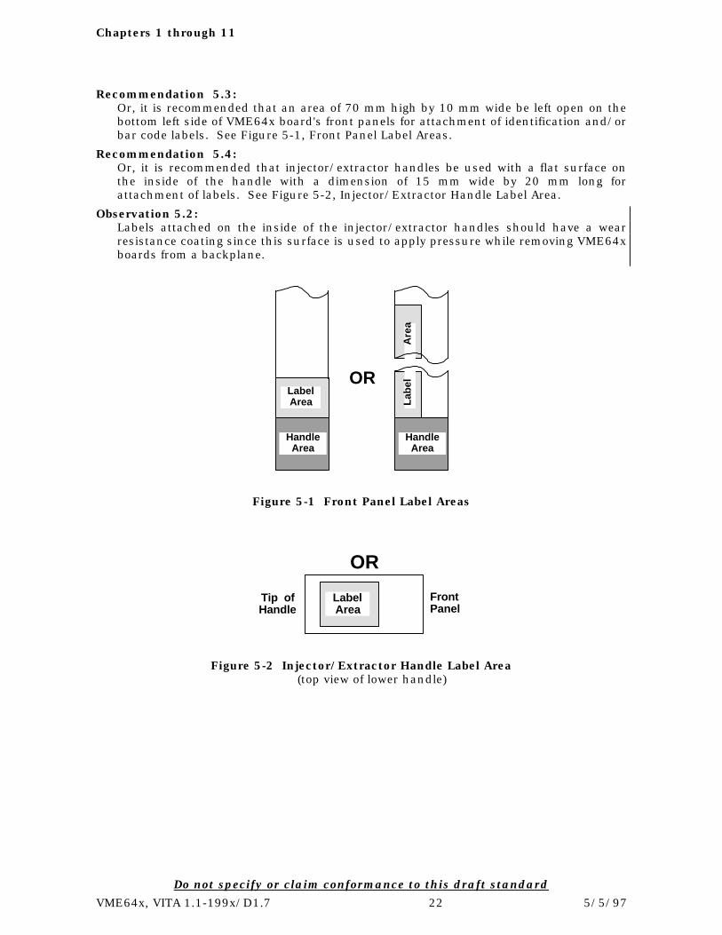
Chapters 1 through 11
Do not specify or claim conformance to this draft standard
VME64x, VITA 1.1-199x/D1.7 22 5/5/97
Recommendation 5.3:Or, it is recommended that an area of 70 mm high by 10 mm wide be left open on thebottom left side of VME64x board's front panels for attachment of identification and/orbar code labels. See Figure 5-1, Front Panel Label Areas.
Recommendation 5.4:Or, it is recommended that injector/extractor handles be used with a flat surface onthe inside of the handle with a dimension of 15 mm wide by 20 mm long forattachment of labels. See Figure 5-2, Injector/Extractor Handle Label Area.
Observation 5.2:Labels attached on the inside of the injector/extractor handles should have a wearresistance coating since this surface is used to apply pressure while removing VME64xboards from a backplane.
Handle Area
Label Area
Handle Area
Lab
el
A
rea
OR
Figure 5-1 Front Panel Label Areas
OR
Label Area
Front Panel
Tip of Handle
Figure 5-2 Injector/Extractor Handle Label Area(top view of lower handle)

Chapters 1 through 11
Do not specify or claim conformance to this draft standard
VME64x, VITA 1.1-199x/D1.7 23 5/5/97
Chapter 6
Injector/Extractor Handles
6.1 Introduction
In some applications, there may be a need for mechanical assistance during the insertionand/or removal (extraction) of VME64x boards into and out of VME64x subracks. Anoptional Injector/Extractor Handle and associated subrack defined in IEEE Standard1101.10 is ideal for this purpose.
The use of screws to secure VME64x boards to VME64x subrack is not allowed in someapplications. The screw heads can get damaged, plus the usage of a tool is required toremove and replace VME64x boards from a subrack. A self locking feature in the handlereplaces the need for front panel screws and will prevent VME64x boards from falling outunder harsh conditions, such as earthquakes, transportation and other high vibrationapplications.
Note that for VME64x boards and subracks being built according to IEEE 1101.2, theinjector/extractor handle design defined in this chapter is not applicable.
6.2 Requirements
6.2.1 Handles
Rule 6.1:Should an Injector/Extractor Handle be used on VME64x boards, it shall be incompliance with the handle defined in IEEE Standard 1101.10.
Recommendation 6.1:It is recommended that the Injector/Extractor Handle have a self locking feature,which would eliminate the optional use of front panel screws.
Observation 6.1:The Injector/Extractor Handle is backwards compatible to original VME handles,which allows boards using this handle to be plugged into original VME subracks.
Observation 6.2:For IEEE 1101.2 based applications, the handles defined in this chapter are notapplicable. The handles defined in IEEE 1101.2 are used.
6.2.2 Subracks
A special injector/extractor handle engagement comb is required on the front of VME64xsubracks that will support the use of the referenced Injector/Extractor Handle.
Rule 6.2:Should a VME64x subrack be used that supports the use of the Injector/ExtractorHandle, it shall be in compliance with the one defined in IEEE Standard 1101.10.
Observation 6.2:VME and VME64 boards are forward compatible and can be plugged in to the VME64xsubracks.
Chapters 1 through 11
Do not specify or claim conformance to this draft standard
VME64x, VITA 1.1-199x/D1.7 24 5/5/97
Chapter 7
Keying and Alignment Pin
7.1 Introduction
In many applications with I/O through the backplane's user defined pins, specific boardsare assigned to specific slots. Plugging the wrong board into a pre-defined slot may causethe system to operate improperly. Also, in some applications which assign some of theI/O pins to special power voltages, plugging a board into the wrong slot could havedisastrous results. This may include the destruction of the board being plugged in as wellas other boards in the same subrack. This becomes even more critical in hot swapapplications. Therefore there is the need for keying, where only keyed boards can beplugged into keyed subrack slots.
An optional keying mechanism for VME64x subracks and boards is defined in IEEEStandard 1101.10. This keying mechanism provides for three keying holes on the top andthree keying holes on the bottom of each board and each subrack slot. Each keying holecan be keyed with a "No Key" or a keying peg in one of four positions. This effectivelyprovides 5 key combinations per keying hole. With three keying holes on the top andthree on the bottom, this keying scheme provides a total of 5 x 5 x 5 x 5 x 5 x 5 = 15,625keying combinations.
A "No Key" hole in the subrack allows for a "family" of boards to be plugged into a specificslot. Boards with no keys installed can be plugged into any slot, as well as subrack slotswith no keys installed will allow for any board to be plugged into the subrack's slot.
The actual number of "hard" combinations, where all holes are keyed in both the boardand subrack slots is 4 x 4 x 4 x 4 x 4 x 4 = 4,096 combinations. In applications whereboth the top and bottom have identical keys, then 4 x 4 x 4 = 64 keying combinations arepossible.
An alignment pin and associated alignment hole is to be used as part of the keyingmechanism for better alignment during hot swap, for an ESD path from the front paneland for a solid keying blockage should the wrong board be inserted into a keyed slot.
Note that for VME64x boards and subracks being built according to IEEE 1101.2, IEEEStandard for Mechanical Core Specifications for Conduction-Cooled Eurocards, the keyingand alignment design defined in this chapter is not applicable.
7.2 Requirements
Observation 7.1:The features defined in this chapter are not applicable to IEEE 1101.2 basedapplications.
7.2.1 Subrack Keying
Rule 7.1:Should keying be provided in VME64x subracks, the keying mechanism defined inIEEE Standard 1101.10 for subracks shall be used.
Observation 7.2:Subrack keying hole positions and associated keying codes for each keying hole aredefined in IEEE Standard 1101.10. For information purposes, Figure 7-1 illustratesthis subrack keying scheme.
Chapters 1 through 11
Do not specify or claim conformance to this draft standard
VME64x, VITA 1.1-199x/D1.7 25 5/5/97
7.2.2 Board Keying
Rule 7.2:Should keying be provided on VME64x boards, the keying mechanism defined in IEEEStandard 1101.10 for boards shall be used.
Observation 7.3:Board keying hole positions and associated keying codes for each keying hole aredefined in IEEE Standard 1101.10. For information purposes, Figure 7-1 illustratesthis board keying scheme.
Observation 7.4:Note that the board keying hole sequence and associated keying position codes isreversed to the subrack when viewing the front of the keying holes.
Observation 7.5:The alignment pin may not interoperate with some original subracks that were notdesigned in compliance with IEEE 1101.1,
7.2.3 Keying Number Identification
Recommendation 7.1:For consistency within each application and between applications, it is recommendedthat each subrack's slot key and each board's key use a 6 digit alpha-numeric code,with a slash "/" between the first three digits and last three digits. This sequencefollows the letter position of the keying holes, ABC/DEF. The key codes for eachposition is to be numbered "1" through "4" as illustrated in Figure 7-1. When "No Key"is used, the letter "N" should be used to indicate that "No Key" is used in the keyinghole.
Observation 7.6:Boards with a key code of 233/423 can only be plugged into a slot with the same keycode of 233/423 when keys are used in all the subrack key hole positions. Boardswith a keying code of 24N/11N can be plugged into any subrack slot with key codes of24x/11x, where x is equal to N, 1, 2, 3 or 4.
7.2.4 User Defined and User Installed
The above keying scheme provides user defined and user installed keying combinations.
Recommendation 7.2:It is recommended that manufacturers (suppliers) of subracks and boards with keyingcapability produce (ship) subracks and boards without the keys installed.
Recommendation 7.3:It is recommended that each application (user) define the keying combinations asrequired by the application's specific needs and then install the keys accordingly.
Recommendation 7.4:It is recommended that end users purchase the keys required for their specificapplication.
7.2.5 Multifunction Alignment Pin
Rule 7.3:The multifunction alignment pin defined in IEEE Standard 1101.10 on the rear side ofthe front panel and the alignment hole next to the subrack keying block shall be usedwhenever the front panel and/or subrack keying mechanism is implemented.
Observation 7.7:The multifunction alignment pin and associated hole in the subrack keying blockprovides the following benefits: 1) Alignment of boards to the backplane connector for a more uniform connector

Chapters 1 through 11
Do not specify or claim conformance to this draft standard
VME64x, VITA 1.1-199x/D1.7 26 5/5/97
mating during hot swap,2) A discharge path for any accumulated ESD energy on the front panel and thehuman operator,3) A much tighter and more positive contact of the keying pins should a board be mis-keyed with the subrack's slot during insertion.4) Proper EMC gasket and front panel alignment when boards are plugged into thesubrack.
Subrack Bottom Keying Hole Positions
D E F
OO
OOOO
OO O O
Subrack Top Keying Hole Positions
A B C
OOOO
OO
OO O O
N1 2 3 4Subrack Keying Code Positions for Top Slots
N1 2 3 4Subrack Keying Code Positions for Bottom Slots
Board Bottom Keying Hole Positions
N1 2 3 4
Board Keying Code Positions for Front Panel Top
N1 2 3 4Board Keying Code Positions for Front Panel Bottom
F E D
OOOO
OO
OO O O
Board Top Keying Hole Positions
C B A
OO
OOOO
OO O O
Front View of Subrack Rear View of Front PanelNotes: (1) 0, 00, 000 and 0000 are the keying code number position of 1, 2, 3 and 4 respectively (2) is a hole in the card guide (3) is the alignment pin
Figure 7-1 Keying Hole Positions and Associated Keying Codes
Chapters 1 through 11
Do not specify or claim conformance to this draft standard
VME64x, VITA 1.1-199x/D1.7 27 5/5/97
Chapter 8
ESD Protection
8.1 Introduction
In some VME64x applications, boards being plugged into a VME64x subrack are requiredto have static electricity bled off prior to contact with the backplane. This is known aselectrostatic discharge (ESD) protection. A scheme for implementation of this capability isdefined in the IEEE Standard 1101.10.
Note that for VME64x boards and subracks being built according to IEEE 1101.2, IEEEStandard for Mechanical Core Specifications for Conduction-Cooled Eurocards, the ESDProtection design defined in this chapter is not applicable.
8.2 Requirements
Observation 8.1:The features defined in this chapter are not applicable to IEEE 1101.2 basedapplications.
8.2.1 ESD Strips on VME64 Boards
Rule 8.1:VME64x boards that are designed to provide electrostatic discharge (ESD) capabilityshall use one or two ESD strips in one or both of the following locations: bottom edgeor the top edge on the component side of the PCB. Position and size of the ESDstrip(s) shall be in compliance with the ESD Strips defined in IEEE Standard 1101.10.
Rule 8.2:Two 1 Meg Ohm resistors, +/- 20%, in series, shall be connected between each of theESD strip(s) implemented and the board's ground plane for discharge of electrostaticenergy.
8.2.2 ESD Clips in Card Guides and Subracks
Rule 8.3:All VME64x systems that provide ESD protection shall use subracks and card guideswith clips on both the top and bottom per the requirements specified in IEEE Standard1101.10.
Observation 8.2:The board's ESD strip is in contact with the subrack's ESD clip during most of theboards insertion into a subrack. The ESD strip is disconnected from the ESD clipwhen the board is fully inserted into the backplane. This feature reduces ground loopproblems.
Observation 8.3:Any ESD build up on the front panel will be discharged into the system chassisthrough the ESD contacts between the front panel and the chassis.
8.2.3 Solder Side Covers with ESD Protection
Recommendation 8.1:It is recommended that solder side covers with ESD protection be used on VME64xboards as defined in IEEE Standard 1101.10.
Observation 8.4:This will provide added ESD protection of VME64x boards during operator handling.

Chapters 1 through 11
Do not specify or claim conformance to this draft standard
VME64x, VITA 1.1-199x/D1.7 28 5/5/97
Observation 8.5:This solder side cover is the same cover as recommended in section 5.2.2.
8.2.4 Front Panel Design for ESD Protection
Recommendation 8.2:It is recommended that all components mounted on the front panel, like switches, I/Oconnectors, LEDS, etc. with metal supports or connector metal shields be connected tothe front panel for ESD protection.
Observation 8.6:This will provide added ESD protection of VME64x boards during operator handling.
8.2.5 Front Panel Safety Ground Protection
In some applications there is a need to provide a safety ground protection. Should an I/Odevice like a display monitor, a printer, test equipment, etc. fail and short its chassis andI/O cable ground to the main power voltage, both the electronic equipment and humanoperators are likely to fail. A safety ground return of high currents will prevent this fromhappening.Recommendation 8.3:
For applications that need a front panel safety ground return, it is recommended thatthe following capability be provided:a) support a continuous 25 A current at no more that 100 mohm for a least 2minutes.b) support a short term 200 A current for 10 ms at 1 s intervals, 10 pulses, at no morethan 100 mohm.
Observation 8.7:The resistance measurement is between the front panel and earth ground.
Suggestion 8.1:The 100 mohm resistance may be divided into three parts as follows:a) 40 mohm between ft panel and card guide connectorb) 40 mohm between card guide connector and subrack ground framec) 20 mohm between subrack ground frame and earth ground

Chapters 1 through 11
Do not specify or claim conformance to this draft standard
VME64x, VITA 1.1-199x/D1.7 29 5/5/97
Chapter 9
Rear I/O Transition Boards
9.1 Introduction
VME, VME64 and VME64x boards may route I/O through the backplane via theP2/J2/RJ2/RP2 connectors and the P0/J0/RJ0/RP0 connectors. In the P2/J2/RJ2/RP2connector family, rows a & c provides 64 I/O pins. Rows z & d of the same connectorfamily provide 46 I/O pins for a total of 110 user defined I/O pins. Additionally, 35 pinsare available for ground returns in the z & d rows, as defined in Chapter 3.
When the 2 mm hard metric P0/J0/RJ0/RP0 connector family (as defined in Chapter 4) isused, 95 user defined I/O pins are available. Additionally, 19 or 38 pins are available forground returns.
In some applications that utilize these user defined I/O pins for I/O through thebackplane, there is a need for a commonly defined rear I/O transition board scheme.These boards provide the connectors required for specific kinds of I/O functions such asserial ports, parallel ports, video terminals, disk drive ports, T1/E1 communication lines,etc.
IEEE Draft Standard P1101.11, defines the generic mechanics for rear I/O transitionboards. This chapter selects the recommended board and slot depth size to be used forVME64x applications.
9.2 Requirements
9.2.1 Mechanical Dimensions
Recommendation 9.1:Should rear I/O transition boards be implemented, it is recommended that themechanics of such an implementation be in accordance to IEEE Draft StandardP1101.11.
Recommendation 9.2:For I/O through 3U and 6U backplanes, it is further recommended that 80 mm deeprear I/O transition boards be used.
Recommendation 9.3:It is recommended that 3U and 6U subracks supporting rear I/O transition boards bedesigned to accommodate the 80 mm depth version.
9.2.2 Mechanical Components
Recommendation 9.4:It is recommended that the same front panel, the same handles, the same keying, thesame alignment pin, the same EMC and the same ESD mechanics be used as on thefront VME64x boards, as defined in chapters 5, 6, 7 and 8.
Recommendation 9.5:It is recommended that the same subrack rails, card guides, EMC support, ESDsupport, keying,, alignment pin hole, and injector/extractor comb be used as on thesubrack front side, except for the card guide's depth, as defined in chapters 5, 6, 7 and8.
Observation 9.1:Rear I/O transition boards are "in-line" with the front VME64x boards. This meansthat the front panel of rear I/O transition boards are reversed (mirrored) from the front
Chapters 1 through 11
Do not specify or claim conformance to this draft standard
VME64x, VITA 1.1-199x/D1.7 30 5/5/97
VME64x boards. This includes the card guides, the keying scheme and the handles.The top handles are on the bottom and the bottom handles are on the top.
Rule 9.1:If a transition module has an RP0 then it shall have an RP2 connector.
Observation 9.2:The rear RJ0 shroud does not have any vertical guiding for the RP0 connector. TheRP2 connector is necessary since there is a potential for misalignment and thebending of pins in RP0.
Permission 9.1:An RP2 housing without pins may be mounted on the transition module if no contactsare used in that connector.”
9.2.3 Board Layout Orientation
Observation 9.3:For a visual aid, a typical orientation for VME boards is to position the front panel onthe left side and the connectors that plug into the backplane on the right side. SeeFigure 9-1 of this draft standard and Figures 7-2, 7-3, 7-10 and 7-11 in the VME64Standard.
Recommendation 9.6:For a visual aid, a typical orientation for rear I/O transition board is to position thefront panel on the right side and the connectors that plug into the backplane on theleft side. See Figure 9-1 of this draft standard.
Observation 9.4:By following Recommendation 9.6, layout and I/O signal routing errors should beminimized.
9.2.4 Slot Keying Codes
Observation 9.5:The same card guides and front panels are used for rear I/O transition boards.Unfortunately all the slot keying holes in both the card guides and front panels will beupside down. The top and bottom holes are swapped as well as the letter labels will beupside down.
Recommendation 9.7:It is recommended that same keying code identification and labeling be used as on thefront boards and front card guide.

Chapters 1 through 11
Do not specify or claim conformance to this draft standard
VME64x, VITA 1.1-199x/D1.7 31 5/5/97
P1
P2
J1
J2RJ2 RP2
P0 J0RJ0 RP0
Fro
nt
of
a V
ME
64x
Bo
ard
Rea
r I/O
Tra
nsi
tio
n B
oar
d
VME64x Backplane
d c b a z 1 + + + + + 2 + + + + + 3 + + + + + etc.
z a b c d + + + + + 1 + + + + + 2 + + + + + 3 etc.(Not to scale)
f e d c b a 1 + + + + + + 2 + + + + + + 3 + + + + + + etc.
a b c d e f + + + + + + 1 + + + + + + 2 + + + + + + 3 etc.
Front View of Both Boards
Figure 9-1 Front and Rear Board Orientation & Connector Pin Labeling
(view of component side on both boards)
9.2.5 Connector Pin Labeling
Rule 9.2:Whenever rear I/O transition boards are implemented, any connector that plugs intothe rear of the backplane shall use the same pin numbering scheme, mirror image, asused on the front boards.
Observation 9.6:Rule 9.1 eliminates confusion and I/O signal pin mapping problems by requiring a 1for 1 pin mapping. Example, P2, a3 is connected to RP2, a3 and P0, d1 is connected toRP0, d1. See Figure 9-1 above for illustration.
Observation 9.7:If the same CAD component database is used for connectors on front plug-in boardsand rear plug-in boards the pin labels will be incorrect on rear plug-in boardconnectors. The pin sequence needs to be re-sequenced.
9.2.6 Increase in Backplane Height
When rear I/O transition boards are used, the attachment of power connectors andassociated power cabling may need be done outside the normal connector area. It may benecessary to extend the height of VME64x backplanes on either or both the top or bottomedges.

Chapters 1 through 11
Do not specify or claim conformance to this draft standard
VME64x, VITA 1.1-199x/D1.7 32 5/5/97
Recommendation 9.8:It is recommended that the incremental height extensions of VME64x backplanes bein one half of a 3U increment or 22.22 mm.
9.2.7 Power to Rear I/O Transition Board
In some applications, the rear transition board will have active components. Power can beapplied either through the I/O pins from the front board, or from the normal power andground pins defined as part of the P1/J1 and P2/J2 connectors.
Rule 9.3:When power is routed through the I/O pins from the front board to the rear I/Otransition board, the maximum current through each pin shall be the same as allowedper pin for the normal connector operation.
Rule 9.4:Backplanes that provide long tail connectors on the rear of the backplane shall designthe backplane to accommodate full power being drawn from both the front and rearconnectors at the same time.

Chapters 1 through 11
Do not specify or claim conformance to this draft standard
VME64x, VITA 1.1-199x/D1.7 33 5/5/97
Chapter 10
Additions to CR/CSR Definition
10.1 Introduction
A Configuration ROM / Control and Status Register (CR/CSR) Space is specified insection 2.3.12 of the VME64 Standard (ANSI/VITA 1-1994). Standard resources within aVME module to support manufacturer and module identification, initialization, test andconfiguration are defined by twenty-four bytes in CR and three byte-wide registers in CSR.The use of the remaining 524,148 locations within the 512 KB CR/CSR space was notspecified, nor was a method of allocating the space.
In this chapter, the utility of CR/CSR is enhanced in two ways. First, the definition ofadditional CR parameters and CSR functions makes more standardized informationavailable to the system software, enabling automatic discovery of module and systemcomponents and automatic utilization of hardware capabilities. Second, the concept ofConfiguration RAM (CRAM) is introduced. Configuration RAM can be utilized by ValueAdded Resellers, System Integrators and End Users to store system configuration andinitialization information. Storing such information within the module allows better faultisolation, which simplifies development of high-availability systems.
Following is a review of the characteristics of the VME64 CR/CSR Space as defined by theVME64 Standard.
1) Each module’s CR/CSR Space is 512 KB in size (0x00000 to 0x7FFFF) and is part ofan array of CR/CSR Spaces located in the region of VME64 memory decoded by the0x2F AM code. A specific module’s position in the CR/CSR Space array isdetermined by its CR/CSR Base Address Register (CR/CSR BAR). As originallywritten the method of loading the CR/CSR BAR was not specified, but it was impliedthat the Autoslot-ID mechanism would provide the CR/CSR BAR value. Chapter 3 ofthis document specifies that the CR/CSR BAR should be loaded based on the newlyadded geographical address capability.
2) The addresses within CR/CSR are specified as offset addresses. They are relative tothe Base Address of the CR/CSR space. An absolute address in CR/CSR space iscreated by adding the offset address to the Base Address of CR/CSR space. Pointersspecified in CR locations also contain offset addresses.
3) Each module’s Defined Configuration ROM (CR) Area is located at the “bottom”(offset zero) of its CR/CSR Space. Addresses increase to the “top.”
4) The CR area is “read-only” to the VMEbus regardless of the internal implementation.Information contained in the CR area should not be changed once a module is “online” (i.e., ready to respond to bus data transfer cycles).
5) CR data can be one, two or four bytes in width. The spacing and access method to beused by VME64 masters when reading a specific module’s User CR locations isdetermined by the module’s CR Data Access Width parameter (see the VME64Standard). The Defined CR Area (from 0x00 to 0x7F) is compatible with the D08(O)access method and utilizes only every fourth byte.
6) The Control & Status Register (CSR) area is located at the “top” of the CR/CSRSpace.
7) The CSR locations may be modified after a module goes “on-line.” Once a module is“on-line,” its registers may be initialized or modified by itself or any VME64 master inthe system.
8) CSR data can be one, two or four bytes in width. The spacing and access method tobe used by VME64 masters when reading or writing a specific module’s User CSRlocations is determined by the module’s CSR Data Access Width parameter (see theVME64 Standard). The CSR area offers read and write capability when accessed byVME64 masters.
Chapters 1 through 11
Do not specify or claim conformance to this draft standard
VME64x, VITA 1.1-199x/D1.7 34 5/5/97
9) The size of the implemented User CR and/or User CSR areas available on a VME64module can vary by module (or even module revision) and may be zero.
10) Offset addresses and pointers are stored in big-endian order. That is, the most-significant byte of the object is stored at the lowest address and the least-significantbyte is stored at the highest address.
A summary of the additional concepts and capabilities introduced in these extensions toCR/CSR follows.
1) Standard support for optional module-specific CR and CSR locations. This allowsvendors the freedom to locate module-specific CRs and CSRs in suitable places (e.g.to ease address decoding) and set their sizes appropriately.
2) Standard support for an optional Configuration RAM (CRAM) area within CR/CSRspace, including a mechanism to provide cooperating masters exclusive access to it.
3) Pointers in the Defined CR Area containing the beginning and ending addresses of amodule serial number.
4) Characteristic parameters in the Defined CR Area allow identification of mastercapability, unaligned transfer capability, Read-Modify-Write (RMW) capability, Retrycapability, presence of a P2 connector, presence of ETL transceivers, and Address-Only (ADO) cycle support.
5) Standardized support for programmable “Address Space Relocation”. The purpose isto enable “plug-and-play” on VME by replacing DIP switches or jumpers with simpleprogrammable address decoding. Parameters in the Defined CR area describe amodule’s address decoding capabilities. Registers in the Defined CSR area allowsoftware to set base addresses for each of the possible address spaces within themodule. A “Module Enable” bit is defined within the Bit Set / Bit Clear CSRs to allowuse of the relocated address spaces once they have been initialized by software.
USER CR AREA
VME64XRESERVED CR
VME64XDEFINED CR
VME64 DEFINED CR
CONFIGURATION RAM
USER CSR AREA
VME64XDEFINED CSR
VME64XRESERVED CSR
VME64 DEFINED CSR 0x7FFFF
0x7FF50
0x7FC00
BEG_USER_CSR
END_USER_CSR
END_CRAM
0x00
0x80
0x78F
0xFFF
BEG_USER_CR
END_USER_CR
Module "m" CR/CSR Space
...
...
DEFINEDCR
AREA
DEFINEDCSR
AREA
Module "n" CR/CSR Space
Module "1" CR/CSR Space
Module "2" CR/CSR Space
Module "3" CR/CSR Space
Figure 10-1: Structure of CR/CSR Space
Observation 10.1:
Although Figure 10-1 shows the User CR area below User Configuration RAM and theUser CSR area above User Configuration RAM, the areas may be implemented in anysequence as long as they do not overlap.

Chapters 1 through 11
Do not specify or claim conformance to this draft standard
VME64x, VITA 1.1-199x/D1.7 35 5/5/97
10.2 Requirements
10.2.1 The Defined CR Area
The Defined CR Area is composed of the locations at offset addresses 0x00 through 0x7Fdefined by the VME64 standard plus the additional Defined CR locations and reservedlocations specified by this document, which end at offset address 0xFFF. Table 10-12specifies the contents of these locations.
Rule 10.1:
The VME64x Defined CR Area shall be from offset addresses 0x00 to 0xFFF (4KB).These locations shall only be used as specified in the VME64 Standard and as laterspecified in this document.
Rule 10.2:
All reserved or unimplemented locations in the Defined CR Area shall read as 0x00.
10.2.1.1 CR/CSR Space Specification ID
In the VME64 Standard, the value contained at CR offset 0x1B specifies the revision of theCR/CSR definition. The definition as specified in VME64 is indicated by a value of 0x01.This specification is the second released version, VME64x-1997, and is indicated by avalue of 0x02.
Rule 10.3:
In the VME64x Defined CR area, address offset 0x1B shall contain a value of 0x02when any of the additional CR/CSR features defined in this extension to the VME64Standard are implemented on a VME64x module.
10.2.1.2 Module Characteristics Parameters
The Defined CR Area includes a Slave Characteristics Parameter and a MasterCharacteristics Parameter, whose formats are detailed in Tables 10-1 and 10-2. Theseallow modules to “advertise” their support for certain VMEbus features such as unalignedtransfers and Read-Modify-Write (RMW). These are general capabilities. More specificcapabilities are encoded in the AM and XAM Capabilities parameters outlined 10.2.1.4.
Table 10-1: Slave Characteristics Parameter
Bit Value Meaning7 0
1
Slave does not support UnAligned Transfers (UAT)
Slave supports UnAligned Transfers (UAT)
6 0
1
Slave does not support Read-Modify-Write (RMW)
Slave supports Read-Modify-Write (RMW)
5 0
1
Not to be used
Slave supports Address-Only (ADO) cycles
4 0
1
Slave does not support Address-Only with Handshake (ADOH) cycles
Slave supports Address-Only with Handshake (ADOH) cycles
3 0
1
Slave does not support Retry
Slave supports Retry
2 0
1
Slave does not implement P2 connector
Slave implements P2 connector
1 0
1
Slave uses TTL transceivers
Slave uses ETL transceivers
0 0
1
Reserved; always program this value
Not to be used

Chapters 1 through 11
Do not specify or claim conformance to this draft standard
VME64x, VITA 1.1-199x/D1.7 36 5/5/97
Table 10-2: Master Characteristics Parameter
Bit Value Meaning7 0
1
Master does not support UnAligned Transfers (UAT)
Master supports UnAligned Transfers (UAT)
6 0
1
Master does not support Read-Modify-Write (RMW)
Master supports Read-Modify-Write (RMW)
5 0
1
Master does not support Address-Only (ADO) cycles
Master supports Address-Only (ADO) cycles
4 0
1
Master does not support Address-Only with Handshake (ADOH) cycles
Master supports Address-Only with Handshake (ADOH) cycles
3 0
1
Master does not support Retry
Master supports Retry
2 0
1
Master does not implement P2 connector
Master implements P2 connector
1 0
1
Master uses TTL transceivers
Master uses ETL transceivers
0 0
1
Reserved; always program this value
Not to be used
Rule 10.4:
The Module Characteristics Parameters shall reside in the locations specified in Table10-12 and follow the formats specified in Tables 10-1 and 10-2.
Permission 10.1:
Immediately following each Characteristics Parameter in the Defined CR Area is aUser-defined Characteristics Byte. Vendors may use these bytes for additional modulecharacteristics information.
10.2.1.3 Interrupt Capabilities
Two “Interrupt Capabilities” parameters are specified in the Defined CR Area. TheInterrupt Handler Capabilities denotes which interrupt levels a handler can handle, whilethe Interrupter Capabilities denotes which levels an interrupter can assert. Both are bit-masks, so a bit programmed to “1” denotes support for the interrupt level correspondingto the bit’s position. For example, a value of 2 denotes support for interrupt level 1 only,while a value of 0xC denotes support for levels 2 and 3. Bits 7-1 are used for interruptlevels 7-1, and bit 0 is reserved.
Rule 10.5:
The Interrupt Capabilities Parameters shall reside in the locations specified in Table10-12 and follow the bit-mask format given above.
10.2.1.4 Address Space Relocation
Geographically Addressed CR/CSR capability allows a module to be addressed uponsystem initialization and configuration without manually setting address switches. Itavoids address conflicts and allows for modules to be moved around within a system andstill be located and addressed without conflict. The addition of registers within theDefined CSR Area to provide software programmable Base Addresses for the functionswithin a module removes the requirement of providing hardware switch settings for BaseAddress assignment. System address maps can then be dynamically configured at systeminitialization by software programming. This is termed “Address Space Relocation”. Toavoid conflicts upon power up and during initialization, a module enable bit is provided inthe Bit Set / Bit Clear register in the Defined CSR Area. Once the Function Base AddressRegisters have been programmed, the module may be enabled without conflict.

Chapters 1 through 11
Do not specify or claim conformance to this draft standard
VME64x, VITA 1.1-199x/D1.7 37 5/5/97
Support for Address Space Relocation is built on the assumption that a module mayprovide up to eight distinct “functions” which may be accessed using individual addressdecoders. Many modules provide only one function, but a specification must be flexibleenough to accommodate the most complex cases (preferably without penalty for thesimple cases). This specification allows a module designer to encode in CR, for up to eightfunctions, the data transfer sizes and AM and/or XAM codes it supports, and the bits itsaddress decoder can compare (which implies the required allocation size). It must providecorresponding CSRs to allow programming of each function’s base address. Thespecification also allows for a function’s allocation size to be dynamic and provide multiple“access windows”, without penalty for implementations not requiring these advancedfeatures. Each function requires a set of CRs (DAWPR, AMCAP, XAMCAP, and ADEM)defined below, and one CSR (ADER) defined in 10.2.2.2.
10.2.1.4.1 Data Access Width ParameteRs (DAWPRs)
In the Defined CR Area, one Data Access Width ParameteR (DAWPR) is assigned to eachpossible function. These parameters occupy one byte and specify the maximum datatransfer bus width the function offers, as shown in Table 10-3.
Table 10-3: Data Access Width ParameteR (DAWPR) Definition
Value Function
0x00 Feature not implemented
0x01 … 0x80 Reserved
0x81 Accepts D08(O) cycles only
0x82 Accepts D08(EO) cycles only
0x83 Accepts D16 or D08(EO) cycles
0x84 Accepts D32, D16 or D08(EO) cycles
0x85 Accepts MD32, D16 or D08(EO) cycles
0x86 … 0xFE Reserved for future use
0xFF Not to be used
Rule 10.6:
All implemented Data Access Width ParameteRs (DAWPRs) shall reside in thelocations specified in Table 10-12 and adhere to the definition in Table 10-3.
Observation 10.2:
The indications of support for UAT, RMW, ADOH and Retry are provided in the SlaveCharacteristics Parameter (Table 10-1). The fact that these are indicated in a singleparameter rather than in each DAWPR implies that all functions should provide thesame support for these features. This should not be a limitation, because thesefeatures are part of the data transfer logic rather than the address decoding.
10.2.1.4.2 AM Capabilities Parameters (AMCAPs)
There are 64 possible AM codes with values from 0 to 0x3F. The eight AM CApabilitiesParameters (AMCAPs) in the Defined CR Area are 8 bytes wide, providing a 64-positionbit-mask. Each bit, when set, indicates that the function can respond to the AM codeassociated with the position of the bit. For example, the AMCAP(0x00,00,00,01,00,00,08,00) indicates support for AM codes 32 (0x20) and 11 (0xB),because bits 32 and 11 are set. A master reading this parameter can determine all of theaddress spaces recognized by the function, as well as the block transfer and multiplexedblock transfer capabilities of those functions.
Rule 10.7:
All implemented AMCAPs shall reside in the locations specified in Table 10-12 andfollow the format given in the paragraph above.

Chapters 1 through 11
Do not specify or claim conformance to this draft standard
VME64x, VITA 1.1-199x/D1.7 38 5/5/97
Rule 10.8:
The AM code for CR/CSR Space (0x2F) shall not be set in any AMCAPs, because thecorresponding address space relocation is realized by other mechanisms previouslydefined.
10.2.1.4.3 XAM Capabilities Parameters (XAMCAPs)
Extended Address Modifier Codes are described in Chapter 12 of this document. Thereare 256 possible extended AM codes with values from 0 to 0xFF. The eight XAMCApabilities Parameters (XAMCAPs) in the Defined CR Area are 32 bytes wide, providing a256-position bit-mask. As with the AMCAPs, each set bit indicates that the function canrespond to the Extended AM code associated with the position of the bit. For example, theXAMCAP (0x00,...,04) indicates support for XAM code 2, because bit 2 is set.
Rule 10.9:
All implemented XAMCAPs shall reside in the locations specified in Table 10-12 andfollow the format given in the paragraph above.
Rule 10.10:
Functions implementing the “6U” versions of XAM codes shall indicate this by settingthe bit for AM code 0x20 in the AMCAP, and the supported XAM code(s) in theXAMCAP. Functions implementing the “3U” versions shall indicate this by setting thebit for AM code 0x21 in the AMCAP, and the supported XAM code(s) in thecorresponding XAMCAP. A single function (or window to a function) shall notimplement both.
Observation 10.3:
Each set of DAWPR, AMCAP and XAMCAP fully specifies a function’s basic datatransfer, BLT and MBLT capabilities.
10.2.1.4.4 Address Decoder Masks (ADEMs)
Address DEcoder Masks (ADEMs) are 32 bits wide, as are the Address DEcoder compaReregisters (ADERs) associated with them in the Defined CSR Area (see 10.2.2.2). Provisionis also made for 64-bit decoding; see the table below. The lower eight bits of an ADEM arereserved for special purposes, implying that no less than 256 bytes can be allocated to afunction. The remaining bits are the Mask value, indicating which bits in the address thefunction is capable of comparing for decoding purposes. The contents will be a contiguousfield of 1’s (binary) starting at the Most Significant Bit and continuing to the LeastSignificant Bit in the decoder. The remaining 0’s continuing to bit 8 then indicate theinternal addresses the function will use. This is a “lazy” address decoding scheme,because all functions must be allocated a size which is a power of two, even if theyactually use less. This makes hardware implementation simpler, and the use of extraaddresses is deemed acceptable given the large addressing ranges of modern systems.Table 10-4 shows the definitions of all bits in a given ADEM.

Chapters 1 through 11
Do not specify or claim conformance to this draft standard
VME64x, VITA 1.1-199x/D1.7 39 5/5/97
Table 10-4: Address Decoder Mask (ADEM) Definition
Bit(s) Mnemonic Description
31:24 M[31:24] Mask bits 31-24
23:16 M[23:16] Mask bits 23-16
15:8 M[15:8] Mask bits 15-8
7:4 RESERVED Reserved for future use; should read as zero
3 FAF Fixed-Address Function; a 1 here means the function’s ADER is notprogrammable. See 10.2.2.2.
2 DFS Dynamic Function Sizing; a 1 here means the mask bits above arenot valid because the function’s size is dynamic. See 10.2.2.2.
1 EFD Extra Function Decoder; a 1 here means the next ADEM providesanother decoder for the same function rather than anotherfunction.
0 EFM Extra Function Mask; a 1 here means the next ADEM provides theupper bits’ mask for a 40-bit or 64-bit decoder. In this case, thenext ADEM does NOT following the encoding in this table.
The AMCAPs and XAMCAPs for a function imply the decoder’s supported address sizes,and therefore the valid bits in the mask. A 40-bit or 64-bit decoder must use an extraADEM for its upper 8 or 32 bits (denoted by setting the “EFM” bit as shown in the table).Generally, a decoder will support only one address size (A16, A24, A32, A40 or A64). Whena decoder can decode multiple address sizes, it should specify 1’s in the upper bits for thelargest size it can decode.
Rule 10.11:
All implemented ADEMs shall reside in the locations specified in Table 10-12 andfollow the format given in Table 10-4, except those whose immediately-precedingADEM has its “EFM” bit set. Such ADEMs shall provide M[63:32] (mask bits 63through 32).
Observation 10.4:
Providing the greatest number of address decoding bits possible will give the greatestflexibility when system addresses are assigned.
Table 10-5 shows some examples of DAWPR/AMCAP/XAMCAP/ADEM combinations. Theexample module defines the following: two decoders to its first function, capable ofdecoding the upper 15 bits in an A32 non-privileged address and providing basic D32,BLT, and MBLT transfer capability; plus a single 64-bit decoder for its other function,capable of decoding the upper 40 bits in an A64 address on 2eVME. This requires 4 setsof parameters.

Chapters 1 through 11
Do not specify or claim conformance to this draft standard
VME64x, VITA 1.1-199x/D1.7 40 5/5/97
Table 10-5: Address Relocation CR Examples
DAWPR AMCAPMSB..LSB
XAMCAPMSB..LSB
ADEM Description
0x84 0x00,00,00,00,00,00,0F,00
0x0 .. 0x0 0xFFFE0002 Can respond to AM codes 0x8-0xB, D32,decodes upper 15 bits (requires 128KB space)
0x84 0x00,00,00,00,00,00,0F,00
0x0 .. 0x0 0xFFFE0000 Second window to same function as above
0x84 0x00,00,00,01,00,00,00,00
0x0 .. 0x4 0xFF000001 Can respond to AM 0x20, XAM 0x2, decodesupper 40 bits (requires 16MB space)
0x0 0x0 .. 00 0x0 .. 0x0 0xFFFFFFFF “extended ADEM” for 64-bit decoder
10.2.1.5 Master Addressing CapabilitiesIn order to allow a system monarch to discover the addressing capabilities of othermasters in a system, a single set of Master ADdressing Capabilities (MADCAPs) aredefined, in the form of another DAWPR, AMCAP, and XAMCAP indicating which datatransfer sizes, AM codes and XAM codes the master can drive. Also, the MasterCharacteristics Parameter (see 10.2.1.2) indicates the master’s ability to initiate UAT,RMW, and other special cycles. It is not feasible to invent a complete description of allpossible address-map configurations for all masters, so the MADCAPs simply allowdiscovery of the master’s general capabilities, which may not be applicable for all themaster’s possible maps. This allows a monarch to configure slaves in such a way that atleast the masters with flexible maps can access them.
Rule 10.12:
If implemented, the MADCAPs (DAWPR, AMCAP and XAMCAP) shall reside in thelocations specified in Table 10-12 and follow the formats given in 10.2.1.4.1,10.2.1.4.2, and 10.2.1.4.3.
10.2.2 The Defined CSR Area
The Defined CSR Area, which was specified from 0x7FFF0 through 0x7FFFF in the VME64Standard, is now expanded to offset addresses 0x7FC00 through 0x7FFFF for a total of256 usable locations. The locations from 0x7FF53 to 0x7FFFF are specified in Table10-13.
Rule 10.13:
The VME64x Defined CSR Area shall be from offset address 0x7FC00 to 0x7FFFF.These locations may only be used as specified in this VME64x document. All bytes inthis Defined CSR Area which are not specified are reserved for future use.
Rule 10.14:
All unimplemented locations in the Defined CSR Area shall read as 0x00.
10.2.2.1 Additions to the Bit Set and Bit Clear Registers
Table 10-6 lists the VME64 and VME64x bit assignments for the Bit Set Register.Table 10-7 lists the VME64 and VME64x bit assignments for the Bit Clear Register. Bitshave been added for:
1) Enabling the module’s decoders associated with the Address Space Relocation.
2) Reporting on the issuance of the BERR* signal.
3) Reporting on the ownership of the module’s CRAM (if implemented).
Also, user-defined Bit Set and Bit Clear registers have been added as a convenient placefor module-specific features requiring this type of programming.

Chapters 1 through 11
Do not specify or claim conformance to this draft standard
VME64x, VITA 1.1-199x/D1.7 41 5/5/97
Table 10-6: Bit Set Register Assignment
Bit Value Write Read RelevantStandard
7 1 place module in reset mode module in reset mode VME64
0 no effect module not in reset mode
6 1 enable SYSFAIL driver SYSFAIL driver enabled VME64
0 no effect SYSFAIL driver disabled
5 1 set module fail (test only) module failed VME64
0 no effect module not failed
4 1 enable module module enabled VME64x
0 no effect module disabled
3 1 set BERR* flag module issued BERR* VME64x
0 no effect module did not issue BERR*
2 1 set CRAM_OWNER (test only) CRAM owned VME64x
0 no effect CRAM available
1 1 reserved reserved
0 no effect reserved
0 1 reserved reserved
0 no effect reserved
Table 10-7: Bit Clear Register Assignment
Bit Value Write Read RelevantStandard
7 1 remove module from resetmode
module in reset mode VME64
0 no effect module not in reset mode
6 1 disable SYSFAIL driver SYSFAIL driver enabled VME64
0 no effect SYSFAIL driver disabled
5 1 clear module fail module failed VME64
0 no effect module not failed
4 1 disable module module enabled VME64x
0 no effect user defined
3 1 clear BERR* flag module issued BERR* VME64x
0 no effect module did not issue BERR*
2 1 clear CRAM_OWNER CRAM owned VME64x
0 no effect CRAM available
1 1 reserved reserved
0 no effect reserved
0 1 reserved reserved
0 no effect reserved
Rule 10.15:
Writes to the Bit Set Register with bit 4 set shall enable the module’s address decodingto the functions supporting Address Space Relocation as defined in 10.2.1.3 and10.2.2.2. Writes to the Bit Clear Register with bit 4 set shall disable this addressdecoding. Upon reads, bit 4 of either the Bit Set or Bit Clear Register shall indicatethe current status (0 for disabled, 1 for enabled) of this address decoding.
Rule 10.16:
When a module generates BERR* for any reason, it shall set the “BERR* Generated”status true. Reads of either the Bit Set or Bit Clear Register shall indicate the current

Chapters 1 through 11
Do not specify or claim conformance to this draft standard
VME64x, VITA 1.1-199x/D1.7 42 5/5/97
status in bit 3 (0 for false, 1 for true). The “BERR* Generated” Status shall be clearedon reset and power up and upon writes to the Bit Clear Register with bit 3 set.
Rule 10.17:
When the CRAM_OWNER register in Defined CSR contains a non-zero value, “CRAMOwned” is true. Reads of either the Bit Set or Bit Clear Register shall indicate thestate of “CRAM Owned” in bit 2 (0 for false, 1 for true). Writes to the Bit Set Registerwith bit 2 set shall have no effect. “CRAM Owned” shall be cleared upon a write to theBit Clear Register with bit 2 set.
Recommendation 10.1:
Due to the inherently unique behavior of Bit Set/Clear register pairs, a user-definedpair is included so that software will know to expect this behavior at these particularaddresses. Therefore, if a module implements additional functions requiring bit setand bit clear programming, it should define bits in these locations for this purpose.
10.2.2.2 Address Decoder compaRe (ADER) Registers
One set of CSRs is required to work in conjunction with the CRs specified earlier, in orderto provide Address Space Relocation. These are Address Decoder compaRe (ADER)registers. Software programs a value for a function’s address decoder to compare a busaddress against (after masking). A successful comparison results in selection of thefunction. Up to eight ADERs may be provided, each corresponding to one set of DAWPR,AMCAP, XAMCAP, and ADEM in CR. Table 10-8 shows the format of an ADER.
Table 10-8: Address Decoder compaRe (ADER) Register Definition
Bit(s) Mnemonic Description
31:24 C[31:24] Compare bits 31-24
23:16 C[23:16] Compare bits 23-16
15:10 C[15:10] Compare bits 15-10
9:8 C[9:8] or XAM[7:6] If the “XAM” bit (see below) is 0, this field contains compare bits 9-8. Ifthe “XAM” bit is 1, this field contains XAM bits 7-6.
7:2 AM[5:0] or XAM[5:0] If the “XAM” bit (see below) is 0, this field contains an AM code. If the“XAM” bit is 1, this field contains XAM bits 5-0.
1 DFSR Dynamic Function Size Read. If dynamic function sizing is supported,when this bit is written with a 1, the implementation shall latch itsactual ADEM value into the C bits for subsequent reading. The writeris responsible for restoring the ADER, which includes writing this bitwith a 0.
0 XAM XAM mode. When 0, the decoder should respond to the AM codeprogrammed in bits 7-2. When 1, it should respond to the XAM codeset in bits 9-2, using whichever AM code (0x20 or 0x21) the functionspecified in its AMCAP.
Note that for XAM codes, the actual “granularity” for address decoding (the minimumpossible allocation size for a function) is actually 1024 bytes, while for “normal” AM codes,it is 256 bytes. Since the protocols using XAM codes do not provide for A16 or A24, thisresolution should be acceptable for them.
Rule 10.18:
All implemented ADERs shall reside in the locations specified in Table 10-13 andimplement the functionality given in Table 10-8, except those implementing the uppercompare bits for a 40-bit or 64-bit decoder (see Rule 10.11).

Chapters 1 through 11
Do not specify or claim conformance to this draft standard
VME64x, VITA 1.1-199x/D1.7 43 5/5/97
Rule 10.19:
For each implemented ADEM in CR (one whose value is non-zero), a correspondingADER shall be implemented.
Rule 10.20:
A module which implements VME64x-compliant Address Space Relocation shall obeyRules 10.6 through 10.11, and 10.15, 10.18, and 10.19.
Recommendation 10.2:
Modules should implement Address Space Relocation for as many functions aspossible.
Recommendation 10.3:
If a function does not implement Address Space Relocation, the implementation of aread only Address Decoder compaRe (ADER) register is allowed (i.e. to latch a switchsetting). This facilitates mapping around a hardware-fixed-address function. In thiscase, the function’s ADEM should have its “FAF” bit set to indicate this.
Recommendation 10.4:
For some functions, it may be desirable or necessary to provide dynamic sizing. Thatis, the size of a function might not be static, and therefore cannot be in CR. In thiscase, the implementation should set the “DFS” bit in the corresponding ADEM in CR,and implement the behavior defined for the ADER’s “DFSR” bit as described in Table10-8.
Observation 10.5:
The Address Space Relocation CRs (AMCAPs, XAMCAPs, DAWPRs and ADEMs) allow amodule to “advertise” its capabilities, while the CSRs (ADERs) allow software to selecta subset to actually use at a given time.
Rule 10.21:
Software shall not attempt to program an ADER with the CR/CSR Space AM code(0x2F), because modules providing VME64x-compliant Address Space Relocationimplicitly support it. Furthermore, setting of the CR/CSR base address is alreadyspecified using other mechanisms.
Observation 10.6:The AM codes for the lock commands (and potentially some user-defined AM codes)denote special features rather than actual data transfer capability. It is desirable toallow advertisement of these capabilities, but it would be of limited usefulness toprogram an ADER to respond to such a code.
Permission 10.2:The “special” AM codes which do not denote actual data transfer capability may be setin an AMCAP to denote a function’s support for them.
Recommendation 10.5:When Permission 10.2 is taken, a function should respond to the special AM code(s)without requiring them to be explicitly programmed in the ADER.
Table 10-9 shows some examples of ADEM/ADER combinations, with the ADEM valuestaken from Table 10-5.

Chapters 1 through 11
Do not specify or claim conformance to this draft standard
VME64x, VITA 1.1-199x/D1.7 44 5/5/97
Table 10-9: Address Relocation CR/CSR Examples
ADEM ADER Description
0xFFFE0002 0x42200024 Programmed to respond to AM code 9 starting at address 0x42200000
0xFFFE0000 0x4222002C Programmed for AM code 0xB starting at address 0x42220000
0xFF000001 0x00000009 Programmed for XAM code 2 starting at address 0x8000111100000000
0xFFFFFFFF 0x80001111 Programming for upper 32 bits of above
10.2.3 The User CR Area
The optional User CR Area is ROM that appears in a VME64x module’s CR/CSR AddressSpace. It is set aside by a module vendor for extra module-specific data. Generally it willbe located in the area just above the Defined CR Area and is usually composed ofadditional space within the same ROM used to implement the Defined CR Area. TheVME64 Standard specifies a Configuration ROM data access width parameter indicatinghow the User CR Area may be accessed. This chapter specifies two Defined CRparameters for the purpose of locating the User CR Area in a module’s CR/CSR Space.BEG_USER_CR defines the beginning of the User CR Area by specifying an offset to theaddress of its first byte. END_USER_CR defines the end of the User CR Area by specifyingan offset to the address of its last byte. Each module contains its own set of CR pointersand user areas.
Observation 10.7:
Implementation of a User CR Area is optional.
Rule 10.22:
If no User CR Area is implemented, then the BEG_USER_CR and END_USER_CRpointers shall be set to zero.
Rule 10.23:
BEG_USER_CR must always be less than or equal to END_USER_CR.
Observation 10.8:
END_USER_CR points to the last useable byte in the User CR Area. The number ofbytes in the User CR Area may be calculated by subtracting BEG_USER_CR fromEND_USER_CR, dividing by one, two or four as determined by the Configuration ROMData Access Width parameter and then adding one.
10.2.4 The Configuration RAM (CRAM) Area
The optional CRAM Area is either excess RAM or specifically implemented RAM locatedbetween the Defined CR and Defined CSR areas. It is a new feature of CR/CSR space andits contents and use are intended to be completely user defined. Three parameters in theDefined CR Area are specified to locate and access CRAM in a module’s CR/CSR Space.CRAM_ACCESS_WIDTH defines how CRAM will be accessed. Its format is specified inTable 10-10. BEG_CRAM defines the beginning of CRAM by specifying an offset to its firstbyte. END_CRAM defines the end of CRAM by specifying an offset to its last byte. Thesethree Defined CR parameters refer only to the CR/CSR Space of the module in which theyare physically contained.
Rule 10.24:
The contents of the CRAM data access width location shall be as follows:

Chapters 1 through 11
Do not specify or claim conformance to this draft standard
VME64x, VITA 1.1-199x/D1.7 45 5/5/97
Table 10-10: CRAM_ACCESS_WIDTH Definition
Value Function
0x00 Not to be used
0x01 … 0x80 Reserved
0x81 Only use D08(EO), every fourth byte
0x82 Only use D08(EO), every other byte
0x83 Use D16 or D08(EO), every byte used
0x84 Use D32, D16 or D08(EO), every byte used
0x85 … 0xFE Reserved for future use
0xFF Not to be used
Observation 10.9:
The CRAM_ACCESS_WIDTH definition is the same as the Configuration ROM dataaccess width and CSR data access width definitions in Table 2-32 of the VME64Standard.
Rule 10.25:If a CRAM Area is not implemented, then the BEG_CRAM and END_CRAM pointersshall be set to zero.
Rule 10.26:
BEG_CRAM must always be less than or equal to END_CRAM.
Observation 10.10:
END_CRAM points to the last useable byte in the CRAM Area. The number of bytes inthe area may be calculated by subtracting BEG_CRAM from END_CRAM, dividing byone, two or four as determined by CRAM_ACCESS WIDTH and then adding one.
The CRAM_OWNER Register is 1 byte in the Defined CSR Area used to allow a master,through a software protocol, to identify itself as the owner of the CRAM contents. Theregister uses a hardware-supported semaphore scheme to reliably allow a master toacquire access to the CRAM_OWNER Register, even if it does not have Read-Modify-WriteCapability or the ability to maintain bus mastership under software control. To supportthe semaphore protocol the register must conditionally change its response when theregister contains a non-zero value. The register works in conjunction with the Bit ClearRegister in the Defined CSR Area.
Rule 10.27:
The CRAM_OWNER register shall operate in the following way:
1) After reset the CRAM_OWNER register shall be guaranteed to be zero. This statemeans the semaphore is available, which means the CRAM is available.
2) Writing to the CRAM_OWNER register when it contains a non-zero value shall notchange the value of the CRAM_OWNER register. This allows the first master thatwrites a non-zero value to acquire ownership.
3) A master wishing to acquire exclusive access to CRAM shall write its unique IDcode to the CRAM_OWNER register. The master then reads CRAM_OWNER. If thecode read is his, he has acquired ownership. Otherwise, some other masteracquired ownership first and is identified by the ID code read.
4) Ownership shall be released by writing any value with bit 2 (22) set (e.g. 0x04) tothe CSR Bit Clear Register located at 0x7FFF7. This clears the CRAM_OWNERregister and leaves it with a value of zero and also clears the CRAM owned status.
Chapters 1 through 11
Do not specify or claim conformance to this draft standard
VME64x, VITA 1.1-199x/D1.7 46 5/5/97
Observation 10.11:
Bit 2 of the Defined CSR Bit Clear and Bit Set Registers also indicates if the CRAM hasan owner. This is another way of determining if CRAM is available, in addition tochecking that CRAM_OWNER is not equal to zero.
Recommendation 10.6:
It is recommended that ID codes numbered from 1 to 31 mean “module with thisgeographical address”. The remaining codes from 32 to 255 are to be defined bysystem software.
10.2.5 The User CSR Area
The User CSR Area is a natural place to locate the design-specific control and statusregisters required for a module. It may be logic within a Field Programmable Gate Arraythat also implements the Defined CSR Area registers within the module or could be RAM.User CSR provides both read and write access. Generally it will be located in the area justbelow the Defined CSR Area. The VME64 Standard specifies a CSR data access widthparameter indicating how the User CSR Area may be accessed. This chapter specifies twoDefined CR parameters for the purpose of locating User CSR in a module’s CR/CSR Space.BEG_USER_CSR defines the beginning of the User CSR Area by specifying an offset to itsfirst byte. END_USER_CSR defines the end of the User CSR Area by specifying an offset toits last byte.
Recommendation 10.7:
Although implementation of a User CSR Area is not mandatory, it is recommendedthat any module-specific Control and Status Registers be implemented there. It putsthem in a well-characterized place and simplifies the module’s and system’s addressmaps.
Rule 10.28:
If no User CSR Area is implemented, then the BEG_USER_CSR and END_USER_CSRpointers shall be set to zero.
Rule 10.29:
BEG_USER_CSR shall always be less than or equal to END_USER_CSR.
Observation 10.12:
END_USER_CSR points to the last useable byte in the User CSR Area. The number ofbytes in the User CSR Area may be calculated by subtracting BEG_USER_CSR fromEND_USER_CSR, dividing by one, two or four as determined by the CSR Data AccessWidth parameter and then adding one.
10.2.6 Board Serial Number
The VME64 Standard provided for Manufacturer’s ID, Board ID and Revision IDparameters within the Defined CR Area. This chapter adds the ability to provide a BoardSerial Number which can uniquely identify a module for characterization, calibration,diagnostic or repair purposes. The parameters BEG_SN and END_SN are defined in Table10-12 for the purpose of locating the Serial Number within the module’s CR/CSR Space.This flexibility of allowing it to be located in a space determined by the module designer isintended to simplify the address decoding required and make the serial number parametersimple to implement. The length of the serial number field is not fixed, but suggested tobe 4 bytes.
Recommendation 10.8:
It is recommended that the module serial number capability be provided. This isespecially useful when there are hardware-dependent calibrations or characteristicswhich can be tracked on a module basis. This capability can also facilitate failureanalysis and serve other diagnostic purposes when supported with the appropriatesoftware.

Chapters 1 through 11
Do not specify or claim conformance to this draft standard
VME64x, VITA 1.1-199x/D1.7 47 5/5/97
Suggestion 10.1:
Four bytes encoded in Hexadecimal format allows for 8 characters and is easily codedand decoded. The following example shows how the Serial Number A0123456 wouldbe coded and stored.
Table 10-11: Serial Number Example
Address Definition
Lower BEG_SN= 0xA0 (note: this is the most significant byte)
byte 2 = 0x12
byte 3 = 0x34
Higher END_SN= 0x56 (note: this is the most significant byte)
Observation 10.13:
Hexadecimal format is easily generated by switch registers and requires fewer bitsthan ASCII encoding.
Rule 10.30:
When the serial number capability is provided, the implementation shall insure thatnormal repair or upgrade of the module, including Firmware or PROM upgrades, shallnot change this serial number field.
Rule 10.31:
The minimum access width to the Serial Number field from BEG_SN to END_SN shallbe through D08(O), with access to every fourth byte.
Observation 10.14:
All addresses which contain Serial Number information must end with 0x3, 0x7, 0xBor 0xF in order to adhere to Rule 10.31.
Rule 10.32:
BEG_SN must always be less than or equal to END_SN.
Observation 10.15:
The BEG_SN and END_SN pointers allow great flexibility in implementation of theserial number capability. The hardware can be of a different type than User CR, CRAMor User CSR and put into an otherwise unused address space. If the serial numberfield implementation uses the same hardware as one of the above defined spaces itcan be located immediately adjacent to the other space.
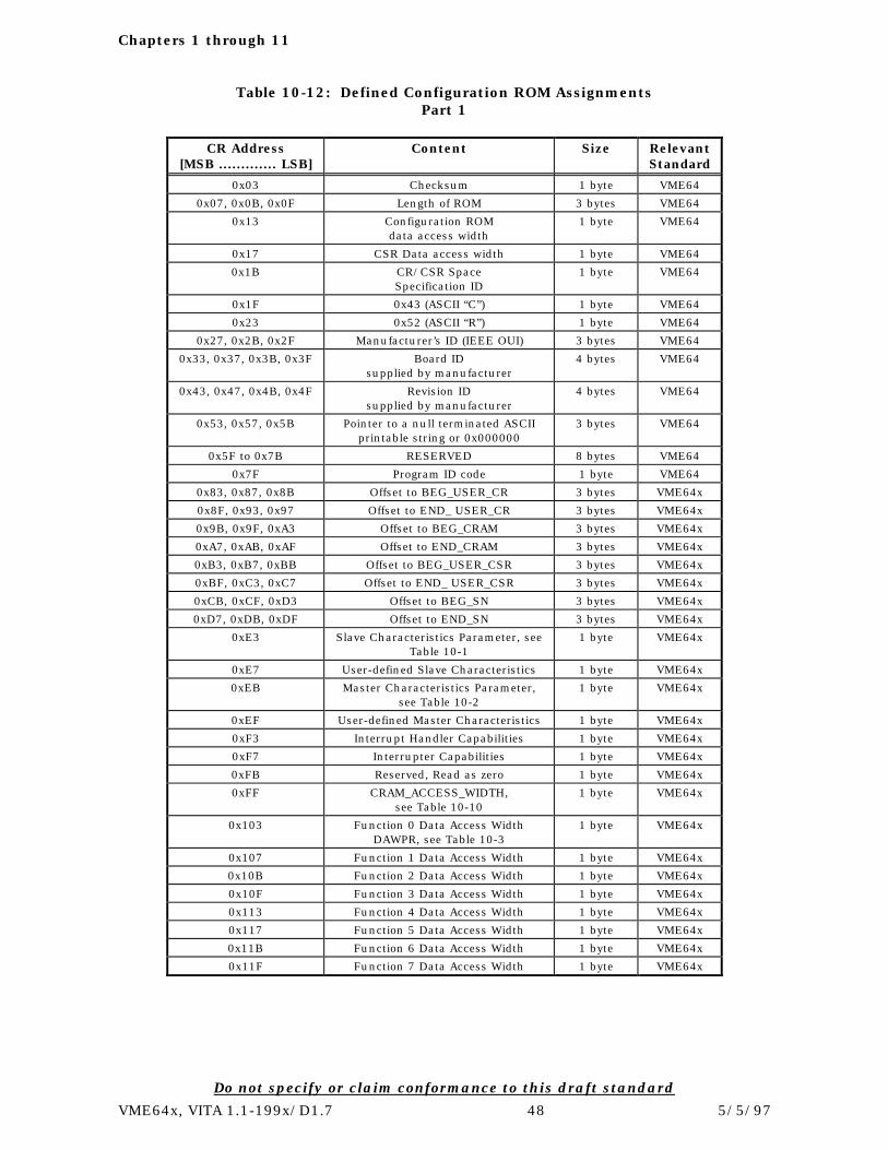
Chapters 1 through 11
Do not specify or claim conformance to this draft standard
VME64x, VITA 1.1-199x/D1.7 48 5/5/97
Table 10-12: Defined Configuration ROM AssignmentsPart 1
CR Address[MSB ............. LSB]
Content Size RelevantStandard
0x03 Checksum 1 byte VME64
0x07, 0x0B, 0x0F Length of ROM 3 bytes VME64
0x13 Configuration ROMdata access width
1 byte VME64
0x17 CSR Data access width 1 byte VME64
0x1B CR/CSR SpaceSpecification ID
1 byte VME64
0x1F 0x43 (ASCII “C”) 1 byte VME64
0x23 0x52 (ASCII “R”) 1 byte VME64
0x27, 0x2B, 0x2F Manufacturer’s ID (IEEE OUI) 3 bytes VME64
0x33, 0x37, 0x3B, 0x3F Board IDsupplied by manufacturer
4 bytes VME64
0x43, 0x47, 0x4B, 0x4F Revision IDsupplied by manufacturer
4 bytes VME64
0x53, 0x57, 0x5B Pointer to a null terminated ASCIIprintable string or 0x000000
3 bytes VME64
0x5F to 0x7B RESERVED 8 bytes VME64
0x7F Program ID code 1 byte VME64
0x83, 0x87, 0x8B Offset to BEG_USER_CR 3 bytes VME64x
0x8F, 0x93, 0x97 Offset to END_ USER_CR 3 bytes VME64x
0x9B, 0x9F, 0xA3 Offset to BEG_CRAM 3 bytes VME64x
0xA7, 0xAB, 0xAF Offset to END_CRAM 3 bytes VME64x
0xB3, 0xB7, 0xBB Offset to BEG_USER_CSR 3 bytes VME64x
0xBF, 0xC3, 0xC7 Offset to END_ USER_CSR 3 bytes VME64x
0xCB, 0xCF, 0xD3 Offset to BEG_SN 3 bytes VME64x
0xD7, 0xDB, 0xDF Offset to END_SN 3 bytes VME64x
0xE3 Slave Characteristics Parameter, seeTable 10-1
1 byte VME64x
0xE7 User-defined Slave Characteristics 1 byte VME64x
0xEB Master Characteristics Parameter,see Table 10-2
1 byte VME64x
0xEF User-defined Master Characteristics 1 byte VME64x
0xF3 Interrupt Handler Capabilities 1 byte VME64x
0xF7 Interrupter Capabilities 1 byte VME64x
0xFB Reserved, Read as zero 1 byte VME64x
0xFF CRAM_ACCESS_WIDTH,see Table 10-10
1 byte VME64x
0x103 Function 0 Data Access WidthDAWPR, see Table 10-3
1 byte VME64x
0x107 Function 1 Data Access Width 1 byte VME64x
0x10B Function 2 Data Access Width 1 byte VME64x
0x10F Function 3 Data Access Width 1 byte VME64x
0x113 Function 4 Data Access Width 1 byte VME64x
0x117 Function 5 Data Access Width 1 byte VME64x
0x11B Function 6 Data Access Width 1 byte VME64x
0x11F Function 7 Data Access Width 1 byte VME64x

Chapters 1 through 11
Do not specify or claim conformance to this draft standard
VME64x, VITA 1.1-199x/D1.7 49 5/5/97
Table 10-12: Defined Configuration ROM AssignmentsPart 2
CR Address[MSB ............. LSB]
Content Size RelevantStandard
0x123 … 0x13F Function 0 AM Code MaskAMCAP, see Table 10-5
8 bytes VME64x
0x143 … 0x15F Function 1 AM Code Mask 8 bytes VME64x
0x163 … 0x17F Function 2 AM Code Mask 8 bytes VME64x
0x183 … 0x19F Function 3 AM Code Mask 8 bytes VME64x
0x1A3 … 0x1BF Function 4 AM Code Mask 8 bytes VME64x
0x1C3 … 0x1DF Function 5 AM Code Mask 8 bytes VME64x
0x1E3 … 0x1FF Function 6 AM Code Mask 8 bytes VME64x
0x203 … 0x21F Function 7 AM Code Mask 8 bytes VME64x
0x223 … 0x29F Function 0 XAM Code MaskXAMCAP, see Table 10-5
32 bytes VME64x
0x2A3 … 0x31F Function 1 XAM Code Mask 32 bytes VME64x
0x323 … 0x39F Function 2 XAM Code Mask 32 bytes VME64x
0x3A3 … 0x41F Function 3 XAM Code Mask 32 bytes VME64x
0x423 … 0x49F Function 4 XAM Code Mask 32 bytes VME64x
0x4A3 … 0x51F Function 5 XAM Code Mask 32 bytes VME64x
0x523 … 0x59F Function 6 XAM Code Mask 32 bytes VME64x
0x5A3 … 0x61F Function 7 XAM Code Mask 32 bytes VME64x
0x623 … 0x62F Function 0 Address Decoder MaskADEM, see Table 10-4
4 bytes VME64x
0x633 … 0x63F Function 1 ADEM 4 bytes VME64x
0x643 … 0x64F Function 2 ADEM 4 bytes VME64x
0x653 … 0x65F Function 3 ADEM 4 bytes VME64x
0x663 … 0x66F Function 4 ADEM 4 bytes VME64x
0x673 … 0x67F Function 5 ADEM 4 bytes VME64x
0x683 … 0x68F Function 6 ADEM 4 bytes VME64x
0x693 … 0x69F Function 7 ADEM 4 bytes VME64x
0x6A3 Reserved, read as zero 1 byte VME64x
0x6A7 Reserved, read as zero 1 byte VME64x
0x6AB Reserved, read as zero 1 byte VME64x
0x6AF Master Data Access WidthDAWPR, see Table 10-3
1 byte VME64x
0x6B3 … 0x6CF Master AM CapabilityAMCAP, see Table 10-5
8 bytes VME64x
0x6D3 … 0x74F Master XAM CapabilityXAMCAP, see Table 10-5
32 bytes VME64x
0x753 … 0xFFF RESERVED 552 bytes VME64x

Chapters 1 through 11
Do not specify or claim conformance to this draft standard
VME64x, VITA 1.1-199x/D1.7 50 5/5/97
Table 10-13: Defined Control/Status Register (CSR) Assignments
CSR Address[MSB ............. LSB]
Content Size RelevantStandard
0x7FFFF CR/CSR (BAR)Base Address Register
1 byte VME64
0x7FFFB Bit Set Registersee Table 10-6
1 byte VME64
0x7FFF7 Bit Clear Registersee Table 10-7
1 byte VME64
0x7FFF3 CRAM_OWNER Register 1 byte VME64x
0x7FFEF User-Defined Bit SetRegister
1 byte VME64x
0x7FFEB User-Defined Bit ClearRegister
1 byte VME64x
0x7FFE3 ... 0x7FFE7 RESERVED 2 bytes VME64x
0x7FFD3 … 0x7FFDF Function 7 ADERsee Table 10-8
4 bytes VME64x
0x7FFC3 … 0x7FFCF Function 6 ADER 4 bytes VME64x
0x7FFB3 … 0x7FFBF Function 5 ADER 4 bytes VME64x
0x7FFA3 … 0x7FFAF Function 4 ADER 4 bytes VME64x
0x7FF93 … 0x7FF9F Function 3 ADER 4 bytes VME64x
0x7FF83 … 0x7FF8F Function 2 ADER 4 bytes VME64x
0x7FF73 … 0x7FF7F Function 1 ADER 4 bytes VME64x
0x7FF63 … 0x7FF6F Function 0 ADER 4 bytes VME64x
0x7FC00 … 0x7FF5F RESERVED 216 bytes VME64x
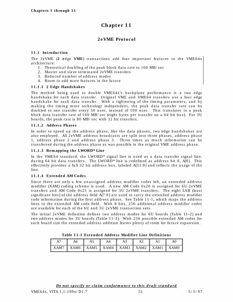
Chapters 1 through 11
Do not specify or claim conformance to this draft standard
VME64x, VITA 1.1-199x/D1.7 51 5/5/97
Chapter 11
2eVME Protocol
11.1 Introduction
The 2eVME (2 edge VME) transactions add four important features to the VME64xarchitecture:
1. Theoretical doubling of the peak block data rate to 160 MB/sec2. Master and slave terminated 2eVME transfers3. Reduced number of address modes4. Room to add more features in the future
11.1.1 2 Edge Handshakes
The method being used to double VME64x's backplane performance is a two edgehandshake for each data transfer. Original VME and VME64 transfers use a four edgehandshake for each data transfer. With a tightening of the timing parameters, and bymaking the timing more technology independent, the peak data transfer rate can bedoubled to one transfer every 50 nsec, instead of 100 nsec. This translates to a peakblock data transfer rate of 160 MB/sec (eight bytes per transfer on a 64 bit bus). For 3Uboards, the peak rate is 80 MB/sec with 32 bit transfers.
11.1.2 Address Phases
In order to speed up the address phase, like the data phases, two edge handshakes arealso employed. All 2eVME address broadcasts are split into three phases, address phase1, address phase 2 and address phase 3. Three times as much information can betransferred during the address phase as was possible in the original VME address phase.
11.1.3 Remapping the LWORD* Line
In the VME64 standard, the LWORD* signal line is used as a data transfer signal line,during 64 bit data transfers. The LWORD* line is redefined as address bit 0, A[0]. Thiseffectively provides a full 32 bit address bus, labeled A[31:0] and reflects the usage of theline.
11.1.4 Extended AM Codes
Since there are only a few unassigned address modifier codes left, an extended addressmodifier (XAM) coding scheme is used. A new AM Code 0x20 is assigned for 6U 2eVMEtransfers and AM Code 0x21 is assigned for 3U 2eVME transfers. The eight LSB (leastsignificant bits) of the address field A[7:0] are used to carry the extended address modifiercode information during the first address phase. See Table 11-1, which maps the addresslines to the extended AM code field. With 8 bits, 256 additional address modifier codesare available for each of the 6U and 3U 2eVME transaction sets.
The initial 2eVME definition defines two address modes for 6U boards (Table 11-2) andtwo address modes for 3U boards (Table 11-3). With 256 possible extended AM codes foreach board size the extended address addition leaves plenty of room for future expansion.
Table 11-1 Extended Address Modifier Line Definitions
A7 A6 A5 A4 A3 A2 A1 A0
XAM7 XAM6 XAM5 XAM4 XAM3 XAM2 XAM1 XAM0
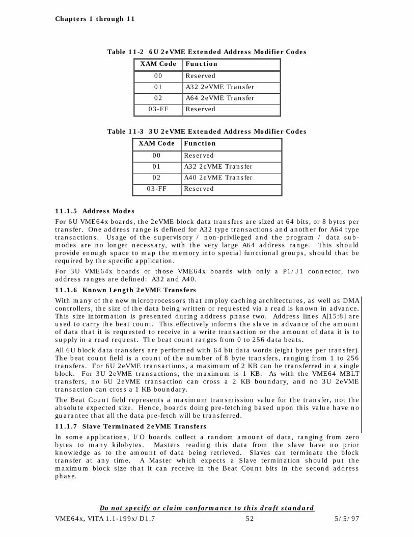
Chapters 1 through 11
Do not specify or claim conformance to this draft standard
VME64x, VITA 1.1-199x/D1.7 52 5/5/97
Table 11-2 6U 2eVME Extended Address Modifier Codes
XAM Code Function
00 Reserved
01 A32 2eVME Transfer
02 A64 2eVME Transfer
03-FF Reserved
Table 11-3 3U 2eVME Extended Address Modifier Codes
XAM Code Function
00 Reserved
01 A32 2eVME Transfer
02 A40 2eVME Transfer
03-FF Reserved
11.1.5 Address Modes
For 6U VME64x boards, the 2eVME block data transfers are sized at 64 bits, or 8 bytes pertransfer. One address range is defined for A32 type transactions and another for A64 typetransactions. Usage of the supervisory / non-privileged and the program / data sub-modes are no longer necessary, with the very large A64 address range. This shouldprovide enough space to map the memory into special functional groups, should that berequired by the specific application.
For 3U VME64x boards or those VME64x boards with only a P1/J1 connector, twoaddress ranges are defined: A32 and A40.
11.1.6 Known Length 2eVME Transfers
With many of the new microprocessors that employ caching architectures, as well as DMAcontrollers, the size of the data being written or requested via a read is known in advance.This size information is presented during address phase two. Address lines A[15:8] areused to carry the beat count. This effectively informs the slave in advance of the amountof data that it is requested to receive in a write transaction or the amount of data it is tosupply in a read request. The beat count ranges from 0 to 256 data beats.
All 6U block data transfers are performed with 64 bit data words (eight bytes per transfer).The beat count field is a count of the number of 8 byte transfers, ranging from 1 to 256transfers. For 6U 2eVME transactions, a maximum of 2 KB can be transferred in a singleblock. For 3U 2eVME transactions, the maximum is 1 KB. As with the VME64 MBLTtransfers, no 6U 2eVME transaction can cross a 2 KB boundary, and no 3U 2eVMEtransaction can cross a 1 KB boundary.
The Beat Count field represents a maximum transmission value for the transfer, not theabsolute expected size. Hence, boards doing pre-fetching based upon this value have noguarantee that all the data pre-fetch will be transferred.
11.1.7 Slave Terminated 2eVME Transfers
In some applications, I/O boards collect a random amount of data, ranging from zerobytes to many kilobytes. Masters reading this data from the slave have no priorknowledge as to the amount of data being retrieved. Slaves can terminate the blocktransfer at any time. A Master which expects a Slave termination should put themaximum block size that it can receive in the Beat Count bits in the second addressphase.
Chapters 1 through 11
Do not specify or claim conformance to this draft standard
VME64x, VITA 1.1-199x/D1.7 53 5/5/97
The 6U Slaves indicates this termination by asserting RETRY* and then asserting BERR*.The 3U Slaves indicates this termination by asserting RESP* and then asserting BERR*.This termination method tells the Master that the Slave has no more data and is notexpecting a resumption of that transfer.
11.1.8 Slave Suspended 2eVME Transfers
Large 2eVME transfers can be divided into smaller blocks by the slave, simply byterminating the block transfer after a few transfers. Masters can resume the blocktransfer at the next logical address. Slaves issuing the suspension indicate to the Masterthat more data can be transferred, just not at this time.
At times a slave board becomes busy and is unable to service a read or write request. Thismay be due to the resource, such as a dual port memory, being busy, or maybe its inputbuffer is still full, or whatever. The slave board can signal the requesting master to retrythe transaction a little later. In some applications, the master may not rerun a slaveterminated transaction, but just go on to the next task.
This same mechanism also works for deadlock resolution. Should one board’s master bein the process of trying to access another board's resource through a bridge, and at thesame time the other board's master is trying to access the first board's resource via thesame bridge, one of the masters must back off. Using the suspend protocol the bridgebetween the two buses can request one of the two masters to back off and try again,thereby resolving a possible deadlock situation.
6U Slaves requests that a master suspend a transaction by asserting RETRY* and thentoggling DTACK*. 3U Slaves requests that a master suspend a transaction by assertingRESP* and then toggling DTACK*. The suspend termination tells the Master that theSlave is stopping this transaction but is expecting a resumption of that transfer at a latertime. Suspended transactions always occur on an even beat count
11.1.9 Slave Error State
Slaves which detect an error can signal this condition to the Master by asserting BERR* inresponse to a transition of DS0* or DS1*. This is similar to the current BERR* usage inVME.
11.1.10 Master Terminated 2eVME Transfers
By definition, the master controls the size of each block transfer, by specifying the beatcount. The 2eVME protocol is designed to allow for early master termination, even beforethe beat count is reached (decremented to zero). This can be used for a variety of specialtype applications and situations. When the Master terminates it is always on an evenbeat count.
11.2 Requirements
11.2.1 Transceivers and Connectors
Permission 11.1:The 2eVME protocol may be operated in any VME or VME64x compliant backplane,using any VME or VME64x compliant logic family, which provides for monotonicswitching of control lines and meets the timing requirements of Table 11-6."
Observation 11.1:The RESP* signal is in the z row of the 160 pin connector, therefore the 160 connectormust be used to run the 2eVME protocol on 3U boards. 6U boards running the2eVME protocol can use with the 96 or 160 pin connectors.
11.2.2 Extended AM Codes
Rule 11.1:All 6U VME64x boards that perform 2eVME transactions shall use AM Code 0x20 and
Chapters 1 through 11
Do not specify or claim conformance to this draft standard
VME64x, VITA 1.1-199x/D1.7 54 5/5/97
shall use the extended AM Codes as defined in Table 11-2, 6U 2eVME Extended AMCodes.
Rule 11.2:All 3U VME64x boards that perform 2eVME transactions shall use AM Code 0x21 andshall use the extended AM Codes as defined in Table 11-3, 3U 2eVME Extended AMCodes.
Permission 11.2:6U VME64x boards may also participate in 3U 2eVME transfers using the applicableAM and XAM Codes defined for 3U 2eVME transfers.
11.2.3 Data Size
Rule 11.10:The maximum number of data beats shall be 256.
Observation 11.3:Rule 11.10 limits the data transferred to 2 KB, i.e. 256 beats x 8 bytes in a 6U VME64xboard and 1 KB in a 3U VME64x board.
Rule 11.4:A 6U 2eVME transfer shall not cross a 2 KB boundary and a 3U 2eVME transfer shallnot cross a 1 KB boundary.
Rule 11.5:All address and data lines shall be a logical zero for features which are notimplemented or are part of Reserved fields.
Rule 11.6:The beat count shall be sent in A[15:8] during the second address phase. The value isthe number of beats divided by two. For example 0x00 = none, 0x01 = 2 beats, .....0x80 = 256 beats.
Rule 11.7:Beat counts 0x81 through 0xFE shall be reserved.
Observation 11.3:Since the master can only do even beats for master terminated block transfers themodulo 2 number for the beat count is compatible with the specified operation.
Rule 11.8:The beat count shall be set to 0xFF as a default value when slave termination isexpected and the beat count is unknown.
Suggestion 11.1:The slave may use the beat count in a read operation to prefetch the required wordsand thereby increase performance.
Rule 11.9:The beat count represents a maximum value only. Slaves shall always be prepared foran early termination by the master during 2eVME transfers.
11.2.4 Protocols - General
Permission 11.3:Usage of both the RESP* and RETRY* signals is optional by both the master and theslave.
Observation 11.4:RESP* and RETRY* is used as a qualifier on the meaning of a timing response line.
Permission 11.4:RESP* is used by 3U boards and RETRY* by 6U boards. 6U master boards are givenpermission to use RESP* when communicating with 3U boards.

Chapters 1 through 11
Do not specify or claim conformance to this draft standard
VME64x, VITA 1.1-199x/D1.7 55 5/5/97
Rule 11.10:In 2eVME protocols only one timing (DS*) line shall transition in any one bus cycleexcept when the transaction is ended.
Rule 11.11:In 2eVME protocols only one timing response (DTACK* or BERR*) line shall transitionin any bus cycle except when the transaction is ended.
Observation 11.5:The support of slave terminated and slave suspended operations are not mandatory foreither masters of slaves.
Recommendation 11.1:Designs for masters conforming to the VME64x draft standard should implement slaveterminated and slave suspend operations.
Rule 11.12:The master timeout timer shall be set to "T".
Observation 11.6:The timeout value is one half the bus monitor BTO value. See VME64 Standard forfull explanation.
11.2.5 Timing
Rule 11.13:The timing of all 2eVME transactions shall be in accordance with the timingparameters defined in Table 11-6 and 11-7, 2eVME Specific and VME64 TimingParameters.
Rule 11.14:For each of the specific 2eVME transactions implemented, the protocol sequence shallbe in accordance to the respective transaction presented in Figures 11-1 through 11-12.
Rule 11.15:The strobing of information driven onto the backplane shall only occur after all thesignal lines have reached the required high or low signal level, as measured on thesource board connector. The values shall be as in Table 11-6 and 11-7.
Rule 11.16:All receivers of information transferred across the backplane shall compensate forbackplane skew, its own receiver skew, and an appropriate set up time before latchingthe transferred information. The values shall be as in Tables 11-6 and 11-7.
11.2.6 Address Phase Protocol and Timing
Rule 11.17:Starting addresses shall be aligned on 16 byte boundaries (i.e. 128 bit aligned).
Rule 11.18:Address timing and protocols shall be as defined in Figures 11-1 through 11-4.
Rule 11.19:BERR* can only be asserted on the first or third address phase instead of togglingDTACK*. See Figures 11-3 and 11-4.
Rule 11.20:DTACK* shall be the only valid responses during address phase 2.
Rule 11.21:Masters shall ignore the RETRY*/RESP* and BERR* during address phase 2.
Observation 11.7:Slave terminated and slave suspend operations are not supported during addressphase 2. Anomalous behavior can result if these responses are sent.
Chapters 1 through 11
Do not specify or claim conformance to this draft standard
VME64x, VITA 1.1-199x/D1.7 56 5/5/97
Observation 11.8:RESP* can be asserted only in the third address phase.
Observation 11.9:If RESP* is asserted before DTACK* is toggled on the third address phase the Masterinterprets that response as indicating that the Slave is suspending the operation butthe Master can expect data when it tries again. This can also be interpreted as a Slavesuspend response. See Figure 11-2.
Observation 11.10:If RESP* is asserted before BERR* is asserted in the third address phase the Masterinterprets that response as indicating that the Slave has no data and the transferattempt is to be terminated. See Figure 11-3.
Observation 11.11:Since the target address is in two parts the target device generates DTACK* during thefirst phase of the address cycle if that portion of the address is recognized. The lowestbyte of the address comes in the second address phase and therefore cannot be usedfor the address of the target device. The low byte only specifies an internal address.
Rule 11.22:Address lines A[20:16] in the second address phase shall provide the GA of the Masteras defined in Chapter 3 of this draft standard. If not implemented the value shall be0x00.
Observation 11.12:The GA in the second address phase provides a mechanism to determine the busmaster for a particular transaction.
Rule 11.23:Address lines A[31:24] in the second address phase shall provide a subunit number ofthe master. If not implemented the value shall be 0x00.
Observation 11.13:The subunit number provides a mechanism for identifying which part of a masterinitiated a transaction. In the case of a VME module with several processors it couldbe the processor number.
11.2.7 Data Phase Protocol and Timing
Rule 11.24:Data timing and protocols shall be as defined in Figures 11-5 through 11-12.
Observation 11.14:If RESP* is asserted before DTACK* is toggled during the data phase then the Masterinterprets that response as indicating that the Slave is suspending the operation butthe Master can expect data when it tries again. This can also be interpreted as a Slavebusy response. Data was not accepted or sent for that DS1* transition. See Figures11-6 and 11-10.
Observation 11.15:If RESP* is asserted before BERR* is asserted during the data phase then the Masterinterprets that response as indicating that the Slave has no data at that time and isfinished. Data was not accepted or sent for that DS1* transition. See Figures 11-7,11-8, 11-11 and 11-12.
Observation 11.16:The toggling of DTACK* without the assertion of RESP* during the data phaseindicates that the Slave has accepted the read or write data. See Figures 11-5 and 11-9.
Observation 11.17:The assertion of BERR* without RESP* during the data phase indicates that the Slavehas had an error and the data was not accepted or sent for that DS1* transition. SeeFigures 11-7, 11-8, 11-11 and 11-12.

Chapters 1 through 11
Do not specify or claim conformance to this draft standard
VME64x, VITA 1.1-199x/D1.7 57 5/5/97
Observation 11.18:Some bus timers are designed to assert BERR when DS0 or DS1 has been asserted forgreater than a set period, without monitoring the state of DTACK. In such a case, thebus timer could time-out a 2eVME transfer since DS1* is held low for the duration ofthe transfer. To avoid this, the bus timer should be set to a value greater than thelongest expected 2eVME transfer.
Rule 11.25:Master and Slave 2eVME state machines must be robust enough to recover gracefullyif BERR* is asserted by the bus time during a 2eVME transfer.
Table 11-4 6U VME64x Signal Field Definitions
AddressPhase 1
AddressPhase 2
AddressPhase 3
DataPhase
AM[5:0] 0x20 0x20 0x20 0x20
A[7:0] XAM Code(Table 11-2)
Internal AddressA[7:0]
Reserved D[39:32]
A[15:8] Device AddressA[15:8]
Beat Count Reserved D[47:40]
A[23:16] Device AddressA[23:16]
A[23:21] = 0A[20:16] = GA
of Master
Reserved D[55:48]
A[31:24] Device AddressA[31:24]
A[31:24] = Subunitnumber in Master
Reserved D[63:56]
D[31:0] Device AddressA[63:32] (= 0 for A32)
Reserved Reserved D[31:0]
Table 11-5 3U VME64x Signal Field Definitions
AddressPhase 1
AddressPhase 2
AddressPhase 3
DataPhase
AM[5:0] 0x21 0x21 0x21 0x21
A[7:0] XAM Code(Table 11-3)
Internal AddressA[7:0]
Reserved D[23:16]
A[15:8] Device Address A[15:8] Beat Count Reserved D[31:24]
A[23:16] Device AddressA[23:16]
A[23:21] = 0A[20:16] = GA
of Master
Reserved Reserved
D[7:0] Device AddressA[31:24]
D[7:0] = Subunitnumber in Master
Reserved D[7:0]
D[15:8] Device AddressA[39:32] (= 0 for A32)
Reserved Reserved D[15:8]

Chapters 1 through 11
Do not specify or claim conformance to this draft standard
VME64x, VITA 1.1-199x/D1.7 58 5/5/97
Table 11-6 2eVME Specific Timing Parameters
TimingParameter
Description Source(ns)
Destination(ns)
S1 Address and data setup time 0 -21
S2 RESP* to DTACK*/BERR* setup time 20 10
H1 Address or Data hold time 0 0
T1 Handshake delay time 0 0
Table 11-7 2eVME Timing Parameters
TimingParameter
Description At MASTER(ns)
At SLAVE(ns)
4 IACK*, AM[5:0], & Address valid toAS* assertion setup time 35 10
6 Time from DTACK* high to time datalines can be driven by MASTER 0 0
7 Delay time from data line release toMASTER assertion of DS1*
(begin Data Phase)0 0
8 Data line setup time to DS0*/DS1* 35 10
10 Delay time from AS* tofirst assertion of DS0*/DS1* 0 -10
12 WRITE* valid to DS0*/DS1* setuptime
35 10
16 IACK* and AM[5:0] hold time from lastassertion of DTACK* or BERR*
0 0
18A AS* negation time from lastDTACK* or BERR*
0 0
23 WRITE* hold time from last negationof DS0*/DS1*
10 0
26 Delay from first assertion of DS1* toSLAVE assertion of data lines
0 0
31 Delay from data line release untilSLAVE can drive/release DTACK* or
BERR* at end of read data phase
0 0
Chapters 1 through 11
Do not specify or claim conformance to this draft standard
VME64x, VITA 1.1-199x/D1.7 59 5/5/97
The following figures are attached to the end of this draft standard.
None of the figures were update from draft 1.5 and draft 1.6, except forfigure numbers, titles and page numbers
Figure 11-1 2eVME Address Broadcast
Figure 11-2 2eVME Address Broadcast - Slave Suspend Response
Figure 11-3 2eVME Address Broadcast - Slave Stop/Error Response
Figure 11-4 2eVME Address Broadcast - Slave Suspend/Stop/Error Response
Figure 11-5 2eVME Read Data Transfers - Master termination
Figure 11-6 2eVME Read Data Transfers - Slave Suspend
Figure 11-7 2eVME Read Data Transfers - Slave Stop/Error on Odd Beat
Figure 11-8 2eVME Read Data Transfers - Slave Stop/Error on Even Beat
Figure 11-9 2eVME Write Data Transfers - Master Termination
Figure 11-10 2eVME Write Data Transfers - Slave Suspend
Figure 11-11 2eVME Write Data Transfers - Slave Stop/Error on Odd Beat
Figure 11-12 2eVME Write Data Transfers - Slave Stop/Error on Even Beat

Appendix A through D
Do not specify or claim conformance to this draft standard
VME64x, VITA 1.1-199x/D1.7 60 5/5/97
Appendix A
Glossary of Additional VME64x Terms
Introduction
This is an extension of the terms defined in the VME64 Standard, Appendix A.Terminology described in the VME64 Standard are not repeated in this standard. Refer tothe VME64 Standard for a listing of the VME64 Terminology.
3UA term used to describe single high VME, VME64 and VME64x boards that are 100mm in height. Also used to describe backplanes that interface to these sameboards.
6UA term used to describe double high VME, VME64 and VME64x boards that are233.35 mm in height. Also used to describe backplanes that interface to thesesame boards.
9UA term used to describe triple high boards that are 366.70 mm in height. Alsoused to describe backplanes that interface to these same boards. 9U VME, VME64and VME64x boards and backplanes are not defined in this draft standard, but aregenerally considered an optional size.
* (asterisk)When appended to a signal's name, the suffix "*" indicates that the logic state ofthe signal is the opposite state. A high is a logic zero and a low is a logic one.
Address Space RelocationThe ability to change the base address of a contiguous area within a module.Traditionally in VME, this has been done manually with jumpers or switches.Chapter 10 of this document specifies support for software-programmable addressspace relocation, thus supporting "plug and play" on VME. Also specified is astandard way to latch switch settings for software to read.
Amnesia AddressAn address value used when a geographical address parity error is detected. Theboard does not know its real geographical address, therefore assigns itself apredefined address value stating "I am alive, but don't know the correct slotnumber".
BARBase Address Register in the CR/CSR. The value is set by the geographicaladdress pins or via the auto slot identification function.
Configuration RAM (CRAM)This optional area within CR/CSR space may provide "scratch pad" RAM for use bysystem software. The intended use is storage of configuration data associated withthe module, such as driver state data to enable automatic fail over.
ContactA term used to describe the physical connection within a connector where twomechanical components mate to provide an electrical path between two matingelements, such as a board to a backplane or a cable to board.
Appendix A through D
Do not specify or claim conformance to this draft standard
VME64x, VITA 1.1-199x/D1.7 61 5/5/97
Data BeatA time period in which a unit of data is transferred from the source to thedestination in the 2eVME protocol. The unit of data is either 4 or 8 bytes.
Geographical Addressing An address mechanism which provides the binary number of the board slot.
Mate First Break Last (MFBL)A set of one or more pins that contact before other pin(s) within a connector orconnector group during connector mating, i.e. they mate first. During thedisconnection of a connector pair, the set of one or more pins that break contactlast.
MonarchThe processor that gains or is assigned control to manage the initialization andconfiguration of all boards plugged into the backplane. The monarch may also bethe processor that manages the total system during normal operation.
P0/J0 Connector AreaA term used to describe the area on VME64x boards between the P1 and P2connectors and on VME64 backplanes between the J1 and J2 connectors. Thearea is used to mount additional connectors for user defined I/O off VME64xboards through VME64x backplanes.
PinsA term used to describe a connectors physical mechanism of connecting a signalbetween a board and backplane. The expanded IEC 603-2 connector, providesadditional contacts on the connector's outer shell. These are physically blade-on-beam style contacts. Within this standard, the term "pin" is also used to representthese connector contacts.
PositionA term used to describe the "short row" of pins in a connector which runs theshorter length of the connector, such as pins z17, a17, b17, c17 and d17.
Precharge voltageA voltage supplied to the board prior to a board's signal pins contact with thebackplane connectors. This voltage is used to precharge bus signal pins on theboard and to put the bus transceivers into a high impedance mode prior to liveinsertion. This voltage is also used by the hot swap control logic. This voltage isalso used during the withdrawal of a board from a backplane.
RowA term used to describe the set of pins in a connector which run the longer lengthof the connector.
User Defined I/OA term used to describe the functional definition of a group of connector I/O signalpins. The user in this case can be either the supplier (manufacturer) of the boardor the end user of the board. From a "standards" point of view, both are users ofthe standard, therefore the broad definition of "user defined".
User SpaceA space within the CR/CSR address space where specific end user's applicationcode (program or data) can be placed. Suppliers (manufacturers) are not allowedto use this space.

Appendix A through D
Do not specify or claim conformance to this draft standard
VME64x, VITA 1.1-199x/D1.7 62 5/5/97
Appendix B
Additional VME64x Signal/Pin Descriptions
Introduction
This appendix describes the additional VME64x signal lines and associated connector pindefined in this draft standard. See the VME64 Standard, Appendix B for the VME64signal/pin descriptions. The following table identifies the VME64x signal/pin bymnemonic and describes the signal/pin characteristics.
VME64 Signal Identification
Signal/PinMnemonic Signal/Pin Name and Description
GA[4..0]* Geographical Address - A set of backplane driven signals that are either tiedto ground or floating and are used to carry slot number information.
GAP* Geographical Address Parity - A backplane driven signal that is either tiedto ground or floating and is used to carry geographical address parity.
GND The DC voltage reference and to carry the power return current for boardsand backplanes.
LI/I* Live Insertion Input - A three-state driven signal that is used to carry hotswap input control information.
LI/O* Live Insertion Output - A three-state driven signal that is used to carry hotswap output control information.
MCLK IEEE 1149.5 MTM-Bus Clock - A three-state driven signal that is used tocarry the T&Mbus clock signal.
MCTL IEEE 1149.5 MTM-Bus Control - A three-state driven signal that is used tocarry the T&Mbus control signal.
MMD IEEE 1149.5 MTM-Bus Master Data - A three-state driven signal that isused to carry the T&Mbus master data signal information.
MPR IEEE 1149.5 MTM-Bus Pause Request - A three-state driven signal that isused to carry the T&Mbus pause request signal information.
MSD IEEE 1149.5 MTM-Bus Slave Data - A three-state driven signal that isused to carry the T&Mbus slave data signal information.
RESP* Response - A three-state driven signal that is used to carry the Responsesignal information as defined by the 2eVME Protocol.
RsvB Reserved Bused - These reserved bused signals are reserved for futuredefinition by the VITA Standards Organization.
RsvU Reserved Unbused - These connector pins are reserved for future definitionby the VITA Standards Organization.
Appendix A through D
Do not specify or claim conformance to this draft standard
VME64x, VITA 1.1-199x/D1.7 63 5/5/97
Signal/PinMnemonic Signal /Pin Name and Description
SBA Serial Bus A Line - A three-state driven signal that is used to carry serialdata information for hot swap control.
SBB Serial Bus B Line - A three-state driven signal that is used to carry serialdata information for hot swap control.
UD User Defined - These pins are defined by the user and are used to carryvarious types of input/output information.
VPC Voltage PreCharge - A power voltage used by the hot swap logic.
+3.3V +3.3 VDC Power - Used by on board logic circuits.
+V1 The positive side of the 48 volt supply, usually paired with the +V2 powerpin.
+V2 The positive side of the 48 volt supply, usually paired with the +V1 powerpin.
-V1 The negative side of the 48 volt supply, usually paired with the -V2 powerpin.
-V2 The negative side of the 48 volt supply, usually paired with the -V1 powerpin.

Appendix A through D
Do not specify or claim conformance to this draft standard
VME64x, VITA 1.1-199x/D1.7 64 5/5/97
Appendix C
VME64 and VME64x Function Mnemonics
Introduction
This appendix lists the functional mnemonics of the VME64 Standard and this draftstandard. The signal/pin mnemonics listed in Appendix B are not included in thisappendix. These mnemonics can be used to describe the functional capability of VME,VME64 and VME64x boards, backplanes and systems, where appropriate.
Mnemonic Description
+12V Backplane or system provides +12V power or board uses +12V power
+3.3V Backplane or system provides +3.3V power or board uses +3.3V power
+5V Backplane or system provides +5V power or board uses +5V power
-12V Backplane or system provides -12V power or board uses -12V power
2eVME Board supports the 2eVME protocol
48V Backplane or system provides 48V power or board uses 48V power
A16 Performs 16 bit address transfers across the backplane
A24 Performs 24 bit address transfers across the backplane
A32 Performs 32 bit address transfers across the backplane
A40 Performs 40 bit address transfers across the backplane
A64 Performs 64 bit address transfers across the backplane
ADO Board supports address only cycles without handshakes
ADOH Board supports address only cycles with handshakes
BLT Performs block transfers across the backplane
BTO Provides the bus timer time out function
CR/CSR Board supports the CR/CSR function
D08 Performs 8 bit data transfers across the backplane
D16 Performs 16 bit data transfers across the backplane
D32 Performs 32 bit data transfers across the backplane
D64 Performs 64 bit data transfers across the backplane
ESD Subrack or board supports the VME64x ESD scheme
EMC Subrack or board supports the VME64x EMC scheme
ETL Board uses the ETL devices for bus transceivers
FAIR Bus requester supports the fair bus request mode
GA Uses or provides geographical address.
GAP Uses or provides geographical address parity
I(x) Interrupter, which generates interrupts on level x- Where x ranges between 1 to 7
IE/HDL Board uses the injection/extraction handles
IEL/HDL Board uses the injection/extraction/locking handles
IE/COMB Subrack provides the front rail comb for support of the injection/extractionhandles
Appendix A through D
Do not specify or claim conformance to this draft standard
VME64x, VITA 1.1-199x/D1.7 65 5/5/97
IH(x) Interrupt handler processes interrupt level x- Where x ranges between 1 to 7
IH(x-y) Interrupt handler processes interrupt levels x through y- Where x and y range between 1 to 7
J0 Backplane uses the 95 pin 2 mm connector in the J0 connector area
J0/S A special connector (e.g. fiber optic or coaxial) in the J0 connector area
J1/96 Backplane uses the 96 pin connector in the J1 connector area
J1/160 Backplane uses the 160 pin connector in the J1 connector area
J2/96 Backplane uses the 96 pin connector in the J2 connector area
J2/160 Backplane uses the 160 pin connector in the J2 connector area
KEY Subrack or board supports the VME64x keying scheme
Lock Board support the locked cycles
MBLT Performs multiplexed block transfers across the backplane
MTM Board supports the IEEE 1149.5 MTM function
P0 Board uses the 95 pin 2 mm connector in the P0 connector area
P0/S A special connector (e.g. fiber optic or coaxial) in the P0 connector area
P1/96 Board uses the 96 pin connector in the P1 connector area
P1/160 Board uses the 160 pin connector in the P1 connector area
P2/96 Board uses the 96 pin connector in the P2 connector area
P2/160 Board uses the 160 pin connector in the P2 connector area
PRI Bus arbiter supports the priority mode
RETRY Board supports protocols with retry capability
RESP Board support protocol with response capability
RMW Performs read-modify-write transfers across the backplane
ROR Bus requester supports the release-on-request mode
RRS Bus arbiter supports the round robin mode
RWD Bus requester supports the release-when-done mode
SysCon Provides the system controller functions including: BTO, arbitration,interrupt daisy chain driver and 16 MHz system clock driver
UAT Performs unaligned transfers across the backplane
VPC Backplane provides or board uses the pre-charge voltage power(Power provided or used shall be included in the +5V power ratings)
W+12:x Max +12V power provided by the backplane or system (in watts)- Or max. +12V power consumed by a board averaged over a one secondperiod
W-12:x Max -12V power provided by the backplane or system (in watts)- Or max. -12V power consumed by a board averaged over a one secondperiod
W+3.3:x Max +3.3V power provided by the backplane or system (in watts)- Or max. +3.3V power consumed by a board averaged over a one secondperiod
W+5:x Max +5V power provided by the backplane or system (in watts)- Or max. +5V power consumed by a board averaged over a one secondperiod
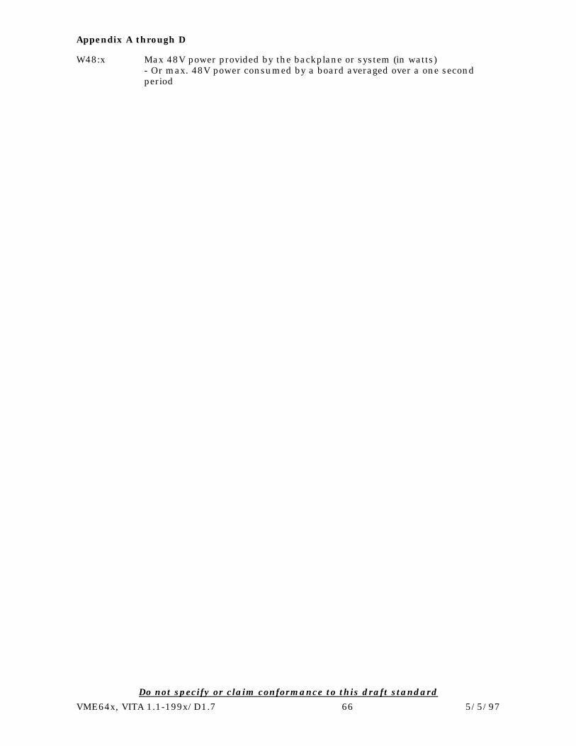
Appendix A through D
Do not specify or claim conformance to this draft standard
VME64x, VITA 1.1-199x/D1.7 66 5/5/97
W48:x Max 48V power provided by the backplane or system (in watts)- Or max. 48V power consumed by a board averaged over a one secondperiod
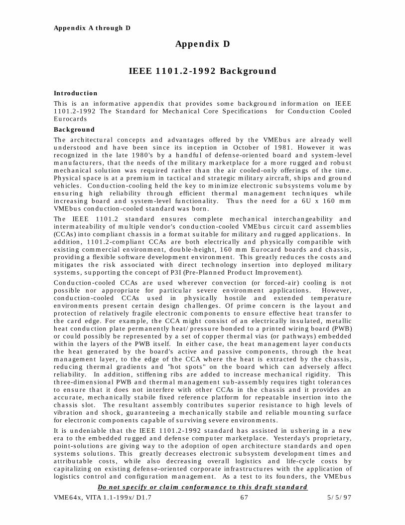
Appendix A through D
Do not specify or claim conformance to this draft standard
VME64x, VITA 1.1-199x/D1.7 67 5/5/97
Appendix D
IEEE 1101.2-1992 Background
Introduction
This is an informative appendix that provides some background information on IEEE1101.2-1992 The Standard for Mechanical Core Specifications for Conduction CooledEurocards
Background
The architectural concepts and advantages offered by the VMEbus are already wellunderstood and have been since its inception in October of 1981. However it wasrecognized in the late 1980's by a handful of defense-oriented board and system-levelmanufacturers, that the needs of the military marketplace for a more rugged and robustmechanical solution was required rather than the air cooled-only offerings of the time.Physical space is at a premium in tactical and strategic military aircraft, ships and groundvehicles. Conduction-cooling held the key to minimize electronic subsystems volume byensuring high reliability through efficient thermal management techniques whileincreasing board and system-level functionality. Thus the need for a 6U x 160 mmVMEbus conduction-cooled standard was born.
The IEEE 1101.2 standard ensures complete mechanical interchangeability andintermateability of multiple vendor's conduction-cooled VMEbus circuit card assemblies(CCAs) into compliant chassis in a format suitable for military and rugged applications. Inaddition, 1101.2-compliant CCAs are both electrically and physically compatible withexisting commercial environment, double-height, 160 mm Eurocard boards and chassis,providing a flexible software development environment. This greatly reduces the costs andmitigates the risk associated with direct technology insertion into deployed militarysystems, supporting the concept of P3I (Pre-Planned Product Improvement).
Conduction-cooled CCAs are used wherever convection (or forced-air) cooling is notpossible nor appropriate for particular severe environment applications. However,conduction-cooled CCAs used in physically hostile and extended temperatureenvironments present certain design challenges. Of prime concern is the layout andprotection of relatively fragile electronic components to ensure effective heat transfer tothe card edge. For example, the CCA might consist of an electrically insulated, metallicheat conduction plate permanently heat/pressure bonded to a printed wiring board (PWB)or could possibly be represented by a set of copper thermal vias (or pathways) embeddedwithin the layers of the PWB itself. In either case, the heat management layer conductsthe heat generated by the board's active and passive components, through the heatmanagement layer, to the edge of the CCA where the heat is extracted by the chassis,reducing thermal gradients and "hot spots" on the board which can adversely affectreliability. In addition, stiffening ribs are added to increase mechanical rigidity. Thisthree-dimensional PWB and thermal management sub-assembly requires tight tolerancesto ensure that it does not interfere with other CCAs in the chassis and it provides anaccurate, mechanically stabile fixed reference platform for repeatable insertion into thechassis slot. The resultant assembly contributes superior resistance to high levels ofvibration and shock, guaranteeing a mechanically stabile and reliable mounting surfacefor electronic components capable of surviving severe environments.
It is undeniable that the IEEE 1101.2-1992 standard has assisted in ushering in a newera to the embedded rugged and defense computer marketplace. Yesterday's proprietary,point-solutions are giving way to the adoption of open architecture standards and opensystems solutions. This greatly decreases electronic subsystem development times andattributable costs, while also decreasing overall logistics and life-cycle costs bycapitalizing on existing defense-oriented corporate infrastructures with the application oflogistics control and configuration management. As a test to its founders, the VMEbus
Appendix A through D
Do not specify or claim conformance to this draft standard
VME64x, VITA 1.1-199x/D1.7 68 5/5/97
continues to migrate and grow with technology advances, continually increasingperformance, bandwidth and functionality - while maintaining forward and backwardcompatibility - securing an enviable position of flourishing well into the next century.

Do not specify or claim conformance to this draft standardVME64x, VITA 1.1-199x/D1.7 69 5/5/97
AM[5..0]
A[31..1]
AS*
DS0*
DS1*
LWORD*
Extended AM Mode (Value = 20h or 21h)
AP1 Info AP2 Info
DTACK*
WRITE* HIGH for Read LOW for Write
2eM
BLT
DAT
A T
RA
NS
FE
RS
IACK*
D[31..0] AP1 Info AP2 Info
Figure 11-1 2eVME Address Broadcast
AP3 Info
AP3 Info
12
10
4
6
8
T1 H1
S1
T1 H1 H1
S1
T1T1 T1
16
T1
T1
18A
Do not specify or claim conformance to this draft standardVME64x, VITA 1.1-199x/D1.7 70 5/5/97
AM[5..0]
A[31..1]
AS*
DS0*
DS1*
LWORD*
Extended AM Mode (Value = 20h or 21h)
DTACK*
WRITE* HIGH for Read LOW for Write
IACK*
D[31..0]
RTRY1*
Figure 11-2 2eVME Address Broadcast - Slave Suspend Response
AP2 Info
AP1 Info AP2 Info
AP3 Info
AP3 Info
AP1 Info
6
S2
T1T1H1
T1
H1T1H1T1
8 S1 S1
4
10
12 16
18A

Do not specify or claim conformance to this draft standardVME64x, VITA 1.1-199x/D1.7 71 5/5/97
AM[5..0]
A[31..1]
AS*
DS0*
DS1*
LWORD*
Extended AM Mode (Value = 20h or 21h)
DTACK*
WRITE* HIGH for Read LOW for Write
IACK*
D[31..0]
RTRY1*
Figure 12-3 2eVME Address Broadcast - Slave Stop/Error Response
AP1 Info AP2 Info
AP1 Info AP2 Info
AP3 Info
AP3 Info
BERR*
4
10
12
6 T1 H1 T1 H1
8 S1 S1
T1
S2
H1 T1 T1
16
18A

Do not specify or claim conformance to this draft standardVME64x, VITA 1.1-199x/D1.7 72 5/5/97
AM[5..0]
A[31..1]
AS*
DS0*
DS1*
LWORD*
Extended AM Mode (Value = 20h or 21h)
DTACK*
WRITE* HIGH for Read LOW for Write
IACK*
D[31..0]
RTRY1*
Figure 12-4 2eVME Address Broadcast - Slave Suspend/Stop/Error Response
AP1 Info
AP1 Info
BERR*
4
10
12
6 T1
8
S2
H1 T1 T1
16
18A

Do not specify or claim conformance to this draft standardVME64x, VITA 1.1-199x/D1.7 73 5/5/97
A[31..1]
D[31..0]
DS0*
DS1*
LWORD*Data
Data
DTACK*
WRITE*
M S
M S INSERTREAD DATA
TRANSFERS AS SHOWN
BELOW
RTRY1*
Figure 12-5 2eVME Read Data Transfers - Master Termination
Odd
Odd
BERR*
A[31..1]
D[31..0]
DS0*
DS1*
LWORD*Odd Data
Odd Data
DTACK*
Even Data
Even Data
Odd Data
Odd Data
Even Data
Even Data
T1 H1
26
S1
H1
S1 T1
H1
23
31
S1 T1T1
H1
S1T1
H1
7

Do not specify or claim conformance to this draft standardVME64x, VITA 1.1-199x/D1.7 74 5/5/97
A[31..1]
D[31..0]
DS0*
DS1*
LWORD*
DTACK*
WRITE*
M S
M S
RTRY1*
INSERTREAD DATA
TRANSFERS AS SHOWN
BELOW
Figure 12-6 2eVME Read Data Transfers - Slave Suspend
Data
Data
Even Data
Even Data
BERR*
Odd
Odd
T1 H1 S1
H1 S1 T1 H1 31
23
S2
267
A[31..1]
D[31..0]
DS0*
DS1*
LWORD*Odd Data
Odd Data
DTACK*
Even Data
Even Data
Odd Data
Odd Data
S1 T1T1
H1
S1T1
H1

Do not specify or claim conformance to this draft standardVME64x, VITA 1.1-199x/D1.7 75 5/5/97
A[31..1]
D[31..0]
DS0*
DS1*
LWORD*Data
Data
DTACK*
WRITE*
M S
M S
Even Data
Even DataINSERTREAD DATA
TRANSFERS AS SHOWN
BELOW
RTRY1*
Figure 12-7 2eVME Read Data Transfers - Slave Stop/Error on Odd Beat
Odd
Odd
BERR*
T1 H1 S1
H1 S1
T1 T1 T1
T1 31
S2
H1
23
267
A[31..1]
D[31..0]
DS0*
DS1*
LWORD*Odd Data
Odd Data
DTACK*
Even Data
Even Data
Odd Data
Odd Data
S1 T1T1
H1
S1T1
H1
Do not specify or claim conformance to this draft standardVME64x, VITA 1.1-199x/D1.7 76 5/5/97
A[31..1]
D[31..0]
DS0*
DS1*
LWORD*
DTACK*
WRITE*
M S
M S
RTRY1*
INSERTREAD DATA
TRANSFERS AS SHOWN
BELOW
Figure 12-8 2eVME Read Data Transfers - Slave Stop/Error on Even Beat
Odd Data
Odd Data
BERR*
T1 H1 S1
T1H1 T1 31
23
S2
267
A[31..1]
D[31..0]
DS0*
DS1*
LWORD*Odd Data
Odd Data
DTACK*
Even Data
Even Data
Odd Data
Odd Data
S1 T1T1
H1
S1T1
H1
T1
Do not specify or claim conformance to this draft standardVME64x, VITA 1.1-199x/D1.7 77 5/5/97
Odd Data
Odd Data
A[31..1]
D[31..0]
DS0*
DS1*
LWORD*
DTACK*
WRITE*
INSERTWRITE DATATRANSFERS AS SHOWN
BELOW
A[31..1]
D[31..0]
DS0*
DS1*
LWORD*Even Data
Even Data
DTACK*
Odd Data
Odd Data
RTRY1*
Figure 12-9 2eVME Write Data Transfers - Master Termination
BERR*
Even Data
Even Data
S1 H1 S1 H1
T1T1
T1 H1
S1
T1 H1
S1
T1
H1 T1 T1
23
Do not specify or claim conformance to this draft standardVME64x, VITA 1.1-199x/D1.7 78 5/5/97
RTRY1*
Odd Data
Odd Data
A[31..1]
D[31..0]
DS0*
DS1*
LWORD*Even Data
Even Data
DTACK*
WRITE*
INSERTWRITE DATATRANSFERS AS SHOWN
BELOW
Figure 12-10 2eVME Write Data Transfers - Slave Suspend
BERR*
T1 H1
S1
T1 H1
S1
T1
S2
H1 T1 T1
23
A[31..1]
D[31..0]
DS0*
DS1*
LWORD*Even Data
Even Data
DTACK*
Odd Data
Odd Data
S1 H1 S1 H1
T1T1

Do not specify or claim conformance to this draft standardVME64x, VITA 1.1-199x/D1.7 79 5/5/97
RTRY1*
Odd Data
Odd Data
A[31..1]
D[31..0]
DS0*
DS1*
LWORD*Even Data
Even Data
DTACK*
WRITE*
INSERTWRITE DATATRANSFERS AS SHOWN
BELOW
Figure 12-11 2eVME Write Data Transfers - Slave Stop/Error on Odd Beat
BERR*
Odd Data
Odd Data
T1 H1
S1
T1 H1
S1 H1
T1
S1 H1 T1 T1
T1
S2
23
A[31..1]
D[31..0]
DS0*
DS1*
LWORD*Even Data
Even Data
DTACK*
Odd Data
Odd Data
S1 H1 S1 H1
T1T1

Do not specify or claim conformance to this draft standardVME64x, VITA 1.1-199x/D1.7 80 5/5/97
RTRY1*
Odd Data
Odd Data
A[31..1]
D[31..0]
DS0*
DS1*
LWORD*Even Data
Even Data
DTACK*
WRITE*
INSERTWRITE DATATRANSFERS AS SHOWN
BELOW
Figure 12-12 2eVME Write Data Transfers - Slave Stop/Eerror on Even Beat
BERR*
T1 H1
S1
T1 H1
S1
23
T1T1H1
T1
S2
A[31..1]
D[31..0]
DS0*
DS1*
LWORD*Even Data
Even Data
DTACK*
Odd Data
Odd Data
S1 H1 S1 H1
T1T1