Embed Size (px)
Citation preview
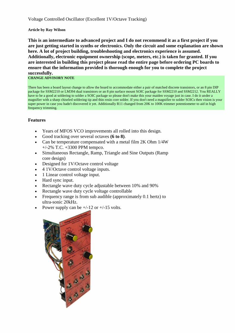
Voltage Controlled Oscillator (Excellent 1V/Octave Tracking)
Article by Ray Wilson
This is an intermediate to advanced project and I do not recommend it as a first project if you
are just getting started in synths or electronics. Only the circuit and some explanation are shown
here. A lot of project building, troubleshooting and electronics experience is assumed.
Additionally, electronic equipment ownership (scope, meters, etc.) is taken for granted. If you
are interested in building this project please read the entire page before ordering PC boards to
ensure that the information provided is thorough enough for you to complete the project
successfully. CHANGE ADVISORY NOTE
There has been a board layout change to allow the board to accommodate either a pair of matched discrete transistors, or an 8 pin DIP
package for SSM2210 or LM394 dual transistors or an 8 pin surface mount SOIC package for SSM2210 and SSM2212. You REALLY
have to be a good at soldering to solder a SOIC package so please don't make this your maiden voyage just in case. I do it under a
magnifier with a sharp chiseled soldering tip and thin rosin core solder. If you don't need a magnifier to solder SOICs then vision is your
super power in case you hadn't discovered it yet. Additionally R11 changed from 20K to 100K trimmer potentiometer to aid in high frequency trimming.
Features
Years of MFOS VCO improvements all rolled into this design.
Good tracking over several octaves (6 to 8).
Can be temperature compensated with a metal film 2K Ohm 1/4W
+/-2% T.C. +3300 PPM tempco.
Simultaneous Rectangle, Ramp, Triangle and Sine Outputs (Ramp
core design)
Designed for 1V/Octave control voltage
4 1V/Octave control voltage inputs.
1 Linear control voltage input.
Hard sync input.
Rectangle wave duty cycle adjustable between 10% and 90%
Rectangle wave duty cycle voltage controllable
Frequency range is from sub audible (approximately 0.1 hertz) to
ultra-sonic 20kHz.
Power supply can be +/-12 or +/-15 volts.

MP3 Samples
Sine wave with sequencer and keyboard
Sine wave with sequencer and keyboard
Triangle wave with sequencer and keyboard
Ramp wave with sequencer and keyboard
Square/Pulse with sequencer and keyboard
Sync Effects
Frequency Range Demonstration
Modulation with keyboard and LFO
Messing about with ramp waves (3 VCOs)
Messing about with square waves (3 VCOs)
Messing about with the sequencer attached (4 VCOs)
Messing about with the sequencer attached (4 VCOs)
Links to previous versions for reference
VCO200604REV01.html
VCO200503REV01.html
VCO20090724REV0.html
Introduction
Oscillators are the main tone generating modules of your synthesizer. This oscillator produces sine,
square, triangle and ramp waveforms and with careful adjustment tracks at 1V/octave over 6 to 8
octaves. The parts for it are easily obtained and not extremely expensive. The whole circuit is here so
breadboard it and see if you like it. I like this oscillator but please recognize that it relies on a well
matched pair of transistors. Its frequency range is from below audible to beyond audible. If this
oscillator meets your needs I have high quality PC boards for sale for this design.
Voltage Controlled Oscillator Schematic Page 1 PDF
+/-15V Users Take Note
While helping diyer Doug Slocum improve the tracking on his MFOS VCOs I found a few things +/-
15V users should change.
Change R46 to 1.54K metal film (1.5K carbon will be ok too). This sets the bias for the
comparator since it changes at +/-15V. This corrects the whole rest of the waveform chain's
amplitude.
Change R10 to 150K and R65 to 43K this will give you a better range on the coarse freq
control. Use metal film.
Change R28 to 1.5M metal film. Changes the starting current of the expo convertor to 1uA.
Use OP275 for U1. Its performance is superior to other op amps.
Make sure and use a 100K multi-turn for the high frequency adjust.

Page 1 shows the voltage to exponential current conversion and ramp generator circuitry. U1-A is the
control voltage summer. It's output feeds the scale trimmer R16 whose wiper is connected to the base
of the current reference NPN transistor in the feedback loop of U1-B. The CV summer (U1-A and
associated components) with it's 2K feedback resistor and 100K input resistors has a gain of -1/50th or
-.02. Its purpose is to accept control voltages fed to its inputs and scale them to 20mV per volt of input.
The trimmer R16 permits adjustment to 18mV per volt which is what the base of the NPN in the
SSM2210 at pins 8(c), 7(b) and 6(e) expects in order to convert the voltage in an exponential manner.
Linear changes in voltage applied to the CV1 through CV4 inputs of U1-A are converted to
exponential changes in current at the current sink (collector of NPN transistor at pins 1(c), 2(b) and
3(e) of the SSM2210 Super Matched NPN Pair IC). For each additional volt of CV there is a doubling
of the current flowing into pin 1 of U3.
The high frequency compensation circuitry D1, R9 and R11 allow the output of U1-B to boost the
current at the current sink at higher control voltage (and thus higher frequency) to make up for the
finite time required to discharge the integration capacitor C6 during oscillation. There is some
interaction between the scale trimmer and the high frequency compensation adjustment so expect to go
back and forth a bit during calibration. I like to set R11 to minimum (wiper to pin 1) and first calibrate
with just R16. I adjust R11 when I see the frequency start to go flat at higher (greater than 4kHz)
frequencies.
The current flowing into pin 1 of U3 causes the integrator made up of U2-A and C6 to ramp from
ground toward V+. The better the linearity of the op amp used for U2 the better the oscillator will
track. The ramping voltage on the output U2-A is fed into the comparator made up of U2-B and
associated components. As long as the ramping voltage is below the voltage on the non-inverting input
of comparator U2-B (approximately 2V), U2-B's output stays at about -10.6 volts. When the ramp
voltage gets to about 2.2 volts U2-B's output shoots from about -10.6V to about 8V and forward biases
D8, charges C17 and turns on the PN4391 N channel JFET which resets the integrator (causes the

output of U2-A to return to ground). The reset takes about 1uS after which the output of U2-A again
begins to ramp up linearly. The output of U2-B when U2-A's output exceeds 2.2V is a very brief pulse
(ALWAYS use the x10 setting on your scope probe to observe it) that goes from -10.6V (op amp
negative saturation voltage) to about 8V and then back to -V. It is about 3 uS in duration.
Thus the output of U2-A (point RAW) is a ramp wave that goes from ground to +2.2 volts. The ramp's
frequency is determined by the current flowing into pin 1 of U3. Since the current doubles for every
increase in 1V applied to the CV summer the frequency doubles in kind. When the current doubles the
rate of the ramp generator doubles and thus the frequency of the ramp wave doubles.
This is the heart of the VCO (literally). Applying a control voltage to the LIN input causes a linear
shift in frequency as this input affects the reference current in the exponentiator. Applying a square
wave from another oscillator to the sync input causes the comparator to reset the integrator (on the
rising edges of the square wave) which produces interesting timbres when the outputs of the oscillator
providing the sync signal and the oscillator being synced are mixed. Panel mounted pots R2 and R3
provide the initial frequency (tuning) adjustment. Detailed calibration instructions are in a section
below. R16 and R11 should definitely be multi-turn cermet type trim pots so you have fine resolution
when adjusting the V/Oct scale and high frequency compensation.
These ideas were pioneered by the Alan Pearlmans, Bernie Hutchins, and Robert Moogs of the world I
am merely a student of their landmark work.
For best performance and least temperature drift use: 1% resistors throughout this portion of the
circuitry, a metal film 2K Ohm 1/4W +/-2% T.C. +3300 PPM tempco for R24, and a silver mica or
polystyrene capacitor for C6. If you use the tempco for R24 you need to put it in direct thermal contact
with the matched transistor pair used in the linear voltage to exponential current convertor. The board
is designed to accomodate a wide range of transistors from matched pairs in 8 pin pacakages to two
separate transistors. You can substitute some of the parts as listed at the beginning of the parts list
section below but the PN4391 and OP275 are highly recommended.
Approx. Current Consumption
+12V 28mA
-12V 26mA
Assume slightly higher for +/-15V

Voltage Controlled Oscillator Schematic Page 2 PDF
Wider Pulsewidth Adjustment Range
While putting together a few oscillators recently I changed R68 to 1M and got a much wider range of
pulsewidth adjustment. However, in the extreme settings (all the way up or all the way down) it could
cause the pulse wave to cease output. I don't mind this as it lets me set very narrow pulse widths.
Page two shows the circuitry that converts the raw ramp wave into ramp, triangle, sine, and rectangle
waveforms. RAW is applied to inverting buffer U4-A where gain and offset are applied to the signal.
The original 2.2 volt signal is boosted to about 10 volts P-to-P. Adjust R5 so that the sawtooth
waveform at pin 1 of U4-A oscillates evenly about ground.
U4-A's output is fed to inverting unity gain buffer U4-B. The positive excursions of the outputs of U4-
A and U4-B are rectified by D2 and D3 and dropped across R21 (20K resistor to -12V) and fed to U4-
C inverting buffer with a gain of 2. This results in a triangular waveform at the output of U4-C after
the Saw Offset and Tri Offset trims have been properly adjusted. As explained in the drawing this
design produces inaudible glitches at the time the integrator is reset by the comparator. This is because

of the finite fall time of the integrator's output. Even though the integrator's fall time is about 1 uS the
output of U4-A after inversion and gain takes about 3 uS (due to slew rate limiting of the op amp) to
go from low to high (remember its inverted). U4-B takes about 3 uS to go low (its the original with x2
gain, again due to slew rate limitations). Thus a glitch of about 6 uS takes place at the peak of the
triangle wave. This glitch is so fast that in practice it contains no audible information. C14 reduces the
amplitude of the glitch by filtering the majority of it to -V.
The triangle waveform is fed into the circuit which uses the U5 (LM13700 or equivalent) to apply non-
linear distortion which effectively approximates a sine wave. R60 (Sine Bias Trim), R64 (Sine Shape
Trim), and R59 (Sine Level Trim) are all used to get the best sine shape possible. The figure below
illustrates the effects of these pots on the waveform. Shaping circuits are never perfect and in the end if
you achieve 1% distortion figure you will be very happy. If you don't have a distortion analyzer use
your scope and your ears to determine the best sine shape. It is interesting to adjust the waveform to
where you believe it sounds best and then tweak a little. You will be suprised to see how little
distortion it takes to start adding overtones to the fundemental frequency. Adjust until you hear the
purest tone with the least overtones. Listen while sweeping the frequency with the coarse adjust knob
as well. Again, try to achieve the purest tone throughout the oscillators musical range.

In order to provide bias levels for the rectangle wave comparator I use the ramp wave which appears at
the output of U4-B. Note that the positive excursions forward bias D4 and charge C13. The negative
excursions forward bias D7, D6 and D5 and charge C12 negatively. We end up with ramp positive
peak minus one diode drop on C13 and ramp negative peak - 3 diode drops on C12. We buffer these
voltages with U6-A and U6-B respectively and apply them to the ends of R39 panel mounted Pulse
Width Adjustment pot. The wiper of R39 provides continuous adjustment between these two voltages
and is connected to the inverting input of U7 (which is used as a comparator). When the voltage of the
ramp waveform applied to the non-inverting input via R29 goes above the threshold set by the pot the
output of U7 goes high. When the voltage of the ramp waveform applied to the non-inverting input via
R29 goes below the threshold set by the pot the output of U7 goes low. Thus you have pulse width
adjustment of between approximately 10% to 90% duty cycle for the rectangle wave's output. Voltage
applied to the PWM input changes the threshold and thus provides a means to "voltage control" the
pulse width.
Voltage Controlled Oscillator Scale Calibration
After getting the waveforms adjusted properly you need to set the oscillator scale factor and high
frequency compensation trim pots. You will need a stable adjustable voltage source that can provide 0
through 10 volts, an accurate DVM, and a frequency counter. You can use an oscilloscope instead of
the frequency counter but the frequency counter is more accurate. Without a frequency counter or
scope you will need to use your ears. The following process is iterative and can be tedious. If you have
a keyboard controller or MIDI to CV convertot that puts out 1V/octave I find it is easier to simply play
octaves on the keyboard and trim the scale factor and high frequency compensator until I get the
correct 1V/octave response.
Adjust the waveforms properly as described above.
Connect the square wave output to your frequency counter.
(Optional) Connect the sine wave output to an amplifier to listen as you go.
Adjust R11 so that you have the most resistance between its pin 2 and pin 3 and thus the least
high frequency pitch correction. We will adjust this later as necessary.
Apply an adjustable voltage source to one of the 1V/Oct CV inputs.
ITERATION POINT A Set the adjustable voltage source connected to the 1V/Oct CV input up to 0.000 volts.
Adjust R2 and R3 so that the oscillator frequency is 100 Hz.
Set the adjustable voltage source connected to the 1V/Oct CV input up to 3.000 volts.
Observe the new frequency (which should be 800 Hz).
If the observed frequency is 800 hz continue to "ITERATION POINT B"
If the observed frequency is higher adjust R16 (Scale Adjust Trimmer) to cause the frequency
to go higher. If the observed frequency is lower adjust R16 (Scale Adjust Trimmer) to cause
the frequency to go lower. Repeat from "ITERATION POINT A"
ITERATION POINT B Set the adjustable voltage source connected to the 1V/Oct CV input up to 3.000 volts.
Adjust R2 and R3 so that the oscillator frequency is 800 Hz.
Set the adjustable voltage source connected to the 1V/Oct CV input up to 6.000 volts.
Observe the new frequency (which should be 6400 Hz).
If the observed frequency is 6400 hz continue to "CALIBRATION COMPLETE"
If the observed frequency is flat adjust R11 to cause the frequency to go to 6400 Hz.
CALIBRATION COMPLETE

Voltage Controlled Oscillator Component Designator View
Voltage Controlled Oscillator Component Value View
Voltage Controlled Oscillator Detailing Placement and Orientation of SOIC Dual Transistor
Chip
A SOIC style package can be used for the dual transistor chip on the new VCO board layout Soldering
a SOIC chip is DIFFICULT and it is VERY easy to bridge the pads. Use a fine tipped soldering iron (I
prefer a fine chisel point) and very thin solder and very little of it.

Here are some YouTubes that give some tips on soldering surface mount components. Glean what you
can and remember that the drag soldering technique relies on having first applied flux as shown in the
vids. You can definitely solder the part with your regular small tipped soldering iron but as they show
first tack two opposite corner legs down. Take your time, use a magnifier, use VERY LITTLE solder,
and have your desolder braid handy for removing any excess.
Norman Mier of BEST, Inc.
SMT Hand Soldering - Surface Mount SOIC IC
Professional Hand Soldering (Basic to Advance) - Surface Mount, Through-Hole, Wires &
Terminals
This is how to orient the SOIC package. There is
no legend on the PC board for it.
This is after soldering (I could have used less
solder). I had to wick away some solder when I
bridged two adjacent pads.

Voltage Controlled Oscillator Detailing Placement and Orientation of Matched Pair of Discrete
2N3904 NPN Transistors
Two matched 2N3904 transistors can be used on the board for the linear voltage to exponential current
convertor.
MFOS sells a package with two matched transistors and a temperature compensator.
!!! IMPORTANT !!!
Notice that there is a legend for R24 but there are also two alternate mounting holes on the board
specifically for mounting a metal film 2K Ohm 1/4W +/-2% T.C. +3300 PPM tempco as R24 so that it
is in thermal contact with U3 (or matched discrete transistor pair). Use thermal grease or epoxy to
make the thermal contact. The tempco can go above a dual transistor package or between 2 discrete
transistors. I find I am able to make a breeze shield using a large heat shrinkable tube placed over the
transistors and tempco. Don't overdo the heat or you may cause the shrink tube to crack due to the
uneven shape of the transistors and tempco together.

If you mount the 2K +3300 tempco in the alternate location for R24 (in contact with the expo
transistors) DO NOT install a 2K resistor in the location of the R24 legend. The 2K +3300 tempco is
used instead of carbon or metal film resistor R24 and connects to the same points on the PC board.
I tested the VCO's front end after the PCB change to allow use of a SOIC package for U3. It's all go
flight! That's a 2K platinum film tempco across the SOIC chip.
MFOS sells a package with two matched transistors and a temperature compensator.

Voltage Controlled Oscillator PCB Layouts
Voltage Controlled Oscillator PCB Bottom Copper (Parts Side View Shown)
Voltage Controlled Oscillator PCB Top Copper(Parts Side View Shown)

Voltage Controlled Oscillator PCB Silk Screen(Parts Side View Shown)
Voltage Controlled Oscillator Front Panel Drawings and Wiring
Voltage Controlled Oscillator Front Panel PDF
This overlay fits the UNIVERSAL panels specified on this page.
Dave Kronemeyer took the time to make a nice Front Panel Express design and share it with all of us. If
you use it make sure you take into account any differences related to the wiring diagram.

Click image to download
.FPD File (Front Panel Express) File
David Kronemeyer did a nice Front Panel Express layout. Visit Front Panel Express
Click the image to download the .FPD File.
Voltage Controlled Oscillator Back Panel PDF
Voltage Controlled Oscillator Project Parts List
Order enough DIP sockets for ALL chips. Sockets are your friends!
Capacitor voltage rating should be 25V or greater for all capacitors. Non-electrolytic capacitors can be film or ceramic type.
The integrator cap (C6 .005uF) needs to be temperature stable so buy silvered mica, polystyrene or
polycarbonate.
Substitutions
OP275 - LT1112, AD706, LF442, TL072
AD SSM-2210 - LM394 DIP or Two matched transistors (specs similar to 2N3904)
R24 (metal film 2K Ohm 1/4W +/-2% T.C. +3300 PPM tempco) - 2K Carbon Comp Resistor
(provides no temperature compensation)
LM13700 - LM13600, NE5517, AU5517, NTE870, NJM13600D
TL074 - Any quad JFET op amp
PN4391 - 2N5457, J210, NTE457
PN4391 can be replaced with 2N5457 N-Channel JFET
The PN4391 and 2N5457 N-Channel JFETs went out of production in 2012 so here are some
sources for the NTE457, PN4391 and 2N5457 all of which are good replacements.
Allied Electronics NTE457 (direct replacement for 2N5457)
Mouser Electronics NTE457 (direct replacement for 2N5457)
Wholesale Electronics Inc. NTE457 (direct replacement for 2N5457)
Parts Express. NTE457 (direct replacement for 2N5457)
online components.com NTE457 (direct replacement for 2N5457)
MFOS sells a pack of 5 brand new Fairchild 2N5457 N-Channel JFETs and a pack of 5 brand
new Fairchild PN4391 N-Channel JFETs
MFOS 2N5457 pack of 5
MFOS PN4391 pack of 5
SSM2210 can be replaced with a matched pair of 2N3904 transistors.
Use a matched pair of 2N3904 NPN transistors or SOIC SSM2212 in place of the SSM2210 if you
can't find it in a SOIC or DIP package
Resistor Types & Tolerances
I suggest using 1% metal film for all resistors shown on page 1 of the schematic. Using 1% metal film
for all resistors shown on page 2 of the schematic except for R68 (10M) and R22, R26, R34, R49, R51
(1Ks) will give greater uniformity of operation among multiple VCOs and better temperature tolerance
but 5% carbon film resistors can be used as well.
Qty. Description Value Designators
1 LM13700 Dual gm OpAmp
See notes above for subs.
LM13700 U5
1 OP275 Dual BiFET Op Amp
See notes above for subs.
OP275 U1
1 SSM2210 Matched NPN Pair
See notes above for subs.
SSM2210 U3

1 TL071 Op Amp TL071 U7
2 TL072 Dual Op Amp TL072 U2, U6
1 TL074 Quad Op Amp TL074 U4
1 PN4391 N Channel JFET
See notes above for subs.
PN4391 Q1
8 High Speed Switching Diode 1N914 D1, D2, D3, D4, D5, D6, D7, D8
3 Linear Taper Potentiometer 100K R2, R3, R39
2 Metal Film 1/4 Watt 1%
Resistor
2K R24, R46
2 Metal Film 1/4 Watt 1%
Resistor
47K R20, R65
1 Metal Film 1/4 Watt 1%
Resistor
475 ohm R19
1 Metal Film 1/4 Watt 1%
Resistor
470K R61
3 Metal Film 1/4 Watt 1%
Resistor
4.7K R9, R36, R52
1 Metal Film 1/4 Watt 1%
Resistor
3K R41
12 Metal Film 1/4 Watt 1%
Resistor
100K R6, R10, R15, R18, R23, R27, R29, R31,
R44, R50, R66, R67
11 Metal Film 1/4 Watt 1%
Resistor
10K R1, R12, R13, R17, R25, R32, R35, R40,
R42, R47, R71
1 Carbon Film 1/4 Watt 5%
Resistor
10M R68
1 Metal Film 1/4 Watt 1%
Resistor
130K R53
1 Metal Film 1/4 Watt 1%
Resistor
18K R70
5 Carbon Film 1/4 Watt 5%
Resistor
1K R22, R26, R34, R49, R51
5 Metal Film 1/4 Watt 1%
Resistor
1M R8, R28, R30, R45, R69
2 Metal Film 1/4 Watt 1%
Resistor
200K R56, R57
3 Metal Film 1/4 Watt 1%
Resistor
20K R14, R21, R48
1 Top Adjust Multi-Turn Trim
Pot
100 ohm R16
3 Top Adjust Multi-Turn Trim
Pot
100K R11, R60, R64
2 Top Adjust Multi-Turn Trim
Pot
10K R5, R7
1 Top Adjust Multi-Turn Trim
Pot
1M R59
1 Ceramic Capacitor 10pF C4

3 Ceramic Capacitor 100pF C3, C17, C19
5 Ceramic Capacitor .1uF C1, C2, C8, C15, C16
1 Ceramic Capacitor .002uF C14
1 Ceramic Capacitor 4.7pF C18
1 Ceramic Capacitor .001uF C5
2 Electrolytic Capacitor 10uF 25V C7, C10
1 Silvered Mica, Polycarbonate or
Polystyrene Cap
.005uF C6
2 Tantalum Capacitor 1uF 25V C12, C13
Miscellaneous
(1) 4" x 10" 1/16" thick Aluminum plate for mounting the pots and switches.
Unit is typically mounted in a synth case with other synth modules.
Assorted hardware 1" 6-32 nuts and bolts, 1/2" #8 wood screws, etc
Knobs for potentiometers, wire, solder and typical assorted electronics hand tools.
Digital Volt Meter and a Signal Tracer or oscilloscope for testing.


![Oscillator-plus-Noise Modeling of Speech Signals...from [vK70] the fraktur font from Frank Mittelbach. Figure plots were generated using gnuplot from the octave simulation environment,](https://img.pdfslide.net/doc/110x75/5e2b827e3b4532440c11bcbb/oscillator-plus-noise-modeling-of-speech-signals-from-vk70-the-fraktur-font.jpg)