Embed Size (px)
Citation preview

VS8053b Datasheet
VS8053b - AUDIO PROCESSOR WITHOgg Vorbis / FLAC / WAV SUPPORT
Features
• Laser-fused version of VS1053b• Decodes
Ogg Vorbis;FLAC with software plugin;WAV (PCM + IMA ADPCM)• Encodes Ogg Vorbis w/ software plugin• Encodes stereo IMA ADPCM / PCM• Streaming support for WAV• Unique serial number for user code pro-
tection• EarSpeaker Spatial Processing• Bass and treble controls• Operates with a single 12..13 MHz clock• Can also be used with a 24..26 MHz clock• Internal PLL clock multiplier• Low-power operation• High-quality on-chip stereo DAC with no
phase error between channels• Zero-cross detection for smooth volume
change• Stereo earphone driver capable of driv-
ing a 30 Ω load• Quiet power-on and power-off• I2S output interface for external DAC• Separate voltages for analog, digital, I/O• On-chip RAM for user code and data• Serial control and data interfaces• Can be used as a slave co-processor• SPI flash boot for special applications• UART for debugging purposes• New functions may be added with soft-
ware and up to 8 GPIO pins• Lead-free RoHS-compliant package
Description
VS8053b is an audio processor with a highperformance stereo ADC and DAC. Each de-vice has a factory-programmable unique chipID that provides a basis for digital rights man-agement or unit identification features. VS8053bsupports audio formats that do not requirea license (Ogg Vorbis, PCM, IMA-ADPCM,FLAC). By using the Ogg Vorbis encoder plu-gin the device can be used to build a high per-formance and low cost digital audio encoder-decoder link.
VS8053b contains a high-performance, pro-prietary low-power DSP processor core VS_DSP4,16 KiB instruction RAM and 16 KiB data RAMfor user applications running simultaneouslywith built-in decoders, serial control and in-put data interfaces, up to 8 general purposeI/O pins, an UART, as well as a high-qualityvariable-sample-rate stereo ADC (mic, line,line + mic or 2×line) and stereo DAC, fol-lowed by an earphone amplifier and a com-mon voltage buffer.
VS8053b receives its input bitstream througha serial input bus, which it listens to as a sys-tem slave. The input stream is processedand passed through a asynchronous samplerate converter and digital volume control toan 18-bit oversampling, multi-bit, sigma-deltaDAC.
MIC
amplifier
Stereo
ADC
GPIO
Serial
Data/
Conrol
Interface
UART
Clock
Stereo
DAC
Instruction
ROM
Instruction
RAM
Y RAM
Y ROM
X RAM
X ROM
Stereo Earphone
DriverMUX
VSDSP4
Processor
LINE2/
DREQSOSI
SCLKXCS
XDCS
TXRX
OSCI
OSCO
8
LEFTGBUFRIGHT
GPIO
LINE1
XRESET
TEST
MICN
RCAP
MICP
I2S
Version: 1.31, 2017-11-17 1

VS8053b DatasheetCONTENTS
Contents
VS8053 1
Table of Contents 2
List of Figures 5
1 Licenses 6
2 Disclaimer 6
3 Definitions 6
4 Characteristics & Specifications 74.1 Absolute Maximum Ratings . . . . . . . . . . . . . . . . . . . . . . . . . . . . . 74.2 Recommended Operating Conditions . . . . . . . . . . . . . . . . . . . . . . . . 74.3 Analog Characteristics . . . . . . . . . . . . . . . . . . . . . . . . . . . . . . . . 84.4 Power Consumption . . . . . . . . . . . . . . . . . . . . . . . . . . . . . . . . . 94.5 Digital Characteristics . . . . . . . . . . . . . . . . . . . . . . . . . . . . . . . . . 94.6 Switching Characteristics - Boot Initialization . . . . . . . . . . . . . . . . . . . . 10
5 Packages and Pin Descriptions 115.1 Packages . . . . . . . . . . . . . . . . . . . . . . . . . . . . . . . . . . . . . . . 11
5.1.1 LQFP-48 . . . . . . . . . . . . . . . . . . . . . . . . . . . . . . . . . . 11
6 Connection Diagram, LQFP-48 14
7 SPI Buses 167.1 SPI Bus Pin Descriptions . . . . . . . . . . . . . . . . . . . . . . . . . . . . . . . 16
7.1.1 VS10xx Native Modes (New Mode, recommended) . . . . . . . . . . 167.1.2 VS1001 Compatibility Mode (deprecated, do not use in new designs) 16
7.2 Data Request Pin DREQ . . . . . . . . . . . . . . . . . . . . . . . . . . . . . . . 177.3 Serial Protocol for Serial Data Interface (SPI / SDI) . . . . . . . . . . . . . . . . 18
7.3.1 SDI in VS10xx Native Modes (New Mode, recommended) . . . . . . 187.3.2 SDI Timing Diagram in VS10xx Native Modes (New Mode) . . . . . . 197.3.3 SDI in VS1001 Compatibility Mode (deprecated, do not use in new
designs) . . . . . . . . . . . . . . . . . . . . . . . . . . . . . . . . . . 207.3.4 Passive SDI Mode (deprecated, do not use in new designs) . . . . . 20
7.4 Serial Protocol for Serial Command Interface (SPI / SCI) . . . . . . . . . . . . . 217.4.1 SCI Read . . . . . . . . . . . . . . . . . . . . . . . . . . . . . . . . . 217.4.2 SCI Write . . . . . . . . . . . . . . . . . . . . . . . . . . . . . . . . . 227.4.3 SCI Multiple Write . . . . . . . . . . . . . . . . . . . . . . . . . . . . . 227.4.4 SCI Timing Diagram . . . . . . . . . . . . . . . . . . . . . . . . . . . 23
7.5 SPI Examples with SM_SDINEW and SM_SDISHARED set . . . . . . . . . . . 247.5.1 Two SCI Writes . . . . . . . . . . . . . . . . . . . . . . . . . . . . . . 247.5.2 Two SDI Bytes . . . . . . . . . . . . . . . . . . . . . . . . . . . . . . . 247.5.3 SCI Operation in Middle of Two SDI Bytes . . . . . . . . . . . . . . . 25
8 Supported Audio Decoder Formats 268.1 Supported Ogg Vorbis Formats . . . . . . . . . . . . . . . . . . . . . . . . . . . 268.2 Supported FLAC Formats . . . . . . . . . . . . . . . . . . . . . . . . . . . . . . 27
Version: 1.31, 2017-11-17 2

VS8053b DatasheetCONTENTS
8.3 Supported RIFF WAV Formats . . . . . . . . . . . . . . . . . . . . . . . . . . . . 27
9 Functional Description 289.1 Main Features . . . . . . . . . . . . . . . . . . . . . . . . . . . . . . . . . . . . . 289.2 Data Flow of VS8053b . . . . . . . . . . . . . . . . . . . . . . . . . . . . . . . . 299.3 EarSpeaker Spatial Processing . . . . . . . . . . . . . . . . . . . . . . . . . . . 309.4 Serial Data Interface (SDI) . . . . . . . . . . . . . . . . . . . . . . . . . . . . . . 319.5 Serial Control Interface (SCI) . . . . . . . . . . . . . . . . . . . . . . . . . . . . 319.6 SCI Registers . . . . . . . . . . . . . . . . . . . . . . . . . . . . . . . . . . . . . 32
9.6.1 SCI_MODE (RW) . . . . . . . . . . . . . . . . . . . . . . . . . . . . . 339.6.2 SCI_STATUS (RW) . . . . . . . . . . . . . . . . . . . . . . . . . . . . 359.6.3 SCI_BASS (RW) . . . . . . . . . . . . . . . . . . . . . . . . . . . . . 369.6.4 SCI_CLOCKF (RW) . . . . . . . . . . . . . . . . . . . . . . . . . . . . 379.6.5 SCI_DECODE_TIME (RW) . . . . . . . . . . . . . . . . . . . . . . . 389.6.6 SCI_AUDATA (RW) . . . . . . . . . . . . . . . . . . . . . . . . . . . . 389.6.7 SCI_WRAM (RW) . . . . . . . . . . . . . . . . . . . . . . . . . . . . . 389.6.8 SCI_WRAMADDR (W) . . . . . . . . . . . . . . . . . . . . . . . . . . 399.6.9 SCI_HDAT0 and SCI_HDAT1 (R) . . . . . . . . . . . . . . . . . . . . 399.6.10 SCI_AIADDR (RW) . . . . . . . . . . . . . . . . . . . . . . . . . . . . 409.6.11 SCI_VOL (RW) . . . . . . . . . . . . . . . . . . . . . . . . . . . . . . 409.6.12 SCI_AICTRL[x] (RW) . . . . . . . . . . . . . . . . . . . . . . . . . . . 40
10 Operation 4110.1 Clocking . . . . . . . . . . . . . . . . . . . . . . . . . . . . . . . . . . . . . . . . 4110.2 Hardware Reset . . . . . . . . . . . . . . . . . . . . . . . . . . . . . . . . . . . . 4110.3 Software Reset . . . . . . . . . . . . . . . . . . . . . . . . . . . . . . . . . . . . 4110.4 Low Power Mode . . . . . . . . . . . . . . . . . . . . . . . . . . . . . . . . . . . 4210.5 Play and Decode . . . . . . . . . . . . . . . . . . . . . . . . . . . . . . . . . . . 42
10.5.1 Playing a Whole File . . . . . . . . . . . . . . . . . . . . . . . . . . . 4310.5.2 Cancelling Playback . . . . . . . . . . . . . . . . . . . . . . . . . . . 4310.5.3 Fast Play . . . . . . . . . . . . . . . . . . . . . . . . . . . . . . . . . . 4310.5.4 Fast Forward and Rewind without Audio . . . . . . . . . . . . . . . . 4410.5.5 Maintaining Correct Decode Time . . . . . . . . . . . . . . . . . . . . 44
10.6 Feeding PCM Data . . . . . . . . . . . . . . . . . . . . . . . . . . . . . . . . . . 4510.7 Ogg Vorbis Recording . . . . . . . . . . . . . . . . . . . . . . . . . . . . . . . . 4510.8 PCM / ADPCM Recording . . . . . . . . . . . . . . . . . . . . . . . . . . . . . . 46
10.8.1 Activating PCM / ADPCM Recording Mode . . . . . . . . . . . . . . . 4610.8.2 Reading PCM / IMA ADPCM Data . . . . . . . . . . . . . . . . . . . . 4710.8.3 Adding a PCM RIFF Header . . . . . . . . . . . . . . . . . . . . . . . 4810.8.4 Adding an IMA ADPCM RIFF Header . . . . . . . . . . . . . . . . . . 4910.8.5 Playing ADPCM Data . . . . . . . . . . . . . . . . . . . . . . . . . . . 5010.8.6 Sample Rate Considerations . . . . . . . . . . . . . . . . . . . . . . . 5010.8.7 Record Monitoring Volume . . . . . . . . . . . . . . . . . . . . . . . . 51
10.9 SPI Boot . . . . . . . . . . . . . . . . . . . . . . . . . . . . . . . . . . . . . . . . 5210.10 Extra Parameters . . . . . . . . . . . . . . . . . . . . . . . . . . . . . . . . . . . 53
10.10.1 Common Parameters . . . . . . . . . . . . . . . . . . . . . . . . . . . 5410.10.2 Ogg Vorbis . . . . . . . . . . . . . . . . . . . . . . . . . . . . . . . . . 55
10.11 SDI Tests . . . . . . . . . . . . . . . . . . . . . . . . . . . . . . . . . . . . . . . 5610.11.1 Old Sine Test . . . . . . . . . . . . . . . . . . . . . . . . . . . . . . . 5610.11.2 New Sine and Sweep Tests . . . . . . . . . . . . . . . . . . . . . . . 5710.11.3 Pin Test . . . . . . . . . . . . . . . . . . . . . . . . . . . . . . . . . . 57
Version: 1.31, 2017-11-17 3

VS8053b DatasheetCONTENTS
10.11.4 SCI Test . . . . . . . . . . . . . . . . . . . . . . . . . . . . . . . . . . 5710.11.5 Memory Test . . . . . . . . . . . . . . . . . . . . . . . . . . . . . . . . 58
11 VS8053b Registers 5911.1 Who Needs to Read This Chapter . . . . . . . . . . . . . . . . . . . . . . . . . . 5911.2 The Processor Core . . . . . . . . . . . . . . . . . . . . . . . . . . . . . . . . . 5911.3 VS8053b Hardware DAC Audio Paths . . . . . . . . . . . . . . . . . . . . . . . . 6011.4 VS8053b Hardware ADC Audio Paths . . . . . . . . . . . . . . . . . . . . . . . . 6111.5 VS8053b Memory Map . . . . . . . . . . . . . . . . . . . . . . . . . . . . . . . . 6211.6 SCI Hardware Registers . . . . . . . . . . . . . . . . . . . . . . . . . . . . . . . 6211.7 Serial Data Interface (SDI) Registers . . . . . . . . . . . . . . . . . . . . . . . . 6211.8 DAC Registers . . . . . . . . . . . . . . . . . . . . . . . . . . . . . . . . . . . . . 6311.9 PLL Controller . . . . . . . . . . . . . . . . . . . . . . . . . . . . . . . . . . . . . 6311.10 GPIO . . . . . . . . . . . . . . . . . . . . . . . . . . . . . . . . . . . . . . . . . . 6511.11 Interrupt Control . . . . . . . . . . . . . . . . . . . . . . . . . . . . . . . . . . . . 6611.12 UART (Universal Asynchronous Receiver/Transmitter) . . . . . . . . . . . . . . 67
11.12.1 UART Registers . . . . . . . . . . . . . . . . . . . . . . . . . . . . . . 6711.12.2 Status UART_STATUS . . . . . . . . . . . . . . . . . . . . . . . . . . 6711.12.3 Data UART_DATA . . . . . . . . . . . . . . . . . . . . . . . . . . . . . 6811.12.4 Data High UART_DATAH . . . . . . . . . . . . . . . . . . . . . . . . . 6811.12.5 Divider UART_DIV . . . . . . . . . . . . . . . . . . . . . . . . . . . . 6811.12.6 UART Interrupts and Operation . . . . . . . . . . . . . . . . . . . . . 69
11.13 Timers . . . . . . . . . . . . . . . . . . . . . . . . . . . . . . . . . . . . . . . . . 7011.13.1 Timer Registers . . . . . . . . . . . . . . . . . . . . . . . . . . . . . . 7011.13.2 Configuration TIMER_CONFIG . . . . . . . . . . . . . . . . . . . . . 7011.13.3 Configuration TIMER_ENABLE . . . . . . . . . . . . . . . . . . . . . 7111.13.4 Timer X Startvalue TIMER_Tx[L/H] . . . . . . . . . . . . . . . . . . . 7111.13.5 Timer X Counter TIMER_TxCNT[L/H] . . . . . . . . . . . . . . . . . . 7111.13.6 Timer Interrupts . . . . . . . . . . . . . . . . . . . . . . . . . . . . . . 71
11.14 I2S DAC Interface . . . . . . . . . . . . . . . . . . . . . . . . . . . . . . . . . . . 7211.15 Analog-to-Digital Converter (ADC) . . . . . . . . . . . . . . . . . . . . . . . . . . 7311.16 Resampler SampleRate Converter (SRC) . . . . . . . . . . . . . . . . . . . . . 7411.17 Sidestream Sigma-Delta Modulator (SDM) . . . . . . . . . . . . . . . . . . . . . 75
12 Version Changes 7612.1 Differences Between VS1053b and VS8053b, 2010-04-30 . . . . . . . . . . . . 7612.2 Changes Between VS1033c and VS1053a/b Firmware, 2007-03-08 . . . . . . . 76
13 Latest Document Version Changes 78
14 Contact Information 79
Version: 1.31, 2017-11-17 4

VS8053b DatasheetLIST OF FIGURES
List of Figures
1 Pin configuration, LQFP-48. . . . . . . . . . . . . . . . . . . . . . . . . . . . . . . 112 VS8053b in LQFP-48 packaging. . . . . . . . . . . . . . . . . . . . . . . . . . . . 113 Typical connection diagram using LQFP-48. . . . . . . . . . . . . . . . . . . . . . 144 SDI in VS10xx Native Mode, single-byte transfer . . . . . . . . . . . . . . . . . . 185 SDI in VS10xx Native Mode, multi-byte transfer, X ≥ 1 . . . . . . . . . . . . . . . 186 SDI timing diagram . . . . . . . . . . . . . . . . . . . . . . . . . . . . . . . . . . . 197 SDI in VS1001 Mode - one byte transfer. Do not use in new designs! . . . . . . . 208 SDI in VS1001 Mode - two byte transfer. Do not use in new designs! . . . . . . . 209 SCI word read . . . . . . . . . . . . . . . . . . . . . . . . . . . . . . . . . . . . . 2110 SCI word write . . . . . . . . . . . . . . . . . . . . . . . . . . . . . . . . . . . . . 2211 SCI multiple word write . . . . . . . . . . . . . . . . . . . . . . . . . . . . . . . . 2212 SPI timing diagram . . . . . . . . . . . . . . . . . . . . . . . . . . . . . . . . . . . 2313 Two SCI operations . . . . . . . . . . . . . . . . . . . . . . . . . . . . . . . . . . . 2414 Two SDI bytes . . . . . . . . . . . . . . . . . . . . . . . . . . . . . . . . . . . . . 2415 Two SDI bytes separated by an SCI operation . . . . . . . . . . . . . . . . . . . . 2516 Data flow of VS8053b. . . . . . . . . . . . . . . . . . . . . . . . . . . . . . . . . . 2917 EarSpeaker externalized sound sources vs. normal inside-the-head sound . . . 3018 VS8053b ADC and DAC data paths with some data registers . . . . . . . . . . . 6019 VS8053b ADC and DAC data paths with some data registers . . . . . . . . . . . 6120 RS232 serial interface protocol . . . . . . . . . . . . . . . . . . . . . . . . . . . . 6721 I2S interface, 192 kHz. . . . . . . . . . . . . . . . . . . . . . . . . . . . . . . . . . 72
Version: 1.31, 2017-11-17 5

VS8053b Datasheet3 DEFINITIONS
1 Licenses
To the best of our knowledge, this device does not contain any coding software that needs alicense.
2 Disclaimer
All properties and figures are subject to change.
3 Definitions
B Byte, 8 bits.
b Bit.
Ki “Kibi” = 210 = 1024 (IEC 60027-2).
Mi “Mebi” = 220 = 1048576 (IEC 60027-2).
VS_DSP VLSI Solution’s DSP core.
W Word. In VS_DSP, instruction words are 32-bit and data words are 16-bit wide.
Version: 1.31, 2017-11-17 6

VS8053b Datasheet4 CHARACTERISTICS & SPECIFICATIONS
4 Characteristics & Specifications
4.1 Absolute Maximum Ratings
Parameter Symbol Min Max UnitAnalog Positive Supply AVDD -0.3 3.6 VDigital Positive Supply CVDD -0.3 1.85 VI/O Positive Supply IOVDD -0.3 3.6 VCurrent at Any Non-Power Pin1 ±50 mAVoltage at Any Digital Input -0.3 IOVDD+0.32 VOperating Temperature -40 +85 CStorage Temperature -65 +150 C
1 Higher current can cause latch-up.2 Must not exceed 3.6 V
4.2 Recommended Operating Conditions
Parameter Symbol Min Typ Max UnitAmbient Operating Temperature -40 +85 CAnalog and Digital Ground 1 AGND DGND 0.0 VPositive Analog, VREF=1.23V 2 AVDD12 2.6 2.8 3.6 VPositive Analog, VREF=1.65V 2 AVDD16 3.3 3.3 3.6 VPositive Digital CVDD 1.7 1.8 1.85 VI/O Voltage IOVDD 1.8 2.8 3.6 VInput Clock Frequency 3 XTALI 12 12.288 13 MHzInternal Clock Frequency CLKI 12 36.864 55.3 MHzInternal Clock Multiplier 4 CLKM 1.0× 3.0× 4.5×Master Clock Duty Cycle 40 50 60 %
1 Must be connected together as close the device as possible for latch-up immunity.2 Reference voltage can be internally selected between 1.23V and 1.65V, see section 9.6.2.3 The maximum sample rate that can be played with correct speed is XTALI/256 (or XTALI/512if SM_CLK_RANGE is set). Thus, XTALI must be at least 12.288 MHz (24.576 MHz) to be ableto play 48 kHz at correct speed.4 Reset value is 1.0×. Recommended SC_MULT=3.5×, SC_ADD=1.0× (SCI_CLOCKF=0x8800).Do not exceed maximum specification for CLKI.
Version: 1.31, 2017-11-17 7

VS8053b Datasheet4 CHARACTERISTICS & SPECIFICATIONS
4.3 Analog Characteristics
Unless otherwise noted: AVDD=3.3V, CVDD=1.8V, IOVDD=2.8V, REF=1.65V, TA=-30..+85C,XTALI=12..13MHz, Internal Clock Multiplier 3.5×. DAC tested with 1307.894 Hz full-scale outputsinewave, measurement bandwidth 20..20000 Hz, analog output load: LEFT to GBUF 30 Ω,RIGHT to GBUF 30 Ω. Microphone test amplitude 48 mVpp (differential), fs=1 kHz, Line inputtest amplitude 2.52 Vpp, fs=1 kHz.
DAC CharacteristicsParameter Symbol Min Typ Max UnitDAC Resolution 18 bitsTotal Harmonic Distortion, -3 dB of full-scale THD 0.04 %Third Harmonic Distortion, -3 dB of full-scale 0.01 %Dynamic Range (DAC unmuted, A-weighted) IDR 100 dBS/N Ratio (full scale signal) SNR 94 dBInterchannel Isolation (Cross Talk), 600Ω + GBUF 80 dBInterchannel Isolation (Cross Talk), 30Ω + GBUF 53 dBInterchannel Gain Mismatch -0.5 0.5 dBFrequency Response -0.1 0.1 dBFull Scale Output Voltage LEVEL16 27501 mVppFull Scale Output Voltage, VREF = 1.2 V LEVEL12 20501 mVppDeviation from Linear Phase 5
Analog Output Load Resistance AOLR 16 302 Ω
Analog Output Load Capacitance 100 pFDC level (CBUF, LEFT, RIGHT) VREF16 1.65 VDC level (CBUF, LEFT, RIGHT), VREF = 1.2 V VREF12 1.23 V
1 double can be achieved with +-to-+ wiring for mono difference sound.2 AOLR may be much lower, but below Typical distortion performance may be compromised.
ADC CharacteristicsParameter Symbol Min Typ Max UnitMicrophone input amplifier gain MGAIN 26 dBMicrophone input amplitude (differential) MLEV16 64 1801 mVpp ACMicrophone input amplitude (diff.), VREF = 1.2 V MLEV12 48 1401 mVpp ACMicrophone Total Harmonic Distortion MTHD 0.03 0.07 %Microphone S/N Ratio MSNR 60 72 dBMicrophone input impedances, per pin MIMP 45 kΩ
Line input amplitude LLEV16 2500 28001 mVpp ACLine input amplitude, VREF = 1.2 V LLEV12 1900 21001 mVpp ACLine input Total Harmonic Distortion LTHD 0.005 0.014 %Line input S/N Ratio LSNR 85 90 dBLine input impedance LIMP 80 kΩ
1 Harmonic Distortion increases above typical amplitude.
Version: 1.31, 2017-11-17 8

VS8053b Datasheet4 CHARACTERISTICS & SPECIFICATIONS
4.4 Power Consumption
Internal clock multiplier 3.0×. TA=+25C. IOVDD =2.8 V, AVDD = 2.6 V, CVDD = 1.8V.
XRESET activeParameter Min Typ Max UnitPower Supply Consumption IOVDD 0.3 3.0 µAPower Supply Consumption AVDD 0.6 5.0 µAPower Supply Consumption CVDD 18 35.0 µA
Full-scale sine in sine test modeParameter Min Typ Max UnitPower Supply Consumption AVDD, no load 5 mAPower Supply Consumption AVDD, output load 30 Ω + GBUF 30 37 60 mAPower Supply Consumption CVDD 8 10 15 mA
128 kbit/s Ogg Vorbis audio plaback, full volumeParameter Min Typ Max UnitPower Supply Consumption AVDD, no load 5 mAPower Supply Consumption AVDD, output load 30 Ω 11 mAPower Supply Consumption AVDD, output load 30 Ω + GBUF 11 mAPower Supply Consumption CVDD 11 mA
4.5 Digital Characteristics
Parameter Min Max UnitHigh-Level Input Voltage (xRESET, XTALI, XTALO) 0.7×IOVDD IOVDD+0.31 VHigh-Level Input Voltage (other input pins) 0.7×CVDD IOVDD+0.31 VLow-Level Input Voltage -0.2 0.3×CVDD VHigh-Level Output Voltage at XTALO = -0.1 mA 0.7×IOVDD VLow-Level Output Voltage at XTALO = 0.1 mA 0.3×IOVDD VHigh-Level Output Voltage at IO = -1.0 mA 0.7×IOVDD VLow-Level Output Voltage at IO = 1.0 mA 0.3×IOVDD VInput Leakage Current -1.0 1.0 µASPI Input Clock Frequency 2 CLKI
7 MHzRise time of all output pins, load = 50 pF 50 ns
1 Must not exceed 3.6V2 Value for SCI reads. SCI and SDI writes allow CLKI
4 .
Version: 1.31, 2017-11-17 9

VS8053b Datasheet4 CHARACTERISTICS & SPECIFICATIONS
4.6 Switching Characteristics - Boot Initialization
Parameter Symbol Min Max UnitXRESET active time 2 XTALIXRESET inactive to software ready 22000 500001 XTALIPower on reset, rise time to CVDD 10 V/s
1 DREQ rises when initialization is complete. You should not send any data or commandsbefore that.
Version: 1.31, 2017-11-17 10

VS8053b Datasheet5 PACKAGES AND PIN DESCRIPTIONS
5 Packages and Pin Descriptions
5.1 Packages
LPQFP-48 is a lead (Pb) free and also RoHS compliant package. RoHS is a short name ofDirective 2002/95/EC on the restriction of the use of certain hazardous substances in electricaland electronic equipment.
5.1.1 LQFP-48
1
48
Figure 1: Pin configuration, LQFP-48.
LQFP-48 package dimensions are at http://www.vlsi.fi/ .
Figure 2: VS8053b in LQFP-48 packaging.
Version: 1.31, 2017-11-17 11

VS8053b Datasheet5 PACKAGES AND PIN DESCRIPTIONS
Pad Name LQFPPin
PinType
Function
MICP / LINE1 1 AI Positive differential mic input, self-biasing / Line-in 1MICN 2 AI Negative differential mic input, self-biasingXRESET 3 DI Active low asynchronous reset, schmitt-trigger inputDGND0 4 DGND Core & I/O groundCVDD0 5 CPWR Core power supplyIOVDD0 6 IOPWR I/O power supplyCVDD1 7 CPWR Core power supplyDREQ 8 DO Data request, input busGPIO2 / DCLK1 9 DIO General purpose IO 2 / serial input data bus clockGPIO3 / SDATA1 10 DIO General purpose IO 3 / serial data inputGPIO6 / I2S_SCLK3 11 DIO General purpose IO 6 / I2S_SCLKGPIO7 /I2S_SDATA3
12 DIO General purpose IO 7 / I2S_SDATA
XDCS / BSYNC1 13 DI Data chip select / byte syncIOVDD1 14 IOPWR I/O power supplyVCO 15 DO For testing only (Clock VCO output)DGND1 16 DGND Core & I/O groundXTALO 17 AO Crystal outputXTALI 18 AI Crystal inputIOVDD2 19 IOPWR I/O power supplyDGND2 20 DGND Core & I/O groundDGND3 21 DGND Core & I/O groundDGND4 22 DGND Core & I/O groundXCS 23 DI Chip select input (active low)CVDD2 24 CPWR Core power supplyGPIO5 / I2S_MCLK3 25 DIO General purpose IO 5 / I2S_MCLKRX 26 DI UART receive, connect to IOVDD if not usedTX 27 DO UART transmitSCLK 28 DI Clock for serial busSI 29 DI Serial inputSO 30 DO3 Serial outputCVDD3 31 CPWR Core power supplyXTEST 32 DI Reserved for test, connect to IOVDDGPIO0 33 DIO Gen. purp. IO 0 (SPIBOOT), use 100 kΩ pull-down
resistor2
GPIO1 34 DIO General purpose IO 1GND 35 DGND I/O GroundGPIO4 /I2S_LROUT3
36 DIO General purpose IO 4 / I2S_LROUT
AGND0 37 APWR Analog ground, low-noise referenceAVDD0 38 APWR Analog power supplyRIGHT 39 AO Right channel outputAGND1 40 APWR Analog groundAGND2 41 APWR Analog groundGBUF 42 AO Common buffer for headphones, do NOT connect to
ground!AVDD1 43 APWR Analog power supplyRCAP 44 AIO Filtering capacitance for referenceAVDD2 45 APWR Analog power supplyLEFT 46 AO Left channel outputAGND3 47 APWR Analog groundLINE2 48 AI Line-in 2 (right channel)
Version: 1.31, 2017-11-17 12

VS8053b Datasheet5 PACKAGES AND PIN DESCRIPTIONS
1 First pin function is active in New Mode, latter in Compatibility Mode.2 If GPIO0 is high, SPI Boot is tried. See Chapter 10.9 for details.3 If GPIO0 is low and GPIO1 is high, behaviour of VS8053 is undefined.4 If I2S_CF_ENA is ’0’ the pins are used for GPIO. See Chapter 11.14 for details.
Pin types:
Type DescriptionDI Digital input, CMOS Input PadDO Digital output, CMOS Input PadDIO Digital input/outputDO3 Digital output, CMOS Tri-stated Output
PadAI Analog input
Type DescriptionAO Analog outputAIO Analog input/outputAPWR Analog power supply pinDGND Core or I/O ground pinCPWR Core power supply pinIOPWR I/O power supply pin
Version: 1.31, 2017-11-17 13
VS8053b Datasheet6 CONNECTION DIAGRAM, LQFP-48
6 Connection Diagram, LQFP-48
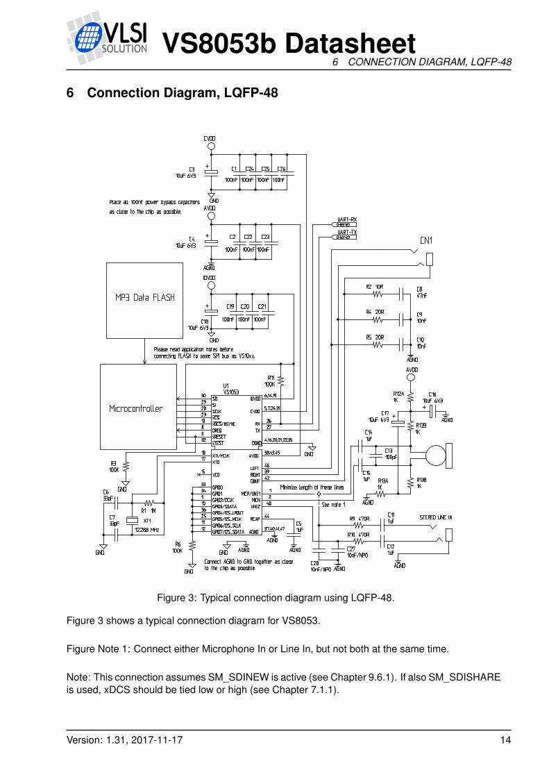
Figure 3: Typical connection diagram using LQFP-48.
Figure 3 shows a typical connection diagram for VS8053.
Figure Note 1: Connect either Microphone In or Line In, but not both at the same time.
Note: This connection assumes SM_SDINEW is active (see Chapter 9.6.1). If also SM_SDISHAREis used, xDCS should be tied low or high (see Chapter 7.1.1).
Version: 1.31, 2017-11-17 14

VS8053b Datasheet6 CONNECTION DIAGRAM, LQFP-48
The common buffer GBUF can be used for common voltage (1.23 V) for earphones. This willeliminate the need for large isolation capacitors on line outputs, and thus the audio output pinsfrom VS8053b may be connected directly to the earphone connector.
GBUF must NOT be connected to ground under any circumstances. If GBUF is not used,LEFT and RIGHT must be provided with coupling capacitors. To keep GBUF stable, you shouldalways have the resistor and capacitor even when GBUF is not used. See application notes fordetails.
Unused GPIO pins should have a pull-down resistor. Unused line and microphone inputs shouldnot be connected.
If UART is not used, RX should be connected to IOVDD and TX be unconnected.
Do not connect any external load to XTALO.
Version: 1.31, 2017-11-17 15

VS8053b Datasheet7 SPI BUSES
7 SPI Buses
The SPI Bus - which was originally used in some Motorola devices - has been used for bothVS8053b’s Serial Data Interface SDI (Chapters 7.3 and 9.4) and Serial Control Interface SCI(Chapters 7.4 and 9.5).
7.1 SPI Bus Pin Descriptions
7.1.1 VS10xx Native Modes (New Mode, recommended)
These modes are active on VS8053b when SM_SDINEW is set to 1 (default at startup). DCLKand SDATA are not used for data transfer and they can be used as general-purpose I/O pins(GPIO2 and GPIO3). BSYNC function changes to data interface chip select (XDCS).
SDI Pin SCI Pin DescriptionXDCS XCS Active low chip select input. A high level forces the serial interface into
standby mode, ending the current operation. A high level also forces serialoutput (SO) to high impedance state. If SM_SDISHARE is 1, pinXDCS is not used, but the signal is generated internally by invertingXCS.
SCK Serial clock input. The serial clock is also used internally as the masterclock for the register interface.SCK can be gated or continuous. In either case, the first rising clock edgeafter XCS has gone low marks the first bit to be written.
SI Serial input. If a chip select is active, SI is sampled on the rising CLK edge.- SO Serial output. In reads, data is shifted out on the falling SCK edge.
In writes SO is at a high impedance state.
7.1.2 VS1001 Compatibility Mode (deprecated, do not use in new designs)
This mode is active when SM_SDINEW is set to 0. In this mode, DCLK, SDATA and BSYNCare active.
SDI Pin SCI Pin Description- XCS Active low chip select input. A high level forces the serial interface into
standby mode, ending the current operation. A high level also forces serialoutput (SO) to high impedance state.
BSYNC - SDI data is synchronized with a rising edge of BSYNC.DCLK SCK Serial clock input. The serial clock is also used internally as the master
clock for the register interface.SCK can be gated or continuous. In either case, the first rising clock edgeafter XCS has gone low marks the first bit to be written.
SDATA SI Serial input. SI is sampled on the rising SCK edge, if XCS is low.- SO Serial output. In reads, data is shifted out on the falling SCK edge.
In writes SO is at a high impedance state.
Version: 1.31, 2017-11-17 16

VS8053b Datasheet7 SPI BUSES
7.2 Data Request Pin DREQ
The DREQ pin/signal is used to signal if VS8053b’s 2048-byte FIFO is capable of receivingdata. If DREQ is high, VS8053b can take at least 32 bytes of SDI data or one SCI command.DREQ is turned low when the stream buffer is too full and for the duration of an SCI command.
Because of the 32-byte safety area, the sender may send up to 32 bytes of SDI data at atime without checking the status of DREQ, making controlling VS8053b easier for low-speedmicrocontrollers.
Note: DREQ may turn low or high at any time, even during a byte transmission. Thus, DREQshould only be used to decide whether to send more bytes. A transmission that has alreadystarted doesn’t need to be aborted.
Note: In VS8053b DREQ also goes down while an SCI operation is in progress.
There are cases when you still want to send SCI commands when DREQ is low. BecauseDREQ is shared between SDI and SCI, you can not determine if an SCI command has beenexecuted if SDI is not ready to receive data. In this case you need a long enough delay afterevery SCI command to make certain none of them are missed. The SCI Registers table inChapter 9.6 gives the worst-case handling time for each SCI register write.
Note: The status of DREQ can also be read through SCI with the following code. For details onSCI registers, see Chapter 7.4.
// This example reads status of DREQ pin through the SPI/SCI register
// interface.
#define SCI_WRAMADDR 7
#define SCI_WRAM 6
while (!endOfFile)
int dreq;
WriteSciReg(SCI_WRAMADDR, 0xC012); // Send address of DREQ register
dreq = ReadSciReg(SCI_WRAM) & 1; // Read value of DREQ (in bit 0)
if (dreq)
// DREQ high: send 1-32 bytes audio data
else
// DREQ low: wait 5 milliseconds (so that VS10xx doesn't get
// continuous SCI operations)
/* while (!endOfFile) */
Version: 1.31, 2017-11-17 17

VS8053b Datasheet7 SPI BUSES
7.3 Serial Protocol for Serial Data Interface (SPI / SDI)
The serial data interface operates in slave mode so DCLK signal must be generated by anexternal circuit.
Data (SDATA signal) can be clocked in at either the rising or falling edge of DCLK (Chapter 9.6).
VS8053b assumes its data input to be byte-sychronized. SDI bytes may be transmitted eitherMSb or LSb first, depending of register SCI_MODE bit SM_SDIORD (Chapter 9.6.1).
The firmware is able to accept the maximum bitrate the SDI supports.
7.3.1 SDI in VS10xx Native Modes (New Mode, recommended)
DCLK
D7 D6 D5 D4 D3 D1D2 D0SDATA
XDCS
Figure 4: SDI in VS10xx Native Mode, single-byte transfer
In VS10xx native modes (SM_NEWMODE is 1), byte synchronization is achieved by XDCS, asshown in Figure 4. The state of XDCS may not change while a data byte transfer is in progress.XDCS does not need to be deactivated and reactivated for every byte transfer, as shown inFigure 5. However, to maintain data synchronization even if there are occasional clock glitches,it is recommended to deactivate and reactivate XDCS every now and then, for example aftereach 32 bytes of data.
Note that when sending data through SDI you have to check the Data Request Pin DREQ atleast after every 32 bytes (Chapter 7.2).
DCLK
SDATA D7 D6 D5 D4 D3 D1D2 D0 D7 D6 D5 ... D3 D1D2 D0
Byte XByte 1 Byte 2
...
XDCS
Figure 5: SDI in VS10xx Native Mode, multi-byte transfer, X ≥ 1
If SM_SDISHARE is 1, the XDCS signal is internally generated by inverting the XCS input.
Version: 1.31, 2017-11-17 18

VS8053b Datasheet7 SPI BUSES
7.3.2 SDI Timing Diagram in VS10xx Native Modes (New Mode)
SCK
SI
tXCSS tXCSHtWL tWH
tH
tSU
tXCS
xDCS
D7 D6 D5 D4 D3 D2 D1 D0
Figure 6: SDI timing diagram
Figure 6 presents SDI bus timing.
Symbol Min Max UnittXCSS 5 nstSU 0 nstH 2 CLKI cyclestWL 2 CLKI cyclestWH 2 CLKI cyclestXCSH 1 CLKI cyclestXCS 0 CLKI cycles
Note: xDCS is not required to go high between bytes, so tXCS is 0.
Note: Although the timing is derived from the internal clock CLKI, the system always starts up in1.0× mode, thus CLKI=XTALI. After you have configured a higher clock through SCI_CLOCKFand waited for DREQ to rise, you can use a higher SPI speed as well.
Version: 1.31, 2017-11-17 19

VS8053b Datasheet7 SPI BUSES
7.3.3 SDI in VS1001 Compatibility Mode (deprecated, do not use in new designs)
DCLK
D7 D6 D5 D4 D3 D1D2 D0SDATA
BSYNC
Figure 7: SDI in VS1001 Mode - one byte transfer. Do not use in new designs!
When VS8053b is running in VS1001 compatibility mode, a BSYNC signal must be generatedto ensure correct bit-alignment of the input bitstream, as shown in Figures 7 and 8.
The first DCLK sampling edge (rising or falling, depending on selected polarity), during whichthe BSYNC is high, marks the first bit of a byte (LSB, if LSB-first order is used, MSB, if MSB-firstorder is used). If BSYNC is ’1’ when the last bit is received, the receiver stays active and next8 bits are also received.
DCLK
D7 D6 D5 D4 D3 D1D2 D0 D7 D6 D5 D4 D3 D2 D1 D0SDATA
BSYNC
Figure 8: SDI in VS1001 Mode - two byte transfer. Do not use in new designs!
7.3.4 Passive SDI Mode (deprecated, do not use in new designs)
If SM_NEWMODE is 0 and SM_SDISHARE is 1, the operation is otherwise like the VS1001compatibility mode, but bits are only received while the BSYNC signal is ’1’. Rising edge ofBSYNC is still used for synchronization.
Version: 1.31, 2017-11-17 20

VS8053b Datasheet7 SPI BUSES
7.4 Serial Protocol for Serial Command Interface (SPI / SCI)
The serial bus protocol for the Serial Command Interface SCI (Chapter 9.5) consists of aninstruction byte, address byte and one 16-bit data word. Each read or write operation can reador write a single register. Data bits are read at the rising edge, so the user should update dataat the falling edge. Bytes are always send MSb first. XCS should be low for the full duration ofthe operation, but you can have pauses between bits if needed.
The operation is specified by an 8-bit instruction opcode. The supported instructions are readand write. See table below.
InstructionName Opcode OperationREAD 0b0000 0011 Read dataWRITE 0b0000 0010 Write data
Note: VS8053b sets DREQ low after each SCI operation. The duration depends on the opera-tion. It is not allowed to finish a new SCI/SDI operation before DREQ is high again.
7.4.1 SCI Read
0 1 2 3 4 5 6 7 8 9 10 11 12 13 30 3114 15 16 17
0 0 0 0 0 0 1 1 0 0 0 0
3 2 1 0
0 0 0 0 0 0 0 0 0 0 0 0 0 0 0 0
15 14 1 0
X
instruction (read) addressdata out
XCS
SCK
SI
SO
don’t care don’t care
DREQ
execution
Figure 9: SCI word read
VS8053b registers are read from using the following sequence, as shown in Figure 9. First,XCS line is pulled low to select the device. Then the READ opcode (0x3) is transmitted viathe SI line followed by an 8-bit word address. After the address has been read in, any furtherdata on SI is ignored by the chip. The 16-bit data corresponding to the received address will beshifted out onto the SO line.
XCS should be driven high after data has been shifted out.
DREQ is driven low for a short while when in a read operation by the chip. This is a very shorttime and doesn’t require special user attention.
Version: 1.31, 2017-11-17 21

VS8053b Datasheet7 SPI BUSES
7.4.2 SCI Write
0 1 2 3 4 5 6 7 8 9 10 11 12 13 30 3114 15 16 17
0 0 0 0 0 0 1 0 0 0 0
3 2 1 0 1 0
X
address
XCS
SCK
SI
15 14
data out
0 0 0 0 0 0 0 0 0 0 0 0 0 0 0 0SO 0 0 0 0 X
0
instruction (write)
DREQ
execution
Figure 10: SCI word write
VS8053b registers are written from using the following sequence, as shown in Figure 10. First,XCS line is pulled low to select the device. Then the WRITE opcode (0x2) is transmitted via theSI line followed by an 8-bit word address.
After the word has been shifted in and the last clock has been sent, XCS should be pulled highto end the WRITE sequence.
After the last bit has been sent, DREQ is driven low for the duration of the register update,marked “execution” in the figure. The time varies depending on the register and its contents(see table in Chapter 9.6 for details). If the maximum time is longer than what it takes from themicrocontroller to feed the next SCI command or SDI byte, status of DREQ must be checkedbefore finishing the next SCI/SDI operation.
7.4.3 SCI Multiple Write
0 1 2 3 4 5 6 7 8 9 10 11 12 13 14 15 16 17
0 0 0 0 0 0 1 0 0 0 0
3 2 1 0
address
XCS
SCK
SI
15 14
0 0 0 0 0 0 0 0 0 0 0 0 0 0 0 0SO 0 0
0
instruction (write)
DREQ
1 0
X
0 0 X
execution
1 0 15 14
data out 1 data out 2
0 0 0 0
execution
X
3130 32 3329
d.out n
m−2m−1
Figure 11: SCI multiple word write
VS8053b allows for the user to send multiple words to the same SCI register, which allowsfast SCI uploads, shown in Figure 11. The main difference to a single write is that instead of
Version: 1.31, 2017-11-17 22

VS8053b Datasheet7 SPI BUSES
bringing XCS up after sending the last bit of a data word, the next data word is sent immediately.After the last data word, XCS is driven high as with a single word write.
After the last bit of a word has been sent, DREQ is driven low for the duration of the registerupdate, marked “execution” in the figure. The time varies depending on the register and itscontents (see table in Chapter 9.6 for details). If the maximum time is longer than what it takesfrom the microcontroller to feed the next SCI command or SDI byte, status of DREQ must bechecked before finishing the next SCI/SDI operation.
7.4.4 SCI Timing Diagram
XCS
SCK
SI
SO
0 1 1514 16
tXCSS tXCSHtWL tWH
tH
tSU
tV
tZ
tDIS
tXCS30 31
Figure 12: SPI timing diagram
The SCI timing diagram is presented in Figure 12.
Symbol Min Max UnittXCSS 5 nstSU 0 nstH 2 CLKI cyclestZ 0 nstWL 2 CLKI cyclestWH 2 CLKI cyclestV 2 (+ 25 ns1) CLKI cyclestXCSH 1 CLKI cyclestXCS 2 CLKI cyclestDIS 10 ns
1 25 ns is when pin loaded with 100 pF capacitance. The time is shorter with lower capacitance.
Note: Although the timing is derived from the internal clock CLKI, the system always starts up in1.0× mode, thus CLKI=XTALI. After you have configured a higher clock through SCI_CLOCKFand waited for DREQ to rise, you can use a higher SPI speed as well.
Note: Because tWL + tWH + tH is 6×CLKI + 25 ns, the maximum speed for SCI reads is CLKI/7.
Version: 1.31, 2017-11-17 23

VS8053b Datasheet7 SPI BUSES
7.5 SPI Examples with SM_SDINEW and SM_SDISHARED set
7.5.1 Two SCI Writes
0 1 2 3 30 31
1 0 1 0
0 0 0 0 0 0X X
XCS
SCK
SI
2
32 33 61 62 63
SCI Write 1 SCI Write 2
DREQ
DREQ up before finishing next SCI write
Figure 13: Two SCI operations
Figure 13 shows two consecutive SCI operations. Note that xCS must be raised to inactivestate between the writes. Also DREQ must be respected as shown in the figure.
7.5.2 Two SDI Bytes
1 2 3
XCS
SCK
SI
7 6 5 4 3 1 0 7 6 5 2 1 0
X
SDI Byte 1SDI Byte 2
0 6 7 8 9 13 14 15
DREQ
Figure 14: Two SDI bytes
SDI data is synchronized with a raising edge of xCS as shown in Figure 14. However, everybyte doesn’t need separate synchronization.
Version: 1.31, 2017-11-17 24

VS8053b Datasheet7 SPI BUSES
7.5.3 SCI Operation in Middle of Two SDI Bytes
0 1
XCS
SCK
SI
7
7 6 5 1
0 0
0 7 6 5 1 0
SDI ByteSCI Operation
SDI Byte
8 9 39 40 41 46 47
X
DREQ high before end of next transfer
DREQ
Figure 15: Two SDI bytes separated by an SCI operation
Figure 15 shows how an SCI operation is embedded in between SDI operations. xCS edgesare used to synchronize both SDI and SCI. Remember to respect DREQ as shown in the figure.
Version: 1.31, 2017-11-17 25

VS8053b Datasheet8 SUPPORTED AUDIO DECODER FORMATS
8 Supported Audio Decoder Formats
ConventionsMark Description+ Format is supported? Format is supported but not thoroughly tested- Format exists but is not supported
Format doesn’t exist
8.1 Supported Ogg Vorbis Formats
Parameter Min Max UnitChannels 2Window size 64 4096 samplesSamplerate 100 48000 HzBitrate 500 kbit/sec
Only floor 1 is supported. No known current encoder uses floor 0. All one- and two-channelOgg Vorbis files should be playable with this decoder.
Version: 1.31, 2017-11-17 26

VS8053b Datasheet8 SUPPORTED AUDIO DECODER FORMATS
8.2 Supported FLAC Formats
Up to 48 kHz and 24-bit FLAC files are supported with the VS1053b Patches w/ FLAC Decoderplugin that is available at http://www.vlsi.fi/en/support/software/vs10xxpatches.html . Read theaccompanying documentation of the plugin for details.
NOTE! VS1053b Patches w/ FLAC Decoder can also be used in the VS8053b.
8.3 Supported RIFF WAV Formats
The most common RIFF WAV subformats are supported, with 1 or 2 audio channels.
Format Name Supported Comments0x01 PCM + 16 and 8 bits, any samplerate ≤ 48kHz0x02 ADPCM -0x03 IEEE_FLOAT -0x06 ALAW -0x07 MULAW -0x10 OKI_ADPCM -0x11 IMA_ADPCM + Any samplerate ≤ 48kHz0x15 DIGISTD -0x16 DIGIFIX -0x30 DOLBY_AC2 -0x31 GSM610 -0x3b ROCKWELL_ADPCM -0x3c ROCKWELL_DIGITALK -0x40 G721_ADPCM -0x41 G728_CELP -0x50 MPEG -0x55 MPEGLAYER3 -0x64 G726_ADPCM -0x65 G722_ADPCM -
Version: 1.31, 2017-11-17 27

VS8053b Datasheet9 FUNCTIONAL DESCRIPTION
9 Functional Description
9.1 Main Features
VS8053b is based on a proprietary digital signal processor, VS_DSP. It contains all the codeand data memory needed for Ogg Vorbis, WAV PCM + ADPCM audio decoding togetherwith serial interfaces, a multirate stereo audio DAC and analog output amplifiers and filters.Also PCM/ADPCM audio encoding is supported using a microphone amplifier and/or line-levelinputs and a stereo A/D converter. With software plugins the chip can also decode losslessFLAC as well as record the high-quality Ogg Vorbis format. A UART is provided for debuggingpurposes.
Version: 1.31, 2017-11-17 28

VS8053b Datasheet9 FUNCTIONAL DESCRIPTION
9.2 Data Flow of VS8053b
Volumecontrol
AudioFIFO
S.rate.conv.and DAC R
BitstreamFIFO
SDI
L
SCI_VOL
SM_ADPCM=0
2048 stereo samples
Bassenhancer
SB_AMPLITUDE=0
SB_AMPLITUDE!=0
AIADDR = 0
AIADDR != 0
UserApplication
ST_AMPLITUDE=0
ST_AMPLITUDE!=0
EarSpeaker
Treblecontrol
WAV ADPCMVorbis
Figure 16: Data flow of VS8053b.
First, depending on the audio data, and provided ADPCM encoding mode is not set, OggVorbis, PCM WAV or IMA ADPCM WAV is received and decoded from the SDI bus.
After decoding, if SCI_AIADDR is non-zero, application code is executed from the addresspointed to by that register. For more details, see Application Notes for VS10XX.
Then data may be sent to the Bass Enhancer and Treble Control depending on the SCI_BASSregister.
Next, headphone processing is performed, if the EarSpeaker spatial processing is active.
After that the data to the Audio FIFO, which holds the data until it is read by the Audio interruptand fed to the samplerate converter and DACs. The size of the audio FIFO is 2048 stereo(2×16-bit) samples, or 8 KiB.
The samplerate converter upsamples all different samplerates to XTALI/2, or 128 times thehighest usable samplerate with 18-bit precision. Volume control is performed in the upsampleddomain. New volume settings are loaded only when the upsampled signal crosses the zeropoint (or after a timeout). This zero-crossing detection almost completely removes all audiblenoise that occurs when volume is suddenly changed.
The samplerate conversion to a common samplerate removes the need for complex PLL-basedclocking schemes and allows almost unlimited sample rate accuracy with one fixed input clockfrequency. With a 12.288 MHz clock, the DA converter operates at 128 × 48 kHz, i.e. 6.144MHz, and creates a stereo in-phase analog signal. The oversampled output is low-pass filteredby an on-chip analog filter. This signal is then forwarded to the earphone amplifier.
Version: 1.31, 2017-11-17 29

VS8053b Datasheet9 FUNCTIONAL DESCRIPTION
9.3 EarSpeaker Spatial Processing
While listening to headphones the sound has a tendency to be localized inside the head. Thesound field becomes flat and lacking the sensation of dimensions. This is an unnatural, awk-ward and sometimes even disturbing situation. This phenomenon is often referred in literatureas ‘lateralization’, meaning ’in-the-head’ localization. Long-term listening to lateralized soundmay lead to listening fatigue.
All real-life sound sources are external, leaving traces to the acoustic wavefront that arrives tothe ear drums. From these traces, the auditory system of the brain is able to judge the distanceand angle of each sound source. In loudspeaker listening the sound is external and thesetraces are available. In headphone listening these traces are missing or ambiguous.
EarSpeaker processes sound to make listening via headphones more like listening to the samemusic from real loudspeakers or live music. Once EarSpeaker processing is activated, theinstruments are moved from inside to the outside of the head, making it easier to separatethe different instruments (see figure 17). The listening experience becomes more natural andpleasant, and the stereo image is sharper as the instruments are widely on front of the listenerinstead of being inside the head.
Figure 17: EarSpeaker externalized sound sources vs. normal inside-the-head sound
Note that EarSpeaker differs from any common spatial processing effects, such as echo, reverb,or bass boost. EarSpeaker accurately simulates the human auditory model and real listeningenvironment acoustics. Thus is does not change the tonal character of the music by introducingartificial effects.
EarSpeaker processing can be parameterized to a few different modes, each simulating a littledifferent type of acoustical situation, suiting different personal preferences and types of record-ing. See section 9.6.1 for how to activate different modes.
• Off: Best option when listening through loudspeakers or if the audio to be played containsbinaural preprocessing.
• minimal: Suited for listening to normal musical scores with headphones, very subtle.
Version: 1.31, 2017-11-17 30

VS8053b Datasheet9 FUNCTIONAL DESCRIPTION
• normal: Suited for listening to normal musical scores with headphones, moves soundsource further away than minimal.
• extreme: Suited for old or ’dry’ recordings, or if the audio to be played is artificial, forexample generated MIDI.
9.4 Serial Data Interface (SDI)
The serial data interface is meant for transferring compressed data for the different decoders ofVS8053b.
If the input of the decoder is invalid or it is not received fast enough, analog outputs are auto-matically muted.
Also several different tests may be activated through SDI as described in Chapter 10.
9.5 Serial Control Interface (SCI)
The serial control interface is compatible with the SPI bus specification. Data transfers arealways 16 bits. VS8053b is controlled by writing and reading the registers of the interface.
The main controls of the serial control interface are:
• control of the operation mode, clock, and builtin effects• access to status information and header data• receiving encoded data in recording mode• uploading and controlling user programs
Version: 1.31, 2017-11-17 31

VS8053b Datasheet9 FUNCTIONAL DESCRIPTION
9.6 SCI Registers
VS8053b sets DREQ low when it detects an SCI operation (this delay is 16 to 40 CLKI cyclesdepending on whether an interrupt service routine is active) and restores it when it has pro-cessed the operation. The duration depends on the operation. If DREQ is low when an SCIoperation is performed, it also stays low after SCI operation processing.
If DREQ is high before a SCI operation, do not start a new SCI/SDI operation before DREQ ishigh again. If DREQ is low before a SCI operation because the SDI can not accept more data,make certain there is enough time to complete the operation before sending another.
SCI registers, prefix SCI_Reg Type Reset Time1 Abbrev[bits] Description0x0 rw 0x40006 80 CLKI4 MODE Mode control0x1 rw 0x000C3 80 CLKI STATUS Status of VS8053b0x2 rw 0 80 CLKI BASS Built-in bass/treble control0x3 rw 0 1200 XTALI5 CLOCKF Clock freq + multiplier0x4 rw 0 100 CLKI DECODE_TIME Decode time in seconds0x5 rw 0 450 CLKI2 AUDATA Misc. audio data0x6 rw 0 100 CLKI WRAM RAM write/read0x7 rw 0 100 CLKI WRAMADDR Base address for RAM
write/read0x8 r 0 80 CLKI HDAT0 Stream header data 00x9 r 0 80 CLKI HDAT1 Stream header data 10xA rw 0 210 CLKI2 AIADDR Start address of application0xB rw 0 80 CLKI VOL Volume control0xC rw 0 80 CLKI2 AICTRL0 Application control register 00xD rw 0 80 CLKI2 AICTRL1 Application control register 10xE rw 0 80 CLKI2 AICTRL2 Application control register 20xF rw 0 80 CLKI2 AICTRL3 Application control register 3
1 This is the worst-case time that DREQ stays low after writing to this register. The user maychoose to skip the DREQ check for those register writes that take less than 100 clock cycles toexecute and use a fixed delay instead.2 In addition, the cycles spent in the user application routine must be counted.3 Firmware changes the value of this register immediately to 0x48 (analog enabled), and aftera short while to 0x40 (analog drivers enabled).4 When mode register write specifies a software reset the worst-case time is 22000 XTALIcycles.5 If the clock multiplier is changed, writing to CLOCKF register may force internal clock to runat 1.0× XTALI for a while. Thus it is not a good idea to send SCI or SDI bits while this registerupdate is in progress.6 Firmware changes the value of this register immediately to 0x4800.
Reads from all SCI registers complete in under 100 CLKI cycles, except a read from AIADDRin 200 cycles. In addition the cycles spent in the user application routine must be counted tothe read time of AIADDR, AUDATA, and AICTRL0..3.
Version: 1.31, 2017-11-17 32

VS8053b Datasheet9 FUNCTIONAL DESCRIPTION
9.6.1 SCI_MODE (RW)
SCI_MODE is used to control the operation of VS8053b and defaults to 0x4800 (SM_SDINEWset).
Bit Name Function Value Description0 SM_DIFF Differential 0 normal in-phase audio
1 left channel inverted1 SM_LAYER12 Not used in VS8053 0 no
1 yes2 SM_RESET Soft reset 0 no reset
1 reset3 SM_CANCEL Cancel decoding current file 0 no
1 yes4 SM_EARSPEAKER_LO EarSpeaker low setting 0 off
1 active5 SM_TESTS Allow SDI tests 0 not allowed
1 allowed6 SM_STREAM Stream mode 0 no
1 yes7 SM_EARSPEAKER_HI EarSpeaker high setting 0 off
1 active8 SM_DACT DCLK active edge 0 rising
1 falling9 SM_SDIORD SDI bit order 0 MSb first
1 MSb last10 SM_SDISHARE Share SPI chip select 0 no
1 yes11 SM_SDINEW VS10xx native SPI modes 0 no
1 yes12 SM_ADPCM PCM/ADPCM recording active 0 no
1 yes13 - - 0 right
1 wrong14 SM_LINE1 MIC / LINE1 selector 0 MICP
1 LINE115 SM_CLK_RANGE Input clock range 0 12..13 MHz
1 24..26 MHz
When SM_DIFF is set, the player inverts the left channel output. For a stereo input this createsvirtual surround, and for a mono input this creates a differential left/right signal.
SM_LAYER12 has no function in VS8053 because it does not support MPEG audio decoding.
Software reset is initiated by setting SM_RESET to 1. This bit is cleared automatically.
If you want to stop decoding a in the middle, set SM_CANCEL, and continue sending datahonouring DREQ. When SM_CANCEL is detected by a codec, it will stop decoding and returnto the main loop. The stream buffer content is discarded and the SM_CANCEL bit cleared.SCI_HDAT1 will also be cleared. See Chapter 10.5.2 for details.
Bits SM_EARSPEAKER_LO and SM_EARSPEAKER_HI control the EarSpeaker spatial pro-cessing. If both are 0, the processing is not active. Other combinations activate the processingand select 3 different effect levels: LO = 1, HI = 0 selects minimal, LO = 0, HI = 1 selects nor-mal, and LO = 1, HI = 1 selects extreme. EarSpeaker takes approximately 12 MIPS at 44.1 kHz
Version: 1.31, 2017-11-17 33

VS8053b Datasheet9 FUNCTIONAL DESCRIPTION
samplerate.
If SM_TESTS is set, SDI tests are allowed. For more details on SDI tests, look at Chapter 10.11.
SM_STREAM activates VS8053b’s stream mode. In this mode, data should be sent with aseven intervals as possible and preferable in blocks of less than 512 bytes, and VS8053b makesevery attempt to keep its input buffer half full by changing its playback speed up to 5%. For bestquality sound, the average speed error should be within 0.5%, the bitrate should not exceed160 kbit/s and VBR should not be used. For details, see Application Notes for VS10XX. Thismode only works with WAV files.
SM_DACT defines the active edge of data clock for SDI. When ’0’, data is read at the risingedge, when ’1’, data is read at the falling edge.
When SM_SDIORD is clear, bytes on SDI are sent MSb first. By setting SM_SDIORD, the usermay reverse the bit order for SDI, i.e. bit 0 is received first and bit 7 last. Bytes are, however,still sent in the default order. This register bit has no effect on the SCI bus.
Setting SM_SDISHARE makes SCI and SDI share the same chip select, as explained in Chap-ter 7.1, if also SM_SDINEW is set.
Setting SM_SDINEW will activate VS10xx native serial modes as described in Chapters 7.1.1 and 7.3.1.Note, that this bit is set as a default when VS8053b is started up.
By activating SM_ADPCM and SM_RESET at the same time, the user will activate IMA ADPCMrecording mode (see section 10.8).
SM_LINE_IN is used to select the left-channel input for ADPCM recording. If ’0’, differentialmicrophone input pins MICP and MICN are used; if ’1’, line-level MICP/LINEIN1 pin is used.
SM_CLK_RANGE activates a clock divider in the XTAL input. When SM_CLK_RANGE is set,the clock is divided by 2 at the input. From the chip’s point of view e.g. 24 MHz becomes12 MHz. SM_CLK_RANGE should be set as soon as possible after a chip reset.
Version: 1.31, 2017-11-17 34

VS8053b Datasheet9 FUNCTIONAL DESCRIPTION
9.6.2 SCI_STATUS (RW)
SCI_STATUS contains information on the current status of VS8053b. It also controls somelow-level things that the user does not usually have to care about.
Name Bits DescriptionSS_DO_NOT_JUMP 15 Header in decode, do not fast forward/rewindSS_SWING 14:12 Set swing to +0 dB, +0.5 dB, .., or +3.5 dBSS_VCM_OVERLOAD 11 GBUF overload indicator ’1’ = overloadSS_VCM_DISABLE 10 GBUF overload detection ’1’ = disable
9:8 reservedSS_VER 7:4 VersionSS_APDOWN2 3 Analog driver powerdownSS_APDOWN1 2 Analog internal powerdownSS_AD_CLOCK 1 AD clock select, ’0’ = 6 MHz, ’1’ = 3 MHzSS_REFERENCE_SEL 0 Reference voltage selection, ’0’ = 1.23 V, ’1’ = 1.65 V
SS_DO_NOT_JUMP is set when a WAV or Ogg Vorbis header is being decoded and jumpingto another location in the file is not allowed. If you use soft reset or cancel, clear this bit yourselfor it can be accidentally left set.
If AVDD is at least 3.3 V, SS_REFERENCE_SEL can be set to select 1.65 V reference voltageto increase the analog output swing.
SS_AD_CLOCK can be set to divide the AD modulator frequency by 2 if XTALI/2 is too much.
SS_VER is 0 for VS1001, 1 for VS1011, 2 for VS1002, 3 for VS1003, 4 for VS1053 and VS8053,5 for VS1033, 7 for VS1103, and 6 for VS1063.
SS_APDOWN2 controls analog driver powerdown. SS_APDOWN1 controls internal analogpowerdown. These bit are meant to be used by the system firmware only.
If the user wants to powerdown VS8053b with a minimum power-off transient, set SCI_VOL to0xffff, then wait for at least a few milliseconds before activating reset.
VS8053b contains GBUF protection circuit which disconnects the GBUF driver when too muchcurrent is drawn, indicating a short-circuit to ground. SS_VCM_OVERLOAD is high while theoverload is detected. SS_VCM_DISABLE can be set to disable the protection feature.
SS_SWING allows you to go above the 0 dB volume setting. Value 0 is normal mode, 1 gives+0.5 dB, and 2 gives +1.0 dB. Settings from 3 to 7 cause the DAC modulator to be overdrivenand should not be used. You can use SS_SWING with I2S to control the amount of headroom.
Note: Due to a firmware bug in the VS8053b volume calculation routine clears SS_AD_CLOCKand SS_REFERENCE_SEL bits. Writes to SCI_STATUS or SCI_VOL, and sample rate changes(if bass enhancer or treble control are active) causes the volume calculation routine to be called.See the VS1053b Patches w/ FLAC Decoder plugin for a workaround:http://www.vlsi.fi/en/support/software/vs10xxpatches.html
Version: 1.31, 2017-11-17 35

VS8053b Datasheet9 FUNCTIONAL DESCRIPTION
9.6.3 SCI_BASS (RW)
Name Bits DescriptionST_AMPLITUDE 15:12 Treble Control in 1.5 dB steps (-8..7, 0 = off)ST_FREQLIMIT 11:8 Lower limit frequency in 1000 Hz steps (1..15)SB_AMPLITUDE 7:4 Bass Enhancement in 1 dB steps (0..15, 0 = off)SB_FREQLIMIT 3:0 Lower limit frequency in 10 Hz steps (2..15)
The Bass Enhancer VSBE is a bass boosting DSP algorithm, which tries to take the most outof the users earphones without causing clipping.
VSBE is activated when SB_AMPLITUDE is non-zero. SB_AMPLITUDE should be set to theuser’s preferences, and SB_FREQLIMIT to roughly 1.5 times the lowest frequency the user’saudio system can reproduce. For example setting SCI_BASS to 0x00f6 will have 15 dB en-hancement below 60 Hz. When the bass enhancer is in use with VS1053b, the bass portion iscalculated in mono.
Note: Because VSBE tries to avoid clipping, it gives the best bass boost with dynamical musicmaterial, or when the playback volume is not set to maximum. It also does not create bass: thesource material must have some bass to begin with.
Treble Control VSTC is activated when ST_AMPLITUDE is non-zero. For example settingSCI_BASS to 0x7a00 will have 10.5 dB treble enhancement at and above 10 kHz.
Bass Enhancer uses about 2.1 MIPS and Treble Control 1.2 MIPS at 44100 Hz samplerate.Both can be on simultaneously.
In VS8053b bass and treble initialization and volume change is delayed until the next batch ofsamples are sent to the audio FIFO. Thus, unlike with earlier VS10XX chips, audio interruptscan no longer be missed when SCI_BASS or SCI_VOL is written to.
Version: 1.31, 2017-11-17 36

VS8053b Datasheet9 FUNCTIONAL DESCRIPTION
9.6.4 SCI_CLOCKF (RW)
The external clock multiplier SCI register SCI_CLOCKF, which has changed slightly sinceVS1003 and VS1033, is presented in the table below.
SCI_CLOCKF bitsName Bits DescriptionSC_MULT 15:13 Clock multiplierSC_ADD 12:11 Allowed multiplier additionSC_FREQ 10: 0 Clock frequency
SC_MULT activates the built-in clock multiplier. This will multiply XTALI to create a higher CLKI.When the multiplier is changed by more than 0.5×, the chip runs at 1.0× clock for a few hundresclock cycles. The values are as follows:
SC_MULT MASK CLKI0 0x0000 XTALI1 0x2000 XTALI×2.02 0x4000 XTALI×2.53 0x6000 XTALI×3.04 0x8000 XTALI×3.55 0xa000 XTALI×4.06 0xc000 XTALI×4.57 0xe000 XTALI×5.0
SC_ADD tells how much the decoder firmware is allowed to add to the multiplier. It has noeffect in VS8053b. Please leave it at zero.
If SC_FREQ is non-zero, it tells that the input clock XTALI is running at something else than12.288 MHz. XTALI is set in 4 kHz steps. The formula for calculating the correct value for thisregister is XTALI−8000000
4000 (XTALI is in Hz).
Note: because maximum samplerate is XTALI256 , all samplerates are not available if XTALI <
12.288 MHz.
Version: 1.31, 2017-11-17 37

VS8053b Datasheet9 FUNCTIONAL DESCRIPTION
9.6.5 SCI_DECODE_TIME (RW)
When decoding correct data, current decoded time is shown in this register in full seconds.
The user may change the value of this register. In that case the new value should be writtentwice to make absolutely certain that the change is not overwritten by the firmware. A write toSCI_DECODE_TIME also resets the byteRate calculation.
SCI_DECODE_TIME is reset at every hardware and software reset. It is no longer clearedwhen decoding of a file ends to allow the decode time to proceed automatically with loopedfiles and with seamless playback of multiple files.
With fast playback (see the playSpeed extra parameter) the decode time also counts faster.
Some codecs (Ogg Vorbis) can also indicate the absolute play position, see the positionMsec
extra parameter in section 10.10.
9.6.6 SCI_AUDATA (RW)
When decoding correct data, the current samplerate and number of channels can be foundin bits 15:1 and 0 of SCI_AUDATA, respectively. Bits 15:1 contain the samplerate divided bytwo, and bit 0 is 0 for mono data and 1 for stereo. Writing to SCI_AUDATA will change thesamplerate directly.
Example: 44100 Hz stereo data reads as 0xAC45 (44101).Example: 11025 Hz mono data reads as 0x2B10 (11024).Example: Writing 0xAC80 sets samplerate to 44160 Hz, stereo mode does not change.
To reduce digital power consumption when idle, you can write a low samplerate to SCI_AUDATA.
Note: Ogg Vorbis decoding overrides AUDATA change. If you want to fine-tune samplerate instreaming applications with Ogg Vorbis, use SCI_CLOCKF to control the playback rate insteadof AUDATA.
9.6.7 SCI_WRAM (RW)
SCI_WRAM is used to upload application programs and data to instruction and data RAMs.The start address must be initialized by writing to SCI_WRAMADDR prior to the first write/readof SCI_WRAM. As 16 bits of data can be transferred with one SCI_WRAM write/read, and theinstruction word is 32 bits long, two consecutive writes/reads are needed for each instructionword. The byte order is big-endian (i.e. most significant words first). After each full-wordwrite/read, the internal pointer is autoincremented.
Version: 1.31, 2017-11-17 38

VS8053b Datasheet9 FUNCTIONAL DESCRIPTION
9.6.8 SCI_WRAMADDR (W)
SCI_WRAMADDR is used to set the program address for following SCI_WRAM writes/reads.Use an address offset from the following table to access X, Y, I or peripheral memory.
WRAMADDR Dest. addr. Bits/ DescriptionStart. . . End Start. . . End Word0x1800. . . 0x18XX 0x1800. . . 0x18XX 16 X data RAM0x5800. . . 0x58XX 0x1800. . . 0x18XX 16 Y data RAM0x8040. . . 0x84FF 0x0040. . . 0x04FF 32 Instruction RAM0xC000. . . 0xFFFF 0xC000. . . 0xFFFF 16 I/O
Only user areas in X, Y, and instruction memory are listed above. Other areas can be accessed,but should not be written to unless otherwise specified.
9.6.9 SCI_HDAT0 and SCI_HDAT1 (R)
For WAV files, SCI_HDAT1 contains 0x7665 (“ve”). SCI_HDAT0 contains the data rate mea-sured in bytes per second for all supported RIFF WAVE formats: mono and stereo 8-bit or16-bit PCM, mono and stereo IMA ADPCM. To get the bitrate of the file, multiply the value by 8.
For Ogg Vorbis files, SCI_HDAT1 contains 0x4F67 “Og”. SCI_HDAT0 contains the averagedata rate in bytes per second. To get the bitrate of the file, multiply the value by 8.
Version: 1.31, 2017-11-17 39

VS8053b Datasheet9 FUNCTIONAL DESCRIPTION
9.6.10 SCI_AIADDR (RW)
SCI_AIADDR indicates the start address of the application code written earlier with SCI_WRAMADDRand SCI_WRAM registers. If no application code is used, this register should not be initialized,or it should be initialized to zero. For more details, see Application Notes for VS10XX.
Note: Reading AIADDR is not recommended. It can cause samplerate to be set to a very lowvalue.
9.6.11 SCI_VOL (RW)
SCI_VOL is a volume control for the player hardware. The most significant byte of the volumeregister controls the left channel volume, the low part controls the right channel volume. Thechannel volume sets the attenuation from the maximum volume level in 0.5 dB steps. Thus,maximum volume is 0x0000 and total silence is 0xFEFE.
Note, that after hardware reset the volume is set to full volume. Resetting the software doesnot reset the volume setting.
Setting SCI_VOL to 0xFFFF will activate analog powerdown mode.
Example: for a volume of -2.0 dB for the left channel and -3.5 dB for the right channel: (2.0/0.5)= 4, 3.5/0.5 = 7→ SCI_VOL = 0x0407.
Example: SCI_VOL = 0x2424→ both left and right volumes are 0x24 * -0.5 = -18.0 dB.
In VS8053b bass and treble initialization and volume change is delayed until the next batch ofsamples are sent to the audio FIFO. Thus, audio interrupts can no longer be missed during awrite to SCI_BASS or SCI_VOL.
This delays the volume setting slightly, but because the volume control is now done in the DAChardware instead of performing it to the samples going into the audio FIFO, the overall volumechange response is better than before. Also, the actual volume control has zero-cross detec-tion, which almost completely removes all audible noise that occurs when volume is suddenlychanged.
9.6.12 SCI_AICTRL[x] (RW)
SCI_AICTRL[x] registers ( x=[0 .. 3] ) can be used to access the user’s application program.
The AICTRL registers are also used with PCM/ADPCM encoding mode.
Version: 1.31, 2017-11-17 40

VS8053b Datasheet10 OPERATION
10 Operation
10.1 Clocking
VS8053b operates on a single, nominally 12.288 MHz fundamental frequency master clock.This clock can be generated by external circuitry (connected to pin XTALI) or by the internalclock crystal interface (pins XTALI and XTALO). This clock is used by the analog parts anddetermines the highest available samplerate. With 12.288 MHz clock all samplerates up to48000 Hz are available.
VS8053b can also use 24..26 MHz clocks when SM_CLK_RANGE in the SCI_MODE register isset to 1. The system clock is then divided by 2 at the clock input and the chip gets a 12..13 MHzinput clock.
10.2 Hardware Reset
When the XRESET -signal is driven low, VS8053b is reset and all the control registers andinternal states are set to the initial values. XRESET-signal is asynchronous to any externalclock. The reset mode doubles as a full-powerdown mode, where both digital and analog partsof VS8053b are in minimum power consumption stage, and where clocks are stopped. AlsoXTALO is grounded.
When XRESET is asseted, all output pins go to their default states. All input pins will go tohigh-impedance state (to input state), except SO, which is still controlled by the XCS.
After a hardware reset (or at power-up) DREQ will stay down for around 22000 clock cycles,which means an approximate 1.8 ms delay if VS8053b is run at 12.288 MHz. After this theuser should set such basic software registers as SCI_MODE, SCI_BASS, SCI_CLOCKF, andSCI_VOL before starting decoding. See section 9.6 for details.
If the input clock is 24..26 MHz, SM_CLK_RANGE should be set as soon as possible after achip reset without waiting for DREQ.
Internal clock can be multiplied with a PLL. Supported multipliers through the SCI_CLOCKFregister are 1.0 × . . . 5.0× the input clock. Reset value for Internal Clock Multiplier is 1.0×. Iftypical values are wanted, the Internal Clock Multiplier needs to be set to 3.5× after reset. Waituntil DREQ rises, then write value 0x9800 to SCI_CLOCKF (register 3). See section 9.6.4 fordetails.
10.3 Software Reset
In some cases the decoder software has to be reset. This is done by activating bit SM_RESETin register SCI_MODE (Chapter 9.6.1). Then wait for at least 2 µs, then look at DREQ. DREQ
Version: 1.31, 2017-11-17 41

VS8053b Datasheet10 OPERATION
will stay down for about 22000 clock cycles, which means an approximate 1.8 ms delay ifVS8053b is run at 12.288 MHz. After DREQ is up, you may continue playback as usual.
As opposed to all earlier VS10XX chips, it is not recommended to do a software reset betweensongs. This way the user may be sure that even files with low samplerates or bitrates are playedright to their end.
10.4 Low Power Mode
If you need to keep the system running while not decoding data, but need to lower the powerconsumption, you can use the following tricks.
• Select the 1.0× clock by writing 0x0000 to SCI_CLOCKF. This disables the PLL and savessome power.
• Write a low non-zero value, such as 0x0010 to SCI_AUDATA. This will reduce the sam-plerate and the number of audio interrupts required. Between audio interrupts the VSDSPcore will just wait for an interrupt, thus saving power.
• Turn off all audio post-processing (tone controls and EarSpeaker).
• If possible for the application, write 0xffff to SCI_VOL to disable the analog drivers.
To return from low-power mode, revert register values in reverse order.
Note: The low power mode consumes significantly more electricity than hardware reset.
10.5 Play and Decode
This is the normal operation mode of VS8053b. SDI data is decoded. Decoded samples areconverted to analog domain by the internal DAC. If no decodable data is found, SCI_HDAT0and SCI_HDAT1 are set to 0.
When there is no input for decoding, VS8053b goes into idle mode (lower power consumptionthan during decoding) and actively monitors the serial data input for valid data.
Version: 1.31, 2017-11-17 42

VS8053b Datasheet10 OPERATION
10.5.1 Playing a Whole File
This is the default playback mode.
1. Send an audio file to VS8053b.2. Read extra parameter value endFillByte (Chapter 10.10).3. Send at least 2052 bytes of endFillByte[7:0].4. Set SCI_MODE bit SM_CANCEL.5. Send at least 32 bytes of endFillByte[7:0].6. Read SCI_MODE. If SM_CANCEL is still set, go to 5. If SM_CANCEL hasn’t cleared
after sending 2048 bytes, do a software reset (this should be extremely rare).7. The song has now been successfully sent. HDAT0 and HDAT1 should now both contain
0 to indicate that no format is being decoded. Return to 1.
10.5.2 Cancelling Playback
Cancelling playback of a song is a normal operation when the user wants to jump to anothersong while doing playback.
1. Send a portion of an audio file to VS8053b.2. Set SCI_MODE bit SM_CANCEL.3. Continue sending audio file, but check SM_CANCEL after every 32 bytes of data. If it
is still set, goto 3. If SM_CANCEL doesn’t clear after 2048 bytes or one second, do asoftware reset (this should be extremely rare).
4. When SM_CANCEL has cleared, read extra parameter value endFillByte (Chapter 10.10).5. Send 2052 bytes of endFillByte[7:0].6. HDAT0 and HDAT1 should now both contain 0 to indicate that no format is being decoded.
You can now send the next audio file.
10.5.3 Fast Play
VS8053b allows fast audio playback. If your microcontroller can feed data fast enough to theVS8053b, this is the preferred way to fast forward audio.
1. Start sending an audio file to VS8053b.2. To set fast play, set extra parameter value playSpeed (Chapter 10.10).3. Continue sending audio file.4. To exit fast play mode, write 1 to playSpeed.
To estimate whether or not your microcontroller can feed enough data to VS8053b in fast playmode, see contents of extra parameter value byteRate (Chapter 10.10). Note that byteRatecontains the data speed of the file played back at nominal speed even when fast play is active.
Note: Play speed is not reset when song is changed.
Version: 1.31, 2017-11-17 43

VS8053b Datasheet10 OPERATION
10.5.4 Fast Forward and Rewind without Audio
To do fast forward and rewind you need the capability to do random access to the audio file.Unfortunately fast forward and rewind isn’t available at all times, like when file headers arebeing read.
1. Send a portion of an audio file to VS8053b.2. When random access is required, read SCI_STATUS bit SS_DO_NOT_JUMP. If that bit
is set, random access cannot be performed, so go back to 1.3. Read extra parameter value endFillByte (Chapter 10.10).4. Send at least 2048 bytes of endFillByte[7:0].5. Jump forwards or backwards in the file.6. Continue sending the file.
Note: It is recommended that playback volume is decreased by e.g. 10 dB when fast forward-ing/rewinding.
Note: Register DECODE_TIME does not take jumps into account.
10.5.5 Maintaining Correct Decode Time
When fast forward and rewind operations are performed, there is no way to maintain correctdecode time for most files. However, Ogg Vorbis files offer exact time information in the file. Touse accurate time information whenever possible, use the following algorithm:
1. Start sending an audio file to VS8053b.2. Read extra parameter value pair positionMsec (Chapter 10.10).3. If positionMsec is -1, show you estimation of decoding time using DECODE_TIME (and
your estimate of file position if you have performed fast forward / rewind operations).4. If positionMsec is not -1, use this time to show the exact position in the file.
Version: 1.31, 2017-11-17 44

VS8053b Datasheet10 OPERATION
10.6 Feeding PCM Data
VS8053b can be used as a PCM decoder by sending a WAV file header. If the length sent in theWAV header is 0xFFFFFFFF, VS8053b will stay in PCM mode indefinitely (or until SM_CANCELhas been set). 8-bit (unsigned) linear and 16-bit (signed, 2’s complement) linear audio is sup-ported in mono or stereo. A WAV header looks like this:
File Offset Field Name Size Bytes Description0 ChunkID 4 "RIFF"
4 ChunkSize 4 0xff 0xff 0xff 0xff8 Format 4 "WAVE"
12 SubChunk1ID 4 "fmt "
16 SubChunk1Size 4 0x10 0x0 0x0 0x0 1620 AudioFormat 2 0x1 0x0 Linear PCM22 NumOfChannels 2 C0 C1 1 for mono, 2 for stereo24 SampleRate 4 S0 S1 S2 S3 0x1f40 for 8 kHz28 ByteRate 4 R0 R1 R2 R3 0x3e80 for 8 kHz 16-bit mono32 BlockAlign 2 A0 A1 0x02 0x00 for mono, 0x04 0x00 for stereo 16-bit34 BitsPerSample 2 B0 B1 0x10 0x00 for 16-bit data52 SubChunk2ID 4 "data"
56 SubChunk2Size 4 0xff 0xff 0xff 0xff Data size
The rules to calculate the four variables are as follows:• S = sample rate in Hz, e.g. 44100 for 44.1 kHz.• For 8-bit data B = 8, and for 16-bit data B = 16.• For mono data C = 1, for stereo data C = 2.• A = C×B
8 .• R = S ×A.
Example: A 44100 Hz 16-bit stereo PCM header would read as follows:0000 52 49 46 46 ff ff ff ff 57 41 56 45 66 6d 74 20 |RIFF....WAVEfmt |
0100 10 00 00 00 01 00 02 00 44 ac 00 00 10 b1 02 00 |........D.......|
0200 04 00 10 00 64 61 74 61 ff ff ff ff |....data....|
10.7 Ogg Vorbis Recording
Ogg Vorbis is an open file format that allows for very high sound quality with low to mediumbitrates.
Ogg Vorbis recording is activated by loading the Ogg Vorbis Encoder Application to the 16KiB program RAM memory of the VS8053b. After activation, encoder results can be readfrom registers SCI_HDAT0 and SCI_HDAT1, much like when using PCM/ADPCM recording(Chapter 10.8).
Three profiles are provided: one for high-quality stereo recording at a bitrate of approx. 140kbit/s, and two for speech-quality mono recording at a bitrates between 15 and 30 kbit/s.
To use the Ogg Vorbis Encoder application, please load the application from VLSI Solution’sWeb page http://www.vlsi.fi/en/support/software/vs10xxapplications.html and read the accom-panying documentation.
Version: 1.31, 2017-11-17 45

VS8053b Datasheet10 OPERATION
10.8 PCM / ADPCM Recording
This chapter explains how to record a RIFF/WAV file in PCM or IMA ADPCM format. IMEADPCM is a widely supported ADPCM format and many PC audio playback programs can playit. IMA ADPCM recording gives a compression ratio of almost 4:1 compared to linear, 16-bitaudio. This makes it possible to record for example ono 8 kHz audio at 32.44 kbit/s.
VS8053 has a stereo ADC, thus also two-channel (separate AGC, if AGC enabled) and stereo(common AGC, if AGC enabled) modes are available. Mono recording mode selects either theleft or right channel. Left channel is either MIC or LINE1 depending on the SCI_MODE register.
If absolute best quality stereo PCM recording at 48 kHz is required, download and use theVS1053 WAV PCM Recorder Application plugin, available for download athttp://www.vlsi.fi/en/support/software/vs10xxapplications.html . If you use it, follow the instruc-tions of the plugin documentation instead of this datasheet.
10.8.1 Activating PCM / ADPCM Recording Mode
Register Bits DescriptionSCI_MODE 2, 12, 14 Start ADPCM mode, select MIC/LINE1SCI_AICTRL0 15..0 Sample rate 8000..48000 Hz (read at recording startup)SCI_AICTRL1 15..0 Recording gain (1024 = 1×) or 0 for automatic gain controlSCI_AICTRL2 15..0 Maximum autogain amplification (1024 = 1×, 65535 = 64×)SCI_AICTRL3 1..0 0 = joint stereo (common AGC),
1 = dual channel (separate AGC),2 = left channel,3 = right channel
2 0 = IMA ADPCM mode, 1 = LINEAR PCM mode15..3 reserved, set to 0
PCM / IMA ADPCM recording mode is activated by setting bit SM_ADPCM in SCI_MODEand loading and starting a patch code. Line input 1 is used instead of differential mic in-put if SM_LINE1 is set. Before activating ADPCM recording, user must write the right val-ues to SCI_AICTRL0 and SCI_AICTRL3. These values are only read at recording startup.SCI_AICTRL1 and SCI_AICTRL2 can be altered anytime, but it is preferable to write good initvalues before activation.
SCI_AICTRL1 controls linear recording gain. 1024 is equal to digital gain 1, 512 is equal todigital gain 0.5 and so on. If the user wants to use automatic gain control (AGC), SCI_AICTRL1should be set to 0. Typical speech applications usually are better off using AGC, as this takescare of relatively uniform speech loudness in recordings.
SCI_AICTRL2 controls the maximum AGC gain. This can be used to limit the amplification ofnoise when there is no signal. If SCI_AICTRL2 is zero, the maximum gain is initialized to 65535(64×), i.e. whole range is used.
For example:
Version: 1.31, 2017-11-17 46

VS8053b Datasheet10 OPERATION
WriteVS10xxRegister(SCI_AICTRL0, 16000U);
WriteVS10xxRegister(SCI_AICTRL1, 0);
WriteVS10xxRegister(SCI_AICTRL2, 4096U);
WriteVS10xxRegister(SCI_AICTRL3, 0);
WriteVS10xxRegister(SCI_MODE, ReadVS10xxRegister(SCI_MODE) |
SM_ADPCM | SM_LINE1);
#ifdef I_HAVE_THE_VS1053B_PATCHES_PACKAGE
/* Strongly recommended to use the VS1053b Patches package. Get it at
http://www.vlsi.fi/en/support/software/vs10xxpatches.html */
LoadVS1053PatchesPackage(); /* Loads patches and starts recording */
#else
/* If not using the VS1053b Patches package, you need to do these steps */
WriteVS10xxPatch();
#endif
selects 16 kHz, stereo mode with automatic gain control and maximum amplification of 4×.
It is strongly recommended to always run the VS1053b Patches package, available athttp://www.vlsi.fi/en/support/software/vs10xxpatches.html , when encoding. If you are not run-ning the VS1053b Patches package, you need to implement WriteVS10xxPatch() for the exam-ple above. The function must perform the following SCI writes:
Register Reg. No ValuesSCI_WRAMADDR 0x7 0x8050SCI_WRAM 0x6 0x0000,0x1790,0xf400,0x5400,0x0000,0x0a10,0xf400,0x5600,
0xb080,0x0024,0x0007,0x9257,0x3f00,0x0024,0x0030,0x0297,
0x3f00,0x0024,0x0000,0x004d,0x0014,0x958f,0x0000,0x1b4e,
0x280f,0xe100,0x0006,0x2016,0x2a00,0x17ce,0x3e12,0xb817,
0x3e14,0xf812,0x3e01,0xb811,0x0007,0x9717,0x0020,0xffd2,
0x0030,0x11d1,0x3111,0x8024,0x3704,0xc024,0x3b81,0x8024,
0x3101,0x8024,0x3b81,0x8024,0x3f04,0xc024,0x2808,0x4800,
0x36f1,0x9811,0x2814,0x9c91,0x0000,0x004d,0x2814,0x9940,
0x003f,0x0013,
SCI_AIADDR 0xa 0x0050
This small and incomplete patch is also available from VLSI Solution’s web pagehttp://www.vlsi.fi/en/support/software/vs10xxpatches.html by the name of VS1053b IMA AD-PCM Encoder Fix.
10.8.2 Reading PCM / IMA ADPCM Data
After PCM / IMA ADPCM recording has been activated, registers SCI_HDAT0 and SCI_HDAT1have new functions.
The PCM / IMA ADPCM sample buffer is 1024 16-bit words. The fill status of the buffer canbe read from SCI_HDAT1. If SCI_HDAT1 is greater than 0, you can read as many 16-bit wordsfrom SCI_HDAT0. If the data is not read fast enough, the buffer overflows and returns to emptystate.
Note: if SCI_HDAT1 ≥ 768, it may be better to wait for the buffer to overflow and clear beforereading samples. That way you may avoid buffer aliasing.
Version: 1.31, 2017-11-17 47

VS8053b Datasheet10 OPERATION
In IMA ADPCM mode each mono IMA ADPCM block is 128 words, i.e. 256 bytes, and stereoIMA ADPCM block is 256 words, i.e. 512 bytes. If you wish to interrupt reading data andpossibly continue later, please stop at the boundary. This way complete compression blocksare skipped and the encoded stream stays valid.
10.8.3 Adding a PCM RIFF Header
To make your PCM file a RIFF / WAV file, you have to add a header to the data. The followingshows a header for a mono file. Note that 2- and 4-byte values are little-endian (lowest bytefirst).
File Offset Field Name Size Bytes Description0 ChunkID 4 "RIFF"
4 ChunkSize 4 F0 F1 F2 F3 File size - 88 Format 4 "WAVE"
12 SubChunk1ID 4 "fmt "
16 SubChunk1Size 4 0x10 0x0 0x0 0x0 2020 AudioFormat 2 0x01 0x0 0x1 for PCM22 NumOfChannels 2 C0 C1 1 for mono, 2 for stereo24 SampleRate 4 R0 R1 R2 R3 0x1f40 for 8 kHz28 ByteRate 4 B0 B1 B2 B3 0x3e80 for 8 kHz mono32 BlockAlign 2 0x02 0x00 2 for mono, 4 for stereo34 BitsPerSample 2 0x10 0x00 16 bits / sample36 SubChunk3ID 4 "data"
40 SubChunk3Size 4 D0 D1 D2 D3 Data size (File Size-36)44 Samples... Audio samples
The values in the table are calculated as follows:R = Fs (see Chapter 10.8.1 to see how to calculate Fs)B = 2× Fs × C
If you know beforehand how much you are going to record, you may fill in the complete headerbefore any actual data. However, if you don’t know how much you are going to record, you haveto fill in the header size datas F and D after finishing recording.
The PCM data is read from SCI_HDAT0 and written into file as follows. The low 8 bits ofSCI_HDAT0 should be written as the first byte to a file, then the high 8 bits (little-endian order).Note that this is different from how ADPCM data is written to a file (see Chapter 10.8.4).
Below is an example of a valid header for a 44.1 kHz mono PCM file that has a final length of1798768 (0x1B7270) bytes:0000 52 49 46 46 68 72 1b 00 57 41 56 45 66 6d 74 20 |RIFFhr..WAVEfmt |
0010 10 00 00 00 01 00 01 00 80 bb 00 00 00 77 01 00 |.............w..|
0020 02 00 10 00 64 61 74 61 44 72 1b 00 |....dataDr......|
Version: 1.31, 2017-11-17 48

VS8053b Datasheet10 OPERATION
10.8.4 Adding an IMA ADPCM RIFF Header
To make your IMA ADPCM file a RIFF / WAV file, you have to add a header to the data. Thefollowing shows a header for a mono file. Note that 2- and 4-byte values are little-endian (lowestbyte first).
File Offset Field Name Size Bytes Description0 ChunkID 4 "RIFF"
4 ChunkSize 4 F0 F1 F2 F3 File size - 88 Format 4 "WAVE"
12 SubChunk1ID 4 "fmt "
16 SubChunk1Size 4 0x14 0x0 0x0 0x0 2020 AudioFormat 2 0x11 0x0 0x11 for IMA ADPCM22 NumOfChannels 2 C0 C1 1 for mono, 2 for stereo24 SampleRate 4 R0 R1 R2 R3 0x1f40 for 8 kHz28 ByteRate 4 B0 B1 B2 B3 0xfd7 for 8 kHz mono32 BlockAlign 2 0x00 0x01 256 for mono, 512 for stereo34 BitsPerSample 2 0x04 0x00 4-bit ADPCM36 ByteExtraData 2 0x02 0x00 238 ExtraData 2 0xf9 0x01 Samples per block (505)40 SubChunk2ID 4 "fact"
44 SubChunk2Size 4 0x4 0x0 0x0 0x0 448 NumOfSamples 4 S0 S1 S2 S352 SubChunk3ID 4 "data"
56 SubChunk3Size 4 D0 D1 D2 D3 Data size (File Size-60)60 Block1 256 First ADPCM block, 512 bytes for stereo
316 . . . More ADPCM data blocks
If we have n audio blocks, the values in the table are as follows:F = n× C × 256 + 52R = Fs (see Chapter 10.8.1 to see how to calculate Fs)B = Fs×C×256
505S = n× 505. D = n× C × 256
If you know beforehand how much you are going to record, you may fill in the complete headerbefore any actual data. However, if you don’t know how much you are going to record, you haveto fill in the header size datas F , S and D after finishing recording.
The 128 words (256 words for stereo) of an ADPCM block are read from SCI_HDAT0 andwritten into file as follows. The high 8 bits of SCI_HDAT0 should be written as the first byte to afile, then the low 8 bits (big-endian order). Note that this is contrary to the native byte order ofsome 16-bit microcontrollers, and you may have to take extra care to do this right. Note also,that this is different from how PCM data is written to a file (see Chapter 10.8.3).
To see if you have written the mono file in the right way check bytes 2 and 3 (the first bytecounts as byte 0) of each 256-byte block. Byte 2 should be in the range 0..88 and byte 3 shouldbe zero. For stereo you check bytes 2, 3, 6, and 7 of each 512-byte block. Bytes 2 and 6 shouldbe in the range 0..88. Bytes 3 and 7 should be zero.
Version: 1.31, 2017-11-17 49

VS8053b Datasheet10 OPERATION
Below is an example of a valid header for a 44.1 kHz stereo IMA ADPCM file that has a finallength of 10038844 (0x992E3C) bytes:0000 52 49 46 46 34 2e 99 00 57 41 56 45 66 6d 74 20 |RIFF4...WAVEfmt |
0010 14 00 00 00 11 00 02 00 44 ac 00 00 a7 ae 00 00 |........D.......|
0020 00 02 04 00 02 00 f9 01 66 61 63 74 04 00 00 00 |........fact....|
0030 14 15 97 00 64 61 74 61 00 2e 99 00 |....data....|
10.8.5 Playing ADPCM Data
In order to play back your PCM / IMA ADPCM recordings, you have to have a file with a headeras described in Chapter 10.8.3 or Chapter 10.8.4. If this is the case, all you need to do is toprovide the ADPCM file through SDI as you would with any audio file.
10.8.6 Sample Rate Considerations
VS10xx chips that support IMA ADPCM playback are capable of playing back ADPCM files withany sample rate. However, some other programs may expect IMA ADPCM files to have someexact sample rates, like 8000 or 11025 Hz. Also, some programs or systems do not supportsample rates below 8000 Hz.
If you want better quality with the expense of increased data rate, you can use higher samplerates, for example 16 kHz.
Version: 1.31, 2017-11-17 50

VS8053b Datasheet10 OPERATION
10.8.7 Record Monitoring Volume
In VS8053b writing to the SCI_VOL register during IMA ADPCM encoding does not change thevolume. You need to set a suitable volume before activating the IMA ADPCM mode, or you canuse the VS8053 hardware volume control register DAC_VOL directly.
For example:WriteVS10xxRegister(SCI_WRAMADDR, 0xc045); /*DAC_VOL*/
WriteVS10xxRegister(SCI_WRAM, 0x0101); /*-6.0 dB*/
The hardware volume control DAC_VOL (address 0xc045) allows 0.5 dB steps for both left (high8 bits) and right channel (low 8 bits). The low 4 bits of both 8-bit values set the attenuation in6 dB steps (range 0..15), the high 4 bits in 0.5 dB steps (range 0..11). For examples, see tablebelow.
dB DAC_VOL-0.0 0x0000-0.5 0xb1b1-1.0 0xa1a1-1.5 0x9191-2.0 0x8181-2.5 0x7171-3.0 0x6161-3.5 0x5151-4.0 0x4141-4.5 0x3131-5.0 0x2121-5.5 0x1111-6.0 0x0101
dB DAC_VOL-6.5 0xb2b2: :-12.0 0x0202-12.5 0xb3b3: :-18.0 0x0303-18.5 0xb4b4: :-24.0 0x0404-24.5 0xb5b5: :-30.0 0x0505-30.5 0xb6b6
dB DAC_VOL: :-36.0 0x0606-36.5 0xb7b7: :-42.0 0x0707-42.5 0xb8b8: :-48.0 0x0808-48.5 0xb9b9: :-54.0 0x0909-54.5 0xbaba: :
dB DAC_VOL-60.0 0x0a0a-60.5 0xbbbb: :-66.0 0x0b0b-66.5 0xbcbc: :-72.0 0x0c0c-72.5 0xbdbd: :-78.0 0x0d0d-78.5 0xbebe: :-84.0 0x0e0e
Version: 1.31, 2017-11-17 51

VS8053b Datasheet10 OPERATION
10.9 SPI Boot
If GPIO0 is set with a pull-up resistor to 1 at boot time, VS8053b tries to boot from external SPImemory.
SPI boot redefines the following pins:
Normal Mode SPI Boot ModeGPIO0 xCSGPIO1 CLKDREQ MOSIGPIO2 MISO
The memory has to be an SPI Bus Serial EEPROM with 16-bit or 24-bit addresses. The serialspeed used by VS8053b is 245 kHz with the nominal 12.288 MHz clock. The first three bytesin the memory have to be 0x50, 0x26, 0x48.
Version: 1.31, 2017-11-17 52

VS8053b Datasheet10 OPERATION
10.10 Extra Parameters
The following structure is in X memory at address 0x1e02 (note the different location than inVS1033) and can be used to change some extra parameters or get useful information.
#define PARAMETRIC_VERSION 0x0003
struct parametric
/* configs are not cleared between files */
u_int16 version; /*1e02 - structure version */
u_int16 config1; /*1e03 ---- ---- ppss RRRR PS mode, SBR mode, Reverb */
u_int16 playSpeed; /*1e04 0,1 = normal speed, 2 = twice, 3 = three times etc. */
u_int16 byteRate; /*1e05 average byterate */
u_int16 endFillByte; /*1e06 byte value to send after file sent */
u_int16 reserved[16]; /*1e07..15 file byte offsets */
u_int32 jumpPoints[8]; /*1e16..25 file byte offsets */
u_int16 latestJump; /*1e26 index to lastly updated jumpPoint */
u_int32 positionMsec /*1e27-28 play position, if known (WMA, Ogg Vorbis) */
s_int16 resync; /*1e29 > 0 for automatic m4a, ADIF, WMA resyncs */
union
struct
u_int32 curPacketSize;
u_int32 packetSize;
wma;
struct
u_int16 sceFoundMask; /*1e2a SCE's found since last clear */
u_int16 cpeFoundMask; /*1e2b CPE's found since last clear */
u_int16 lfeFoundMask; /*1e2c LFE's found since last clear */
u_int16 playSelect; /*1e2d 0 = first any, initialized at aac init */
s_int16 dynCompress; /*1e2e -8192=1.0, initialized at aac init */
s_int16 dynBoost; /*1e2f 8192=1.0, initialized at aac init */
u_int16 sbrAndPsStatus; /*0x1e30 1=SBR, 2=upsample, 4=PS, 8=PS active */
aac;
struct
u_int32 bytesLeft;
midi;
struct
s_int16 gain; /* 0x1e2a proposed gain offset in 0.5dB steps, default = -12 */
vorbis;
i;
;
Notice that reading two-word variables through the SCI_WRAMADDR and SCI_WRAM inter-face is not protected in any way. The variable can be updated between the read of the low andhigh parts. The problem arises when both the low and high parts change values. To determineif the value is correct, you should read the value twice and compare the results.
The following example shows what happens when bytesLeft is decreased from 0x10000 to0xffff and the update happens between low and high part reads or after high part read.
Read InvalidAddress Value0x1e2a 0x0000 change after this0x1e2b 0x00000x1e2a 0xffff0x1e2b 0x0000
Read ValidAddress Value0x1e2a 0x00000x1e2b 0x0001 change after this0x1e2a 0xffff0x1e2b 0x0000
No UpdateAddress Value0x1e2a 0x00000x1e2b 0x00010x1e2a 0x00000x1e2b 0x0001
Version: 1.31, 2017-11-17 53

VS8053b Datasheet10 OPERATION
You can see that in the invalid read the low part wraps from 0x0000 to 0xffff while the high partstays the same. In this case the second read gives a valid answer, otherwise always use thevalue of the first read. The second read is needed when it is possible that the low part wrapsaround, changing the high part, i.e. when the low part is small. bytesLeft is only decreasedby one at a time, so a reread is needed only if the low part is 0.
10.10.1 Common Parameters
These parameters are common for all codecs. Other fields are only valid when the correspond-ing codec is active. The currently active codec can be determined from SCI_HDAT1.
Parameter Address Usageversion 0x1e02 Structure version – 0x0003config1 0x1e03 Miscellaneous configurationplaySpeed 0x1e04 0,1 = normal speed, 2 = twice, 3 = three times etc.byteRate 0x1e05 average byterateendFillByte 0x1e06 byte to send after filejumpPoints[8] 0x1e16-25 Not usedlatestJump 0x1e26 Index to latest jumpPointpositionMsec 0x1e27-28 File position in milliseconds, if availableresync 0x1e29 Not used
The fuse-programmed ID is read at startup and copied into the chipID field. If not available,the value will be all zeros. The version field can be used to determine the layout of the restof the structure. The version number is changed when the structure is changed. For VS8053bthe structure version is 3.
config1 isn’t used in VS8053.
playSpeed makes it possible to fast forward songs. Decoding of the bitstream is performed,but only each playSpeed frames are played. For example by writing 4 to playSpeed will playthe song four times as fast as normal, if you are able to feed the data with that speed. Write 0or 1 to return to normal speed. SCI_DECODE_TIME will also count faster. All current codecssupport the playSpeed configuration.
byteRate contains the average bitrate in bytes per second for every code. The value is updatedonce per second and it can be used to calculate an estimate of the remaining playtime. Thisvalue is also available in SCI_HDAT0 for all codecs.
endFillByte indicates what byte value to send after file is sent before SM_CANCEL.
positionMsec is a field that gives the current play position in a file in milliseconds, regardlessof rewind and fast forward operations. The value is only available in codecs that can determinethe play position from the stream itself. Currently Ogg Vorbis provide this information. If theposition is unknown, this field contains -1.
Version: 1.31, 2017-11-17 54

VS8053b Datasheet10 OPERATION
The file size and sample size information of WAV files are ignored when resync is non-zero.The user must use SM_CANCEL or software reset to end decoding.
10.10.2 Ogg Vorbis
Parameter Address Usagegain 0x1e2a Preferred Replay Gain offset
Ogg Vorbis decoding supports Replay Gain technology. The Replay Gain technology is usedto automatically give all songs a matching volume so that the user does not need to adjust thevolume setting between songs.
If the Ogg Vorbis decoder finds a REPLAYGAIN_ALBUM_GAIN tag in the song header, the tagis parsed and the decoded gain setting is written to the gain parameter.If REPLAYGAIN_ALBUM_GAIN is not available, REPLAYGAIN_TRACK_GAIN is used.If even REPLAYGAIN_TRACK_GAIN is not available, a default of -6 dB (gain value -12) is set.
For more information about Replay Gain, see http://en.wikipedia.org/wiki/Replay_Gain andhttp://www.replaygain.org/ .
The player software can use the gain value to adjust the volume level. Negative values meanthat the volume should be decreased, positive values mean that the volume should be in-creased.
For example gain = -11 means that volume should be decreased by 5.5 dB (−11/2 = −5.5),and left and right attenuation should be increased by 11. When gain = 2 volume should beincreased by 1 dB (2/2 = 1.0), and left and right attenuation should be decreased by 2. Becausevolume setting can not go above +0 dB, the value should be saturated.
Gain Volume SCI_VOL (Volume-Gain)-11 (-5.5 dB) 0 (+0.0 dB) 0x0b0b (-5.5 dB)-11 (-5.5 dB) 3 (-1.5 dB) 0x0e0e (-7.0 dB)+2 (+1.0 dB) 0 (+0.0 dB) 0x0000 (+0.0 dB)+2 (+1.0 dB) 1 (-0.5 dB) 0x0000 (+0.0 dB)+2 (+1.0 dB) 4 (-2.0 dB) 0x0202 (-1.0 dB)
Version: 1.31, 2017-11-17 55

VS8053b Datasheet10 OPERATION
10.11 SDI Tests
There are several test modes in VS8053b, which allow the user to perform memory tests, SCIbus tests, and several different sine wave tests.
All tests, except for the New Sine and Sweep Tests, are started in a similar way: do a hardwarereset to VS8053b, then set register SM_MODE bit SM_TESTS, and then send a test commandsequence to the SDI bus. Each test is started by sending a 4-byte special command sequence,followed by 4 zeros. The sequences are described below.
10.11.1 Old Sine Test
Sine test is initialized with the 8-byte sequence 0x53 0xEF 0x6E n 0 0 0 0, where n defines thesine test to use. n is defined as follows:
n bitsName Bits DescriptionF sIdx 7:5 Samplerate indexS 4:0 Sine skip speed
F sIdx F s F sIdx F s
0 44100 Hz 4 24000 Hz1 48000 Hz 5 16000 Hz2 32000 Hz 6 11025 Hz3 22050 Hz 7 12000 Hz
The frequency of the sine to be output can now be calculated from F = F s × S128 .
Example: Sine test is activated with value 126, which is 0b01111110. Breaking n to its compo-nents, FsIdx = 0b011 = 3 and thus Fs = 22050Hz. S = 0b11110 = 30, and thus the final sinefrequency F = 22050Hz × 30
128 ≈ 5168Hz.
To exit the sine test, send the sequence 0x45 0x78 0x69 0x74 0 0 0 0.
Note: Sine test signals go through the digital volume control, so it is possible to test channelsseparately.
Version: 1.31, 2017-11-17 56

VS8053b Datasheet10 OPERATION
10.11.2 New Sine and Sweep Tests
A more frequency-accurate sine test can be started and controlled from SCI. SCI_AICTRL0 andSCI_AICTRL1 set the sine frequencies for left and right channel, respectively. These registers,volume (SCI_VOL), and samplerate (SCI_AUDATA) can be set before or during the test. Write0x4020 to SCI_AIADDR to start the test.
SCI_AICTRLn can be calculated from the desired frequency and DAC samplerate by:
SCI_AICTRLn = Fsin × 65536/Fs
The maximum value for SCI_AICTRLn is 0x8000U. For the best S/N ratio for the generatedsine, three LSb’s of the SCI_AICTRLn should be zero. The resulting frequencies Fsin can becalculated from the DAC samplerate Fs and SCI_AICTRL0 / SCI_AICTRL1 using the followingequation.
Fsin = SCI_AICTRLn× F s/65536
Sine sweep test can be started by writing 0x4022 to SCI_AIADDR.
Both these tests use the normal audio path, thus also SCI_BASS, differential output mode, andEarSpeaker settings have an effect.
10.11.3 Pin Test
Pin test is activated with the 8-byte sequence 0x50 0xED 0x6E 0x54 0 0 0 0. This test is meantfor chip production testing only.
10.11.4 SCI Test
Sci test is initialized with the 8-byte sequence 0x53 0x70 0xEE n 0 0 0 0, where n is theregister number to test. The content of the given register is read and copied to SCI_HDAT0. Ifthe register to be tested is HDAT0, the result is copied to SCI_HDAT1.
Example: if n is 0, contents of SCI register 0 (SCI_MODE) is copied to SCI_HDAT0.
Version: 1.31, 2017-11-17 57

VS8053b Datasheet10 OPERATION
10.11.5 Memory Test
Memory test mode is initialized with the 8-byte sequence 0x4D 0xEA 0x6D 0x54 0 0 0 0. Afterthis sequence, wait for 1100000 clock cycles. The result can be read from the SCI registerSCI_HDAT0, and ’one’ bits are interpreted as follows:
Bit(s) Mask Meaning15 0x8000 Test finished14:10 Unused9 0x0200 Mux test succeeded8 0x0100 Good MAC RAM7 0x0080 Good I RAM6 0x0040 Good Y RAM5 0x0020 Good X RAM4 0x0010 Good I ROM 13 0x0008 Good I ROM 22 0x0004 Good Y ROM1 0x0002 Good X ROM 10 0x0001 Good X ROM 2
0x83ff All ok
Memory tests overwrite the current contents of the RAM memories.
Version: 1.31, 2017-11-17 58

VS8053b Datasheet11 VS8053B REGISTERS
11 VS8053b Registers
11.1 Who Needs to Read This Chapter
User software is required when a user wishes to add some own functionality like DSP effectsto VS8053b.
However, most users of VS8053b don’t need to worry about writing their own code, or aboutthis chapter, including those who only download software plug-ins from VLSI Solution’s Website.
Note: Also see VS1063 Hardware Guide for more information, because the hardware is com-patible with VS1053.
11.2 The Processor Core
VS_DSP is a 16/32-bit DSP processor core that also had extensive all-purpose processor fea-tures. VLSI Solution’s free VSKIT Software Package contains all the tools and documentationneeded to write, simulate and debug Assembly Language or Extended ANSI C programs for theVS_DSP processor core. VLSI Solution also offers a full Integrated Development EnvironmentVSIDE for full debug capabilities.
Version: 1.31, 2017-11-17 59
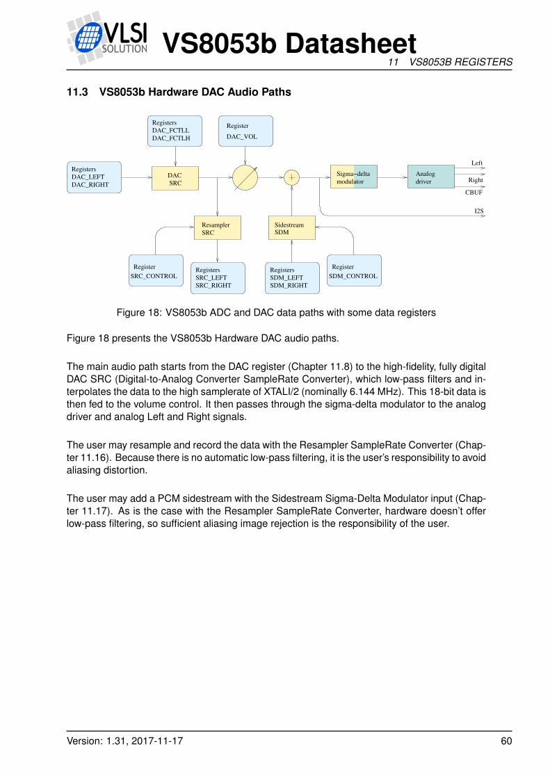
VS8053b Datasheet11 VS8053B REGISTERS
11.3 VS8053b Hardware DAC Audio Paths
Registers Registers
SRC_LEFT
SRC_RIGHT
SDM_LEFT
SDM_RIGHT
SDM
Sigma−delta
Left
Right
CBUF
I2S
SRC
Resampler Sidestream
Analog
drivermodulatorDAC
SRC
RegisterRegisters
DAC_FCTLL
DAC_FCTLH
SRC_CONTROL SDM_CONTROL
RegisterRegister
DAC_VOL
Registers
DAC_LEFT
DAC_RIGHT
Figure 18: VS8053b ADC and DAC data paths with some data registers
Figure 18 presents the VS8053b Hardware DAC audio paths.
The main audio path starts from the DAC register (Chapter 11.8) to the high-fidelity, fully digitalDAC SRC (Digital-to-Analog Converter SampleRate Converter), which low-pass filters and in-terpolates the data to the high samplerate of XTALI/2 (nominally 6.144 MHz). This 18-bit data isthen fed to the volume control. It then passes through the sigma-delta modulator to the analogdriver and analog Left and Right signals.
The user may resample and record the data with the Resampler SampleRate Converter (Chap-ter 11.16). Because there is no automatic low-pass filtering, it is the user’s responsibility to avoidaliasing distortion.
The user may add a PCM sidestream with the Sidestream Sigma-Delta Modulator input (Chap-ter 11.17). As is the case with the Resampler SampleRate Converter, hardware doesn’t offerlow-pass filtering, so sufficient aliasing image rejection is the responsibility of the user.
Version: 1.31, 2017-11-17 60

VS8053b Datasheet11 VS8053B REGISTERS
11.4 VS8053b Hardware ADC Audio Paths
Registers
Multiplexer
ADCdecimatorADC
amplifierMicrophone
MICP
LINE1
MICN
LINE2 ADC_DATA_LEFT
ADC_DATA_RIGHT
Figure 19: VS8053b ADC and DAC data paths with some data registers
Figure 18 presents the VS8053b Hardware ADC audio paths.
Analog audio may be fed up to two channels: one as a differential signal to MICN/MICP or asa one-sided signal to Line1, and the other as a one-sided signal to Line2.
If microphone input for the left channel has been selected, audio is fed through a microphoneamplifier and that signal is selected by a multiplexer.
Audio is then downsampled to one of four allowed samplerates: XTALI/64, XTALI/128, XTALI/256or XTALI/512. With the nominal 12.288 MHz crystal, these correspond to 192, 96, 48 or 24 kHzsamplerates, respectively (Chapter 11.17).
If the “3 MHz” option bit SS_AD_CLOCK in register SCI_STATUS has been set to 1, thensamplerates are divided by two, so the nominal samplerates become 96, 48, 24 and 12 kHz.
Version: 1.31, 2017-11-17 61

VS8053b Datasheet11 VS8053B REGISTERS
11.5 VS8053b Memory Map
X-memoryAddress Description0x0000..0x17ff System RAM0x1800..0x187f User RAM0x1880..0x197f Stack0x1980..0x3fff System RAM0x4000..0xbfff ROM 32k0xc000..0xc0ff Peripherals0xc100..0xffff ROM 15.75k
Y-memoryAddress Description0x0000..0x17ff System RAM0x1800..0x187f User RAM0x1880..0x197f Stack0x1980..0x3fff System RAM0x4000..0xdfff ROM 40k0xe000..0xffff System RAM
I-memoryAddress Description0x0000..0x004f System RAM0x0050..0x0fff User RAM0x1000..0x1fff -0x2000..0xffff ROM 56k
and banked0xc000..0xffff ROM4 16k
11.6 SCI Hardware Registers
SCI registers described in Chapter 9.6 can be found here between 0xC000..0xC00F. In additionto these registers, there is one in address 0xC010, called SCI_CHANGE.
SCI registers, prefix SCI_Reg Type Reset Abbrev[bits] Description
0xC010 r 0 CHANGE[5:0] Last SCI access address
SCI_CHANGE bitsName Bits DescriptionSCI_CH_WRITE 4 1 if last access was a write cycleSCI_CH_ADDR 3:0 SCI address of last access
SCI_CHANGE contains the last SCI register that has been accessed through the SCI bus, aswell as whether the access was a read or write operation.
11.7 Serial Data Interface (SDI) Registers
Whenever two bytes have been written to the SDI bus, an interrupt is generated and the datacan be read as a 16-bit big-endian value from the SDI registers. The user can control the DREQpin as if it was a general-purpose output through its own register bit.
SDI registers, prefix SER_Reg Type Reset Abbrev[bits] Description
0xC011 r 0 DATA Last received 2 bytes, big-endian0xC012 w 0 DREQ[0] DREQ pin control
Version: 1.31, 2017-11-17 62

VS8053b Datasheet11 VS8053B REGISTERS
11.8 DAC Registers
DAC registers, prefix DAC_Reg Type Reset Abbrev[bits] Description
0xC013 rw 0 FCTLL DAC frequency control, 16 LSbs0xC014 rw 0 FCTLH DAC frequency control 4MSbs, PLL control0xC015 rw 0 LEFT DAC left channel PCM value0xC016 rw 0 RIGHT DAC right channel PCM value0xC045 rw 0 VOL DAC hardware volume
The internal 20-bit register DAC_FCTL is calculated from DAC_FCTLH and DAC_FCTLL reg-isters as follows: DAC_FCTL = (DAC_FCTLH & 15)×65536 + DAC_FCTLL. Highest supportedvalue for DAC_FCTL is 0x80000.
If we define C = DAC_FCTL and X = XTALI in Hz, then the resulting samplerate fs of the asso-ciated DAC SampleRate Converter is fs = C ×X × 2−27.
Example:If C = 0x80000 and X = 12.288 MHz then fs = 524288× (12.288× 106)× 2−27 = 48000 (Hz).
Note: FCTLH bits 13:4 are used for the PLL Controller. See Chapter 11.9 for details.
DAC_VOL bitsName Bits DescriptionLEFT_FINE 15:12 Left channel gain +0.0 dB. . .+5.5 dB (0 to 11)LEFT_COARSE 11:8 Left channel attenuation in -6 dB stepsRIGHT_FINE 7:4 Right channel volume +0.0 dB. . .+5.5 dB (0 to
11)RIGHT_COARSE 3:0 Right channel attenuation in -6 dB steps
Normally DAC_VOL is handled by the firmware. DAC_VOL depends on SCI_VOL and the bassand treble settings in SCI_BASS (and optionally SS_SWING bits in SCI_STATUS).
11.9 PLL Controller
The Phase-Locked Loop (PLL) controller is used to generate clock frequencies that are higherthan the incoming (crystal-based) clock frequency. The PLL output is used by the CPU coreand some peripherals.
Configurable features include:
• VCO Enable/Disable
• Select VCO or input clock to be output clock
• Route VCO frequency to output pin
Version: 1.31, 2017-11-17 63

VS8053b Datasheet11 VS8053B REGISTERS
• Select PLL clock multiplier
At the core of the PLL controller is the VCO, a high frequency oscillator, whose oscillationfrequency is adjusted to be an integer multiple of some input frequency. As the name “Phase-Locked Loop” suggests, this is done by comparing the phase of the input frequency against thephase of a signal which is derived from the VCO output through frequency division.
If the system is stable, e.g. the comparison phase difference remains virtually zero, the PLL issaid to be “in lock”. This means that the output frequency of the VCO is stable and reliable.
The PLL is preceded by a division-by-two unit. Thus, with a nominal XTALI = 12.288 MHz, theinternal clock frequency CLKI can be adjusted with an accuracy of XTALI/2 = 6.144 MHz.
PLL control lies in DAC_FCTL bits 13:4. To see what bits 3:0 do, see Chapter 11.8.
FREQCTLH PLL bits, prefix FCH_Name Bits DescriptionPLL_LOCKED 13 0=lock failed since last test (read-only)PLL_SET_LOCK 12 1:Sets FCH_PLL_LOCKED to 1 to start lock testPLL_VCO_OUT_ENA 11 Route VCO to GPIO pin (VS1000:second cs pin)PLL_FORCE_PLL 9 1:System clock is VCO / 0:System clock is inclkPLL_DIV_INCLK 8 divide inclk by 2 (for 1.5, 2.5 or 3.5 x clk)PLL_RATE 7:4 PLL rate control
The PLL locked status can be checked by generating a high-active pulse (writing first “1” , then“0”) to FCH_PLL_SET_LOCK and reading FCH_PLL_LOCKED. FCH_PLL_LOCKED is set to“1” along with the high level of FCH_PLL_SET_LOCK and to “0” whenever the PLL falls out oflock. So if the “1” remains in FCH_PLL_LOCKED, PLL is in sync.
The PLL controller’s operation is optimized for frequencies around 12. . . 13 MHz. If you use an24. . . 26 MHz input clock, set the extra clock divider bit SM_CLK_RANGE in register SCI_MODEto 1 before activating the PLL.
It’s recommended to change the PLL rate in small steps and wait for the PLL to stabilize aftereach change. For diagnostic purposes, the PLL clock output (VCO) can be routed to an I/O pinso it can be scanned with an oscilloscope.
FCH_PLL_RATE (bits 7:4) control PLL multiplication rate. PLL multiplier is (FCH_PLL_RATE+ 1). When FCH_PLL_RATE is 0, the VCO is powered down and output clock is forced to beinput clock (same as if FCH_PLL_FORCE_PLL = 0).
Version: 1.31, 2017-11-17 64

VS8053b Datasheet11 VS8053B REGISTERS
11.10 GPIO
GPIO registers, prefix GPIO_Reg Type Reset Abbrev[bits] Description
0xC017 rw 0 DDR[9:0] Direction0xC018 r 0 IDATA[11:0] Values read from the pins0xC019 rw 0 ODATA[8:0] Values set to the pins
GPIO_DIR is used to set the direction of the GPIO pins. 1 means output. GPIO_ODATAremembers its values even if a GPIO_DIR bit is set to input.
GPIO_IDATA is used to read the pin states. In VS8053 also the SDI and SCI input pinscan be read through GPIO_IDATA: SCLK = GPIO_IDATA[8], XCS = GPIO_IDATA[9], SI =GPIO_IDATA[10], and XDCS = GPIO_IDATA[11].
In addition to data direction control for GPIO pins 0 to 7, there are two additional control bits inGPIO_DIR. GPIO_DIR[8] switches SO into software control, so that the value in GPIO_ODATA[8]is shown on SO whenever xCS is low. When GPIO_DIR[9] is set to ’1’ SCI and SDI are dis-abled. When using SCLK, xCS, SI and xDCS as general-purpose input, GPIO_DIR[9] preventstransitions in them from getting random data from SDI and/or SCI.
GPIO registers don’t generate interrupts.
Note that in VS8053b the VSDSP registers can be read and written through the SCI_WRAMADDRand SCI_WRAM registers. You can thus use the GPIO pins quite conveniently.
Version: 1.31, 2017-11-17 65

VS8053b Datasheet11 VS8053B REGISTERS
11.11 Interrupt Control
Interrupt registers, prefix INT_Reg Type Reset Abbrev[bits] Description
0xC01A rw 0 ENABLE[9:0] Interrupt enable0xC01B w 0 GLOB_DIS[-] Write to add to interrupt counter0xC01C w 0 GLOB_ENA[-] Write to subtract from interrupt counter0xC01D rw 0 COUNTER[4:0] Interrupt counter
INT_ENABLE controls the interrupts. The control bits are as follows:
INT_ENABLE bitsName Bits DescriptionINT_EN_SDM 9 Enable Sigma Delta Modulator interruptINT_EN_SRC 8 Enable SampleRate Converter interruptINT_EN_TIM1 7 Enable Timer 1 interruptINT_EN_TIM0 6 Enable Timer 0 interruptINT_EN_RX 5 Enable UART RX interruptINT_EN_TX 4 Enable UART TX interruptINT_EN_ADC 3 Enable AD modulator interruptINT_EN_SDI 2 Enable Data interruptINT_EN_SCI 1 Enable SCI interruptINT_EN_DAC 0 Enable DAC interrupt
Note: It may take up to 6 clock cycles before changing INT_ENABLE has any effect.
Writing any value to INT_GLOB_DIS adds one to the interrupt counter INT_COUNTER andeffectively disables all interrupts. It may take up to 6 clock cycles before writing to this registerhas any effect.
Writing any value to INT_GLOB_ENA subtracts one from the interrupt counter INT_COUNTER,unless it already was 0, in which case nothing happens. If, after the operation INT_COUNTERbecomes zero, interrupts selected with INT_ENABLE are restored. An interrupt routine shouldalways write to this register as the last thing it does, because interrupts automatically add oneto the interrupt counter, but subtracting it back to its initial value is the responsibility of the user.It may take up to 6 clock cycles before writing this register has any effect.
By reading INT_COUNTER the user may check if the interrupt counter is correct or not. If theregister is not 0, interrupts are disabled.
Version: 1.31, 2017-11-17 66

VS8053b Datasheet11 VS8053B REGISTERS
11.12 UART (Universal Asynchronous Receiver/Transmitter)
The RS232 UART implements a serial interface using RS232 standard 8N1 (8 data bits, noparity, 1 stop bit).
Startbit D0 D1 D2 D3 D4 D5 D6 D7
Stopbit
Figure 20: RS232 serial interface protocol
When the line is idling, it stays in logic high state. When a byte is transmitted, the transmissionbegins with a start bit (logic zero) and continues with data bits (LSB first) and ends up with astop bit (logic high). 10 bits are sent for each 8-bit byte frame.
11.12.1 UART Registers
UART registersReg Type Reset Abbrev[bits] Description
0xC028 r 0 UART_STATUS[4:0] Status0xC029 r/w 0 UART_DATA[7:0] Data0xC02A r/w 0 UART_DATAH[15:8] Data High0xC02B r/w 0 UART_DIV Divider
11.12.2 Status UART_STATUS
A read from the status register returns the transmitter and receiver states.
UART_STATUS bitsName Bits DescriptionUART_ST_FRAMEERR 4 Framing error (stop bit was 0)UART_ST_RXORUN 3 Receiver overrunUART_ST_RXFULL 2 Receiver data register fullUART_ST_TXFULL 1 Transmitter data register fullUART_ST_TXRUNNING 0 Transmitter running
UART_ST_FRAMEERR is set if the stop bit of the received byte was 0.
UART_ST_RXORUN is set if a received byte overwrites unread data when it is transferred fromthe receiver shift register to the data register, otherwise it is cleared.
UART_ST_RXFULL is set if there is unread data in the data register.
UART_ST_TXFULL is set if a write to the data register is not allowed (data register full).
UART_ST_TXRUNNING is set if the transmitter shift register is in operation.
Version: 1.31, 2017-11-17 67

VS8053b Datasheet11 VS8053B REGISTERS
11.12.3 Data UART_DATA
A read from UART_DATA returns the received byte in bits 7:0, bits 15:8 are returned as ’0’. Ifthere is no more data to be read, the receiver data register full indicator will be cleared.
A receive interrupt will be generated when a byte is moved from the receiver shift register tothe receiver data register.
A write to UART_DATA sets a byte for transmission. The data is taken from bits 7:0, otherbits in the written value are ignored. If the transmitter is idle, the byte is immediately movedto the transmitter shift register, a transmit interrupt request is generated, and transmission isstarted. If the transmitter is busy, the UART_ST_TXFULL will be set and the byte remains in thetransmitter data register until the previous byte has been sent and transmission can proceed.
11.12.4 Data High UART_DATAH
The same as UART_DATA, except that bits 15:8 are used.
11.12.5 Divider UART_DIV
UART_DIV BitsName Bits DescriptionUART_DIV_D1 15:8 Divider 1 (0..255)UART_DIV_D2 7:0 Divider 2 (6..255)
The divider is set to 0x0000 in reset. The ROM boot code must initialize it correctly dependingon the master clock frequency to get the correct bit speed. The second divider (D2) must befrom 6 to 255.
The communication speed f = fm(D1+1)×(D2)
, where fm is the master clock frequency, and f isthe TX/RX speed in bps.
Divider values for common communication speeds at 26 MHz master clock:
Version: 1.31, 2017-11-17 68

VS8053b Datasheet11 VS8053B REGISTERS
Example UART Speeds, fm = 49.152MHz
Comm. Speed [bps] UART_DIV_D1 UART_DIV_D24800 255 409600 255 20
14400 233 1519200 255 1028800 243 738400 159 857600 121 7
115200 60 7
11.12.6 UART Interrupts and Operation
Transmitter operates as follows: After an 8-bit word is written to the transmit data register it willbe transmitted instantly if the transmitter is not busy transmitting the previous byte. When thetransmission begins a TX_INTR interrupt will be sent. Status bit [1] informs the transmitter dataregister empty (or full state) and bit [0] informs the transmitter (shift register) empty state. Anew word must not be written to transmitter data register if it is not empty (bit [1] = ’0’). Thetransmitter data register will be empty as soon as it is shifted to transmitter and the transmissionis begun. It is safe to write a new word to transmitter data register every time a transmit interruptis generated.
Receiver operates as follows: It samples the RX signal line and if it detects a high to lowtransition, a start bit is found. After this it samples each 8 bit at the middle of the bit time (usinga constant timer), and fills the receiver (shift register) LSB first. Finally the data in the receiveris moved to the reveive data register, the stop bit state is checked (logic high = ok, logic low =framing error) for status bit[4], the RX_INTR interrupt is sent, status bit[2] (receive data registerfull) is set, and status bit[2] old state is copied to bit[3] (receive data overrun). After that thereceiver returns to idle state to wait for a new start bit. Status bit[2] is zeroed when the receiverdata register is read.
RS232 communication speed is set using two clock dividers. The base clock is the processormaster clock. Bits 15-8 in these registers are for first divider and bits 7-0 for second divider. RXsample frequency is the clock frequency that is input for the second divider.
Version: 1.31, 2017-11-17 69

VS8053b Datasheet11 VS8053B REGISTERS
11.13 Timers
There are two 32-bit timers that can be initialized and enabled independently of each other. Ifenabled, a timer initializes to its start value, written by a processor, and starts decrementingevery clock cycle. When the value goes past zero, an interrupt is sent, and the timer initializesto the value in its start value register, and continues downcounting. A timer stays in that loopas long as it is enabled.
A timer has a 32-bit timer register for down counting and a 32-bit TIMER1_LH register forholding the timer start value written by the processor. Timers have also a 2-bit TIMER_ENAregister. Each timer is enabled (1) or disabled (0) by a corresponding bit of the enable register.
11.13.1 Timer Registers
Timer registers, prefix TIMER_Reg Type Reset Abbrev Description
0xC030 r/w 0 CONFIG[7:0] Timer configuration0xC031 r/w 0 ENABLE[1:0] Timer enable0xC034 r/w 0 T0L Timer0 startvalue - LSBs0xC035 r/w 0 T0H Timer0 startvalue - MSBs0xC036 r/w 0 T0CNTL Timer0 counter - LSBs0xC037 r/w 0 T0CNTH Timer0 counter - MSBs0xC038 r/w 0 T1L Timer1 startvalue - LSBs0xC039 r/w 0 T1H Timer1 startvalue - MSBs0xC03A r/w 0 T1CNTL Timer1 counter - LSBs0xC03B r/w 0 T1CNTH Timer1 counter - MSBs
11.13.2 Configuration TIMER_CONFIG
TIMER_CONFIG BitsName Bits DescriptionTIMER_CF_CLKDIV 7:0 Master clock divider
TIMER_CF_CLKDIV is the master clock divider for all timer clocks. The generated internalclock frequency fi = fm
c+1 , where fm is the master clock frequency and c is TIMER_CF_CLKDIV.Example: With a 12 MHz master clock, TIMER_CF_DIV=3 divides the master clock by 4, andthe output/sampling clock would thus be fi = 12MHz
3+1 = 3MHz.
Version: 1.31, 2017-11-17 70
VS8053b Datasheet11 VS8053B REGISTERS
11.13.3 Configuration TIMER_ENABLE
TIMER_ENABLE BitsName Bits DescriptionTIMER_EN_T1 1 Enable timer 1TIMER_EN_T0 0 Enable timer 0
11.13.4 Timer X Startvalue TIMER_Tx[L/H]
The 32-bit start value TIMER_Tx[L/H] sets the initial counter value when the timer is reset. Thetimer interrupt frequency ft = fi
c+1 where fi is the master clock obtained with the clock divider(see Chapter 11.13.2 and c is TIMER_Tx[L/H].
Example: With a 12 MHz master clock and with TIMER_CF_CLKDIV=3, the master clock fi =3MHz. If TIMER_TH=0, TIMER_TL=99, then the timer interrupt frequency ft = 3MHz
99+1 =30kHz.
11.13.5 Timer X Counter TIMER_TxCNT[L/H]
TIMER_TxCNT[L/H] contains the current counter values. By reading this register pair, the usermay get knowledge of how long it will take before the next timer interrupt. Also, by writing tothis register, a one-shot different length timer interrupt delay may be realized.
11.13.6 Timer Interrupts
Each timer has its own interrupt, which is asserted when the timer counter underflows.
Version: 1.31, 2017-11-17 71
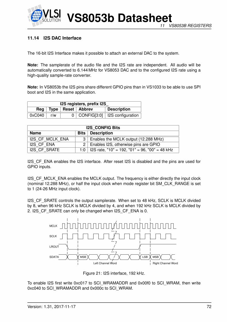
VS8053b Datasheet11 VS8053B REGISTERS
11.14 I2S DAC Interface
The 16-bit I2S Interface makes it possible to attach an external DAC to the system.
Note: The samplerate of the audio file and the I2S rate are independent. All audio will beautomatically converted to 6.144 MHz for VS8053 DAC and to the configured I2S rate using ahigh-quality sample-rate converter.
Note: In VS8053b the I2S pins share different GPIO pins than in VS1033 to be able to use SPIboot and I2S in the same application.
I2S registers, prefix I2S_Reg Type Reset Abbrev Description
0xC040 r/w 0 CONFIG[3:0] I2S configuration
I2S_CONFIG BitsName Bits DescriptionI2S_CF_MCLK_ENA 3 Enables the MCLK output (12.288 MHz)I2S_CF_ENA 2 Enables I2S, otherwise pins are GPIOI2S_CF_SRATE 1:0 I2S rate, "10" = 192, "01" = 96, "00" = 48 kHz
I2S_CF_ENA enables the I2S interface. After reset I2S is disabled and the pins are used forGPIO inputs.
I2S_CF_MCLK_ENA enables the MCLK output. The frequency is either directly the input clock(nominal 12.288 MHz), or half the input clock when mode register bit SM_CLK_RANGE is setto 1 (24-26 MHz input clock).
I2S_CF_SRATE controls the output samplerate. When set to 48 kHz, SCLK is MCLK dividedby 8, when 96 kHz SCLK is MCLK divided by 4, and when 192 kHz SCLK is MCLK divided by2. I2S_CF_SRATE can only be changed when I2S_CF_ENA is 0.
MCLK
SDATA
SCLK
LROUT
MSB LSB MSB
Left Channel Word Right Channel Word
Figure 21: I2S interface, 192 kHz.
To enable I2S first write 0xc017 to SCI_WRAMADDR and 0x00f0 to SCI_WRAM, then write0xc040 to SCI_WRAMADDR and 0x000c to SCI_WRAM.
Version: 1.31, 2017-11-17 72

VS8053b Datasheet11 VS8053B REGISTERS
11.15 Analog-to-Digital Converter (ADC)
ADC modulator registers control Analog-to-Digital conversions of VS8053b.
ADC Decimator registers, prefix ADC_Reg Type Reset Abbrev[bits] Description
0xC042 rw 0 CONTROL[4:0] ADC control0xC043 r 0 DATA_LEFT ADC left channel data0xC044 r 0 DATA_RIGHT ADC right channel data
ADC_CONTROL controls the ADC and its associated decimator unit.
ADC_CONTROL BitsName Bits DescriptionADC_MODU2_PD 4 Right channel powerdownADC_MODU1_PD 3 Left channel powerdownADC_DECIM_FACTOR 2:1 ADC Decimator factor:
- 3 = downsample to XTALI/512 (nominal 24 kHz)- 2 = downsample to XTALI/256 (nominal 48 kHz)- 1 = downsample to XTALI/128 (nominal 96 kHz)- 0 = downsample to XTALI/64 (nominal 192 kHz)
ADC_ENABLE 0 Set to activate ADC converter and decimator
Note: Setting bit SS_AD_CLOCK in register SCI_STATUS will halve the operation speed of theA/D unit, and thus halve the resulting samplerate.
Each time a new (stereo) sample has been generated, an ADC interrupt is generated.
Version: 1.31, 2017-11-17 73

VS8053b Datasheet11 VS8053B REGISTERS
11.16 Resampler SampleRate Converter (SRC)
The resampler SRC makes it possible to catch audio from the DAC path.
Note: hardware makes no attempts at low-pass filtering data. If the SRC samplerate is lowerthan the DAC samplerate, aliasing may and will occur.
Resampler SRC registers, prefix SRC_Reg Type Reset Abbrev[bits] Description
0xC046 rw 0 CONTROL[12:0] SRC control0xC047 r 0 DATA_LEFT SRC left channel data0xC048 r 0 DATA_RIGHT SRC right channel data
SRC_CONTROL BitsName Bits DescriptionSRC_ENABLE 12 Set to enable SRCSRC_DIV 11:0 Set samplerate to XTALI/2/(SRC_DIV+1)
Each time a new (stereo) sample has been generated, an SRC interrupt is generated.
Version: 1.31, 2017-11-17 74

VS8053b Datasheet11 VS8053B REGISTERS
11.17 Sidestream Sigma-Delta Modulator (SDM)
The Sidestream Sigma-Delta Modulator makes it possible to insert a digital side stream on topof existing audio.
Note: The SDM provides a direct, low-delay side channel to the Sigma-Delta DACs of VS10xx.It makes no attempts at low-pass filtering data. Thus there will be practically no image rejection.If using low samplerates, this may cause audible aliasing distortion.
Sidestream SDM registers, prefix SDM_Reg Type Reset Abbrev[bits] Description
0xC049 rw 0 CONTROL[12:0] SDM control0xC04A rw 0 DATA_LEFT SDM left channel data0xC04B rw 0 DATA_RIGHT SDM right channel data
SDM_CONTROL BitsName Bits DescriptionSDM_ENABLE 12 Set to enable SDMSDM_DIV 11:0 Set samplerate to XTALI/2/(SDM_DIV+1)
Each time a new (stereo) sample is needed, an SDM interrupt is generated.
Version: 1.31, 2017-11-17 75

VS8053b Datasheet12 VERSION CHANGES
12 Version Changes
This chapter describes the lastest and most important changes done to VS8053b
12.1 Differences Between VS1053b and VS8053b, 2010-04-30
VS8053b firmware uses laser fuse bits to disable MP3, WMA, AAC and Midi decoders. Other-wise the functionality and performance for VS1053b and VS8053b is exactly the same.
12.2 Changes Between VS1033c and VS1053a/b Firmware, 2007-03-08
Completely new or major changes:
• I2S pins are now in GPIO4-GPIO7 and do not overlap with SPI boot pins.
• No software reset required between files when used correctly.
• Ogg Vorbis decoding added. Non-fatal ogg or vorbis decode errors cause automaticresync. This allows easy rewind and fast forward. Decoding ends if the "last frame" flagis reached or SM_CANCEL is set.
• HE-AAC v2 Level 3 decoding added. It is possible to disable PS and SBR processing andcontrol the upsampling modes through parametric_x.control1.
• Like the WMA decoder, the AAC decoder uses the clock adder (see SCI_CLOCKF) if itneeds more clock to decode the file. HE-AAC features are dropped one by one, if the filecan not be decoded correctly even with the highest allowed clock. Parametric stereo isthe first feature to be dropped, then downsampled mode is used, and as the final resortSpectral Band Replication is disabled. Features are automatically restored for the nextfile.
• Completely new volume control with zero-cross detection prevents pops when volume ischanged.
• Audio FIFO underrun detection (with slow fade to zero) instead of looping the audio buffercontent.
• Average bitrate calculation (byteRate) for all codecs.
• All codecs support fast play mode with selectable speeds for the best-quality fast forwardoperation. Fast play also advances DECODE_TIME faster.
• WMA and Ogg Vorbis provide an absolute decode position in milliseconds.
• When SM_CANCEL is detected, the firmware also discards the stream buffer contents.
• Bit SCIST_DO_NOT_JUMP in SCI_STATUS is ’1’ when jumps in the file should not bedone: during header processing.
• IMA ADPCM encode now supports stereo encoding and selectable samplerate.
Other changes or additions:
Version: 1.31, 2017-11-17 76
VS8053b Datasheet12 VERSION CHANGES
• Delayed volume and bass/treble control calculation reduces the time the correspondingSCI operations take. This delayed handling and the new volume control hardware pre-vents audio samples from being missed during volume change.
• SCI_DECODE_TIME only cleared at hardware and software reset to allow files to beplayed back-to-back or looped.
• Read and write to YRAM at 0xe000..0xffff added to SCI_WRAMADDR/SCI_WRAM.
• The resync parameter (parametric_x.resync) is set to 32767 after reset to allow inifiniteresynchronization attempts (or until SM_CANCEL is set). Old operation can be restoredby writing 0 to resync after reset.
• WMA,AAC: more robust resync.
• WMA,AAC: If resync is performed, broadcast mode is automatically activated. The broad-cast mode disables file size checking, and decoding continues until SM_CANCEL is setor reset is performed.
• Treble control fixed (volume change could cause bad artefacts).
• MPEG Layer I mono fixed.
• MPEG Layer II half-rate decoding fixed (frame size was calculated wrong).
• MPEG Layer II accuracy problem fixed, invalid grouped values set to 0.
• WAV parser now skips unknown RIFF chunks.
• IMA ADPCM: Maximum blocksize is now 4096 bytes (4088 samples stereo, 8184 mono).Thus, now also plays 44100Hz stereo.
• Rt-midi: starts if in reset GPIO0=’0’, GPIO1=’1’, GPIO2&3 give earSpeaker setup.
• NewSinTest() and NewSinSweep() added (AIADDR = 0x4020/0x4022) AICTRL0 and AIC-TRL1 set sin frequency for left/right.
• Clears memory before SPI boot and not in InitHardware().
Known quirks, bugs, or features in VS1053b:
• Setting volume clears SS_REFERENCE_SEL and SS_AD_CLOCK bits. See Chap-ter 9.6.2.
• Software reset clears GPIO_DDR, also affects I2S pins.
• Ogg Vorbis occasionally overflows in windowing causing a small glitch to audio. Patchavailable (VS1053b Patches w/ FLAC Decoder plugin athttp://www.vlsi.fi/en/support/software/vs10xxpatches.html).
• IMA ADPCM encoding requires short patch to start. Patch available in Chapter 10.8.1.
• There are also fixes for some other issues, we recommend you use the latest version oftheVS1053b Patches w/ FLAC Decoder package fromhttp://www.vlsi.fi/en/support/software/vs10xxpatches.html.
Version: 1.31, 2017-11-17 77

VS8053b Datasheet13 LATEST DOCUMENT VERSION CHANGES
13 Latest Document Version Changes
This chapter describes the latest and most important changes to this document.
Version 1.31, 2017-11-17
• Split table in Chapter 4.3, Analog Characteristics, into two.
• Improved imafix in Chapter 10.8.1.
Version 1.30, 2016-12-21
• Updated numbers in Chapter 4, Characteristics & Specifications, according to re-qualificationresults.
• Added mention of 8N1 format to Chapter 11.12, UART (Universal Asynchronous Re-ceiver/Transmitter).
Version 1.22, 2014-12-19
• Added mention of RIFF 8-bit and 16-bit data signedness to Chapter 10.6, Feeding PCMData.
• Updated telephone number in Chapter 14, Contact Information.
Version 1.21, 2014-08-13
• Clarified how Ogg Vorbis set Replay Gain parameters in Chapter 10.10.2, Ogg Vorbis.
• Explained that Bass Enhancer handles the bass part of the audio signal in mono in Chap-ter 9.6.3, SCI_BASS.
• Added GPIO_DDR[9:8] and GPIO_ODATA[8] explanation to Chapter 11.10, GPIO.
• Moved value from tV(min) to tV(max) in Chapter 7.4.4, SPI Timing Diagram.
• Chapter 10.8, PCM / ADPCM Recording, has been updated to better explain how torecord using the VS1053b Patches package.
• Clarified byte endianness when reading PCM or ADPCM audio data in Chapter 10.8.3,Adding a PCM RIFF Header, and Chapter 10.8.4, Adding an IMA ADPCM RIFF Header.
Version: 1.31, 2017-11-17 78

VS8053b Datasheet14 CONTACT INFORMATION
14 Contact Information
VLSI Solution OyEntrance G, 2nd floor
Hermiankatu 8FI-33720 Tampere
FINLAND
URL: http://www.vlsi.fi/Phone: +358-50-462-3200
Commercial e-mail: [email protected]
For technical support or suggestions regarding this document, please participate athttp://www.vsdsp-forum.com/
For confidential technical discussions, [email protected]
Version: 1.31, 2017-11-17 79