Embed Size (px)
Citation preview
1
1.1 INTRODUCTION OF ELECTRONIC PACKAGE INTEGRATION
The rapid growth and convergence of digital computers and wireless communication have been driving semiconductor technology to con-tinue its evolution following Moore ’ s law in today ’ s nanometer regime. Future electronic systems require higher bandwidth with lower power consumption to handle the massive amount of data, especially for large memory systems, high - defi nition displays, and high - performance microprocessors. Electronic packaging is one of the key technologies to realize a wider bus architecture with high bandwidth operating at higher frequencies. Various packages have been developed toward a higher density structure. In particular, a three - dimensional ( 3D ) integra-tion based on through - silicon via ( TSV ) [1] arrays technology provides a potential solution to reduce the size and to increase the performance of the systems. Furthermore, nano - interconnects to replace the Cu - based interconnects provides a promising solution for long - term application.
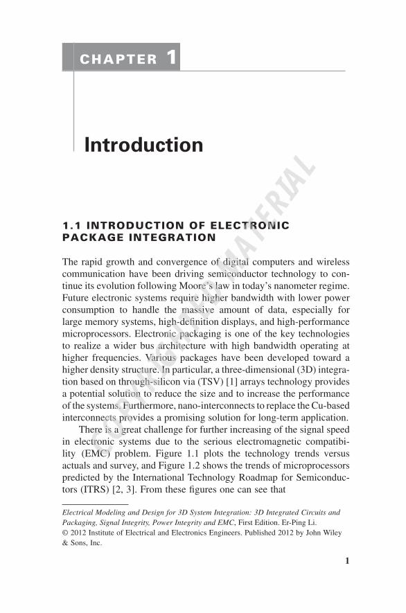
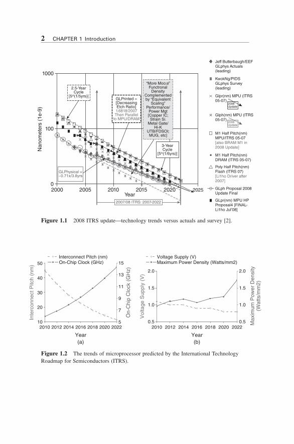
There is a great challenge for further increasing of the signal speed in electronic systems due to the serious electromagnetic compatibi-lity ( EMC ) problem. Figure 1.1 plots the technology trends versus actuals and survey, and Figure 1.2 shows the trends of microprocessors predicted by the International Technology Roadmap for Semiconduc-tors ( ITRS ) [2, 3] . From these fi gures one can see that
CHAPTER 1
Introduction
Electrical Modeling and Design for 3D System Integration: 3D Integrated Circuits and Packaging, Signal Integrity, Power Integrity and EMC, First Edition. Er-Ping Li. © 2012 Institute of Electrical and Electronics Engineers. Published 2012 by John Wiley & Sons, Inc.
COPYRIG
HTED M
ATERIAL
2 CHAPTER 1 Introduction
Figure 1.1 2008 ITRS update — technology trends versus actuals and survey [2] .
Jeff Butterbaugh/EEFGLphys Actuals(leading)
KwokNg/PIDSGLphys Survey(leading)
Glpr(nm) MPU (ITRS05-07)
2008Update
Glph(nm) MPU (ITRS05-07)
M1 Half Pitch(nm)MPU/ITRS 05-07[also BRAM M1 in2008 Update]
Poly Half Pitch(nm)Flash (ITRS 07)[Li1ho Driver after2007]
M1 Half Pitch(nm)DRAM (ITRS 05-07)
GLph Proposal 2008Update Final
2008Update
GLpr(nm) MPU HPProposal4 [FINAL-Li1ho Jul’08]
2007/08 ITRS: 2007-2022
1000
100
Nanom
ete
rs (
1e-9
)
02000 2005 2010 2015
Year2020 2025
GLPhysical =~0.71x/3.8yrs
2.5-YearCycle
[5^(1/5yrs)]
“More Moo;e”Functronal
DensityComplementedby “Equivalent
Scaling”Performance/
Power Mgt[Copper IC;Strain Si.
Metal Gate/Hi-K
UTB/FDSOI;MUG, etc]
GLPrinted =[DecreasingEtch Ratio]1.6818/2007Then Parallel
to MPU/DRAM
3-YearCycle
[5^(1/6yrs)]
Figure 1.2 The trends of microprocessor predicted by the International Technology Roadmap for Semiconductors (ITRS).
2010 2012 2014 2016 2018 2020 2022 2010 2012 2014 2016 2018 2020 202210
20
30
40
50
Interconnect Pitch (nm) Voltage Supply (V)Maximum Power Density (Watts/mm2)
Year Year
Inte
rconnect P
itch (
nm
)
5
7
9
11
13
15
0.5
1.0
1.5
2.0
Voltage S
upply
(V
)
0.5
1.0
1.5
2.0
(a) (b)
On-Chip Clock (GHz)
On-C
hip
Clo
ck (
GH
z)
Maxim
um
Pow
er
Density
(Watts/m
m2)
1.1 Introduction of Electronic Package Integration 3
• Interconnect pitch will continue to decrease to 11.3 nanometer, while the on - chip clock frequency will be increased to 14.3 GHz by 2022. Due to the reduction of the feature size and pitch, more and more circuits are integrated into one electronic package, such as the system in package ( SIP ) and the 3D integration. This results in a complex and high - density environment inside the electronic systems. At the same time, with the ever - increasing clock frequency (also its high - frequency harmonics), the physical size of the small electronic package becomes electrically large, and so the electromagnetic wave propagation inside such a small structure must be considered.
• Until 2011, the voltage supply of the microprocessor is continu-ally reduced with an increased power density. The electromag-netic noise will be pronounced due to the increased power density, which then makes the decreased voltage supply unstable. To design a high - speed and stable electronic system, we need better understand the electromagnetic interactions and the EMC issues inside the electronic package.
The EMC researches related to the high - speed circuit systems have a long history, which can be classifi ed into different levels according to the size of the interested objects, which includes the system level, printed circuit board ( PCB ) level, electronic package level, and com-ponent level. The increasing clock frequency makes the size of tiny structures on the chip be comparable with the wavelength of interest. The fl uctuation of electromagnetic wave cannot be ignored any more. Therefore, we must accurately model the electromagnetic wave behav-ior for all scales of the high - speed circuit systems. In the near future, the nanoscale integrated circuits (ICs) will be characterized by using the electric and magnetic fi elds instead of the conventional voltage and current . EM in micro - E is becoming a hot topic in both academic com-munity and industrial applications.
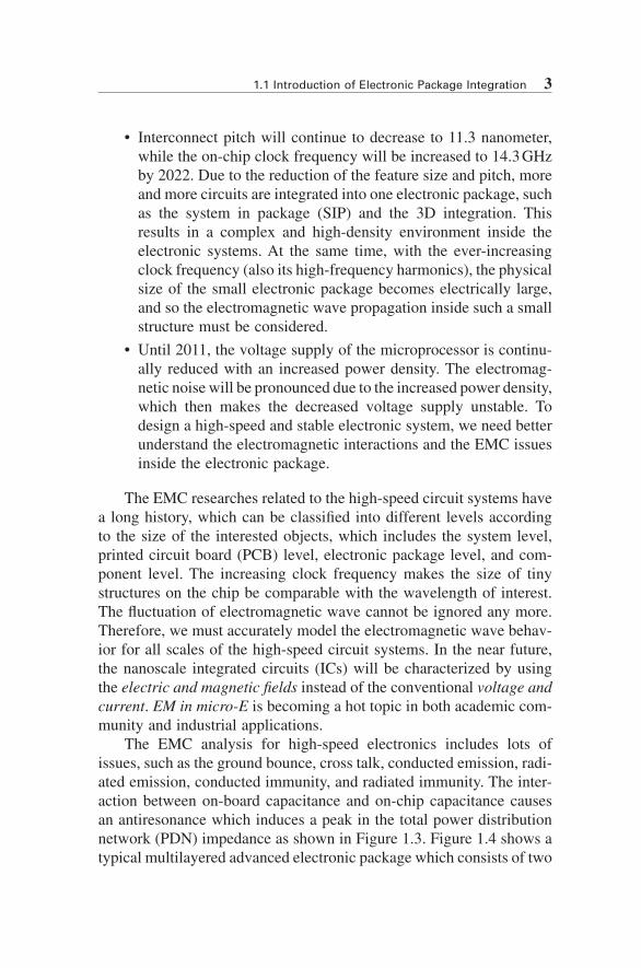
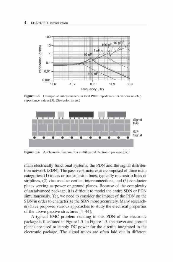
The EMC analysis for high - speed electronics includes lots of issues, such as the ground bounce, cross talk, conducted emission, radi-ated emission, conducted immunity, and radiated immunity. The inter-action between on - board capacitance and on - chip capacitance causes an antiresonance which induces a peak in the total power distribution network (PDN) impedance as shown in Figure 1.3 . Figure 1.4 shows a typical multilayered advanced electronic package which consists of two
4 CHAPTER 1 Introduction
main electrically functional systems: the PDN and the signal distribu-tion network ( SDN ). The passive structures are composed of three main categories: (1) traces or transmission lines, typically microstrip lines or striplines, (2) vias used as vertical interconnections, and (3) conductor plates serving as power or ground planes. Because of the complexity of an advanced package, it is diffi cult to model the entire SDN or PDN simultaneously. Yet, we need to consider the impact of the PDN on the SDN in order to characterize the SDN more accurately. Many research-ers have proposed various approaches to study the electrical properties of the above passive structures [4 – 44] .
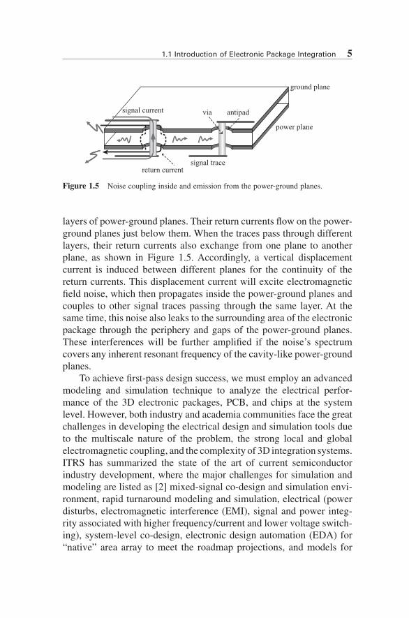
A typical EMC problem residing in this PDN of the electronic package is illustrated in Figure 1.5 . In Figure 1.5 , the power and ground planes are used to supply DC power for the circuits integrated in the electronic package. The signal traces are often laid out in different
Figure 1.3 Example of antiresonances in total PDN impedances for various on - chip capacitance values [3] . (See color insert.)
1E6 1E7 1E8 1E9 8E90.001
100 nF
10 nF1 nF
100 pF10 pF
100
10
1
0.1
0.01Impe
danc
e (o
hms)
Frequency (Hz)
Figure 1.4 A schematic diagram of a multilayered electronic package [37] .
SignalP/G
G/PSignal
1.1 Introduction of Electronic Package Integration 5
layers of power - ground planes. Their return currents fl ow on the power - ground planes just below them. When the traces pass through different layers, their return currents also exchange from one plane to another plane, as shown in Figure 1.5 . Accordingly, a vertical displacement current is induced between different planes for the continuity of the return currents. This displacement current will excite electromagnetic fi eld noise, which then propagates inside the power - ground planes and couples to other signal traces passing through the same layer. At the same time, this noise also leaks to the surrounding area of the electronic package through the periphery and gaps of the power - ground planes. These interferences will be further amplifi ed if the noise ’ s spectrum covers any inherent resonant frequency of the cavity - like power - ground planes.
To achieve fi rst - pass design success, we must employ an advanced modeling and simulation technique to analyze the electrical perfor-mance of the 3D electronic packages, PCB, and chips at the system level. However, both industry and academia communities face the great challenges in developing the electrical design and simulation tools due to the multiscale nature of the problem, the strong local and global electromagnetic coupling, and the complexity of 3D integration systems. ITRS has summarized the state of the art of current semiconductor industry development, where the major challenges for simulation and modeling are listed as [2] mixed - signal co - design and simulation envi-ronment, rapid turnaround modeling and simulation, electrical (power disturbs, electromagnetic interference (EMI), signal and power integ-rity associated with higher frequency/current and lower voltage switch-ing), system - level co - design, electronic design automation ( EDA ) for “ native ” area array to meet the roadmap projections, and models for
Figure 1.5 Noise coupling inside and emission from the power - ground planes.
signal trace
ground plane
power plane
via antipadsignal current
return current
6 CHAPTER 1 Introduction
reliability prediction. Therefore, advanced modeling techniques, which stand up to the challenges imposed by the complexity of nanoscale silicon chips and their interconnections including 3D ICs, 3D packag-ing, and PCB [45 – 47] , are in great demand.
1.2 REVIEW OF MODELING TECHNOLOGIES
Modeling of transmission lines has a long history and is well docu-mented in many textbooks [4] . So in the following, we will mainly review the modeling of vias and power - ground planes for electronic packaging and PCBs. Such modeling methods can be roughly classifi ed into three categories: (1) lumped circuit approaches, (2) full - wave approaches, and (3) hybrid circuit coupled full - wave approaches.
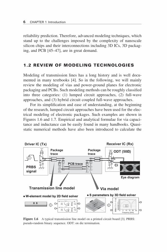
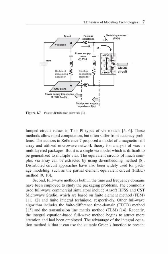
For its simplifi cation and ease of understanding, at the beginning of the research, lumped circuit approaches have been used for the elec-trical modeling of electronic packages. Such examples are shown in Figures 1.6 and 1.7 . Empirical and analytical formulae for via capaci-tance and inductance can be easily found in many handbooks. Quasi - static numerical methods have also been introduced to calculate the
Figure 1.6 A typical transmission line model on a printed circuit board [3] . PRBS: pseudo - random binary sequence. ODT: on die termination.
PCB trace
R CL G
R CL G
S dd11
S dd21
R CL G
R CL G –350 5 10 15 20 25
–30–25–20–15–10
–50
Frequency [GHz]
Sdd11
Sdd21
PCB trace
Package
trace
Driver IC (Tx)
ODT (50Ω)
Receiver IC (Rx)
Eye diagram
PRBS
signal
Ci
Package
trace
S parameters by 3D field solverS parameters by 3D field solverW-element model by 2D field solver W-element model by 2D field solver
Transmission line model Via model
R CL
R CL
G
G
1.2 Review of Modeling Technologies 7
lumped circuit values in T or PI types of via models [5, 6] . These methods allow rapid computation, but often suffer from accuracy prob-lems. The authors in Reference 7 proposed a model of a magnetic - frill array and utilized microwave network theory for analysis of vias in multilayered packages. But it is a single via model which is diffi cult to be generalized to multiple vias. The equivalent circuits of much com-plex via array can be extracted by using de - embedding method [8] . Distributed circuit approaches have also been widely used for pack-age modeling, such as the partial element equivalent circuit ( PEEC ) method [9, 10] .
Second, full - wave methods both in the time and frequency domains have been employed to study the packaging problems. The commonly used full - wave commercial simulators include Ansoft HFSS and CST Microwave Studio, which are based on fi nite element method (FEM) [11, 12] and fi nite integral technique, respectively. Other full - wave algorithm includes the fi nite - difference time - domain (FDTD) method [13] and the transmission line matrix method ( TLM ) [14] . Recently, the integral equation - based full - wave method begins to attract more attention and had been employed. The advantage of the integral equa-tion method is that it can use the suitable Green ’ s function to present
Figure 1.7 Power distribution network [3] .
Package
inductance
CMOS
circuit
Board
Power supply
noise
v(t),V(w)
Vddplane
GND plane
On-board
decoupling
capacitor
On-chip
decoupling
capacitor
VRM
Switching current
i(t),l(w)
p-MOS
n-MOS
Power supply impedance
of PCB:Zpcb(w)
Total power supply
impedance Z(w)

8 CHAPTER 1 Introduction
the effect of the complex environment, so that the unknowns are only placed on discontinuities inside the PDN. This can give an effi cient simulation. According to the different Green ’ s functions used, the inte-gral equation methods can be classifi ed into (a) two - dimensional (2D) integral equations, including 2D mode method [15] and image method for rectangular power and ground planes, and 2D transverse magnetic ( TM ) integral equation for arbitrarily shaped power and ground planes [16 – 18] ; (b) 3D integral equations, including 3D cavity mode method for rectangular power and ground planes [19] and parallel plate mode method for arbitrarily shaped power and ground planes [20, 21] . For most real applications the parallel plates have regular shapes, such as rectangles, circles, or triangles, a closed form of the Green ’ s functions can be formulated which results in an impedance formula in terms of the summation of infi nite number of resonant modes [22 – 24] . This 2D integral equation method is sometimes called the cavity resonator method. Segmentation techniques may be applied to extend the cavity resonator method for parallel plates with irregular shapes.
These full - wave methods are versatile and able to solve a wide range of problems, but at the expense of large memory usage and long CPU time, especially for those 3D full - wave methods. Although the overall size of the electronic packages is small enough to apply these full - wave methods, the high aspect ratio of the power and ground planes and the tiny structures, such as the signal traces and narrow slots, result in a huge number of meshing. This makes these full - wave methods very expensive in terms of computing time and memory requirement.
Third, to avoid the computational cost of these full - wave methods and the geometrical limitations of the analytical methods, a more effi -cient approach is to combine both methods together, so that we can benefi t from both analytic and numerical techniques. The coupled circuit - fi eld approaches are also widely used to model the electronic packages in order to leverage the advantages of both circuit and full - wave approaches. An important approach under this category is rooted in the theory of modal decomposition and the salient features of elec-tronic packages. The transmission lines and power - ground planes in an electronic package convey different modes, that is, transmission line modes and parallel plate modes. Modal decomposition can be used to decouple these two modes, which are then solved independently. These two modes are fi nally recombined to refl ect the original problem. The
1.2 Review of Modeling Technologies 9
coupling between the transmission line mode and the parallel - plate mode often occurs due to the vias. The current fl owing in the via excites the parallel - plate mode fi eld, while the transmission line experiences the loading effect of the power - ground plane in the presence of the via.
The complete modal decomposition and recombination approach has been demonstrated by several researchers. Current or voltage con-trolled sources are used to link these two modes. A general modal recombination approach was presented in Reference 26 for coupled striplines and nonideal power - ground planes, while the parallel - plate mode associated with the power - ground planes has been studied by many researchers. 2D full - wave methods have been extensively employed in the literature to model the power - ground planes. The 2D integral equation method is also called the contour integral method and has been used in Reference 16 to study general parallel - plate structures with arbitrary shapes. Another 2D approach, called the 2D FDTD, has also been used to model parallel plates [27] . Discretization of the metal plates by the fi nite - difference method was interpreted as a 2D distrib-uted LC circuit, and a rigorous derivation is given in Reference [27] . The 2D distributed RLCG (resistance, inductance, capacitance, and conductance) circuit network, which is widely used in the literature to represent the power and ground planes, can be considered as an exten-sion of the LC network derived from the fi nite - difference method. Instead of using Simulation Program with Integrated Circuit Emphasis (SPICE) - like solvers to simulate the large equivalent circuit network of power - ground planes, the latency insertion method is proposed in Reference 28 to perform fast transient simulation of large RLC net-works. Moreover, a transmission matrix method reported in Reference 29 divides the 2D distributed RLCG circuit network into many inter-dependent blocks, and each block is formulated as a transmission ( ABCD ) matrix. Cascading those transmission matrices produces a fast way to obtain the desired impedance of the power - ground plane. A multilayered fi nite - difference method ( MFDM ) was recently proposed in Reference 26 . The 2D fi nite element method ( 2D FEM ) is also used to simulate power - ground planes [30] and had been integrated into the commercial software Ansoft SIWave. In addition, the radial transmis-sion line theory has been applied to derive an admittance matrix to account for the effect of the parallel plates [31] . However, image theory [32] is needed to model the refl ection from the edges of fi nite - sized substrates. Image theory is elegant for modeling the boundary with a
10 CHAPTER 1 Introduction
regular shape but is cumbersome for modeling arbitrary shapes of the edges of PCBs or packages. In the model decomposition and recom-bination approach, a single via can be represented by a PI type of equivalent circuit. The capacitance and inductance in the PI circuit are usually computed by analytical formulae or quasi - static solvers. Recently, an elegant analytical formula was derived for the via barrel - plate capacitance [6] .
1.3 ORGANIZATION OF THE BOOK
This book is organized in six chapters. Chapter 1 provides an overview of the state - of - art of electrical modeling and simulation techniques for electrical packaging systems. Chapter 2 focuses on the macromodeling technique widely used in the electrical and electromagnetic modeling and simulation of complex interconnects in 3D integrated systems. Macromodels are generated by employing the vector fi tting ( VF ) method to perform rational - function approximation of scattering or admittance network parameters of high - speed complex interconnects and passive circuits. Subsequently, the macromodel can be synthesized as an equivalent circuit, which is compatible with the SPICE circuit simulator and can be combined with other external linear or nonlinear circuits to perform signal and power integrity analysis or other electri-cal performance analysis of electronic systems. The stability, causality, and passivity assessment and enforcement of the macromodel are also discussed in detail. Finally, numerical examples of macromodeling are presented and discussed.
In Chapter 3 , the semianalytical scattering matrix method ( SMM ) based on the N - body scattering theory is presented for modeling of 3D electronic package and multilayered PCBs with multiple vias. Using the modal expansion of fi elds in a parallel - plate waveguide, the formula derivation of the SMM is presented in detail. In the conventional SMM, the power - ground planes are assumed to be infi nitely large so they cannot capture the resonant behavior of the real - world packages. In particular, the SMM method has been extended to solve the fi nite domain of power - ground planes in coupling with a novel boundary modeling method proposed by the author ’ s group. This method has demonstrated its unique features which is capable to effi ciently handle the complex real - world 3D package integration and PCB structures.
References 11
In Chapter 4 , 2D and 3D integral equation methods are employed for the analysis of PDN in 3D package integration. The 2D integral equation method provides a comprehensive way for one to quickly extract the equivalent circuits of the PDN, and then substitute them into a SPICE - like simulator to perform the signal and power integrity analy-sis. The 3D integral equation method provides a more accurate solution for both the emission and susceptibility issues of the PDN. Both of the 2D and 3D integral equation methods are optimized by making a full use of the structural features of the PDN.
Chapter 5 is based on the physical - based algorithm to extract the equivalent circuit of the complex PDN in 3D integrated systems and PCBs. An intrinsic via circuit model is fi rst derived through rigorous electromagnetic analysis for an irregular plate pair with multiple vias in a PCB. The derivation of the intrinsic via circuit model naturally leads to a new impedance defi nition of plate pair or power - bus, which is expressed in terms of cylindrical waves. The new plate pair imped-ance has clear physical meaning and makes possible signal/power integrity co - simulations. Numerical and measurement examples have indicated that while the new impedance gives almost the same results to the conventional one in a plate pair with few vias, it can correctly predict the resonant frequency shift in the case of a plate pair with a large amount of vias.
Chapter 6 presents a compact wideband equivalent - circuit model for electrical modeling of TSVs and addresses the metal - oxide - semi-conductor ( MOS ) capacitance effects of TSVs.
REFERENCES
[1] P. Garrou , C. Bower , and P. Ramm , Handbook of 3D Integration , Wiley - VCH Verlag GmbH & Co. , Weinheim , 2008 .
[2] International Technology Roadmap for Semiconductors (ITRS) , http://www.itrs.net/ .
[3] E. - P. Li , X. C. Wei , A. C. Cangellaris , E. X. Liu , Y. J. Zhang , M. D ’ Amore , J. Kim , and T. Sudo , Progress review of electromagnetic compatibility analysis technologies for packages, PCB and novel interconnects , IEEE Trans. Electro-magn. Compat. , vol. 52 , no. 2 , pp. 248 – 265 , 2010 .
[4] C. Paul , Analysis of Multiconductor Transmission Lines , 2nd. ed. , Wiley , Hoboken, NJ , 2007 .
[5] P. A. Kok and D. D. Zutter , Prediction of the excess capacitance of a via - hole through a multilayered board including the effect of connecting microstrips or

12 CHAPTER 1 Introduction
striplines , IEEE Trans. Microw. Theory Tech. , vol. 42 , no. 12 , pp. 2270 – 2276 , 1994 .
[6] Q. Gu , Y. E. Yang , and M. A. Tassoudji , Modeling and analysis of vias in multilayered integrated circuits , IEEE Trans. Microw. Theory Tech. , vol. 41 , no. 2 , pp. 206 – 214 , 1993 .
[7] Y. J. Zhang , J. Fan , G. Selli , M. Cocchini , and D. P. Francesco , Analytical evaluation of via - plate capacitance for multilayer packages or PCBs , IEEE Trans. Microw. Theory Tech. , vol. 56 , no. 9 , pp. 2118 – 2128 , 2008 .
[8] X. C. Wei and E. P. Li , Integral - equation equivalent - circuit method for modeling of noise coupling in multilayered power distribution networks , IEEE Trans. Microw. Theory Tech. , vol. 58 , no. 3 , pp. 559 – 565 , 2010 .
[9] A. E. Ruehli , Equivalent circuit models for three - dimensional multiconductor systems , IEEE Trans. Microw. Theory Tech. , vol. 22 , pp. 216 – 221 , 1974 .
[10] A. E. Ruehli , G. Antonini , J. Esch , J. Ekman , A. Mayo , and A. Orlandi , Non - orthogonal PEEC formulation for time and frequency domain EM and circuit modeling , IEEE Trans. Electromagn. Compat. , vol. 45 , no. 2 , pp. 167 – 176 , 2003 .
[11] J. G. Yook , N. I. Dib , and L. P. B. Ratehi , Characterization of high frequency interconnects using fi nite difference time domain and fi nite element methods , IEEE Trans. Microw. Theory Tech. , vol. 42 , no. 9 , pp. 1727 – 1736 , 1994 .
[12] J. M. Jin , The Finite Element Method in Electromagnetics , John Wiley & Sons , New York , 2002 .
[13] S. Maeda , T. Kashiwa , and I. Fukai , Full wave analysis of propagation charac-teristics of a through hole using the fi nite - difference time - domain method , IEEE Trans. Microw. Theory Tech. , vol. 39 , no. 12 , pp. 2154 – 2159 , 1991 .
[14] P. B. Johns , A symmetrical condensed node for the TLM method , IEEE Trans. Microw. Theory Tech. , vol. 35 , no. 4 , pp. 370 – 377 , 1987 .
[15] T. Okoshi , Planar Circuits for Microwaves and Lightwave , Springer - Verlag , Munich, Germany , 1984 .
[16] X. C. Wei , E. P. Li , E. X. Liu , and X. Cui , Effi cient modeling of re - routed return currents in multilayered power - ground planes by using integral equation , IEEE Trans. Electromagn. Compat. , vol. 50 , no. 3 , pp. 740 – 743 , 2008 .
[17] X. C. Wei , E. P. Li , E. X. Liu , and R. Vahldieck , Effi cient simulation of power distribution network by using integral equation and modal decoupling technology , IEEE Trans. Microw. Theory Tech. , vol. 56 , no. 10 , pp. 2277 – 2285 , 2008 .
[18] M. Stumpf and M. Leone , Effi cient 2 - D integral equation approach for the analysis of power bus structures with arbitrary shape , IEEE Trans. Electromagn. Compat. , vol. 51 , no. 1 , pp. 38 – 45 , 2009 .
[19] X. C. Wei , E. P. Li , E. X. Liu , E. K. Chua , Z. Z. Oo , and R. Vahldieck , Emis-sion and susceptibility modeling of fi nite - size power - ground planes using a hybrid integral equation method , IEEE Trans. Adv. Packag. , vol. 31 , no. 3 , pp. 536 – 543 , 2008 .
[20] X. C. Wei , G. P. Zou , E. P. Li , and X. Cui , Extraction of equivalent network of arbitrarily shaped power - ground planes with narrow slots using a novel integral equation method , IEEE Trans. Microw. Theory Tech. , vol. 58 , no. 11 , pp. 2850 – 2855 , 2010 .
References 13
[21] M. R. Abdul - Gaffoor , H. K. Smith , A. A. Kishk , and A. W. A. G. A. W. Glisson , Simple and effi cient full - wave modeling of electromagnetic coupling in realistic RF multilayer PCB layouts , IEEE Trans. Microw. Theory Tech. , vol. 50 , no. 6 , pp. 1445 – 1457 , 2002 .
[22] C. Wang , J. Mao , G. Selli , S. Luan , L. Zhang , J. Fan , D. J. Pommerenke , R. E. Dubroff , and J. L. Drewniak , An effi cient approach for power delivery network design with closed - form expressions for parasitic interconnect induc-tances , IEEE Trans. Adv. Packag. , vol. 29 , no. 2 , pp. 320 – 334 , 2006 .
[23] J. Kim , Y. Jeong , J. Kim , J. Lee , C. Ryu , J. Shim , M. Shin , and J. Kim , Modeling and measurement of interlevel electromagnetic coupling and fringing effect in a hierarchical power distribution network using segmentation method with resonant cavity method , IEEE Trans. Adv. Packag. , vol. 31 , no. 3 , pp. 544 – 557 , 2008 .
[24] R. L. Chen , J. Chen , T. H. Hubing , and W. M. Shi , Analytical model for the rectangular power - ground structure including radiation loss , IEEE Trans. Elec-tromagn. Compat. , vol. 47 , pp. 10 – 16 , 2005 .
[25] A. E. Ruehli and A. C. Cangellaris , Progress in the methodologies for the electrical modeling of interconnects and electronic packages , Proc. IEEE , vol. 89 , pp. 740 – 771 , 2001 .
[26] A. E. Engin , W. John , G. Sommer , W. Mathis , and H. Reichl , Modeling of striplines between a power and a ground plane , IEEE Trans. Adv. Packag , vol. 29 , no. 3 , pp. 415 – 426 , 2006 .
[27] W. K. Gwarek , Analysis of an arbitrarily shaped planar circuit: A time - domain approach , IEEE Trans. Microw. Theory Tech. , vol. 33 , no. 10 , pp. 1067 – 1072 , 1985 .
[28] J. E. Schutt - Aine , Latency insertion method (LIM) for the fast transient simula-tion of large networks , IEEE Trans. Circuits Syst. I , vol. 48 , no. 1 , pp. 81 – 89 , 2001 .
[29] J. H. Kim and M. Swaminathan , Modeling of irregular shaped power distribu-tion planes using transmission matrix method , IEEE Trans. Adv. Packag. , vol. 24 , no. 3 , pp. 334 – 346 , 2001 .
[30] J. E. Bracken , S. Polstyanko , I. Bardi , A. Mathis , and Z. J. Cendes , Analysis of system - level electromagnetic interference from electronic packages and boards , in Proc. 14th Elect. Performance Electron. Packag. Conf. , 2005 , pp. 183 – 186 .
[31] R. Abhari , G. V. Eleftheriades , and E. van Deventer - Perkins , Physics - based CAD models for the analysis of vias in parallel - plate environments , IEEE Trans. Microw. Theory Tech. , vol. 49 , no. 10 , pp. 1697 – 1707 , 2001 .
[32] R. Ito , R. W. Jackson , and T. Hongsmatip , Modeling of interconnections and isolation within a multilayered ball grid array package , IEEE Trans. Microw. Theory Tech. , vol. 47 , no. 9 , pp. 1819 – 1825 , 1999 .
[33] L. Tsang , H. Chen , C. C. Huang , and V. Jandhyala , Modeling of multiple scattering among vias in planar waveguides using Foldy - Lax equations , Microw. Opt. Technol. Lett. , vol. 31 , pp. 201 – 208 , 2001 .
[34] L. Tsang and D. Miller , Coupling of vias in electronic packaging and printed circuit board structures with fi nite ground plane , IEEE Trans. Adv. Packag. , vol. 26 , pp. 375 – 384 , 2003 .

14 CHAPTER 1 Introduction
[35] C. C. Huang , K. L. Lai , L. Tsang , X. X. Gu , and C. J. Ong , Transmission and scattering on interconnects with via structures , Microw. Opt. Technol. Lett. , vol. 46 , pp. 446 – 452 , 2005 .
[36] C. J. Ong , D. Miller , L. Tsang , B. Wu , and C. C. Huang , Application of the Foldy - Lax multiple scattering method to the analysis of vias in ball grid arrays and interior layers of printed circuit boards , Microw. Opt. Technol. Lett. , vol. 2007 , pp. 225 – 231 , 2007 .
[37] Z. Z. Oo , E. X. Liu , E. P. Li , X. C. Wei , Y. Zhang , M. Tan , L. W. Li , and R. Vahldieck , A semi - analytical approach for system - level electrical modeling of electronic packages with large number of vias , IEEE Trans. Adv. Packag. , vol. 31 , no. 2 , pp. 267 – 274 , 2008 .
[38] E. X. Liu , E. P. Li , Z. Z. Oo , X. Wei , Y. Zhang , and R. Vahldieck , Novel methods for modeling of multiple vias in multilayered parallel - plate structures , IEEE Trans. Microw. Theory Tech. , vol. 57 , no. 7 , pp. 1724 – 1733 , 2009 .
[39] Z. Z. Oo , E. P. Li , X. C. Wei , E. X. Liu , Y. J. Zhang , and L. W. Li , Hybridization of the scattering matrix method and modal decomposition for analysis of signal traces in a power distribution network , IEEE Trans. Electromagn. Compat. , vol. 51 , no. 3 , pp. 784 – 791 , 2009 .
[40] C. Schuster , Y. Kwark , G. Selli , and P. Muthana , Developing a “ physical ” model for vias , in Proc. IEC DesignCon Conf. , Santa Clara, CA, February 6 – 9, 2006 , pp. 1 – 24 .
[41] G. Selli , C. Schuster , Y. H. Kwark , M. B. Ritter , and J. L. Drewniak , Developing a physical via model for vias — Part II: Coupled and ground return vias , in Proc. IEC DesignCon Conf. , Santa Clara, CA, January 29 – February 1, 2007 , pp. 1 – 22 .
[42] G. - T. Lei , R. W. Techentin , P. R. Hayes , D. J. Schwab , and B. K. Gilbert , Wave model solution to the ground/power plane noise problem , IEEE Trans. Instrum. Meas. , vol. 44 , no. 2 , pp. 300 – 303 , 1995 .
[43] Y. J. Zhang and J. Fan , An intrinsic via circuit model for multiple vias in an irregular plate pair through rigorous electromagnetic analysis , IEEE Trans. Microw. Theory Tech. , vol. 58 , no. 8 , pp. 2251 – 2265 , 2010 .
[44] Y. J. Zhang , Z. Z. Oo , X. C. Wei , E. X. Liu , E. P. Li , and J. Fan , Systematic microwave network analysis for multilayer printed circuit boards with vias and decoupling capacitors , IEEE Trans. Electromagn. Compat. , vol. 52 , no. 2 , pp. 401 – 409 , 2010 .
[45] Y. Xie , J. Cong , and S. Sapatnekar , Three - Dimensional Integrated Circuit Design , Springer , New York , 2010 .
[46] Y. Deng and W. P. Maly , 3 - Dimensional VLSI: A 2.5 Dimensional Integrated Scheme , Springer , New York , 2010 .
[47] S. H. Hall and H. L. Heck , Advanced Signal Integrity for High - Speed Digital Design , John Wiley & Sons , New Jersey , 2009 , pp. 274 – 279 .
[48] S. McMorrow and C. Heard , The impact of PCB laminate weave on the electri-cal performance of differential signaling at multi - gigabit data rates , DesignCon , 2005 .
[49] T. Bandyopadhyay , R. Chatterjee , D. Chung , M. Swaminathan , and R. Tummala , Electrical modeling of annular and co - axial TSVs considering MOS
References 15
capacitance effects , in IEEE 18th Conference on Electrical Performance of Elec-tronic Packaging and Systems , Portland, OR, October 2009 , pp. 117 – 120 .
[50] J. Kim , E. Song , J. Cho , J. S. Pak , H. Lee , K. Park , and J. Kim , Through silicon via equalizer , in IEEE 18th Conference on Electrical Performance of Electronic Packaging and Systems , Portland, OR, October 2009 , pp. 13 – 16 .
[51] R. Schmitt , X. Huang , L. Yang , and C. Yuan , System level power integrity analysis and correlation for multi - gigabit designs , DesignCon, 5 - WA2, 2004 .
[52] N. Hirano , M. Miura , Y. Hiruta , and T. Sudo , Characterization and reduction of simultaneous switching noise for multilayer package , in Proceedings of 44th ECTC , 1994 , pp. 949 – 956 .
[53] T. Sudo , Characterization of simultaneous switching noise and electromagnetic radiation associated with chip and package properties , IEICE Trans. Electron. , vol. J89 - C , no. 7 , pp. 429 – 439 , 2006 .
[54] M. Swaminathan , J. Kim , I. Novak , and J. Libous , Power distribution networks for system - on - package: Status and challenges , IEEE Trans. Adv. Packag. , vol. 27 , pp. 286 – 300 , 2004 .
[55] J. Qin , O. M. Ramahi , and V. Granatstein , Novel planer electromagnetic bandgap structures for wideband noise suppression and EMI reduction in high speed circuits , IEEE Trans. Electromagn. Compat. , vol. 49 , no. 3 , pp. 661 – 669 , 2007 .
[56] T. - K. Wang , T. - W. Han , and T. - L. Wu , A novel power/ground layer using arti-fi cial substrate EBG for simultaneously switching noise suppression , IEEE Trans. Microw. Theory Tech. , vol. 56 , no. 5 , pp. 1164 – 1171 , 2008 .
[57] M. Swaminathan and A. Ege Engin , Power Integrity Modeling and Design for Semiconductors and Systems , Prentice Hall , Englewood Cliffs, NJ , 2007 , pp. 415 – 445 .
![Combline Filter Tuning with Ansoft HFSS - dl.edatop.comdl.edatop.com/mte/ansoft/edatop.com_reed[1].pdf · 1 Combline Filter Tuning with Ansoft HFSS Presented by Jim Reed of Optimal](https://img.pdfslide.net/doc/110x75/5a703c537f8b9a93538bcc03/combline-filter-tuning-with-ansoft-hfss-dledatopcomdledatopcommteansoftedatopcomreed1pdfpdf.jpg)