Embed Size (px)
Citation preview
W66BM6NB / W66CM2NQ
2Gb / 4Gb LPDDR4X
Publication Release Date: Sep. 18, 2019
Revision: A01-003
- 1 -
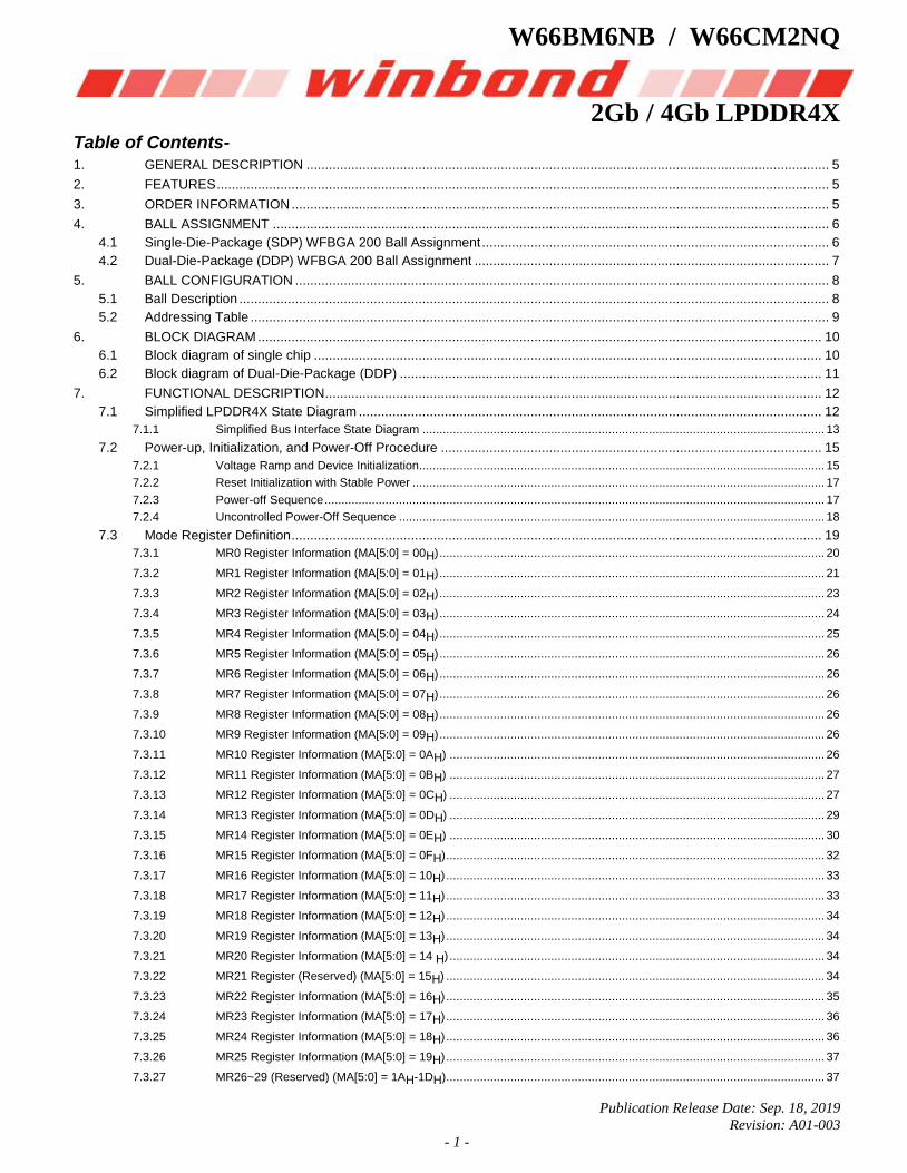
Table of Contents- 1. GENERAL DESCRIPTION ............................................................................................................................................ 5 2. FEATURES .................................................................................................................................................................... 5 3. ORDER INFORMATION ................................................................................................................................................ 5 4. BALL ASSIGNMENT ..................................................................................................................................................... 6
4.1 Single-Die-Package (SDP) WFBGA 200 Ball Assignment ............................................................................................. 6 4.2 Dual-Die-Package (DDP) WFBGA 200 Ball Assignment ............................................................................................... 7
5. BALL CONFIGURATION ............................................................................................................................................... 8 5.1 Ball Description .............................................................................................................................................................. 8 5.2 Addressing Table ........................................................................................................................................................... 9
6. BLOCK DIAGRAM ....................................................................................................................................................... 10 6.1 Block diagram of single chip ........................................................................................................................................ 10 6.2 Block diagram of Dual-Die-Package (DDP) ................................................................................................................. 11
7. FUNCTIONAL DESCRIPTION ..................................................................................................................................... 12 7.1 Simplified LPDDR4X State Diagram ............................................................................................................................ 12
7.1.1 Simplified Bus Interface State Diagram ....................................................................................................................... 13 7.2 Power-up, Initialization, and Power-Off Procedure ...................................................................................................... 15
7.2.1 Voltage Ramp and Device Initialization ........................................................................................................................ 15 7.2.2 Reset Initialization with Stable Power .......................................................................................................................... 17 7.2.3 Power-off Sequence .................................................................................................................................................... 17 7.2.4 Uncontrolled Power-Off Sequence .............................................................................................................................. 18
7.3 Mode Register Definition .............................................................................................................................................. 19 7.3.1 MR0 Register Information (MA[5:0] = 00H) .................................................................................................................. 20 7.3.2 MR1 Register Information (MA[5:0] = 01H) .................................................................................................................. 21 7.3.3 MR2 Register Information (MA[5:0] = 02H) .................................................................................................................. 23 7.3.4 MR3 Register Information (MA[5:0] = 03H) .................................................................................................................. 24 7.3.5 MR4 Register Information (MA[5:0] = 04H) .................................................................................................................. 25 7.3.6 MR5 Register Information (MA[5:0] = 05H) .................................................................................................................. 26 7.3.7 MR6 Register Information (MA[5:0] = 06H) .................................................................................................................. 26 7.3.8 MR7 Register Information (MA[5:0] = 07H) .................................................................................................................. 26 7.3.9 MR8 Register Information (MA[5:0] = 08H) .................................................................................................................. 26 7.3.10 MR9 Register Information (MA[5:0] = 09H) .................................................................................................................. 26 7.3.11 MR10 Register Information (MA[5:0] = 0AH) ............................................................................................................... 26 7.3.12 MR11 Register Information (MA[5:0] = 0BH) ............................................................................................................... 27 7.3.13 MR12 Register Information (MA[5:0] = 0CH) ............................................................................................................... 27 7.3.14 MR13 Register Information (MA[5:0] = 0DH) ............................................................................................................... 29 7.3.15 MR14 Register Information (MA[5:0] = 0EH) ............................................................................................................... 30 7.3.16 MR15 Register Information (MA[5:0] = 0FH) ................................................................................................................ 32 7.3.17 MR16 Register Information (MA[5:0] = 10H) ................................................................................................................ 33 7.3.18 MR17 Register Information (MA[5:0] = 11H) ................................................................................................................ 33 7.3.19 MR18 Register Information (MA[5:0] = 12H) ................................................................................................................ 34 7.3.20 MR19 Register Information (MA[5:0] = 13H) ................................................................................................................ 34 7.3.21 MR20 Register Information (MA[5:0] = 14 H) ............................................................................................................... 34 7.3.22 MR21 Register (Reserved) (MA[5:0] = 15H) ................................................................................................................ 34 7.3.23 MR22 Register Information (MA[5:0] = 16H) ................................................................................................................ 35 7.3.24 MR23 Register Information (MA[5:0] = 17H) ................................................................................................................ 36 7.3.25 MR24 Register Information (MA[5:0] = 18H) ................................................................................................................ 36 7.3.26 MR25 Register Information (MA[5:0] = 19H) ................................................................................................................ 37 7.3.27 MR26~29 (Reserved) (MA[5:0] = 1AH-1DH) ................................................................................................................ 37
W66BM6NB / W66CM2NQ
Publication Release Date: Sep. 18, 2019
Revision: A01-003
- 2 -
7.3.28 MR30 Register Information (MA[5:0] = 1EH) ............................................................................................................... 37 7.3.29 MR31 (Reserved) (MA[5:0] = 1FH) .............................................................................................................................. 37 7.3.30 MR32 Register Information (MA[5:0] = 20H) ................................................................................................................ 37 7.3.31 MR33~38 (Reserved) (MA[5:0] = 21H-26H) ................................................................................................................. 37 7.3.32 MR39 Register Information (MA[5:0] = 27H) ................................................................................................................ 38 7.3.33 MR40 Register Information (MA[5:0] = 28H) ................................................................................................................ 38
7.4 Command Definitions and Timing Diagrams ................................................................................................................ 39 7.4.1 Activate Command ...................................................................................................................................................... 39
7.4.1.1 8-Bank Device Operation .................................................................................................................................. 39 7.4.2 Core Timing ................................................................................................................................................................. 40 7.4.3 Read and Write Access Operations ............................................................................................................................. 41 7.4.4 Read Preamble and Postamble ................................................................................................................................... 41 7.4.5 Burst Read Operation .................................................................................................................................................. 42 7.4.6 Read Timing ................................................................................................................................................................ 46 7.4.7 tLZ(DQS), tLZ(DQ), tHZ(DQS), tHZ(DQ) Calculation ................................................................................................... 46
7.4.7.1 tLZ(DQS) and tHZ(DQS) Calculation for ATE (Automatic Test Equipment) ....................................................... 47 7.4.7.2 tLZ(DQ) and tHZ(DQ) Calculation for ATE (Automatic Test Equipment) ............................................................ 49 7.4.7.3 tRPRE Calculation for ATE (Automatic Test Equipment) ................................................................................... 51 7.4.7.4 tRPST Calculation for ATE (Automatic Test Equipment) ................................................................................... 52
7.4.8 tDQSCK Timing Table ................................................................................................................................................. 53 7.4.8.1 CK to DQS Rank to Rank variation ................................................................................................................... 53
7.4.9 Write Preamble and Postamble ................................................................................................................................... 54 7.4.10 Burst Write Operation .................................................................................................................................................. 55 7.4.11 Write Timing ................................................................................................................................................................ 58
7.4.11.1 tWPRE Calculation for ATE (Automatic Test Equipment) .................................................................................. 59 7.4.11.2 tWPST Calculation for ATE (Automatic Test Equipment) .................................................................................. 60
7.4.12 Read and Write Latencies ........................................................................................................................................... 61 7.4.13 Write and Masked Write operation DQS controls (WDQS Control) .............................................................................. 61
7.4.13.1 WDQS Control Mode 1 - Read Based Control ................................................................................................... 62 7.4.13.2 WDQS Control Mode 2 - WDQS_on/off ............................................................................................................ 62
7.4.14 Postamble and Preamble merging behavior ................................................................................................................ 67 7.4.14.1 Read to Read Operation ................................................................................................................................... 67 7.4.14.2 Write to Write Operation.................................................................................................................................... 80
7.4.15 Masked Write Operation .............................................................................................................................................. 90 7.4.15.1 Masked Write Timing constraints for BL16 ........................................................................................................ 92
7.4.16 LPDDR4X Data Mask (DM) and Data Bus Inversion (DBIdc) Function ........................................................................ 94 7.4.17 Precharge Operation ................................................................................................................................................... 97
7.4.17.1 Burst Read Operation Followed by a Precharge ............................................................................................... 98 7.4.17.2 Burst Write Operation Followed by a Precharge ................................................................................................ 99 7.4.17.3 Auto-Precharge Operation ................................................................................................................................ 99 7.4.17.4 Burst Read with Auto-Precharge ..................................................................................................................... 100 7.4.17.5 Burst Write with Auto-Precharge ..................................................................................................................... 101
7.4.18 Auto-Precharge Operation ......................................................................................................................................... 102 7.4.18.1 Delay time from Write to Read with Auto-Precharge ....................................................................................... 103
7.4.19 Refresh command ..................................................................................................................................................... 107 7.4.19.1 Burst Read operation followed by Per Bank Refresh ....................................................................................... 113
7.4.20 Refresh Requirement ................................................................................................................................................ 114 7.4.21 Self Refresh Operation .............................................................................................................................................. 115
7.4.21.1 Self Refresh Entry and Exit ............................................................................................................................. 115 7.4.21.2 Power Down Entry and Exit during Self Refresh ............................................................................................. 116 7.4.21.3 Command input Timing after Power Down Exit ............................................................................................... 117 7.4.21.4 AC Timing Table ............................................................................................................................................. 118
7.4.22 MRR, MRW, MPC Command during tXSR, tRFC ...................................................................................................... 119 7.4.23 MODE REGISTER READ (MRR) .............................................................................................................................. 120
7.4.23.1 MRR after Read and Write command ............................................................................................................. 122 7.4.23.2 MRR after Power-Down Exit ........................................................................................................................... 124
W66BM6NB / W66CM2NQ
Publication Release Date: Sep. 18, 2019
Revision: A01-003
- 3 -
7.4.24 Mode Register Write (MRW) Operation ..................................................................................................................... 125 7.4.24.1 Mode Register Write ....................................................................................................................................... 125
7.4.25 VREF Current Generator (VRCG) ............................................................................................................................. 127 7.4.26 CA VREF Training ..................................................................................................................................................... 128 7.4.27 DQ VREF Training .................................................................................................................................................... 133 7.4.28 Command Bus Training ............................................................................................................................................. 138
7.4.28.1 Training Sequence for single-rank systems ..................................................................................................... 139 7.4.28.2 Training Sequence for multi-rank systems ...................................................................................................... 139 7.4.28.3 Relation between CA input pin DQ output pin ................................................................................................. 140 7.4.28.4 Timing Diagram .............................................................................................................................................. 140 7.4.28.5 Command Bus Training AC Timing Table ....................................................................................................... 145
7.4.29 Frequency Set Point .................................................................................................................................................. 146 7.4.29.1 Frequency set point update Timing ................................................................................................................. 147
7.4.30 Mode Register Write-WR Leveling Mode ................................................................................................................... 151 7.4.30.1 Write Leveling Procedure ................................................................................................................................ 151 7.4.30.2 Input Clock Frequency Stop and Change ........................................................................................................ 153 7.4.30.3 Write Leveling Setup and Hold Time ............................................................................................................... 154
7.4.31 RD DQ Calibration ..................................................................................................................................................... 155 7.4.31.1 RD DQ Calibration Training Procedure ........................................................................................................... 155 7.4.31.2 DQ Read Training Example ............................................................................................................................ 158 7.4.31.3 MPC of Read DQ Calibration after Power-Down Exit ...................................................................................... 159
7.4.32 DQS-DQ Training ...................................................................................................................................................... 160 7.4.32.1 FIFO Pointer Reset and Synchronism ............................................................................................................. 161
7.4.33 DQS Interval Oscillator .............................................................................................................................................. 166 7.4.33.1 Interval Oscillator matching error .................................................................................................................... 168 7.4.33.2 DQS Interval Oscillator Readout Timing .......................................................................................................... 169
7.4.34 READ Preamble Training .......................................................................................................................................... 171 7.4.35 Multi-Purpose Command (MPC) ................................................................................................................................ 172 7.4.36 Thermal Offset .......................................................................................................................................................... 176 7.4.37 Temperature Sensor.................................................................................................................................................. 176 7.4.38 ZQ Calibration ........................................................................................................................................................... 178
7.4.38.1 ZQCal Reset ................................................................................................................................................... 178 7.4.38.2 ZQ External Resistor, Tolerance, and Capacitive Loading .............................................................................. 179
7.4.39 Pull Up/Pull Down Driver Characteristics and Calibration........................................................................................... 179 7.4.40 On Die Termination for Command/Address Bus ........................................................................................................ 180
7.4.40.1 ODT Mode Register and ODT State Table ...................................................................................................... 180 7.4.40.2 ODT Mode Register and ODT Characteristics................................................................................................. 181 7.4.40.3 ODT for Command/Address update time ........................................................................................................ 183
7.4.41 On-Die Termination ................................................................................................................................................... 184 7.4.41.1 ODT Mode Register ........................................................................................................................................ 184 7.4.41.2 Asynchronous ODT......................................................................................................................................... 184 7.4.41.3 ODT during Write Leveling .............................................................................................................................. 186
7.4.42 On Die Termination for DQ, DQS and DMI ................................................................................................................ 187 7.4.43 Output Driver and Termination Register Temperature and Voltage Sensitivity ........................................................... 189 7.4.44 Power-Down Mode .................................................................................................................................................... 190
7.4.44.1 Power-Down Entry and Exit ............................................................................................................................ 190 7.4.45 Input Clock Stop and Frequency Change .................................................................................................................. 197 7.4.46 Truth Tables .............................................................................................................................................................. 199 7.4.47 TRR Mode - Target Row Refresh .............................................................................................................................. 201
7.4.47.1 TRR Mode Operation ...................................................................................................................................... 201 7.4.48 Post Package Repair (PPR) ...................................................................................................................................... 203
7.4.48.1 Fail Row Address Repair ................................................................................................................................ 203 8. ELECTRICAL CHARACTERISTIC ............................................................................................................................ 205
8.1 Absolute Maximum DC Ratings ................................................................................................................................. 205 8.2 AC & DC Operating Conditions .................................................................................................................................. 205
8.2.1 Recommended DC Operating Conditions .................................................................................................................. 205 8.2.2 Input Leakage Current ............................................................................................................................................... 205
W66BM6NB / W66CM2NQ
Publication Release Date: Sep. 18, 2019
Revision: A01-003
- 4 -
8.2.3 Input/Output Leakage Current ................................................................................................................................... 205 8.2.4 Operating Temperature Range .................................................................................................................................. 206
8.3 AC and DC Input/Output Measurement levels ........................................................................................................... 206 8.3.1 1.1 V High speed LVCMOS (HS_LLVCMOS) ............................................................................................................ 206
8.3.1.1 Standard specifications ................................................................................................................................... 206 8.3.1.2 DC electrical characteristics ............................................................................................................................ 206 8.3.1.2.1 LPDDR4X Input Level for CKE ........................................................................................................................ 206 8.3.1.2.2 LPDDR4X Input Level for Reset_n and ODT_CA ............................................................................................ 207 8.3.1.3 AC Over/Undershoot ....................................................................................................................................... 207 8.3.1.3.1 LPDDR4X AC Over/Undershoot ..................................................................................................................... 207
8.3.2 Differential Input Voltage ........................................................................................................................................... 208 8.3.2.1 Differential Input Voltage for CK ...................................................................................................................... 208 8.3.2.2 Peak voltage calculation method ..................................................................................................................... 209 8.3.2.3 Single-Ended Input Voltage for Clock .............................................................................................................. 210 8.3.2.4 Differential Input Slew Rate Definition for Clock .............................................................................................. 211 8.3.2.5 Differential Input Cross Point Voltage .............................................................................................................. 212 8.3.2.6 Differential Input Voltage for DQS ................................................................................................................... 213 8.3.2.7 Peak voltage calculation method ..................................................................................................................... 214 8.3.2.8 Single-Ended Input Voltage for DQS ............................................................................................................... 215 8.3.2.9 Differential Input Slew Rate Definition for DQS ............................................................................................... 216 8.3.2.10 Differential Input Cross Point Voltage .............................................................................................................. 217
8.3.3 Input level for ODT_CA input ..................................................................................................................................... 218 8.3.4 Single Ended Output Slew Rate ................................................................................................................................ 218 8.3.5 Differential Output Slew Rate .................................................................................................................................... 219 8.3.6 Overshoot and Undershoot for LVSTL ....................................................................................................................... 220 8.3.7 LPDDR4X Driver Output Timing Reference load ....................................................................................................... 221 8.3.8 LVSTL (Low Voltage Swing Terminated Logic) IO System ........................................................................................ 221
8.4 Input/Output Capacitance .......................................................................................................................................... 223 8.5 IDD Specification Parameters and Test Conditions ................................................................................................... 224
8.5.1 IDD Measurement Conditions .................................................................................................................................... 224 8.5.2 IDD Specifications ..................................................................................................................................................... 230
8.6 Electrical Characteristics and AC Timing ................................................................................................................... 236 8.6.1 Clock Specification .................................................................................................................................................... 236
8.6.1.1 Definition for tCK(avg) and nCK ...................................................................................................................... 236 8.6.1.2 Definition for tCK(abs) ..................................................................................................................................... 236 8.6.1.3 Definition for tCH(avg) and tCL(avg) ............................................................................................................... 237 8.6.1.4 Definition for tCH(abs) and tCL(abs) ............................................................................................................... 237 8.6.1.5 Definition for tJIT(per) ..................................................................................................................................... 237 8.6.1.6 Definition for tJIT(cc) ....................................................................................................................................... 237
8.6.2 Clock AC Timing ........................................................................................................................................................ 238 8.6.3 Temperature Derating for AC timing .......................................................................................................................... 238 8.6.4 CA Rx voltage and timing .......................................................................................................................................... 239 8.6.5 DRAM Data Timing ................................................................................................................................................... 242 8.6.6 DQ Rx voltage and timing .......................................................................................................................................... 244
9. PACKAGE DIMENSIONS .......................................................................................................................................... 248 10. REVISION HISTORY ................................................................................................................................................. 249
W66BM6NB / W66CM2NQ
Publication Release Date: Sep. 18, 2019
Revision: A01-003
- 5 -
1. GENERAL DESCRIPTION
This datasheet is covering LPDDR4X device with either one of following configurations.
Single-Die-Package (SDP) 16Mb x 16DQ x 8-banks x 1 channel with 2 Gb (2,147,483,648 bits) density.
Dual-Die-Package (DDP) 16Mb x 16DQ x 8-banks x 2 channels with 4 Gb (4,294,967,296 bits) density.
This LPDDR4X device uses a 2 or 4 clocks architecture on the Command/Address (CA) bus to reduce the number of input pins in the system. The 6-bit CA bus contains command, address, and bank information. Each command uses 1, 2 or 4 clock cycle, during which command information is transferred on the positive edge of the clock. See command truth table for details. See command truth table for details.
2. FEATURES
VDD1 = 1.7~1.95V
VDD2 = 1.06V~1.17V
VDDQ = 0.57V~0.65V
Data width: x16/x32
Clock rate: up to 2133 MHz
Data rate: up to 4267 Mbps
8 internal banks for concurrent operation
16n pre-fetch operation
Interface: LVSTL_11
Burst length: 16, 32, on-the-fly 16 or 32
Burst type: Sequential
Programmable Driver strength
Coded command input in double clock edges
Single data rate architecture on the CA bus
Double data rate architecture on the DQ pins
Differential clock input
Bidirectional differential data strobe
Input clock stop and frequency change
On-die termination (ODT)
Write leveling support
Programmable Read and Write Latencies (RL/WL)
CA training support
DQ-DQS training
Refresh feature:
- Auto Refresh (per bank / all bank)
- Partial array self-refresh
- Auto temperature compensated self-refresh
Post Package Repair
Target Row Refresh Mode
Frequency-Set-Points for fast frequency switch
Support write mask and data bus inversion(DBI)
Support Boundary Scan for connectivity test*
Support package:
WFBGA 200 Ball (10x14.5mm2)
Operating Temperature Range:
-40°C ≤ TCASE ≤ 95°C
-40°C ≤ TCASE ≤ 105°C
0°C ≤ TCASE ≤ 70°C
* For further information about Boundary Scan for connectivity test, please contact sales representative.
3. ORDER INFORMATION
Part Number VDD1/VDD2/VDDQ I/O Width Type Others
W66BM6NBUAFI 1.8V/1.1V/0.6V 16 WFBGA 200 ball (SDP) LPDDR4X-3200, -40°C~95°C
W66BM6NBUAGI 1.8V/1.1V/0.6V 16 WFBGA 200 ball (SDP) LPDDR4X-3733, -40°C~95°C
W66BM6NBUAHI 1.8V/1.1V/0.6V 16 WFBGA 200 ball (SDP) LPDDR4X-4267, -40°C~95°C
W66CM2NQUAFI 1.8V/1.1V/0.6V 32 WFBGA 200 ball (DDP) LPDDR4X-3200, -40°C~95°C
W66CM2NQUAGI 1.8V/1.1V/0.6V 32 WFBGA 200 ball (DDP) LPDDR4X-3733, -40°C~95°C
W66CM2NQUAHI 1.8V/1.1V/0.6V 32 WFBGA 200 ball (DDP) LPDDR4X-4267, -40°C~95°C
W66BM6NBUAFJ 1.8V/1.1V/0.6V 16 WFBGA 200 ball (SDP) LPDDR4X-3200, -40°C~105°C
W66BM6NBUAGJ 1.8V/1.1V/0.6V 16 WFBGA 200 ball (SDP) LPDDR4X-3733, -40°C~105°C
W66BM6NBUAHJ 1.8V/1.1V/0.6V 16 WFBGA 200 ball (SDP) LPDDR4X-4267, -40°C~105°C
W66CM2NQUAFJ 1.8V/1.1V/0.6V 32 WFBGA 200 ball (DDP) LPDDR4X-3200, -40°C~105°C
W66CM2NQUAGJ 1.8V/1.1V/0.6V 32 WFBGA 200 ball (DDP) LPDDR4X-3733, -40°C~105°C
W66CM2NQUAHJ 1.8V/1.1V/0.6V 32 WFBGA 200 ball (DDP) LPDDR4X-4267, -40°C~105°C
W66CM2NQUAHC 1.8V/1.1V/0.6V 32 WFBGA 200 ball (DDP) LPDDR4X-4267, 0°C~70°C
W66BM6NB / W66CM2NQ
Publication Release Date: Sep. 18, 2019
Revision: A01-003
- 6 -
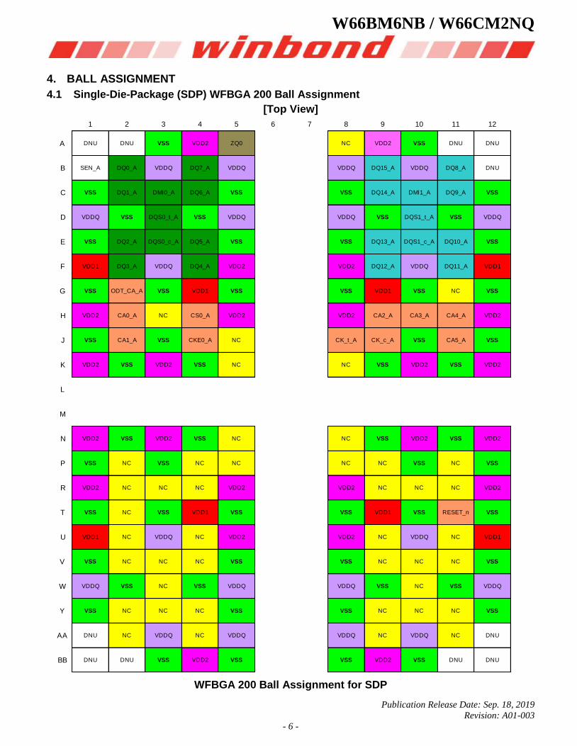
4. BALL ASSIGNMENT
4.1 Single-Die-Package (SDP) WFBGA 200 Ball Assignment
[Top View]
1 2 3 4 5 6 7 8 9 10 11 12
A DNU DNU VSS VDD2 ZQ0 NC VDD2 VSS DNU DNU
B SEN_A DQ0_A VDDQ DQ7_A VDDQ VDDQ DQ15_A VDDQ DQ8_A DNU
C VSS DQ1_A DMI0_A DQ6_A VSS VSS DQ14_A DMI1_A DQ9_A VSS
D VDDQ VSS DQS0_t_A VSS VDDQ VDDQ VSS DQS1_t_A VSS VDDQ
E VSS DQ2_A DQS0_c_A DQ5_A VSS VSS DQ13_A DQS1_c_A DQ10_A VSS
F VDD1 DQ3_A VDDQ DQ4_A VDD2 VDD2 DQ12_A VDDQ DQ11_A VDD1
G VSS ODT_CA_A VSS VDD1 VSS VSS VDD1 VSS NC VSS
H VDD2 CA0_A NC CS0_A VDD2 VDD2 CA2_A CA3_A CA4_A VDD2
J VSS CA1_A VSS CKE0_A NC CK_t_A CK_c_A VSS CA5_A VSS
K VDD2 VSS VDD2 VSS NC NC VSS VDD2 VSS VDD2
L
M
N VDD2 VSS VDD2 VSS NC NC VSS VDD2 VSS VDD2
P VSS NC VSS NC NC NC NC VSS NC VSS
R VDD2 NC NC NC VDD2 VDD2 NC NC NC VDD2
T VSS NC VSS VDD1 VSS VSS VDD1 VSS RESET_n VSS
U VDD1 NC VDDQ NC VDD2 VDD2 NC VDDQ NC VDD1
V VSS NC NC NC VSS VSS NC NC NC VSS
W VDDQ VSS NC VSS VDDQ VDDQ VSS NC VSS VDDQ
Y VSS NC NC NC VSS VSS NC NC NC VSS
AA DNU NC VDDQ NC VDDQ VDDQ NC VDDQ NC DNU
BB DNU DNU VSS VDD2 VSS VSS VDD2 VSS DNU DNU
WFBGA 200 Ball Assignment for SDP
W66BM6NB / W66CM2NQ
Publication Release Date: Sep. 18, 2019
Revision: A01-003
- 7 -
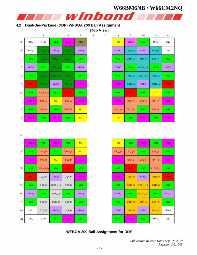
4.2 Dual-Die-Package (DDP) WFBGA 200 Ball Assignment
[Top View]
1 2 3 4 5 6 7 8 9 10 11 12
A DNU DNU VSS VDD2 ZQ0 NC VDD2 VSS DNU DNU
B SEN_A DQ0_A VDDQ DQ7_A VDDQ VDDQ DQ15_A VDDQ DQ8_A DNU
C VSS DQ1_A DMI0_A DQ6_A VSS VSS DQ14_A DMI1_A DQ9_A VSS
D VDDQ VSS DQS0_t_A VSS VDDQ VDDQ VSS DQS1_t_A VSS VDDQ
E VSS DQ2_A DQS0_c_A DQ5_A VSS VSS DQ13_A DQS1_c_A DQ10_A VSS
F VDD1 DQ3_A VDDQ DQ4_A VDD2 VDD2 DQ12_A VDDQ DQ11_A VDD1
G VSS ODT_CA_A VSS VDD1 VSS VSS VDD1 VSS NC VSS
H VDD2 CA0_A NC CS0_A VDD2 VDD2 CA2_A CA3_A CA4_A VDD2
J VSS CA1_A VSS CKE0_A NC CK_t_A CK_c_A VSS CA5_A VSS
K VDD2 VSS VDD2 VSS NC NC VSS VDD2 VSS VDD2
L
M
N VDD2 VSS VDD2 VSS NC NC VSS VDD2 VSS VDD2
P VSS CA1_B VSS CKE0_B NC CK_t_B CK_c_B VSS CA5_B VSS
R VDD2 CA0_B NC CS0_B VDD2 VDD2 CA2_B CA3_B CA4_B VDD2
T VSS ODT_CA_B VSS VDD1 VSS VSS VDD1 VSS RESET_n VSS
U VDD1 DQ3_B VDDQ DQ4_B VDD2 VDD2 DQ12_B VDDQ DQ11_B VDD1
V VSS DQ2_B DQS0_c_B DQ5_B VSS VSS DQ13_B DQS1_c_B DQ10_B VSS
W VDDQ VSS DQS0_t_B VSS VDDQ VDDQ VSS DQS1_t_B VSS VDDQ
Y VSS DQ1_B DMI0_B DQ6_B VSS VSS DQ14_B DMI1_B DQ9_B VSS
AA DNU DQ0_B VDDQ DQ7_B VDDQ VDDQ DQ15_B VDDQ DQ8_B SEN_B
BB DNU DNU VSS VDD2 VSS VSS VDD2 VSS DNU DNU
WFBGA 200 Ball Assignment for DDP
W66BM6NB / W66CM2NQ
Publication Release Date: Sep. 18, 2019
Revision: A01-003
- 8 -
5. BALL CONFIGURATION
5.1 Ball Description
Name Type Description
CK_t_A, CK_c_A,
CK_t_B, CK_c_B Input
Clock: CK_t and CK_c are differential clock inputs. All address, command, and control input signals are sampled on the crossing of the positive edge of CK_t and the negative edge of CK_c. AC timings for CA parameters are referenced to CK. Each channel (A & B) has its own clock pair.
CKE_A, CKE_B Input Clock Enable: CKE HIGH activates and CKE LOW deactivates the internal clock circuits, input buffers, and output drivers. Power-saving modes are entered and exited via CKE transitions. Each channel (A & B) has its own CKE signal.
CS_A, CS_B Input Chip Select: CS is part of the command code. Each channel (A & B) has its own CS signal.
CA[5:0]_A, CA[5:0]_B
Input Command/Address Inputs: CA signals provide the Command and Address inputs according to the Command Truth Table. Each channel (A & B) has its own CA signals.
ODT_CA_A, ODT_CA_B
Input CA ODT Control: The ODT_CA pin is ignored by LPDDR4X devices. ODT-CS/CA/CK function is fully controlled through MR11 and MR22. The ODT_CA pin shall be connected to either VDD2 or VSS.
DQ[15:0]_A, DQ[15:0]_B
I/O Data Inputs/Output: Bi-directional data bus.
DQS[1:0]_t_A, DQS[1:0]_c_A,
DQS[1:0]_t_B, DQS[1:0]_c_B
I/O
Data Strobe: DQS_t and DQS_c are bi-directional differential output clock signals used to strobe data during a READ or WRITE. The Data Strobe is generated by the DRAM for a READ and is edge-aligned with Data. The Data Strobe is generated by the Memory Controller for a WRITE and must arrive prior to Data. Each byte of data has a Data Strobe signal pair. Each channel (A & B) has its own DQS strobes.
DMI[1:0]_A, DMI[1:0]_B
I/O
Data Mask Inversion: DMI is a bi-directional signal which is driven HIGH when the data on the data bus is inverted, or driven LOW when the data is in its normal state. Data Inversion can be disabled via a mode register setting. Each byte of data has a DMI signal. Each channel (A & B) has its own DMI signals. This signal is also used along with the DQ signals to provide write data masking information to the DRAM. The DMI pin function - Data Inversion or Data mask - depends on Mode Register setting.
RESET_n Input RESET: When asserted LOW, the RESET_n signal resets all channels of the die. There is one RESET_n pad per die.
VDDQ, VDD1, VDD2
Supply Power Supplies: Isolated on the die for improved noise immunity.
VSS, VSSQ Supply Ground Reference: Power supply ground reference.
ZQ0 Reference Calibration Reference: Used to calibrate the output drive strength and the termination resistance. The ZQ0 pin shall be connected to VDDQ through a 240Ω ± 1% resistor.
SEN Input Scan Enable: SEN must be asserted HIGH for enabling boundary scan function. Must be tied to Ground or NC (No Connection) when not in use.
DNU -- Do Not Use
NC -- No connect: Not internally connected.
Note:
1. "_A" and "_B" indicate DRAM channel. "_A" pads are present in all devices. "_B" pads are present in dual channel DRAM devices only.
W66BM6NB / W66CM2NQ
Publication Release Date: Sep. 18, 2019
Revision: A01-003
- 9 -
5.2 Addressing Table
128M x 16 128M x 32
Die per package 1 2
Memory Density (per package) 2 Gb 4 Gb
Memory Density (per die) 2 Gb 2 Gb
Memory Density (per channel) 2 Gb 2 Gb
Configuration 16Mb x 16DQ x 8 banks
x 1 channel 16Mb x 16DQ x 8 banks
x 2 channels
Number of Channels (per die) 1 1
Number of Banks (per channel) 8 8
Array Pre-Fetch (bits, per channel) 256 256
Number of Rows (per channel) 16384 16384
Number of Columns (fetch boundaries) 64 64
Page Size (Bytes) 2048 2048
Bank Address BA0 – BA2 BA0 – BA2
x16
Row Addresses R0 – R13 R0 – R13
Column Addresses C0 – C9 C0 – C9
Burst Starting Address Boundary 64 bit 64 bit
Note:
1. The lower two column addresses (C0 - C1) are assumed to be “zero” and are not transmitted on the CA bus.
W66BM6NB / W66CM2NQ
Publication Release Date: Sep. 18, 2019
Revision: A01-003
- 10 -
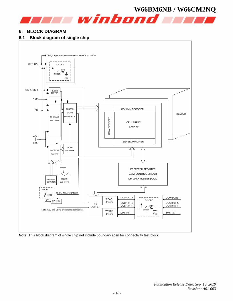
6. BLOCK DIAGRAM
6.1 Block diagram of single chip
CKE
CLOCK
BUFFER
COMMAND
DECODER
BUFFER
REFRESH
COUNTER
COLUMN
COUNTER
SIGNAL
GENERATOR
MODE
REGISTER
DQ
BUFFER
CS
WRITE
drivers
READ
drivers
COLUMN DECODER
SENSE AMPLIFIER
CELL ARRAY
BANK #0
BANK #7
VSS
Swtich
CA ODT
RTT
DATA CONTROL CIRCUIT
DM MASK Inversion LOGIC
PREFETCH REGISTER
CK_c, CK_t
DQ0−DQ15
CONTROL
ZQCAL, ZQLAT, ZQRESET
ZQ CAL
RZQ
ZQ
VDDQ
CA0
CA5
ADDRESS
RO
W D
EC
OD
ER
Note: RZQ and VDDQ are external component
DMI[1:0]
DQS[1:0]_c,
DQS[1:0]_t
ODT_CA
ODT_CA pin shall be connected to either VDD2 or VSS
VSS
Swtich
DQ ODT
RTT
DQ0−DQ15
DQS[1:0]_c,
DQS[1:0]_t
DMI[1:0]
Note: This block diagram of single chip not include boundary scan for connectivity test block.
W66BM6NB / W66CM2NQ
Publication Release Date: Sep. 18, 2019
Revision: A01-003
- 11 -
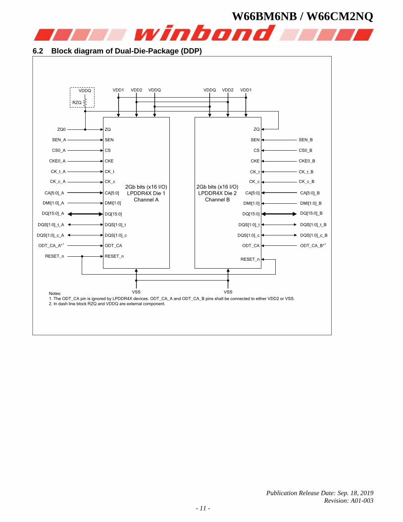
6.2 Block diagram of Dual-Die-Package (DDP)
VDD1 VDD2 VDDQ
VSS
CS0_A
CKE0_A
CK_t_A
CK_c_A
CA[5:0]_A
DMI[1:0]_A
DQ[15:0]_A
DQS[1:0]_t_A
DQS[1:0]_c_A
ODT_CA_A*1
ZQ0
RESET_n
CS
CKE
CK_t
CK_c
CA[5:0]
DMI[1:0]
DQ[15:0]
DQS[1:0]_t
DQS[1:0]_c
ODT_CA
ZQ
RESET_n
2Gb bits (x16 I/O)
LPDDR4X Die 1
Channel A
VDD1VDD2VDDQ
VSS
CS0_B
CKE0_B
CK_t_B
CK_c_B
CA[5:0]_B
DMI[1:0]_B
DQ[15:0]_B
DQS[1:0]_t_B
DQS[1:0]_c_B
ODT_CA_B*1
CS
CKE
CK_t
CK_c
CA[5:0]
DMI[1:0]
DQ[15:0]
DQS[1:0]_t
DQS[1:0]_c
ODT_CA
ZQ
RESET_n
RZQ
VDDQ
Notes:
1. The ODT_CA pin is ignored by LPDDR4X devices. ODT_CA_A and ODT_CA_B pins shall be connected to either VDD2 or VSS.
2. In dash line block RZQ and VDDQ are external component.
SEN_A SEN SEN_BSEN
2Gb bits (x16 I/O)
LPDDR4X Die 2
Channel B
W66BM6NB / W66CM2NQ
Publication Release Date: Sep. 18, 2019
Revision: A01-003
- 12 -
7. FUNCTIONAL DESCRIPTION
For this LPDDR4X device, accesses begin with the registration of an Activate command, which is then followed by a Read or Write command. The address and BA bits registered coincident with the Activate command are used to select the row and the Bank to be accessed. The address bits registered coincident with the Read or Write command are used to select the Bank and the starting column location for the burst access.
This device also uses double data rate architecture on the DQ pins to achieve high speed operation. The double data rate architecture is essentially a 16n prefetch architecture with an interface designed to transfer two data bits per DQ every clock cycle at the I/O pins. A single read or write access for the LPDDR4X SDRAM effectively consists of a single 16n-bit wide, one clock cycle data transfer at the internal DRAM core and eight corresponding n-bit wide, one-half-clock-cycle data transfers at the I/O pins.
Read and write accesses to this LPDDR4X SDRAMs are burst oriented; accesses start at a selected location and continue for a programmed number of locations in a programmed sequence. Prior to normal operation, this LPDDR4X SDRAM must be initialized. The following section provides detailed information covering device initialization, register definition, command description and device operation.
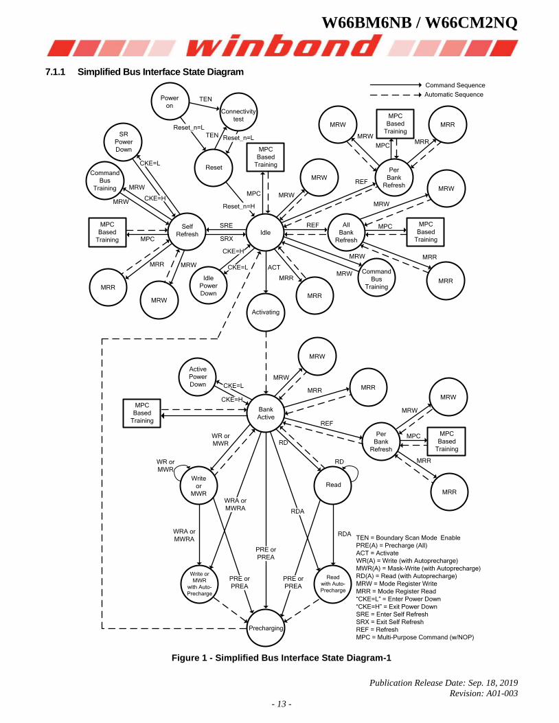
7.1 Simplified LPDDR4X State Diagram
LPDDR4X-SDRAM state diagram provides a simplified illustration of allowed state transitions and the related commands to control them. For a complete definition of the device behavior, the information provided by the state diagram should be integrated with the truth tables and timing specification.
The truth tables provide complementary information to the state diagram; they clarify the device behavior and the applied restrictions when considering the actual state of all the banks.
For the command definition, see chapter 7.4 “Command Definitions and Timing Diagrams”.
W66BM6NB / W66CM2NQ
Publication Release Date: Sep. 18, 2019
Revision: A01-003
- 13 -
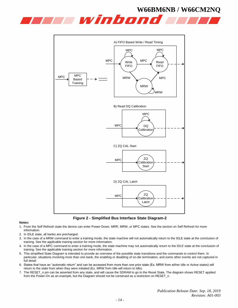
7.1.1 Simplified Bus Interface State Diagram
SR
Power
Down
Command
Bus
Training
Power
on
Self
Refresh
MPC
Based
Training
MPC
Based
Training
MPC
Based
Training
MPC
Based
Training
Reset
Idle
MRW
MRW
MRW
MRR
MRR
MRWMRR
MRR
MRR
MRR
MRW
MRW
Idle
Power
Down
Active
Power
Down
Activating
All
Bank
Refresh
Per
Bank
Refresh
Command
Bus
Training
Per
Bank
Refresh
MPC
Based
Training
Bank
Active
MPC
Based
Training
Write
or
MWR
Write or
MWR
with Auto-
Precharge
Read
with Auto-
Precharge
Precharging
Read
Command Sequence
Automatic Sequence
MRRMRW
MRW
REF
MRW
MRRMRW
MRWMRR
ACTMRWMRR
MRW
MPC
SRE
SRX
MPC
MPCREF
MRW
MRW
MRR
REF
Reset_n=L
Reset_n=H
CKE=L
CKE=H
MPC
MRW
MPC
MRR
RDA
RDA
WRA or
MWRA
PRE or
PREA
PRE or
PREA
PRE or
PREA
WRA or
MWRA
WR or
MWR
WR or
MWR
RD
RD
TEN = Boundary Scan Mode Enable
PRE(A) = Precharge (All)
ACT = Activate
WR(A) = Write (with Autoprecharge)
MWR(A) = Mask-Write (with Autoprecharge)
RD(A) = Read (with Autoprecharge)
MRW = Mode Register Write
MRR = Mode Register Read
“CKE=L” = Enter Power Down
“CKE=H” = Exit Power Down
SRE = Enter Self Refresh
SRX = Exit Self Refresh
REF = Refresh
MPC = Multi-Purpose Command (w/NOP)
CKE=H
CKE=L
CKE=H
CKE=L
Connectivity
test
TEN
TEN
Reset_n=L
Figure 1 - Simplified Bus Interface State Diagram-1
W66BM6NB / W66CM2NQ
Publication Release Date: Sep. 18, 2019
Revision: A01-003
- 14 -
Write
FIFO
Read
FIFO
MRW
DQ
Calibration
ZQ
Calibration
Start
ZQ
Calibration
Latch
MPC
MPC
MPC
MRW
MPC MPC
MPC
MPC
MRW
D) ZQ CAL Latch
C) ZQ CAL Start
B) Read DQ Calibration
MPC
A) FIFO Based Write / Read Timing
MPC
MPC
Based
Training
MPC
Figure 2 - Simplified Bus Interface State Diagram-2
Notes:
1. From the Self Refresh state the device can enter Power-Down, MRR, MRW, or MPC states. See the section on Self Refresh for more information.
2. In IDLE state, all banks are precharged.
3. In the case of a MRW command to enter a training mode, the state machine will not automatically return to the IDLE state at the conclusion of training. See the applicable training section for more information.
4. In the case of a MPC command to enter a training mode, the state machine may not automatically return to the IDLE state at the conclusion of training. See the applicable training section for more information.
5. This simplified State Diagram is intended to provide an overview of the possible state transitions and the commands to control them. In particular, situations involving more than one bank, the enabling or disabling of on-die termination, and some other events are not captured in full detail.
6. States that have an “automatic return” and can be accessed from more than one prior state (Ex. MRW from either Idle or Active states) will return to the state from when they were initiated (Ex. MRW from Idle will return to Idle).
7. The RESET_n pin can be asserted from any state, and will cause the SDRAM to go to the Reset State. The diagram shows RESET applied from the Power-On as an example, but the Diagram should not be construed as a restriction on RESET_n.
W66BM6NB / W66CM2NQ
Publication Release Date: Sep. 18, 2019
Revision: A01-003
- 15 -
7.2 Power-up, Initialization, and Power-Off Procedure
For power-up and reset initialization, in order to prevent DRAM from functioning improperly, default values of the following MR settings are defined as the table below.
Table 1 - MRS defaults settings
Item MRS Default Setting Description
FSP-OP/WR MR13 OP[7:6] 00b FSP-OP/WR[0] are enabled
WLS MR2 OP[6] 0b Write Latency Set A is selected
WL MR2 OP[5:3] 000b WL = 4
RL MR2 OP[2:0] 000b RL = 6, nRTP=8
nWR MR1 OP[6:4] 000b nWR = 6
DBI-WR/RD MR3 OP[7:6] 00b Write & Read DBI are disabled
CA ODT MR11 OP[6:4] 000b CA ODT is disabled
DQ ODT MR11 OP[2:0] 000b DQ ODT is disabled
VREF(CA) Setting MR12 OP[6] 1b VREF(CA) Range[1] enabled
VREF(CA) Value MR12 OP[5:0] 011101b Range1 : 50.3% of VDDQ
VREF(DQ) Setting MR14 OP[6] 1b VREF(DQ) Range[1] enabled
VREF(DQ) Value MR14 OP[5:0] 011101b Range1 : 50.3% of VDDQ
7.2.1 Voltage Ramp and Device Initialization
The following sequence shall be used to power up the LPDDR4X device. Unless specified otherwise, these steps are mandatory. Note that the power-up sequence of all channels must proceed simultaneously.
1. While applying power (after Ta), RESET_n is recommended to be LOW (≤ 0.2 x VDD2) and all other inputs must be between VILmin and VIHmax. The device outputs remain at High-Z while RESET_n is held LOW. Power supply voltage ramp requirements are provided in Table 2. VDD1 must ramp at the same time or earlier than VDD2. VDD2 must ramp at the same time or earlier than VDDQ.
Table 2 - Voltage Ramp Conditions
After Applicable Conditions
Ta is reached VDD1 must be greater than VDD2
VDD2 must be greater than VDDQ—200mV
Notes:
1. Ta is the point when any power supply first reaches 300 mV.
2. Noted voltage ramp conditions apply between Ta and power-off (controlled or uncontrolled).
3. Tb is the point at which all supply and reference voltages are within their defined ranges.
4. Power ramp duration tINIT0 (Tb - Ta) must not exceed 20 mS.
5. The voltage difference between of VSS and VSSQ pin must not exceed 100 mV.
2. Following the completion of the voltage ramp (Tb), RESET_n must be maintained LOW. DQ, DMI, DQS_t and DQS_c voltage levels must be between VSSQ and VDDQ during voltage ramp to avoid latch-up. CKE, CK_t, CK_c, CS_n and CA input levels must be between VSS and VDD2 during voltage ramp to avoid latch-up.
3. Beginning at Tb, RESET_n must remain LOW for at least tINIT1 (Tc), after which RESET_n can be deasserted to HIGH (Tc). At least 10ns before RESET_n de-assertion, CKE is required to be set LOW. All other input signals are "Don't Care".
4. After RESET_n is de-asserted (Tc), wait at least tINIT3 before activating CKE. Clock (CK_t, CK_c) is required to be started and stabilized for tINIT4 before CKE goes active (Td). CS is required to be maintained LOW when controller activates CKE.
5. After setting CKE high, wait minimum of tINIT5 to issue any MRR or MRW commands (Te). For both MRR and MRW commands, the clock frequency must be within the range defined for tCKb. Some AC parameters (for example, tDQSCK) could have relaxed timings (such as tDQSCKb) before the system is appropriately configured.
W66BM6NB / W66CM2NQ
Publication Release Date: Sep. 18, 2019
Revision: A01-003
- 16 -
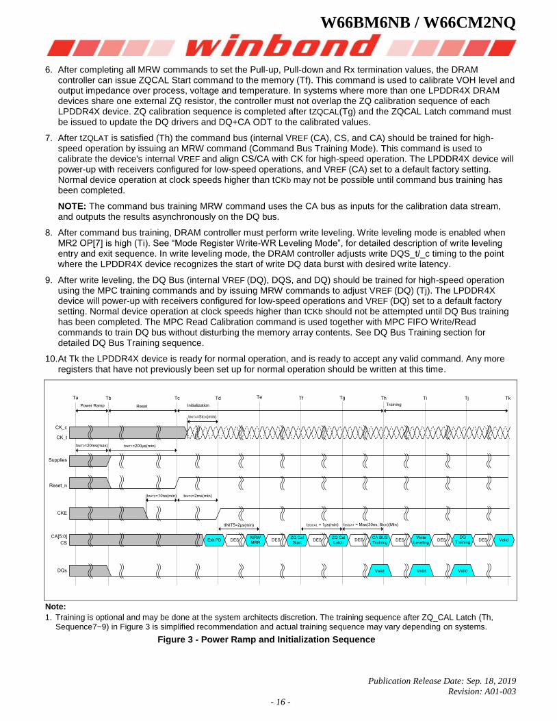
6. After completing all MRW commands to set the Pull-up, Pull-down and Rx termination values, the DRAM controller can issue ZQCAL Start command to the memory (Tf). This command is used to calibrate VOH level and output impedance over process, voltage and temperature. In systems where more than one LPDDR4X DRAM devices share one external ZQ resistor, the controller must not overlap the ZQ calibration sequence of each LPDDR4X device. ZQ calibration sequence is completed after tZQCAL(Tg) and the ZQCAL Latch command must be issued to update the DQ drivers and DQ+CA ODT to the calibrated values.
7. After tZQLAT is satisfied (Th) the command bus (internal VREF (CA), CS, and CA) should be trained for high-speed operation by issuing an MRW command (Command Bus Training Mode). This command is used to calibrate the device's internal VREF and align CS/CA with CK for high-speed operation. The LPDDR4X device will power-up with receivers configured for low-speed operations, and VREF (CA) set to a default factory setting. Normal device operation at clock speeds higher than tCKb may not be possible until command bus training has been completed.
NOTE: The command bus training MRW command uses the CA bus as inputs for the calibration data stream, and outputs the results asynchronously on the DQ bus.
8. After command bus training, DRAM controller must perform write leveling. Write leveling mode is enabled when MR2 OP[7] is high (Ti). See “Mode Register Write-WR Leveling Mode”, for detailed description of write leveling entry and exit sequence. In write leveling mode, the DRAM controller adjusts write DQS_t/_c timing to the point where the LPDDR4X device recognizes the start of write DQ data burst with desired write latency.
9. After write leveling, the DQ Bus (internal VREF (DQ), DQS, and DQ) should be trained for high-speed operation using the MPC training commands and by issuing MRW commands to adjust VREF (DQ) (Tj). The LPDDR4X device will power-up with receivers configured for low-speed operations and VREF (DQ) set to a default factory setting. Normal device operation at clock speeds higher than tCKb should not be attempted until DQ Bus training has been completed. The MPC Read Calibration command is used together with MPC FIFO Write/Read commands to train DQ bus without disturbing the memory array contents. See DQ Bus Training section for detailed DQ Bus Training sequence.
10. At Tk the LPDDR4X device is ready for normal operation, and is ready to accept any valid command. Any more registers that have not previously been set up for normal operation should be written at this time.
tINIT2=10ns(min) tINIT3=2ms(min)
tINIT5=2µs(min)
tINIT1=200µs(min)tINIT0=20ms(max)
tINIT4=5tCK(min)
InitializationResetPower Ramp Training
Ti Tj TkThTgTfTeTdTcTbTa
DQs
CS
CA[5:0]
CKE
Reset_n
Supplies
CK_c
CK_t
DES DES DES DES DES
tZQCAL = 1µs(min)
Exit PDMRW
MRR
ZQ Cal
Start
ZQ Cal
Latch
CA BUS
Training
Write
Leveling
DQ
TrainingDES DES Valid
ValidValid Valid
tZQLAT = Max(30ns, 8tCK)(Min)
Note:
1. Training is optional and may be done at the system architects discretion. The training sequence after ZQ_CAL Latch (Th, Sequence7~9) in Figure 3 is simplified recommendation and actual training sequence may vary depending on systems.
Figure 3 - Power Ramp and Initialization Sequence
W66BM6NB / W66CM2NQ
Publication Release Date: Sep. 18, 2019
Revision: A01-003
- 17 -
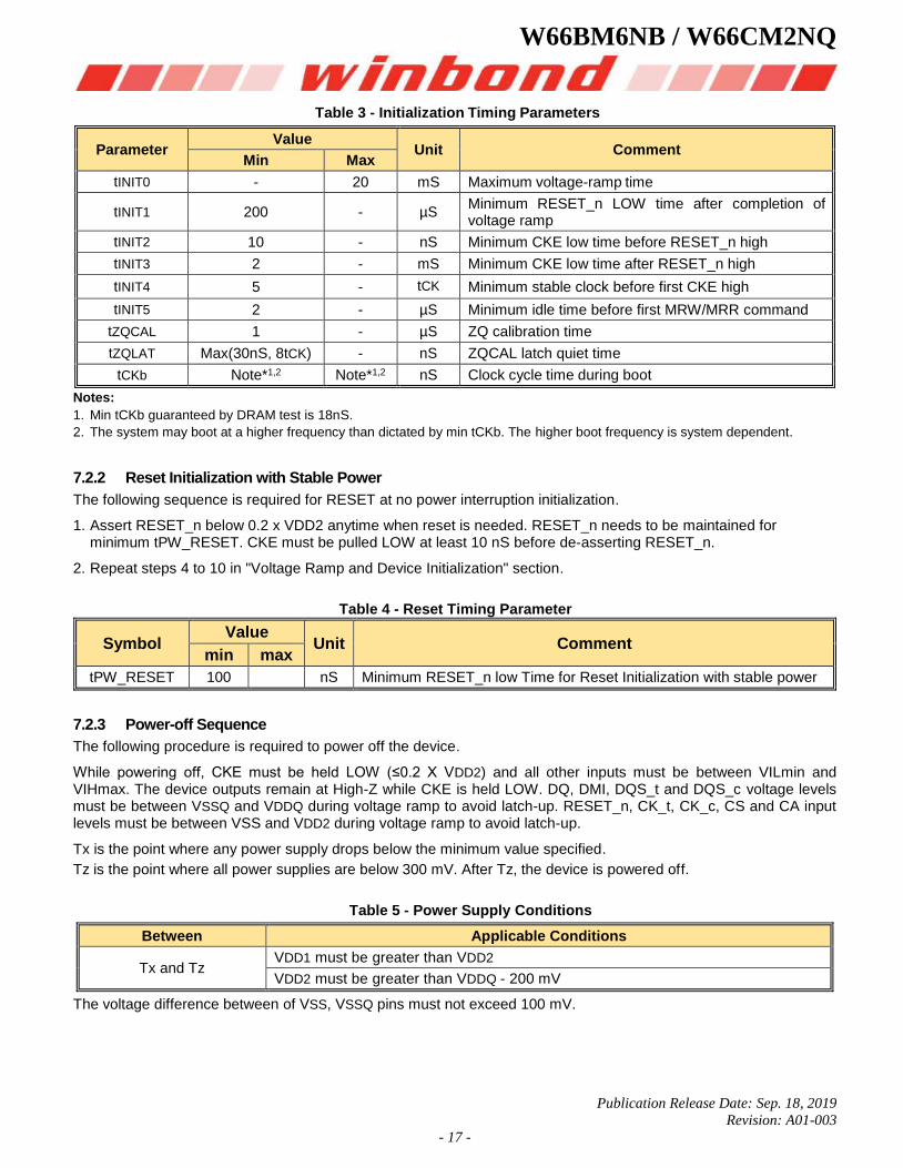
Table 3 - Initialization Timing Parameters
Parameter Value
Unit Comment Min Max
tINIT0 - 20 mS Maximum voltage-ramp time
tINIT1 200 - µS Minimum RESET_n LOW time after completion of voltage ramp
tINIT2 10 - nS Minimum CKE low time before RESET_n high
tINIT3 2 - mS Minimum CKE low time after RESET_n high
tINIT4 5 - tCK Minimum stable clock before first CKE high
tINIT5 2 - µS Minimum idle time before first MRW/MRR command
tZQCAL 1 - µS ZQ calibration time
tZQLAT Max(30nS, 8tCK) - nS ZQCAL latch quiet time
tCKb Note*1,2 Note*1,2 nS Clock cycle time during boot
Notes:
1. Min tCKb guaranteed by DRAM test is 18nS.
2. The system may boot at a higher frequency than dictated by min tCKb. The higher boot frequency is system dependent.
7.2.2 Reset Initialization with Stable Power
The following sequence is required for RESET at no power interruption initialization.
1. Assert RESET_n below 0.2 x VDD2 anytime when reset is needed. RESET_n needs to be maintained for minimum tPW_RESET. CKE must be pulled LOW at least 10 nS before de-asserting RESET_n.
2. Repeat steps 4 to 10 in "Voltage Ramp and Device Initialization" section.
Table 4 - Reset Timing Parameter
Symbol Value
Unit Comment min max
tPW_RESET 100 nS Minimum RESET_n low Time for Reset Initialization with stable power
7.2.3 Power-off Sequence
The following procedure is required to power off the device.
While powering off, CKE must be held LOW (≤0.2 X VDD2) and all other inputs must be between VILmin and VIHmax. The device outputs remain at High-Z while CKE is held LOW. DQ, DMI, DQS_t and DQS_c voltage levels must be between VSSQ and VDDQ during voltage ramp to avoid latch-up. RESET_n, CK_t, CK_c, CS and CA input levels must be between VSS and VDD2 during voltage ramp to avoid latch-up.
Tx is the point where any power supply drops below the minimum value specified.
Tz is the point where all power supplies are below 300 mV. After Tz, the device is powered off.
Table 5 - Power Supply Conditions
Between Applicable Conditions
Tx and Tz VDD1 must be greater than VDD2
VDD2 must be greater than VDDQ - 200 mV
The voltage difference between of VSS, VSSQ pins must not exceed 100 mV.
W66BM6NB / W66CM2NQ
Publication Release Date: Sep. 18, 2019
Revision: A01-003
- 18 -
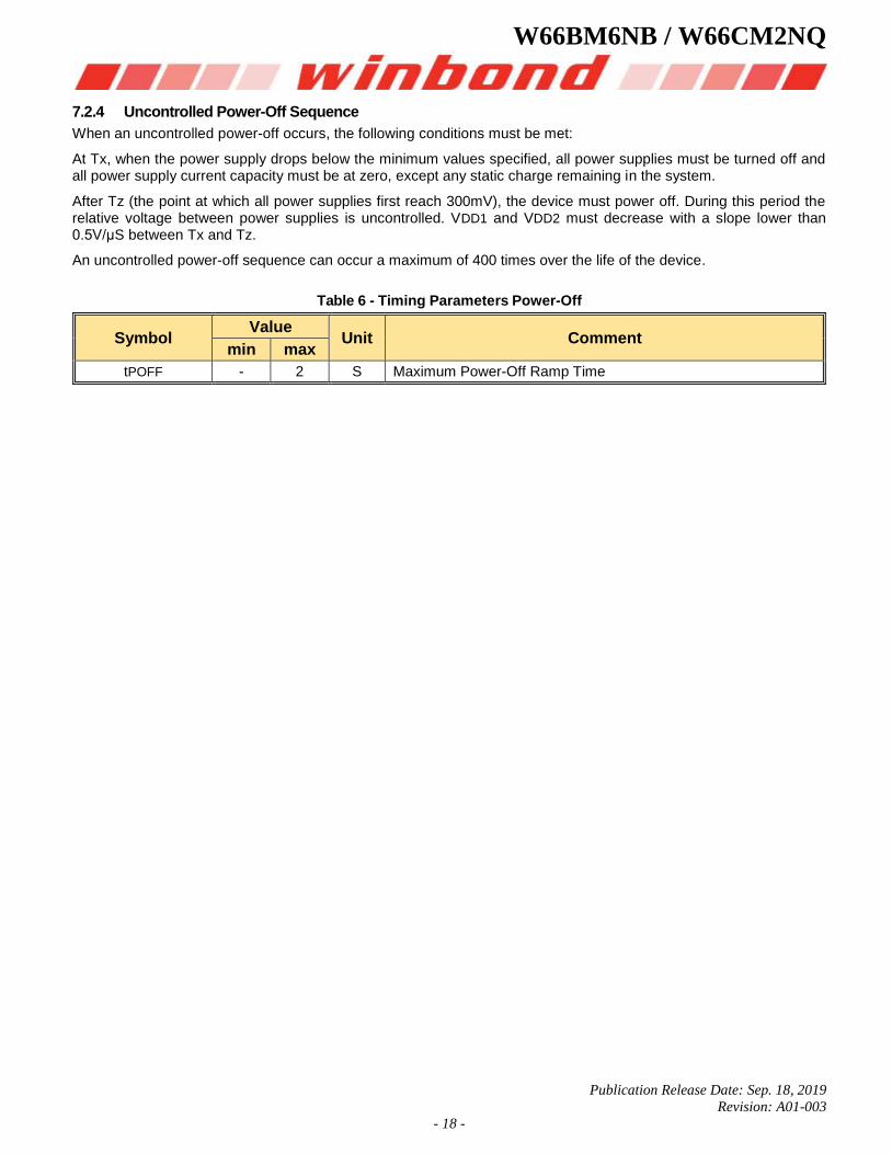
7.2.4 Uncontrolled Power-Off Sequence
When an uncontrolled power-off occurs, the following conditions must be met:
At Tx, when the power supply drops below the minimum values specified, all power supplies must be turned off and all power supply current capacity must be at zero, except any static charge remaining in the system.
After Tz (the point at which all power supplies first reach 300mV), the device must power off. During this period the relative voltage between power supplies is uncontrolled. VDD1 and VDD2 must decrease with a slope lower than 0.5V/μS between Tx and Tz.
An uncontrolled power-off sequence can occur a maximum of 400 times over the life of the device.
Table 6 - Timing Parameters Power-Off
Symbol Value
Unit Comment min max
tPOFF - 2 S Maximum Power-Off Ramp Time
W66BM6NB / W66CM2NQ
Publication Release Date: Sep. 18, 2019
Revision: A01-003
- 19 -
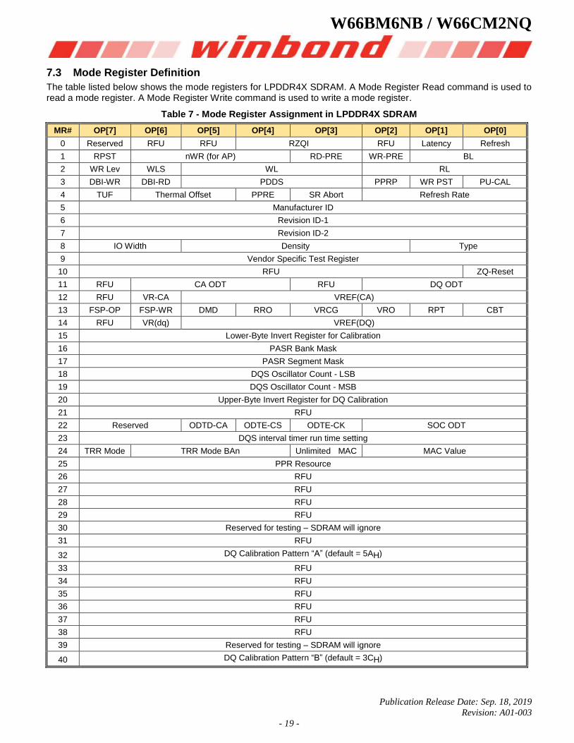
7.3 Mode Register Definition
The table listed below shows the mode registers for LPDDR4X SDRAM. A Mode Register Read command is used to read a mode register. A Mode Register Write command is used to write a mode register.
Table 7 - Mode Register Assignment in LPDDR4X SDRAM
MR# OP[7] OP[6] OP[5] OP[4] OP[3] OP[2] OP[1] OP[0]
0 Reserved RFU RFU RZQI RFU Latency Refresh
1 RPST nWR (for AP) RD-PRE WR-PRE BL
2 WR Lev WLS WL RL
3 DBI-WR DBI-RD PDDS PPRP WR PST PU-CAL
4 TUF Thermal Offset PPRE SR Abort Refresh Rate
5 Manufacturer ID
6 Revision ID-1
7 Revision ID-2
8 IO Width Density Type
9 Vendor Specific Test Register
10 RFU ZQ-Reset
11 RFU CA ODT RFU DQ ODT
12 RFU VR-CA VREF(CA)
13 FSP-OP FSP-WR DMD RRO VRCG VRO RPT CBT
14 RFU VR(dq) VREF(DQ)
15 Lower-Byte Invert Register for Calibration
16 PASR Bank Mask
17 PASR Segment Mask
18 DQS Oscillator Count - LSB
19 DQS Oscillator Count - MSB
20 Upper-Byte Invert Register for DQ Calibration
21 RFU
22 Reserved ODTD-CA ODTE-CS ODTE-CK SOC ODT
23 DQS interval timer run time setting
24 TRR Mode TRR Mode BAn Unlimited MAC MAC Value
25 PPR Resource
26 RFU
27 RFU
28 RFU
29 RFU
30 Reserved for testing – SDRAM will ignore
31 RFU
32 DQ Calibration Pattern “A” (default = 5AH)
33 RFU
34 RFU
35 RFU
36 RFU
37 RFU
38 RFU
39 Reserved for testing – SDRAM will ignore
40 DQ Calibration Pattern “B” (default = 3CH)
W66BM6NB / W66CM2NQ
Publication Release Date: Sep. 18, 2019
Revision: A01-003
- 20 -
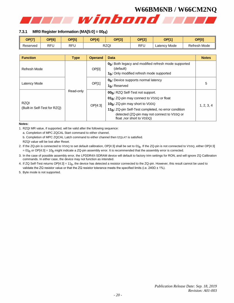
7.3.1 MR0 Register Information (MA[5:0] = 00H)
OP[7] OP[6] OP[5] OP[4] OP[3] OP[2] OP[1] OP[0]
Reserved RFU RFU RZQI RFU Latency Mode Refresh Mode
Function Type Operand Data Notes
Refresh Mode
Read-only
OP[0]
0b: Both legacy and modified refresh mode supported
(default)
1b: Only modified refresh mode supported
Latency Mode OP[1] 0b: Device supports normal latency
1b: Reserved 5
RZQI
(Built-in Self-Test for RZQ) OP[4:3]
00b: RZQ Self-Test not support.
01b: ZQ-pin may connect to VSSQ or float
10b: ZQ-pin may short to VDDQ
11b: ZQ-pin Self-Test completed, no error condition
detected (ZQ-pin may not connect to VSSQ or float ,nor short to VDDQ)
1, 2, 3, 4
Notes:
1. RZQI MR value, if supported, will be valid after the following sequence:
a. Completion of MPC ZQCAL Start command to either channel.
b. Completion of MPC ZQCAL Latch command to either channel then tZQLAT is satisfied.
RZQI value will be lost after Reset.
2. If the ZQ-pin is connected to VSSQ to set default calibration, OP[4:3] shall be set to 01b. If the ZQ-pin is not connected to VSSQ, either OP[4:3]
= 01b or OP[4:3] = 10b might indicate a ZQ-pin assembly error. It is recommended that the assembly error is corrected.
3. In the case of possible assembly error, the LPDDR4X-SDRAM device will default to factory trim settings for RON, and will ignore ZQ Calibration commands. In either case, the device may not function as intended.
4. If ZQ Self-Test returns OP[4:3] = 11b, the device has detected a resistor connected to the ZQ-pin. However, this result cannot be used to
validate the ZQ resistor value or that the ZQ resistor tolerance meets the specified limits (i.e. 240Ω ± 1%).
5. Byte mode is not supported.
W66BM6NB / W66CM2NQ
Publication Release Date: Sep. 18, 2019
Revision: A01-003
- 21 -
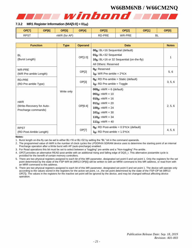
7.3.2 MR1 Register Information (MA[5:0] = 01H)
OP[7] OP[6] OP[5] OP[4] OP[3] OP[2] OP[1] OP[0]
RPST nWR (for AP) RD-PRE WR-PRE BL
Function Type Operand Data Notes
BL
(Burst Length)
Write only
OP[1:0]
00b: BL=16 Sequential (default)
01b: BL=32 Sequential
10b: BL=16 or 32 Sequential (on-the-fly)
All Others: Reserved
1
WR-PRE
(WR Pre-amble Length) OP[2]
0b: Reserved
1b: WR Pre-amble = 2*tCK 5, 6
RD-PRE
(RD Pre-amble Type) OP[3]
0b: RD Pre-amble = Static (default)
1b: RD Pre-amble = Toggle 3, 5, 6
nWR
(Write-Recovery for Auto-
Precharge commands)
OP[6:4]
000b: nWR = 6 (default)
001b: nWR = 10
010b: nWR = 16
011b: nWR = 20
100b: nWR = 24
101b: nWR = 30
110b: nWR = 34
111b: nWR = 40
2, 5, 6
RPST
(RD Post-Amble Length) OP[7]
0b: RD Post-amble = 0.5*tCK (default)
1b: RD Post-amble = 1.5*tCK 4, 5, 6
Notes:
1. Burst length on-the-fly can be set to either BL=16 or BL=32 by setting the “BL” bit in the command operands.
2. The programmed value of nWR is the number of clock cycles the LPDDR4X-SDRAM device uses to determine the starting point of an internal Precharge operation after a Write burst with AP (auto-precharge) enabled.
3. For Read operations this bit must be set to select between a "toggling" pre-amble and a "Non-toggling" Pre-amble.
4. OP[7] provides an alternative READ post-amble with an additional rising and falling edge of DQS_t. This alternative postamble cycle is provided for the benefit of certain memory controllers.
5. There are two physical registers assigned to each bit of this MR parameter, designated set point 0 and set point 1. Only the registers for the set point determined by the state of the FSP-WR bit (MR13 OP[6]) will be written to with an MRW command to this MR address, or read from with an MRR command to this address.
6. There are two physical registers assigned to each bit of this MR parameter, designated set point 0 and set point 1. The device will operate only according to the values stored in the registers for the active set point, i.e., the set point determined by the state of the FSP-OP bit (MR13 OP[7]). The values in the registers for the inactive set point will be ignored by the device, and may be changed without affecting device operation.
W66BM6NB / W66CM2NQ
Publication Release Date: Sep. 18, 2019
Revision: A01-003
- 22 -
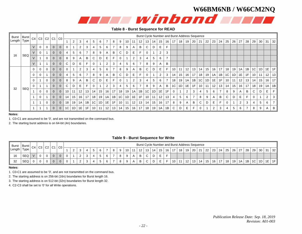
Table 8 - Burst Sequence for READ
Burst Length
Burst Type
C4 C3 C2 C1 C0 Burst Cycle Number and Burst Address Sequence
1 2 3 4 5 6 7 8 9 10 11 12 13 14 15 16 17 18 19 20 21 22 23 24 25 26 27 28 29 30 31 32
16 SEQ
V 0 0 0 0 0 1 2 3 4 5 6 7 8 9 A B C D E F
V 0 1 0 0 4 5 6 7 8 9 A B C D E F 0 1 2 3
V 1 0 0 0 8 9 A B C D E F 0 1 2 3 4 5 6 7
V 1 1 0 0 C D E F 0 1 2 3 4 5 6 7 8 9 A B
32 SEQ
0 0 0 0 0 0 1 2 3 4 5 6 7 8 9 A B C D E F 10 11 12 13 14 15 16 17 18 19 1A 1B 1C 1D 1E 1F
0 0 1 0 0 4 5 6 7 8 9 A B C D E F 0 1 2 3 14 15 16 17 18 19 1A 1B 1C 1D 1E 1F 10 11 12 13
0 1 0 0 0 8 9 A B C D E F 0 1 2 3 4 5 6 7 18 19 1A 1B 1C 1D 1E 1F 10 11 12 13 14 15 16 17
0 1 1 0 0 C D E F 0 1 2 3 4 5 6 7 8 9 A B 1C 1D 1E 1F 10 11 12 13 14 15 16 17 18 19 1A 1B
1 0 0 0 0 10 11 12 13 14 15 16 17 18 19 1A 1B 1C 1D 1E 1F 0 1 2 3 4 5 6 7 8 9 A B C D E F
1 0 1 0 0 14 15 16 17 18 19 1A 1B 1C 1D 1E 1F 10 11 12 13 4 5 6 7 8 9 A B C D E F 0 1 2 3
1 1 0 0 0 18 19 1A 1B 1C 1D 1E 1F 10 11 12 13 14 15 16 17 8 9 A B C D E F 0 1 2 3 4 5 6 7
1 1 1 0 0 1C 1D 1E 1F 10 11 12 13 14 15 16 17 18 19 1A 1B C D E F 0 1 2 3 4 5 6 7 8 9 A B
Notes:
1. C0-C1 are assumed to be '0', and are not transmitted on the command bus.
2. The starting burst address is on 64-bit (4n) boundaries.
Table 9 - Burst Sequence for Write
Burst Length
Burst Type
C4 C3 C2 C1 C0 Burst Cycle Number and Burst Address Sequence
1 2 3 4 5 6 7 8 9 10 11 12 13 14 15 16 17 18 19 20 21 22 23 24 25 26 27 28 29 30 31 32
16 SEQ V 0 0 0 0 0 1 2 3 4 5 6 7 8 9 A B C D E F
32 SEQ 0 0 0 0 0 0 1 2 3 4 5 6 7 8 9 A B C D E F 10 11 12 13 14 15 16 17 18 19 1A 1B 1C 1D 1E 1F
Notes:
1. C0-C1 are assumed to be '0', and are not transmitted on the command bus.
2. The starting address is on 256-bit (16n) boundaries for Burst length 16.
3. The starting address is on 512-bit (32n) boundaries for Burst length 32.
4. C2-C3 shall be set to '0' for all Write operations.
W66BM6NB / W66CM2NQ
Publication Release Date: Sep. 18, 2019
Revision: A01-003
- 23 -
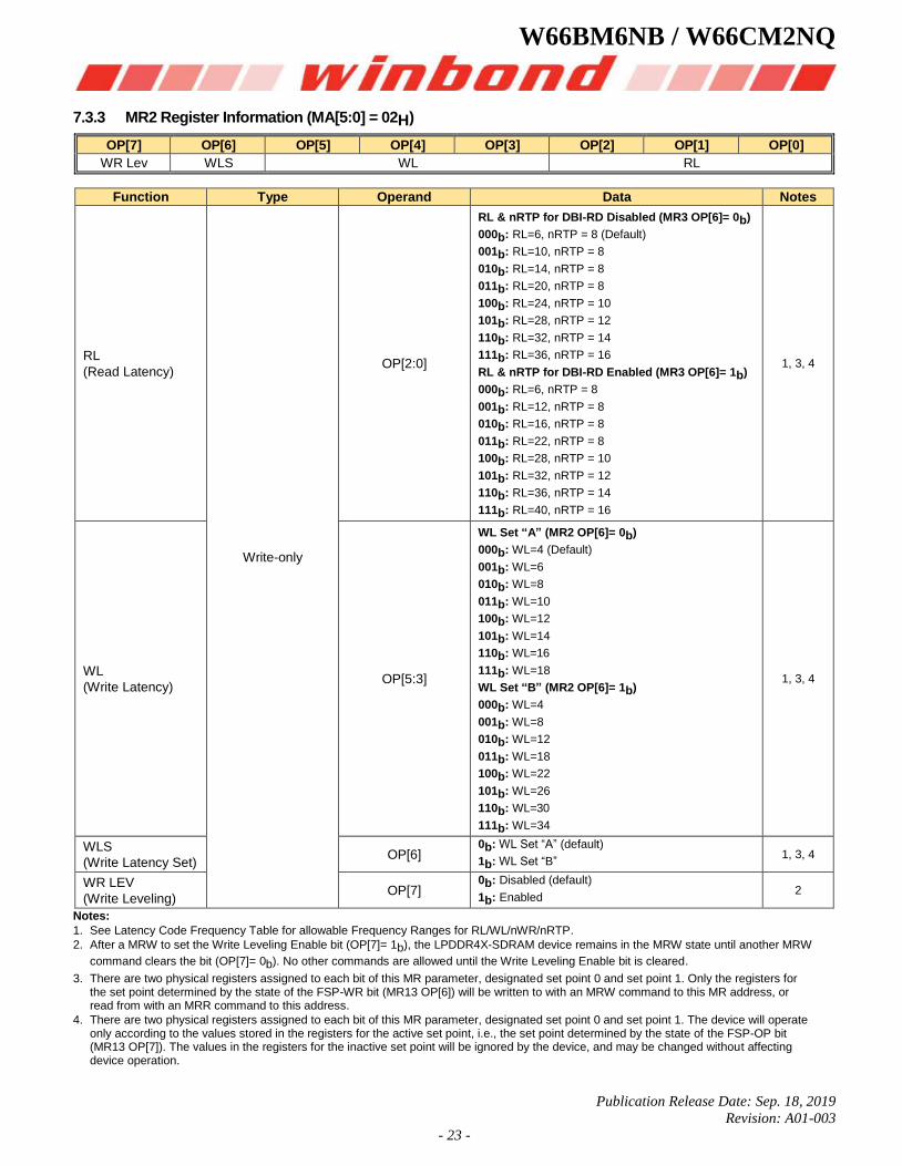
7.3.3 MR2 Register Information (MA[5:0] = 02H)
OP[7] OP[6] OP[5] OP[4] OP[3] OP[2] OP[1] OP[0]
WR Lev WLS WL RL
Function Type Operand Data Notes
RL
(Read Latency)
Write-only
OP[2:0]
RL & nRTP for DBI-RD Disabled (MR3 OP[6]= 0b)
000b: RL=6, nRTP = 8 (Default)
001b: RL=10, nRTP = 8
010b: RL=14, nRTP = 8
011b: RL=20, nRTP = 8
100b: RL=24, nRTP = 10
101b: RL=28, nRTP = 12
110b: RL=32, nRTP = 14
111b: RL=36, nRTP = 16
RL & nRTP for DBI-RD Enabled (MR3 OP[6]= 1b)
000b: RL=6, nRTP = 8
001b: RL=12, nRTP = 8
010b: RL=16, nRTP = 8
011b: RL=22, nRTP = 8
100b: RL=28, nRTP = 10
101b: RL=32, nRTP = 12
110b: RL=36, nRTP = 14
111b: RL=40, nRTP = 16
1, 3, 4
WL
(Write Latency) OP[5:3]
WL Set “A” (MR2 OP[6]= 0b)
000b: WL=4 (Default)
001b: WL=6
010b: WL=8
011b: WL=10
100b: WL=12
101b: WL=14
110b: WL=16
111b: WL=18
WL Set “B” (MR2 OP[6]= 1b)
000b: WL=4
001b: WL=8
010b: WL=12
011b: WL=18
100b: WL=22
101b: WL=26
110b: WL=30
111b: WL=34
1, 3, 4
WLS
(Write Latency Set) OP[6]
0b: WL Set “A” (default)
1b: WL Set “B” 1, 3, 4
WR LEV
(Write Leveling) OP[7]
0b: Disabled (default)
1b: Enabled 2
Notes:
1. See Latency Code Frequency Table for allowable Frequency Ranges for RL/WL/nWR/nRTP.
2. After a MRW to set the Write Leveling Enable bit (OP[7]= 1b), the LPDDR4X-SDRAM device remains in the MRW state until another MRW
command clears the bit (OP[7]= 0b). No other commands are allowed until the Write Leveling Enable bit is cleared.
3. There are two physical registers assigned to each bit of this MR parameter, designated set point 0 and set point 1. Only the registers for the set point determined by the state of the FSP-WR bit (MR13 OP[6]) will be written to with an MRW command to this MR address, or read from with an MRR command to this address.
4. There are two physical registers assigned to each bit of this MR parameter, designated set point 0 and set point 1. The device will operate only according to the values stored in the registers for the active set point, i.e., the set point determined by the state of the FSP-OP bit (MR13 OP[7]). The values in the registers for the inactive set point will be ignored by the device, and may be changed without affecting device operation.
W66BM6NB / W66CM2NQ
Publication Release Date: Sep. 18, 2019
Revision: A01-003
- 24 -
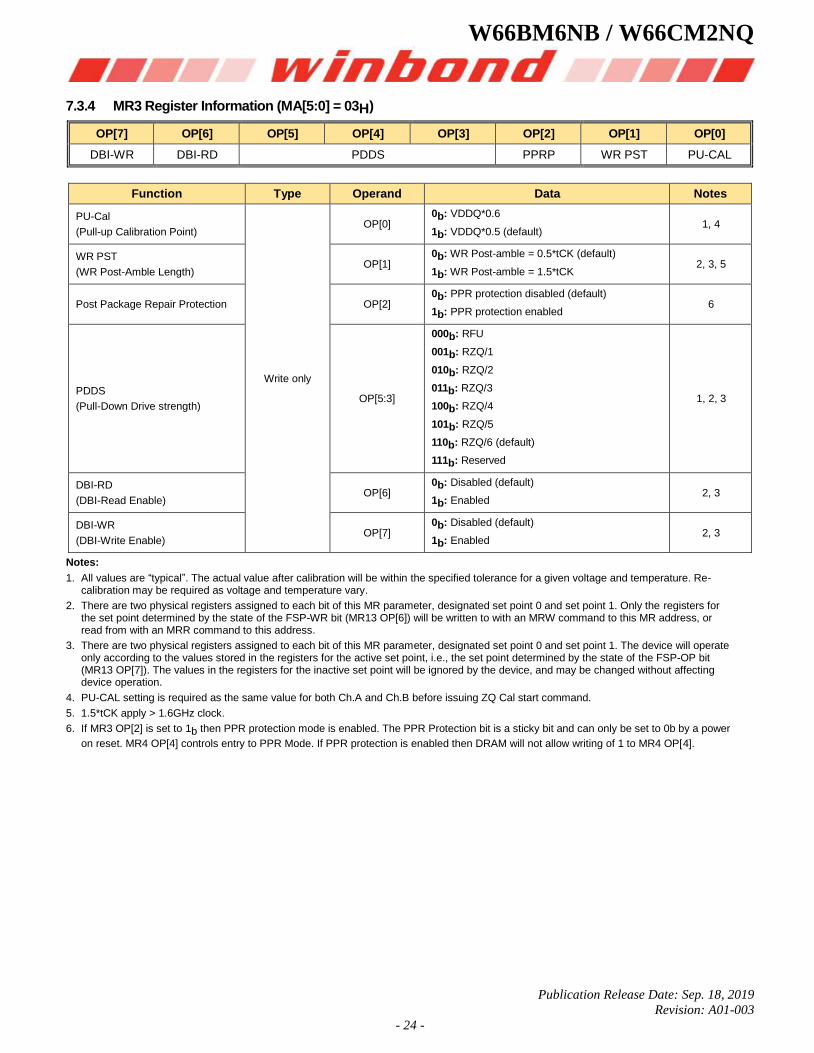
7.3.4 MR3 Register Information (MA[5:0] = 03H)
OP[7] OP[6] OP[5] OP[4] OP[3] OP[2] OP[1] OP[0]
DBI-WR DBI-RD PDDS PPRP WR PST PU-CAL
Function Type Operand Data Notes
PU-Cal
(Pull-up Calibration Point)
Write only
OP[0] 0b: VDDQ*0.6
1b: VDDQ*0.5 (default) 1, 4
WR PST
(WR Post-Amble Length) OP[1]
0b: WR Post-amble = 0.5*tCK (default)
1b: WR Post-amble = 1.5*tCK 2, 3, 5
Post Package Repair Protection OP[2] 0b: PPR protection disabled (default)
1b: PPR protection enabled 6
PDDS
(Pull-Down Drive strength) OP[5:3]
000b: RFU
001b: RZQ/1
010b: RZQ/2
011b: RZQ/3
100b: RZQ/4
101b: RZQ/5
110b: RZQ/6 (default)
111b: Reserved
1, 2, 3
DBI-RD
(DBI-Read Enable) OP[6]
0b: Disabled (default)
1b: Enabled 2, 3
DBI-WR
(DBI-Write Enable) OP[7]
0b: Disabled (default)
1b: Enabled 2, 3
Notes:
1. All values are “typical”. The actual value after calibration will be within the specified tolerance for a given voltage and temperature. Re-calibration may be required as voltage and temperature vary.
2. There are two physical registers assigned to each bit of this MR parameter, designated set point 0 and set point 1. Only the registers for the set point determined by the state of the FSP-WR bit (MR13 OP[6]) will be written to with an MRW command to this MR address, or read from with an MRR command to this address.
3. There are two physical registers assigned to each bit of this MR parameter, designated set point 0 and set point 1. The device will operate only according to the values stored in the registers for the active set point, i.e., the set point determined by the state of the FSP-OP bit (MR13 OP[7]). The values in the registers for the inactive set point will be ignored by the device, and may be changed without affecting device operation.
4. PU-CAL setting is required as the same value for both Ch.A and Ch.B before issuing ZQ Cal start command.
5. 1.5*tCK apply > 1.6GHz clock.
6. If MR3 OP[2] is set to 1b then PPR protection mode is enabled. The PPR Protection bit is a sticky bit and can only be set to 0b by a power
on reset. MR4 OP[4] controls entry to PPR Mode. If PPR protection is enabled then DRAM will not allow writing of 1 to MR4 OP[4].
W66BM6NB / W66CM2NQ
Publication Release Date: Sep. 18, 2019
Revision: A01-003
- 25 -
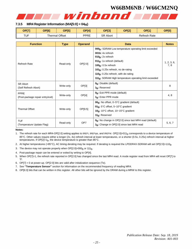
7.3.5 MR4 Register Information (MA[5:0] = 04H)
OP[7] OP[6] OP[5] OP[4] OP[3] OP[2] OP[1] OP[0]
TUF Thermal Offset PPRE SR Abort Refresh Rate
Function Type Operand Data Notes
Refresh Rate Read-only OP[2:0]
000b: SDRAM Low temperature operating limit exceeded
001b: 4x refresh
010b: 2x refresh
011b: 1x refresh (default)
100b: 0.5x refresh
101b: 0.25x refresh, no de-rating
110b: 0.25x refresh, with de-rating
111b: SDRAM High temperature operating limit exceeded
1, 2, 3, 6, 7, 8
SR Abort
(Self Refresh Abort) Write-only OP[3]
0b: Disable (default)
1b: Reserved 8
PPRE
(Post-package repair entry/exit) Write-only OP[4]
0b: Exit PPR mode (default)
1b: Enter PPR mode 4, 8
Thermal Offset Write-only OP[6:5]
00b: No offset, 0~5°C gradient (default)
01b: 5°C offset, 5~10°C gradient
10b: 10°C offset, 10~15°C gradient
11b: Reserved
TUF
(Temperature Update Flag) Read-only OP7
0b: No change in OP[2:0] since last MR4 read (default)
1b: Change in OP[2:0] since last MR4 read 5, 6, 7
Notes:
1. The refresh rate for each MR4-OP[2:0] setting applies to tREFI, tREFIpb, and tREFW. OP[2:0]=011b corresponds to a device temperature of
85°C. Other values require either a longer (2x, 4x) refresh interval at lower temperatures, or a shorter (0.5x, 0.25x) refresh interval at higher temperatures. If OP[2]=1b, the device temperature is greater than 85°C.
2. At higher temperatures (>85°C), AC timing derating may be required. If derating is required the LPDDR4X-SDRAM will set OP[2:0]=110b.
3. The device may not operate properly when OP[2:0]=000b or 111b.
4. Post-package repair can be entered or exited by writing to OP[4].
5. When OP[7]=1, the refresh rate reported in OP[2:0] has changed since the last MR4 read. A mode register read from MR4 will reset OP[7] to '0'.
6. OP[7] = 0 at power-up. OP[2:0] bits are valid after initialization sequence (Te).
7. See “Temperature Sensor” section for information on the recommended frequency of reading MR4.
8. OP[6:3] bits that can be written in this register. All other bits will be ignored by the DRAM during a MRW to this register.
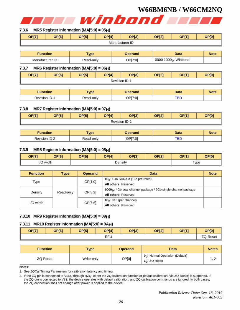
W66BM6NB / W66CM2NQ
Publication Release Date: Sep. 18, 2019
Revision: A01-003
- 26 -
7.3.6 MR5 Register Information (MA[5:0] = 05H)
OP[7] OP[6] OP[5] OP[4] OP[3] OP[2] OP[1] OP[0]
Manufacturer ID
Function Type Operand Data Note
Manufacturer ID Read-only OP[7:0] 0000 1000b: Winbond
7.3.7 MR6 Register Information (MA[5:0] = 06H)
OP[7] OP[6] OP[5] OP[4] OP[3] OP[2] OP[1] OP[0]
Revision ID-1
Function Type Operand Data Note
Revision ID-1 Read-only OP[7:0] TBD
7.3.8 MR7 Register Information (MA[5:0] = 07H)
OP[7] OP[6] OP[5] OP[4] OP[3] OP[2] OP[1] OP[0]
Revision ID-2
Function Type Operand Data Note
Revision ID-2 Read-only OP[7:0] TBD
7.3.9 MR8 Register Information (MA[5:0] = 08H)
OP[7] OP[6] OP[5] OP[4] OP[3] OP[2] OP[1] OP[0]
I/O width Density Type
Function Type Operand Data Note
Type
Read-only
OP[1:0] 00b: S16 SDRAM (16n pre-fetch)
All others: Reserved
Density OP[5:2] 0000b: 4Gb dual channel package / 2Gb single channel package
All others: Reserved
I/O width OP[7:6] 00b: x16 (per channel)
All others: Reserved
7.3.10 MR9 Register Information (MA[5:0] = 09H)
7.3.11 MR10 Register Information (MA[5:0] = 0AH)
OP[7] OP[6] OP[5] OP[4] OP[3] OP[2] OP[1] OP[0]
RFU ZQ-Reset
Function Type Operand Data Notes
ZQ-Reset Write-only OP[0] 0b: Normal Operation (Default)
1b: ZQ Reset 1, 2
Notes:
1. See ZQCal Timing Parameters for calibration latency and timing.
2. If the ZQ-pin is connected to VDDQ through RZQ, either the ZQ calibration function or default calibration (via ZQ-Reset) is supported. If the ZQ-pin is connected to VSS, the device operates with default calibration, and ZQ calibration commands are ignored. In both cases, the ZQ connection shall not change after power is applied to the device.
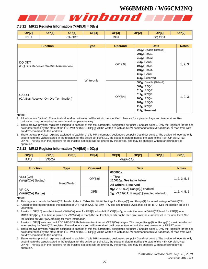
W66BM6NB / W66CM2NQ
Publication Release Date: Sep. 18, 2019
Revision: A01-003
- 27 -
7.3.12 MR11 Register Information (MA[5:0] = 0BH)
OP[7] OP[6] OP[5] OP[4] OP[3] OP[2] OP[1] OP[0]
RFU CA ODT RFU DQ ODT
Function Type Operand Data Notes
DQ ODT
(DQ Bus Receiver On-Die-Termination)
Write-only
OP[2:0]
000b: Disable (Default)
001b: RZQ/1
010b: RZQ/2
011b: RZQ/3
100b: RZQ/4
101b: RZQ/5
110b: RZQ/6
111b: Reserved
1, 2, 3
CA ODT
(CA Bus Receiver On-Die-Termination) OP[6:4]
000b: Disable (Default)
001b: RZQ/1
010b: RZQ/2
011b: RZQ/3
100b: RZQ/4
101b: RZQ/5
110b: RZQ/6
111b: Reserved
1, 2, 3
Notes:
1. All values are “typical”. The actual value after calibration will be within the specified tolerance for a given voltage and temperature. Re-calibration may be required as voltage and temperature vary.
2. There are two physical registers assigned to each bit of this MR parameter, designated set point 0 and set point 1. Only the registers for the set point determined by the state of the FSP-WR bit (MR13 OP[6]) will be written to with an MRW command to this MR address, or read from with an MRR command to this address.
3. There are two physical registers assigned to each bit of this MR parameter, designated set point 0 and set point 1. The device will operate only according to the values stored in the registers for the active set point, i.e., the set point determined by the state of the FSP-OP bit (MR13 OP[7]). The values in the registers for the inactive set point will be ignored by the device, and may be changed without affecting device operation.
7.3.13 MR12 Register Information (MA[5:0] = 0CH)
OP[7] OP[6] OP[5] OP[4] OP[3] OP[2] OP[1] OP[0]
RFU VR-CA VREF(CA)
Function Type Operand Data Notes
VREF(CA)
(VREF(CA) Setting) Read/Write
OP[5:0]
000000b:
-- Thru --
110010b: See table below
All Others: Reserved
1, 2, 3, 5, 6
VR-CA
(VREF(CA) Range) OP[6]
0b: VREF(CA) Range[0] enabled
1b: VREF(CA) Range[1] enabled (default) 1, 2, 4, 5, 6
Notes:
1. This register controls the VREF(CA) levels. Refer to Table 10 - VREF Settings for Range[0] and Range[1] for actual voltage of VREF(CA).
2. A read to this register places the contents of OP[7:0] on DQ[7:0]. Any RFU bits and unused DQ's shall be set to '0'. See the section on MRR Operation.
3. A write to OP[5:0] sets the internal VREF(CA) level for FSP[0] when MR13 OP[6]= 0b, or sets the internal VREF(CA)level for FSP[1] when
MR13 OP[6]=1b. The time required for VREF(CA) to reach the set level depends on the step size from the current level to the new level. See
the section on VREF(CA) training for more information.
4. A write to OP[6] switches the LPDDR4X-SDRAM between two internal VREF(CA) ranges. The range (Range[0] or Range[1]) must be selected when setting the VREF(CA) register. The value, once set, will be retained until over written, or until the next power-on or RESET event.
5. There are two physical registers assigned to each bit of this MR parameter, designated set point 0 and set point 1. Only the registers for the set point determined by the state of the FSP-WR bit (MR13 OP[6]) will be written to with an MRW command to this MR address, or read from with an MRR command to this address.
6. There are two physical registers assigned to each bit of this MR parameter, designated set point 0 and set point 1. The device will operate only according to the values stored in the registers for the active set point, i.e., the set point determined by the state of the FSP-OP bit (MR13 OP[7]). The values in the registers for the inactive set point will be ignored by the device, and may be changed without affecting device operation.

W66BM6NB / W66CM2NQ
Publication Release Date: Sep. 18, 2019
Revision: A01-003
- 28 -
Table 10 - VREF Settings for Range[0] and Range[1]
Function Operand Range[0] Values (% of VDDQ) Range[1] Values (% of VDDQ) Notes
VREF Settings for MR12
OP[5:0]
000000b: 15.0% 011010b: 30.5% 000000b: 32.9% 011010b: 48.5%
1, 2, 3
000001b: 15.6% 011011b: 31.1% 000001b: 33.5% 011011b: 49.1%
000010b: 16.2% 011100b: 31.7% 000010b: 34.1% 011100b: 49.7%
000011b: 16.8% 011101b: 32.3% 000011b: 34.7% 011101b: 50.3%
(Default)
000100b: 17.4% 011110b: 32.9% 000100b: 35.3% 011110b: 50.9%
000101b: 18.0% 011111b: 33.5% 000101b: 35.9% 011111b: 51.5%
000110b: 18.6% 100000b: 34.1% 000110b: 36.5% 100000b: 52.1%
000111b: 19.2% 100001b: 34.7% 000111b: 37.1% 100001b: 52.7%
001000b: 19.8% 100010b: 35.3% 001000b: 37.7% 100010b: 53.3%
001001b: 20.4% 100011b: 35.9% 001001b: 38.3% 100011b: 53.9%
001010b: 21.0% 100100b: 36.5% 001010b: 38.9% 100100b: 54.5%
001011b: 21.6% 100101b: 37.1% 001011b: 39.5% 100101b: 55.1%
001100b: 22.2% 100110b: 37.7% 001100b: 40.1% 100110b: 55.7%
001101b: 22.8% 100111b: 38.3% 001101b: 40.7% 100111b: 56.3%
001110b: 23.4% 101000b: 38.9% 001110b: 41.3% 101000b: 56.9%
001111b: 24.0% 101001b: 39.5% 001111b: 41.9% 101001b: 57.5%
010000b: 24.6% 101010b: 40.1% 010000b: 42.5% 101010b: 58.1%
010001b: 25.1% 101011b: 40.7% 010001b: 43.1% 101011b: 58.7%
010010b: 25.7% 101100b: 41.3% 010010b: 43.7% 101100b: 59.3%
010011b: 26.3% 101101b: 41.9% 010011b: 44.3% 101101b: 59.9%
010100b: 26.9% 101110b: 42.5% 010100b: 44.9% 101110b: 60.5%
010101b: 27.5% 101111b: 43.1% 010101b: 45.5% 101111b: 61.1%
010110b: 28.1% 110000b: 43.7% 010110b: 46.1% 110000b: 61.7%
010111b: 28.7% 110001b: 44.3% 010111b: 46.7% 110001b: 62.3%
011000b: 29.3% 110010b: 44.9% 011000b: 47.3% 110010b: 62.9%
011001b: 29.9% All Others: Reserved 011001b: 47.9% All Others: Reserved
Notes:
1. These values may be used for MR12 OP[5:0] to set the VREF(CA) levels in the LPDDR4X-SDRAM.
2. The range may be selected in the MR12 register by setting OP[6] appropriately.
3. The MR12 registers represents either FSP[0] or FSP[1]. Two frequency-set-points each for CA and DQ are provided to allow for faster switching between terminated and un-terminated operation, or between different high frequency setting which may use different terminations values.
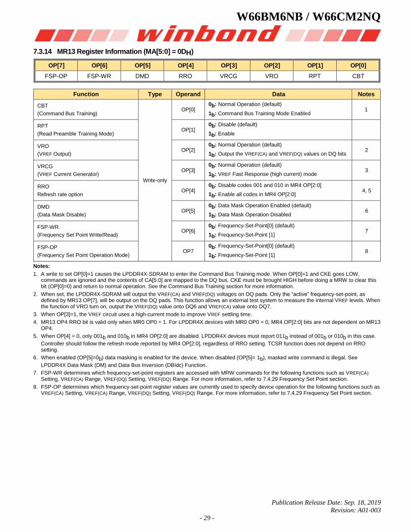
W66BM6NB / W66CM2NQ
Publication Release Date: Sep. 18, 2019
Revision: A01-003
- 29 -
7.3.14 MR13 Register Information (MA[5:0] = 0DH)
OP[7] OP[6] OP[5] OP[4] OP[3] OP[2] OP[1] OP[0]
FSP-OP FSP-WR DMD RRO VRCG VRO RPT CBT
Function Type Operand Data Notes
CBT
(Command Bus Training)
Write-only
OP[0] 0b: Normal Operation (default)
1b: Command Bus Training Mode Enabled 1
RPT
(Read Preamble Training Mode) OP[1]
0b: Disable (default)
1b: Enable
VRO
(VREF Output) OP[2]
0b: Normal Operation (default)
1b: Output the VREF(CA) and VREF(DQ) values on DQ bits 2
VRCG
(VREF Current Generator) OP[3]
0b: Normal Operation (default)
1b: VREF Fast Response (high current) mode 3
RRO
Refresh rate option OP[4]
0b: Disable codes 001 and 010 in MR4 OP[2:0]
1b: Enable all codes in MR4 OP[2:0] 4, 5
DMD
(Data Mask Disable) OP[5]
0b: Data Mask Operation Enabled (default)
1b: Data Mask Operation Disabled 6
FSP-WR
(Frequency Set Point Write/Read) OP[6]
0b: Frequency-Set-Point[0] (default)
1b: Frequency-Set-Point [1] 7
FSP-OP
(Frequency Set Point Operation Mode) OP7
0b: Frequency-Set-Point[0] (default)
1b: Frequency-Set-Point [1] 8
Notes:
1. A write to set OP[0]=1 causes the LPDDR4X-SDRAM to enter the Command Bus Training mode. When OP[0]=1 and CKE goes LOW, commands are ignored and the contents of CA[5:0] are mapped to the DQ bus. CKE must be brought HIGH before doing a MRW to clear this bit (OP[0]=0) and return to normal operation. See the Command Bus Training section for more information.
2. When set, the LPDDR4X-SDRAM will output the VREF(CA) and VREF(DQ) voltages on DQ pads. Only the “active” frequency-set-point, as defined by MR13 OP[7], will be output on the DQ pads. This function allows an external test system to measure the internal VREF levels. When the function of VRO turn on, output the VREF(DQ) value onto DQ6 and VREF(CA) value onto DQ7.
3. When OP[3]=1, the VREF circuit uses a high-current mode to improve VREF settling time.
4. MR13 OP4 RRO bit is valid only when MR0 OP0 = 1. For LPDDR4X devices with MR0 OP0 = 0, MR4 OP[2:0] bits are not dependent on MR13 OP4.
5. When OP[4] = 0, only 001b and 010b in MR4 OP[2:0] are disabled. LPDDR4X devices must report 011b instead of 001b or 010b in this case.
Controller should follow the refresh mode reported by MR4 OP[2:0], regardless of RRO setting. TCSR function does not depend on RRO setting.
6. When enabled (OP[5]=0b) data masking is enabled for the device. When disabled (OP[5]= 1b), masked write command is illegal. See
LPDDR4X Data Mask (DM) and Data Bus Inversion (DBIdc) Function.
7. FSP-WR determines which frequency-set-point registers are accessed with MRW commands for the following functions such as VREF(CA) Setting, VREF(CA) Range, VREF(DQ) Setting, VREF(DQ) Range. For more information, refer to 7.4.29 Frequency Set Point section.
8. FSP-OP determines which frequency-set-point register values are currently used to specify device operation for the following functions such as VREF(CA) Setting, VREF(CA) Range, VREF(DQ) Setting, VREF(DQ) Range. For more information, refer to 7.4.29 Frequency Set Point section.
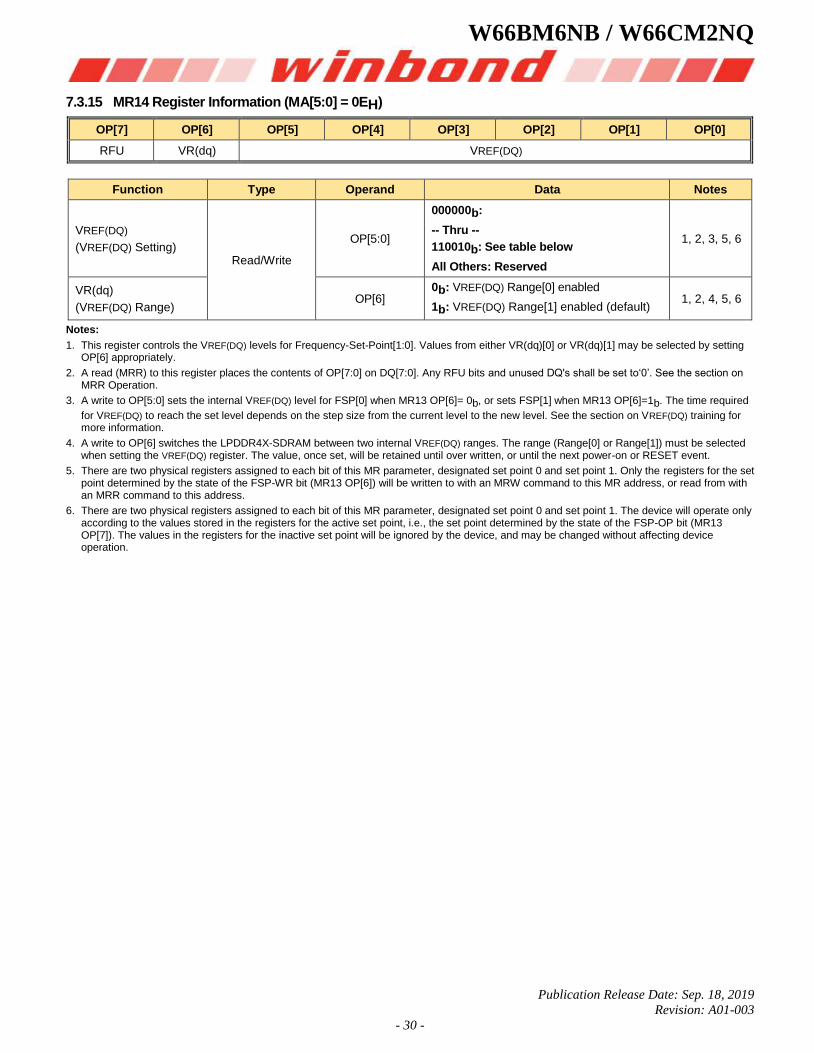
W66BM6NB / W66CM2NQ
Publication Release Date: Sep. 18, 2019
Revision: A01-003
- 30 -
7.3.15 MR14 Register Information (MA[5:0] = 0EH)
OP[7] OP[6] OP[5] OP[4] OP[3] OP[2] OP[1] OP[0]
RFU VR(dq) VREF(DQ)
Function Type Operand Data Notes
VREF(DQ)
(VREF(DQ) Setting) Read/Write
OP[5:0]
000000b:
-- Thru --
110010b: See table below
All Others: Reserved
1, 2, 3, 5, 6
VR(dq)
(VREF(DQ) Range) OP[6]
0b: VREF(DQ) Range[0] enabled
1b: VREF(DQ) Range[1] enabled (default) 1, 2, 4, 5, 6
Notes:
1. This register controls the VREF(DQ) levels for Frequency-Set-Point[1:0]. Values from either VR(dq)[0] or VR(dq)[1] may be selected by setting OP[6] appropriately.
2. A read (MRR) to this register places the contents of OP[7:0] on DQ[7:0]. Any RFU bits and unused DQ's shall be set to‘0’. See the section on MRR Operation.
3. A write to OP[5:0] sets the internal VREF(DQ) level for FSP[0] when MR13 OP[6]= 0b, or sets FSP[1] when MR13 OP[6]=1b. The time required
for VREF(DQ) to reach the set level depends on the step size from the current level to the new level. See the section on VREF(DQ) training for more information.
4. A write to OP[6] switches the LPDDR4X-SDRAM between two internal VREF(DQ) ranges. The range (Range[0] or Range[1]) must be selected when setting the VREF(DQ) register. The value, once set, will be retained until over written, or until the next power-on or RESET event.
5. There are two physical registers assigned to each bit of this MR parameter, designated set point 0 and set point 1. Only the registers for the set point determined by the state of the FSP-WR bit (MR13 OP[6]) will be written to with an MRW command to this MR address, or read from with an MRR command to this address.
6. There are two physical registers assigned to each bit of this MR parameter, designated set point 0 and set point 1. The device will operate only according to the values stored in the registers for the active set point, i.e., the set point determined by the state of the FSP-OP bit (MR13 OP[7]). The values in the registers for the inactive set point will be ignored by the device, and may be changed without affecting device operation.
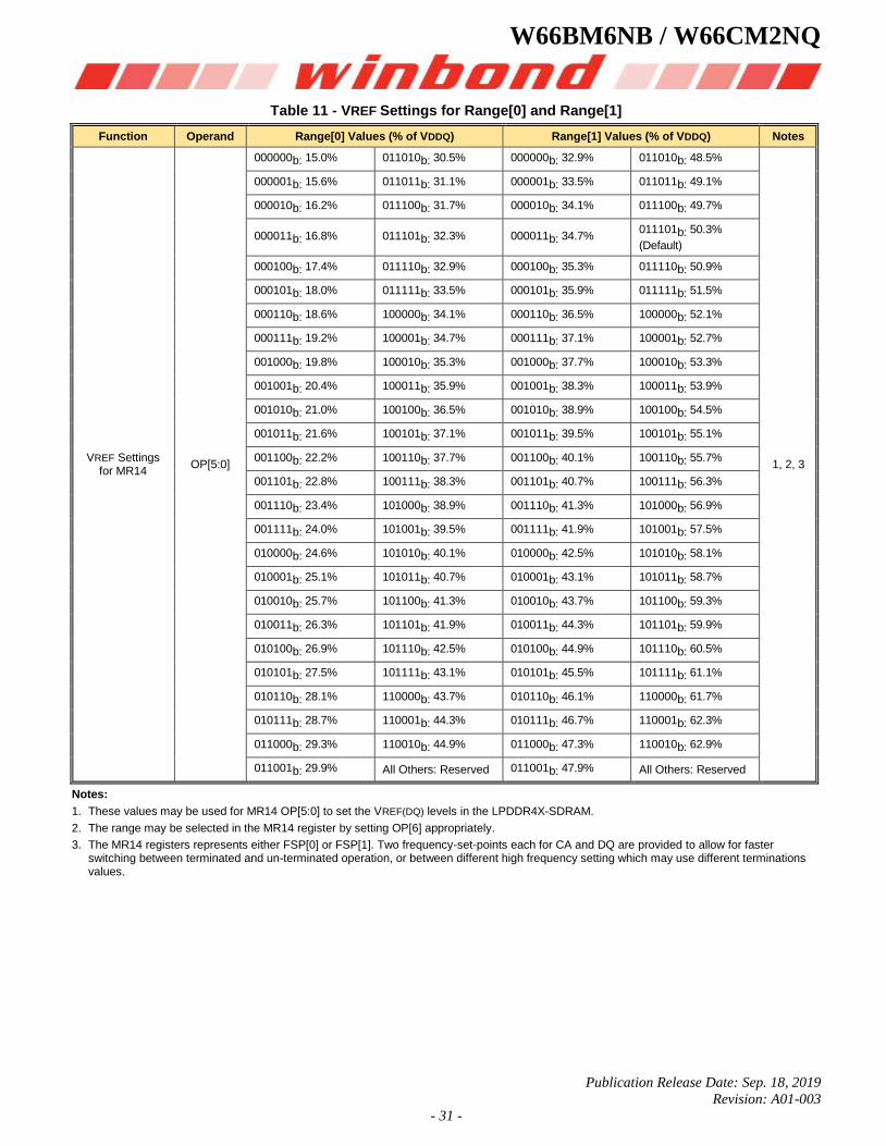
W66BM6NB / W66CM2NQ
Publication Release Date: Sep. 18, 2019
Revision: A01-003
- 31 -
Table 11 - VREF Settings for Range[0] and Range[1]
Function Operand Range[0] Values (% of VDDQ) Range[1] Values (% of VDDQ) Notes
VREF Settings for MR14
OP[5:0]
000000b: 15.0% 011010b: 30.5% 000000b: 32.9% 011010b: 48.5%
1, 2, 3
000001b: 15.6% 011011b: 31.1% 000001b: 33.5% 011011b: 49.1%
000010b: 16.2% 011100b: 31.7% 000010b: 34.1% 011100b: 49.7%
000011b: 16.8% 011101b: 32.3% 000011b: 34.7% 011101b: 50.3%
(Default)
000100b: 17.4% 011110b: 32.9% 000100b: 35.3% 011110b: 50.9%
000101b: 18.0% 011111b: 33.5% 000101b: 35.9% 011111b: 51.5%
000110b: 18.6% 100000b: 34.1% 000110b: 36.5% 100000b: 52.1%
000111b: 19.2% 100001b: 34.7% 000111b: 37.1% 100001b: 52.7%
001000b: 19.8% 100010b: 35.3% 001000b: 37.7% 100010b: 53.3%
001001b: 20.4% 100011b: 35.9% 001001b: 38.3% 100011b: 53.9%
001010b: 21.0% 100100b: 36.5% 001010b: 38.9% 100100b: 54.5%
001011b: 21.6% 100101b: 37.1% 001011b: 39.5% 100101b: 55.1%
001100b: 22.2% 100110b: 37.7% 001100b: 40.1% 100110b: 55.7%
001101b: 22.8% 100111b: 38.3% 001101b: 40.7% 100111b: 56.3%
001110b: 23.4% 101000b: 38.9% 001110b: 41.3% 101000b: 56.9%
001111b: 24.0% 101001b: 39.5% 001111b: 41.9% 101001b: 57.5%
010000b: 24.6% 101010b: 40.1% 010000b: 42.5% 101010b: 58.1%
010001b: 25.1% 101011b: 40.7% 010001b: 43.1% 101011b: 58.7%
010010b: 25.7% 101100b: 41.3% 010010b: 43.7% 101100b: 59.3%
010011b: 26.3% 101101b: 41.9% 010011b: 44.3% 101101b: 59.9%
010100b: 26.9% 101110b: 42.5% 010100b: 44.9% 101110b: 60.5%
010101b: 27.5% 101111b: 43.1% 010101b: 45.5% 101111b: 61.1%
010110b: 28.1% 110000b: 43.7% 010110b: 46.1% 110000b: 61.7%
010111b: 28.7% 110001b: 44.3% 010111b: 46.7% 110001b: 62.3%
011000b: 29.3% 110010b: 44.9% 011000b: 47.3% 110010b: 62.9%
011001b: 29.9% All Others: Reserved 011001b: 47.9% All Others: Reserved
Notes:
1. These values may be used for MR14 OP[5:0] to set the VREF(DQ) levels in the LPDDR4X-SDRAM.
2. The range may be selected in the MR14 register by setting OP[6] appropriately.
3. The MR14 registers represents either FSP[0] or FSP[1]. Two frequency-set-points each for CA and DQ are provided to allow for faster switching between terminated and un-terminated operation, or between different high frequency setting which may use different terminations values.
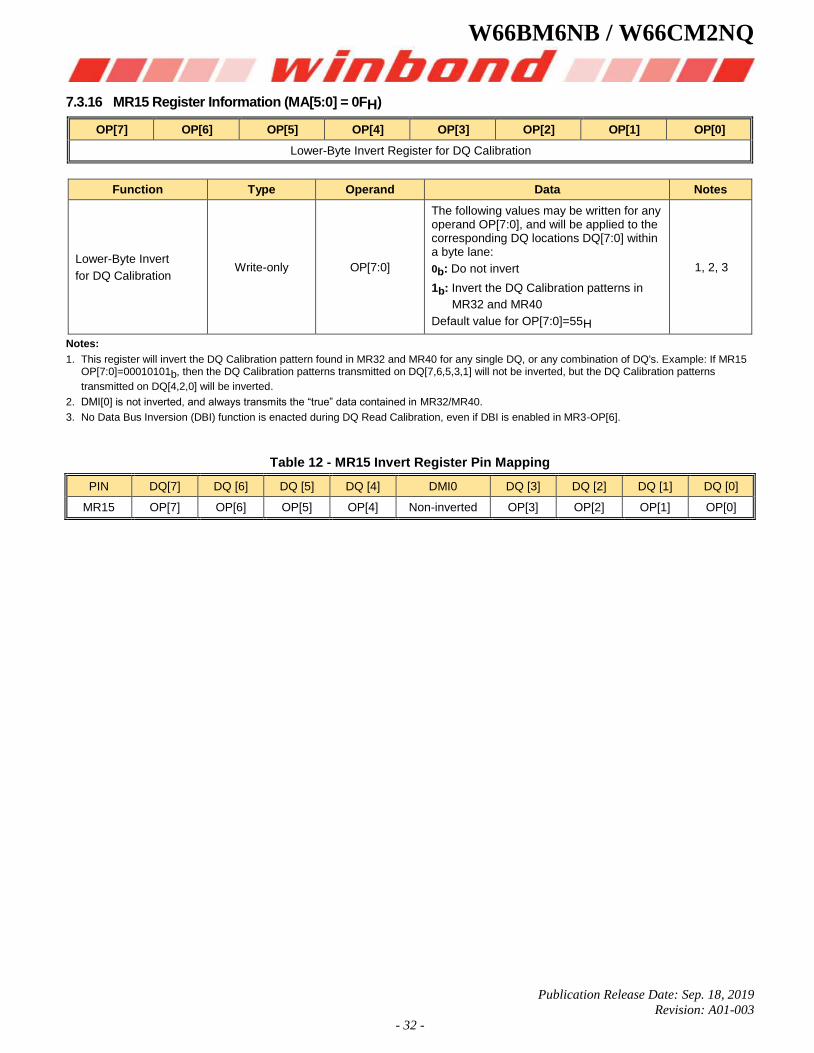
W66BM6NB / W66CM2NQ
Publication Release Date: Sep. 18, 2019
Revision: A01-003
- 32 -
7.3.16 MR15 Register Information (MA[5:0] = 0FH)
OP[7] OP[6] OP[5] OP[4] OP[3] OP[2] OP[1] OP[0]
Lower-Byte Invert Register for DQ Calibration
Function Type Operand Data Notes
Lower-Byte Invert
for DQ Calibration Write-only OP[7:0]
The following values may be written for any operand OP[7:0], and will be applied to the corresponding DQ locations DQ[7:0] within a byte lane:
0b: Do not invert
1b: Invert the DQ Calibration patterns in
MR32 and MR40
Default value for OP[7:0]=55H
1, 2, 3
Notes:
1. This register will invert the DQ Calibration pattern found in MR32 and MR40 for any single DQ, or any combination of DQ's. Example: If MR15 OP[7:0]=00010101b, then the DQ Calibration patterns transmitted on DQ[7,6,5,3,1] will not be inverted, but the DQ Calibration patterns
transmitted on DQ[4,2,0] will be inverted.
2. DMI[0] is not inverted, and always transmits the “true” data contained in MR32/MR40.
3. No Data Bus Inversion (DBI) function is enacted during DQ Read Calibration, even if DBI is enabled in MR3-OP[6].
Table 12 - MR15 Invert Register Pin Mapping
PIN DQ[7] DQ [6] DQ [5] DQ [4] DMI0 DQ [3] DQ [2] DQ [1] DQ [0]
MR15 OP[7] OP[6] OP[5] OP[4] Non-inverted OP[3] OP[2] OP[1] OP[0]
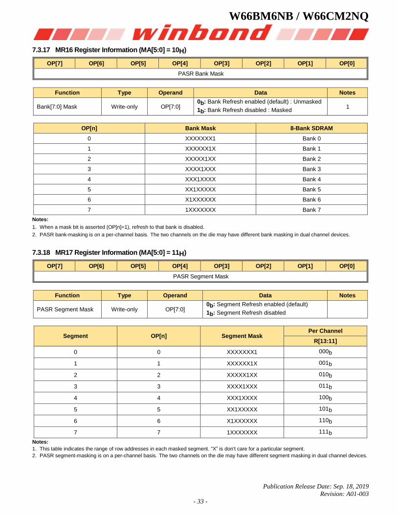
W66BM6NB / W66CM2NQ
Publication Release Date: Sep. 18, 2019
Revision: A01-003
- 33 -
7.3.17 MR16 Register Information (MA[5:0] = 10H)
OP[7] OP[6] OP[5] OP[4] OP[3] OP[2] OP[1] OP[0]
PASR Bank Mask
Function Type Operand Data Notes
Bank[7:0] Mask Write-only OP[7:0] 0b: Bank Refresh enabled (default) : Unmasked
1b: Bank Refresh disabled : Masked 1
OP[n] Bank Mask 8-Bank SDRAM
0 XXXXXXX1 Bank 0
1 XXXXXX1X Bank 1
2 XXXXX1XX Bank 2
3 XXXX1XXX Bank 3
4 XXX1XXXX Bank 4
5 XX1XXXXX Bank 5
6 X1XXXXXX Bank 6
7 1XXXXXXX Bank 7
Notes:
1. When a mask bit is asserted (OP[n]=1), refresh to that bank is disabled.
2. PASR bank-masking is on a per-channel basis. The two channels on the die may have different bank masking in dual channel devices.
7.3.18 MR17 Register Information (MA[5:0] = 11H)
OP[7] OP[6] OP[5] OP[4] OP[3] OP[2] OP[1] OP[0]
PASR Segment Mask
Function Type Operand Data Notes
PASR Segment Mask Write-only OP[7:0] 0b: Segment Refresh enabled (default)
1b: Segment Refresh disabled
Segment OP[n] Segment Mask Per Channel
R[13:11]
0 0 XXXXXXX1 000b
1 1 XXXXXX1X 001b
2 2 XXXXX1XX 010b
3 3 XXXX1XXX 011b
4 4 XXX1XXXX 100b
5 5 XX1XXXXX 101b
6 6 X1XXXXXX 110b
7 7 1XXXXXXX 111b
Notes:
1. This table indicates the range of row addresses in each masked segment. “X” is don't care for a particular segment.
2. PASR segment-masking is on a per-channel basis. The two channels on the die may have different segment masking in dual channel devices.
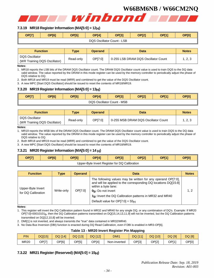
W66BM6NB / W66CM2NQ
Publication Release Date: Sep. 18, 2019
Revision: A01-003
- 34 -
7.3.19 MR18 Register Information (MA[5:0] = 12H)
OP[7] OP[6] OP[5] OP[4] OP[3] OP[2] OP[1] OP[0]
DQS Oscillator Count - LSB
Function Type Operand Data Notes
DQS Oscillator
(WR Training DQS Oscillator) Read-only OP[7:0] 0-255 LSB DRAM DQS Oscillator Count 1, 2, 3
Notes:
1. MR18 reports the LSB bits of the DRAM DQS Oscillator count. The DRAM DQS Oscillator count value is used to train DQS to the DQ data valid window. The value reported by the DRAM in this mode register can be used by the memory controller to periodically adjust the phase of DQS relative to DQ.
2. Both MR18 and MR19 must be read (MRR) and combined to get the value of the DQS Oscillator count.
3. A new MPC [Start DQS Oscillator] should be issued to reset the contents of MR18/MR19.
7.3.20 MR19 Register Information (MA[5:0] = 13H)
OP[7] OP[6] OP[5] OP[4] OP[3] OP[2] OP[1] OP[0]
DQS Oscillator Count - MSB
Function Type Operand Data Notes
DQS Oscillator
(WR Training DQS Oscillator) Read-only OP[7:0] 0-255 MSB DRAM DQS Oscillator Count 1, 2, 3
Notes:
1. MR19 reports the MSB bits of the DRAM DQS Oscillator count. The DRAM DQS Oscillator count value is used to train DQS to the DQ data valid window. The value reported by the DRAM in this mode register can be used by the memory controller to periodically adjust the phase of DQS relative to DQ.
2. Both MR18 and MR19 must be read (MRR) and combined to get the value of the DQS Oscillator count.
3. A new MPC [Start DQS Oscillator] should be issued to reset the contents of MR18/MR19.
7.3.21 MR20 Register Information (MA[5:0] = 14 H)
OP[7] OP[6] OP[5] OP[4] OP[3] OP[2] OP[1] OP[0]
Upper-Byte Invert Register for DQ Calibration
Function Type Operand Data Notes
Upper-Byte Invert
for DQ Calibration Write-only OP[7:0]
The following values may be written for any operand OP[7:0], and will be applied to the corresponding DQ locations DQ[15:8] within a byte lane:
0b: Do not invert
1b: Invert the DQ Calibration patterns in MR32 and MR40
Default value for OP[7:0] = 55H
1, 2
Notes:
1. This register will invert the DQ Calibration pattern found in MR32 and MR40 for any single DQ, or any combination of DQ's. Example: If MR20 OP[7:0]=00010101b, then the DQ Calibration patterns transmitted on DQ[15,14,13,11,9] will not be inverted, but the DQ Calibration patterns
transmitted on DQ[12,10,8] will be inverted.
2. DMI[1] is not inverted, and always transmits the "true" data contained in MR32/MR40.
3. No Data Bus Inversion (DBI) function is enacted during DQ Read Calibration, even if DBI is enabled in MR3-OP[6].
Table 13 - MR20 Invert Register Pin Mapping
PIN DQ[15] DQ [14] DQ [13] DQ [12] DMI1 DQ [11] DQ [10] DQ [9] DQ [8]
MR20 OP[7] OP[6] OP[5] OP[4] Non-inverted OP[3] OP[2] OP[1] OP[0]
7.3.22 MR21 Register (Reserved) (MA[5:0] = 15H)
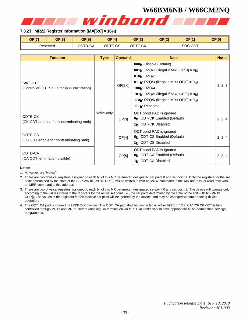
W66BM6NB / W66CM2NQ
Publication Release Date: Sep. 18, 2019
Revision: A01-003
- 35 -
7.3.23 MR22 Register Information (MA[5:0] = 16H)
OP[7] OP[6] OP[5] OP[4] OP[3] OP[2] OP[1] OP[0]
Reserved ODTD-CA ODTE-CS ODTE-CK SOC ODT
Function Type Operand Data Notes
SoC ODT
(Controller ODT Value for VOH calibration)
Write-only
OP[2:0]
000b: Disable (Default)
001b: RZQ/1 (illegal if MR3 OP[0] = 0b)
010b: RZQ/2
011b: RZQ/3 (illegal if MR3 OP[0] = 0b)
100b: RZQ/4
101b: RZQ/5 (illegal if MR3 OP[0] = 0b)
110b: RZQ/6 (illegal if MR3 OP[0] = 0b)
111b: Reserved
1, 2, 3
ODTE-CK
(CK ODT enabled for nonterminating rank) OP[3]
ODT bond PAD is ignored
0b: ODT-CK Enabled (Default)
1b: ODT-CK Disabled
2, 3, 4
ODTE-CS
(CS ODT enable for nonterminating rank) OP[4]
ODT bond PAD is ignored
0b: ODT-CS Enabled (Default)
1b: ODT-CS Disabled
2, 3, 4
ODTD-CA
(CA ODT termination disable) OP[5]
ODT bond PAD is ignored
0b: ODT-CA Enabled (Default)
1b: ODT-CA Disabled
2, 3, 4
Notes:
1. All values are “typical”.
2. There are two physical registers assigned to each bit of this MR parameter, designated set point 0 and set point 1. Only the registers for the set point determined by the state of the FSP-WR bit (MR13 OP[6]) will be written to with an MRW command to this MR address, or read from with an MRR command to this address.
3. There are two physical registers assigned to each bit of this MR parameter, designated set point 0 and set point 1. The device will operate only according to the values stored in the registers for the active set point, i.e., the set point determined by the state of the FSP-OP bit (MR13 OP[7]). The values in the registers for the inactive set point will be ignored by the device, and may be changed without affecting device operation.
4. The ODT_CA pad is ignored by LPDDR4X devices. The ODT_CA pad shall be connected to either VDD2 or VSS. CA/ CS/ CK ODT is fully controlled through MR11 and MR22. Before enabling CA termination via MR11, all ranks should have appropriate MR22 termination settings programmed.
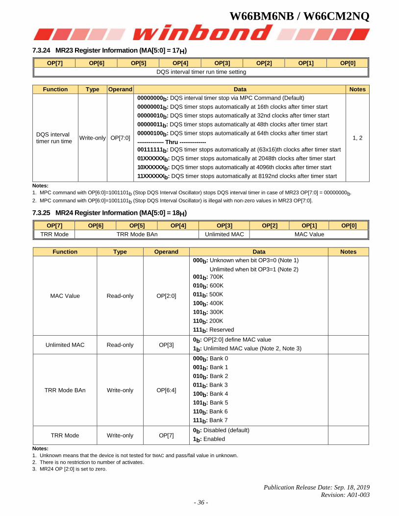
W66BM6NB / W66CM2NQ
Publication Release Date: Sep. 18, 2019
Revision: A01-003
- 36 -
7.3.24 MR23 Register Information (MA[5:0] = 17H)
OP[7] OP[6] OP[5] OP[4] OP[3] OP[2] OP[1] OP[0]
DQS interval timer run time setting
Function Type Operand Data Notes
DQS interval timer run time
Write-only OP[7:0]
00000000b: DQS interval timer stop via MPC Command (Default)
00000001b: DQS timer stops automatically at 16th clocks after timer start
00000010b: DQS timer stops automatically at 32nd clocks after timer start
00000011b: DQS timer stops automatically at 48th clocks after timer start
00000100b: DQS timer stops automatically at 64th clocks after timer start
-------------- Thru --------------
00111111b: DQS timer stops automatically at (63x16)th clocks after timer start
01XXXXXXb: DQS timer stops automatically at 2048th clocks after timer start
10XXXXXXb: DQS timer stops automatically at 4096th clocks after timer start
11XXXXXXb: DQS timer stops automatically at 8192nd clocks after timer start
1, 2
Notes:
1. MPC command with OP[6:0]=1001101b (Stop DQS Interval Oscillator) stops DQS interval timer in case of MR23 OP[7:0] = 00000000b.
2. MPC command with OP[6:0]=1001101b (Stop DQS Interval Oscillator) is illegal with non-zero values in MR23 OP[7:0].
7.3.25 MR24 Register Information (MA[5:0] = 18H)
OP[7] OP[6] OP[5] OP[4] OP[3] OP[2] OP[1] OP[0]
TRR Mode TRR Mode BAn Unlimited MAC MAC Value
Function Type Operand Data Notes
MAC Value Read-only OP[2:0]
000b: Unknown when bit OP3=0 (Note 1)
Unlimited when bit OP3=1 (Note 2)
001b: 700K
010b: 600K
011b: 500K
100b: 400K
101b: 300K
110b: 200K
111b: Reserved
Unlimited MAC Read-only OP[3] 0b: OP[2:0] define MAC value
1b: Unlimited MAC value (Note 2, Note 3)
TRR Mode BAn Write-only OP[6:4]
000b: Bank 0
001b: Bank 1
010b: Bank 2
011b: Bank 3
100b: Bank 4
101b: Bank 5
110b: Bank 6
111b: Bank 7
TRR Mode Write-only OP[7] 0b: Disabled (default)
1b: Enabled
Notes:
1. Unknown means that the device is not tested for tMAC and pass/fail value in unknown.
2. There is no restriction to number of activates.
3. MR24 OP [2:0] is set to zero.
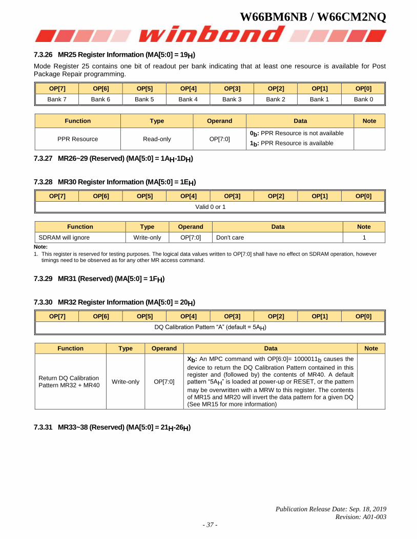
W66BM6NB / W66CM2NQ
Publication Release Date: Sep. 18, 2019
Revision: A01-003
- 37 -
7.3.26 MR25 Register Information (MA[5:0] = 19H)
Mode Register 25 contains one bit of readout per bank indicating that at least one resource is available for Post Package Repair programming.
OP[7] OP[6] OP[5] OP[4] OP[3] OP[2] OP[1] OP[0]
Bank 7 Bank 6 Bank 5 Bank 4 Bank 3 Bank 2 Bank 1 Bank 0
Function Type Operand Data Note
PPR Resource Read-only OP[7:0] 0b: PPR Resource is not available
1b: PPR Resource is available
7.3.27 MR26~29 (Reserved) (MA[5:0] = 1AH-1DH)
7.3.28 MR30 Register Information (MA[5:0] = 1EH)
OP[7] OP[6] OP[5] OP[4] OP[3] OP[2] OP[1] OP[0]
Valid 0 or 1
Function Type Operand Data Note
SDRAM will ignore Write-only OP[7:0] Don't care 1
Note:
1. This register is reserved for testing purposes. The logical data values written to OP[7:0] shall have no effect on SDRAM operation, however timings need to be observed as for any other MR access command.
7.3.29 MR31 (Reserved) (MA[5:0] = 1FH)
7.3.30 MR32 Register Information (MA[5:0] = 20H)
OP[7] OP[6] OP[5] OP[4] OP[3] OP[2] OP[1] OP[0]
DQ Calibration Pattern “A” (default = 5AH)
Function Type Operand Data Note
Return DQ Calibration Pattern MR32 + MR40
Write-only OP[7:0]
Xb: An MPC command with OP[6:0]= 1000011b causes the
device to return the DQ Calibration Pattern contained in this register and (followed by) the contents of MR40. A default pattern “5AH” is loaded at power-up or RESET, or the pattern
may be overwritten with a MRW to this register. The contents of MR15 and MR20 will invert the data pattern for a given DQ (See MR15 for more information)
7.3.31 MR33~38 (Reserved) (MA[5:0] = 21H-26H)
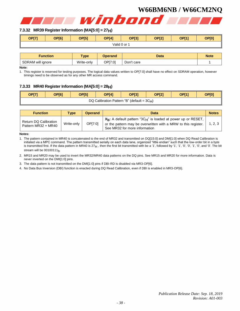
W66BM6NB / W66CM2NQ
Publication Release Date: Sep. 18, 2019
Revision: A01-003
- 38 -
7.3.32 MR39 Register Information (MA[5:0] = 27H)
OP[7] OP[6] OP[5] OP[4] OP[3] OP[2] OP[1] OP[0]
Valid 0 or 1
Function Type Operand Data Note
SDRAM will ignore Write-only OP[7:0] Don't care 1
Note:
1. This register is reserved for testing purposes. The logical data values written to OP[7:0] shall have no effect on SDRAM operation, however timings need to be observed as for any other MR access command.
7.3.33 MR40 Register Information (MA[5:0] = 28H)
OP[7] OP[6] OP[5] OP[4] OP[3] OP[2] OP[1] OP[0]
DQ Calibration Pattern “B” (default = 3CH)
Function Type Operand Data Notes
Return DQ Calibration Pattern MR32 + MR40
Write-only OP[7:0]
Xb: A default pattern “3CH” is loaded at power up or RESET,
or the pattern may be overwritten with a MRW to this register. See MR32 for more information
1, 2, 3
Notes:
1. The pattern contained in MR40 is concatenated to the end of MR32 and transmitted on DQ[15:0] and DMI[1:0] when DQ Read Calibration is initiated via a MPC command. The pattern transmitted serially on each data lane, organized “little endian” such that the low-order bit in a byte is transmitted first. If the data pattern in MR40 is 27H , then the first bit transmitted with be a '1', followed by '1', '1', '0', '0', '1', '0', and '0'. The bit
stream will be 00100111b.
2. MR15 and MR20 may be used to invert the MR32/MR40 data patterns on the DQ pins. See MR15 and MR20 for more information. Data is never inverted on the DMI[1:0] pins.
3. The data pattern is not transmitted on the DMI[1:0] pins if DBI-RD is disabled via MR3-OP[6].
4. No Data Bus Inversion (DBI) function is enacted during DQ Read Calibration, even if DBI is enabled in MR3-OP[6].
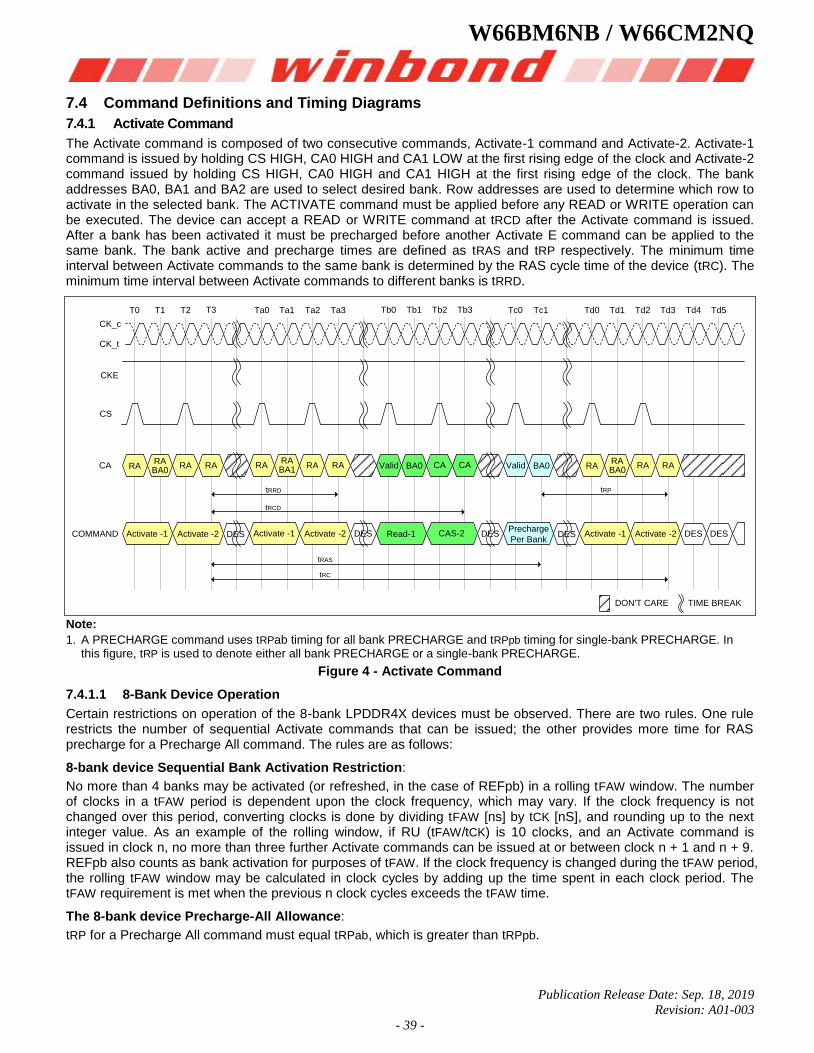
W66BM6NB / W66CM2NQ
Publication Release Date: Sep. 18, 2019
Revision: A01-003
- 39 -
7.4 Command Definitions and Timing Diagrams
7.4.1 Activate Command
The Activate command is composed of two consecutive commands, Activate-1 command and Activate-2. Activate-1 command is issued by holding CS HIGH, CA0 HIGH and CA1 LOW at the first rising edge of the clock and Activate-2 command issued by holding CS HIGH, CA0 HIGH and CA1 HIGH at the first rising edge of the clock. The bank addresses BA0, BA1 and BA2 are used to select desired bank. Row addresses are used to determine which row to activate in the selected bank. The ACTIVATE command must be applied before any READ or WRITE operation can be executed. The device can accept a READ or WRITE command at tRCD after the Activate command is issued. After a bank has been activated it must be precharged before another Activate E command can be applied to the same bank. The bank active and precharge times are defined as tRAS and tRP respectively. The minimum time interval between Activate commands to the same bank is determined by the RAS cycle time of the device (tRC). The minimum time interval between Activate commands to different banks is tRRD.
CK_c
CK_t
CKE
CS
CA
COMMAND
T0
tRAS
tRRD
tRCD
tRC
tRP
T1 T2 T3 Ta0 Ta1 Ta2 Ta3 Tb0 Tb1 Tb2 Tb3 Td0 Td1 Td2 Td3 Td4 Td5Tc0 Tc1
RA RA RABA0RA RA RA RA
BA1RA
Valid CA CABA0 Valid BA0 RA RA RABA0RA
Activate -1 Activate -2 DES Activate -1 Activate -2 Activate -1 Activate -2DES DES DES DES DESRead-1 CAS-2Precharge
Per Bank
TIME BREAKDON'T CARE
Note:
1. A PRECHARGE command uses tRPab timing for all bank PRECHARGE and tRPpb timing for single-bank PRECHARGE. In this figure, tRP is used to denote either all bank PRECHARGE or a single-bank PRECHARGE.
Figure 4 - Activate Command
7.4.1.1 8-Bank Device Operation
Certain restrictions on operation of the 8-bank LPDDR4X devices must be observed. There are two rules. One rule restricts the number of sequential Activate commands that can be issued; the other provides more time for RAS precharge for a Precharge All command. The rules are as follows:
8-bank device Sequential Bank Activation Restriction:
No more than 4 banks may be activated (or refreshed, in the case of REFpb) in a rolling tFAW window. The number of clocks in a tFAW period is dependent upon the clock frequency, which may vary. If the clock frequency is not changed over this period, converting clocks is done by dividing tFAW [ns] by tCK [nS], and rounding up to the next integer value. As an example of the rolling window, if RU (tFAW/tCK) is 10 clocks, and an Activate command is issued in clock n, no more than three further Activate commands can be issued at or between clock n + 1 and n + 9. REFpb also counts as bank activation for purposes of tFAW. If the clock frequency is changed during the tFAW period, the rolling tFAW window may be calculated in clock cycles by adding up the time spent in each clock period. The tFAW requirement is met when the previous n clock cycles exceeds the tFAW time.
The 8-bank device Precharge-All Allowance:
tRP for a Precharge All command must equal tRPab, which is greater than tRPpb.
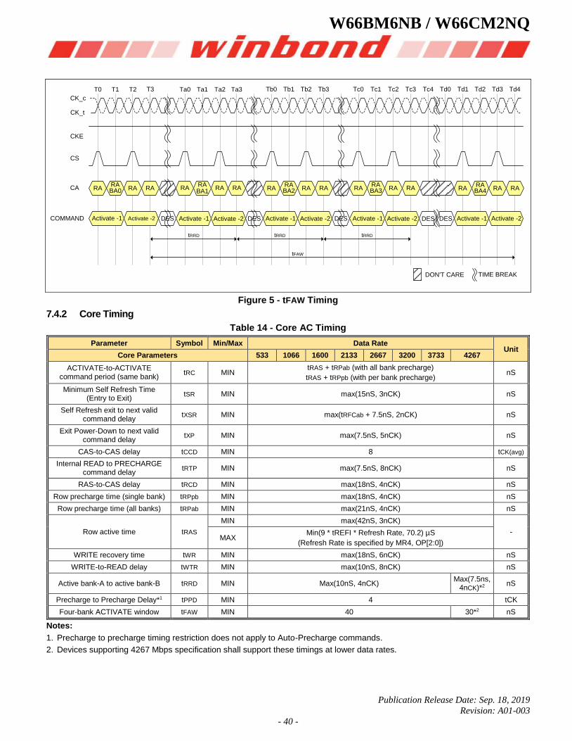
W66BM6NB / W66CM2NQ
Publication Release Date: Sep. 18, 2019
Revision: A01-003
- 40 -
tRRD tRRD tRRD
tFAW
TIME BREAKDON'T CARE
CK_c
CK_t
CKE
CS
CA
COMMAND
RA RA RABA0RA
RA RA RABA1RA
RA RA RABA2RA
RA RA RABA3RA
RA RA RABA4RA
Activate -1 Activate -2 Activate -1 Activate -2 Activate -1 Activate -2 Activate -1 Activate -2 Activate -1 Activate -2DES DES DES DES DES
T0 T1 T2 T3 Ta0 Ta1 Ta2 Ta3 Tb0 Tb1 Tb2 Tb3 Tc0 Tc1 Tc2 Tc3 Td0 Td1 Td2 Td3 Td4Tc4
Figure 5 - tFAW Timing
7.4.2 Core Timing
Table 14 - Core AC Timing
Parameter Symbol Min/Max Data Rate Unit
Core Parameters 533 1066 1600 2133 2667 3200 3733 4267
ACTIVATE-to-ACTIVATE command period (same bank)
tRC MIN tRAS + tRPab (with all bank precharge)
tRAS + tRPpb (with per bank precharge) nS
Minimum Self Refresh Time (Entry to Exit)
tSR MIN max(15nS, 3nCK) nS
Self Refresh exit to next valid command delay
tXSR MIN max(tRFCab + 7.5nS, 2nCK) nS
Exit Power-Down to next valid command delay
tXP MIN max(7.5nS, 5nCK) nS
CAS-to-CAS delay tCCD MIN 8 tCK(avg)
Internal READ to PRECHARGE command delay
tRTP MIN max(7.5nS, 8nCK) nS
RAS-to-CAS delay tRCD MIN max(18nS, 4nCK) nS
Row precharge time (single bank) tRPpb MIN max(18nS, 4nCK) nS
Row precharge time (all banks) tRPab MIN max(21nS, 4nCK) nS
Row active time tRAS
MIN max(42nS, 3nCK)
- MAX
Min(9 * tREFI * Refresh Rate, 70.2) µS
(Refresh Rate is specified by MR4, OP[2:0])
WRITE recovery time tWR MIN max(18nS, 6nCK) nS
WRITE-to-READ delay tWTR MIN max(10nS, 8nCK) nS
Active bank-A to active bank-B tRRD MIN Max(10nS, 4nCK) Max(7.5ns,
4nCK)*2 nS
Precharge to Precharge Delay*1 tPPD MIN 4 tCK
Four-bank ACTIVATE window tFAW MIN 40 30*2 nS
Notes:
1. Precharge to precharge timing restriction does not apply to Auto-Precharge commands.
2. Devices supporting 4267 Mbps specification shall support these timings at lower data rates.
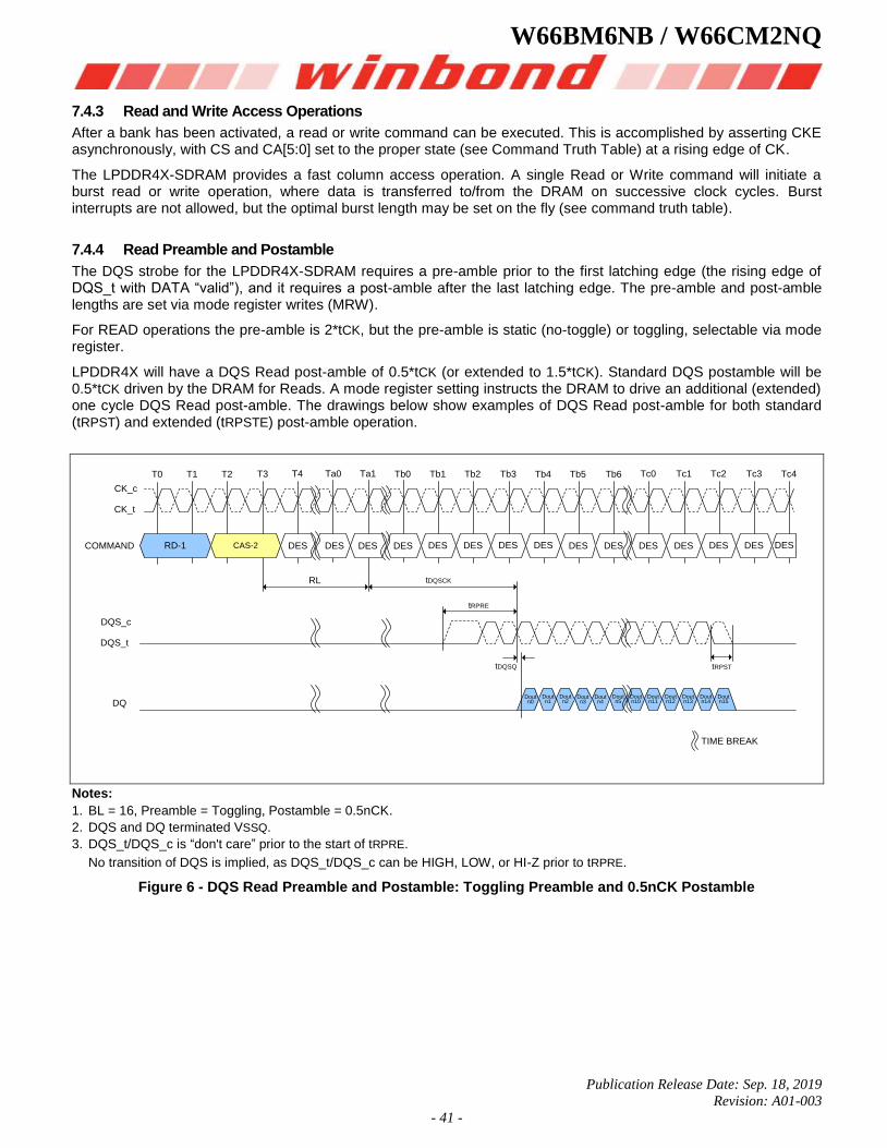
W66BM6NB / W66CM2NQ
Publication Release Date: Sep. 18, 2019
Revision: A01-003
- 41 -
7.4.3 Read and Write Access Operations
After a bank has been activated, a read or write command can be executed. This is accomplished by asserting CKE asynchronously, with CS and CA[5:0] set to the proper state (see Command Truth Table) at a rising edge of CK.
The LPDDR4X-SDRAM provides a fast column access operation. A single Read or Write command will initiate a burst read or write operation, where data is transferred to/from the DRAM on successive clock cycles. Burst interrupts are not allowed, but the optimal burst length may be set on the fly (see command truth table).
7.4.4 Read Preamble and Postamble
The DQS strobe for the LPDDR4X-SDRAM requires a pre-amble prior to the first latching edge (the rising edge of DQS_t with DATA “valid”), and it requires a post-amble after the last latching edge. The pre-amble and post-amble lengths are set via mode register writes (MRW).
For READ operations the pre-amble is 2*tCK, but the pre-amble is static (no-toggle) or toggling, selectable via mode register.
LPDDR4X will have a DQS Read post-amble of 0.5*tCK (or extended to 1.5*tCK). Standard DQS postamble will be 0.5*tCK driven by the DRAM for Reads. A mode register setting instructs the DRAM to drive an additional (extended) one cycle DQS Read post-amble. The drawings below show examples of DQS Read post-amble for both standard (tRPST) and extended (tRPSTE) post-amble operation.
TIME BREAK
CK_c
CK_t
COMMAND
DQS_c
DQS_t
DQ
T0 T1 T2 T3 T4 Ta0 Ta1 Tb0 Tb1 Tb2 Tb3 Tb4 Tb5 Tb6 Tc0 Tc1 Tc2 Tc3 Tc4
RL tDQSCK
tRPRE
tRPSTtDQSQ
DES DES DES DES DES DES DES DES DES DES DES DES DES DES DES
Dout n0
Dout n1
Dout n2
Dout n3
Dout n4
Dout n5
Dout n10
Dout n11
Dout n12
Dout n13
Dout n14
Dout n15
RD-1 CAS-2
Notes:
1. BL = 16, Preamble = Toggling, Postamble = 0.5nCK.
2. DQS and DQ terminated VSSQ.
3. DQS_t/DQS_c is “don't care” prior to the start of tRPRE.
No transition of DQS is implied, as DQS_t/DQS_c can be HIGH, LOW, or HI-Z prior to tRPRE.
Figure 6 - DQS Read Preamble and Postamble: Toggling Preamble and 0.5nCK Postamble
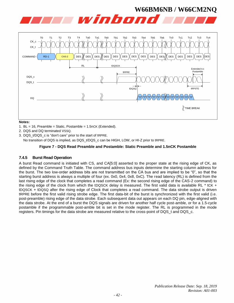
W66BM6NB / W66CM2NQ
Publication Release Date: Sep. 18, 2019
Revision: A01-003
- 42 -
TIME BREAK
CK_c
CK_t
COMMAND
DQS_c
DQS_t
DQ
T0 T1 T2 T3 T4 Ta0 Ta1 Tb0 Tb1 Tb2 Tb3 Tb4 Tb5 Tb6 Tc0 Tc1 Tc2 Tc3 Tc4
RL tDQSCK
tRPRE
tRPSTEtDQSQ
DES DES DES DES DES DES DES DES DES DES DES DES DES DES DES
Dout n0
Dout n1
Dout n2
Dout n3
Dout n4
Dout n5
Dout n10
Dout n11
Dout n12
Dout n13
Dout n14
Dout n15
Extended tCK
Postamble
RD-1 CAS-2
Notes:
1. BL = 16, Preamble = Static, Postamble = 1.5nCK (Extended).
2. DQS and DQ terminated VSSQ.
3. DQS_t/DQS_c is “don't care” prior to the start of tRPRE.
No transition of DQS is implied, as DQS_t/DQS_c can be HIGH, LOW, or HI-Z prior to tRPRE.
Figure 7 - DQS Read Preamble and Postamble: Static Preamble and 1.5nCK Postamble
7.4.5 Burst Read Operation
A burst Read command is initiated with CS, and CA[5:0] asserted to the proper state at the rising edge of CK, as defined by the Command Truth Table. The command address bus inputs determine the starting column address for the burst. The two low-order address bits are not transmitted on the CA bus and are implied to be “0”, so that the starting burst address is always a multiple of four (ex. 0x0, 0x4, 0x8, 0xC). The read latency (RL) is defined from the last rising edge of the clock that completes a read command (Ex: the second rising edge of the CAS-2 command) to the rising edge of the clock from which the tDQSCK delay is measured. The first valid data is available RL * tCK + tDQSCK + tDQSQ after the rising edge of Clock that completes a read command. The data strobe output is driven tRPRE before the first valid rising strobe edge. The first data-bit of the burst is synchronized with the first valid (i.e. post-preamble) rising edge of the data strobe. Each subsequent data out appears on each DQ pin, edge-aligned with the data strobe. At the end of a burst the DQS signals are driven for another half cycle post-amble, or for a 1.5-cycle postamble if the programmable post-amble bit is set in the mode register. The RL is programmed in the mode registers. Pin timings for the data strobe are measured relative to the cross-point of DQS_t and DQS_c.
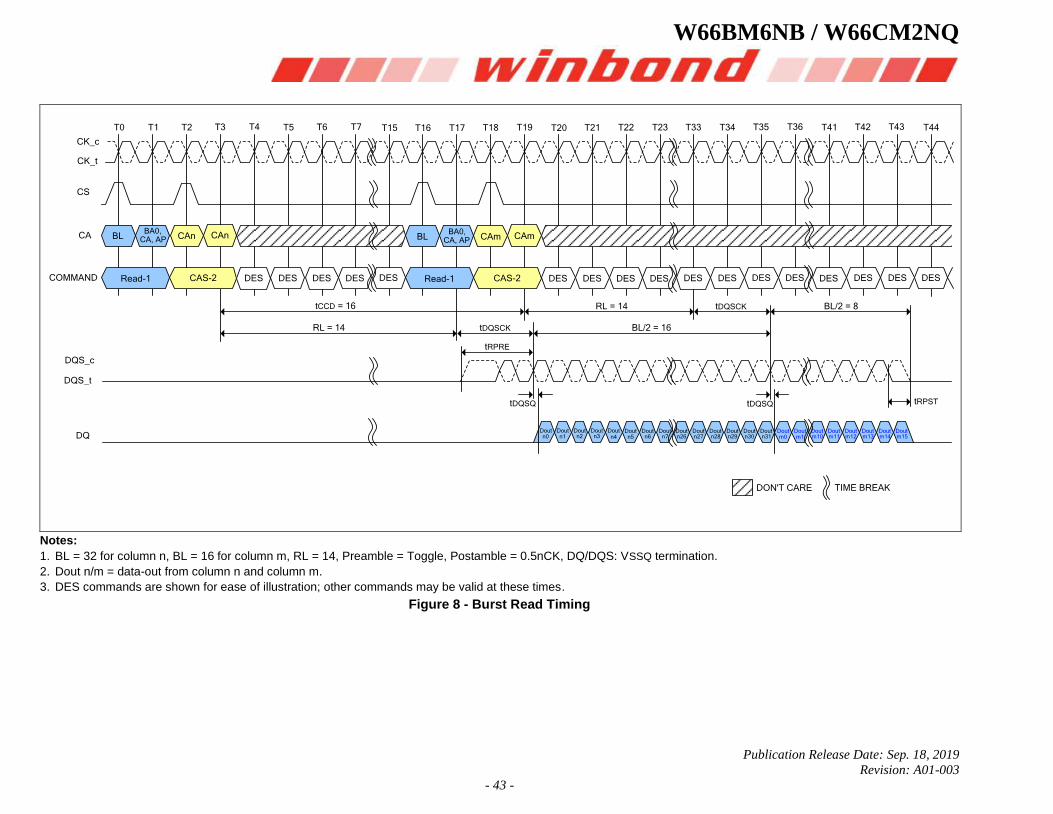
W66BM6NB / W66CM2NQ
Publication Release Date: Sep. 18, 2019
Revision: A01-003
- 43 -
Read-1 CAS-2 Read-1 CAS-2 DES DES DES DES DES DES DES DES DES DES DES DESDES DES DES DES DES
CAn CAnBLBA0,
CA, AP
tRPRE
tDQSQ
tDQSCK
tCCD = 16
RL = 14
RL = 14 tDQSCK
BL/2 = 16
BL/2 = 8
tDQSQ tRPST
T0 T1 T2 T3 T4 T5 T6 T7 T15 T16 T17 T18 T19 T20 T21 T22 T23 T33 T34 T35 T36 T41 T42 T43 T44
CK_c
CK_t
CS
CA
COMMAND
DQ
DQS_c
DQS_t
TIME BREAKDON'T CARE
Dout n0
Dout n1
Dout n2
Dout n3
Dout n4
Dout n5
Dout n6
Dout n7
Dout n26
Dout n27
Dout n28
Dout n29
Dout n30
Dout n31
Dout m0
Dout m1
Dout m10
Dout m11
Dout m12
Dout m13
Dout m14
Dout m15
CAm CAmBLBA0,
CA, AP
Notes:
1. BL = 32 for column n, BL = 16 for column m, RL = 14, Preamble = Toggle, Postamble = 0.5nCK, DQ/DQS: VSSQ termination.
2. Dout n/m = data-out from column n and column m.
3. DES commands are shown for ease of illustration; other commands may be valid at these times.
Figure 8 - Burst Read Timing
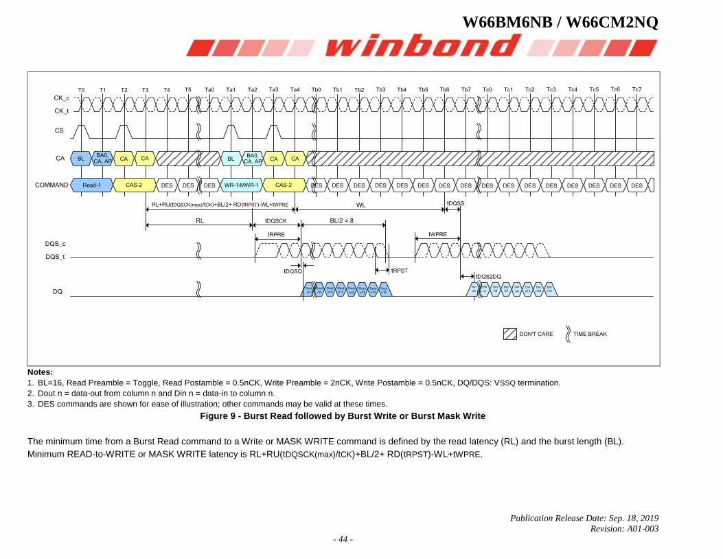
W66BM6NB / W66CM2NQ
Publication Release Date: Sep. 18, 2019
Revision: A01-003
- 44 -
tDQSQ
tDQSCK
tRPRE tWPRE
tDQSS
tRPSTtDQS2DQ
BL/2 = 8RL
WLRL+RU(tDQSCK(max)/tCK)+BL/2+ RD(tRPST)-WL+tWPRE
CA CABLBA0,
CA, AP
Read-1 CAS-2 WR-1/MWR-1 CAS-2DES DES DES DES DES DES DES DES DES DES DES DES DES DES DES DES DES DES DES
CA CABLBA0,
CA, AP
T0 T1 T2 T3 T4 T5 Ta0 Ta1 Ta2 Ta3 Ta4 Tb0 Tb1 Tb2 Tb3 Tb4 Tb5 Tb6 Tb7 Tc0 Tc1 Tc2 Tc3 Tc4 Tc5 Tc6 Tc7
CK_c
CK_t
CS
CA
COMMAND
DQS_c
DQS_t
DQ
TIME BREAKDON'T CARE
Dout
n0
Dout
n9
Dout
n10
Dout
n11
Dout
n12
Dout
n13
Dout
n14
Dout
n15
Din
n0
Din
n1
Din
n2
Din
n3
Din
n4
Din
n13
Din
n14
Din
n15
Notes:
1. BL=16, Read Preamble = Toggle, Read Postamble = 0.5nCK, Write Preamble = 2nCK, Write Postamble = 0.5nCK, DQ/DQS: VSSQ termination.
2. Dout n = data-out from column n and Din n = data-in to column n.
3. DES commands are shown for ease of illustration; other commands may be valid at these times.
Figure 9 - Burst Read followed by Burst Write or Burst Mask Write
The minimum time from a Burst Read command to a Write or MASK WRITE command is defined by the read latency (RL) and the burst length (BL).
Minimum READ-to-WRITE or MASK WRITE latency is RL+RU(tDQSCK(max)/tCK)+BL/2+ RD(tRPST)-WL+tWPRE.
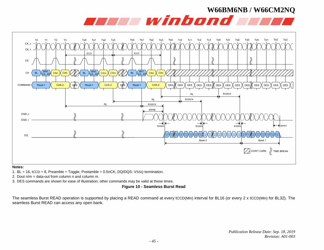
W66BM6NB / W66CM2NQ
Publication Release Date: Sep. 18, 2019
Revision: A01-003
- 45 -
tDQSQ
tDQSCK
tRPRE
tDQSQ tRPST
RL
RL
CAn CAnBLBA0,
CA, AP
Read-1 CAS-2 Read-1DES DES DES DES DES DES DES DES DES DES DES DES DES DES DES
CAm CAmBLBA0,
CA, AP
T0 T1 T2 T3 Ta0 Ta1 Ta2 Ta3 Tb0 Tb1 Tb2 Tb3 Tb4 Tc0 Tc1 Tc2 Tc3 Td0 Td1 Td2 Td3 Te0 Te1 Te2 Te3
CK_c
CK_t
CS
CA
COMMAND
DQS_c
DQS_t
DQ
TIME BREAKDON'T CARE
Dout
n0
Dout
n1
Dout
n10
Dout
n11
Dout
n12
Dout
n13
Dout
n14
Dout
n1
Dout
n10
Dout
n11
Dout
n12
Dout
n13
Dout
n14
Dout
n15
CAn CAnBLBA1,
CA, AP
CAS-2 Read-1 CAS-2
tDQSCK
tDQSCK
tDQSQ
RL
Dout
m1
Dout
m10
Dout
m11
Dout
m12
Dout
m13
Dout
m14
Dout
n15
Dout
m15
Dout
n0
Dout
m0
Bank 0 Bank 1
tCCDtCCD
Notes:
1. BL = 16, tCCD = 8, Preamble = Toggle, Postamble = 0.5nCK, DQ/DQS: VSSQ termination.
2. Dout n/m = data-out from column n and column m.
3. DES commands are shown for ease of illustration; other commands may be valid at these times.
Figure 10 - Seamless Burst Read
The seamless Burst READ operation is supported by placing a READ command at every tCCD(Min) interval for BL16 (or every 2 x tCCD(Min) for BL32). The seamless Burst READ can access any open bank.
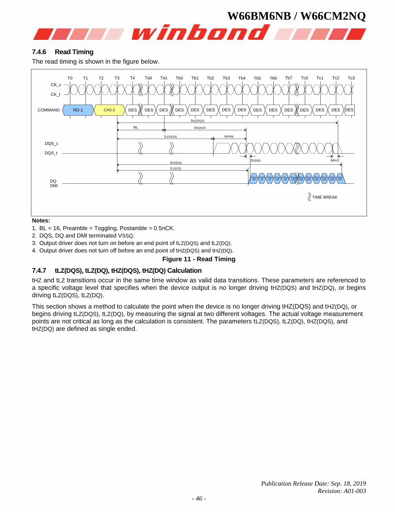
W66BM6NB / W66CM2NQ
Publication Release Date: Sep. 18, 2019
Revision: A01-003
- 46 -
7.4.6 Read Timing
The read timing is shown in the figure below.
TIME BREAK
CK_c
CK_t
COMMAND
DQS_c
DQS_t
DQ
T0 T1 T2 T3 T4 Ta0 Ta1 Tb0 Tb1 Tb2 Tb3 Tb4 Tb5 Tb6 Tb7 Tc0 Tc1 Tc2 Tc3
RL tDQSCK
tRPRE
tRPSTtDQSQ
DES DES DES DES DES DES DES DES DES DES DES DES DES DES DES
Dout n0
Dout n1
Dout n2
Dout n3
Dout n4
Dout n5
Dout n10
Dout n11
Dout n12
Dout n13
Dout n14
Dout n15
tHZ(DQS)
tLZ(DQS)
tHZ(DQ)
tLZ(DQ)
DMI
RD-1 CAS-2
Notes:
1. BL = 16, Preamble = Toggling, Postamble = 0.5nCK.
2. DQS, DQ and DMI terminated VSSQ.
3. Output driver does not turn on before an end point of tLZ(DQS) and tLZ(DQ).
4. Output driver does not turn off before an end point of tHZ(DQS) and tHZ(DQ).
Figure 11 - Read Timing
7.4.7 tLZ(DQS), tLZ(DQ), tHZ(DQS), tHZ(DQ) Calculation
tHZ and tLZ transitions occur in the same time window as valid data transitions. These parameters are referenced to a specific voltage level that specifies when the device output is no longer driving tHZ(DQS) and tHZ(DQ), or begins driving tLZ(DQS), tLZ(DQ).
This section shows a method to calculate the point when the device is no longer driving tHZ(DQS) and tHZ(DQ), or begins driving tLZ(DQS), tLZ(DQ), by measuring the signal at two different voltages. The actual voltage measurement points are not critical as long as the calculation is consistent. The parameters tLZ(DQS), tLZ(DQ), tHZ(DQS), and tHZ(DQ) are defined as single ended.
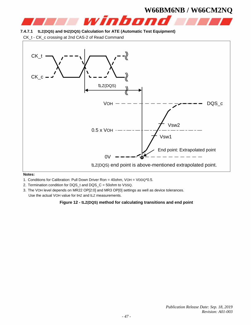
W66BM6NB / W66CM2NQ
Publication Release Date: Sep. 18, 2019
Revision: A01-003
- 47 -
7.4.7.1 tLZ(DQS) and tHZ(DQS) Calculation for ATE (Automatic Test Equipment)
CK_t - CK_c crossing at 2nd CAS-2 of Read Command
CK_t
CK_c
tLZ(DQS)
tLZ(DQS) end point is above-mentioned extrapolated point.
End point: Extrapolated point
Vsw2
Vsw1
DQS_cVOH
0V
0.5 x VOH
Notes:
1. Conditions for Calibration: Pull Down Driver Ron = 40ohm, VOH = VDDQ*0.5.
2. Termination condition for DQS_t and DQS_C = 50ohm to VSSQ.
3. The VOH level depends on MR22 OP[2:0] and MR3 OP[0] settings as well as device tolerances.
Use the actual VOH value for tHZ and tLZ measurements.
Figure 12 - tLZ(DQS) method for calculating transitions and end point
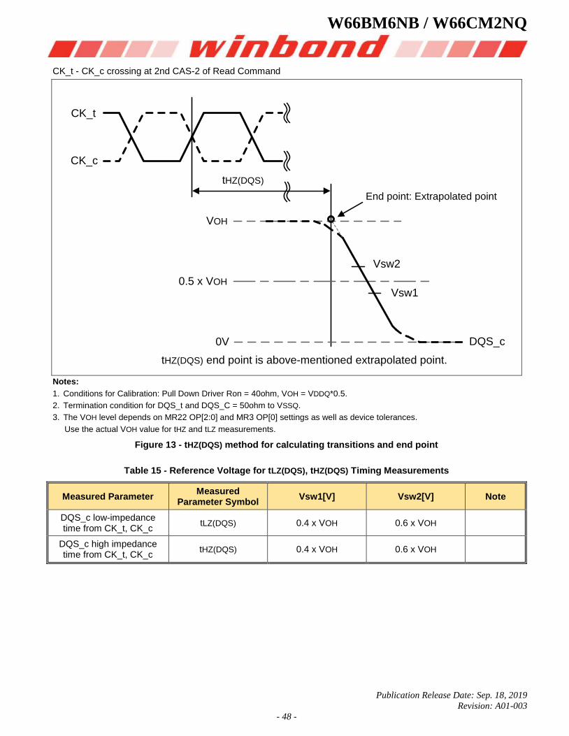
W66BM6NB / W66CM2NQ
Publication Release Date: Sep. 18, 2019
Revision: A01-003
- 48 -
CK_t - CK_c crossing at 2nd CAS-2 of Read Command
CK_t
CK_c
tHZ(DQS)
tHZ(DQS) end point is above-mentioned extrapolated point.
Vsw2
Vsw1
DQS_c
VOH
0V
0.5 x VOH
End point: Extrapolated point
Notes:
1. Conditions for Calibration: Pull Down Driver Ron = 40ohm, VOH = VDDQ*0.5.
2. Termination condition for DQS_t and DQS_C = 50ohm to VSSQ.
3. The VOH level depends on MR22 OP[2:0] and MR3 OP[0] settings as well as device tolerances.
Use the actual VOH value for tHZ and tLZ measurements.
Figure 13 - tHZ(DQS) method for calculating transitions and end point
Table 15 - Reference Voltage for tLZ(DQS), tHZ(DQS) Timing Measurements
Measured Parameter Measured
Parameter Symbol Vsw1[V] Vsw2[V] Note
DQS_c low-impedance time from CK_t, CK_c
tLZ(DQS) 0.4 x VOH 0.6 x VOH
DQS_c high impedance time from CK_t, CK_c
tHZ(DQS) 0.4 x VOH 0.6 x VOH
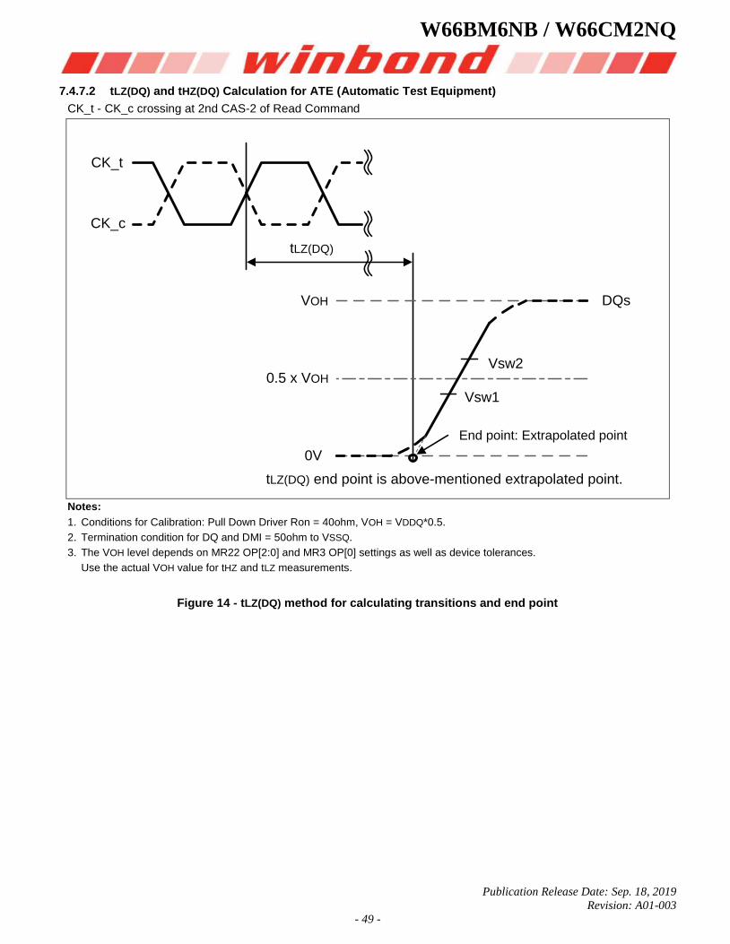
W66BM6NB / W66CM2NQ
Publication Release Date: Sep. 18, 2019
Revision: A01-003
- 49 -
7.4.7.2 tLZ(DQ) and tHZ(DQ) Calculation for ATE (Automatic Test Equipment)
CK_t - CK_c crossing at 2nd CAS-2 of Read Command
CK_t
CK_c
tLZ(DQ)
tLZ(DQ) end point is above-mentioned extrapolated point.
End point: Extrapolated point
Vsw2
Vsw1
DQsVOH
0V
0.5 x VOH
Notes:
1. Conditions for Calibration: Pull Down Driver Ron = 40ohm, VOH = VDDQ*0.5.
2. Termination condition for DQ and DMI = 50ohm to VSSQ.
3. The VOH level depends on MR22 OP[2:0] and MR3 OP[0] settings as well as device tolerances.
Use the actual VOH value for tHZ and tLZ measurements.
Figure 14 - tLZ(DQ) method for calculating transitions and end point
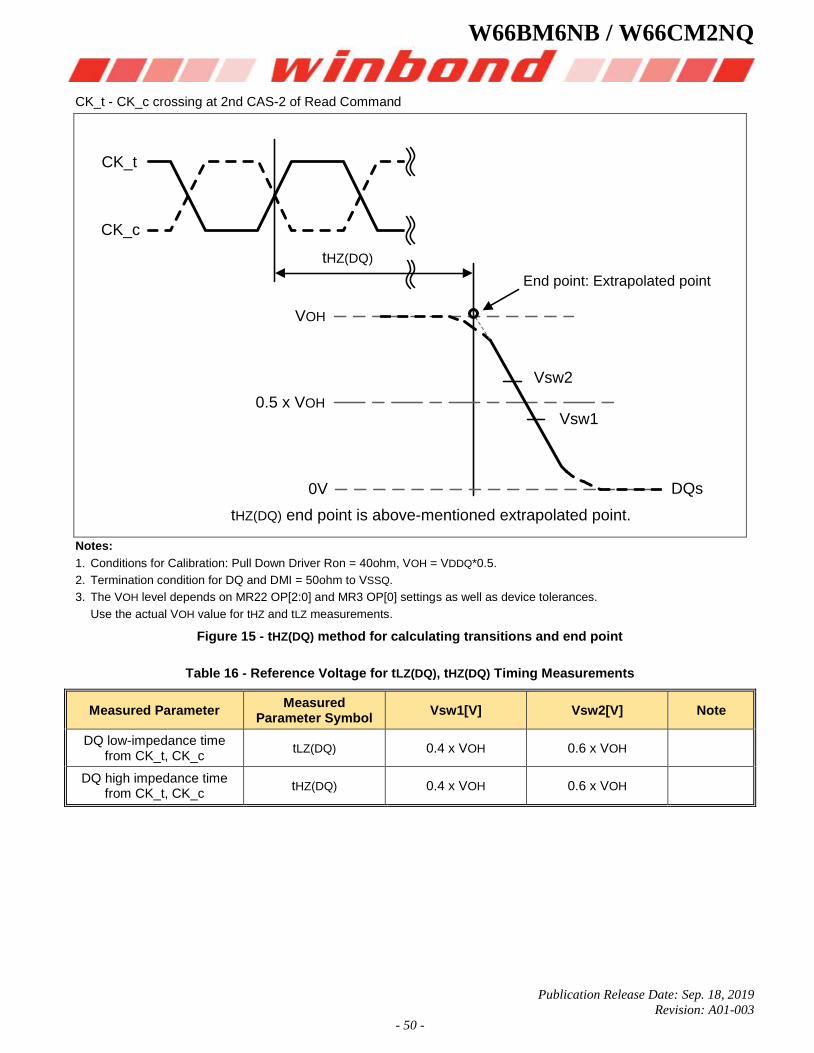
W66BM6NB / W66CM2NQ
Publication Release Date: Sep. 18, 2019
Revision: A01-003
- 50 -
CK_t - CK_c crossing at 2nd CAS-2 of Read Command
CK_t
CK_c
tHZ(DQ)
tHZ(DQ) end point is above-mentioned extrapolated point.
Vsw2
Vsw1
DQs
VOH
0V
0.5 x VOH
End point: Extrapolated point
Notes:
1. Conditions for Calibration: Pull Down Driver Ron = 40ohm, VOH = VDDQ*0.5.
2. Termination condition for DQ and DMI = 50ohm to VSSQ.
3. The VOH level depends on MR22 OP[2:0] and MR3 OP[0] settings as well as device tolerances.
Use the actual VOH value for tHZ and tLZ measurements.
Figure 15 - tHZ(DQ) method for calculating transitions and end point
Table 16 - Reference Voltage for tLZ(DQ), tHZ(DQ) Timing Measurements
Measured Parameter Measured
Parameter Symbol Vsw1[V] Vsw2[V] Note
DQ low-impedance time from CK_t, CK_c
tLZ(DQ) 0.4 x VOH 0.6 x VOH
DQ high impedance time from CK_t, CK_c
tHZ(DQ) 0.4 x VOH 0.6 x VOH
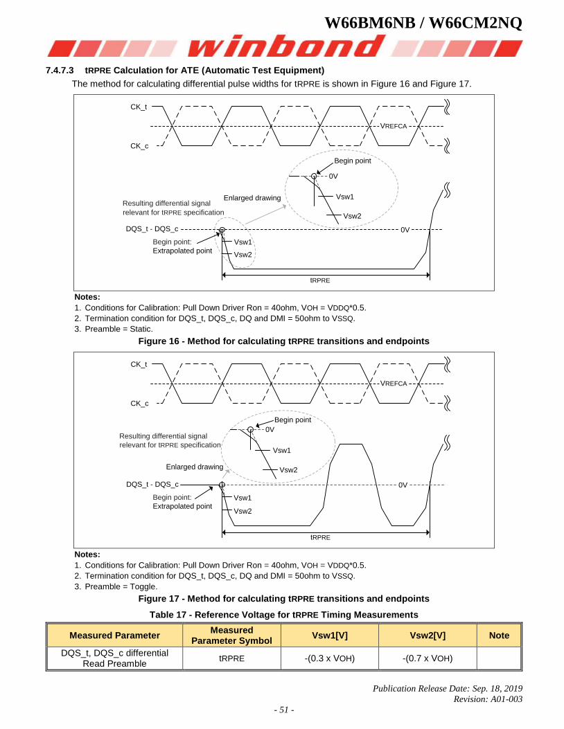
W66BM6NB / W66CM2NQ
Publication Release Date: Sep. 18, 2019
Revision: A01-003
- 51 -
7.4.7.3 tRPRE Calculation for ATE (Automatic Test Equipment)
The method for calculating differential pulse widths for tRPRE is shown in Figure 16 and Figure 17.
Enlarged drawing
relevant for tRPRE specification
Begin point:
Extrapolated point
DQS_t - DQS_c
tRPRE
0V
Vsw1
Vsw2
0V
CK_t
CK_c
Begin point
Vsw1
Vsw2
VREFCA
Resulting differential signal
Notes:
1. Conditions for Calibration: Pull Down Driver Ron = 40ohm, VOH = VDDQ*0.5.
2. Termination condition for DQS_t, DQS_c, DQ and DMI = 50ohm to VSSQ.
3. Preamble = Static.
Figure 16 - Method for calculating tRPRE transitions and endpoints
CK_t
CK_c
VREFCA
Vsw1
Vsw2
tRPRE
0V
0V
Vsw1
Vsw2
Begin point
relevant for tRPRE specification
Begin point:
Extrapolated point
DQS_t - DQS_c
Resulting differential signal
Enlarged drawing
Notes:
1. Conditions for Calibration: Pull Down Driver Ron = 40ohm, VOH = VDDQ*0.5.
2. Termination condition for DQS_t, DQS_c, DQ and DMI = 50ohm to VSSQ.
3. Preamble = Toggle.
Figure 17 - Method for calculating tRPRE transitions and endpoints
Table 17 - Reference Voltage for tRPRE Timing Measurements
Measured Parameter Measured
Parameter Symbol Vsw1[V] Vsw2[V] Note
DQS_t, DQS_c differential Read Preamble
tRPRE -(0.3 x VOH) -(0.7 x VOH)
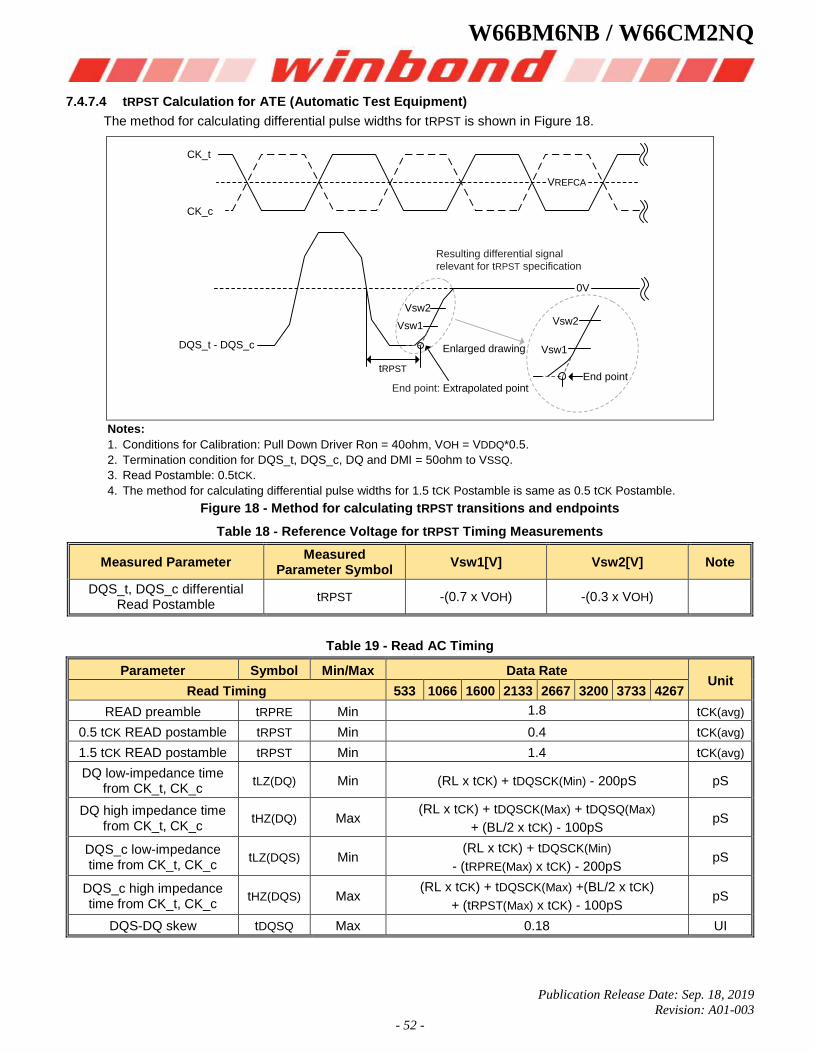
W66BM6NB / W66CM2NQ
Publication Release Date: Sep. 18, 2019
Revision: A01-003
- 52 -
7.4.7.4 tRPST Calculation for ATE (Automatic Test Equipment)
The method for calculating differential pulse widths for tRPST is shown in Figure 18.
CK_t
CK_c
VREFCA
Vsw1
Vsw2
End point
Enlarged drawing
End point: Extrapolated point
Vsw1
Vsw2
tRPST
DQS_t - DQS_c
0V
relevant for tRPST specificationResulting differential signal
Notes:
1. Conditions for Calibration: Pull Down Driver Ron = 40ohm, VOH = VDDQ*0.5.
2. Termination condition for DQS_t, DQS_c, DQ and DMI = 50ohm to VSSQ.
3. Read Postamble: 0.5tCK.
4. The method for calculating differential pulse widths for 1.5 tCK Postamble is same as 0.5 tCK Postamble.
Figure 18 - Method for calculating tRPST transitions and endpoints
Table 18 - Reference Voltage for tRPST Timing Measurements
Measured Parameter Measured
Parameter Symbol Vsw1[V] Vsw2[V] Note
DQS_t, DQS_c differential Read Postamble
tRPST -(0.7 x VOH) -(0.3 x VOH)
Table 19 - Read AC Timing
Parameter Symbol Min/Max Data Rate Unit
Read Timing 533 1066 1600 2133 2667 3200 3733 4267
READ preamble tRPRE Min 1.8 tCK(avg)
0.5 tCK READ postamble tRPST Min 0.4 tCK(avg)
1.5 tCK READ postamble tRPST Min 1.4 tCK(avg)
DQ low-impedance time from CK_t, CK_c
tLZ(DQ) Min (RL x tCK) + tDQSCK(Min) - 200pS pS
DQ high impedance time from CK_t, CK_c
tHZ(DQ) Max (RL x tCK) + tDQSCK(Max) + tDQSQ(Max)
+ (BL/2 x tCK) - 100pS pS
DQS_c low-impedance time from CK_t, CK_c
tLZ(DQS) Min (RL x tCK) + tDQSCK(Min)
- (tRPRE(Max) x tCK) - 200pS pS
DQS_c high impedance time from CK_t, CK_c
tHZ(DQS) Max (RL x tCK) + tDQSCK(Max) +(BL/2 x tCK)
+ (tRPST(Max) x tCK) - 100pS pS
DQS-DQ skew tDQSQ Max 0.18 UI
W66BM6NB / W66CM2NQ
Publication Release Date: Sep. 18, 2019
Revision: A01-003
- 53 -
7.4.8 tDQSCK Timing Table
Table 20 - tDQSCK Timing Table
Parameter Symbol Min Max Unit Notes
DQS Output Access Time from CK_t/CK_c tDQSCK 1.5 3.5 nS 1
DQS Output Access Time from CK_t/CK_c -
Temperature Variation tDQSCK_temp - 4 pS/°C 2
DQS Output Access Time from CK_t/CK_c -
Voltage Variation tDQSCK_volt - 7 pS/mV 3
Notes:
1. Includes DRAM process, voltage and temperature variation. It includes the AC noise impact for frequencies > 20 MHz and max voltage of 45 mV pk-pk from DC-20 MHz at a fixed temperature on the package. The voltage supply noise must comply with the component Min-Max DC Operating conditions.
2. tDQSCK_temp max delay variation as a function of Temperature.
3. tDQSCK_volt max delay variation as a function of DC voltage variation for VDDQ and VDD2. tDQSCK_volt should be used to calculate timing variation due to VDDQ and VDD2 noise < 20 MHz. Host controller do not need to account for any variation due to VDDQ and VDD2 noise > 20 MHz. The voltage supply noise must comply with the component Min-Max DC Operating conditions.
The voltage variation is defined as the
Max[abs{tDQSCKmin@V1- tDQSCKmax@V2}, abs{tDQSCKmax@V1-tDQSCKmin@V2}]/abs{V1-V2}.
For tester measurement VDDQ = VDD2 is assumed.
7.4.8.1 CK to DQS Rank to Rank variation
Table 21 - tDQSCK_rank2rank Timing Table
Parameter Symbol Min/Max Data Rate Unit Notes
Read Timing 1600 1866 2133 2400 3200 3733 4267
CK to DQS Rank to Rank variation
tDQSCK_rank2rank Max 1.0 nS 1, 2
Notes:
1. The same voltage and temperature are applied to tDQS2CK_rank2rank.
2. tDQSCK_rank2rank parameter is applied to multi-ranks per byte lane within a package consisting of the same design dies.
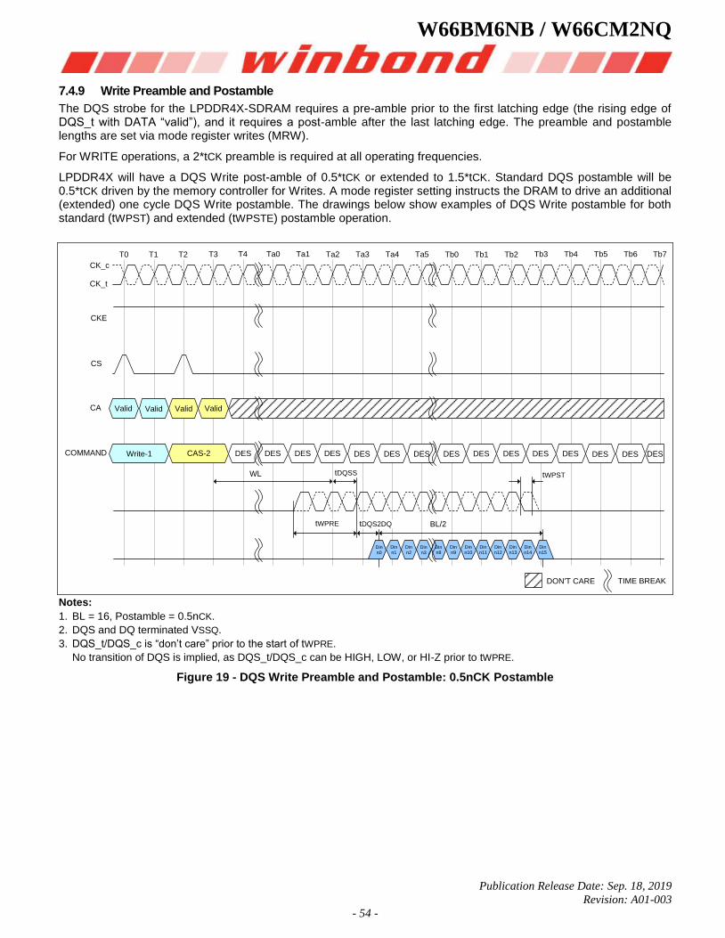
W66BM6NB / W66CM2NQ
Publication Release Date: Sep. 18, 2019
Revision: A01-003
- 54 -
7.4.9 Write Preamble and Postamble
The DQS strobe for the LPDDR4X-SDRAM requires a pre-amble prior to the first latching edge (the rising edge of DQS_t with DATA “valid”), and it requires a post-amble after the last latching edge. The preamble and postamble lengths are set via mode register writes (MRW).
For WRITE operations, a 2*tCK preamble is required at all operating frequencies.
LPDDR4X will have a DQS Write post-amble of 0.5*tCK or extended to 1.5*tCK. Standard DQS postamble will be 0.5*tCK driven by the memory controller for Writes. A mode register setting instructs the DRAM to drive an additional (extended) one cycle DQS Write postamble. The drawings below show examples of DQS Write postamble for both standard (tWPST) and extended (tWPSTE) postamble operation.
CK_c
CK_t
T0 T1 T2 T3 T4 Ta0 Ta1 Ta2 Ta3 Ta4 Ta5 Tb0 Tb1 Tb2 Tb3 Tb4 Tb5 Tb6 Tb7
Write-1 CAS-2
Valid Valid ValidValid
Din n0
Din n1
Din n2
Din n3
Din n8
Din n9
Din n10
Din n11
Din n12
Din n13
Din n14
Din n15
tWPSTtDQSS
tWPRE tDQS2DQ BL/2
WL
DES DESDES DES DES DES DES DES DES DES DES DES DES DES DESCOMMAND
CKE
CS
CA
DON'T CARE TIME BREAK
Notes:
1. BL = 16, Postamble = 0.5nCK.
2. DQS and DQ terminated VSSQ.
3. DQS_t/DQS_c is “don’t care” prior to the start of tWPRE.
No transition of DQS is implied, as DQS_t/DQS_c can be HIGH, LOW, or HI-Z prior to tWPRE.
Figure 19 - DQS Write Preamble and Postamble: 0.5nCK Postamble
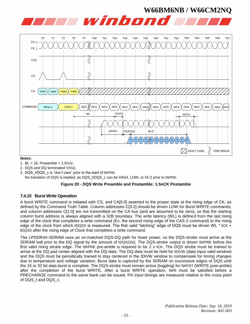
W66BM6NB / W66CM2NQ
Publication Release Date: Sep. 18, 2019
Revision: A01-003
- 55 -
CK_c
CK_t
T0 T1 T2 T3 T4 Ta0 Ta1 Ta2 Ta3 Ta4 Ta5 Tb0 Tb1 Tb2 Tb3 Tb4 Tb5 Tb6 Tb7
Write-1 CAS-2
Valid Valid ValidValid
Din n0
Din n1
Din n2
Din n3
Din n8
Din n9
Din n10
Din n11
Din n12
Din n13
Din n14
Din n15
tWPSTtDQSS
tWPRE tDQS2DQ BL/2
WL
DES DESDES DES DES DES DES DES DES DES DES DES DES DES DESCOMMAND
CKE
CS
CA
DON'T CARE TIME BREAK
Notes:
1. BL = 16, Postamble = 1.5nCK.
2. DQS and DQ terminated VSSQ.
3. DQS_t/DQS_c is “don’t care” prior to the start of tWPRE.
No transition of DQS is implied, as DQS_t/DQS_c can be HIGH, LOW, or HI-Z prior to tWPRE.
Figure 20 - DQS Write Preamble and Postamble: 1.5nCK Postamble
7.4.10 Burst Write Operation
A burst WRITE command is initiated with CS, and CA[5:0] asserted to the proper state at the rising edge of CK, as defined by the Command Truth Table. Column addresses C[3:2] should be driven LOW for Burst WRITE commands, and column addresses C[1:0] are not transmitted on the CA bus (and are assumed to be zero), so that the starting column burst address is always aligned with a 32B boundary. The write latency (WL) is defined from the last rising edge of the clock that completes a write command (Ex: the second rising edge of the CAS-2 command) to the rising edge of the clock from which tDQSS is measured. The first valid “latching” edge of DQS must be driven WL * tCK + tDQSS after the rising edge of Clock that completes a write command.
The LPDDR4X-SDRAM uses an un-matched DQS-DQ path for lower power, so the DQS-strobe must arrive at the SDRAM ball prior to the DQ signal by the amount of tDQS2DQ. The DQS-strobe output is driven tWPRE before the first valid rising strobe edge. The tWPRE pre-amble is required to be 2 x tCK. The DQS strobe must be trained to arrive at the DQ pad center-aligned with the DQ-data. The DQ-data must be held for tDIVW (data input valid window) and the DQS must be periodically trained to stay centered in the tDIVW window to compensate for timing changes due to temperature and voltage variation. Burst data is captured by the SDRAM on successive edges of DQS until the 16 or 32 bit data burst is complete. The DQS-strobe must remain active (toggling) for tWPST (WRITE post-amble) after the completion of the burst WRITE. After a burst WRITE operation, tWR must be satisfied before a PRECHARGE command to the same bank can be issued. Pin input timings are measured relative to the cross point of DQS_t and DQS_c.
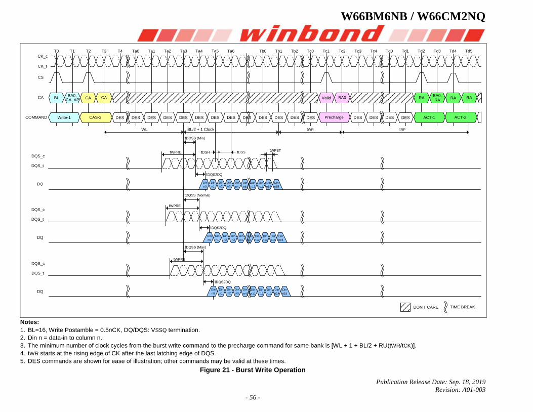
W66BM6NB / W66CM2NQ
Publication Release Date: Sep. 18, 2019
Revision: A01-003
- 56 -
T0 T1 T2 T3 Ta0 Ta1 Ta2 Ta3 Ta5 Ta6T4 Tb0 Tb1 Tb2 Tc0 Tc1 Tc2 Tc3 Tc4 Td0 Td1 Td2 Td3 Td4 Td5
CK_c
CK_t
Ta4
CA CABLBA0,
CA, AP Valid BA0 RA RARABA0,RA
Write-1 CAS-2 DES DES DES DES DES DES DES DES DES DES DES DES DES Precharge DES DES DES DES ACT-1 ACT-2
Din
n0
Din
n1
Din
n2
Din
n3
Din
n4
Din
n5
Din
n12
Din
n13
Din
n14
Din
n15
Din
n0
Din
n1
Din
n2
Din
n3
Din
n4
Din
n11
Din
n12
Din
n13
Din
n14
Din
n15
Din
n0
Din
n1
Din
n2
Din
n3
Din
n4
Din
n11
Din
n12
Din
n13
Din
n14
Din
n15
tWPRE
CS
CA
COMMAND
DQS_c
DQS_t
DQ
DQS_c
DQS_t
DQ
DQS_c
DQS_t
DQ
WL
tWPSTtDSS
tDQSS (Min)
tDQSS (Normal)
tDQSS (Max)
tWPRE
tWPRE
tDQS2DQ
tDQS2DQ
tDQS2DQ
tDSH
tWR tRPBL/2 + 1 Clock
TIME BREAKDON'T CARE
Notes:
1. BL=16, Write Postamble = 0.5nCK, DQ/DQS: VSSQ termination.
2. Din n = data-in to column n.
3. The minimum number of clock cycles from the burst write command to the precharge command for same bank is [WL + 1 + BL/2 + RU(tWR/tCK)].
4. tWR starts at the rising edge of CK after the last latching edge of DQS.
5. DES commands are shown for ease of illustration; other commands may be valid at these times.
Figure 21 - Burst Write Operation
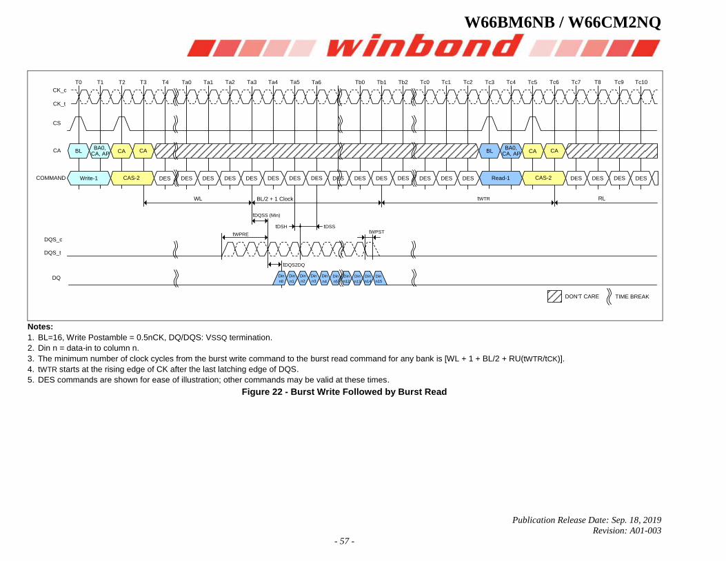
W66BM6NB / W66CM2NQ
Publication Release Date: Sep. 18, 2019
Revision: A01-003
- 57 -
T0 T1 T2 T3 Ta0 Ta1 Ta2 Ta3 Ta5 Ta6T4 Tb0 Tb1 Tb2 Tc0 Tc1 Tc2 Tc3 Tc4 Tc5 Tc6 Tc7 T8 Tc9 Tc10
CK_c
CK_t
Ta4
CA CABLBA0,
CA, AP
CS
CA CA CABLBA0,
CA, AP
Write-1 CAS-2 DES DES DES DES DES DES DES DES DES DES DES DES DESCOMMAND DES DES Read-1 CAS-2 DES DES DES DES
tWPREDQS_c
DQS_t
tWPSTtDSH tDSS
Din
n0
Din
n1
Din
n2
Din
n3
Din
n4
Din
n5
Din
n12
Din
n13
Din
n14
Din
n15DQ
tDQS2DQ
tDQSS (Min)
WL BL/2 + 1 Clock tWTR RL
TIME BREAKDON'T CARE
Notes:
1. BL=16, Write Postamble = 0.5nCK, DQ/DQS: VSSQ termination.
2. Din n = data-in to column n.
3. The minimum number of clock cycles from the burst write command to the burst read command for any bank is [WL + 1 + BL/2 + RU(tWTR/tCK)].
4. tWTR starts at the rising edge of CK after the last latching edge of DQS.
5. DES commands are shown for ease of illustration; other commands may be valid at these times.
Figure 22 - Burst Write Followed by Burst Read
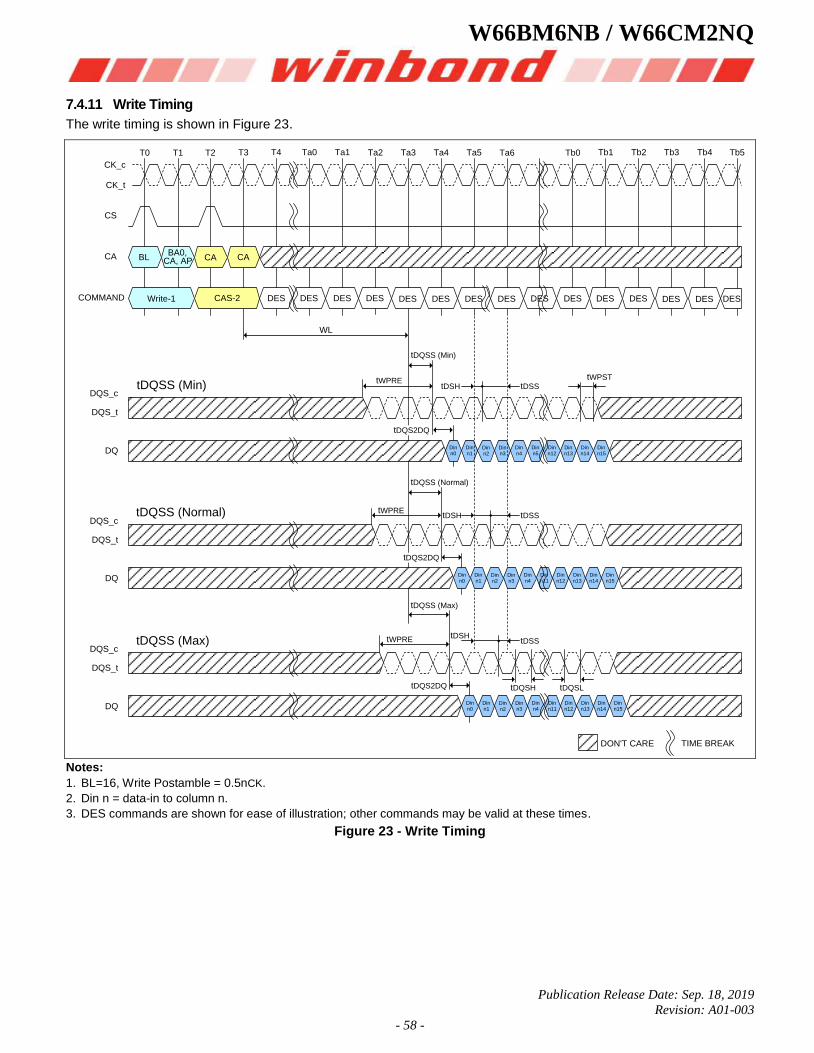
W66BM6NB / W66CM2NQ
Publication Release Date: Sep. 18, 2019
Revision: A01-003
- 58 -
7.4.11 Write Timing
The write timing is shown in Figure 23.
CK_c
CK_t
T0 T1 T2 T3 T4 Ta0 Ta1 Ta2 Ta3 Ta4 Ta5 Ta6 Tb0 Tb1 Tb2 Tb3 Tb4 Tb5
CS
BL CA, AP CACACA BA0,
Write-1 CAS-2 DES DESDES DES DES DES DES DES DES DES DES DES DES DES DESCOMMAND
Din n0
Din n1
Din n2
Din n3
Din n4
Din n5
Din n12
Din n13
Din n14
Din n15
Din n0
Din n1
Din n2
Din n3
Din n4
Din n11
Din n12
Din n13
Din n14
Din n15
tWPRE
tWPRE
tDQSS (Min)
tDQSS (Max)
tDQS2DQ
tDQS2DQ
tDSStDSHtWPST
WL
DQS_c
DQS_t
DQ
DQS_c
DQS_t
DQ
DON'T CARE TIME BREAK
Din n0
Din n1
Din n2
Din n3
Din n4
Din n11
Din n12
Din n13
Din n14
Din n15
tWPRE
tDQSS (Normal)
DQS_c
DQS_t
DQ
tDQSS (Min)
tDQSS (Max)
tDQSS (Normal) tDSStDSH
tDQS2DQ
tDQSH tDQSL
tDSStDSH
Notes:
1. BL=16, Write Postamble = 0.5nCK.
2. Din n = data-in to column n.
3. DES commands are shown for ease of illustration; other commands may be valid at these times.
Figure 23 - Write Timing
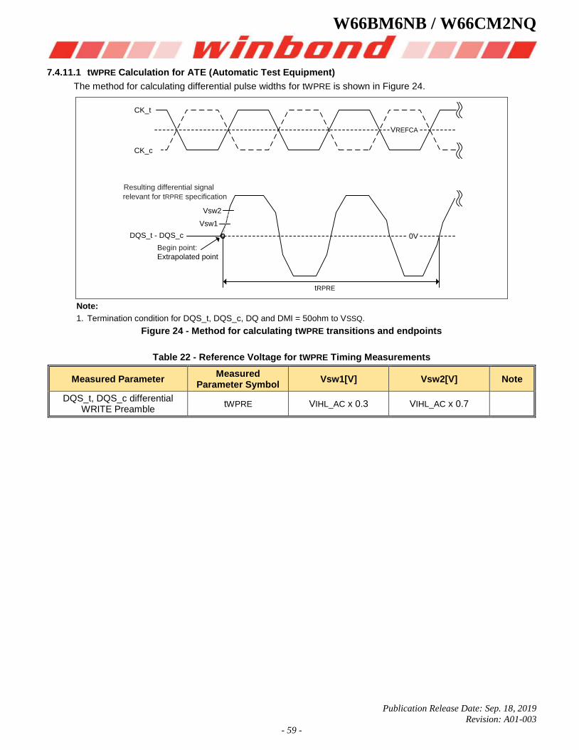
W66BM6NB / W66CM2NQ
Publication Release Date: Sep. 18, 2019
Revision: A01-003
- 59 -
7.4.11.1 tWPRE Calculation for ATE (Automatic Test Equipment)
The method for calculating differential pulse widths for tWPRE is shown in Figure 24.
CK_t
CK_c
VREFCA
tRPRE
0V
Vsw1
Vsw2
relevant for tRPRE specification
Resulting differential signal
DQS_t - DQS_c
Begin point:
Extrapolated point
Note:
1. Termination condition for DQS_t, DQS_c, DQ and DMI = 50ohm to VSSQ.
Figure 24 - Method for calculating tWPRE transitions and endpoints
Table 22 - Reference Voltage for tWPRE Timing Measurements
Measured Parameter Measured
Parameter Symbol Vsw1[V] Vsw2[V] Note
DQS_t, DQS_c differential WRITE Preamble
tWPRE VIHL_AC x 0.3 VIHL_AC x 0.7
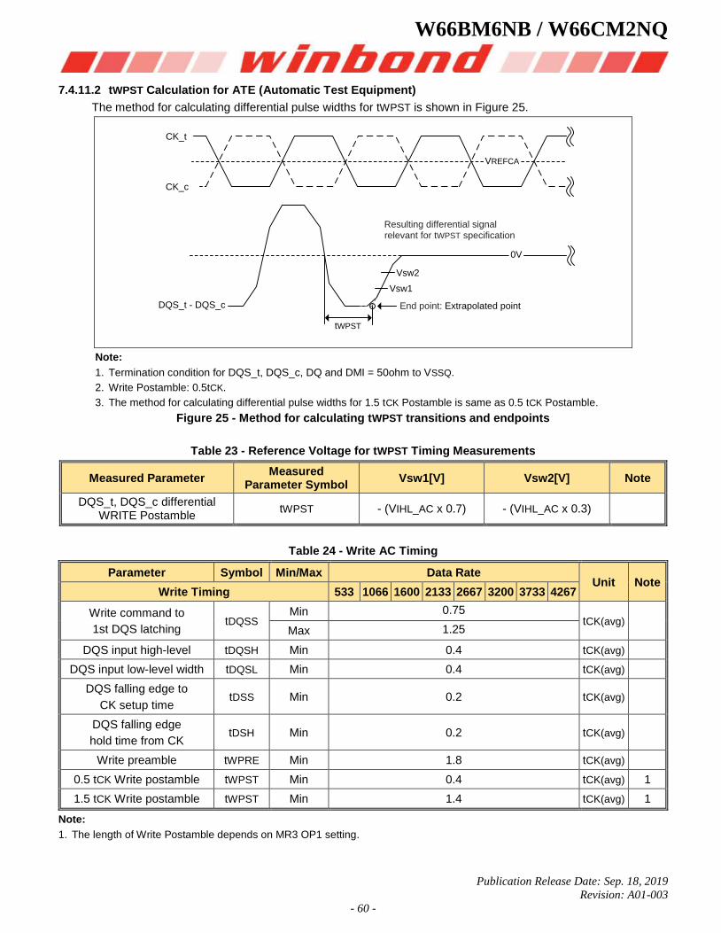
W66BM6NB / W66CM2NQ
Publication Release Date: Sep. 18, 2019
Revision: A01-003
- 60 -
7.4.11.2 tWPST Calculation for ATE (Automatic Test Equipment)
The method for calculating differential pulse widths for tWPST is shown in Figure 25.
CK_t
CK_c
VREFCA
End point: Extrapolated point
Vsw1
Vsw2
tWPST
DQS_t - DQS_c
0V
relevant for tWPST specificationResulting differential signal
Note:
1. Termination condition for DQS_t, DQS_c, DQ and DMI = 50ohm to VSSQ.
2. Write Postamble: 0.5tCK.
3. The method for calculating differential pulse widths for 1.5 tCK Postamble is same as 0.5 tCK Postamble.
Figure 25 - Method for calculating tWPST transitions and endpoints
Table 23 - Reference Voltage for tWPST Timing Measurements
Measured Parameter Measured
Parameter Symbol Vsw1[V] Vsw2[V] Note
DQS_t, DQS_c differential WRITE Postamble
tWPST - (VIHL_AC x 0.7) - (VIHL_AC x 0.3)
Table 24 - Write AC Timing
Parameter Symbol Min/Max Data Rate Unit Note
Write Timing 533 1066 1600 2133 2667 3200 3733 4267
Write command to
1st DQS latching tDQSS
Min 0.75 tCK(avg)
Max 1.25
DQS input high-level tDQSH Min 0.4 tCK(avg)
DQS input low-level width tDQSL Min 0.4 tCK(avg)
DQS falling edge to
CK setup time tDSS Min 0.2 tCK(avg)
DQS falling edge
hold time from CK tDSH Min 0.2 tCK(avg)
Write preamble tWPRE Min 1.8 tCK(avg)
0.5 tCK Write postamble tWPST Min 0.4 tCK(avg) 1
1.5 tCK Write postamble tWPST Min 1.4 tCK(avg) 1
Note:
1. The length of Write Postamble depends on MR3 OP1 setting.
W66BM6NB / W66CM2NQ
Publication Release Date: Sep. 18, 2019
Revision: A01-003
- 61 -
7.4.12 Read and Write Latencies
Table 25 - Read and Write Latencies
Read Latency Write Latency
nWR nRTP
Lower Clock Frequency Limit [MHz]
(>)
Upper Clock Frequency Limit [MHz]
(≤)
Notes No DBI w/ DBI Set A Set B
6 6 4 4 6 8 10 266
1, 2, 3, 4, 5, 6
10 12 6 8 10 8 266 533
14 16 8 12 16 8 533 800
20 22 10 18 20 8 800 1066
24 28 12 22 24 10 1066 1333
28 32 14 26 30 12 1333 1600
32 36 16 30 34 14 1600 1866
36 40 18 34 40 16 1866 2133
Notes:
1. The LPDDR4X SDRAM device should not be operated at a frequency above the Upper Frequency Limit, or below the Lower Frequency Limit, shown for each RL, WL, nRTP, or nWR value.
2. DBI for Read operations is enabled in MR3 OP[6]. When MR3 OP[6]=0, then the “No DBI” column should be used for Read Latency. When MR3 OP[6]=1, then the “w/DBI” column should be used for Read Latency.
3. Write Latency Set “A” and Set “B” is determined by MR2 OP[6]. When MR2 OP[6]=0, then Write Latency Set “A” should be used. When MR2 OP[6]=1, then Write Latency Set “B” should be used.
4. The programmed value of nWR is the number of clock cycles the LPDDR4X SDRAM device uses to determine the starting point of an internal Precharge operation after a Write burst with AP (Auto Precharge). It is determined by RU(tWR/tCK).
5. The programmed value of nRTP is the number of clock cycles the LPDDR4X SDRAM device uses to determine the starting point of an internal Precharge operation after a Read burst with AP (Auto Precharge). It is determined by RU(tRTP/tCK).
6. nRTP shown in this table is valid for BL16 only. For BL32, the SDRAM will add 8 clocks to the nRTP value before starting a precharge.
7.4.13 Write and Masked Write operation DQS controls (WDQS Control)
LPDDR4X-SDRAMs support write and masked write operations with the following DQS controls. Before and after Write and Masked Write operations are issued, DQS_t/DQS_c is required to have a sufficient voltage gap to make sure the write buffers operating normally without any risk of metastability.
The LPDDR4X-SDRAM is supported by either of two WDQS control modes below.
Mode 1: Read Based Control
Mode 2: WDQS_on / WDQS_off definition based control
Regardless of ODT enable/disable, WDQS related timing described here does not allow any change of existing command timing constraints for all read/write operation. In case of any conflict or ambiguity on the command timing constraints caused by the spec here, the spec defined in section 7.4.35, table 70 (or below) should have higher priority than WDQS control requirements.
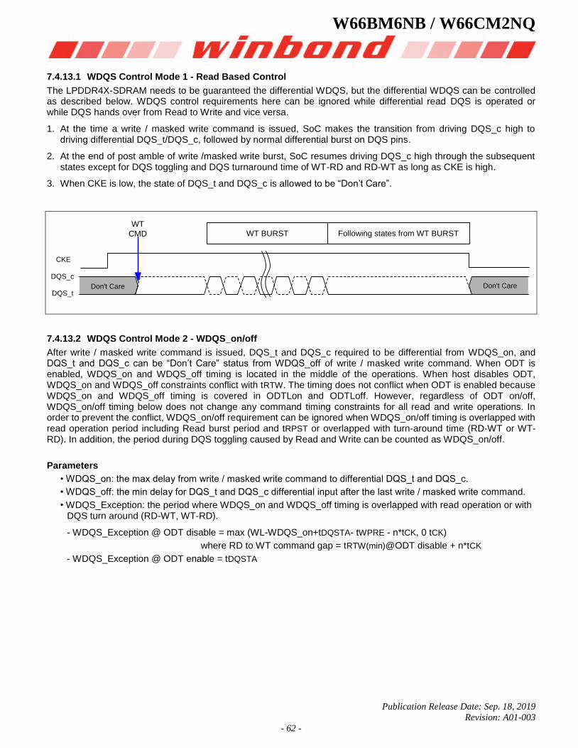
W66BM6NB / W66CM2NQ
Publication Release Date: Sep. 18, 2019
Revision: A01-003
- 62 -
7.4.13.1 WDQS Control Mode 1 - Read Based Control
The LPDDR4X-SDRAM needs to be guaranteed the differential WDQS, but the differential WDQS can be controlled as described below. WDQS control requirements here can be ignored while differential read DQS is operated or while DQS hands over from Read to Write and vice versa.
1. At the time a write / masked write command is issued, SoC makes the transition from driving DQS_c high to driving differential DQS_t/DQS_c, followed by normal differential burst on DQS pins.
2. At the end of post amble of write /masked write burst, SoC resumes driving DQS_c high through the subsequent states except for DQS toggling and DQS turnaround time of WT-RD and RD-WT as long as CKE is high.
3. When CKE is low, the state of DQS_t and DQS_c is allowed to be “Don’t Care”.
WT BURST Following states from WT BURSTWT
CMD
CKE
DQS_c
DQS_tDon't CareDon't Care
7.4.13.2 WDQS Control Mode 2 - WDQS_on/off
After write / masked write command is issued, DQS_t and DQS_c required to be differential from WDQS_on, and DQS_t and DQS_c can be “Don’t Care” status from WDQS_off of write / masked write command. When ODT is enabled, WDQS_on and WDQS_off timing is located in the middle of the operations. When host disables ODT, WDQS_on and WDQS_off constraints conflict with tRTW. The timing does not conflict when ODT is enabled because WDQS_on and WDQS_off timing is covered in ODTLon and ODTLoff. However, regardless of ODT on/off, WDQS_on/off timing below does not change any command timing constraints for all read and write operations. In order to prevent the conflict, WDQS_on/off requirement can be ignored when WDQS_on/off timing is overlapped with read operation period including Read burst period and tRPST or overlapped with turn-around time (RD-WT or WT-RD). In addition, the period during DQS toggling caused by Read and Write can be counted as WDQS_on/off.
Parameters
• WDQS_on: the max delay from write / masked write command to differential DQS_t and DQS_c.
• WDQS_off: the min delay for DQS_t and DQS_c differential input after the last write / masked write command.
• WDQS_Exception: the period where WDQS_on and WDQS_off timing is overlapped with read operation or with DQS turn around (RD-WT, WT-RD).
- WDQS_Exception @ ODT disable = max (WL-WDQS_on+tDQSTA- tWPRE - n*tCK, 0 tCK)
where RD to WT command gap = tRTW(min)@ODT disable + n*tCK
- WDQS_Exception @ ODT enable = tDQSTA
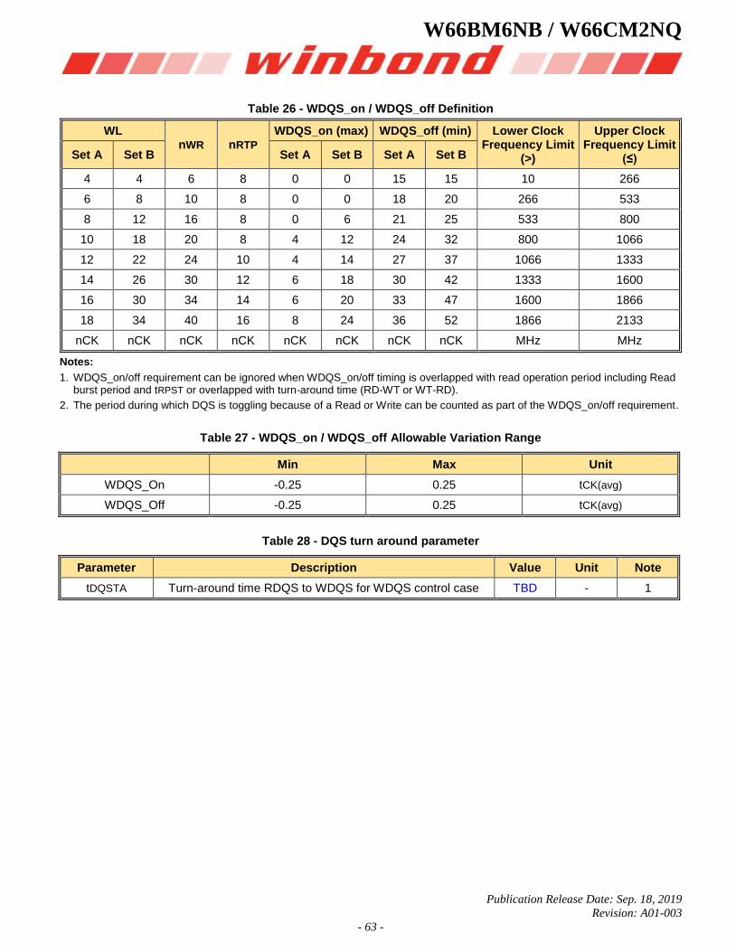
W66BM6NB / W66CM2NQ
Publication Release Date: Sep. 18, 2019
Revision: A01-003
- 63 -
Table 26 - WDQS_on / WDQS_off Definition
WL nWR nRTP
WDQS_on (max) WDQS_off (min) Lower Clock Frequency Limit
(>)
Upper Clock Frequency Limit
(≤) Set A Set B Set A Set B Set A Set B
4 4 6 8 0 0 15 15 10 266
6 8 10 8 0 0 18 20 266 533
8 12 16 8 0 6 21 25 533 800
10 18 20 8 4 12 24 32 800 1066
12 22 24 10 4 14 27 37 1066 1333
14 26 30 12 6 18 30 42 1333 1600
16 30 34 14 6 20 33 47 1600 1866
18 34 40 16 8 24 36 52 1866 2133
nCK nCK nCK nCK nCK nCK nCK nCK MHz MHz
Notes:
1. WDQS_on/off requirement can be ignored when WDQS_on/off timing is overlapped with read operation period including Read burst period and tRPST or overlapped with turn-around time (RD-WT or WT-RD).
2. The period during which DQS is toggling because of a Read or Write can be counted as part of the WDQS_on/off requirement.
Table 27 - WDQS_on / WDQS_off Allowable Variation Range
Min Max Unit
WDQS_On -0.25 0.25 tCK(avg)
WDQS_Off -0.25 0.25 tCK(avg)
Table 28 - DQS turn around parameter
Parameter Description Value Unit Note
tDQSTA Turn-around time RDQS to WDQS for WDQS control case TBD - 1
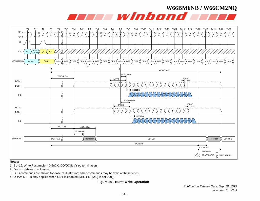
W66BM6NB / W66CM2NQ
Publication Release Date: Sep. 18, 2019
Revision: A01-003
- 64 -
T0 T1 T2 T3 Ta0 Ta1 Ta2 Ta3 Ta5 Ta6T4 Ta8 Ta9 Ta10 Ta11 Ta12 Ta13 Ta14 Ta15 Ta16 Ta17 Ta18 Ta19 Ta20 Ta21
CK_c
CK_t
Ta4
CS
CA CABLBA0,
CA, APCA
Write-1 CAS-2COMMAND
Din
n1
Din
n2
Din
n3
Din
n4
Din
n5
Din
n6
Din
n7
Din
n8
Din
n9
Din
n10
Din
n11
Din
n12
Din
n13
Din
n14
Din
n15
Din
n0
Din
n1
Din
n2
Din
n3
Din
n4
Din
n5
Din
n6
Din
n7
Din
n8
Din
n9
Din
n10
Din
n11
Din
n12
Din
n13
Din
n14
Din
n15
Din
n0
DES DES DES DES DES DES DES DES DES DES DES DES DES DES DES DES DES DES DES DES DES DES DES
WL
tWPRE
tWPRE tWPST
tWPST
tDQS2DQ
tDQSS (Min)
tDQSS (Max)
tDQS2DQ
WDQS_Off
WDQS_On
ODTLon tODTon.Max
tODTon.Min
ODTLoff
tODToff.Max
tODToff.Min
DQS_c
DQS_t
DQ
DQS_c
DQS_t
DQ
DRAM RTT
Ta7
TIME BREAKDON'T CARE
ODT Hi-Z ODTLonTransition Transition ODT Hi-Z
Notes:
1. BL=16, Write Postamble = 0.5nCK, DQ/DQS: VSSQ termination.
2. Din n = data-in to column n.
3. DES commands are shown for ease of illustration; other commands may be valid at these times.
4. DRAM RTT is only applied when ODT is enabled (MR11 OP[2:0] is not 000b).
Figure 26 - Burst Write Operation
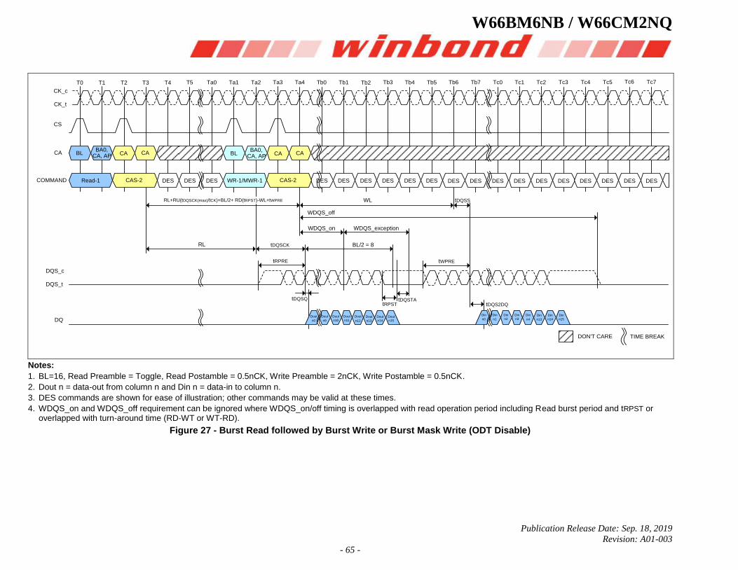
W66BM6NB / W66CM2NQ
Publication Release Date: Sep. 18, 2019
Revision: A01-003
- 65 -
tDQSQ
tDQSCK
tRPRE tWPRE
tDQSS
tRPST tDQS2DQ
BL/2 = 8RL
WLRL+RU(tDQSCK(max)/tCK)+BL/2+ RD(tRPST)-WL+tWPRE
CA CABLBA0,
CA, AP
Read-1 CAS-2 WR-1/MWR-1 CAS-2DES DES DES DES DES DES DES DES DES DES DES DES DES DES DES DES DES DES DES
CA CABLBA0,
CA, AP
T0 T1 T2 T3 T4 T5 Ta0 Ta1 Ta2 Ta3 Ta4 Tb0 Tb1 Tb2 Tb3 Tb4 Tb5 Tb6 Tb7 Tc0 Tc1 Tc2 Tc3 Tc4 Tc5 Tc6 Tc7
CK_c
CK_t
CS
CA
COMMAND
DQS_c
DQS_t
DQ
TIME BREAKDON'T CARE
Dout
n0
Dout
n9
Dout
n10
Dout
n11
Dout
n12
Dout
n13
Dout
n14
Dout
n15
Din
n0
Din
n1
Din
n2
Din
n3
Din
n4
Din
n13
Din
n14
Din
n15
tDQSTA
WDQS_on
WDQS_off
WDQS_exception
Notes:
1. BL=16, Read Preamble = Toggle, Read Postamble = 0.5nCK, Write Preamble = 2nCK, Write Postamble = 0.5nCK.
2. Dout n = data-out from column n and Din n = data-in to column n.
3. DES commands are shown for ease of illustration; other commands may be valid at these times.
4. WDQS_on and WDQS_off requirement can be ignored where WDQS_on/off timing is overlapped with read operation period including Read burst period and tRPST or overlapped with turn-around time (RD-WT or WT-RD).
Figure 27 - Burst Read followed by Burst Write or Burst Mask Write (ODT Disable)
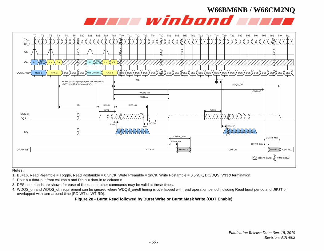
W66BM6NB / W66CM2NQ
Publication Release Date: Sep. 18, 2019
Revision: A01-003
- 66 -
CA CABLBA0,
CA, AP CA CABLBA0,
CA, AP
Read-1 CAS-2 WR-1/MWR-1 CAS-2DES DES DES DES DES DES DES DES DES DES DES DES DES DES DES DES DES DES DES DES DES DES DES DES DES
Dout n0
Dout n9
Dout n10
Dout n11
Dout n12
Dout n13
Dout n14
Dout n15
Dout n0
Dout n1
Dout n2
Dout n3
Dout n4
Dout n13
Dout n14
Dout n15
RL tDQSCK
tRPRE
tDQSQ
tRPST
tDQSTA
BL/2 = 8
ODTLon
WDQS_on
WL tDQSS
WDQS_Off
ODTLoff
tWPRE
ODToff_Max
ODToff_Min
ODTon_Max
ODTon_Min
tDQS2DQ
RL+RU(tDQSCK(max)/tCK)+BL/2+ RD(tRPST)
-ODTLon- RD(tODTon(min)/tCK)+1
TIME BREAKDON'T CARE
CK_c
CK_t
CS
CA
COMMAND
DQ
DQS_c
DQS_t
DRAM RTT
T0 T1 T2 T3 T4 T5 Ta0 Ta1 Ta2 Ta3 Ta4 Tb0 Tb1 Tb2 Tb3 Tb4 Tc0 Tc1 Tc2 Td0 Td1 Td2 Td3 Td4 Te0 Te1 Te2 Te3 Te4 Te5 Te6 Tf0 Tf1
Transition
TransitionODT Hi-Z ODT On ODT Hi-Z
Notes:
1. BL=16, Read Preamble = Toggle, Read Postamble = 0.5nCK, Write Preamble = 2nCK, Write Postamble = 0.5nCK, DQ/DQS: VSSQ termination.
2. Dout n = data-out from column n and Din n = data-in to column n.
3. DES commands are shown for ease of illustration; other commands may be valid at these times.
4. WDQS_on and WDQS_off requirement can be ignored where WDQS_on/off timing is overlapped with read operation period including Read burst period and tRPST or overlapped with turn-around time (RD-WT or WT-RD).
Figure 28 - Burst Read followed by Burst Write or Burst Mask Write (ODT Enable)
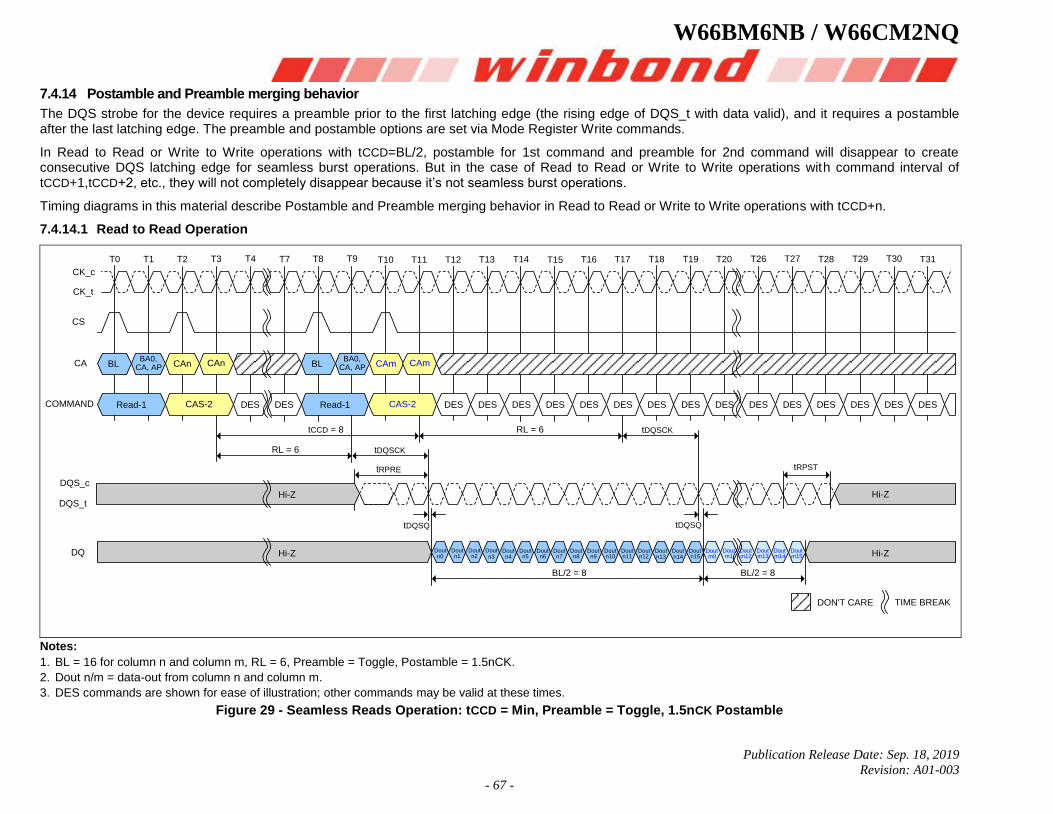
W66BM6NB / W66CM2NQ
Publication Release Date: Sep. 18, 2019
Revision: A01-003
- 67 -
7.4.14 Postamble and Preamble merging behavior
The DQS strobe for the device requires a preamble prior to the first latching edge (the rising edge of DQS_t with data valid), and it requires a postamble after the last latching edge. The preamble and postamble options are set via Mode Register Write commands.
In Read to Read or Write to Write operations with tCCD=BL/2, postamble for 1st command and preamble for 2nd command will disappear to create consecutive DQS latching edge for seamless burst operations. But in the case of Read to Read or Write to Write operations with command interval of tCCD+1,tCCD+2, etc., they will not completely disappear because it’s not seamless burst operations.
Timing diagrams in this material describe Postamble and Preamble merging behavior in Read to Read or Write to Write operations with tCCD+n.
7.4.14.1 Read to Read Operation
T0 T1 T2 T3 T4 T7 T8 T9 T10 T11 T12 T13 T14 T15 T16 T17 T18 T19 T20 T26 T27 T28 T29 T30 T31
CK_c
CK_t
BLCABA0,
CA, AP CAn CAn BLBA0,
CA, AP CAm CAm
Read-1COMMAND CAS-2 Read-1 CAS-2DES DES DES DES DES DES DES DES DES DES DES DES DES DES DES DES DES
Dout n0
Dout n1
Dout n2
Dout n3
Dout n4
Dout n5
Dout n6
Dout n7
Dout n8
Dout n9
Dout n10
Dout n11
Dout n12
Dout n13
Dout n14
Dout n15
Dout m0
Dout m1
Dout m12
Dout m13
Dout m14
Dout m15
CS
TIME BREAKDON'T CARE
DQ
DQS_c
DQS_t
tDQSQ tDQSQ
tDQSCK
tDQSCKtCCD = 8
tRPRE tRPST
BL/2 = 8BL/2 = 8
RL = 6
RL = 6
Hi-Z
Hi-Z
Hi-Z
Hi-Z
Notes:
1. BL = 16 for column n and column m, RL = 6, Preamble = Toggle, Postamble = 1.5nCK.
2. Dout n/m = data-out from column n and column m.
3. DES commands are shown for ease of illustration; other commands may be valid at these times.
Figure 29 - Seamless Reads Operation: tCCD = Min, Preamble = Toggle, 1.5nCK Postamble

W66BM6NB / W66CM2NQ
Publication Release Date: Sep. 18, 2019
Revision: A01-003
- 68 -
T0 T1 T2 T3 T4 T7 T8 T9 T10 T11 T12 T13 T14 T15 T16 T17 T18 T19 T20 T21 T26 T27 T28 T29 T30
CK_c
CK_t
BLCABA0,
CA, AP CAn CAn BLBA0,
CA, AP CAm CAm
Read-1COMMAND CAS-2 Read-1 CAS-2DES DES DES DES DES DES DES DES DES DES DES DES DES DES DES DES DES
Dout n0
Dout n1
Dout n2
Dout n3
Dout n4
Dout n5
Dout n6
Dout n7
Dout n8
Dout n9
Dout n10
Dout n11
Dout n12
Dout n13
Dout n14
Dout n15
Dout m0
Dout m1
Dout m12
Dout m13
Dout m14
Dout m15
CS
TIME BREAKDON'T CARE
DQ
DQS_c
DQS_t
tDQSQ tDQSQ
tDQSCK
tDQSCKtCCD = 9
tRPRE tRPST
BL/2 = 8BL/2 = 8
RL = 6
RL = 6
Hi-Z
Hi-Z
Hi-Z
Hi-Z
tRPST
Hi-Z
Notes:
1. BL = 16 for column n and column m, RL = 6, Preamble = Toggle, Postamble = 1.5nCK.
2. Dout n/m = data-out from column n and column m.
3. DES commands are shown for ease of illustration; other commands may be valid at these times.
Figure 30 - Consecutive Reads Operation: tCCD = Min +1, Preamble = Toggle, 1.5nCK Postamble

W66BM6NB / W66CM2NQ
Publication Release Date: Sep. 18, 2019
Revision: A01-003
- 69 -
T0 T1 T2 T3 T4 T7 T8 T9 T10 T11 T12 T13 T14 T15 T16 T17 T18 T19 T20 T21 T26 T27 T28 T29 T30
CK_c
CK_t
BLCABA0,
CA, AP CAn CAn BLBA0,
CA, AP CAm CAm
Read-1COMMAND CAS-2 Read-1 CAS-2DES DES DES DES DES DES DES DES DES DES DES DES DES DES DES DES DES
Dout n0
Dout n1
Dout n2
Dout n3
Dout n4
Dout n5
Dout n6
Dout n7
Dout n8
Dout n9
Dout n10
Dout n11
Dout n12
Dout n13
Dout n14
Dout n15
Dout m0
Dout m1
Dout m12
Dout m13
Dout m14
Dout m15
CS
TIME BREAKDON'T CARE
DQ
DQS_c
DQS_t
tDQSQ tDQSQ
tDQSCK
tDQSCKtCCD = 9
tRPRE
tRPST
BL/2 = 8BL/2 = 8
RL = 6
RL = 6
Hi-Z
Hi-Z Hi-Z
tRPST
Hi-Z
Hi-Z
tRPRE
Notes:
1. BL = 16 for column n and column m, RL = 6, Preamble = Toggle, Postamble = 0.5nCK.
2. Dout n/m = data-out from column n and column m.
3. DES commands are shown for ease of illustration; other commands may be valid at these times.
Figure 31 - Consecutive Reads Operation: tCCD = Min +1, Preamble = Toggle, 0.5nCK Postamble

W66BM6NB / W66CM2NQ
Publication Release Date: Sep. 18, 2019
Revision: A01-003
- 70 -
T0 T1 T2 T3 T4 T7 T8 T9 T10 T11 T12 T13 T14 T15 T16 T17 T18 T19 T20 T21 T26 T27 T28 T29 T30
CK_c
CK_t
BLCABA0,
CA, AP CAn CAn BLBA0,
CA, AP CAm CAm
Read-1COMMAND CAS-2 Read-1 CAS-2DES DES DES DES DES DES DES DES DES DES DES DES DES DES DES DES DES
Dout n0
Dout n1
Dout n2
Dout n3
Dout n4
Dout n5
Dout n6
Dout n7
Dout n8
Dout n9
Dout n10
Dout n11
Dout n12
Dout n13
Dout n14
Dout n15
Dout m0
Dout m1
Dout m12
Dout m13
Dout m14
Dout m15
CS
TIME BREAKDON'T CARE
DQ
DQS_c
DQS_t
tDQSQ tDQSQ
tDQSCK
tDQSCKtCCD = 9
tRPRE tRPST
BL/2 = 8BL/2 = 8
RL = 6
RL = 6
Hi-Z
Hi-Z
Hi-Z
Hi-Z
tRPST
Hi-Z
Notes:
1. BL = 16 for column n and column m, RL = 6, Preamble = Static, Postamble = 1.5nCK.
2. Dout n/m = data-out from column n and column m.
3. DES commands are shown for ease of illustration; other commands may be valid at these times.
Figure 32 - Consecutive Reads Operation: tCCD = Min +1, Preamble = Static, 1.5nCK Postamble

W66BM6NB / W66CM2NQ
Publication Release Date: Sep. 18, 2019
Revision: A01-003
- 71 -
T0 T1 T2 T3 T4 T7 T8 T9 T10 T11 T12 T13 T14 T15 T16 T17 T18 T19 T20 T21 T26 T27 T28 T29 T30
CK_c
CK_t
BLCABA0,
CA, AP CAn CAn BLBA0,
CA, AP CAm CAm
Read-1COMMAND CAS-2 Read-1 CAS-2DES DES DES DES DES DES DES DES DES DES DES DES DES DES DES DES DES
Dout n0
Dout n1
Dout n2
Dout n3
Dout n4
Dout n5
Dout n6
Dout n7
Dout n8
Dout n9
Dout n10
Dout n11
Dout n12
Dout n13
Dout n14
Dout n15
Dout m0
Dout m1
Dout m12
Dout m13
Dout m14
Dout m15
CS
TIME BREAKDON'T CARE
DQ
DQS_c
DQS_t
tDQSQ tDQSQ
tDQSCK
tDQSCKtCCD = 9
tRPREtRPST
BL/2 = 8BL/2 = 8
RL = 6
RL = 6
Hi-Z
Hi-Z Hi-Z Hi-Z
Hi-Z
tRPRE
Notes:
1. BL = 16 for column n and column m, RL = 6, Preamble = Static, Postamble = 0.5nCK.
2. Dout n/m = data-out from column n and column m.
3. DES commands are shown for ease of illustration; other commands may be valid at these times.
Figure 33 - Consecutive Reads Operation: tCCD = Min +1, Preamble = Static, 0.5nCK Postamble
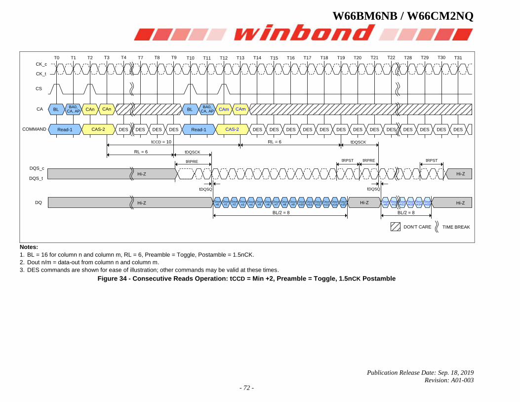
W66BM6NB / W66CM2NQ
Publication Release Date: Sep. 18, 2019
Revision: A01-003
- 72 -
T0 T1 T2 T3 T4 T7 T8 T9 T10 T11 T12 T13 T14 T15 T16 T17 T18 T19 T20 T21 T22 T28 T29 T30 T31
CK_c
CK_t
BLCABA0,
CA, AP CAn CAn BLBA0,
CA, AP CAm CAm
Read-1COMMAND CAS-2 Read-1 CAS-2DES DES DES DES DES DES DES DES DES DES DES DES DES DES DES DES DES
Dout n0
Dout n1
Dout n2
Dout n3
Dout n4
Dout n5
Dout n6
Dout n7
Dout n8
Dout n9
Dout n10
Dout n11
Dout n12
Dout n13
Dout n14
Dout n15
Dout m0
Dout m1
Dout m12
Dout m13
Dout m14
Dout m15
CS
TIME BREAKDON'T CARE
DQ
DQS_c
DQS_t
tDQSQ tDQSQ
tDQSCK
tDQSCKtCCD = 10
tRPRE tRPST
BL/2 = 8BL/2 = 8
RL = 6
RL = 6
Hi-Z
Hi-Z
tRPST
Hi-Z
tRPRE
Hi-Z
Hi-Z
Notes:
1. BL = 16 for column n and column m, RL = 6, Preamble = Toggle, Postamble = 1.5nCK.
2. Dout n/m = data-out from column n and column m.
3. DES commands are shown for ease of illustration; other commands may be valid at these times.
Figure 34 - Consecutive Reads Operation: tCCD = Min +2, Preamble = Toggle, 1.5nCK Postamble

W66BM6NB / W66CM2NQ
Publication Release Date: Sep. 18, 2019
Revision: A01-003
- 73 -
T0 T1 T2 T3 T4 T7 T8 T9 T10 T11 T12 T13 T14 T15 T16 T17 T18 T19 T20 T21 T22 T28 T29 T30 T31
CK_c
CK_t
BLCABA0,
CA, AP CAn CAn BLBA0,
CA, AP CAm CAm
Read-1COMMAND CAS-2 Read-1 CAS-2DES DES DES DES DES DES DES DES DES DES DES DES DES DES DES DES DES
Dout n0
Dout n1
Dout n2
Dout n3
Dout n4
Dout n5
Dout n6
Dout n7
Dout n8
Dout n9
Dout n10
Dout n11
Dout n12
Dout n13
Dout n14
Dout n15
Dout m0
Dout m1
Dout m12
Dout m13
Dout m14
Dout m15
CS
TIME BREAKDON'T CARE
DQ
DQS_c
DQS_t
tDQSQ tDQSQ
tDQSCK
tDQSCKtCCD = 10
tRPRE tRPST
BL/2 = 8BL/2 = 8
RL = 6
RL = 6
Hi-Z
Hi-Z
tRPST
Hi-Z
tRPRE
Hi-Z
Hi-Z
Notes:
1. BL = 16 for column n and column m, RL = 6, Preamble = Toggle, Postamble = 0.5nCK.
2. Dout n/m = data-out from column n and column m.
3. DES commands are shown for ease of illustration; other commands may be valid at these times.
Figure 35 - Consecutive Reads Operation: tCCD = Min +2, Preamble = Toggle, 0.5nCK Postamble
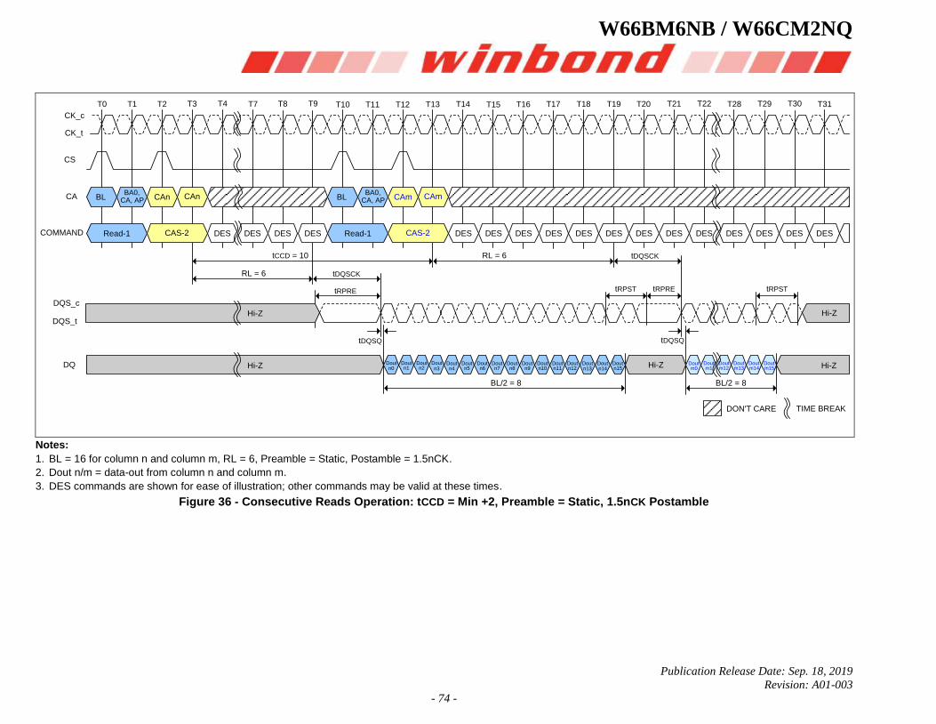
W66BM6NB / W66CM2NQ
Publication Release Date: Sep. 18, 2019
Revision: A01-003
- 74 -
T0 T1 T2 T3 T4 T7 T8 T9 T10 T11 T12 T13 T14 T15 T16 T17 T18 T19 T20 T21 T22 T28 T29 T30 T31
CK_c
CK_t
BLCABA0,
CA, AP CAn CAn BLBA0,
CA, AP CAm CAm
Read-1COMMAND CAS-2 Read-1 CAS-2DES DES DES DES DES DES DES DES DES DES DES DES DES DES DES DES DES
Dout n0
Dout n1
Dout n2
Dout n3
Dout n4
Dout n5
Dout n6
Dout n7
Dout n8
Dout n9
Dout n10
Dout n11
Dout n12
Dout n13
Dout n14
Dout n15
Dout m0
Dout m1
Dout m12
Dout m13
Dout m14
Dout m15
CS
TIME BREAKDON'T CARE
DQ
DQS_c
DQS_t
tDQSQ tDQSQ
tDQSCK
tDQSCKtCCD = 10
tRPRE tRPST
BL/2 = 8BL/2 = 8
RL = 6
RL = 6
Hi-Z
Hi-Z
tRPST
Hi-Z
tRPRE
Hi-Z
Hi-Z
Notes:
1. BL = 16 for column n and column m, RL = 6, Preamble = Static, Postamble = 1.5nCK.
2. Dout n/m = data-out from column n and column m.
3. DES commands are shown for ease of illustration; other commands may be valid at these times.
Figure 36 - Consecutive Reads Operation: tCCD = Min +2, Preamble = Static, 1.5nCK Postamble

W66BM6NB / W66CM2NQ
Publication Release Date: Sep. 18, 2019
Revision: A01-003
- 75 -
T0 T1 T2 T3 T4 T7 T8 T9 T10 T11 T12 T13 T14 T15 T16 T17 T18 T19 T20 T21 T22 T28 T29 T30 T31
CK_c
CK_t
BLCABA0,
CA, AP CAn CAn BLBA0,
CA, AP CAm CAm
Read-1COMMAND CAS-2 Read-1 CAS-2DES DES DES DES DES DES DES DES DES DES DES DES DES DES DES DES DES
Dout n0
Dout n1
Dout n2
Dout n3
Dout n4
Dout n5
Dout n6
Dout n7
Dout n8
Dout n9
Dout n10
Dout n11
Dout n12
Dout n13
Dout n14
Dout n15
Dout m0
Dout m1
Dout m12
Dout m13
Dout m14
Dout m15
CS
TIME BREAKDON'T CARE
DQ
DQS_c
DQS_t
tDQSQ tDQSQ
tDQSCK
tDQSCKtCCD = 10
tRPRE tRPST
BL/2 = 8BL/2 = 8
RL = 6
RL = 6
Hi-Z
Hi-Z
tRPST
Hi-Z
tRPRE
Hi-Z
Hi-Z
Notes:
1. BL = 16 for column n and column m, RL = 6, Preamble = Static, Postamble = 0.5nCK.
2. Dout n/m = data-out from column n and column m.
3. DES commands are shown for ease of illustration; other commands may be valid at these times.
Figure 37 - Consecutive Reads Operation: tCCD = Min +2, Preamble = Static, 0.5nCK Postamble
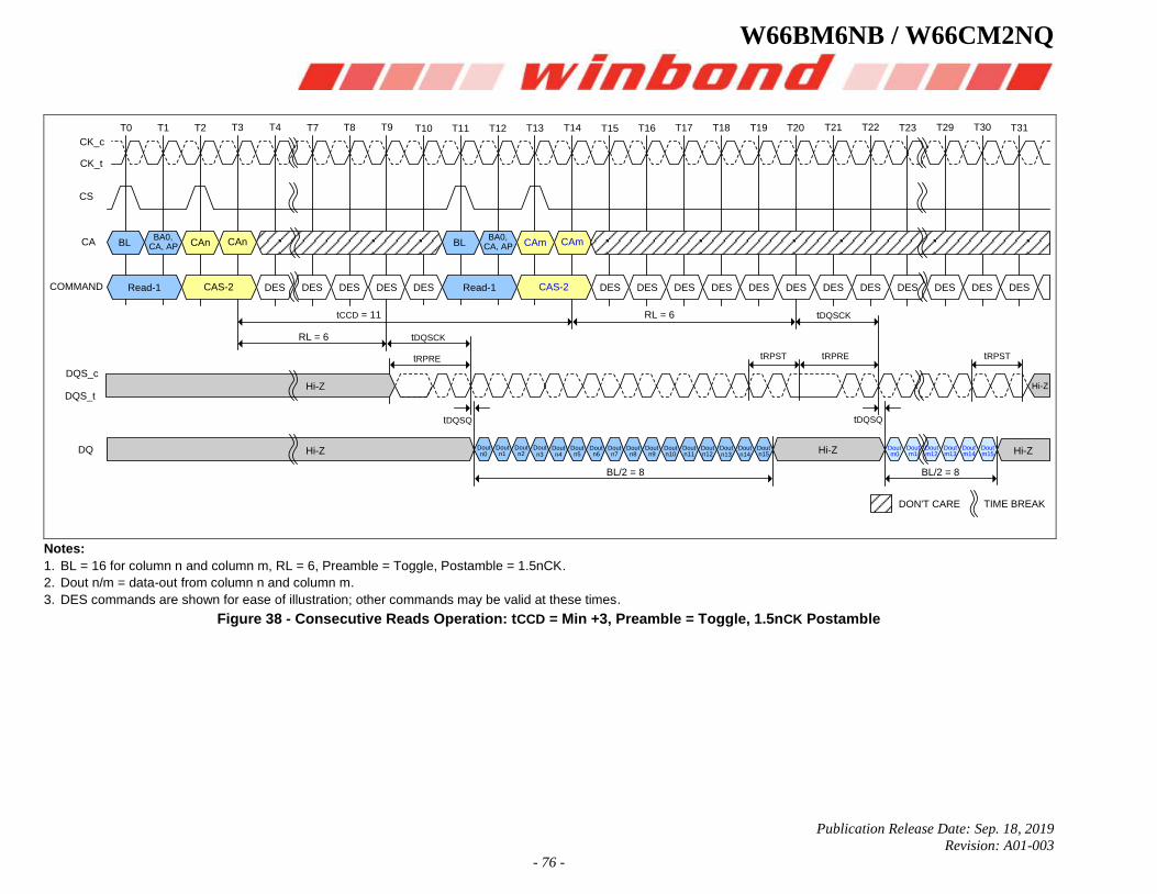
W66BM6NB / W66CM2NQ
Publication Release Date: Sep. 18, 2019
Revision: A01-003
- 76 -
T0 T1 T2 T3 T4 T7 T8 T9 T10 T11 T12 T13 T14 T15 T16 T17 T18 T19 T20 T21 T22 T23 T29 T30 T31
CK_c
CK_t
BLCABA0,
CA, AP CAn CAn BLBA0,
CA, AP CAm CAm
Read-1COMMAND CAS-2 Read-1 CAS-2DES DES DES DES DES DES DES DES DES DES DES DES DES DES DES DES DES
Dout n0
Dout n1
Dout n2
Dout n3
Dout n4
Dout n5
Dout n6
Dout n7
Dout n8
Dout n9
Dout n10
Dout n11
Dout n12
Dout n13
Dout n14
Dout n15
Dout m0
Dout m1
Dout m12
Dout m13
Dout m14
Dout m15
CS
TIME BREAKDON'T CARE
DQ
DQS_c
DQS_t
tDQSQ tDQSQ
tDQSCK
tDQSCKtCCD = 11
tRPRE tRPST
BL/2 = 8BL/2 = 8
RL = 6
RL = 6
Hi-Z
Hi-Z
tRPST tRPRE
Hi-Z
Hi-Z
Hi-Z
Notes:
1. BL = 16 for column n and column m, RL = 6, Preamble = Toggle, Postamble = 1.5nCK.
2. Dout n/m = data-out from column n and column m.
3. DES commands are shown for ease of illustration; other commands may be valid at these times.
Figure 38 - Consecutive Reads Operation: tCCD = Min +3, Preamble = Toggle, 1.5nCK Postamble
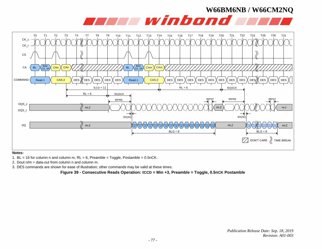
W66BM6NB / W66CM2NQ
Publication Release Date: Sep. 18, 2019
Revision: A01-003
- 77 -
T0 T1 T2 T3 T4 T7 T8 T9 T10 T11 T12 T13 T14 T15 T16 T17 T18 T19 T20 T21 T22 T23 T29 T30 T31
CK_c
CK_t
BLCABA0,
CA, AP CAn CAn BLBA0,
CA, AP CAm CAm
Read-1COMMAND CAS-2 Read-1 CAS-2DES DES DES DES DES DES DES DES DES DES DES DES DES DES DES DES DES
Dout n0
Dout n1
Dout n2
Dout n3
Dout n4
Dout n5
Dout n6
Dout n7
Dout n8
Dout n9
Dout n10
Dout n11
Dout n12
Dout n13
Dout n14
Dout n15
Dout m0
Dout m1
Dout m12
Dout m13
Dout m14
Dout m15
CS
TIME BREAKDON'T CARE
DQ
DQS_c
DQS_t
tDQSQ tDQSQ
tDQSCK
tDQSCKtCCD = 11
tRPRE tRPST
BL/2 = 8BL/2 = 8
RL = 6
RL = 6
Hi-Z
Hi-Z
tRPST tRPRE
Hi-Z Hi-Z
Hi-ZHi-Z
Notes:
1. BL = 16 for column n and column m, RL = 6, Preamble = Toggle, Postamble = 0.5nCK.
2. Dout n/m = data-out from column n and column m.
3. DES commands are shown for ease of illustration; other commands may be valid at these times.
Figure 39 - Consecutive Reads Operation: tCCD = Min +3, Preamble = Toggle, 0.5nCK Postamble
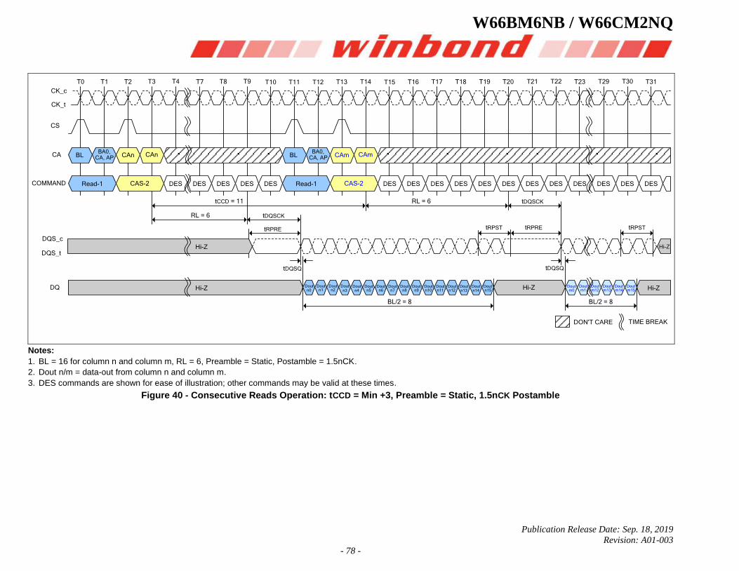
W66BM6NB / W66CM2NQ
Publication Release Date: Sep. 18, 2019
Revision: A01-003
- 78 -
T0 T1 T2 T3 T4 T7 T8 T9 T10 T11 T12 T13 T14 T15 T16 T17 T18 T19 T20 T21 T22 T23 T29 T30 T31
CK_c
CK_t
BLCABA0,
CA, AP CAn CAn BLBA0,
CA, AP CAm CAm
Read-1COMMAND CAS-2 Read-1 CAS-2DES DES DES DES DES DES DES DES DES DES DES DES DES DES DES DES DES
Dout n0
Dout n1
Dout n2
Dout n3
Dout n4
Dout n5
Dout n6
Dout n7
Dout n8
Dout n9
Dout n10
Dout n11
Dout n12
Dout n13
Dout n14
Dout n15
Dout m0
Dout m1
Dout m12
Dout m13
Dout m14
Dout m15
CS
TIME BREAKDON'T CARE
DQ
DQS_c
DQS_t
tDQSQ tDQSQ
tDQSCK
tDQSCKtCCD = 11
tRPRE tRPST
BL/2 = 8BL/2 = 8
RL = 6
RL = 6
Hi-Z
Hi-Z
tRPST tRPRE
Hi-Z
Hi-Z
Hi-Z
Notes:
1. BL = 16 for column n and column m, RL = 6, Preamble = Static, Postamble = 1.5nCK.
2. Dout n/m = data-out from column n and column m.
3. DES commands are shown for ease of illustration; other commands may be valid at these times.
Figure 40 - Consecutive Reads Operation: tCCD = Min +3, Preamble = Static, 1.5nCK Postamble

W66BM6NB / W66CM2NQ
Publication Release Date: Sep. 18, 2019
Revision: A01-003
- 79 -
T0 T1 T2 T3 T4 T7 T8 T9 T10 T11 T12 T13 T14 T15 T16 T17 T18 T19 T20 T21 T22 T23 T29 T30 T31
CK_c
CK_t
BLCABA0,
CA, AP CAn CAn BLBA0,
CA, AP CAm CAm
Read-1COMMAND CAS-2 Read-1 CAS-2DES DES DES DES DES DES DES DES DES DES DES DES DES DES DES DES DES
Dout n0
Dout n1
Dout n2
Dout n3
Dout n4
Dout n5
Dout n6
Dout n7
Dout n8
Dout n9
Dout n10
Dout n11
Dout n12
Dout n13
Dout n14
Dout n15
Dout m0
Dout m1
Dout m12
Dout m13
Dout m14
Dout m15
CS
TIME BREAKDON'T CARE
DQ
DQS_c
DQS_t
tDQSQ tDQSQ
tDQSCK
tDQSCKtCCD = 11
tRPRE tRPST
BL/2 = 8BL/2 = 8
RL = 6
RL = 6
Hi-Z
Hi-Z
tRPST tRPRE
Hi-Z Hi-Z
Hi-ZHi-Z
Notes:
1. BL = 16 for column n and column m, RL = 6, Preamble = Static, Postamble = 0.5nCK.
2. Dout n/m = data-out from column n and column m.
3. DES commands are shown for ease of illustration; other commands may be valid at these times.
Figure 41 - Consecutive Reads Operation: tCCD = Min +3, Preamble = Static, 0.5nCK Postamble
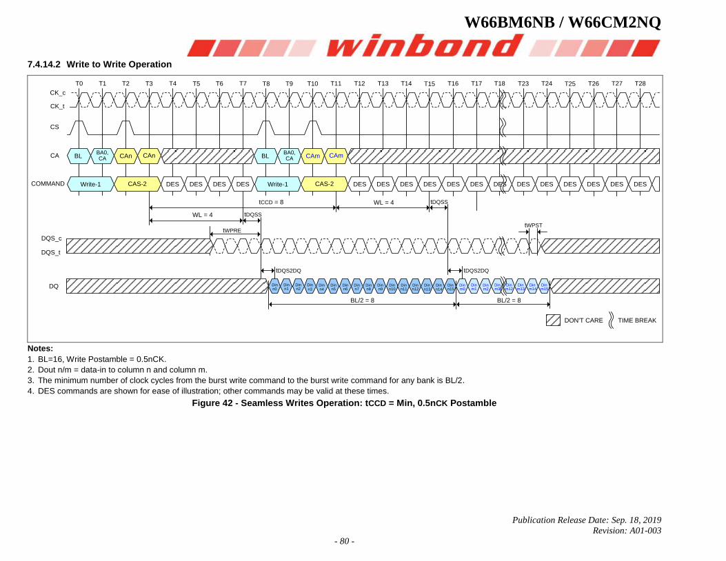
W66BM6NB / W66CM2NQ
Publication Release Date: Sep. 18, 2019
Revision: A01-003
- 80 -
7.4.14.2 Write to Write Operation
T0 T1 T2 T3 T4 T5 T6 T7 T8 T9 T10 T11 T12 T13 T14 T15 T16 T17 T18 T23 T24 T25 T26 T27 T28
CK_c
CK_t
BLCABA0,CA CAn CAn BL
BA0,CA CAm CAm
Write-1COMMAND CAS-2 Write-1 CAS-2DES DES DES DES DES DES DES DES DES DES DES DES DES DES DES DES DES
Din n0
Din n1
Din n2
Din n3
Din n4
Din n5
Din n6
Din n7
Din n8
Din n9
Din n10
Din n11
Din n12
Din n13
Din n14
Din n15
Din m0
Din m1
Din m12
Din m13
Din m14
Din m15
CS
TIME BREAKDON'T CARE
DQ
DQS_c
DQS_t
tDQS2DQ
tDQSS
tDQSStCCD = 8
tWPREtWPST
BL/2 = 8BL/2 = 8
WL = 4
WL = 4
Din m2
Din m3
tDQS2DQ
Notes:
1. BL=16, Write Postamble = 0.5nCK.
2. Dout n/m = data-in to column n and column m.
3. The minimum number of clock cycles from the burst write command to the burst write command for any bank is BL/2.
4. DES commands are shown for ease of illustration; other commands may be valid at these times.
Figure 42 - Seamless Writes Operation: tCCD = Min, 0.5nCK Postamble
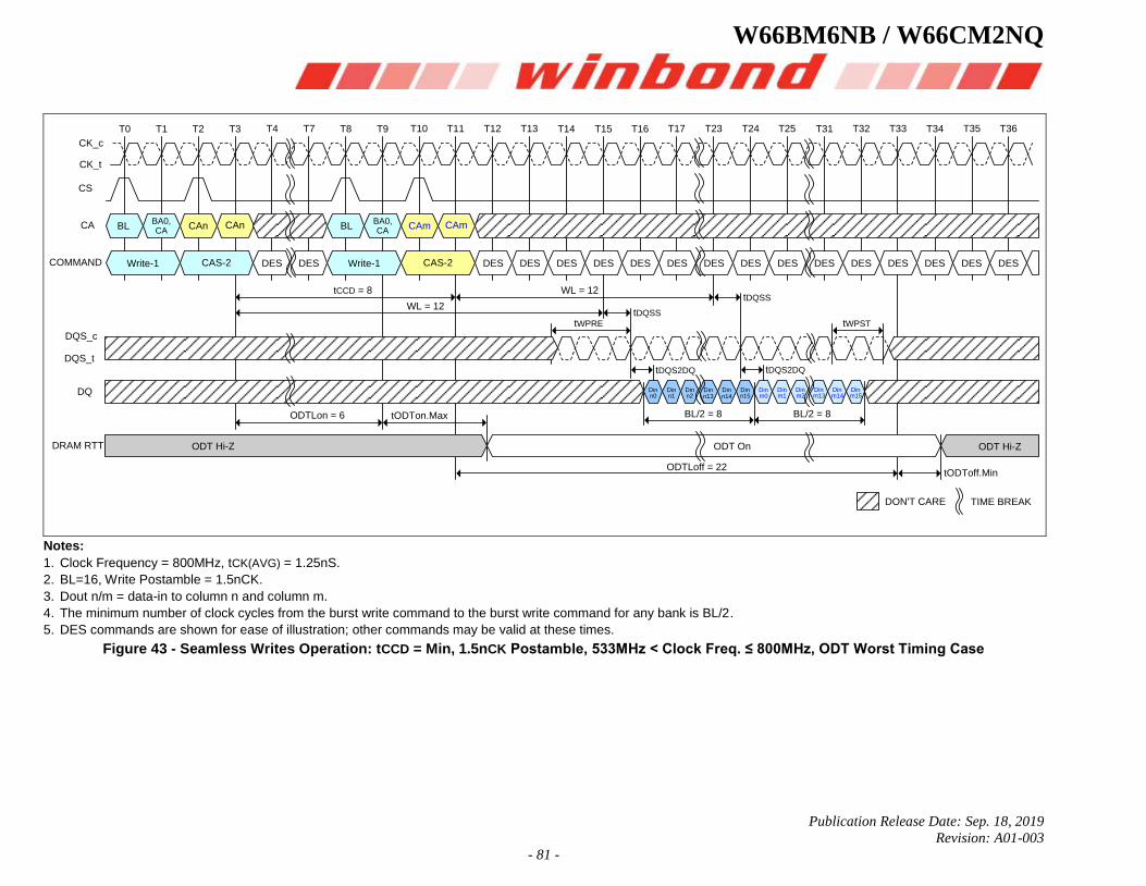
W66BM6NB / W66CM2NQ
Publication Release Date: Sep. 18, 2019
Revision: A01-003
- 81 -
T0 T1 T2 T3 T4 T7 T8 T9 T10 T11 T12 T13 T14 T15 T16 T17 T23 T24 T25 T31 T32 T33 T34 T35 T36
CK_c
CK_t
BLCA BA0,CA
CAn CAn BLBA0,CA
CAm CAm
Write-1COMMAND CAS-2 Write-1 CAS-2DES DES DES DES DES DES DES DES DES DES DES DES DES DES DES DES DES
Din n0
Din n1
Din n2
Din n13
Din n14
Din n15
Din m0
Din m1
Din m2
Din m13
Din m14
Din m15
CS
TIME BREAKDON'T CARE
DQ
DQS_c
DQS_ttDQS2DQ
tDQSStCCD = 8
tWPST
BL/2 = 8BL/2 = 8
WL = 12
WL = 12
tDQSS
tDQS2DQ
tWPRE
ODT Hi-ZODT Hi-Z ODT On
ODTLoff = 22tODToff.Min
ODTLon = 6 tODTon.Max
DRAM RTT
Notes:
1. Clock Frequency = 800MHz, tCK(AVG) = 1.25nS.
2. BL=16, Write Postamble = 1.5nCK.
3. Dout n/m = data-in to column n and column m.
4. The minimum number of clock cycles from the burst write command to the burst write command for any bank is BL/2.
5. DES commands are shown for ease of illustration; other commands may be valid at these times.
Figure 43 - Seamless Writes Operation: tCCD = Min, 1.5nCK Postamble, 533MHz < Clock Freq. ≤ 800MHz, ODT Worst Timing Case
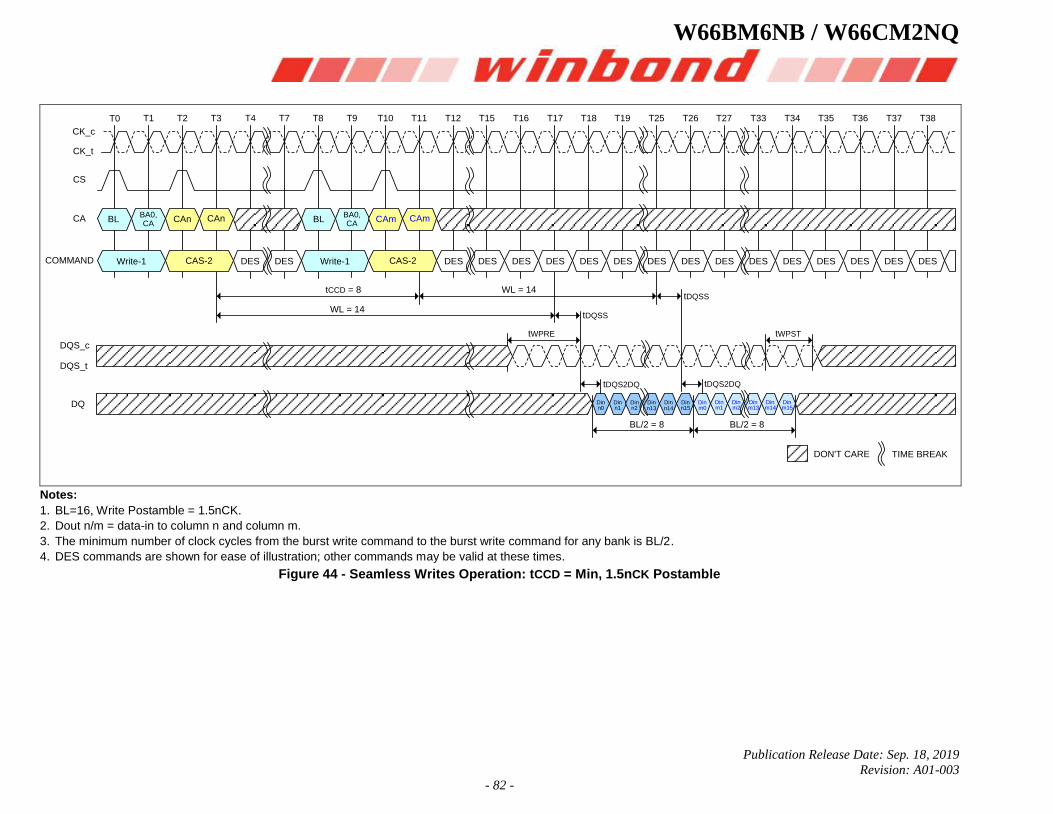
W66BM6NB / W66CM2NQ
Publication Release Date: Sep. 18, 2019
Revision: A01-003
- 82 -
T0 T1 T2 T3 T4 T7 T8 T9 T10 T11 T12 T15 T16 T17 T18 T19 T25 T26 T27 T33 T34 T35 T36 T37 T38
CK_c
CK_t
BLCA BA0,CA
CAn CAn BLBA0,CA
CAm CAm
Write-1COMMAND CAS-2 Write-1 CAS-2DES DES DES DES DES DES DES DES DES DES DES DES DES DES DES DES DES
Din n0
Din n1
Din n2
Din n13
Din n14
Din n15
Din m0
Din m1
Din m2
Din m13
Din m14
Din m15
CS
TIME BREAKDON'T CARE
DQ
DQS_c
DQS_t
tDQS2DQ
tDQSStCCD = 8
tWPST
BL/2 = 8BL/2 = 8
WL = 14
WL = 14
tDQSS
tDQS2DQ
tWPRE
Notes:
1. BL=16, Write Postamble = 1.5nCK.
2. Dout n/m = data-in to column n and column m.
3. The minimum number of clock cycles from the burst write command to the burst write command for any bank is BL/2.
4. DES commands are shown for ease of illustration; other commands may be valid at these times.
Figure 44 - Seamless Writes Operation: tCCD = Min, 1.5nCK Postamble

W66BM6NB / W66CM2NQ
Publication Release Date: Sep. 18, 2019
Revision: A01-003
- 83 -
T0 T1 T2 T3 T4 T8 T9 T10 T11 T12 T13 T14 T15 T16 T17 T23 T24 T25 T26 T32 T33 T34 T35 T36 T37
CK_c
CK_t
BLCA BA0,CA
CAn CAn BLBA0,CA
CAm CAm
Write-1COMMAND CAS-2 Write-1 CAS-2DES DES DES DES DES DES DES DES DES DES DES DES DES DES DES DES DES
Din n0
Din n1
Din n2
Din n13
Din n14
Din n15
Din m0
Din m1
Din m2
Din m13
Din m14
Din m15
CS
TIME BREAKDON'T CARE
DQ
DQS_c
DQS_t
tDQS2DQ
tDQSStCCD = 9
tWPST
BL/2 = 8BL/2 = 8
WL = 12
WL = 12
tDQSS
tDQS2DQ
tWPRE
Notes:
1. BL=16, Write Postamble = 0.5nCK.
2. Dout n/m = data-in to column n and column m.
3. DES commands are shown for ease of illustration; other commands may be valid at these times.
Figure 45 - Consecutive Writes Operation: tCCD = Min + 1, 0.5nCK Postamble
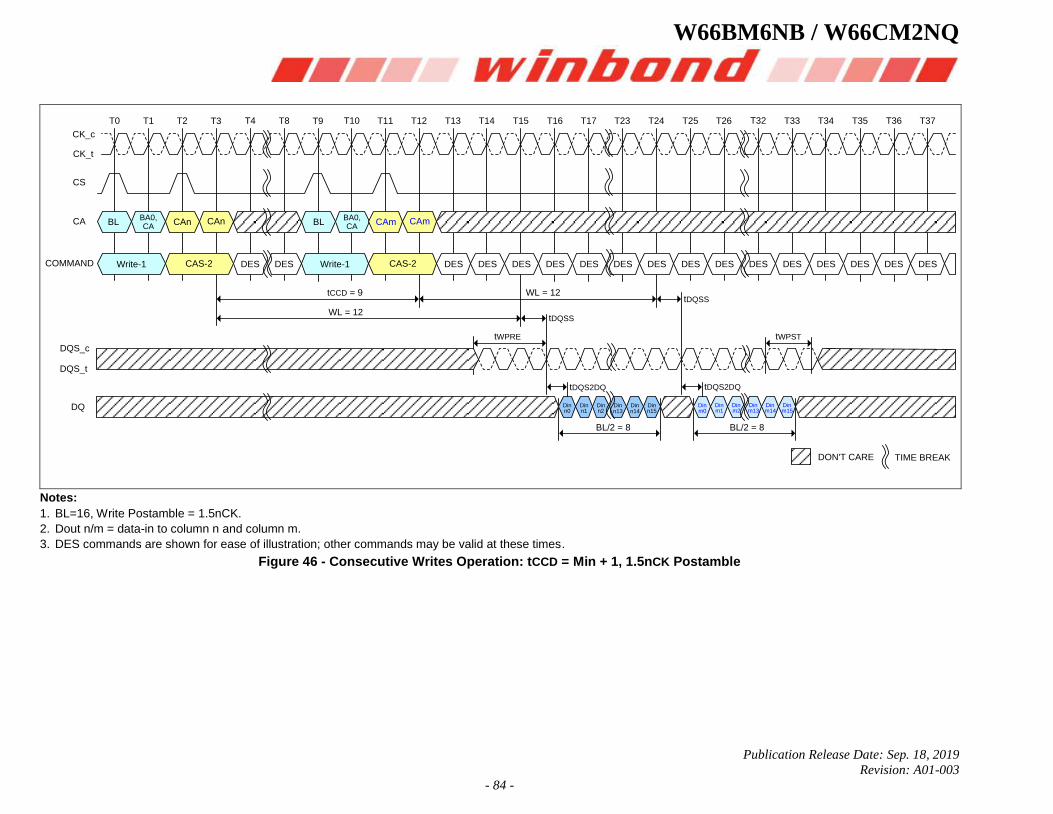
W66BM6NB / W66CM2NQ
Publication Release Date: Sep. 18, 2019
Revision: A01-003
- 84 -
CK_c
CK_t
BLCA BA0,CA
CAn CAn BLBA0,CA
CAm CAm
Write-1COMMAND CAS-2 Write-1 CAS-2DES DES DES DES DES DES DES DES DES DES DES DES DES DES DES DES DES
Din n0
Din n1
Din n2
Din n13
Din n14
Din n15
Din m0
Din m1
Din m2
Din m13
Din m14
Din m15
CS
DQ
DQS_c
DQS_t
tDQS2DQ
tDQSStCCD = 9
tWPST
BL/2 = 8BL/2 = 8
WL = 12
WL = 12
tDQSS
tDQS2DQ
tWPRE
TIME BREAKDON'T CARE
T0 T1 T2 T3 T4 T8 T9 T10 T11 T12 T13 T14 T15 T16 T17 T23 T24 T25 T26 T32 T33 T34 T35 T36 T37
Notes:
1. BL=16, Write Postamble = 1.5nCK.
2. Dout n/m = data-in to column n and column m.
3. DES commands are shown for ease of illustration; other commands may be valid at these times.
Figure 46 - Consecutive Writes Operation: tCCD = Min + 1, 1.5nCK Postamble

W66BM6NB / W66CM2NQ
Publication Release Date: Sep. 18, 2019
Revision: A01-003
- 85 -
T0 T1 T2 T3 T4 T9 T10 T11 T12 T13 T14 T15 T16 T17 T23 T24 T25 T26 T27 T33 T34 T35 T36 T37 T38
CK_c
CK_t
BLCA BA0,CA
CAn CAn BLBA0,CA
CAm CAm
Write-1COMMAND CAS-2 Write-1 CAS-2DES DES DES DES DES DES DES DES DES DES DES DES DES DES DES DES DES
Din n0
Din n1
Din n2
Din n13
Din n14
Din n15
Din m0
Din m1
Din m2
Din m13
Din m14
Din m15
CS
DQ
DQS_c
DQS_t
tDQS2DQ
tDQSStCCD = 10
tWPST
BL/2 = 8BL/2 = 8
WL = 12
WL = 12
tDQSS
tDQS2DQ
tWPRE tWPRE
tWPST
TIME BREAKDON'T CARE
Notes:
1. BL=16, Write Postamble = 0.5nCK.
2. Dout n/m = data-in to column n and column m.
3. DES commands are shown for ease of illustration; other commands may be valid at these times.
Figure 47 - Consecutive Writes Operation: tCCD = Min + 2, 0.5nCK Postamble
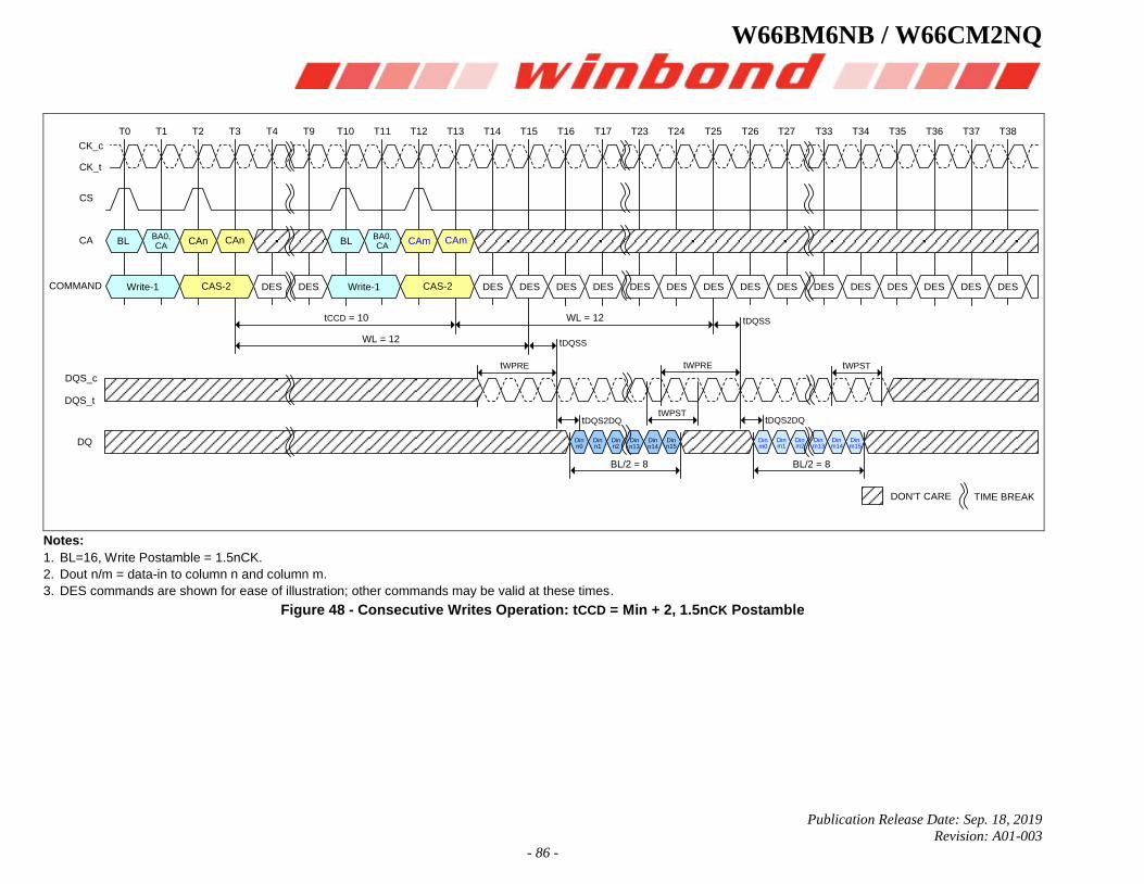
W66BM6NB / W66CM2NQ
Publication Release Date: Sep. 18, 2019
Revision: A01-003
- 86 -
T0 T1 T2 T3 T4 T9 T10 T11 T12 T13 T14 T15 T16 T17 T23 T24 T25 T26 T27 T33 T34 T35 T36 T37 T38
CK_c
CK_t
BLCA BA0,CA
CAn CAn BLBA0,CA
CAm CAm
Write-1COMMAND CAS-2 Write-1 CAS-2DES DES DES DES DES DES DES DES DES DES DES DES DES DES DES DES DES
Din n0
Din n1
Din n2
Din n13
Din n14
Din n15
Din m0
Din m1
Din m2
Din m13
Din m14
Din m15
CS
DQ
DQS_c
DQS_t
tDQS2DQ
tDQSStCCD = 10
tWPST
BL/2 = 8BL/2 = 8
WL = 12
WL = 12
tDQSS
tDQS2DQ
tWPRE tWPRE
tWPST
TIME BREAKDON'T CARE
Notes:
1. BL=16, Write Postamble = 1.5nCK.
2. Dout n/m = data-in to column n and column m.
3. DES commands are shown for ease of illustration; other commands may be valid at these times.
Figure 48 - Consecutive Writes Operation: tCCD = Min + 2, 1.5nCK Postamble

W66BM6NB / W66CM2NQ
Publication Release Date: Sep. 18, 2019
Revision: A01-003
- 87 -
T0 T1 T2 T3 T4 T9 T10 T11 T12 T13 T14 T15 T16 T17 T23 T24 T25 T26 T27 T28 T34 T35 T36 T37 T38
CK_c
CK_t
BLCA BA0,CA
CAn CAn BLBA0,CA
CAm CAm
Write-1COMMAND CAS-2 Write-1 CAS-2DES DES DES DES DES DES DES DES DES DES DES DES DES DES DES DES DES
Din n0
Din n1
Din n2
Din n13
Din n14
Din n15
Din m0
Din m1
Din m2
Din m13
Din m14
Din m15
CS
DQ
DQS_c
DQS_t
tDQS2DQ
tDQSStCCD = 11
tWPST
BL/2 = 8BL/2 = 8
WL = 12
WL = 12
tDQSS
tDQS2DQ
tWPRE tWPRE
tWPST
TIME BREAKDON'T CARE
Notes:
1. BL=16, Write Postamble = 0.5nCK.
2. Dout n/m = data-in to column n and column m.
3. DES commands are shown for ease of illustration; other commands may be valid at these times.
Figure 49 - Consecutive Writes Operation: tCCD = Min + 3, 0.5nCK Postamble
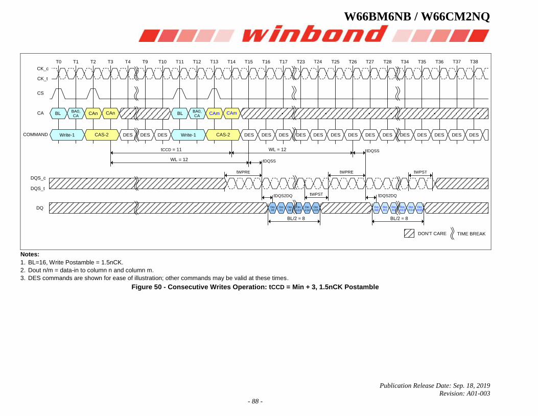
W66BM6NB / W66CM2NQ
Publication Release Date: Sep. 18, 2019
Revision: A01-003
- 88 -
T0 T1 T2 T3 T4 T9 T10 T11 T12 T13 T14 T15 T16 T17 T23 T24 T25 T26 T27 T28 T34 T35 T36 T37 T38
CK_c
CK_t
BLCA BA0,CA
CAn CAn BLBA0,CA
CAm CAm
Write-1COMMAND CAS-2 Write-1 CAS-2DES DES DES DES DES DES DES DES DES DES DES DES DES DES DES DES DES
Din n0
Din n1
Din n2
Din n13
Din n14
Din n15
Din m0
Din m1
Din m2
Din m13
Din m14
Din m15
CS
DQ
DQS_c
DQS_t
tDQS2DQ
tDQSStCCD = 11
tWPST
BL/2 = 8BL/2 = 8
WL = 12
WL = 12
tDQSS
tDQS2DQ
tWPRE tWPRE
tWPST
TIME BREAKDON'T CARE
Notes:
1. BL=16, Write Postamble = 1.5nCK.
2. Dout n/m = data-in to column n and column m.
3. DES commands are shown for ease of illustration; other commands may be valid at these times.
Figure 50 - Consecutive Writes Operation: tCCD = Min + 3, 1.5nCK Postamble

W66BM6NB / W66CM2NQ
Publication Release Date: Sep. 18, 2019
Revision: A01-003
- 89 -
T0 T1 T2 T3 T4 T9 T10 T11 T12 T13 T14 T15 T16 T17 T23 T24 T25 T26 T27 T28 T29 T35 T36 T37 T38
CK_c
CK_t
BLCA BA0,CA
CAn CAn BLBA0,CA
CAm CAm
Write-1COMMAND CAS-2 Write-1 CAS-2DES DES DES DES DES DES DES DES DES DES DES DES DES DES DES DES DES
Din n0
Din n1
Din n2
Din n13
Din n14
Din n15
Din m0
Din m1
Din m2
Din m13
Din m14
Din m15
CS
DQ
DQS_c
DQS_t
tDQS2DQ
tDQSStCCD = 12
tWPST
BL/2 = 8BL/2 = 8
WL = 12
WL = 12
tDQSS
tDQS2DQ
tWPRE tWPRE
tWPST
TIME BREAKDON'T CARE
Notes:
1. BL=16, Write Postamble = 1.5nCK.
2. Dout n/m = data-in to column n and column m.
3. DES commands are shown for ease of illustration; other commands may be valid at these times.
Figure 51 - Consecutive Writes Operation: tCCD = Min + 4, 1.5nCK Postamble
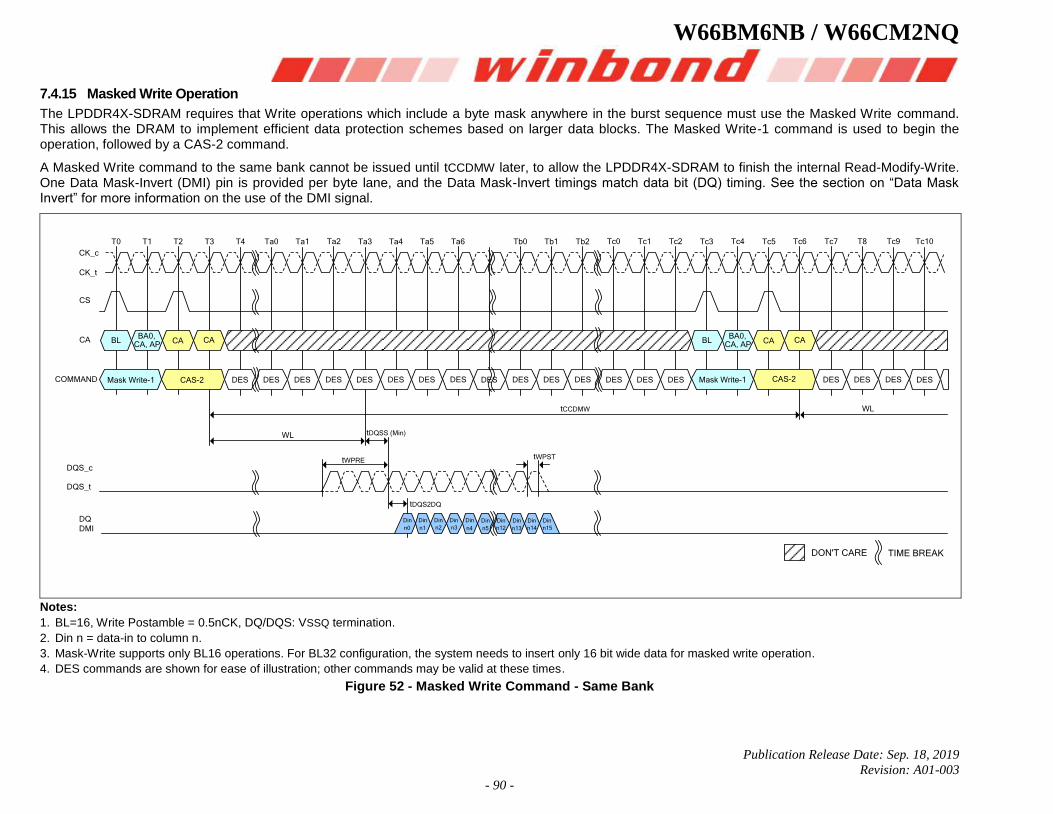
W66BM6NB / W66CM2NQ
Publication Release Date: Sep. 18, 2019
Revision: A01-003
- 90 -
7.4.15 Masked Write Operation
The LPDDR4X-SDRAM requires that Write operations which include a byte mask anywhere in the burst sequence must use the Masked Write command. This allows the DRAM to implement efficient data protection schemes based on larger data blocks. The Masked Write-1 command is used to begin the operation, followed by a CAS-2 command.
A Masked Write command to the same bank cannot be issued until tCCDMW later, to allow the LPDDR4X-SDRAM to finish the internal Read-Modify-Write. One Data Mask-Invert (DMI) pin is provided per byte lane, and the Data Mask-Invert timings match data bit (DQ) timing. See the section on “Data Mask Invert” for more information on the use of the DMI signal.
T0 T1 T2 T3 Ta0 Ta1 Ta2 Ta3 Ta5 Ta6T4 Tb0 Tb1 Tb2 Tc0 Tc1 Tc2 Tc3 Tc4 Tc5 Tc6 Tc7 T8 Tc9 Tc10
CK_c
CK_t
Ta4
CA CABLBA0,
CA, AP
CS
CA CA CABLBA0,
CA, AP
Mask Write-1 CAS-2 DES DES DES DES DES DES DES DES DES DES DES DES DESCOMMAND DES DES Mask Write-1 CAS-2 DES DES DES DES
tWPREDQS_c
DQS_t
tWPST
Din
n0
Din
n1
Din
n2
Din
n3
Din
n4
Din
n5
Din
n12
Din
n13
Din
n14
Din
n15
DQ
DMI
tDQS2DQ
tDQSS (Min)WL
tCCDMW WL
TIME BREAKDON'T CARE
Notes:
1. BL=16, Write Postamble = 0.5nCK, DQ/DQS: VSSQ termination.
2. Din n = data-in to column n.
3. Mask-Write supports only BL16 operations. For BL32 configuration, the system needs to insert only 16 bit wide data for masked write operation.
4. DES commands are shown for ease of illustration; other commands may be valid at these times.
Figure 52 - Masked Write Command - Same Bank
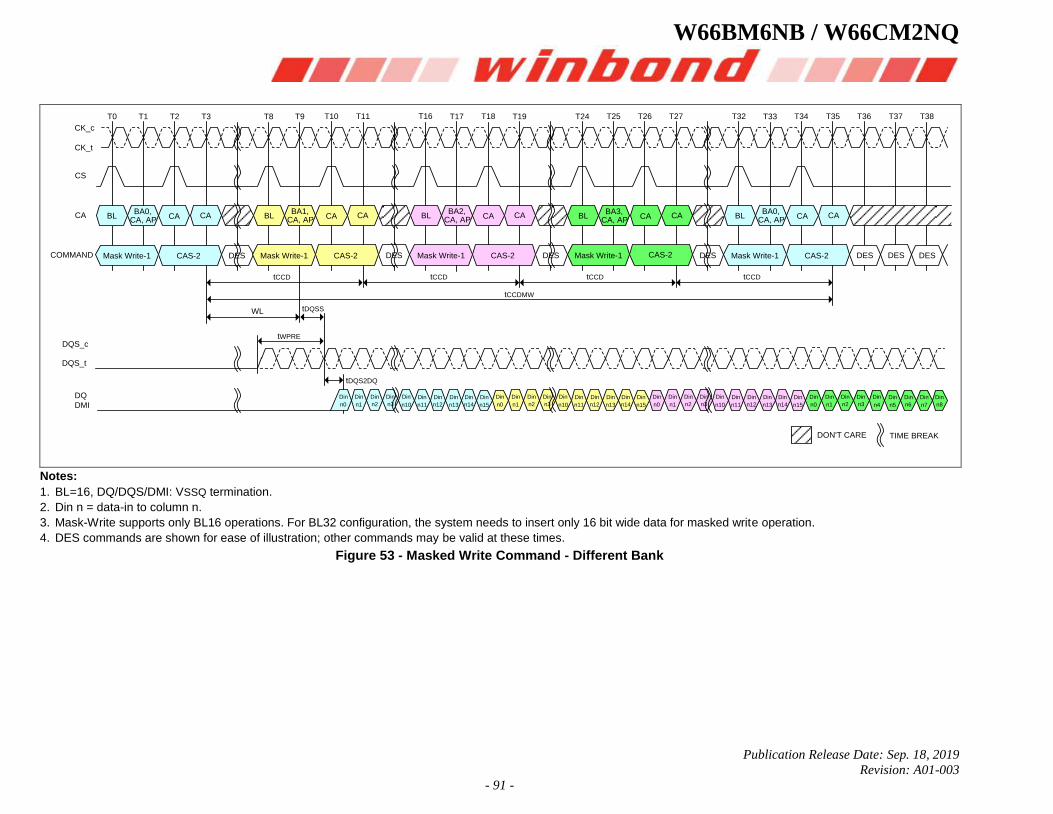
W66BM6NB / W66CM2NQ
Publication Release Date: Sep. 18, 2019
Revision: A01-003
- 91 -
T0 T1 T2 T3 T8 T9 T10 T11 T16 T17 T19 T24 T25 T26 T27 T32 T33 T34 T35 T36 T37 T38
CK_c
CK_t
T18
CA CABLBA0,
CA, AP
CS
CA CA CABLBA3,
CA, AP
Mask Write-1 CAS-2 DES DES DESCOMMAND Mask Write-1 CAS-2 DES DES DES DES
tWPREDQS_c
DQS_t
Din
n0
Din
n1
Din
n2
Din
n3
Din
n10
Din
n11
Din
n12
Din
n13
Din
n14
DQ
DMI
tDQS2DQ
tDQSSWL
TIME BREAKDON'T CARE
CA CABLBA1,
CA, AP
Mask Write-1 CAS-2
CA CABLBA2,
CA, AP
Mask Write-1 CAS-2
CA CABLBA0,
CA, AP
Mask Write-1 CAS-2
tCCD
tCCDMW
tCCD tCCD tCCD
Din
n15
Din
n0
Din
n1
Din
n2
Din
n3
Din
n10
Din
n11
Din
n12
Din
n13
Din
n14
Din
n15
Din
n0
Din
n1
Din
n2
Din
n3
Din
n10
Din
n11
Din
n12
Din
n13
Din
n14
Din
n15
Din
n0
Din
n1
Din
n2
Din
n3
Din
n4
Din
n5
Din
n6
Din
n7
Din
n8
Notes:
1. BL=16, DQ/DQS/DMI: VSSQ termination.
2. Din n = data-in to column n.
3. Mask-Write supports only BL16 operations. For BL32 configuration, the system needs to insert only 16 bit wide data for masked write operation.
4. DES commands are shown for ease of illustration; other commands may be valid at these times.
Figure 53 - Masked Write Command - Different Bank
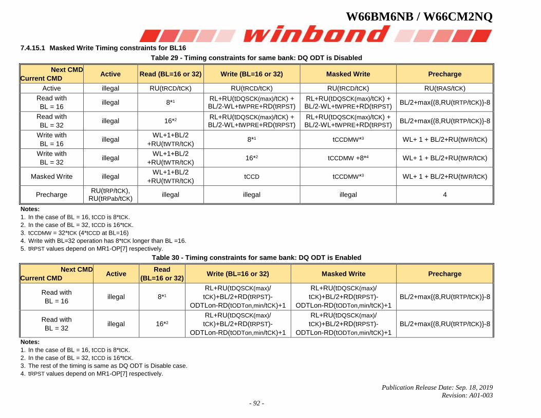
W66BM6NB / W66CM2NQ
Publication Release Date: Sep. 18, 2019
Revision: A01-003
- 92 -
7.4.15.1 Masked Write Timing constraints for BL16
Table 29 - Timing constraints for same bank: DQ ODT is Disabled
Next CMD
Current CMD Active Read (BL=16 or 32) Write (BL=16 or 32) Masked Write Precharge
Active illegal RU(tRCD/tCK) RU(tRCD/tCK) RU(tRCD/tCK) RU(tRAS/tCK)
Read with
BL = 16 illegal 8*1
RL+RU(tDQSCK(max)/tCK) + BL/2-WL+tWPRE+RD(tRPST)
RL+RU(tDQSCK(max)/tCK) + BL/2-WL+tWPRE+RD(tRPST)
BL/2+max{(8,RU(tRTP/tCK)}-8
Read with
BL = 32 illegal 16*2
RL+RU(tDQSCK(max)/tCK) + BL/2-WL+tWPRE+RD(tRPST)
RL+RU(tDQSCK(max)/tCK) + BL/2-WL+tWPRE+RD(tRPST)
BL/2+max{(8,RU(tRTP/tCK)}-8
Write with
BL = 16 illegal
WL+1+BL/2
+RU(tWTR/tCK) 8*1 tCCDMW*3 WL+ 1 + BL/2+RU(tWR/tCK)
Write with
BL = 32 illegal
WL+1+BL/2
+RU(tWTR/tCK) 16*2 tCCDMW +8*4 WL+ 1 + BL/2+RU(tWR/tCK)
Masked Write illegal WL+1+BL/2
+RU(tWTR/tCK) tCCD tCCDMW*3 WL+ 1 + BL/2+RU(tWR/tCK)
Precharge RU(tRP/tCK),
RU(tRPab/tCK) illegal illegal illegal 4
Notes:
1. In the case of BL = 16, tCCD is 8*tCK.
2. In the case of BL = 32, tCCD is 16*tCK.
3. tCCDMW = 32*tCK (4*tCCD at BL=16)
4. Write with BL=32 operation has 8*tCK longer than BL =16.
5. tRPST values depend on MR1-OP[7] respectively.
Table 30 - Timing constraints for same bank: DQ ODT is Enabled
Next CMD
Current CMD Active
Read
(BL=16 or 32) Write (BL=16 or 32) Masked Write Precharge
Read with
BL = 16 illegal 8*1
RL+RU(tDQSCK(max)/
tCK)+BL/2+RD(tRPST)-
ODTLon-RD(tODTon,min/tCK)+1
RL+RU(tDQSCK(max)/
tCK)+BL/2+RD(tRPST)-
ODTLon-RD(tODTon,min/tCK)+1
BL/2+max{(8,RU(tRTP/tCK)}-8
Read with
BL = 32 illegal 16*2
RL+RU(tDQSCK(max)/
tCK)+BL/2+RD(tRPST)-
ODTLon-RD(tODTon,min/tCK)+1
RL+RU(tDQSCK(max)/
tCK)+BL/2+RD(tRPST)-
ODTLon-RD(tODTon,min/tCK)+1
BL/2+max{(8,RU(tRTP/tCK)}-8
Notes:
1. In the case of BL = 16, tCCD is 8*tCK.
2. In the case of BL = 32, tCCD is 16*tCK.
3. The rest of the timing is same as DQ ODT is Disable case.
4. tRPST values depend on MR1-OP[7] respectively.
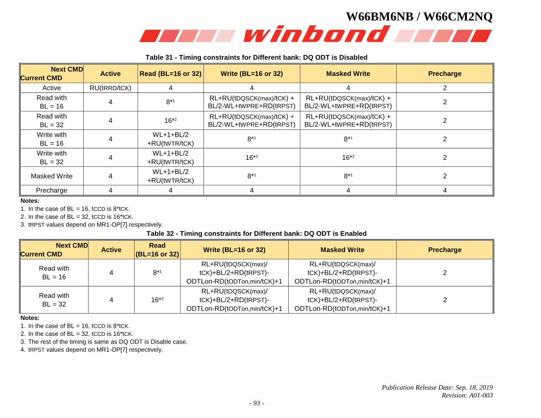
W66BM6NB / W66CM2NQ
Publication Release Date: Sep. 18, 2019
Revision: A01-003
- 93 -
Table 31 - Timing constraints for Different bank: DQ ODT is Disabled
Next CMD
Current CMD Active Read (BL=16 or 32) Write (BL=16 or 32) Masked Write Precharge
Active RU(tRRD/tCK) 4 4 4 2
Read with
BL = 16 4 8*1
RL+RU(tDQSCK(max)/tCK) + BL/2-WL+tWPRE+RD(tRPST)
RL+RU(tDQSCK(max)/tCK) + BL/2-WL+tWPRE+RD(tRPST)
2
Read with
BL = 32 4 16*2
RL+RU(tDQSCK(max)/tCK) + BL/2-WL+tWPRE+RD(tRPST)
RL+RU(tDQSCK(max)/tCK) + BL/2-WL+tWPRE+RD(tRPST)
2
Write with
BL = 16 4
WL+1+BL/2
+RU(tWTR/tCK) 8*1 8*1 2
Write with
BL = 32 4
WL+1+BL/2
+RU(tWTR/tCK) 16*2 16*2 2
Masked Write 4 WL+1+BL/2
+RU(tWTR/tCK) 8*1 8*1 2
Precharge 4 4 4 4 4
Notes:
1. In the case of BL = 16, tCCD is 8*tCK.
2. In the case of BL = 32, tCCD is 16*tCK.
3. tRPST values depend on MR1-OP[7] respectively.
Table 32 - Timing constraints for Different bank: DQ ODT is Enabled
Next CMD
Current CMD Active
Read
(BL=16 or 32) Write (BL=16 or 32) Masked Write Precharge
Read with
BL = 16 4 8*1
RL+RU(tDQSCK(max)/
tCK)+BL/2+RD(tRPST)-
ODTLon-RD(tODTon,min/tCK)+1
RL+RU(tDQSCK(max)/
tCK)+BL/2+RD(tRPST)-
ODTLon-RD(tODTon,min/tCK)+1
2
Read with
BL = 32 4 16*2
RL+RU(tDQSCK(max)/
tCK)+BL/2+RD(tRPST)-
ODTLon-RD(tODTon,min/tCK)+1
RL+RU(tDQSCK(max)/
tCK)+BL/2+RD(tRPST)-
ODTLon-RD(tODTon,min/tCK)+1
2
Notes:
1. In the case of BL = 16, tCCD is 8*tCK.
2. In the case of BL = 32, tCCD is 16*tCK.
3. The rest of the timing is same as DQ ODT is Disable case.
4. tRPST values depend on MR1-OP[7] respectively.
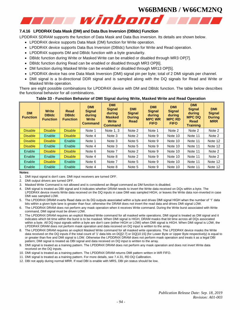
W66BM6NB / W66CM2NQ
Publication Release Date: Sep. 18, 2019
Revision: A01-003
- 94 -
7.4.16 LPDDR4X Data Mask (DM) and Data Bus Inversion (DBIdc) Function
LPDDR4X SDRAM supports the function of Data Mask and Data Bus inversion. Its details are shown below.
LPDDR4X device supports Data Mask (DM) function for Write operation.
LPDDR4X device supports Data Bus Inversion (DBIdc) function for Write and Read operation.
LPDDR4X supports DM and DBIdc function with a byte granularity.
DBIdc function during Write or Masked Write can be enabled or disabled through MR3 OP[7].
DBIdc function during Read can be enabled or disabled through MR3 OP[6].
DM function during Masked Write can be enabled or disabled through MR13 OP[5].
LPDDR4X device has one Data Mask Inversion (DMI) signal pin per byte; total of 2 DMI signals per channel.
DMI signal is a bi-directional DDR signal and is sampled along with the DQ signals for Read and Write or Masked Write operation.
There are eight possible combinations for LPDDR4X device with DM and DBIdc function. The table below describes the functional behavior for all combinations.
Table 33 - Function Behavior of DMI Signal during Write, Masked Write and Read Operation
DM Function
Write DBIdc
Function
Read DBIdc
Function
DMI Signal during Write
Command
DMI Signal during
Masked Write
Command
DMI Signal During Read
DMI Signal during
MPC WR FIFO
DMI Signal during
MPC RD FIFO
DMI Signal during
MPC DQ Read
Training
DMI Signal During MRR
Disable Disable Disable Note 1 Note 1, 3 Note 2 Note 1 Note 2 Note 2 Note 2
Disable Enable Disable Note 4 Note 3 Note 2 Note 9 Note 10 Note 11 Note 2
Disable Disable Enable Note 1 Note 3 Note 5 Note 9 Note 10 Note 11 Note 12
Disable Enable Enable Note 4 Note 3 Note 5 Note 9 Note 10 Note 11 Note 12
Enable Disable Disable Note 6 Note 7 Note 2 Note 9 Note 10 Note 11 Note 2
Enable Enable Disable Note 4 Note 8 Note 2 Note 9 Note 10 Note 11 Note 2
Enable Disable Enable Note 6 Note 7 Note 5 Note 9 Note 10 Note 11 Note 12
Enable Enable Enable Note 4 Note 8 Note 5 Note 9 Note 10 Note 11 Note 12
Notes:
1. DMI input signal is don't care. DMI input receivers are turned OFF.
2. DMI output drivers are turned OFF.
3. Masked Write Command is not allowed and is considered an illegal command as DM function is disabled.
4. DMI signal is treated as DBI signal and it indicates whether DRAM needs to invert the Write data received on DQs within a byte. The LPDDR4X device inverts Write data received on the DQ inputs in case DMI was sampled HIGH, or leaves the Write data non-inverted in case DMI was sampled LOW.
5. The LPDDR4X DRAM inverts Read data on its DQ outputs associated within a byte and drives DMI signal HIGH when the number of ‘1’ data bits within a given byte lane is greater than four; otherwise the DRAM does not invert the read data and drives DMI signal LOW.
6. The LPDDR4X DRAM does not perform any mask operation when it receives Write command. During the Write burst associated with Write command, DMI signal must be driven LOW.
7. The LPDDR4X DRAM requires an explicit Masked Write command for all masked write operations. DMI signal is treated as DM signal and it indicates which bit time within the burst is to be masked. When DMI signal is HIGH, DRAM masks that bit time across all DQs associated within a byte. All DQ input signals within a byte are don't care (either HIGH or LOW) when DMI signal is HIGH. When DMI signal is LOW, the LPDDR4X DRAM does not perform mask operation and data received on DQ input is written to the array.
8. The LPDDR4X DRAM requires an explicit Masked Write command for all masked write operations. The LPDDR4X device masks the Write data received on the DQ inputs if the total count of '1' data bits on DQ[2:7] or DQ[10:15] (for Lower Byte or Upper Byte respectively) is equal to or greater than five and DMI signal is LOW. Otherwise the LPDDR4X DRAM does not perform mask operation and treats it as a legal DBI pattern; DMI signal is treated as DBI signal and data received on DQ input is written to the array.
9. DMI signal is treated as a training pattern. The LPDDR4X DRAM does not perform any mask operation and does not invert Write data received on the DQ inputs.
10. DMI signal is treated as a training pattern. The LPDDR4X DRAM returns DMI pattern written in WR FIFO.
11. DMI signal is treated as a training pattern. For more details, see 7.4.31, RD DQ Calibration.
12. DBI not apply during normal MRR. If read DBI is enable with MRS, DBI pin status should be low.
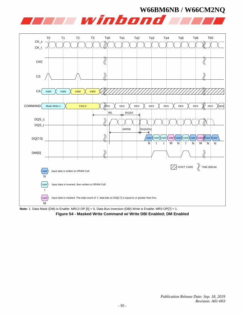
W66BM6NB / W66CM2NQ
Publication Release Date: Sep. 18, 2019
Revision: A01-003
- 95 -
T0 T1 T2 T3 Ta0 Ta1 Ta2 Ta3 Ta4 Ta5 Ta6 Tb0
N N N N NMMI I I
Valid Valid Valid Valid
DES DES DES DES DES DES DES DES DESMask Write-1 CAS-2
CS
CA
CK_c
CK_t
CKE
DQS_c
DQS_t
COMMAND
DQ[7:0]
DMI[0]
Valid2Valid1 Valid2 Valid3 Valid1 Valid2 Valid1 Valid3 Valid1 Valid1
I
Valid2
N
Valid1
M
Valid3
Input data is written to DRAM Cell.
Input data is inverted, then written to DRAM Cell.
Input data is masked. The total count of ‘1’ data bits on DQ[2:7] is equal to or greater than five.
DON'T CARE TIME BREAK
tDQS2DQtWPRE
tDQSSWL
Note: 1. Data Mask (DM) is Enable: MR13 OP [5] = 0, Data Bus Inversion (DBI) Write is Enable: MR3 OP[7] = 1.
Figure 54 - Masked Write Command w/ Write DBI Enabled; DM Enabled
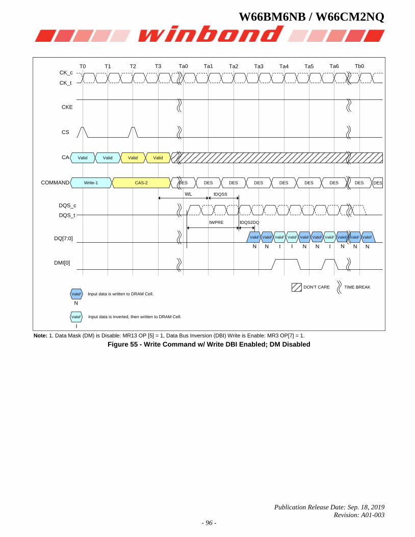
W66BM6NB / W66CM2NQ
Publication Release Date: Sep. 18, 2019
Revision: A01-003
- 96 -
T0 T1 T2 T3 Ta0 Ta1 Ta2 Ta3 Ta4 Ta5 Ta6 Tb0
N N I N NNIN I N
Valid Valid Valid Valid
DES DES DES DES DES DES DES DES DESWrite-1 CAS-2
CS
CA
CK_c
CK_t
CKE
DQS_c
DQS_t
COMMAND
DQ[7:0]
DMI[0]
Valid1Valid1 Valid2 Valid2 Valid1 Valid1 Valid2 Valid1 Valid1 Valid1
I
Valid2
N
Valid1 Input data is written to DRAM Cell.
Input data is inverted, then written to DRAM Cell.
DON'T CARE TIME BREAK
tDQS2DQtWPRE
tDQSSWL
Note: 1. Data Mask (DM) is Disable: MR13 OP [5] = 1, Data Bus Inversion (DBI) Write is Enable: MR3 OP[7] = 1.
Figure 55 - Write Command w/ Write DBI Enabled; DM Disabled
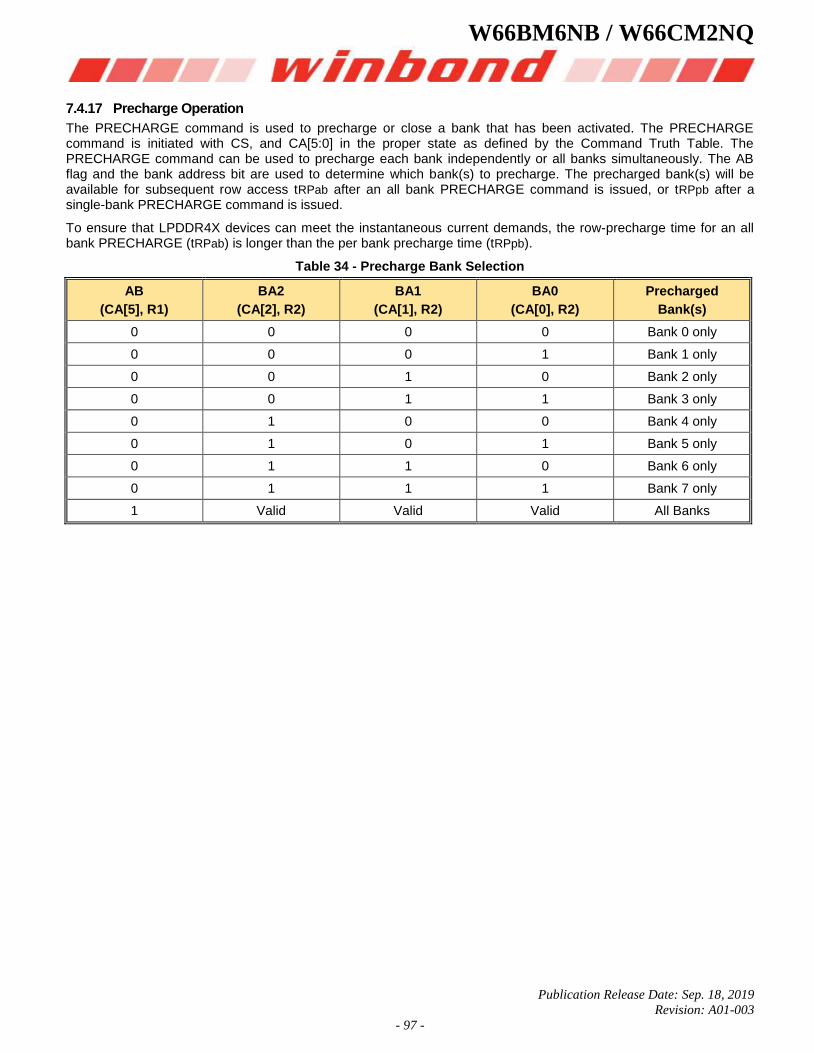
W66BM6NB / W66CM2NQ
Publication Release Date: Sep. 18, 2019
Revision: A01-003
- 97 -
7.4.17 Precharge Operation
The PRECHARGE command is used to precharge or close a bank that has been activated. The PRECHARGE command is initiated with CS, and CA[5:0] in the proper state as defined by the Command Truth Table. The PRECHARGE command can be used to precharge each bank independently or all banks simultaneously. The AB flag and the bank address bit are used to determine which bank(s) to precharge. The precharged bank(s) will be available for subsequent row access tRPab after an all bank PRECHARGE command is issued, or tRPpb after a single-bank PRECHARGE command is issued.
To ensure that LPDDR4X devices can meet the instantaneous current demands, the row-precharge time for an all bank PRECHARGE (tRPab) is longer than the per bank precharge time (tRPpb).
Table 34 - Precharge Bank Selection
AB
(CA[5], R1)
BA2
(CA[2], R2)
BA1
(CA[1], R2)
BA0
(CA[0], R2)
Precharged
Bank(s)
0 0 0 0 Bank 0 only
0 0 0 1 Bank 1 only
0 0 1 0 Bank 2 only
0 0 1 1 Bank 3 only
0 1 0 0 Bank 4 only
0 1 0 1 Bank 5 only
0 1 1 0 Bank 6 only
0 1 1 1 Bank 7 only
1 Valid Valid Valid All Banks
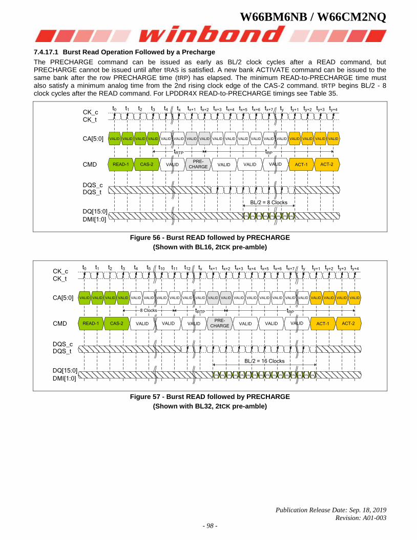
W66BM6NB / W66CM2NQ
Publication Release Date: Sep. 18, 2019
Revision: A01-003
- 98 -
7.4.17.1 Burst Read Operation Followed by a Precharge
The PRECHARGE command can be issued as early as BL/2 clock cycles after a READ command, but PRECHARGE cannot be issued until after tRAS is satisfied. A new bank ACTIVATE command can be issued to the same bank after the row PRECHARGE time (tRP) has elapsed. The minimum READ-to-PRECHARGE time must also satisfy a minimum analog time from the 2nd rising clock edge of the CAS-2 command. tRTP begins BL/2 - 8 clock cycles after the READ command. For LPDDR4X READ-to-PRECHARGE timings see Table 35.
t0 t1 t2 t3 t4 tx tx+1 tx+2 tx+3 tx+4 tx+5 tx+6 tx+7 ty ty+1 ty+2 ty+3 ty+4
VALID VALID VALID VALID VALID VALID VALID VALID VALID VALID VALID VALID VALID VALID VALID VALID VALID VALID
READ-1 CAS-2 VALID VALID VALIDPRE-
CHARGEVALID ACT-1 ACT-2
VAL VAL
CK_c
CK_t
CA[5:0]
CMD
DQS_cDQS_t
DQ[15:0]
DMI[1:0]
tRTP tRP
VAL VALVAL VAL VAL VAL
BL/2 = 8 Clocks
Figure 56 - Burst READ followed by PRECHARGE
(Shown with BL16, 2tCK pre-amble)
t0 t1 t2 t3 t4 t5 t10 t11 t12 tx tx+1 tx+2 tx+3 tx+4 tx+5 tx+6 tx+7 ty ty+1 ty+2 ty+3 ty+4
VALID VALID VALID VALID VALID VALID VALID VALID VALID VALID VALID VALID VALID VALID VALID VALID VALID VALID VALID VALID VALID VALID
READ-1 CAS-2 VALID VALID VALID VALID VALIDPRE-
CHARGEVALID ACT-1 ACT-2
VAL VALVAL VAL VAL VAL VAL VAL VAL VAL
CK_c
CK_t
CA[5:0]
CMD
DQS_cDQS_t
DQ[15:0]
DMI[1:0]
8 Clocks tRTP tRP
VAL VALVAL VAL VAL VAL
BL/2 = 16 Clocks
Figure 57 - Burst READ followed by PRECHARGE
(Shown with BL32, 2tCK pre-amble)
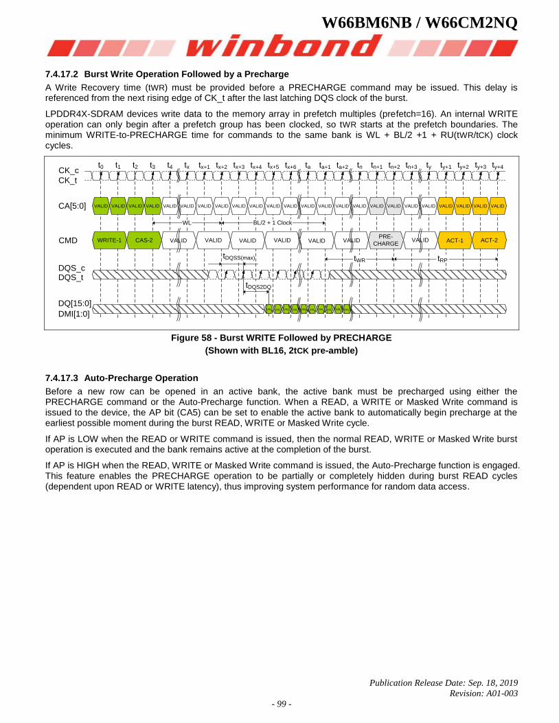
W66BM6NB / W66CM2NQ
Publication Release Date: Sep. 18, 2019
Revision: A01-003
- 99 -
7.4.17.2 Burst Write Operation Followed by a Precharge
A Write Recovery time (tWR) must be provided before a PRECHARGE command may be issued. This delay is referenced from the next rising edge of CK_t after the last latching DQS clock of the burst.
LPDDR4X-SDRAM devices write data to the memory array in prefetch multiples (prefetch=16). An internal WRITE operation can only begin after a prefetch group has been clocked, so tWR starts at the prefetch boundaries. The minimum WRITE-to-PRECHARGE time for commands to the same bank is WL + BL/2 +1 + RU(tWR/tCK) clock cycles.
t0 t1 t2 t3 t4 tx tx+1 tx+2 tx+3 tx+4 tx+5 tx+6 ta ta+1 ta+2 tn tn+1 tn+2 tn+3 ty ty+1 ty+2 ty+3 ty+4
VALID VALID VALID VALID VALID VALID VALID VALID VALID VALID VALID VALID VALID VALID VALID VALID VALID VALID VALID VALID VALID VALID VALID VALID
WRITE-1 CAS-2 VALID VALID VALID VALID VALID VALIDPRE-
CHARGEVALID ACT-1 ACT-2
VAL VALVAL VAL VAL VAL VAL VAL VAL VAL
CK_c
CK_t
CA[5:0]
CMD
DQS_cDQS_t
DQ[15:0]
DMI[1:0]
WL BL/2 + 1 Clock
tDQSS(max)
tDQS2DQ
tWR tRP
Figure 58 - Burst WRITE Followed by PRECHARGE
(Shown with BL16, 2tCK pre-amble)
7.4.17.3 Auto-Precharge Operation
Before a new row can be opened in an active bank, the active bank must be precharged using either the PRECHARGE command or the Auto-Precharge function. When a READ, a WRITE or Masked Write command is issued to the device, the AP bit (CA5) can be set to enable the active bank to automatically begin precharge at the earliest possible moment during the burst READ, WRITE or Masked Write cycle.
If AP is LOW when the READ or WRITE command is issued, then the normal READ, WRITE or Masked Write burst operation is executed and the bank remains active at the completion of the burst.
If AP is HIGH when the READ, WRITE or Masked Write command is issued, the Auto-Precharge function is engaged. This feature enables the PRECHARGE operation to be partially or completely hidden during burst READ cycles (dependent upon READ or WRITE latency), thus improving system performance for random data access.
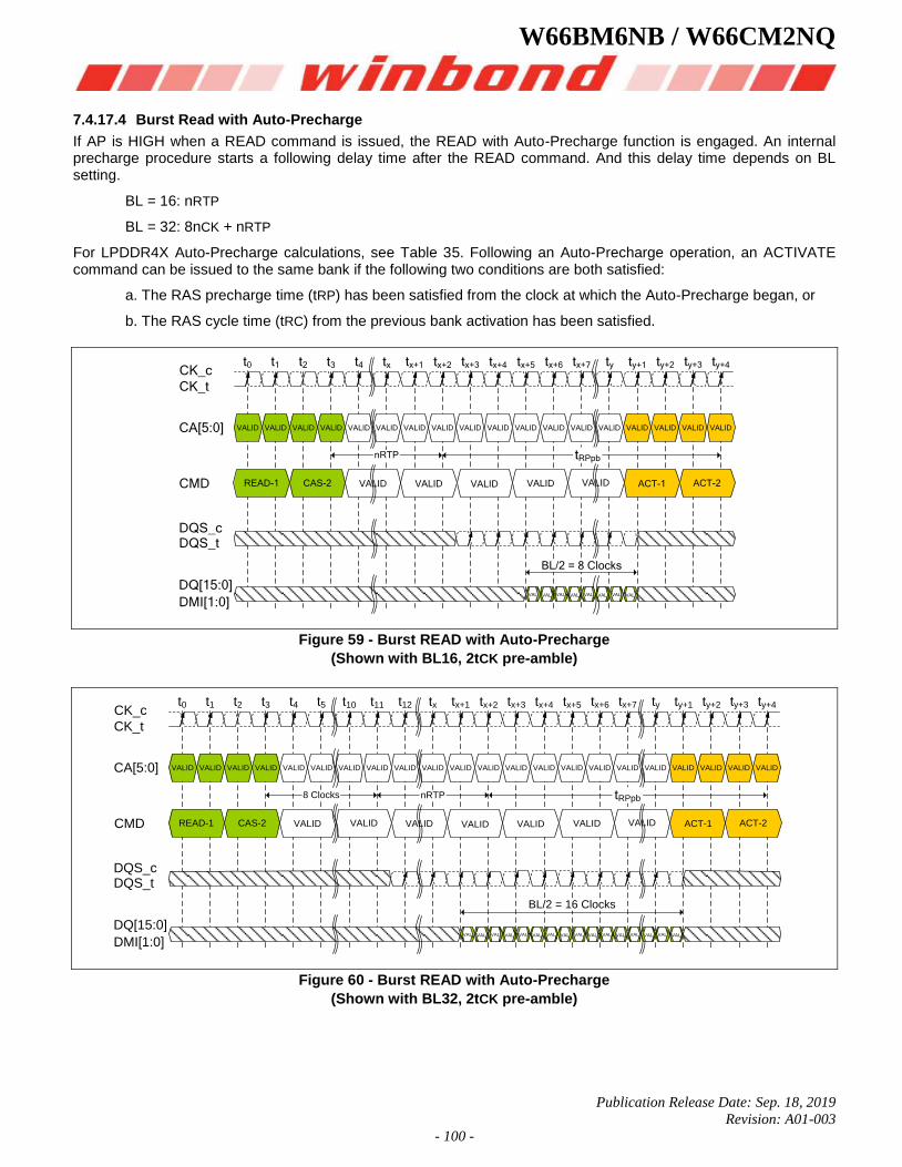
W66BM6NB / W66CM2NQ
Publication Release Date: Sep. 18, 2019
Revision: A01-003
- 100 -
7.4.17.4 Burst Read with Auto-Precharge
If AP is HIGH when a READ command is issued, the READ with Auto-Precharge function is engaged. An internal precharge procedure starts a following delay time after the READ command. And this delay time depends on BL setting.
BL = 16: nRTP
BL = 32: 8nCK + nRTP
For LPDDR4X Auto-Precharge calculations, see Table 35. Following an Auto-Precharge operation, an ACTIVATE command can be issued to the same bank if the following two conditions are both satisfied:
a. The RAS precharge time (tRP) has been satisfied from the clock at which the Auto-Precharge began, or
b. The RAS cycle time (tRC) from the previous bank activation has been satisfied.
t0 t1 t2 t3 t4 tx tx+1 tx+2 tx+3 tx+4 tx+5 tx+6 tx+7 ty ty+1 ty+2 ty+3 ty+4
VALID VALID VALID VALID VALID VALID VALID VALID VALID VALID VALID VALID VALID VALID VALID VALID VALID VALID
READ-1 CAS-2 VALID VALID VALID VALID ACT-1 ACT-2
VAL VAL
CK_c
CK_t
CA[5:0]
CMD
DQS_cDQS_t
DQ[15:0]
DMI[1:0]
nRTP tRPpb
VAL VALVAL VAL VAL VAL
BL/2 = 8 Clocks
VALID
Figure 59 - Burst READ with Auto-Precharge
(Shown with BL16, 2tCK pre-amble)
t0 t1 t2 t3 t4 t5 t10 t11 t12 tx tx+1 tx+2 tx+3 tx+4 tx+5 tx+6 tx+7 ty ty+1 ty+2 ty+3 ty+4
VALID VALID VALID VALID VALID VALID VALID VALID VALID VALID VALID VALID VALID VALID VALID VALID VALID VALID VALID VALID VALID VALID
READ-1 CAS-2 VALID VALID VALID VALID VALID VALID ACT-1 ACT-2
VAL VALVAL VAL VAL VAL VAL VAL VAL VAL
CK_c
CK_t
CA[5:0]
CMD
DQS_cDQS_t
DQ[15:0]
DMI[1:0]
8 Clocks tRPpb
VAL VALVAL VAL VAL VAL
BL/2 = 16 Clocks
nRTP
VALID
Figure 60 - Burst READ with Auto-Precharge
(Shown with BL32, 2tCK pre-amble)
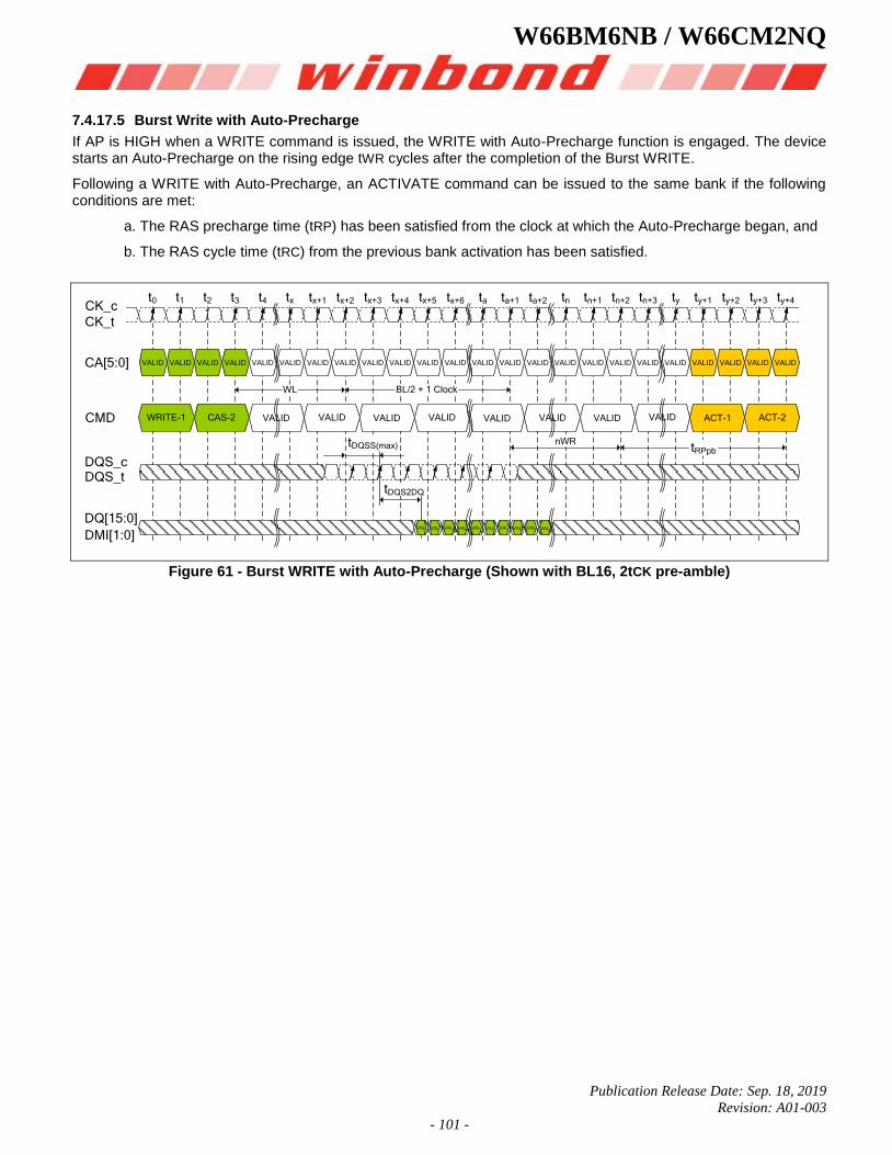
W66BM6NB / W66CM2NQ
Publication Release Date: Sep. 18, 2019
Revision: A01-003
- 101 -
7.4.17.5 Burst Write with Auto-Precharge
If AP is HIGH when a WRITE command is issued, the WRITE with Auto-Precharge function is engaged. The device starts an Auto-Precharge on the rising edge tWR cycles after the completion of the Burst WRITE.
Following a WRITE with Auto-Precharge, an ACTIVATE command can be issued to the same bank if the following conditions are met:
a. The RAS precharge time (tRP) has been satisfied from the clock at which the Auto-Precharge began, and
b. The RAS cycle time (tRC) from the previous bank activation has been satisfied.
t0 t1 t2 t3 t4 tx tx+1 tx+2 tx+3 tx+4 tx+5 tx+6 ta ta+1 ta+2 tn tn+1 tn+2 tn+3 ty ty+1 ty+2 ty+3 ty+4
VALID VALID VALID VALID VALID VALID VALID VALID VALID VALID VALID VALID VALID VALID VALID VALID VALID VALID VALID VALID VALID VALID VALID VALID
WRITE-1 CAS-2 VALID VALID VALID VALID VALID VALID VALID ACT-1 ACT-2
VAL VALVAL VAL VAL VAL VAL VAL VAL VAL
CK_c
CK_t
CA[5:0]
CMD
DQS_cDQS_t
DQ[15:0]
DMI[1:0]
WL BL/2 + 1 Clock
tDQSS(max)
tDQS2DQ
tRPpb
VALID
nWR
Figure 61 - Burst WRITE with Auto-Precharge (Shown with BL16, 2tCK pre-amble)
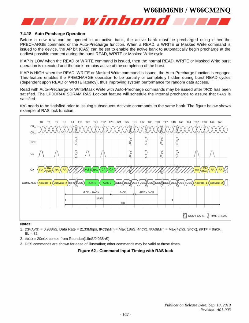
W66BM6NB / W66CM2NQ
Publication Release Date: Sep. 18, 2019
Revision: A01-003
- 102 -
7.4.18 Auto-Precharge Operation
Before a new row can be opened in an active bank, the active bank must be precharged using either the PRECHARGE command or the Auto-Precharge function. When a READ, a WRITE or Masked Write command is issued to the device, the AP bit (CA5) can be set to enable the active bank to automatically begin precharge at the earliest possible moment during the burst READ, WRITE or Masked Write cycle.
If AP is LOW when the READ or WRITE command is issued, then the normal READ, WRITE or Masked Write burst operation is executed and the bank remains active at the completion of the burst.
If AP is HIGH when the READ, WRITE or Masked Write command is issued, the Auto-Precharge function is engaged. This feature enables the PRECHARGE operation to be partially or completely hidden during burst READ cycles (dependent upon READ or WRITE latency), thus improving system performance for random data access.
Read with Auto-Precharge or Write/Mask Write with Auto-Precharge commands may be issued after tRCD has been satisfied. The LPDDR4X SDRAM RAS Lockout feature will schedule the internal precharge to assure that tRAS is satisfied.
tRC needs to be satisfied prior to issuing subsequent Activate commands to the same bank. The figure below shows example of RAS lock function.
CK_c
CK_t
CKE
CS
CA
COMMAND
T0
tRAS
tRC
tRCD = 20nCK
T1 T2 T3 T19 T20 T21 T22 T24 T25 T31 T32 Ta0 Ta1 Ta2 Ta3 Ta4 Ta5T39 T47
RA RA RABA0RA
Valid CA CABA0 RA RA RABA0RA
Activate -1 Activate -2 DES Activate -1 Activate -2DES RDA-1 CAS-2
TIME BREAKDON'T CARE
T4 T23 T38 T48
DES DES DES DES DES DES DES DES DES DES
8nCK nRTP = 8nCK
Notes:
1. tCK(AVG) = 0.938nS, Data Rate = 2133Mbps, tRCD(Min) = Max(18nS, 4nCK), tRAS(Min) = Max(42nS, 3nCK), nRTP = 8nCK, BL = 32.
2. tRCD = 20nCK comes from Roundup(18nS/0.938nS).
3. DES commands are shown for ease of illustration; other commands may be valid at these times.
Figure 62 - Command Input Timing with RAS lock
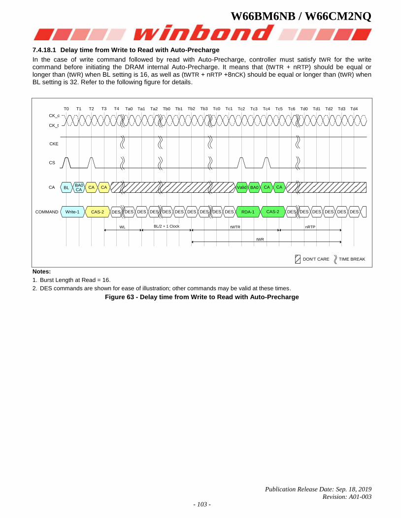
W66BM6NB / W66CM2NQ
Publication Release Date: Sep. 18, 2019
Revision: A01-003
- 103 -
7.4.18.1 Delay time from Write to Read with Auto-Precharge
In the case of write command followed by read with Auto-Precharge, controller must satisfy tWR for the write command before initiating the DRAM internal Auto-Precharge. It means that (tWTR + nRTP) should be equal or longer than (tWR) when BL setting is 16, as well as (tWTR + nRTP +8nCK) should be equal or longer than (tWR) when BL setting is 32. Refer to the following figure for details.
CK_c
CK_t
CKE
CS
CA
COMMAND
T0
tWR
WL
T1 T2 T3 Ta0 Ta1 Ta2 Tb0 Tb2 Tb3 Tc0 Tc1 Tc6 Td0 Td1 Td2 Td3 Td4Tc3 Tc4
BL CA CACABA0
Valid CA CABA0
Write-1 CAS-2 DES DES RDA-1 CAS-2
TIME BREAKDON'T CARE
T4 Tb1 Tc2 Tc5
DES DES DES DESDES DES DES DES
BL/2 + 1 Clock nRTP
DES DES DES DESDES DES
tWTR
Notes:
1. Burst Length at Read = 16.
2. DES commands are shown for ease of illustration; other commands may be valid at these times.
Figure 63 - Delay time from Write to Read with Auto-Precharge
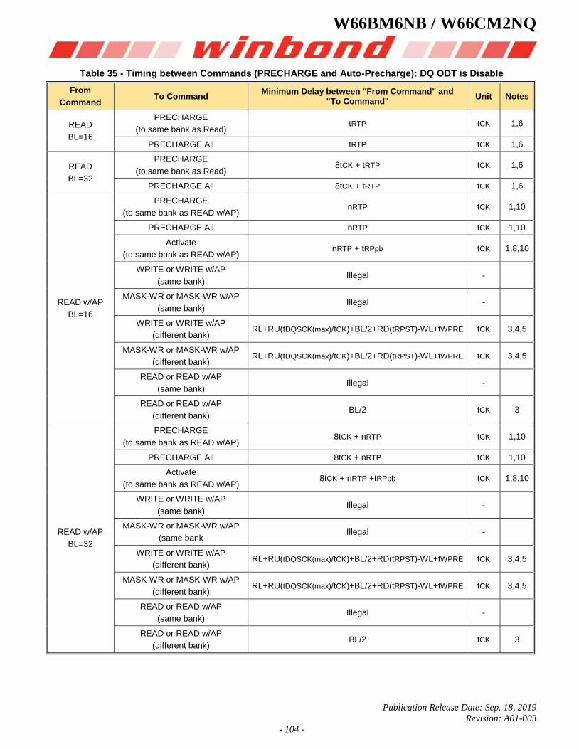
W66BM6NB / W66CM2NQ
Publication Release Date: Sep. 18, 2019
Revision: A01-003
- 104 -
Table 35 - Timing between Commands (PRECHARGE and Auto-Precharge): DQ ODT is Disable
From
Command To Command
Minimum Delay between "From Command" and "To Command"
Unit Notes
READ
BL=16
PRECHARGE
(to same bank as Read) tRTP tCK 1,6
PRECHARGE All tRTP tCK 1,6
READ
BL=32
PRECHARGE
(to same bank as Read) 8tCK + tRTP tCK 1,6
PRECHARGE All 8tCK + tRTP tCK 1,6
READ w/AP
BL=16
PRECHARGE
(to same bank as READ w/AP) nRTP tCK 1,10
PRECHARGE All nRTP tCK 1,10
Activate
(to same bank as READ w/AP) nRTP + tRPpb tCK 1,8,10
WRITE or WRITE w/AP
(same bank) Illegal -
MASK-WR or MASK-WR w/AP
(same bank) Illegal -
WRITE or WRITE w/AP
(different bank) RL+RU(tDQSCK(max)/tCK)+BL/2+RD(tRPST)-WL+tWPRE tCK 3,4,5
MASK-WR or MASK-WR w/AP
(different bank) RL+RU(tDQSCK(max)/tCK)+BL/2+RD(tRPST)-WL+tWPRE tCK 3,4,5
READ or READ w/AP
(same bank) Illegal -
READ or READ w/AP
(different bank) BL/2 tCK 3
READ w/AP
BL=32
PRECHARGE
(to same bank as READ w/AP) 8tCK + nRTP tCK 1,10
PRECHARGE All 8tCK + nRTP tCK 1,10
Activate
(to same bank as READ w/AP) 8tCK + nRTP +tRPpb tCK 1,8,10
WRITE or WRITE w/AP
(same bank) Illegal -
MASK-WR or MASK-WR w/AP
(same bank Illegal -
WRITE or WRITE w/AP
(different bank) RL+RU(tDQSCK(max)/tCK)+BL/2+RD(tRPST)-WL+tWPRE tCK 3,4,5
MASK-WR or MASK-WR w/AP
(different bank) RL+RU(tDQSCK(max)/tCK)+BL/2+RD(tRPST)-WL+tWPRE tCK 3,4,5
READ or READ w/AP
(same bank) Illegal -
READ or READ w/AP
(different bank) BL/2 tCK 3
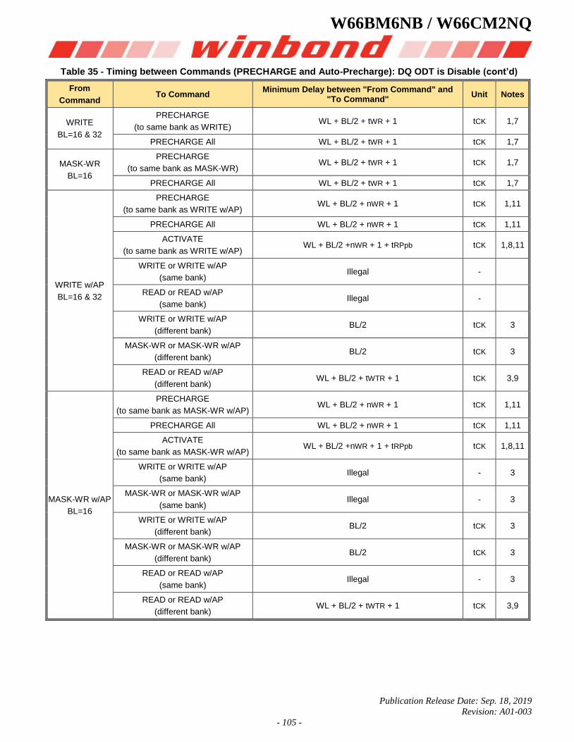
W66BM6NB / W66CM2NQ
Publication Release Date: Sep. 18, 2019
Revision: A01-003
- 105 -
Table 35 - Timing between Commands (PRECHARGE and Auto-Precharge): DQ ODT is Disable (cont’d)
From
Command To Command
Minimum Delay between "From Command" and "To Command"
Unit Notes
WRITE
BL=16 & 32
PRECHARGE
(to same bank as WRITE) WL + BL/2 + tWR + 1 tCK 1,7
PRECHARGE All WL + BL/2 + tWR + 1 tCK 1,7
MASK-WR
BL=16
PRECHARGE
(to same bank as MASK-WR) WL + BL/2 + tWR + 1 tCK 1,7
PRECHARGE All WL + BL/2 + tWR + 1 tCK 1,7
WRITE w/AP
BL=16 & 32
PRECHARGE
(to same bank as WRITE w/AP) WL + BL/2 + nWR + 1 tCK 1,11
PRECHARGE All WL + BL/2 + nWR + 1 tCK 1,11
ACTIVATE
(to same bank as WRITE w/AP) WL + BL/2 +nWR + 1 + tRPpb tCK 1,8,11
WRITE or WRITE w/AP
(same bank) Illegal -
READ or READ w/AP
(same bank) Illegal -
WRITE or WRITE w/AP
(different bank) BL/2 tCK 3
MASK-WR or MASK-WR w/AP
(different bank) BL/2 tCK 3
READ or READ w/AP
(different bank) WL + BL/2 + tWTR + 1 tCK 3,9
MASK-WR w/AP
BL=16
PRECHARGE
(to same bank as MASK-WR w/AP) WL + BL/2 + nWR + 1 tCK 1,11
PRECHARGE All WL + BL/2 + nWR + 1 tCK 1,11
ACTIVATE
(to same bank as MASK-WR w/AP) WL + BL/2 +nWR + 1 + tRPpb tCK 1,8,11
WRITE or WRITE w/AP
(same bank) Illegal - 3
MASK-WR or MASK-WR w/AP
(same bank) Illegal - 3
WRITE or WRITE w/AP
(different bank) BL/2 tCK 3
MASK-WR or MASK-WR w/AP
(different bank) BL/2 tCK 3
READ or READ w/AP
(same bank) Illegal - 3
READ or READ w/AP
(different bank) WL + BL/2 + tWTR + 1 tCK 3,9
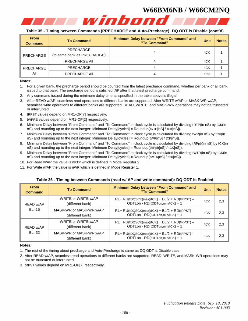
W66BM6NB / W66CM2NQ
Publication Release Date: Sep. 18, 2019
Revision: A01-003
- 106 -
Table 35 - Timing between Commands (PRECHARGE and Auto-Precharge): DQ ODT is Disable (cont’d)
From
Command To Command
Minimum Delay between "From Command" and "To Command"
Unit Notes
PRECHARGE
PRECHARGE
(to same bank as PRECHARGE) 4 tCK 1
PRECHARGE All 4 tCK 1
PRECHARGE
All
PRECHARGE 4 tCK 1
PRECHARGE All 4 tCK 1
Notes:
1. For a given bank, the precharge period should be counted from the latest precharge command, whether per bank or all bank, issued to that bank. The precharge period is satisfied tRP after that latest precharge command.
2. Any command issued during the minimum delay time as specified in the table above is illegal.
3. After READ w/AP, seamless read operations to different banks are supported. After WRITE w/AP or MASK-WR w/AP, seamless write operations to different banks are supported. READ, WRITE, and MASK-WR operations may not be truncated or interrupted.
4. tRPST values depend on MR1-OP[7] respectively.
5. tWPRE values depend on MR1-OP[2] respectively.
6. Minimum Delay between "From Command" and "To Command" in clock cycle is calculated by dividing tRTP(in nS) by tCK(in nS) and rounding up to the next integer: Minimum Delay[cycles] = Roundup(tRTP[nS] / tCK[nS]).
7. Minimum Delay between "From Command" and "To Command" in clock cycle is calculated by dividing tWR(in nS) by tCK(in nS) and rounding up to the next integer: Minimum Delay[cycles] = Roundup(tWR[nS] / tCK[nS]).
8. Minimum Delay between "From Command" and "To Command" in clock cycle is calculated by dividing tRPpb(in nS) by tCK(in nS) and rounding up to the next integer: Minimum Delay[cycles] = Roundup(tRPpb[nS] / tCK[nS]).
9. Minimum Delay between "From Command" and "To Command" in clock cycle is calculated by dividing tWTR(in nS) by tCK(in nS) and rounding up to the next integer: Minimum Delay[cycles] = Roundup(tWTR[nS] / tCK[nS]).
10. For Read w/AP the value is nRTP which is defined in Mode Register 2.
11. For Write w/AP the value is nWR which is defined in Mode Register 1.
Table 36 - Timing between Commands (read w/ AP and write command): DQ ODT is Enabled
From
Command To Command
Minimum Delay between "From Command" and "To Command"
Unit Notes
READ w/AP
BL=16
WRITE or WRITE w/AP
(different bank)
RL+ RU(tDQSCK(max)/tCK) + BL/2 + RD(tRPST) – ODTLon - RD(tODTon,min/tCK) + 1
tCK 2,3
MASK-WR or MASK-WR w/AP
(different bank)
RL+ RU(tDQSCK(max)/tCK) + BL/2 + RD(tRPST) – ODTLon - RD(tODTon,min/tCK) + 1
tCK 2,3
READ w/AP
BL=32
WRITE or WRITE w/AP
(different bank)
RL+ RU(tDQSCK(max)/tCK) + BL/2 + RD(tRPST) – ODTLon - RD(tODTon,min/tCK) + 1
tCK 2,3
MASK-WR or MASK-WR w/AP
(different bank)
RL+ RU(tDQSCK(max)/tCK) + BL/2 + RD(tRPST) – ODTLon - RD(tODTon,min/tCK) + 1
tCK 2,3
Notes:
1. The rest of the timing about precharge and Auto-Precharge is same as DQ ODT is Disable case.
2. After READ w/AP, seamless read operations to different banks are supported. READ, WRITE, and MASK-WR operations may not be truncated or interrupted.
3. tRPST values depend on MR1-OP[7] respectively.
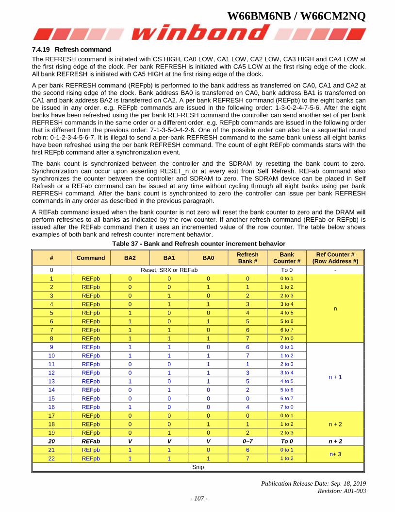
W66BM6NB / W66CM2NQ
Publication Release Date: Sep. 18, 2019
Revision: A01-003
- 107 -
7.4.19 Refresh command
The REFRESH command is initiated with CS HIGH, CA0 LOW, CA1 LOW, CA2 LOW, CA3 HIGH and CA4 LOW at the first rising edge of the clock. Per bank REFRESH is initiated with CA5 LOW at the first rising edge of the clock. All bank REFRESH is initiated with CA5 HIGH at the first rising edge of the clock.
A per bank REFRESH command (REFpb) is performed to the bank address as transferred on CA0, CA1 and CA2 at the second rising edge of the clock. Bank address BA0 is transferred on CA0, bank address BA1 is transferred on CA1 and bank address BA2 is transferred on CA2. A per bank REFRESH command (REFpb) to the eight banks can be issued in any order. e.g. REFpb commands are issued in the following order: 1-3-0-2-4-7-5-6. After the eight banks have been refreshed using the per bank REFRESH command the controller can send another set of per bank REFRESH commands in the same order or a different order. e.g. REFpb commands are issued in the following order that is different from the previous order: 7-1-3-5-0-4-2-6. One of the possible order can also be a sequential round robin: 0-1-2-3-4-5-6-7. It is illegal to send a per-bank REFRESH command to the same bank unless all eight banks have been refreshed using the per bank REFRESH command. The count of eight REFpb commands starts with the first REFpb command after a synchronization event.
The bank count is synchronized between the controller and the SDRAM by resetting the bank count to zero. Synchronization can occur upon asserting RESET_n or at every exit from Self Refresh. REFab command also synchronizes the counter between the controller and SDRAM to zero. The SDRAM device can be placed in Self Refresh or a REFab command can be issued at any time without cycling through all eight banks using per bank REFRESH command. After the bank count is synchronized to zero the controller can issue per bank REFRESH commands in any order as described in the previous paragraph.
A REFab command issued when the bank counter is not zero will reset the bank counter to zero and the DRAM will perform refreshes to all banks as indicated by the row counter. If another refresh command (REFab or REFpb) is issued after the REFab command then it uses an incremented value of the row counter. The table below shows examples of both bank and refresh counter increment behavior.
Table 37 - Bank and Refresh counter increment behavior
# Command BA2 BA1 BA0 Refresh Bank #
Bank Counter #
Ref Counter # (Row Address #)
0 Reset, SRX or REFab To 0 -
1 REFpb 0 0 0 0 0 to 1
n
2 REFpb 0 0 1 1 1 to 2
3 REFpb 0 1 0 2 2 to 3
4 REFpb 0 1 1 3 3 to 4
5 REFpb 1 0 0 4 4 to 5
6 REFpb 1 0 1 5 5 to 6
7 REFpb 1 1 0 6 6 to 7
8 REFpb 1 1 1 7 7 to 0
9 REFpb 1 1 0 6 0 to 1
n + 1
10 REFpb 1 1 1 7 1 to 2
11 REFpb 0 0 1 1 2 to 3
12 REFpb 0 1 1 3 3 to 4
13 REFpb 1 0 1 5 4 to 5
14 REFpb 0 1 0 2 5 to 6
15 REFpb 0 0 0 0 6 to 7
16 REFpb 1 0 0 4 7 to 0
17 REFpb 0 0 0 0 0 to 1
n + 2 18 REFpb 0 0 1 1 1 to 2
19 REFpb 0 1 0 2 2 to 3
20 REFab V V V 0~7 To 0 n + 2
21 REFpb 1 1 0 6 0 to 1 n+ 3
22 REFpb 1 1 1 7 1 to 2
Snip
W66BM6NB / W66CM2NQ
Publication Release Date: Sep. 18, 2019
Revision: A01-003
- 108 -
A bank must be idle before it can be refreshed. The controller must track the bank being refreshed by the per bank REFRESH command.
The REFpb command must not be issued to the device until the following conditions are met:
- tRFCab has been satisfied after the prior REFab command.
- tRFCpb has been satisfied after the prior REFpb command.
- tRP has been satisfied after the prior PRECHARGE command to the same bank.
- tpbR2pbR has been satisfied after the prior REFpb command to different bank.
- tRRD has been satisfied after the prior ACTIVATE command (if applicable, for example after activating a row in a different bank than the one affected by the REFpb command).
The target bank is inaccessible during per bank REFRESH cycle time (tRFCpb) or Per-bank Refresh to Per-bank Refresh different bank Time (tpbR2pbR), however, other banks within the device are accessible and can be addressed during the cycle. During the REFpb operation, any of the banks other than the one being refreshed can be maintained in an active state or accessed by a READ or a WRITE command. When the per-bank REFRESH cycle has completed, the affected bank will be in the idle state.
After issuing REFpb, these conditions must be met:
- tRFCpb must be satisfied before issuing a REFab command.
- tRFCpb must be satisfied before issuing an ACTIVATE command to the same bank.
- tRRD must be satisfied before issuing an ACTIVATE command to a different bank.
- tRFCpb must be satisfied before issuing another REFpb command to the same bank.
- tpbR2pbR must be satisfied before issuing another REFpb command to a different bank.
An all bank REFRESH command (REFab) issues a REFRESH command to all banks. All banks must be idle when REFab is issued (for instance, by issuing a PRECHARGE-all command prior to issuing an all bank REFRESH command). REFab also synchronizes the bank count between the controller and the SDRAM to zero. The REFab command must not be issued to the device until the following conditions have been met:
- tRFCab has been satisfied following the prior REFab command.
- tRFCpb has been satisfied following the prior REFpb command.
- tRP has been satisfied following the prior PRECHARGE commands.
When an all bank refresh cycle has completed, all banks will be idle. After issuing REFab:
- tRFCab latency must be satisfied before issuing an ACTIVATE command.
- tRFCab latency must be satisfied before issuing a REFab or REFpb command.
Table 38 - REFRESH Command Scheduling Separation requirements
Symbol Minimum Delay
From To Notes
tRFCab REFab
REFab
Activate command to any bank
REFpb
tRFCpb REFpb
REFab
Activate command to same bank as REFpb
REFpb to the same bank
tpbR2pbR REFpb REFpb to a different bank
tRRD
REFpb Activate command to different bank than REFpb
Activate REFpb 1
Activate command to different bank than prior Activate command
Note:
1. A bank must be in the idle state before it is refreshed, so following an ACTIVATE command REFab is prohibited; REFpb is supported only if it affects a bank that is in the idle state.
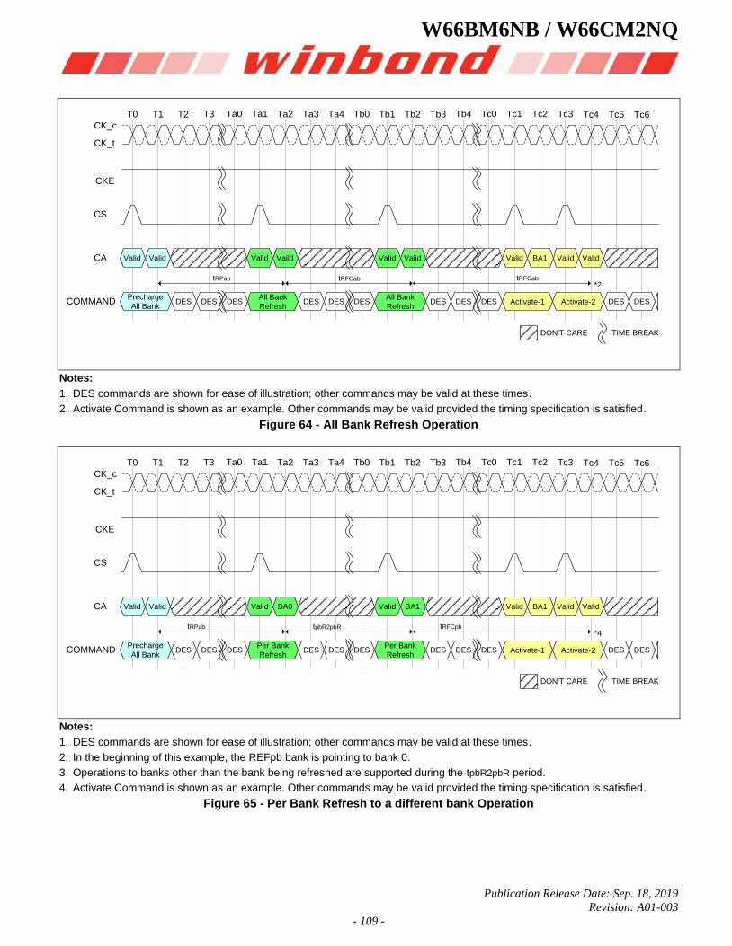
W66BM6NB / W66CM2NQ
Publication Release Date: Sep. 18, 2019
Revision: A01-003
- 109 -
Valid Valid Valid Valid Valid Valid Valid BA1 Valid Valid
DES DES DES DES DES DES DES DES DES DESPrecharge
All Bank
All Bank
Refresh
All Bank
RefreshActivate-1 Activate-2DES
T0 T1 T2 T3 Ta0 Ta1 Ta2 Ta3 Ta4 Tb0 Tb1 Tb2 Tb3 Tb4 Tc0 Tc1 Tc2 Tc3 Tc4 Tc5 Tc6CK_c
CK_t
COMMAND
CA
CS
CKE
TIME BREAKDON'T CARE
tRFCabtRPab tRFCab*2
Notes:
1. DES commands are shown for ease of illustration; other commands may be valid at these times.
2. Activate Command is shown as an example. Other commands may be valid provided the timing specification is satisfied.
Figure 64 - All Bank Refresh Operation
Valid Valid Valid BA0 Valid BA1 Valid BA1 Valid Valid
DES DES DES DES DES DES DES DES DES DESPrecharge
All Bank
Per Bank
Refresh
Per Bank
RefreshActivate-1 Activate-2DES
T0 T1 T2 T3 Ta0 Ta1 Ta2 Ta3 Ta4 Tb0 Tb1 Tb2 Tb3 Tb4 Tc0 Tc1 Tc2 Tc3 Tc4 Tc5 Tc6CK_c
CK_t
COMMAND
CA
CS
CKE
TIME BREAKDON'T CARE
tpbR2pbRtRPab tRFCpb*4
Notes:
1. DES commands are shown for ease of illustration; other commands may be valid at these times.
2. In the beginning of this example, the REFpb bank is pointing to bank 0.
3. Operations to banks other than the bank being refreshed are supported during the tpbR2pbR period.
4. Activate Command is shown as an example. Other commands may be valid provided the timing specification is satisfied.
Figure 65 - Per Bank Refresh to a different bank Operation
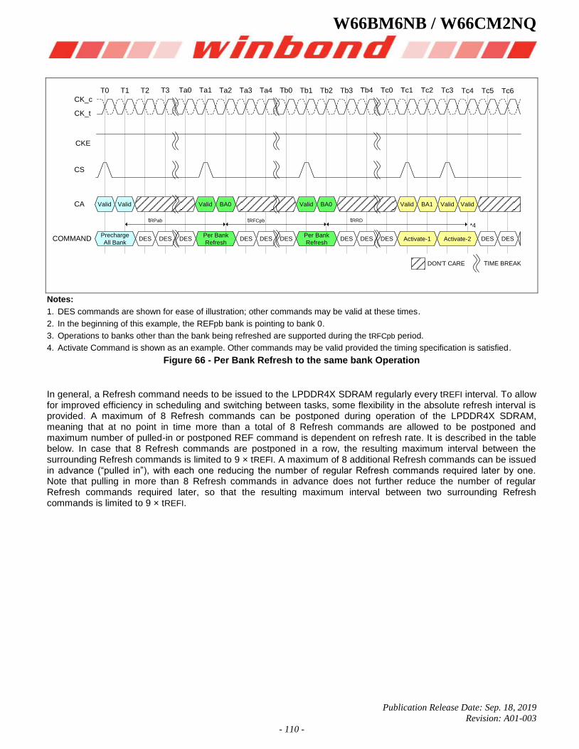
W66BM6NB / W66CM2NQ
Publication Release Date: Sep. 18, 2019
Revision: A01-003
- 110 -
Valid Valid Valid BA0 Valid BA0 Valid BA1 Valid Valid
DES DES DES DES DES DES DES DES DES DESPrecharge
All Bank
Per Bank
Refresh
Per Bank
RefreshActivate-1 Activate-2DES
T0 T1 T2 T3 Ta0 Ta1 Ta2 Ta3 Ta4 Tb0 Tb1 Tb2 Tb3 Tb4 Tc0 Tc1 Tc2 Tc3 Tc4 Tc5 Tc6CK_c
CK_t
COMMAND
CA
CS
CKE
TIME BREAKDON'T CARE
tRFCpbtRPab tRRD*4
Notes:
1. DES commands are shown for ease of illustration; other commands may be valid at these times.
2. In the beginning of this example, the REFpb bank is pointing to bank 0.
3. Operations to banks other than the bank being refreshed are supported during the tRFCpb period.
4. Activate Command is shown as an example. Other commands may be valid provided the timing specification is satisfied.
Figure 66 - Per Bank Refresh to the same bank Operation
In general, a Refresh command needs to be issued to the LPDDR4X SDRAM regularly every tREFI interval. To allow for improved efficiency in scheduling and switching between tasks, some flexibility in the absolute refresh interval is provided. A maximum of 8 Refresh commands can be postponed during operation of the LPDDR4X SDRAM, meaning that at no point in time more than a total of 8 Refresh commands are allowed to be postponed and maximum number of pulled-in or postponed REF command is dependent on refresh rate. It is described in the table below. In case that 8 Refresh commands are postponed in a row, the resulting maximum interval between the surrounding Refresh commands is limited to 9 × tREFI. A maximum of 8 additional Refresh commands can be issued in advance (“pulled in”), with each one reducing the number of regular Refresh commands required later by one. Note that pulling in more than 8 Refresh commands in advance does not further reduce the number of regular Refresh commands required later, so that the resulting maximum interval between two surrounding Refresh commands is limited to 9 × tREFI.
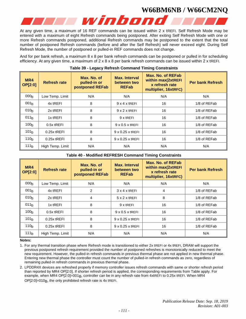
W66BM6NB / W66CM2NQ
Publication Release Date: Sep. 18, 2019
Revision: A01-003
- 111 -
At any given time, a maximum of 16 REF commands can be issued within 2 x tREFI. Self Refresh Mode may be entered with a maximum of eight Refresh commands being postponed. After exiting Self Refresh Mode with one or more Refresh commands postponed, additional Refresh commands may be postponed to the extent that the total number of postponed Refresh commands (before and after the Self Refresh) will never exceed eight. During Self Refresh Mode, the number of postponed or pulled-in REF commands does not change.
And for per bank refresh, a maximum 8 x 8 per bank refresh commands can be postponed or pulled in for scheduling efficiency. At any given time, a maximum of 2 x 8 x 8 per bank refresh commands can be issued within 2 x tREFI.
Table 39 - Legacy Refresh Command Timing Constraints
MR4 OP[2:0]
Refresh rate Max. No. of pulled-in or
postponed REFab
Max. Interval between two
REFab
Max. No. of REFab within max(2xtREFI
x refresh rate multiplier, 16xtRFC)
Per bank Refresh
000b Low Temp. Limit N/A N/A N/A N/A
001b 4x tREFI 8 9 x 4 x tREFI 16 1/8 of REFab
010b 2x tREFI 8 9 x 2 x tREFI 16 1/8 of REFab
011b 1x tREFI 8 9 x tREFI 16 1/8 of REFab
100b 0.5x tREFI 8 9 x 0.5 x tREFI 16 1/8 of REFab
101b 0.25x tREFI 8 9 x 0.25 x tREFI 16 1/8 of REFab
110b 0.25x tREFI 8 9 x 0.25 x tREFI 16 1/8 of REFab
111b High Temp. Limit N/A N/A N/A N/A
Table 40 - Modified REFRESH Command Timing Constraints
MR4 OP[2:0]
Refresh rate Max. No. of pulled-in or
postponed REFab
Max. Interval between two
REFab
Max. No. of REFab within max(2xtREFI
x refresh rate multiplier, 16xtRFC)
Per bank Refresh
000b Low Temp. Limit N/A N/A N/A N/A
001b 4x tREFI 2 3 x 4 x tREFI 4 1/8 of REFab
010b 2x tREFI 4 5 x 2 x tREFI 8 1/8 of REFab
011b 1x tREFI 8 9 x tREFI 16 1/8 of REFab
100b 0.5x tREFI 8 9 x 0.5 x tREFI 16 1/8 of REFab
101b 0.25x tREFI 8 9 x 0.25 x tREFI 16 1/8 of REFab
110b 0.25x tREFI 8 9 x 0.25 x tREFI 16 1/8 of REFab
111b High Temp. Limit N/A N/A N/A N/A
Notes:
1. For any thermal transition phase where Refresh mode is transitioned to either 2x tREFI or 4x tREFI, DRAM will support the previous postponed refresh requirement provided the number of postponed refreshes is monotonically reduced to meet the new requirement. However, the pulled-in refresh commands in previous thermal phase are not applied in new thermal phase. Entering new thermal phase the controller must count the number of pulled-in refresh commands as zero, regardless of remaining pulled-in refresh commands in previous thermal phase.
2. LPDDR4X devices are refreshed properly if memory controller issues refresh commands with same or shorter refresh period than reported by MR4 OP[2:0]. If shorter refresh period is applied, the corresponding requirements from Table apply. For example, when MR4 OP[2:0]=001B, controller can be in any refresh rate from 4xtREFI to 0.25x tREFI. When MR4
OP[2:0]=010B, the only prohibited refresh rate is 4x tREFI.
W66BM6NB / W66CM2NQ
Publication Release Date: Sep. 18, 2019
Revision: A01-003
- 112 -
8 REF-Commands postponed
tREFI
9 x tREFI
t
tRFC
Figure 67 - Postponing Refresh Commands (Example)
8 REF-Commands pulled-in
tREFI
9 x tREFI
t
tRFC
Figure 68 - Pulling-in Refresh Commands (Example)
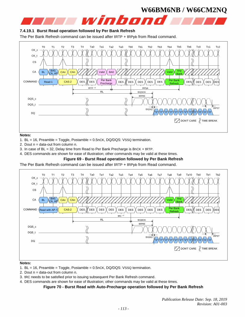
W66BM6NB / W66CM2NQ
Publication Release Date: Sep. 18, 2019
Revision: A01-003
- 113 -
7.4.19.1 Burst Read operation followed by Per Bank Refresh
The Per Bank Refresh command can be issued after tRTP + tRPpb from Read command.
TIME BREAK
CK_c
CK_t
COMMAND
DQS_c
DQS_t
DQ
T0 T1 T2 T3 T4 Ta0 Ta1 Ta2 Ta3 Tb0 Tb1 Tb2 Tb3 Tb4 Tb5 Tb6 Tc0 Tc1 Tc2
RL
tRTP *3
tRPRE
tRPSTtDQSQ
Dout n0
Dout n1
Dout n2
Dout n3
Dout n4
Dout n5
Dout n6
Dout n7
Dout n12
Dout n13
Dout n14
Dout n15
tDQSCK
BL CAnCAnCA
CS
Read-1 CAS-2 DES DESDES DES DES DES DES DES DES DES DES
BA0,CA, AP
ValidAny
Bank
Per Bank
Refresh
DON'T CARE
Valid
Per Bank
Precharge
BA0
tRPpb
Notes:
1. BL = 16, Preamble = Toggle, Postamble = 0.5nCK, DQ/DQS: VSSQ termination.
2. Dout n = data-out from column n.
3. In case of BL = 32, Delay time from Read to Per Bank Precharge is 8nCK + tRTP.
4. DES commands are shown for ease of illustration; other commands may be valid at these times.
Figure 69 - Burst Read operation followed by Per Bank Refresh
The Per Bank Refresh command can be issued after tRTP + tRPpb from Read command.
TIME BREAK
CK_c
CK_t
COMMAND
DQS_c
DQS_t
DQ
T0 T1 T2 T3 T4 Ta0 Ta1 Ta2 Ta3 Ta4 Ta5 Ta6 Ta7 Ta8 Ta9 Ta10 Tb0 Tb1 Tb2
RL
tRC *3
tRPRE
tRPSTtDQSQ
Dout n0
Dout n1
Dout n2
Dout n3
Dout n4
Dout n5
Dout n6
Dout n7
Dout n12
Dout n13
Dout n14
Dout n15
tDQSCK
BL CAnCAnCA
CS
Read with AP-1 CAS-2 DES DESDES DES DES DES DES DES DES DES DES DES DES
BA0,CA, AP
ValidAny
Bank
Per Bank
Refresh
DON'T CARE
Notes:
1. BL = 16, Preamble = Toggle, Postamble = 0.5nCK, DQ/DQS: VSSQ termination.
2. Dout n = data-out from column n.
3. tRC needs to be satisfied prior to issuing subsequent Per Bank Refresh command.
4. DES commands are shown for ease of illustration; other commands may be valid at these times.
Figure 70 - Burst Read with Auto-Precharge operation followed by Per Bank Refresh
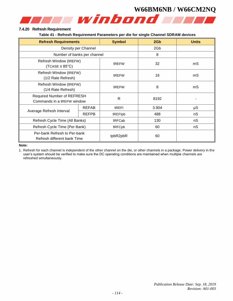
W66BM6NB / W66CM2NQ
Publication Release Date: Sep. 18, 2019
Revision: A01-003
- 114 -
7.4.20 Refresh Requirement
Table 41 - Refresh Requirement Parameters per die for single Channel SDRAM devices
Refresh Requirements Symbol 2Gb Units
Density per Channel 2Gb
Number of banks per channel 8
Refresh Window (tREFW)
(TCASE ≤ 85°C) tREFW 32 mS
Refresh Window (tREFW)
(1/2 Rate Refresh) tREFW 16 mS
Refresh Window (tREFW)
(1/4 Rate Refresh) tREFW 8 mS
Required Number of REFRESH
Commands in a tREFW window R 8192 -
Average Refresh Interval REFAB tREFI 3.904 µS
REFPB tREFIpb 488 nS
Refresh Cycle Time (All Banks) tRFCab 130 nS
Refresh Cycle Time (Per Bank) tRFCpb 60 nS
Per-bank Refresh to Per-bank
Refresh different bank Time tpbR2pbR 60
Note:
1. Refresh for each channel is independent of the other channel on the die, or other channels in a package. Power delivery in the user’s system should be verified to make sure the DC operating conditions are maintained when multiple channels are refreshed simultaneously.
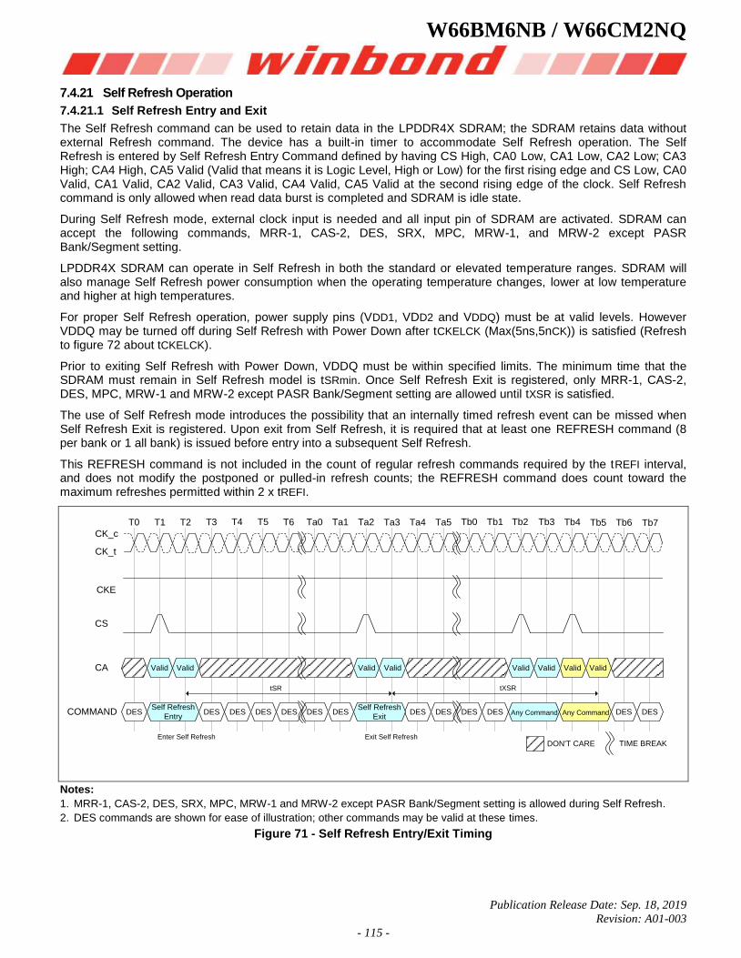
W66BM6NB / W66CM2NQ
Publication Release Date: Sep. 18, 2019
Revision: A01-003
- 115 -
7.4.21 Self Refresh Operation
7.4.21.1 Self Refresh Entry and Exit
The Self Refresh command can be used to retain data in the LPDDR4X SDRAM; the SDRAM retains data without external Refresh command. The device has a built-in timer to accommodate Self Refresh operation. The Self Refresh is entered by Self Refresh Entry Command defined by having CS High, CA0 Low, CA1 Low, CA2 Low; CA3 High; CA4 High, CA5 Valid (Valid that means it is Logic Level, High or Low) for the first rising edge and CS Low, CA0 Valid, CA1 Valid, CA2 Valid, CA3 Valid, CA4 Valid, CA5 Valid at the second rising edge of the clock. Self Refresh command is only allowed when read data burst is completed and SDRAM is idle state.
During Self Refresh mode, external clock input is needed and all input pin of SDRAM are activated. SDRAM can accept the following commands, MRR-1, CAS-2, DES, SRX, MPC, MRW-1, and MRW-2 except PASR Bank/Segment setting.
LPDDR4X SDRAM can operate in Self Refresh in both the standard or elevated temperature ranges. SDRAM will also manage Self Refresh power consumption when the operating temperature changes, lower at low temperature and higher at high temperatures.
For proper Self Refresh operation, power supply pins (VDD1, VDD2 and VDDQ) must be at valid levels. However VDDQ may be turned off during Self Refresh with Power Down after tCKELCK (Max(5ns,5nCK)) is satisfied (Refresh to figure 72 about tCKELCK).
Prior to exiting Self Refresh with Power Down, VDDQ must be within specified limits. The minimum time that the SDRAM must remain in Self Refresh model is tSRmin. Once Self Refresh Exit is registered, only MRR-1, CAS-2, DES, MPC, MRW-1 and MRW-2 except PASR Bank/Segment setting are allowed until tXSR is satisfied.
The use of Self Refresh mode introduces the possibility that an internally timed refresh event can be missed when Self Refresh Exit is registered. Upon exit from Self Refresh, it is required that at least one REFRESH command (8 per bank or 1 all bank) is issued before entry into a subsequent Self Refresh.
This REFRESH command is not included in the count of regular refresh commands required by the tREFI interval, and does not modify the postponed or pulled-in refresh counts; the REFRESH command does count toward the maximum refreshes permitted within 2 x tREFI.
Valid Valid Valid Valid Valid Valid Valid Valid
DES DES DES DES DES DES DES DES DES DESSelf Refresh
Entry
Self Refresh
ExitAny CommandDES
T0 T1 T2 T3 T4 T5 T6 Ta0 Ta1 Ta2 Ta3 Ta4 Ta5 Tb0 Tb1 Tb2 Tb3 Tb4 Tb5 Tb6 Tb7CK_c
CK_t
COMMAND
CA
CS
CKE
TIME BREAKDON'T CARE
tSR tXSR
DES Any CommandDES
Enter Self Refresh Exit Self Refresh
Notes:
1. MRR-1, CAS-2, DES, SRX, MPC, MRW-1 and MRW-2 except PASR Bank/Segment setting is allowed during Self Refresh.
2. DES commands are shown for ease of illustration; other commands may be valid at these times.
Figure 71 - Self Refresh Entry/Exit Timing

W66BM6NB / W66CM2NQ
Publication Release Date: Sep. 18, 2019
Revision: A01-003
- 116 -
7.4.21.2 Power Down Entry and Exit during Self Refresh
Entering/Exiting Power Down Mode is allowed during Self Refresh mode in SDRAM. The related timing parameters between Self Refresh Entry/Exit and Power Down Entry/Exit are shown in Figure 72.
Valid Valid Valid Valid Valid
DES DESSelf Refresh
Entry
Self Refresh
ExitAny Command
T0 T1 T2 T3 Ta0 Tb0 Tb1 Tc0 Td1 Te0 Tf0 Tf1 Tg0 Tg1 Th0 Tk0 Tk1 Tk2 Tk3CK_c
CK_t
COMMAND
CA
CS
CKE
tSR
DES DES
Enter Self Refresh Exit Self Refresh
Valid
*3
TIME BREAKDON'T CARE
tCMDCKE
tESCKE
tCSCKEH tCKEHCStCSCKE tCKELCS
tCKELCK tCKCKEH
tCKE
*2
tXP
Notes:
1. MRR-1, CAS-2, DES, SRX, MPC, MRW-1 and MRW-2 except PASR Bank/Segment setting is allowed during Self Refresh.
2. Input clock frequency can be changed or the input clock can be stopped or floated after tCKELCK satisfied and during power-down, provided that upon exiting power-down, the clock is stable and within specified limits for a minimum of tCKCKEH of stable clock prior to power-down exit and the clock frequency is between the minimum and maximum specified frequency for the speed grade in use.
3. 2 Clock command for example.
Figure 72 - Self Refresh Entry/Exit Timing with Power Down Entry/Exit
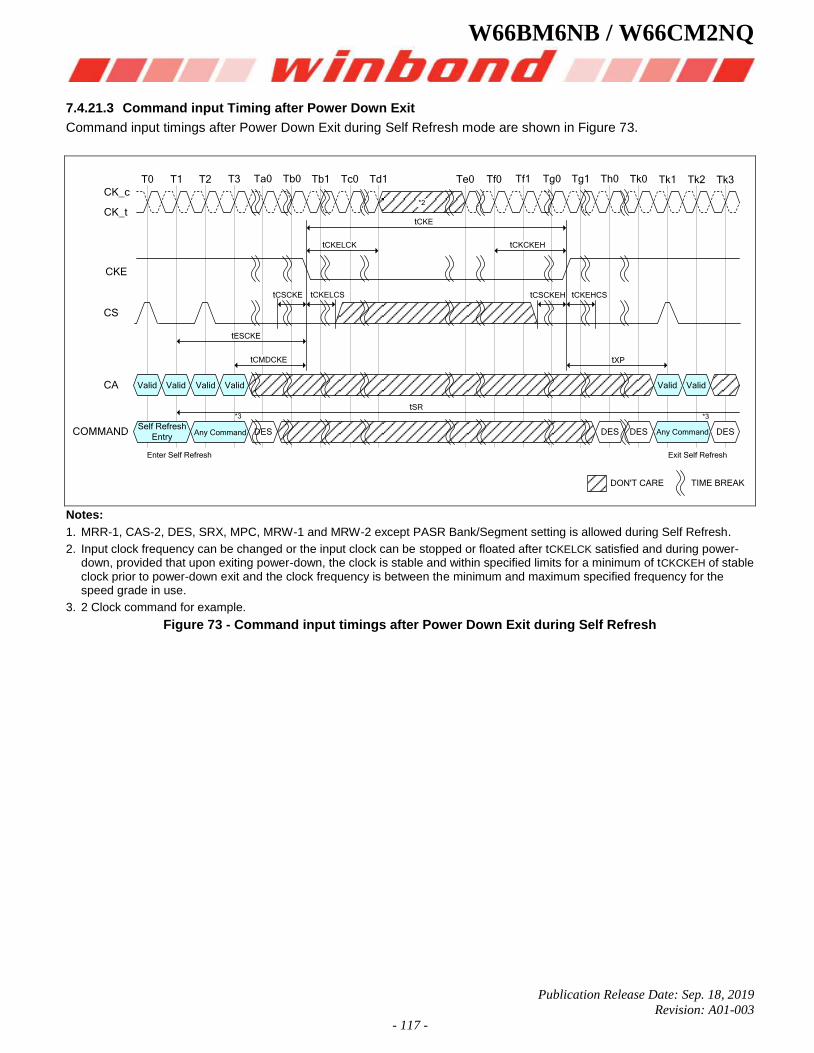
W66BM6NB / W66CM2NQ
Publication Release Date: Sep. 18, 2019
Revision: A01-003
- 117 -
7.4.21.3 Command input Timing after Power Down Exit
Command input timings after Power Down Exit during Self Refresh mode are shown in Figure 73.
Valid Valid Valid Valid Valid
DES DESSelf Refresh
EntryAny Command
T0 T1 T2 T3 Ta0 Tb0 Tb1 Tc0 Td1 Te0 Tf0 Tf1 Tg0 Tg1 Th0 Tk0 Tk1 Tk2 Tk3CK_c
CK_t
COMMAND
CA
CS
CKE
tSR
DES DES
Enter Self Refresh Exit Self Refresh
Valid
*3
TIME BREAKDON'T CARE
tCMDCKE
tESCKE
tCSCKEH tCKEHCStCSCKE tCKELCS
tCKELCK tCKCKEH
tCKE
*2
tXP
*3
Any Command
Notes:
1. MRR-1, CAS-2, DES, SRX, MPC, MRW-1 and MRW-2 except PASR Bank/Segment setting is allowed during Self Refresh.
2. Input clock frequency can be changed or the input clock can be stopped or floated after tCKELCK satisfied and during power-down, provided that upon exiting power-down, the clock is stable and within specified limits for a minimum of tCKCKEH of stable clock prior to power-down exit and the clock frequency is between the minimum and maximum specified frequency for the speed grade in use.
3. 2 Clock command for example.
Figure 73 - Command input timings after Power Down Exit during Self Refresh
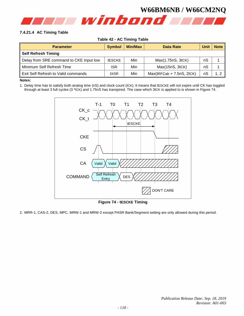
W66BM6NB / W66CM2NQ
Publication Release Date: Sep. 18, 2019
Revision: A01-003
- 118 -
7.4.21.4 AC Timing Table
Table 42 - AC Timing Table
Parameter Symbol Min/Max Data Rate Unit Note
Self Refresh Timing
Delay from SRE command to CKE Input low tESCKE Min Max(1.75nS, 3tCK) nS 1
Minimum Self Refresh Time tSR Min Max(15nS, 3tCK) nS 1
Exit Self Refresh to Valid commands tXSR Min Max(tRFCab + 7.5nS, 2tCK) nS 1, 2
Notes:
1. Delay time has to satisfy both analog time (nS) and clock count (tCK). It means that tESCKE will not expire until CK has toggled through at least 3 full cycles (3 *tCK) and 1.75nS has transpired. The case which 3tCK is applied to is shown in Figure 74.
T-1 T4
DON'T CARE
COMMAND
T3
T2T1T0
CA
CS
CKE
CK_t
CK_c
tESCKE
Valid Valid
Self Refresh
EntryDES
Figure 74 - tESCKE Timing
2. MRR-1, CAS-2, DES, MPC, MRW-1 and MRW-2 except PASR Bank/Segment setting are only allowed during this period.
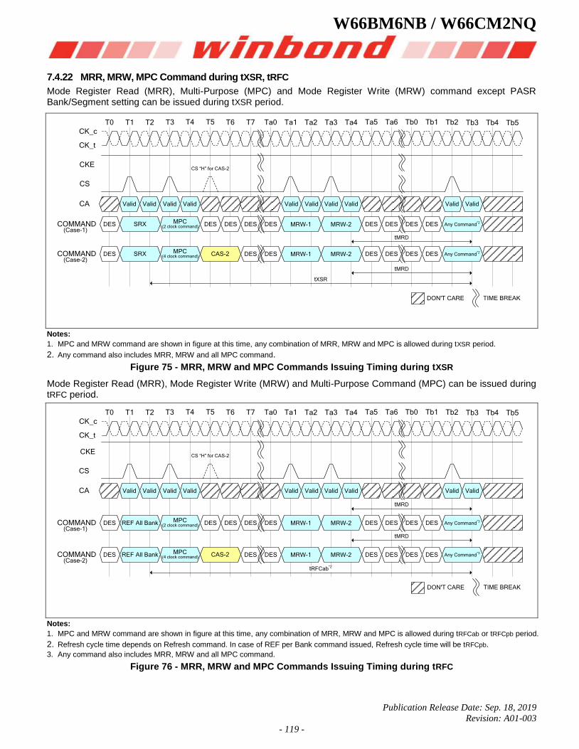
W66BM6NB / W66CM2NQ
Publication Release Date: Sep. 18, 2019
Revision: A01-003
- 119 -
7.4.22 MRR, MRW, MPC Command during tXSR, tRFC
Mode Register Read (MRR), Multi-Purpose (MPC) and Mode Register Write (MRW) command except PASR Bank/Segment setting can be issued during tXSR period.
Valid Valid Valid Valid Valid Valid Valid Valid
DES DES DES DES DES DESSRX DES
T0 T1 T2 T3 T4 T5 T6 T7 Ta0 Ta1 Ta2 Ta3 Ta4 Ta5 Ta6 Tb0 Tb1 Tb2 Tb3 Tb4 Tb5CK_c
CK_t
COMMAND
CA
CS
CKE
tXSR
tMRD
DES Any Command*2DES
Valid Valid
TIME BREAKDON'T CARE
(Case-1)(2 clock command)
MPC MRW-1 MRW-2
DES DES DES DES DESSRX DESCOMMAND
tMRD
Any Command*2DES
(Case-2)(4 clock command)
MPC MRW-1 MRW-2CAS-2
CS “H” for CAS-2
Notes:
1. MPC and MRW command are shown in figure at this time, any combination of MRR, MRW and MPC is allowed during tXSR period.
2. Any command also includes MRR, MRW and all MPC command.
Figure 75 - MRR, MRW and MPC Commands Issuing Timing during tXSR
Mode Register Read (MRR), Mode Register Write (MRW) and Multi-Purpose Command (MPC) can be issued during tRFC period.
Valid Valid Valid Valid Valid Valid Valid Valid
DES DES DES DES DES DESREF All Bank DES
T0 T1 T2 T3 T4 T5 T6 T7 Ta0 Ta1 Ta2 Ta3 Ta4 Ta5 Ta6 Tb0 Tb1 Tb2 Tb3 Tb4 Tb5CK_c
CK_t
COMMAND
CA
CS
CKE
tRFCab*2
tMRD
DES Any Command*3DES
Valid Valid
TIME BREAKDON'T CARE
(Case-1)(2 clock command)
MPC MRW-1 MRW-2
DES DES DES DES DESDESCOMMAND
tMRD
Any Command*3DES
(Case-2)(4 clock command)
MPC MRW-1 MRW-2CAS-2
CS “H” for CAS-2
REF All Bank
Notes:
1. MPC and MRW command are shown in figure at this time, any combination of MRR, MRW and MPC is allowed during tRFCab or tRFCpb period.
2. Refresh cycle time depends on Refresh command. In case of REF per Bank command issued, Refresh cycle time will be tRFCpb. 3. Any command also includes MRR, MRW and all MPC command.
Figure 76 - MRR, MRW and MPC Commands Issuing Timing during tRFC
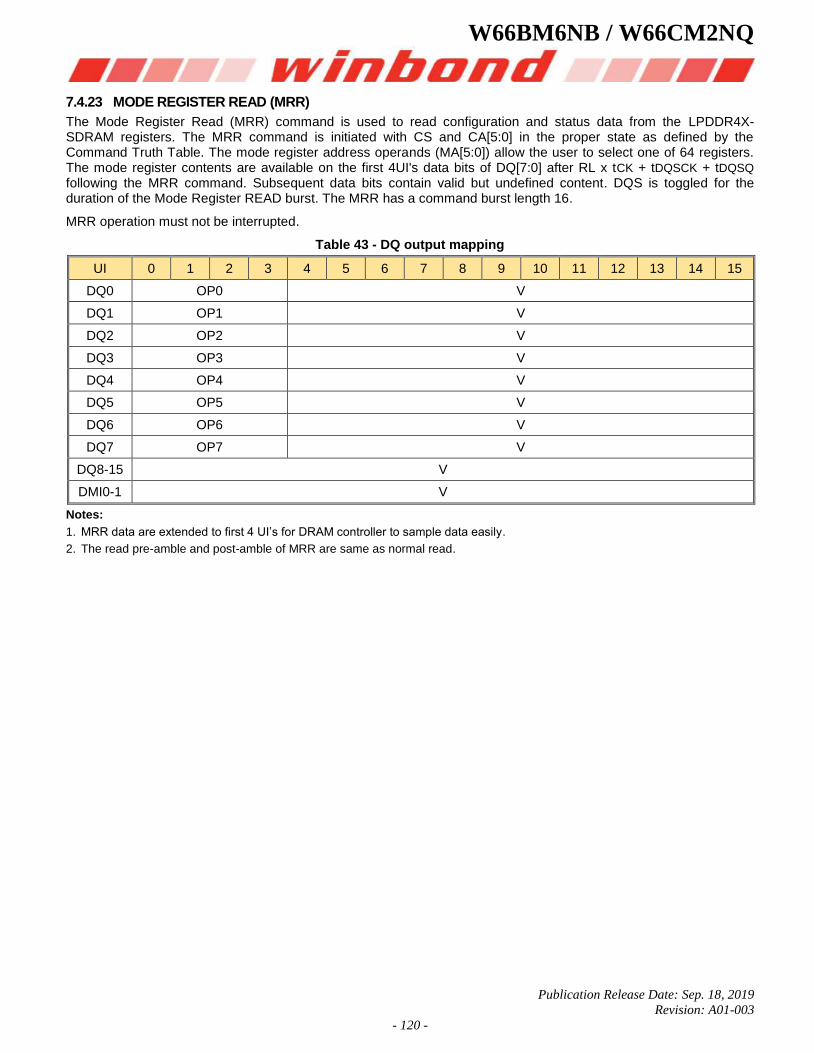
W66BM6NB / W66CM2NQ
Publication Release Date: Sep. 18, 2019
Revision: A01-003
- 120 -
7.4.23 MODE REGISTER READ (MRR)
The Mode Register Read (MRR) command is used to read configuration and status data from the LPDDR4X-SDRAM registers. The MRR command is initiated with CS and CA[5:0] in the proper state as defined by the Command Truth Table. The mode register address operands (MA[5:0]) allow the user to select one of 64 registers. The mode register contents are available on the first 4UI's data bits of DQ[7:0] after RL x tCK + tDQSCK + tDQSQ following the MRR command. Subsequent data bits contain valid but undefined content. DQS is toggled for the duration of the Mode Register READ burst. The MRR has a command burst length 16.
MRR operation must not be interrupted.
Table 43 - DQ output mapping
UI 0 1 2 3 4 5 6 7 8 9 10 11 12 13 14 15
DQ0 OP0 V
DQ1 OP1 V
DQ2 OP2 V
DQ3 OP3 V
DQ4 OP4 V
DQ5 OP5 V
DQ6 OP6 V
DQ7 OP7 V
DQ8-15 V
DMI0-1 V
Notes:
1. MRR data are extended to first 4 UI’s for DRAM controller to sample data easily.
2. The read pre-amble and post-amble of MRR are same as normal read.
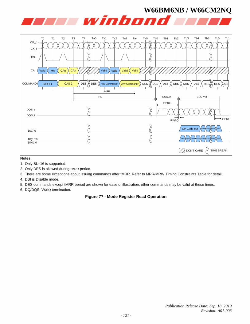
W66BM6NB / W66CM2NQ
Publication Release Date: Sep. 18, 2019
Revision: A01-003
- 121 -
CK_c
CK_t
T0 T1 T2 T3 T4 Ta0 Ta1 Ta2 Ta3 Ta4 Ta5 Tb0 Tb1 Tb2 Tb3 Tb4 Tb5 Tc0 Tc1
MRR-1 CAS-2
Valid MA CAnCAn
tRPST
tRPRE
RL
DES DESDES DES DES DES DES DES DES DES DESCOMMAND
CS
CA
DON'T CARE TIME BREAK
Valid Valid ValidValid
Any Command3 Any Command3
tMRR
tDQSCK BL/2 = 8
tDQSQ
Valid ValidValid ValidValid ValidValidValid
Valid ValidValidValidOP Code out
DQS_c
DQS_t
DQ15:8
DMI1:0
DQ7:0
Notes:
1. Only BL=16 is supported.
2. Only DES is allowed during tMRR period.
3. There are some exceptions about issuing commands after tMRR. Refer to MRR/MRW Timing Constraints Table for detail.
4. DBI is Disable mode.
5. DES commands except tMRR period are shown for ease of illustration; other commands may be valid at these times.
6. DQ/DQS: VSSQ termination.
Figure 77 - Mode Register Read Operation
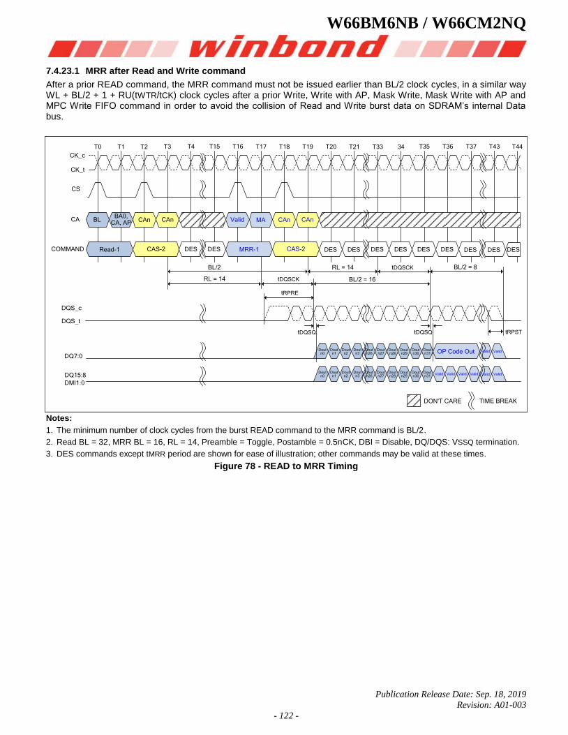
W66BM6NB / W66CM2NQ
Publication Release Date: Sep. 18, 2019
Revision: A01-003
- 122 -
7.4.23.1 MRR after Read and Write command
After a prior READ command, the MRR command must not be issued earlier than BL/2 clock cycles, in a similar way WL + BL/2 + 1 + RU(tWTR/tCK) clock cycles after a prior Write, Write with AP, Mask Write, Mask Write with AP and MPC Write FIFO command in order to avoid the collision of Read and Write burst data on SDRAM’s internal Data bus.
CK_c
CK_t
T0 T1 T2 T3 T4 T15 T16 T17 T18 T19 T20 T21 T33 34 T35 T36 T37 T43 T44
Read-1 CAS-2
BL CAnCAn
tRPST
tRPRE
RL = 14
DES DESDES DES DES DES DES DES DES DES DESCOMMAND
CS
CA
DON'T CARE TIME BREAK
Valid MA CAnCAn
BL/2
tDQSCK
BL/2 = 8
tDQSQ
DQS_c
DQS_t
DQ15:8
DMI1:0
DQ7:0
BA0,CA, AP
MRR-1 CAS-2
OP Code OutDout n31
Dout n30
Dout n29
Dout n28
Dout n27
Dout n26
Dout n3
Dout n2
Dout n1
Dout n0
ValidValidValidValidValid Valid
ValidValid
Dout n31
Dout n30
Dout n29
Dout n28
Dout n27
Dout n26
Dout n3
Dout n2
Dout n1
Dout n0
tDQSCKRL = 14
tDQSQ
BL/2 = 16
Notes:
1. The minimum number of clock cycles from the burst READ command to the MRR command is BL/2.
2. Read BL = 32, MRR BL = 16, RL = 14, Preamble = Toggle, Postamble = 0.5nCK, DBI = Disable, DQ/DQS: VSSQ termination.
3. DES commands except tMRR period are shown for ease of illustration; other commands may be valid at these times.
Figure 78 - READ to MRR Timing
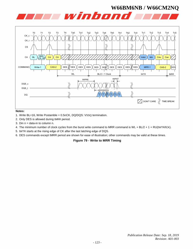
W66BM6NB / W66CM2NQ
Publication Release Date: Sep. 18, 2019
Revision: A01-003
- 123 -
CK_c
CK_t
T0 T1 T2 T3 T4 Ta0 Ta1 Ta2 Ta3 Ta4 Tb0 Tb1 Tb2 Tc0 Tc1 Tc2 Tc3 Tc4 Tc5
Write-1 CAS-2
BL CACA
tWPSTtWPRE
WL
DES DESDES DES DES DES DESDES DES DES DESCOMMAND
CS
CA Valid CanCAn
tWTR
tDQS2DQ
DQS_c
DQS_t
DQ
BA0,CA, AP
CAS-2MRR-1
MA
BL/2 + 1 Clock
Din n14
Din n15
Din n12
Din n13
Din n0
Din n1
tMRR
DON'T CARE TIME BREAK
Notes:
1. Write BL=16, Write Postamble = 0.5nCK, DQ/DQS: VSSQ termination.
2. Only DES is allowed during tMRR period.
3. Din n = data-in to column n.
4. The minimum number of clock cycles from the burst write command to MRR command is WL + BL/2 + 1 + RU(tWTR/tCK).
5. tWTR starts at the rising edge of CK after the last latching edge of DQS.
6. DES commands except tMRR period are shown for ease of illustration; other commands may be valid at these times.
Figure 79 - Write to MRR Timing
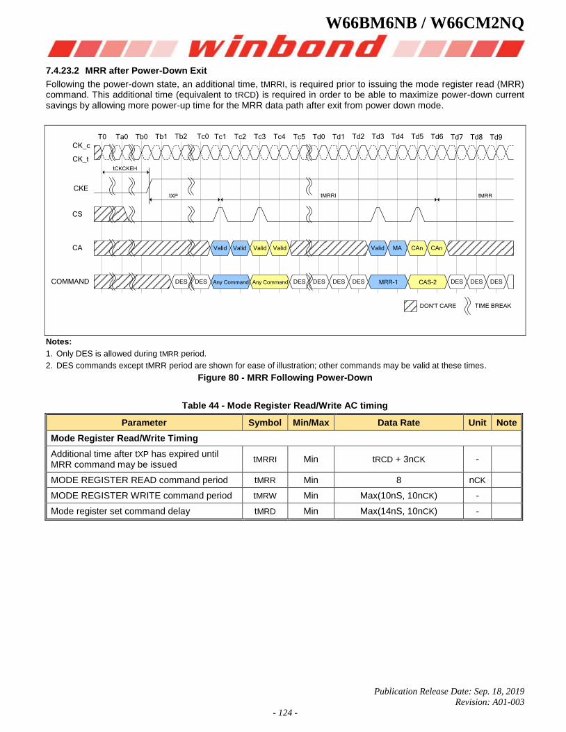
W66BM6NB / W66CM2NQ
Publication Release Date: Sep. 18, 2019
Revision: A01-003
- 124 -
7.4.23.2 MRR after Power-Down Exit
Following the power-down state, an additional time, tMRRI, is required prior to issuing the mode register read (MRR) command. This additional time (equivalent to tRCD) is required in order to be able to maximize power-down current savings by allowing more power-up time for the MRR data path after exit from power down mode.
Valid Valid Valid Valid Valid MA CAn CAn
DES DESDES DES DES DESAny Command DES
T0 Ta0 Tb0 Tb1 Tb2 Tc0 Tc1 Tc2 Tc3 Tc4 Tc5 Td0 Td1 Td2 Td3 Td4 Td5 Td6 Td7 Td8 Td9CK_c
CK_t
COMMAND
CA
CS
CKE
TIME BREAKDON'T CARE
tXP tMRRI
DES Any Command DES
tMRR
MRR-1 CAS-2
tCKCKEH
Notes:
1. Only DES is allowed during tMRR period.
2. DES commands except tMRR period are shown for ease of illustration; other commands may be valid at these times.
Figure 80 - MRR Following Power-Down
Table 44 - Mode Register Read/Write AC timing
Parameter Symbol Min/Max Data Rate Unit Note
Mode Register Read/Write Timing
Additional time after tXP has expired until MRR command may be issued
tMRRI Min tRCD + 3nCK -
MODE REGISTER READ command period tMRR Min 8 nCK
MODE REGISTER WRITE command period tMRW Min Max(10nS, 10nCK) -
Mode register set command delay tMRD Min Max(14nS, 10nCK) -
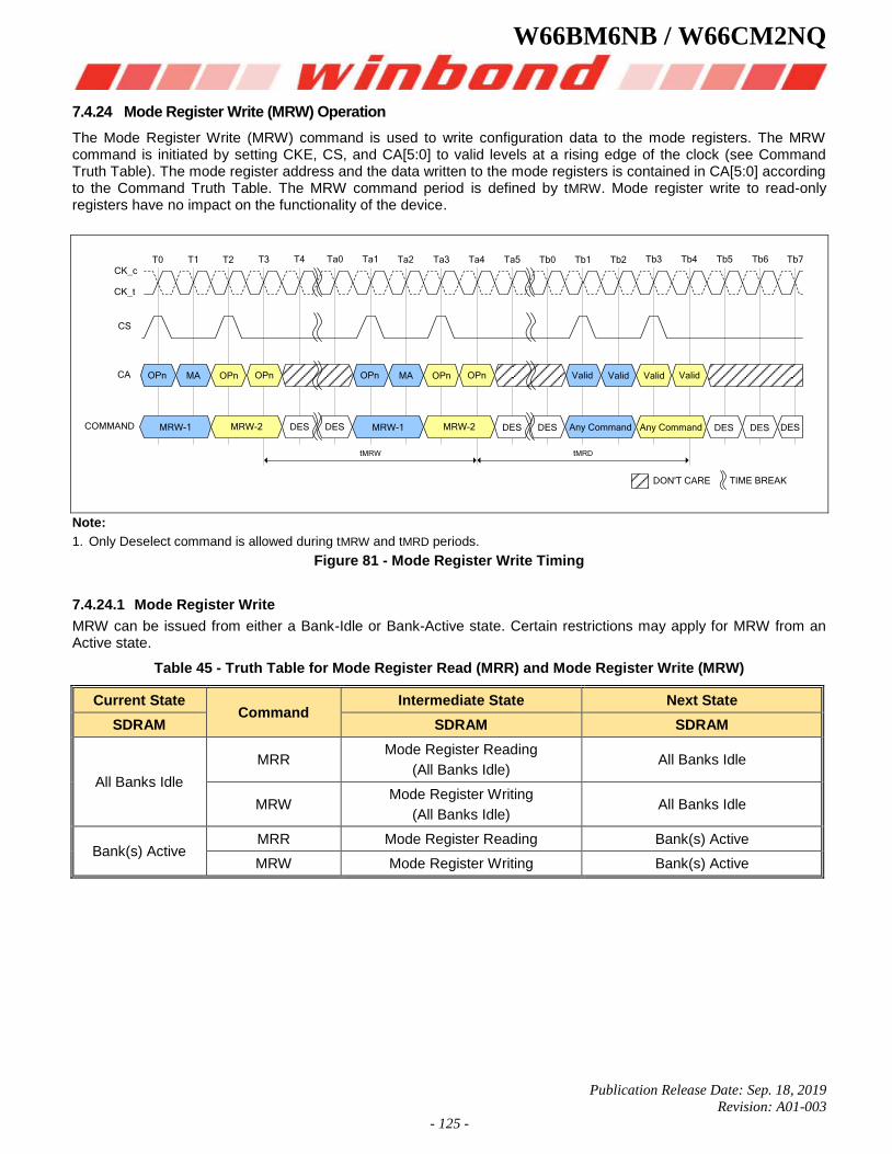
W66BM6NB / W66CM2NQ
Publication Release Date: Sep. 18, 2019
Revision: A01-003
- 125 -
7.4.24 Mode Register Write (MRW) Operation
The Mode Register Write (MRW) command is used to write configuration data to the mode registers. The MRW command is initiated by setting CKE, CS, and CA[5:0] to valid levels at a rising edge of the clock (see Command Truth Table). The mode register address and the data written to the mode registers is contained in CA[5:0] according to the Command Truth Table. The MRW command period is defined by tMRW. Mode register write to read-only registers have no impact on the functionality of the device.
CK_c
CK_t
COMMAND
T0 T1 T2 T3 T4 Ta0 Ta1 Ta2 Ta3 Ta4 Ta5 Tb0 Tb1 Tb2 Tb3 Tb4 Tb5 Tb6 Tb7
tMRW
OPn OPnOPnCA
CS
MRW-2 DES DES DES DES DES DES
tMRD
TIME BREAKDON'T CARE
MA OPn OPnOPnMA Valid ValidValidValid
MRW-1 MRW-2MRW-1 Any Command Any Command DES
Note:
1. Only Deselect command is allowed during tMRW and tMRD periods.
Figure 81 - Mode Register Write Timing
7.4.24.1 Mode Register Write
MRW can be issued from either a Bank-Idle or Bank-Active state. Certain restrictions may apply for MRW from an Active state.
Table 45 - Truth Table for Mode Register Read (MRR) and Mode Register Write (MRW)
Current State Command
Intermediate State Next State
SDRAM SDRAM SDRAM
All Banks Idle
MRR Mode Register Reading
(All Banks Idle) All Banks Idle
MRW Mode Register Writing
(All Banks Idle) All Banks Idle
Bank(s) Active MRR Mode Register Reading Bank(s) Active
MRW Mode Register Writing Bank(s) Active
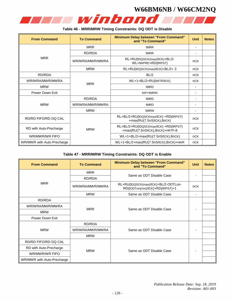
W66BM6NB / W66CM2NQ
Publication Release Date: Sep. 18, 2019
Revision: A01-003
- 126 -
Table 46 - MRR/MRW Timing Constraints: DQ ODT is Disable
From Command To Command Minimum Delay between "From Command"
and "To Command" Unit Notes
MRR
MRR tMRR -
RD/RDA tMRR -
WR/WRA/MWR/MWRA RL+RU(tDQSCK(max)/tCK)+BL/2-
WL+tWPRE+RD(tRPST) nCK
MRW RL+RU(tDQSCK(max)/tCK)+BL/2+ 3 nCK
RD/RDA
MRR
BL/2 nCK
WR/WRA/MWR/MWRA WL+1+BL/2+RU(tWTR/tCK) nCK
MRW tMRD -
Power Down Exit tXP+tMRRI -
MRW
RD/RDA tMRD -
WR/WRA/MWR/MWRA tMRD -
MRW tMRW -
RD/RD FIFO/RD DQ CAL
MRW
RL+BL/2+RU(tDQSCKmax/tCK) +RD(tRPST) +max(RU(7.5nS/tCK),8nCK)
nCK
RD with Auto-Precharge RL+BL/2+RU(tDQSCKmax/tCK) +RD(tRPST)
+max(RU(7.5nS/tCK),8nCK)+nRTP-8 nCK
WR/MWR/WR FIFO WL+1+BL/2+max(RU(7.5nS/tCK),8nCK) nCK
WR/MWR with Auto-Precharge WL+1+BL/2+max(RU(7.5nS/tCK),8nCK)+nWR nCK
Table 47 - MRR/MRW Timing Constraints: DQ ODT is Enable
From Command To Command Minimum Delay between "From Command"
and "To Command" Unit Notes
MRR
MRR Same as ODT Disable Case -
RD/RDA
WR/WRA/MWR/MWRA RL+RU(tDQSCK(max)/tCK)+BL/2-ODTLon-
RD(tODTon(min)/tCK)+RD(tRPST)+1 nCK
MRW Same as ODT Disable Case -
RD/RDA
MRR Same as ODT Disable Case -
WR/WRA/MWR/MWRA
MRW
Power Down Exit
MRW
RD/RDA
Same as ODT Disable Case -
WR/WRA/MWR/MWRA
MRW
RD/RD FIFO/RD DQ CAL
MRW Same as ODT Disable Case -
RD with Auto-Precharge
WR/MWR/WR FIFO
WR/MWR with Auto-Precharge
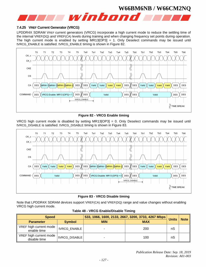
W66BM6NB / W66CM2NQ
Publication Release Date: Sep. 18, 2019
Revision: A01-003
- 127 -
7.4.25 VREF Current Generator (VRCG)
LPDDR4X SDRAM VREF current generators (VRCG) incorporate a high current mode to reduce the settling time of the internal VREF(DQ) and VREF(CA) levels during training and when changing frequency set points during operation. The high current mode is enabled by setting MR13[OP3] = 1. Only Deselect commands may be issued until tVRCG_ENABLE is satisfied. tVRCG_ENABLE timing is shown in Figure 82.
CK_c
CK_t
COMMAND
T0 T1 T2 T3 T4 T5 Ta0 Ta1 Ta2 Ta3 Ta4 Ta5 Tb0 Tb1 Tb2 Tb3 Tb4 Tb5 Tb6
tVRCG_ENABLE
MRW-1CA
CS
DES DES DES DESDES DES
TIME BREAK
Valid ValidValidValid Valid ValidValidValid
CKE
MRW-1 MRW-2 MRW-2 DES DES DES DES DESDES
Valid ValidVRCG Enable: MR13 [OP3] = 1
DES
DES
Figure 82 - VRCG Enable timing
VRCG high current mode is disabled by setting MR13[OP3] = 0. Only Deselect commands may be issued until tVRCG_DISABLE is satisfied. tVRCG_DISABLE timing is shown in Figure 83.
CK_c
CK_t
COMMAND
T0 T1 T2 T3 T4 T5 Ta0 Ta1 Ta2 Ta3 Ta4 Ta5 Tb0 Tb1 Tb2 Tb3 Tb4 Tb5 Tb6
tVRCG_DISABLE
CA
CS
DES DES DES DESDES DES
TIME BREAK
Valid ValidValidValid Valid ValidValidValid
CKE
MRW-1 MRW-2 MRW-2DES DES DES DES DESDES
Valid ValidVRCG Disable: MR13 [OP3] = 0
DES
DES
MRW-1
Figure 83 - VRCG Disable timing
Note that LPDDR4X SDRAM devices support VREF(CA) and VREF(DQ) range and value changes without enabling VRCG high current mode.
Table 48 - VRCG Enable/Disable Timing
Speed 533, 1066, 1600, 2133, 2667, 3200, 3733, 4267 Mbps Units Note
Parameter Symbol MIN MAX
VREF high current mode enable time
tVRCG_ENABLE - 200 nS
VREF high current mode disable time
tVRCG_DISABLE - 100 nS
W66BM6NB / W66CM2NQ
Publication Release Date: Sep. 18, 2019
Revision: A01-003
- 128 -
7.4.26 CA VREF Training
The DRAM internal CA VREF specification parameters are voltage operating range, step size, VREF set tolerance, VREF step time and VREF valid level.
The voltage operating range specifies the minimum required VREF setting range for LPDDR4X DRAM devices. The minimum range is defined by VREFmax and VREFmin as depicted in Figure 84.
Total Range
System VarianceVswing Small
Vswing Large
VREF
Range
VREFmax
VREFmin
Vin DC Low
Vin DC max
VDD2
Figure 84 - VREF operating range (VREFmin, VREFmax)
The VREF step size is defined as the step size between adjacent steps. However, for a given design, DRAM has one value for VREF step size that falls within the range.
The VREF set tolerance is the variation in the VREF voltage from the ideal setting. This accounts for accumulated error over multiple steps. There are two ranges for VREF set tolerance uncertainty. The range of VREF set tolerance uncertainty is a function of number of steps n.
The VREF set tolerance is measured with respect to the ideal line which is based on the two endpoints. Where the endpoints are at the min and max VREF values for a specified range. An example of the step size and VREF set tolerance is shown in Figure 85.
Digital Code
VREF
VREF Set
Tolerance
Actual VREF
Output
Straight Line
(endpoint Fit)
VREF
Step size
Figure 85 - Example of VREF set tolerance (max case only shown) and step size
W66BM6NB / W66CM2NQ
Publication Release Date: Sep. 18, 2019
Revision: A01-003
- 129 -
The VREF increment/decrement step times are define by VREF_time-short, Middle and long. The VREF_time-short, VREF_time-Middle and VREF_time-long is defined from TS to TE as shown in Figure 86 where TE is referenced to when the VREF voltage is at the final DC level within the VREF valid tolerance(VREF_val_tol).
The VREF valid level is defined by VREF_val tolerance to qualify the step time TE as shown in Figure 86.
This parameter is used to insure an adequate RC time constant behavior of the voltage level change after any VREF increment/decrement adjustment. This parameter is only applicable for DRAM component level validation/characterization.
VREF_time-Short is for a single step size increment/decrement change in VREF voltage.
VREF_time-Middle is at least 2 step sizes increment/decrement change within the same VREFCA range in VREF voltage.
VREF_time-Long is the time including up to VREFmin to VREFmax or VREFmax to VREFmin change across the VREFCA Range in VREF voltage.
TS - is referenced to MRS command clock
TE - is referenced to the VREF_val_tol
CK_c
CK_t
T0 T1 T2 T3 T4 T5 Ta0 Ta1 Ta2 Ta3 Ta4 Ta5 Ta6 Ta7 Ta8 Ta9 Ta10 Ta11 Ta12
MRW-1
DES DES DES DES DES DESDES DES DES DESCOMMAND
CS
CA DES DESDES
TS
VRFF Setting
Adjustment
DES
VREF_time-Short/Middle/Long
TIME BREAK
CKE
Old VREF Setting Updating VREF(CA) Setting New VREF Setting
DES DES DES DES DESDES DES DES DESDES MRW-1 MRW-2 MRW-2 DES
VRFF(CA) Value/Range Set DES DESDESDES DES
TE
Figure 86 - VREF_time for Short, Middle and Long Timing Diagram
The MRW command to the mode register bits are as follows.
MR12 OP[5:0]: VREF(CA) Setting
MR12 OP[6]: VREF(CA) Range
W66BM6NB / W66CM2NQ
Publication Release Date: Sep. 18, 2019
Revision: A01-003
- 130 -
The minimum time required between two VREF MRS commands is VREF_time-short for single step and VREF_time-Middle for a full voltage range step.
Step size
VRFF
Voltage
VRFF DC
(VDD2 DC)
VRFF_val_tol
t1
Time
Figure 87 - VREF step single step size increment case
Step size
VRFF
Voltage
VRFF DC
(VDD2 DC)
VRFF_val_tol
t1
Time
Figure 88 - VREF step single step size decrement case

W66BM6NB / W66CM2NQ
Publication Release Date: Sep. 18, 2019
Revision: A01-003
- 131 -
VREF
VoltageVREF DC
(VDD2 DC)VREFmax
VREF_val_tol
t1
Time
VREFmin
Full
Range
Step
Figure 89 - VREF full step from VREFmin to VREFmax case
VREF
Voltage
VREF DC
VREFmax
VREF_val_tol
t1
Time
VREFmin
Full
Range
Step
(VDD2 DC)
Figure 90 - VREF full step from VREFmax to VREFmin case
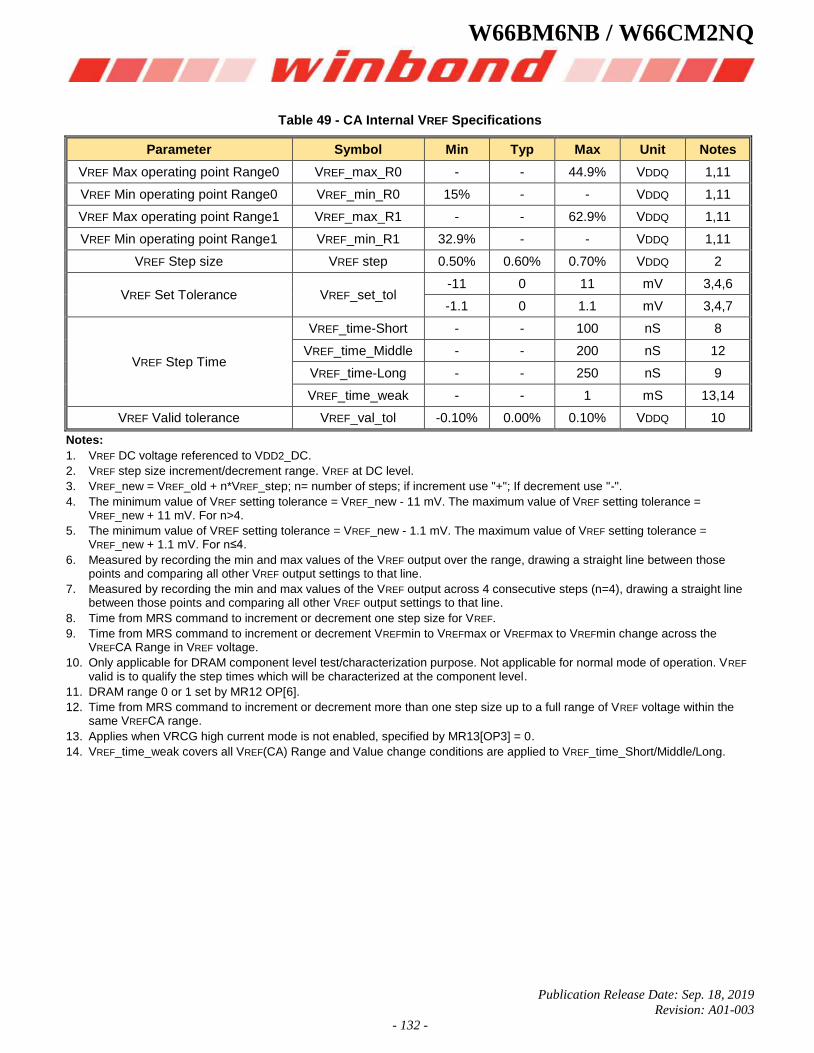
W66BM6NB / W66CM2NQ
Publication Release Date: Sep. 18, 2019
Revision: A01-003
- 132 -
Table 49 - CA Internal VREF Specifications
Parameter Symbol Min Typ Max Unit Notes
VREF Max operating point Range0 VREF_max_R0 - - 44.9% VDDQ 1,11
VREF Min operating point Range0 VREF_min_R0 15% - - VDDQ 1,11
VREF Max operating point Range1 VREF_max_R1 - - 62.9% VDDQ 1,11
VREF Min operating point Range1 VREF_min_R1 32.9% - - VDDQ 1,11
VREF Step size VREF step 0.50% 0.60% 0.70% VDDQ 2
VREF Set Tolerance VREF_set_tol -11 0 11 mV 3,4,6
-1.1 0 1.1 mV 3,4,7
VREF Step Time
VREF_time-Short - - 100 nS 8
VREF_time_Middle - - 200 nS 12
VREF_time-Long - - 250 nS 9
VREF_time_weak - - 1 mS 13,14
VREF Valid tolerance VREF_val_tol -0.10% 0.00% 0.10% VDDQ 10
Notes:
1. VREF DC voltage referenced to VDD2_DC.
2. VREF step size increment/decrement range. VREF at DC level.
3. VREF_new = VREF_old + n*VREF_step; n= number of steps; if increment use "+"; If decrement use "-".
4. The minimum value of VREF setting tolerance = VREF_new - 11 mV. The maximum value of VREF setting tolerance = VREF_new + 11 mV. For n>4.
5. The minimum value of VREF setting tolerance = VREF_new - 1.1 mV. The maximum value of VREF setting tolerance = VREF_new + 1.1 mV. For n≤4.
6. Measured by recording the min and max values of the VREF output over the range, drawing a straight line between those points and comparing all other VREF output settings to that line.
7. Measured by recording the min and max values of the VREF output across 4 consecutive steps (n=4), drawing a straight line between those points and comparing all other VREF output settings to that line.
8. Time from MRS command to increment or decrement one step size for VREF.
9. Time from MRS command to increment or decrement VREFmin to VREFmax or VREFmax to VREFmin change across the VREFCA Range in VREF voltage.
10. Only applicable for DRAM component level test/characterization purpose. Not applicable for normal mode of operation. VREF valid is to qualify the step times which will be characterized at the component level.
11. DRAM range 0 or 1 set by MR12 OP[6].
12. Time from MRS command to increment or decrement more than one step size up to a full range of VREF voltage within the same VREFCA range.
13. Applies when VRCG high current mode is not enabled, specified by MR13[OP3] = 0.
14. VREF_time_weak covers all VREF(CA) Range and Value change conditions are applied to VREF_time_Short/Middle/Long.
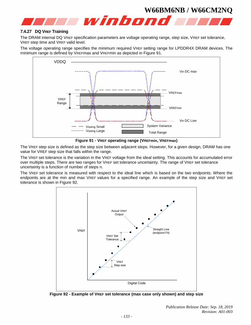
W66BM6NB / W66CM2NQ
Publication Release Date: Sep. 18, 2019
Revision: A01-003
- 133 -
7.4.27 DQ VREF Training
The DRAM internal DQ VREF specification parameters are voltage operating range, step size, VREF set tolerance, VREF step time and VREF valid level.
The voltage operating range specifies the minimum required VREF setting range for LPDDR4X DRAM devices. The minimum range is defined by VREFmax and VREFmin as depicted in Figure 91.
Total Range
System VarianceVswing Small
Vswing Large
VREF
Range
VREFmax
VREFmin
Vin DC Low
Vin DC max
VDDQ
Figure 91 - VREF operating range (VREFmin, VREFmax)
The VREF step size is defined as the step size between adjacent steps. However, for a given design, DRAM has one value for VREF step size that falls within the range.
The VREF set tolerance is the variation in the VREF voltage from the ideal setting. This accounts for accumulated error over multiple steps. There are two ranges for VREF set tolerance uncertainty. The range of VREF set tolerance uncertainty is a function of number of steps n.
The VREF set tolerance is measured with respect to the ideal line which is based on the two endpoints. Where the endpoints are at the min and max VREF values for a specified range. An example of the step size and VREF set tolerance is shown in Figure 92.
Digital Code
VREF
VREF Set
Tolerance
Actual VREF
Output
Straight Line
(endpoint Fit)
VREF
Step size
Figure 92 - Example of VREF set tolerance (max case only shown) and step size

W66BM6NB / W66CM2NQ
Publication Release Date: Sep. 18, 2019
Revision: A01-003
- 134 -
The VREF increment/decrement step times are define by VREF_time-short, Middle and long. The VREF_time-short, VREF_time-Middle and VREF_time-long is defined from TS to TE as shown in Figure 93 where TE is referenced to when the VREF voltage is at the final DC level within the VREF valid tolerance(VREF_val_tol).
The VREF valid level is defined by VREF_val tolerance to qualify the step time TE as shown in Figure 93.
This parameter is used to insure an adequate RC time constant behavior of the voltage level change after any VREF increment/decrement adjustment. This parameter is only applicable for DRAM component level validation/characterization.
VREF_time-Short is for a single step size increment/decrement change in VREF voltage.
VREF_time-Middle is at least 2 step sizes increment/decrement change within the same VREFDQ range in VREF voltage.
VREF_time-Long is the time including up to VREFmin to VREFmax or VREFmax to VREFmin change across the VREFDQ Range in VREF voltage.
TS - is referenced to MRS command clock
TE - is referenced to the VREF_val_tol
CK_c
CK_t
T0 T1 T2 T3 T4 T5 Ta0 Ta1 Ta2 Ta3 Ta4 Ta5 Ta6 Ta7 Ta8 Ta9 Ta10 Ta11 Ta12
MRW-1
DES DES DES DES DES DESDES DES DES DESCOMMAND
CS
CA DES DESDES
TS
VRFF Setting
Adjustment
DES
VREF_time-Short/Middle/Long
TIME BREAK
CKE
Old VREF Setting Updating VREF(DQ) Setting New VREF Setting
DES DES DES DES DESDES DES DES DESDES MRW-1 MRW-2 MRW-2 DES
VRFF(DQ) Value/Range Set DES DESDESDES DES
TE
Figure 93 - VREF_time for Short, Middle and Long Timing Diagram
The MRW command to the mode register bits are as follows.
MR14 OP[5:0]: VREF(DQ) Setting
MR14 OP[6]: VREF(DQ) Range

W66BM6NB / W66CM2NQ
Publication Release Date: Sep. 18, 2019
Revision: A01-003
- 135 -
The minimum time required between two VREF MRS commands is VREF_time-short for single step and VREF_time-Middle for a full voltage range step.
Step size
VRFF
Voltage
VRFF DC
(VDDQ DC)
VRFF_val_tol
t1
Time
Figure 94 - VREF step single step size increment case
Step size
VRFF
Voltage
VRFF DC
(VDDQ DC)
VRFF_val_tol
t1
Time
Figure 95 - VREF step single step size decrement case
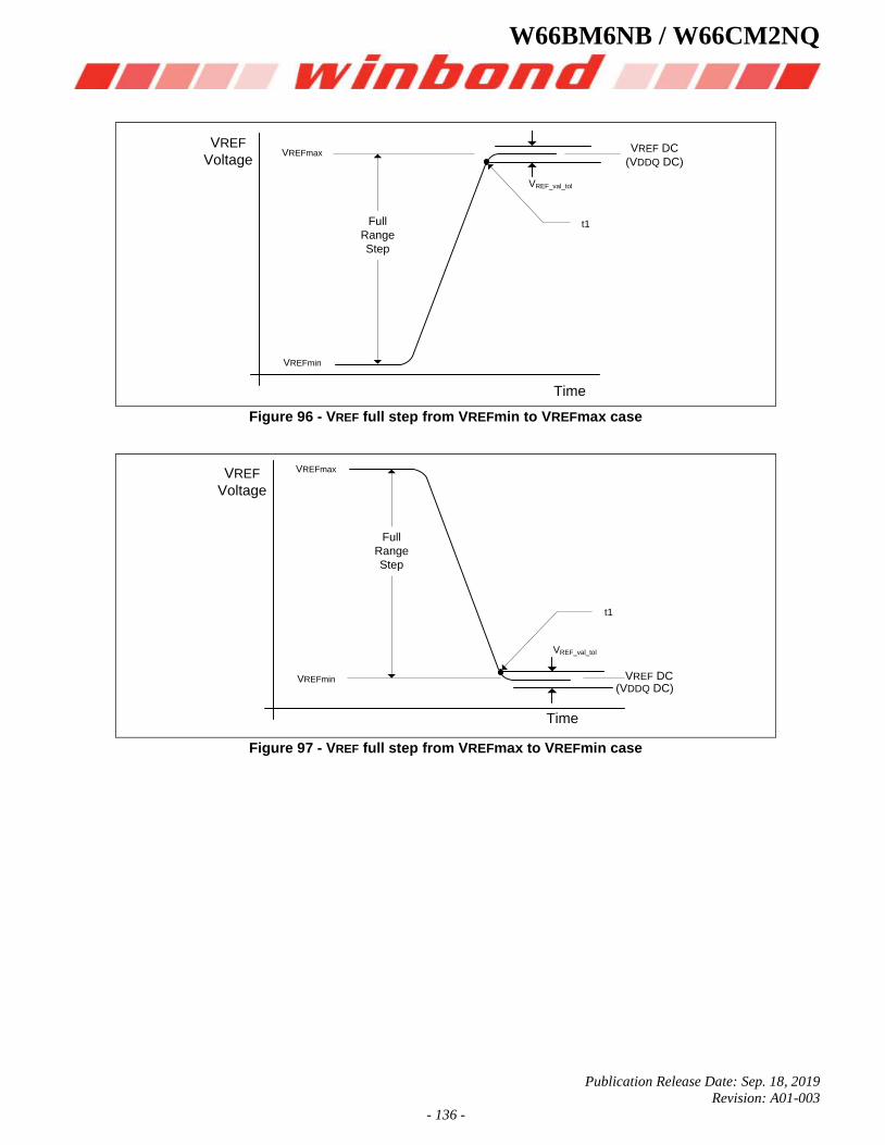
W66BM6NB / W66CM2NQ
Publication Release Date: Sep. 18, 2019
Revision: A01-003
- 136 -
VREF
VoltageVREF DC
(VDDQ DC)VREFmax
VREF_val_tol
t1
Time
VREFmin
Full
Range
Step
Figure 96 - VREF full step from VREFmin to VREFmax case
VREF
Voltage
VREF DC
VREFmax
VREF_val_tol
t1
Time
VREFmin
Full
Range
Step
(VDDQ DC)
Figure 97 - VREF full step from VREFmax to VREFmin case
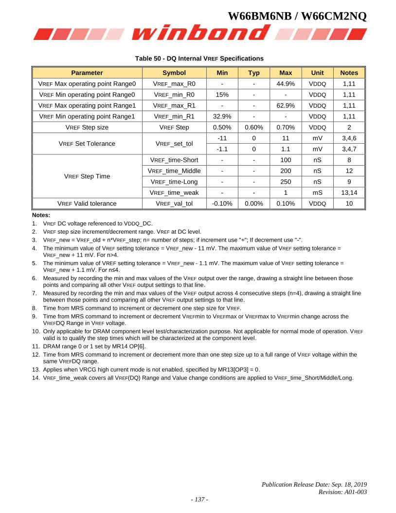
W66BM6NB / W66CM2NQ
Publication Release Date: Sep. 18, 2019
Revision: A01-003
- 137 -
Table 50 - DQ Internal VREF Specifications
Parameter Symbol Min Typ Max Unit Notes
VREF Max operating point Range0 VREF_max_R0 - - 44.9% VDDQ 1,11
VREF Min operating point Range0 VREF_min_R0 15% - - VDDQ 1,11
VREF Max operating point Range1 VREF_max_R1 - - 62.9% VDDQ 1,11
VREF Min operating point Range1 VREF_min_R1 32.9% - - VDDQ 1,11
VREF Step size VREF Step 0.50% 0.60% 0.70% VDDQ 2
VREF Set Tolerance VREF_set_tol -11 0 11 mV 3,4,6
-1.1 0 1.1 mV 3,4,7
VREF Step Time
VREF_time-Short - - 100 nS 8
VREF_time_Middle - - 200 nS 12
VREF_time-Long - - 250 nS 9
VREF_time_weak - - 1 mS 13,14
VREF Valid tolerance VREF_val_tol -0.10% 0.00% 0.10% VDDQ 10
Notes:
1. VREF DC voltage referenced to VDDQ_DC.
2. VREF step size increment/decrement range. VREF at DC level.
3. VREF_new = VREF_old + n*VREF_step; n= number of steps; if increment use "+"; If decrement use "-".
4. The minimum value of VREF setting tolerance = VREF_new - 11 mV. The maximum value of VREF setting tolerance = VREF_new + 11 mV. For n>4.
5. The minimum value of VREF setting tolerance = VREF_new - 1.1 mV. The maximum value of VREF setting tolerance = VREF_new + 1.1 mV. For n≤4.
6. Measured by recording the min and max values of the VREF output over the range, drawing a straight line between those points and comparing all other VREF output settings to that line.
7. Measured by recording the min and max values of the VREF output across 4 consecutive steps (n=4), drawing a straight line between those points and comparing all other VREF output settings to that line.
8. Time from MRS command to increment or decrement one step size for VREF.
9. Time from MRS command to increment or decrement VREFmin to VREFmax or VREFmax to VREFmin change across the VREFDQ Range in VREF voltage.
10. Only applicable for DRAM component level test/characterization purpose. Not applicable for normal mode of operation. VREF valid is to qualify the step times which will be characterized at the component level.
11. DRAM range 0 or 1 set by MR14 OP[6].
12. Time from MRS command to increment or decrement more than one step size up to a full range of VREF voltage within the same VREFDQ range.
13. Applies when VRCG high current mode is not enabled, specified by MR13[OP3] = 0.
14. VREF_time_weak covers all VREF(DQ) Range and Value change conditions are applied to VREF_time_Short/Middle/Long.
W66BM6NB / W66CM2NQ
Publication Release Date: Sep. 18, 2019
Revision: A01-003
- 138 -
7.4.28 Command Bus Training
The LPDDR4X-SDRAM command bus must be trained before enabling termination for high-frequency operation. LPDDR4X provides an internal VREF(CA) that defaults to a level suitable for un-terminated, low frequency operation, but the VREF(CA) must be trained to achieve suitable receiver voltage margin for terminated, high-frequency operation. The training mode described here centers the internal VREF(CA) in the CA data eye and at the same time allows for timing adjustments of the CS and CA signals to meet setup/hold requirements. Because it can be difficult to capture commands prior to training the CA inputs, the training mode described here uses a minimum of external commands to enter, train, and exit the Command Bus Training mode.
NOTE: It is up to the system designer to determine what constitutes “low-frequency” and “high-frequency” based on the
capabilities of the system. Low-frequency should then be defined as an operating frequency in which the system can reliably communicate with the SDRAM before Command Bus Training is executed.
The LPDDR4X-SDRAM die has a bond pad (ODT_CA) for multi-rank operation. In a multi-rank system, the terminating rank should be trained first, followed by the non-terminating rank(s). See 7.4.40.1, ODT section for more information.
The LPDDR4X-SDRAM uses Frequency Set-Points to enable multiple operating settings for the die. The LPDDR4X-SDRAM defaults to FSP-OP[0] at power-up, which has the default settings to operate in unterminated, low-frequency environments. Prior to training, the mode register settings should be configured by setting MR13 OP[6]=1B (FSP-
WR[1]) and setting all other mode register bits for FSP-OP[1] to the desired settings for high-frequency operation. Prior to entering Command Bus Training, the SDRAM will be operating from FSP-OP[x]. Upon Command Bus Training entry when CKE is driven LOW, the LPDDR4X-SDRAM will automatically switch to the alternate FSP register set (FSP-OP[y]) and use the alternate register settings during training (See note 6 in Figure 99 for more information on FSP-OP register sets). Upon training exit when CKE is driven HIGH, the LPDDR4X-SDRAM will automatically switch back to the original FSP register set (FSP-OP[x]), returning to the “known-good” state that was operating prior to training. The training values for VREF(CA) are not retained by the DRAM in FSP-OP[y] registers, and must be written to the registers after training exit.
1. To enter Command Bus Training mode, issue a MRW-1 command followed by a MRW-2 command to set MR13 OP[0]=1B (Command Bus Training Mode Enabled).
2. After time tMRD, CKE may be set LOW, causing the LPDDR4X-SDRAM to switch from FSP-OP[x] to FSP-OP[y], and completing the entry into Command Bus Training mode.
A status of DQS_t, DQS_c, DQ and DMI are as follows, and DQ ODT state will be followed Frequency Set Point function except output pins.
- DQS_t[0], DQS_c[0] become input pins for capturing DQ[6:0] levels by its toggling.
- DQ[5:0] become input pins for setting VREF(CA) Level.
- DQ[6] becomes input pin for setting VREF(CA) Range.
- DQ[7] and DMI[0] become input pins and their input level is Valid level or floating, either way is fine.
- DQ[13:8] become output pins to feedback its capturing value via command bus by CS signal.
- DQS_t[1], DQS_c[1],DMI[1] and DQ[15:14] become output pins or disable, it means that SDRAM may drive to a valid level or left floating.
3. At time tCAENT later, LPDDR4X SDRAM can accept to change its VREF(CA) Range and Value using input signals of DQS_t[0], DQS_c[0] and DQ[6:0] from existing value that’s setting via MR12 OP[6:0]. The mapping between MR12 OP code and DQs is shown in Table 51. At least one VREFCA setting is required before proceed to next training steps.
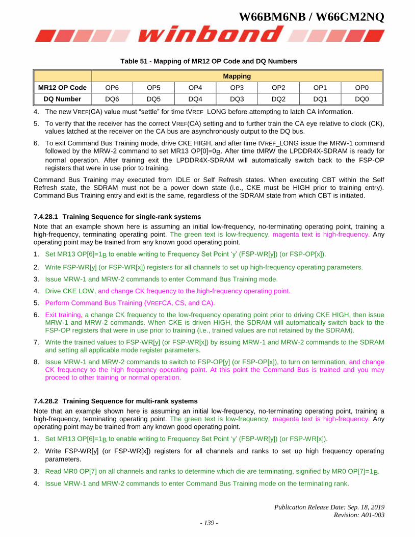
W66BM6NB / W66CM2NQ
Publication Release Date: Sep. 18, 2019
Revision: A01-003
- 139 -
Table 51 - Mapping of MR12 OP Code and DQ Numbers
Mapping
MR12 OP Code OP6 OP5 OP4 OP3 OP2 OP1 OP0
DQ Number DQ6 DQ5 DQ4 DQ3 DQ2 DQ1 DQ0
4. The new VREF(CA) value must “settle” for time tVREF_LONG before attempting to latch CA information.
5. To verify that the receiver has the correct VREF(CA) setting and to further train the CA eye relative to clock (CK), values latched at the receiver on the CA bus are asynchronously output to the DQ bus.
6. To exit Command Bus Training mode, drive CKE HIGH, and after time tVREF_LONG issue the MRW-1 command followed by the MRW-2 command to set MR13 OP[0]=0B. After time tMRW the LPDDR4X-SDRAM is ready for
normal operation. After training exit the LPDDR4X-SDRAM will automatically switch back to the FSP-OP registers that were in use prior to training.
Command Bus Training may executed from IDLE or Self Refresh states. When executing CBT within the Self Refresh state, the SDRAM must not be a power down state (i.e., CKE must be HIGH prior to training entry). Command Bus Training entry and exit is the same, regardless of the SDRAM state from which CBT is initiated.
7.4.28.1 Training Sequence for single-rank systems
Note that an example shown here is assuming an initial low-frequency, no-terminating operating point, training a high-frequency, terminating operating point. The green text is low-frequency, magenta text is high-frequency. Any operating point may be trained from any known good operating point.
1. Set MR13 OP[6]=1B to enable writing to Frequency Set Point ‘y’ (FSP-WR[y]) (or FSP-OP[x]).
2. Write FSP-WR[y] (or FSP-WR[x]) registers for all channels to set up high-frequency operating parameters.
3. Issue MRW-1 and MRW-2 commands to enter Command Bus Training mode.
4. Drive CKE LOW, and change CK frequency to the high-frequency operating point.
5. Perform Command Bus Training (VREFCA, CS, and CA).
6. Exit training, a change CK frequency to the low-frequency operating point prior to driving CKE HIGH, then issue MRW-1 and MRW-2 commands. When CKE is driven HIGH, the SDRAM will automatically switch back to the FSP-OP registers that were in use prior to training (i.e., trained values are not retained by the SDRAM).
7. Write the trained values to FSP-WR[y] (or FSP-WR[x]) by issuing MRW-1 and MRW-2 commands to the SDRAM and setting all applicable mode register parameters.
8. Issue MRW-1 and MRW-2 commands to switch to FSP-OP[y] (or FSP-OP[x]), to turn on termination, and change CK frequency to the high frequency operating point. At this point the Command Bus is trained and you may proceed to other training or normal operation.
7.4.28.2 Training Sequence for multi-rank systems
Note that an example shown here is assuming an initial low-frequency, no-terminating operating point, training a high-frequency, terminating operating point. The green text is low-frequency, magenta text is high-frequency. Any operating point may be trained from any known good operating point.
1. Set MR13 OP[6]=1B to enable writing to Frequency Set Point ‘y’ (FSP-WR[y]) (or FSP-WR[x]).
2. Write FSP-WR[y] (or FSP-WR[x]) registers for all channels and ranks to set up high frequency operating
parameters.
3. Read MR0 OP[7] on all channels and ranks to determine which die are terminating, signified by MR0 OP[7]=1B.
4. Issue MRW-1 and MRW-2 commands to enter Command Bus Training mode on the terminating rank.
W66BM6NB / W66CM2NQ
Publication Release Date: Sep. 18, 2019
Revision: A01-003
- 140 -
5. Drive CKE LOW on the terminating rank (or all ranks), and change CK frequency to the high-frequency operating
point.
6. Perform Command Bus Training on the terminating rank (VREFCA, CS, and CA).
7. Exit training by driving CKE HIGH, change CK frequency to the low-frequency operating point, and issue MRW-1
and MRW-2 commands to write the trained values to FSP-W[y] (or FSP-WR[x]). When CKE is driven HIGH, the
SDRAM will automatically switch back to the FSP-OP registers that were in use prior to training (i.e., trained
values are not retained by the SDRAM).
8. Issue MRW-1 and MRW-2 command to enter training mode on the non-terminating rank (but keep CKE HIGH)
9. Issue MRW-1 and MRW-2 commands to switch the terminating rank to FSP-OP[y] (or FSP-OP[x]), to turn on
termination, and change CK frequency to the high frequency operating point.
10. Drive CKE LOW on the non-terminating (or all) ranks. The non-terminating rank(s) will now be using FSP-OP[y]
(or FSP-OP[x]).
11. Perform Command Bus Training on the non-terminating rank (VREFCA, CS, and CA).
12. Issue MRW-1 and MRW-2 commands to switch the terminating rank to FSP-OP[x] (or FSP-OP[y]) to turn off
termination.
13. Exit training by driving CKE HIGH on the non-terminating rank, change CK frequency to the low frequency
operating point, and issue MRW-1 and MRW-2 commands. When CKE is driven HIGH, the SDRAM will
automatically switch back to the FSP-OP registers that were in use prior to training (i.e., trained values are not
retained by the SDRAM).
14. Write the trained values to FSP-WR[y] (or FSP-WR[x]) by issuing MRW-1 and MRW-2 commands to the SDRAM
and setting all applicable mode register parameters.
15. Issue MRW-1 and MRW-2 commands to switch the terminating rank to FSP-OP[y] (or FSP-OP[x]), to turn on termination, and change CK frequency to the high frequency operating point. At this point the Command Bus is trained for both ranks and you may proceed to other training or normal operation.
7.4.28.3 Relation between CA input pin DQ output pin
The relation between CA input pin DQ output pin is shown in Table 52.
Table 52 - Mapping of CA Input pin and DQ Output pin
Mapping
CA Number CA5 CA4 CA3 CA2 CA1 CA0
DQ Number DQ13 DQ12 DQ11 DQ10 DQ9 DQ8
7.4.28.4 Timing Diagram
The basic Timing diagrams of Command Bus Training are shown in Figure 98, Figure 99, Figure 100, and Figure 101.
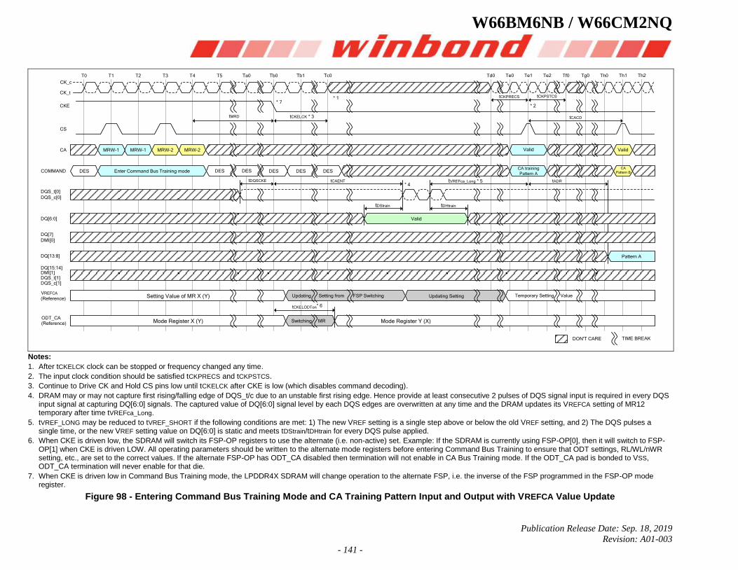
W66BM6NB / W66CM2NQ
Publication Release Date: Sep. 18, 2019
Revision: A01-003
- 141 -
T0 T1 T2 T3 T5T4 Ta0 Tb0 Tb1 Tc0 Td0 Te0 Te1 Te2 Tf0 Tg0 Th0 Th1 Th2
TIME BREAKDON'T CARE
MRW-1 MRW-1 MRW-2 MRW-2 Valid Valid
DES Enter Command Bus Training mode DES DES DES DES DESCA training
Pattern A
CA
Pattern B
Valid
Pattern A
CK_c
CK_t
CKE
CS
CA
COMMAND
DQS_t[0]
DQS_c[0]
DQ[6:0]
DQ[7]
DMI[0]
DQ[13:8]
DQ[15:14]DMI[1]DQS_t[1]DQS_c[1]
VREFCA
(Reference)
ODT_CA(Reference)
Updating Setting from FSP Switching Updating Setting
Switching MRMode Register X (Y) Mode Register Y (X)
Setting Value of MR X (Y)
tMRD
* 7* 1
tCKELCK * 3
* 2
tCKPRECS tCKPSTCS
tCACD
tADRtVREFca_Long * 5tCAENT
tDStrain tDHtrain
* 4tDQSCKE
Temporary Setting Value
tCKELODTon* 6
Notes:
1. After tCKELCK clock can be stopped or frequency changed any time.
2. The input clock condition should be satisfied tCKPRECS and tCKPSTCS.
3. Continue to Drive CK and Hold CS pins low until tCKELCK after CKE is low (which disables command decoding).
4. DRAM may or may not capture first rising/falling edge of DQS_t/c due to an unstable first rising edge. Hence provide at least consecutive 2 pulses of DQS signal input is required in every DQS input signal at capturing DQ[6:0] signals. The captured value of DQ[6:0] signal level by each DQS edges are overwritten at any time and the DRAM updates its VREFCA setting of MR12 temporary after time tVREFca_Long.
5. tVREF_LONG may be reduced to tVREF_SHORT if the following conditions are met: 1) The new VREF setting is a single step above or below the old VREF setting, and 2) The DQS pulses a single time, or the new VREF setting value on DQ[6:0] is static and meets tDStrain/tDHtrain for every DQS pulse applied.
6. When CKE is driven low, the SDRAM will switch its FSP-OP registers to use the alternate (i.e. non-active) set. Example: If the SDRAM is currently using FSP-OP[0], then it will switch to FSP-OP[1] when CKE is driven LOW. All operating parameters should be written to the alternate mode registers before entering Command Bus Training to ensure that ODT settings, RL/WL/nWR setting, etc., are set to the correct values. If the alternate FSP-OP has ODT_CA disabled then termination will not enable in CA Bus Training mode. If the ODT_CA pad is bonded to VSS, ODT_CA termination will never enable for that die.
7. When CKE is driven low in Command Bus Training mode, the LPDDR4X SDRAM will change operation to the alternate FSP, i.e. the inverse of the FSP programmed in the FSP-OP mode register.
Figure 98 - Entering Command Bus Training Mode and CA Training Pattern Input and Output with VREFCA Value Update
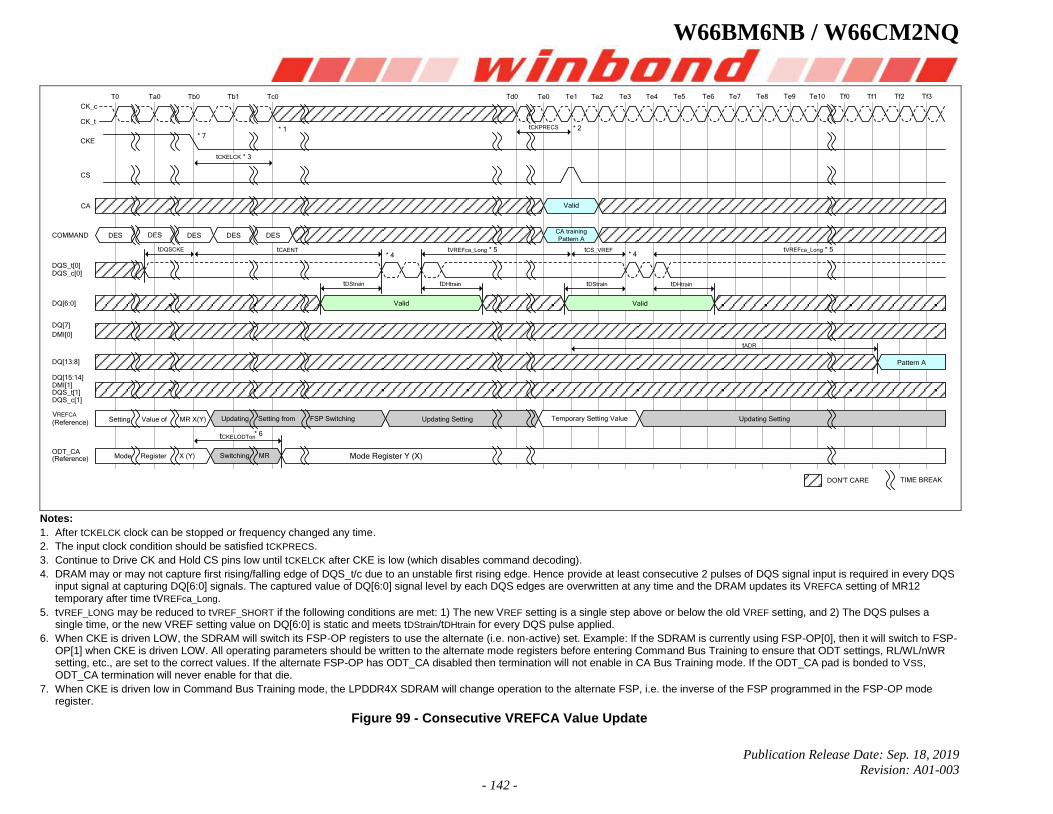
W66BM6NB / W66CM2NQ
Publication Release Date: Sep. 18, 2019
Revision: A01-003
- 142 -
T0 Ta0 Tb0 Tb1 Te2Tc0 Te3 Te4 Te5 Te6 Te7 Te8 Te9 Te10Td0 Tf0 Tf1 Tf2 Tf3
TIME BREAKDON'T CARE
Valid
DES DES DES DES DESCA training
Pattern A
Valid
Pattern A
CK_c
CK_t
CKE
CS
CA
COMMAND
DQS_t[0]DQS_c[0]
DQ[6:0]
DQ[7]
DMI[0]
DQ[13:8]
DQ[15:14]DMI[1]DQS_t[1]DQS_c[1]
VREFCA
(Reference)
ODT_CA(Reference) Switching MR
* 7* 1
tCKELCK * 3
* 2tCKPRECS
tADR
tVREFca_Long * 5tCAENT* 4
tDQSCKE
tCKELODTon* 6
Te0 Te1
tCS_VREF* 4
tVREFca_Long * 5
tDStrain tDHtraintDStrain tDHtrain
Valid
Setting Value of MR X(Y) Updating Setting from FSP Switching Updating Setting Temporary Setting Value Updating Setting
Mode Register X (Y) Mode Register Y (X)
Notes:
1. After tCKELCK clock can be stopped or frequency changed any time.
2. The input clock condition should be satisfied tCKPRECS.
3. Continue to Drive CK and Hold CS pins low until tCKELCK after CKE is low (which disables command decoding).
4. DRAM may or may not capture first rising/falling edge of DQS_t/c due to an unstable first rising edge. Hence provide at least consecutive 2 pulses of DQS signal input is required in every DQS input signal at capturing DQ[6:0] signals. The captured value of DQ[6:0] signal level by each DQS edges are overwritten at any time and the DRAM updates its VREFCA setting of MR12 temporary after time tVREFca_Long.
5. tVREF_LONG may be reduced to tVREF_SHORT if the following conditions are met: 1) The new VREF setting is a single step above or below the old VREF setting, and 2) The DQS pulses a single time, or the new VREF setting value on DQ[6:0] is static and meets tDStrain/tDHtrain for every DQS pulse applied.
6. When CKE is driven LOW, the SDRAM will switch its FSP-OP registers to use the alternate (i.e. non-active) set. Example: If the SDRAM is currently using FSP-OP[0], then it will switch to FSP-OP[1] when CKE is driven LOW. All operating parameters should be written to the alternate mode registers before entering Command Bus Training to ensure that ODT settings, RL/WL/nWR setting, etc., are set to the correct values. If the alternate FSP-OP has ODT_CA disabled then termination will not enable in CA Bus Training mode. If the ODT_CA pad is bonded to VSS, ODT_CA termination will never enable for that die.
7. When CKE is driven low in Command Bus Training mode, the LPDDR4X SDRAM will change operation to the alternate FSP, i.e. the inverse of the FSP programmed in the FSP-OP mode register.
Figure 99 - Consecutive VREFCA Value Update
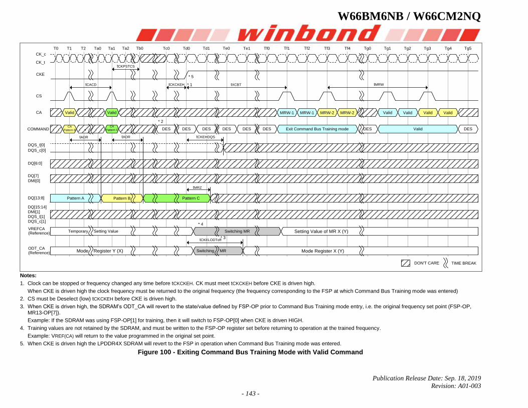
W66BM6NB / W66CM2NQ
Publication Release Date: Sep. 18, 2019
Revision: A01-003
- 143 -
Valid Valid MRW-1 MRW-1 MRW-2 MRW-2 Valid Valid Valid Valid
CA
Pattern B
CA
Pattern C DESDES DESDES DESDES DES DESValidExit Command Bus Training mode
Pattern A Pattern B Pattern C
Temporary Setting Value
Mode Register Y (X)
Switching MR
Switching MR
Setting Value of MR X (Y)
Mode Register X (Y)
tCACD
T0 T1 T2 Ta0 Ta1 Ta2 Tb0 Tc0 Td0 Td1 Te0 Te1 Tf0 Tf1 Tf2 Tf3 Tf4 Tg0 Tg1 Tg2 Tg3 Tg4 Tg5
CK_c
CK_t
CKE
CS
CA
COMMAND
DQS_t[0]
DQS_c[0]
DQ[6:0]
DQ[7]
DMI[0]
DQ[13:8]
DQ[15:14]DMI[1]DQS_t[1]DQS_c[1]
VREFCA(Reference)
ODT_CA(Reference)
TIME BREAKDON'T CARE
tCKPSTCS
tCKCKEH
* 5
tXCBT tMRW
* 2
tADR tADR tCKEHDQS
tMRZ
* 4
* 3tCKELODToff
* 1
Notes:
1. Clock can be stopped or frequency changed any time before tCKCKEH. CK must meet tCKCKEH before CKE is driven high.
When CKE is driven high the clock frequency must be returned to the original frequency (the frequency corresponding to the FSP at which Command Bus Training mode was entered)
2. CS must be Deselect (low) tCKCKEH before CKE is driven high.
3. When CKE is driven high, the SDRAM’s ODT_CA will revert to the state/value defined by FSP-OP prior to Command Bus Training mode entry, i.e. the original frequency set point (FSP-OP, MR13-OP[7]).
Example: If the SDRAM was using FSP-OP[1] for training, then it will switch to FSP-OP[0] when CKE is driven HIGH.
4. Training values are not retained by the SDRAM, and must be written to the FSP-OP register set before returning to operation at the trained frequency.
Example: VREF(CA) will return to the value programmed in the original set point.
5. When CKE is driven high the LPDDR4X SDRAM will revert to the FSP in operation when Command Bus Training mode was entered.
Figure 100 - Exiting Command Bus Training Mode with Valid Command
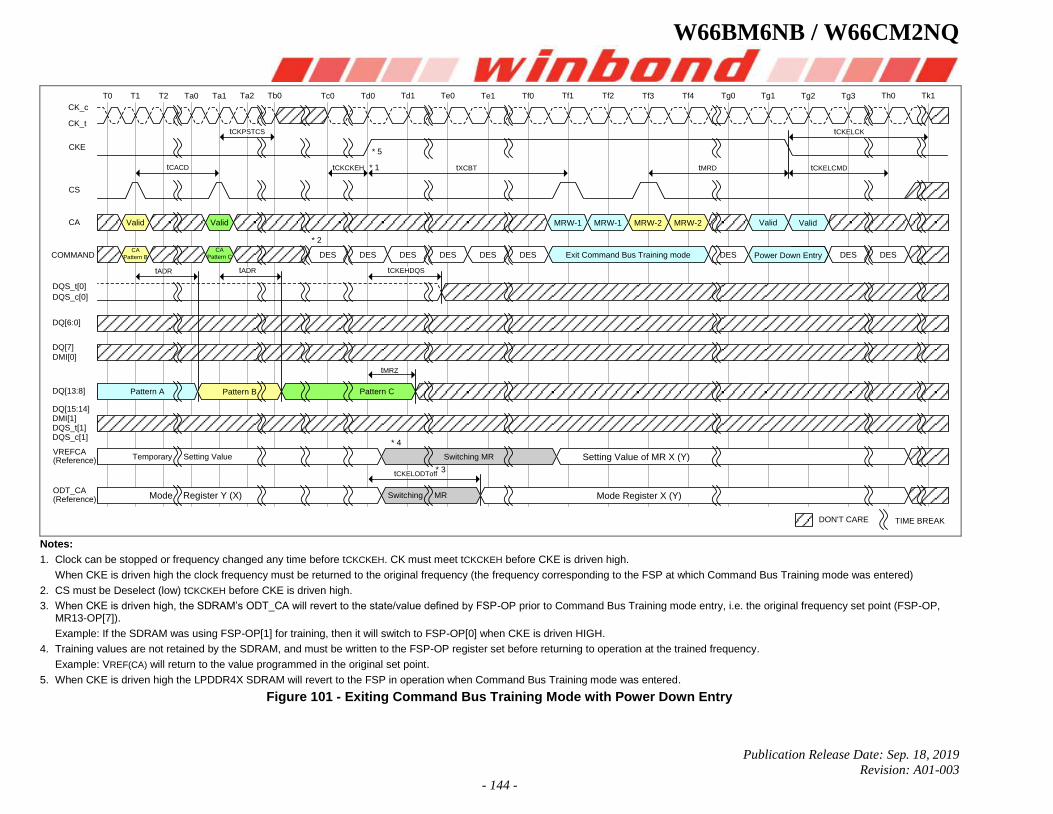
W66BM6NB / W66CM2NQ
Publication Release Date: Sep. 18, 2019
Revision: A01-003
- 144 -
Valid Valid MRW-1 MRW-1 MRW-2 MRW-2 Valid Valid
CA
Pattern B
CA
Pattern C DESDES DESDES DESDES DESExit Command Bus Training mode
Pattern A Pattern B Pattern C
Temporary Setting Value
Mode Register Y (X)
Switching MR
Switching MR
tCACD
T0 T1 T2 Ta0 Ta1 Ta2 Tb0 Tc0 Td0 Td1 Te0 Te1 Tf0 Tf1 Tf2 Tf3 Tf4 Tg0 Tg1 Tg2 Tg3 Th0 Tk1
CK_c
CK_t
CKE
CS
CA
COMMAND
DQS_t[0]
DQS_c[0]
DQ[6:0]
DQ[7]
DMI[0]
DQ[13:8]
DQ[15:14]DMI[1]DQS_t[1]DQS_c[1]
VREFCA(Reference)
ODT_CA(Reference)
TIME BREAKDON'T CARE
tCKPSTCS
tCKCKEH
* 5
tXCBT tMRD
* 2
tADR tADR tCKEHDQS
tMRZ
* 4
* 3tCKELODToff
* 1
Setting Value of MR X (Y)
Mode Register X (Y)
DES DESPower Down Entry
tCKELCK
tCKELCMD
Notes:
1. Clock can be stopped or frequency changed any time before tCKCKEH. CK must meet tCKCKEH before CKE is driven high.
When CKE is driven high the clock frequency must be returned to the original frequency (the frequency corresponding to the FSP at which Command Bus Training mode was entered)
2. CS must be Deselect (low) tCKCKEH before CKE is driven high.
3. When CKE is driven high, the SDRAM’s ODT_CA will revert to the state/value defined by FSP-OP prior to Command Bus Training mode entry, i.e. the original frequency set point (FSP-OP, MR13-OP[7]).
Example: If the SDRAM was using FSP-OP[1] for training, then it will switch to FSP-OP[0] when CKE is driven HIGH.
4. Training values are not retained by the SDRAM, and must be written to the FSP-OP register set before returning to operation at the trained frequency.
Example: VREF(CA) will return to the value programmed in the original set point.
5. When CKE is driven high the LPDDR4X SDRAM will revert to the FSP in operation when Command Bus Training mode was entered.
Figure 101 - Exiting Command Bus Training Mode with Power Down Entry
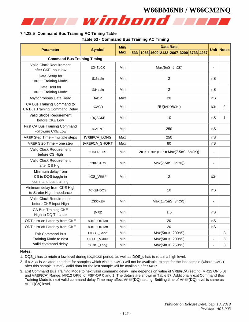
W66BM6NB / W66CM2NQ
Publication Release Date: Sep. 18, 2019
Revision: A01-003
- 145 -
7.4.28.5 Command Bus Training AC Timing Table
Table 53 - Command Bus Training AC Timing
Parameter Symbol Min/
Max
Data Rate Unit Notes
533 1066 1600 2133 2667 3200 3733 4267
Command Bus Training Timing
Valid Clock Requirement
after CKE Input low tCKELCK Min Max(5nS, 5nCK) -
Data Setup for
VREF Training Mode tDStrain Min 2 nS
Data Hold for
VREF Training Mode tDHtrain Min 2 nS
Asynchronous Data Read tADR Max 20 nS
CA Bus Training Command to
CA Bus Training Command Delay tCACD Min RU(tADR/tCK ) tCK 2
Valid Strobe Requirement
before CKE Low tDQSCKE Min 10 nS 1
First CA Bus Training Command
Following CKE Low tCAENT Min 250 nS
VREF Step Time – multiple steps tVREFCA_LONG Max 250 nS
VREF Step Time – one step tVREFCA_SHORT Max 80 nS
Valid Clock Requirement
before CS High tCKPRECS Min 2tCK + tXP (tXP = Max(7.5nS, 5nCK)) -
Valid Clock Requirement
after CS High tCKPSTCS Min Max(7.5nS, 5nCK)) -
Minimum delay from
CS to DQS toggle in
command bus training
tCS_VREF Min 2 tCK
Minimum delay from CKE High
to Strobe High Impedance tCKEHDQS 10 nS
Valid Clock Requirement
before CKE Input High tCKCKEH Min Max(1.75nS, 3nCK)) -
CA Bus Training CKE
High to DQ Tri-state tMRZ Min 1.5 nS
ODT turn-on Latency from CKE tCKELODTon Min 20 nS
ODT turn-off Latency from CKE tCKELODToff Min 20 nS
Exit Command Bus
Training Mode to next
valid command delay
tXCBT_Short Min Max(5nCK, 200nS) - 3
tXCBT_Middle Min Max(5nCK, 200nS) - 3
tXCBT_Long Min Max(5nCK, 250nS) - 3
Notes:
1. DQS_t has to retain a low level during tDQSCKE period, as well as DQS_c has to retain a high level.
2. If tCACD is violated, the data for samples which violate tCACD will not be available, except for the last sample (where tCACD after this sample is met). Valid data for the last sample will be available after tADR.
3. Exit Command Bus Training Mode to next valid command delay Time depends on value of VREF(CA) setting: MR12 OP[5:0] and VREF(CA) Range: MR12 OP[6] of FSP-OP 0 and 1. The details are shown in Table 57. Additionally exit Command Bus Training Mode to next valid command delay Time may affect VREF(DQ) setting. Settling time of VREF(DQ) level is same as VREF(CA) level.
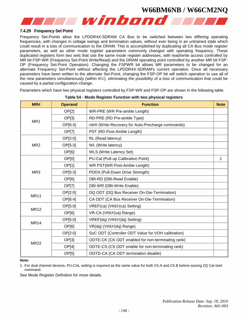
W66BM6NB / W66CM2NQ
Publication Release Date: Sep. 18, 2019
Revision: A01-003
- 146 -
7.4.29 Frequency Set Point
Frequency Set-Points allow the LPDDR4X-SDRAM CA Bus to be switched between two differing operating frequencies, with changes in voltage swings and termination values, without ever being in an untrained state which could result in a loss of communication to the DRAM. This is accomplished by duplicating all CA Bus mode register parameters, as well as other mode register parameters commonly changed with operating frequency. These duplicated registers form two sets that use the same mode register addresses, with read/write access controlled by MR bit FSP-WR (Frequency Set-Point Write/Read) and the DRAM operating point controlled by another MR bit FSP-OP (Frequency Set-Point Operation). Changing the FSPWR bit allows MR parameters to be changed for an alternate Frequency Set-Point without affecting the LPDDR4X-SDRAM's current operation. Once all necessary parameters have been written to the alternate Set-Point, changing the FSP-OP bit will switch operation to use all of the new parameters simultaneously (within tFC), eliminating the possibility of a loss of communication that could be caused by a partial configuration change.
Parameters which have two physical registers controlled by FSP-WR and FSP-OP are shown in the following table.
Table 54 - Mode Register Function with two physical registers
MR# Operand Function Note
MR1
OP[2] WR-PRE (WR Pre-amble Length)
OP[3] RD-PRE (RD Pre-amble Type)
OP[6:4] nWR (Write-Recovery for Auto-Precharge commands)
OP[7] PST (RD Post-Amble Length)
MR2
OP[2:0] RL (Read latency)
OP[5:3] WL (Write latency)
OP[6] WLS (Write Latency Set)
MR3
OP[0] PU-Cal (Pull-up Calibration Point) 1
OP[1] WR PST(WR Post-Amble Length)
OP[5:3] PDDS (Pull-Down Drive Strength)
OP[6] DBI-RD (DBI-Read Enable)
OP[7] DBI-WR (DBI-Write Enable)
MR11 OP[2:0] DQ ODT (DQ Bus Receiver On-Die-Termination)
OP[6:4] CA ODT (CA Bus Receiver On-Die-Termination)
MR12 OP[5:0] VREF(ca) (VREF(ca) Setting)
OP[6] VR-CA (VREF(ca) Range)
MR14 OP[5:0] VREF(dq) (VREF(dq) Setting)
OP[6] VR(dq) (VREF(dq) Range)
MR22
OP[2:0] SoC ODT (Controller ODT Value for VOH calibration)
OP[3] ODTE-CK (CK ODT enabled for non-terminating rank)
OP[4] ODTE-CS (CS ODT enable for non-terminating rank)
OP[5] ODTD-CA (CA ODT termination disable)
Note:
1. For dual channel devices, PU-CAL setting is required as the same value for both Ch.A and Ch.B before issuing ZQ Cal start command.
See Mode Register Definition for more details.
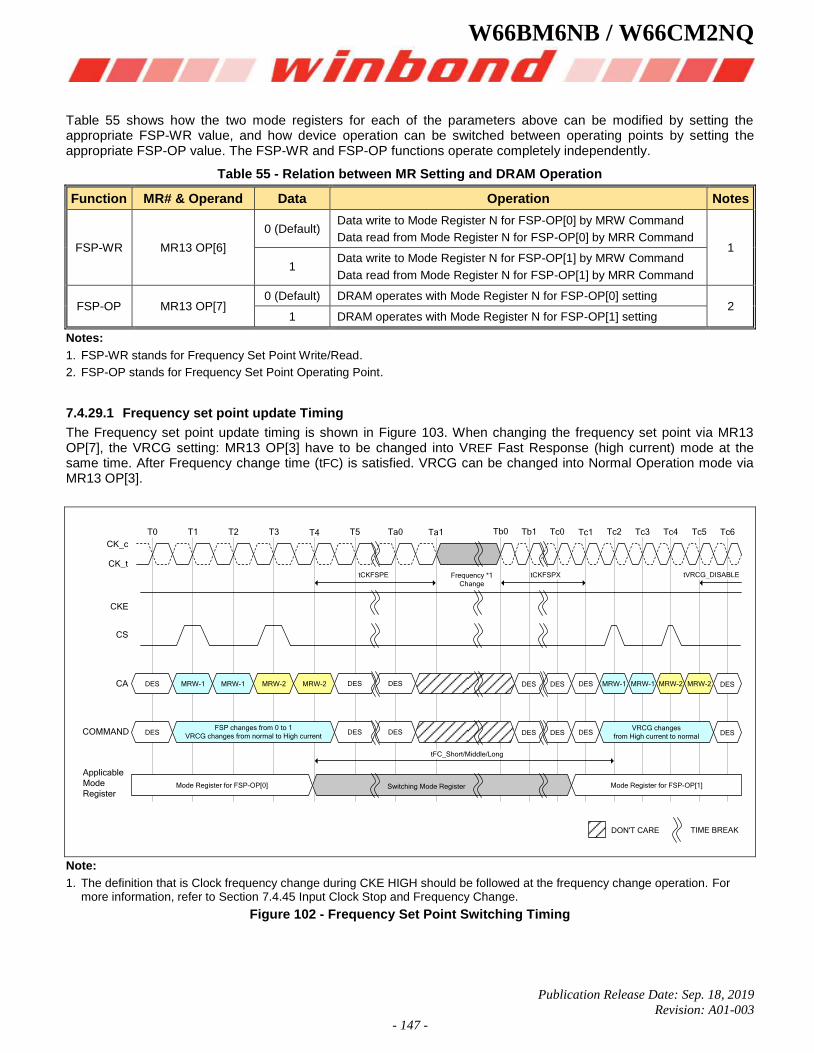
W66BM6NB / W66CM2NQ
Publication Release Date: Sep. 18, 2019
Revision: A01-003
- 147 -
Table 55 shows how the two mode registers for each of the parameters above can be modified by setting the appropriate FSP-WR value, and how device operation can be switched between operating points by setting the appropriate FSP-OP value. The FSP-WR and FSP-OP functions operate completely independently.
Table 55 - Relation between MR Setting and DRAM Operation
Function MR# & Operand Data Operation Notes
FSP-WR MR13 OP[6]
0 (Default) Data write to Mode Register N for FSP-OP[0] by MRW Command
Data read from Mode Register N for FSP-OP[0] by MRR Command 1
1 Data write to Mode Register N for FSP-OP[1] by MRW Command
Data read from Mode Register N for FSP-OP[1] by MRR Command
FSP-OP MR13 OP[7] 0 (Default) DRAM operates with Mode Register N for FSP-OP[0] setting
2 1 DRAM operates with Mode Register N for FSP-OP[1] setting
Notes:
1. FSP-WR stands for Frequency Set Point Write/Read.
2. FSP-OP stands for Frequency Set Point Operating Point.
7.4.29.1 Frequency set point update Timing
The Frequency set point update timing is shown in Figure 103. When changing the frequency set point via MR13 OP[7], the VRCG setting: MR13 OP[3] have to be changed into VREF Fast Response (high current) mode at the same time. After Frequency change time (tFC) is satisfied. VRCG can be changed into Normal Operation mode via MR13 OP[3].
T0 T1 T2 T3 T4 T5 Ta0 Ta1 Tb0 Tb1 Tc0 Tc1 Tc2 Tc3 Tc4 Tc5 Tc6
COMMAND
Applicable
Mode
Register
TIME BREAKDON'T CARE
DES DES DES DES DES DES DESMRW-1 MRW-1 MRW-2 MRW-2 MRW-1 MRW-1 MRW-2 MRW-2
DES DES DES DES DES DES DESVRCG changes
from High current to normal
FSP changes from 0 to 1
VRCG changes from normal to High current
Mode Register for FSP-OP[0] Switching Mode Register Mode Register for FSP-OP[1]
CK_c
CK_t
CS
CA
CKE
tCKFSPXtCKFSPE tVRCG_DISABLEFrequency *1
Change
tFC_Short/Middle/Long
Note:
1. The definition that is Clock frequency change during CKE HIGH should be followed at the frequency change operation. For more information, refer to Section 7.4.45 Input Clock Stop and Frequency Change.
Figure 102 - Frequency Set Point Switching Timing
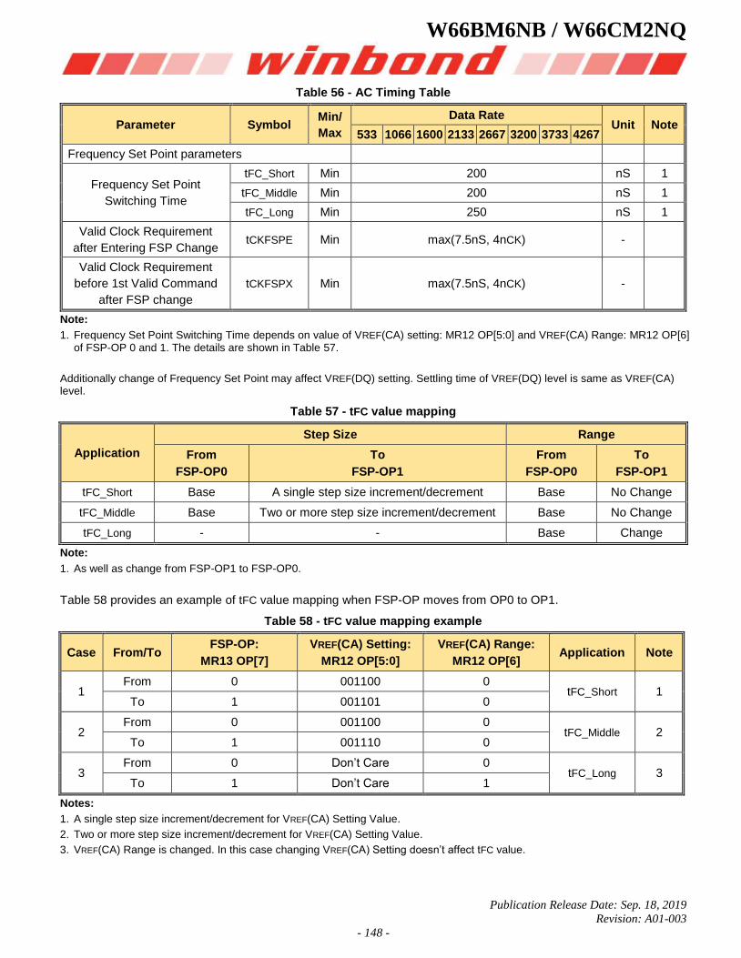
W66BM6NB / W66CM2NQ
Publication Release Date: Sep. 18, 2019
Revision: A01-003
- 148 -
Table 56 - AC Timing Table
Parameter Symbol Min/
Max
Data Rate Unit Note
533 1066 1600 2133 2667 3200 3733 4267
Frequency Set Point parameters
Frequency Set Point
Switching Time
tFC_Short Min 200 nS 1
tFC_Middle Min 200 nS 1
tFC_Long Min 250 nS 1
Valid Clock Requirement
after Entering FSP Change tCKFSPE Min max(7.5nS, 4nCK) -
Valid Clock Requirement
before 1st Valid Command
after FSP change
tCKFSPX Min max(7.5nS, 4nCK) -
Note:
1. Frequency Set Point Switching Time depends on value of VREF(CA) setting: MR12 OP[5:0] and VREF(CA) Range: MR12 OP[6] of FSP-OP 0 and 1. The details are shown in Table 57.
Additionally change of Frequency Set Point may affect VREF(DQ) setting. Settling time of VREF(DQ) level is same as VREF(CA) level.
Table 57 - tFC value mapping
Application
Step Size Range
From
FSP-OP0
To
FSP-OP1
From
FSP-OP0
To
FSP-OP1
tFC_Short Base A single step size increment/decrement Base No Change
tFC_Middle Base Two or more step size increment/decrement Base No Change
tFC_Long - - Base Change
Note:
1. As well as change from FSP-OP1 to FSP-OP0.
Table 58 provides an example of tFC value mapping when FSP-OP moves from OP0 to OP1.
Table 58 - tFC value mapping example
Case From/To FSP-OP:
MR13 OP[7]
VREF(CA) Setting:
MR12 OP[5:0]
VREF(CA) Range:
MR12 OP[6] Application Note
1 From 0 001100 0
tFC_Short 1 To 1 001101 0
2 From 0 001100 0
tFC_Middle 2 To 1 001110 0
3 From 0 Don’t Care 0
tFC_Long 3 To 1 Don’t Care 1
Notes:
1. A single step size increment/decrement for VREF(CA) Setting Value.
2. Two or more step size increment/decrement for VREF(CA) Setting Value.
3. VREF(CA) Range is changed. In this case changing VREF(CA) Setting doesn’t affect tFC value.
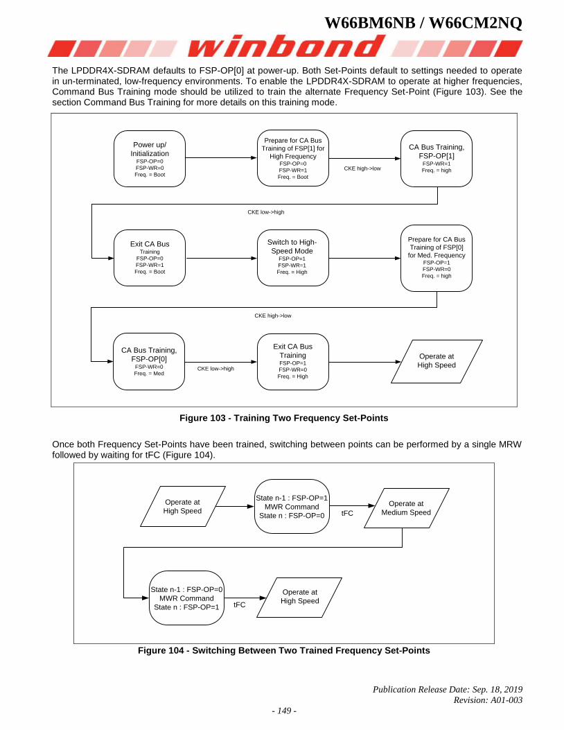
W66BM6NB / W66CM2NQ
Publication Release Date: Sep. 18, 2019
Revision: A01-003
- 149 -
The LPDDR4X-SDRAM defaults to FSP-OP[0] at power-up. Both Set-Points default to settings needed to operate in un-terminated, low-frequency environments. To enable the LPDDR4X-SDRAM to operate at higher frequencies, Command Bus Training mode should be utilized to train the alternate Frequency Set-Point (Figure 103). See the section Command Bus Training for more details on this training mode.
Power up/
InitializationFSP-OP=0
FSP-WR=0
Freq. = Boot
Exit CA BusTraining
FSP-OP=0
FSP-WR=1
Freq. = Boot
CA Bus Training,
FSP-OP[0]FSP-WR=0
Freq. = Med
Exit CA Bus
TrainingFSP-OP=1
FSP-WR=0
Freq. = High
Switch to High-
Speed ModeFSP-OP=1
FSP-WR=1
Freq. = High
Prepare for CA Bus
Training of FSP[1] for
High FrequencyFSP-OP=0
FSP-WR=1
Freq. = Boot
CA Bus Training,
FSP-OP[1]FSP-WR=1
Freq. = high
Prepare for CA Bus
Training of FSP[0]
for Med. FrequencyFSP-OP=1
FSP-WR=0
Freq. = high
Operate at
High SpeedCKE low->high
CKE high->low
CKE low->high
CKE high->low
Figure 103 - Training Two Frequency Set-Points
Once both Frequency Set-Points have been trained, switching between points can be performed by a single MRW followed by waiting for tFC (Figure 104).
Operate at
High Speed
State n-1 : FSP-OP=1
MWR Command
State n : FSP-OP=0 tFC
tFC
Operate at
Medium Speed
State n-1 : FSP-OP=0
MWR Command
State n : FSP-OP=1
Operate at
High Speed
Figure 104 - Switching Between Two Trained Frequency Set-Points
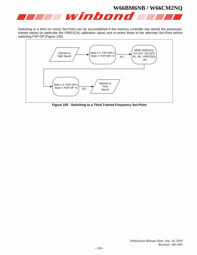
W66BM6NB / W66CM2NQ
Publication Release Date: Sep. 18, 2019
Revision: A01-003
- 150 -
Switching to a third (or more) Set-Point can be accomplished if the memory controller has stored the previously-trained values (in particular the VREF(CA) calibration value) and re-writes these to the alternate Set-Point before switching FSP-OP (Figure 105).
Operate at
High Speed
Operate at
Third
Speed
State n-1: FSP-WR=1
State n: FSP-WR =0
MRW VREF(CA),
CA-ODT, DQ-ODT,
RL, WL, VREF(DQ),
...etc.
State n-1: FSP-OP=1
State n: FSP-OP =0
tFC
tFC
Figure 105 - Switching to a Third Trained Frequency Set-Point
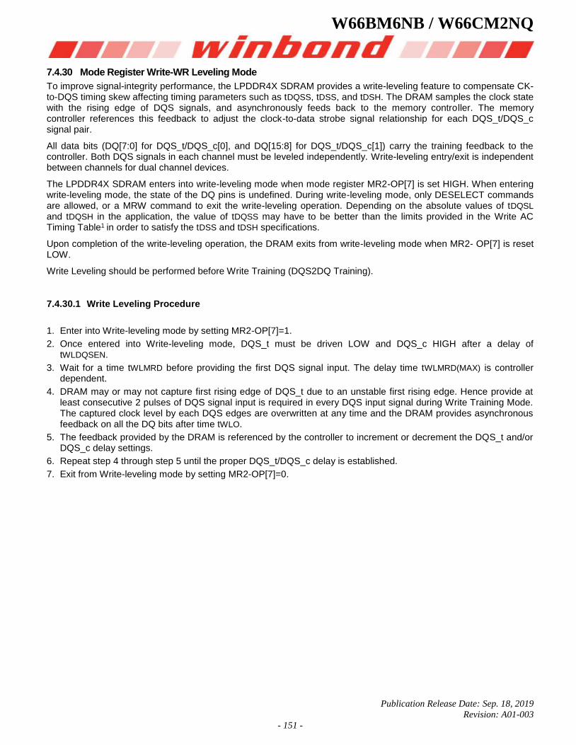
W66BM6NB / W66CM2NQ
Publication Release Date: Sep. 18, 2019
Revision: A01-003
- 151 -
7.4.30 Mode Register Write-WR Leveling Mode
To improve signal-integrity performance, the LPDDR4X SDRAM provides a write-leveling feature to compensate CK-to-DQS timing skew affecting timing parameters such as tDQSS, tDSS, and tDSH. The DRAM samples the clock state with the rising edge of DQS signals, and asynchronously feeds back to the memory controller. The memory controller references this feedback to adjust the clock-to-data strobe signal relationship for each DQS_t/DQS_c signal pair.
All data bits (DQ[7:0] for DQS_t/DQS_c[0], and DQ[15:8] for DQS_t/DQS_c[1]) carry the training feedback to the controller. Both DQS signals in each channel must be leveled independently. Write-leveling entry/exit is independent between channels for dual channel devices.
The LPDDR4X SDRAM enters into write-leveling mode when mode register MR2-OP[7] is set HIGH. When entering write-leveling mode, the state of the DQ pins is undefined. During write-leveling mode, only DESELECT commands are allowed, or a MRW command to exit the write-leveling operation. Depending on the absolute values of tDQSL and tDQSH in the application, the value of tDQSS may have to be better than the limits provided in the Write AC Timing Table1 in order to satisfy the tDSS and tDSH specifications.
Upon completion of the write-leveling operation, the DRAM exits from write-leveling mode when MR2- OP[7] is reset LOW.
Write Leveling should be performed before Write Training (DQS2DQ Training).
7.4.30.1 Write Leveling Procedure
1. Enter into Write-leveling mode by setting MR2-OP[7]=1.
2. Once entered into Write-leveling mode, DQS_t must be driven LOW and DQS_c HIGH after a delay of tWLDQSEN.
3. Wait for a time tWLMRD before providing the first DQS signal input. The delay time tWLMRD(MAX) is controller dependent.
4. DRAM may or may not capture first rising edge of DQS_t due to an unstable first rising edge. Hence provide at least consecutive 2 pulses of DQS signal input is required in every DQS input signal during Write Training Mode. The captured clock level by each DQS edges are overwritten at any time and the DRAM provides asynchronous feedback on all the DQ bits after time tWLO.
5. The feedback provided by the DRAM is referenced by the controller to increment or decrement the DQS_t and/or DQS_c delay settings.
6. Repeat step 4 through step 5 until the proper DQS_t/DQS_c delay is established.
7. Exit from Write-leveling mode by setting MR2-OP[7]=0.
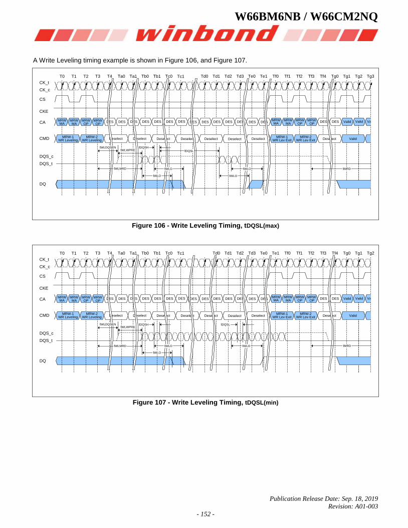
W66BM6NB / W66CM2NQ
Publication Release Date: Sep. 18, 2019
Revision: A01-003
- 152 -
A Write Leveling timing example is shown in Figure 106, and Figure 107.
T0 T1 T2 T3 T4 Tb0 Tb1 Tc1Ta0 Ta1 Tc0 Tf0 Tf1Te0 Tf2 Tg0 Tg1Tf3 Tf4 Tg2
CMD
tWLWPREtDQSH
CK_t
CK_c
CKE
CS
CA
DQS_c
DQS_t
DQ
MRWMA
MRWMA
MRWOP
MRWOP
WR LevelingMRW-2
WR LevelingMRW-1
DES DES DES DES DES DES DES DES DES DES DES Valid Valid
Deselect Deselect Deselect Deselect Deselect
Te1
tWLDQSEN
Td0 Td1 Td2 Td3
DES DES DES DES DESMRWMA
MRWMA
MRWOP
MRWOP
Va
Deselect Deselect Deselect WR Lev ExitMRW-2
WR Lev ExitMRW-1
Valid
tMRD
Tg3
tWLO
tWLOtWLO
tWLOtWLMRD
tDQSL
Figure 106 - Write Leveling Timing, tDQSL(max)
T0 T1 T2 T3 T4 Tb0 Tb1 Tc1Ta0 Ta1 Tc0 Tf0 Tf1Te0 Tf2 Tg0 Tg1Tf3 Tf4 Tg2
CMD
tWLWPREtDQSH tDQSL
CK_t
CK_c
CKE
CS
CA
DQS_c
DQS_t
DQ
MRWMA
MRWMA
MRWOP
MRWOP
WR LevelingMRW-2
WR LevelingMRW-1
DES DES DES DES DES DES DES DES DES DES DES Valid Valid
Deselect Deselect Deselect Deselect Deselect
Te1
tWLDQSEN
Td0 Td1 Td2 Td3
DES DES DES DES DESMRWMA
MRWMA
MRWOP
MRWOP
Va
Deselect Deselect Deselect WR Lev ExitMRW-2
WR Lev ExitMRW-1
Valid
tWLO
tWLO
tWLMRD tWLO tMRD
Figure 107 - Write Leveling Timing, tDQSL(min)
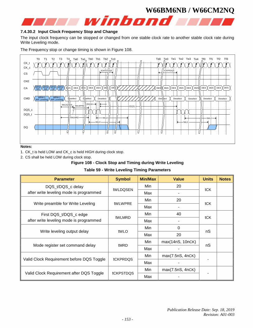
W66BM6NB / W66CM2NQ
Publication Release Date: Sep. 18, 2019
Revision: A01-003
- 153 -
7.4.30.2 Input Clock Frequency Stop and Change
The input clock frequency can be stopped or changed from one stable clock rate to another stable clock rate during Write Leveling mode.
The Frequency stop or change timing is shown in Figure 108.
T0 T1 T2 T3 T4 Tb0 Tb1 Tc0Ta0 Ta1 Tb2 Te1 Te2Td0 Te3 Tf1 Tf2Te4 Tf0 Tf3
CMD
tWLMRD
tWLWPREtDQSH
tWLO
tWLO
tDQSL
tWLO
tWLO
tCKPRDQS
CK_t
CK_c
CKE
CS
CA
DQS_c
DQS_t
DQ
MRWMA
MRWMA
MRWOP
MRWOP
WR LevelingMRW-2
WR LevelingMRW-1
DES DES DES DES DES DES DES DES DES DES DES DES DES DES DES DES DES
Deselect Deselect Deselect Deselect Deselect Deselect Deselect Deselect
Te0
tWLDQSEN
tCKPSTDQS
Notes:
1. CK_t is held LOW and CK_c is held HIGH during clock stop.
2. CS shall be held LOW during clock stop.
Figure 108 - Clock Stop and Timing during Write Leveling
Table 59 - Write Leveling Timing Parameters
Parameter Symbol Min/Max Value Units Notes
DQS_t/DQS_c delay
after write leveling mode is programmed tWLDQSEN
Min 20 tCK
Max -
Write preamble for Write Leveling tWLWPRE Min 20
tCK Max -
First DQS_t/DQS_c edge
after write leveling mode is programmed tWLMRD
Min 40 tCK
Max -
Write leveling output delay tWLO Min 0
nS Max 20
Mode register set command delay tMRD Min max(14nS, 10nCK)
nS Max -
Valid Clock Requirement before DQS Toggle tCKPRDQS Min max(7.5nS, 4nCK)
- Max -
Valid Clock Requirement after DQS Toggle tCKPSTDQS Min max(7.5nS, 4nCK)
- Max -
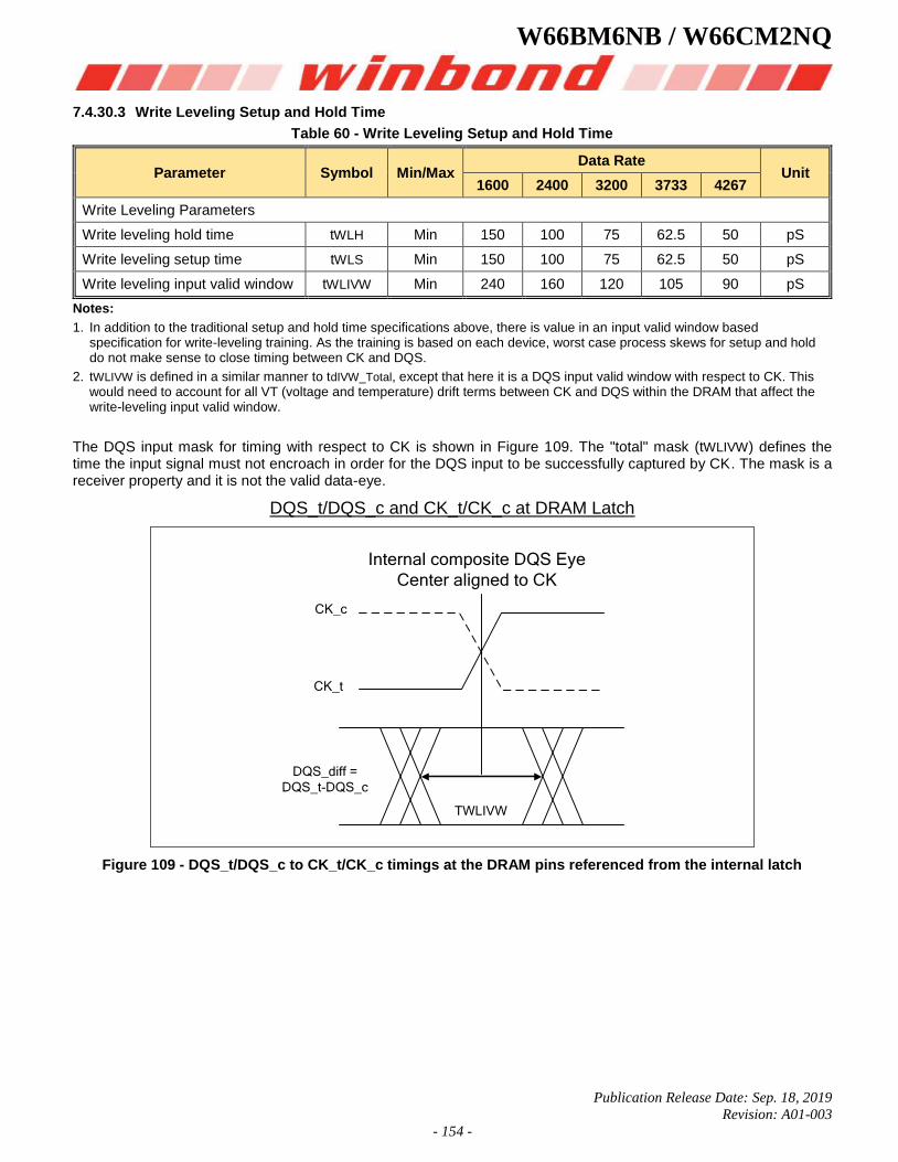
W66BM6NB / W66CM2NQ
Publication Release Date: Sep. 18, 2019
Revision: A01-003
- 154 -
7.4.30.3 Write Leveling Setup and Hold Time
Table 60 - Write Leveling Setup and Hold Time
Parameter Symbol Min/Max Data Rate
Unit 1600 2400 3200 3733 4267
Write Leveling Parameters
Write leveling hold time tWLH Min 150 100 75 62.5 50 pS
Write leveling setup time tWLS Min 150 100 75 62.5 50 pS
Write leveling input valid window tWLIVW Min 240 160 120 105 90 pS
Notes:
1. In addition to the traditional setup and hold time specifications above, there is value in an input valid window based specification for write-leveling training. As the training is based on each device, worst case process skews for setup and hold do not make sense to close timing between CK and DQS.
2. tWLIVW is defined in a similar manner to tdIVW_Total, except that here it is a DQS input valid window with respect to CK. This would need to account for all VT (voltage and temperature) drift terms between CK and DQS within the DRAM that affect the write-leveling input valid window.
The DQS input mask for timing with respect to CK is shown in Figure 109. The "total" mask (tWLIVW) defines the time the input signal must not encroach in order for the DQS input to be successfully captured by CK. The mask is a receiver property and it is not the valid data-eye.
DQS_t/DQS_c and CK_t/CK_c at DRAM Latch
DQS_diff =
DQS_t-DQS_c
CK_c
CK_t
Internal composite DQS Eye
Center aligned to CK
TWLIVW
Figure 109 - DQS_t/DQS_c to CK_t/CK_c timings at the DRAM pins referenced from the internal latch
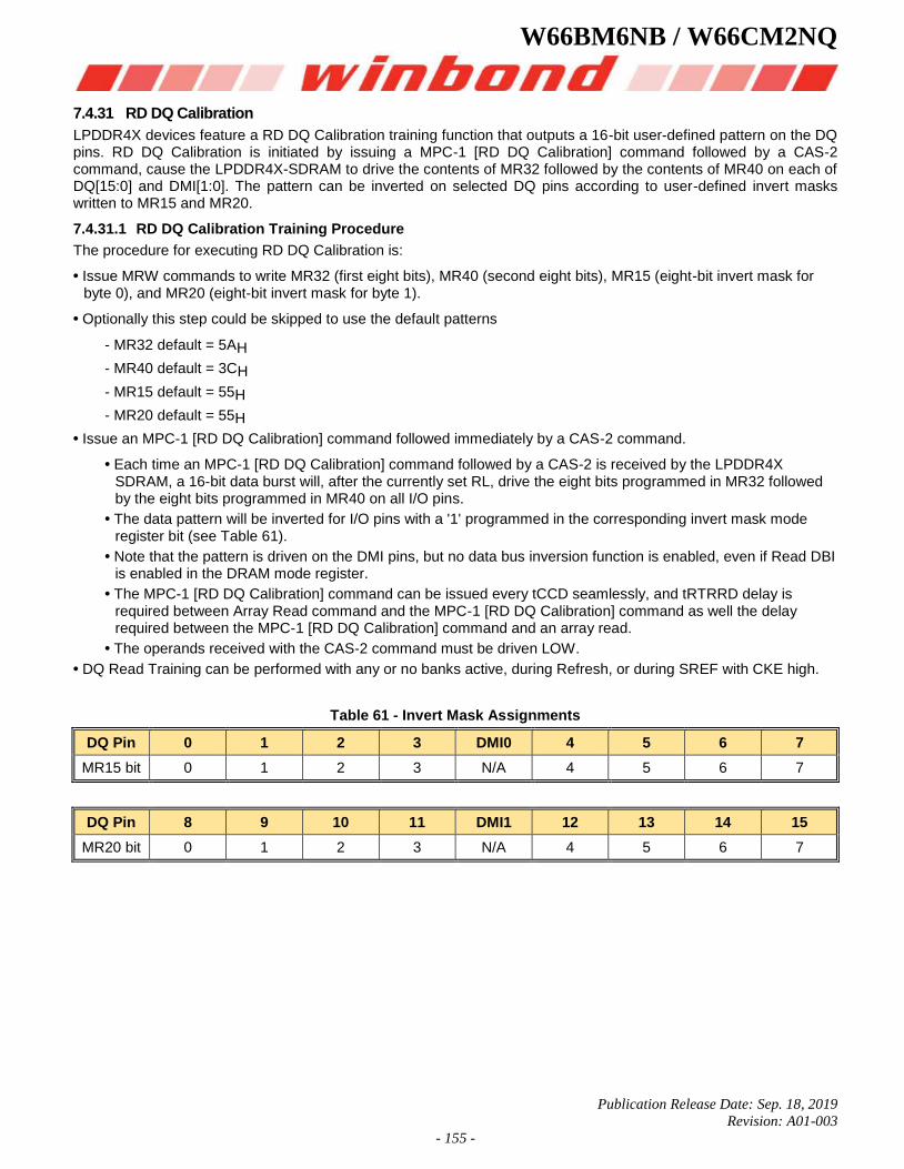
W66BM6NB / W66CM2NQ
Publication Release Date: Sep. 18, 2019
Revision: A01-003
- 155 -
7.4.31 RD DQ Calibration
LPDDR4X devices feature a RD DQ Calibration training function that outputs a 16-bit user-defined pattern on the DQ pins. RD DQ Calibration is initiated by issuing a MPC-1 [RD DQ Calibration] command followed by a CAS-2 command, cause the LPDDR4X-SDRAM to drive the contents of MR32 followed by the contents of MR40 on each of DQ[15:0] and DMI[1:0]. The pattern can be inverted on selected DQ pins according to user-defined invert masks written to MR15 and MR20.
7.4.31.1 RD DQ Calibration Training Procedure
The procedure for executing RD DQ Calibration is:
• Issue MRW commands to write MR32 (first eight bits), MR40 (second eight bits), MR15 (eight-bit invert mask for byte 0), and MR20 (eight-bit invert mask for byte 1).
• Optionally this step could be skipped to use the default patterns
- MR32 default = 5AH
- MR40 default = 3CH
- MR15 default = 55H
- MR20 default = 55H
• Issue an MPC-1 [RD DQ Calibration] command followed immediately by a CAS-2 command.
• Each time an MPC-1 [RD DQ Calibration] command followed by a CAS-2 is received by the LPDDR4X SDRAM, a 16-bit data burst will, after the currently set RL, drive the eight bits programmed in MR32 followed by the eight bits programmed in MR40 on all I/O pins.
• The data pattern will be inverted for I/O pins with a '1' programmed in the corresponding invert mask mode register bit (see Table 61).
• Note that the pattern is driven on the DMI pins, but no data bus inversion function is enabled, even if Read DBI is enabled in the DRAM mode register.
• The MPC-1 [RD DQ Calibration] command can be issued every tCCD seamlessly, and tRTRRD delay is required between Array Read command and the MPC-1 [RD DQ Calibration] command as well the delay required between the MPC-1 [RD DQ Calibration] command and an array read.
• The operands received with the CAS-2 command must be driven LOW.
• DQ Read Training can be performed with any or no banks active, during Refresh, or during SREF with CKE high.
Table 61 - Invert Mask Assignments
DQ Pin 0 1 2 3 DMI0 4 5 6 7
MR15 bit 0 1 2 3 N/A 4 5 6 7
DQ Pin 8 9 10 11 DMI1 12 13 14 15
MR20 bit 0 1 2 3 N/A 4 5 6 7
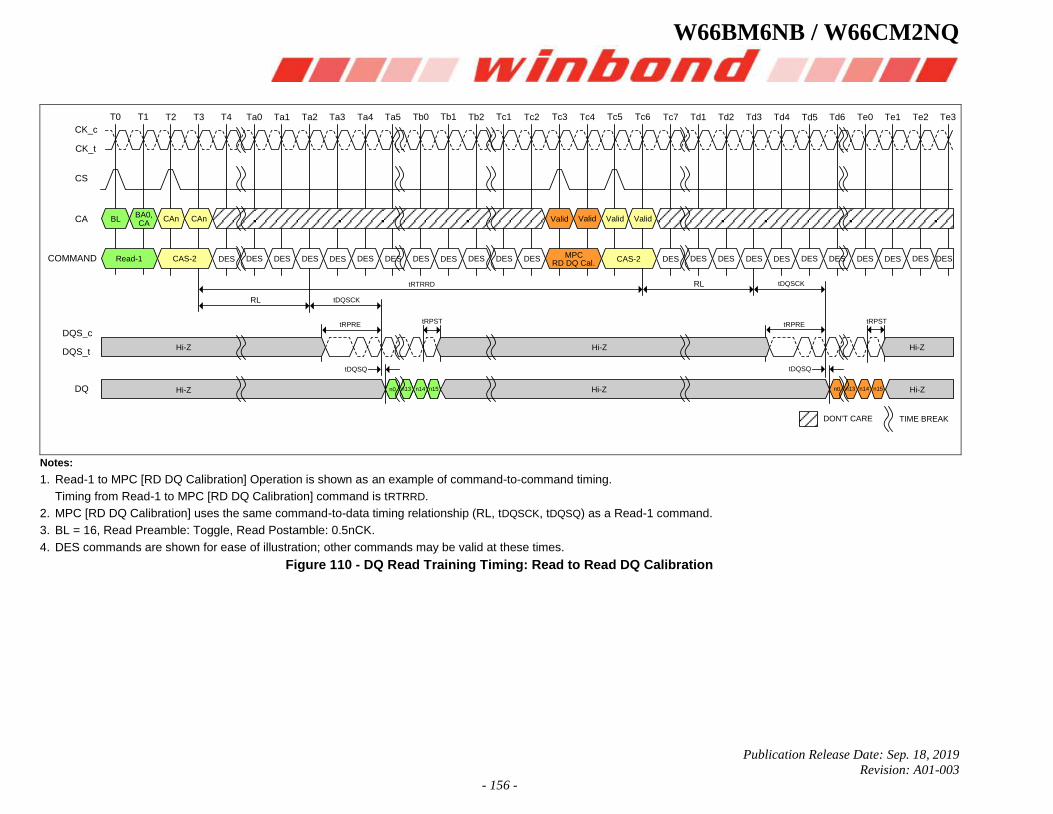
W66BM6NB / W66CM2NQ
Publication Release Date: Sep. 18, 2019
Revision: A01-003
- 156 -
BLBA0,CA
CAn CAn Valid Valid ValidValid
DES DES DESDES DES DES DESDES DES DES DESDES DES DES DESDES DES DES DESDES DES DESRead-1 CAS-2 CAS-2MPC
RD DQ Cal.DES
Hi-Z Hi-Z Hi-Z
Hi-ZHi-ZHi-Z
TIME BREAKDON'T CARE
T0 T1 T2 T3 T4 Ta0 Ta1 Ta2 Ta3 Ta4 Ta5 Tb0 Tb1 Tb2 Tc1 Tc2 Tc3 Tc4 Tc5 Tc6 Tc7 Td1 Td2 Td3 Td4 Td5 Td6 Te0 Te1 Te2 Te3
CK_c
CK_t
CA
COMMAND
CS
DQ
DQS_c
DQS_t
n0 n13 n14 n15 n0 n13 n14 n15
tRPRE
tDQSQ
tRPST
tDQSCK
tRTRRD
tRPRE
tDQSQ
tRPST
RL
RL tDQSCK
Notes:
1. Read-1 to MPC [RD DQ Calibration] Operation is shown as an example of command-to-command timing.
Timing from Read-1 to MPC [RD DQ Calibration] command is tRTRRD.
2. MPC [RD DQ Calibration] uses the same command-to-data timing relationship (RL, tDQSCK, tDQSQ) as a Read-1 command.
3. BL = 16, Read Preamble: Toggle, Read Postamble: 0.5nCK.
4. DES commands are shown for ease of illustration; other commands may be valid at these times.
Figure 110 - DQ Read Training Timing: Read to Read DQ Calibration
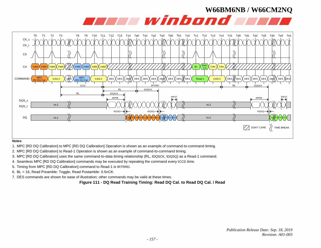
W66BM6NB / W66CM2NQ
Publication Release Date: Sep. 18, 2019
Revision: A01-003
- 157 -
BLBA0,CA
CAn CAnValid Valid ValidValid Valid ValidValid Valid
DES DESDES DES DES DESDES DES DES DES DESDES DES DESRead-1 CAS-2CAS-2MPC
RD DQ Cal.DES
T0 T1 T2 T3 T8 T9 T10 T11 T12 T13 Ta0 Ta1 Ta2 Ta3 Tb0 Tb1 Tc0 Tc1 Tc2 Tc3 Tc4 Tc5 Td0 Td1 Td2 Td3 Td4 Te0 Te1T14
CK_c
CK_t
CA
COMMAND
CS
DQ
DQS_c
DQS_t
n0 n13 n14 n15
tRPRE
tDQSQ
tRPST
tDQSCK
tRTRRD
tRPRE
tDQSQ
tRPST
RL
RL tDQSCK
CAS-2MPC
RD DQ Cal.DES DES DESDES
n0 n13 n14 n15n12 n13 n14 n15n0 n9 n10 n11
Hi-Z
Hi-Z
tDQSQ
tDQSCK
tCCD
RL
Hi-Z
Hi-Z
TIME BREAKDON'T CARE
Notes:
1. MPC [RD DQ Calibration] to MPC [RD DQ Calibration] Operation is shown as an example of command-to-command timing.
2. MPC [RD DQ Calibration] to Read-1 Operation is shown as an example of command-to-command timing.
3. MPC [RD DQ Calibration] uses the same command-to-data timing relationship (RL, tDQSCK, tDQSQ) as a Read-1 command.
4. Seamless MPC [RD DQ Calibration] commands may be executed by repeating the command every tCCD time.
5. Timing from MPC [RD DQ Calibration] command to Read-1 is tRTRRD.
6. BL = 16, Read Preamble: Toggle, Read Postamble: 0.5nCK.
7. DES commands are shown for ease of illustration; other commands may be valid at these times.
Figure 111 - DQ Read Training Timing: Read DQ Cal. to Read DQ Cal. / Read
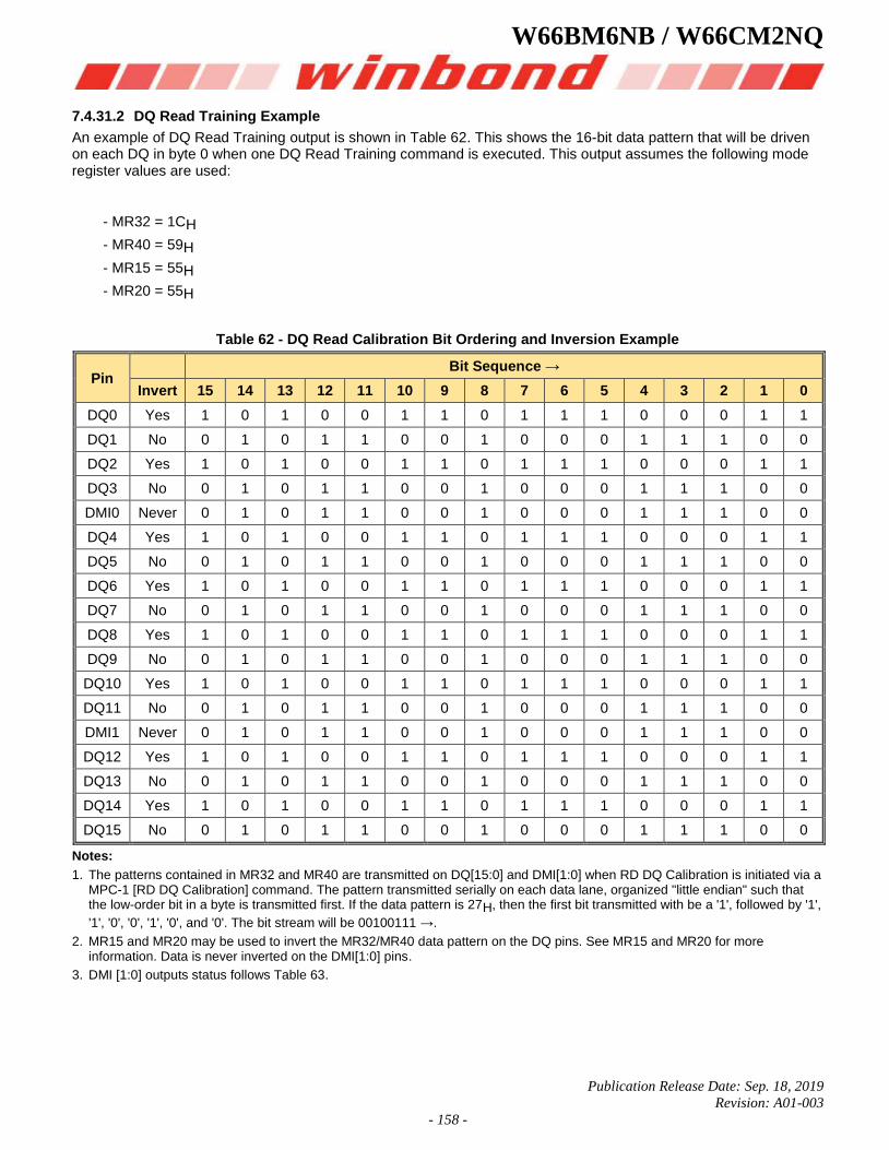
W66BM6NB / W66CM2NQ
Publication Release Date: Sep. 18, 2019
Revision: A01-003
- 158 -
7.4.31.2 DQ Read Training Example
An example of DQ Read Training output is shown in Table 62. This shows the 16-bit data pattern that will be driven on each DQ in byte 0 when one DQ Read Training command is executed. This output assumes the following mode register values are used:
- MR32 = 1CH
- MR40 = 59H
- MR15 = 55H
- MR20 = 55H
Table 62 - DQ Read Calibration Bit Ordering and Inversion Example
Pin Bit Sequence →
Invert 15 14 13 12 11 10 9 8 7 6 5 4 3 2 1 0
DQ0 Yes 1 0 1 0 0 1 1 0 1 1 1 0 0 0 1 1
DQ1 No 0 1 0 1 1 0 0 1 0 0 0 1 1 1 0 0
DQ2 Yes 1 0 1 0 0 1 1 0 1 1 1 0 0 0 1 1
DQ3 No 0 1 0 1 1 0 0 1 0 0 0 1 1 1 0 0
DMI0 Never 0 1 0 1 1 0 0 1 0 0 0 1 1 1 0 0
DQ4 Yes 1 0 1 0 0 1 1 0 1 1 1 0 0 0 1 1
DQ5 No 0 1 0 1 1 0 0 1 0 0 0 1 1 1 0 0
DQ6 Yes 1 0 1 0 0 1 1 0 1 1 1 0 0 0 1 1
DQ7 No 0 1 0 1 1 0 0 1 0 0 0 1 1 1 0 0
DQ8 Yes 1 0 1 0 0 1 1 0 1 1 1 0 0 0 1 1
DQ9 No 0 1 0 1 1 0 0 1 0 0 0 1 1 1 0 0
DQ10 Yes 1 0 1 0 0 1 1 0 1 1 1 0 0 0 1 1
DQ11 No 0 1 0 1 1 0 0 1 0 0 0 1 1 1 0 0
DMI1 Never 0 1 0 1 1 0 0 1 0 0 0 1 1 1 0 0
DQ12 Yes 1 0 1 0 0 1 1 0 1 1 1 0 0 0 1 1
DQ13 No 0 1 0 1 1 0 0 1 0 0 0 1 1 1 0 0
DQ14 Yes 1 0 1 0 0 1 1 0 1 1 1 0 0 0 1 1
DQ15 No 0 1 0 1 1 0 0 1 0 0 0 1 1 1 0 0
Notes:
1. The patterns contained in MR32 and MR40 are transmitted on DQ[15:0] and DMI[1:0] when RD DQ Calibration is initiated via a MPC-1 [RD DQ Calibration] command. The pattern transmitted serially on each data lane, organized "little endian" such that the low-order bit in a byte is transmitted first. If the data pattern is 27H, then the first bit transmitted with be a '1', followed by '1',
'1', '0', '0', '1', '0', and '0'. The bit stream will be 00100111 →.
2. MR15 and MR20 may be used to invert the MR32/MR40 data pattern on the DQ pins. See MR15 and MR20 for more information. Data is never inverted on the DMI[1:0] pins.
3. DMI [1:0] outputs status follows Table 63.
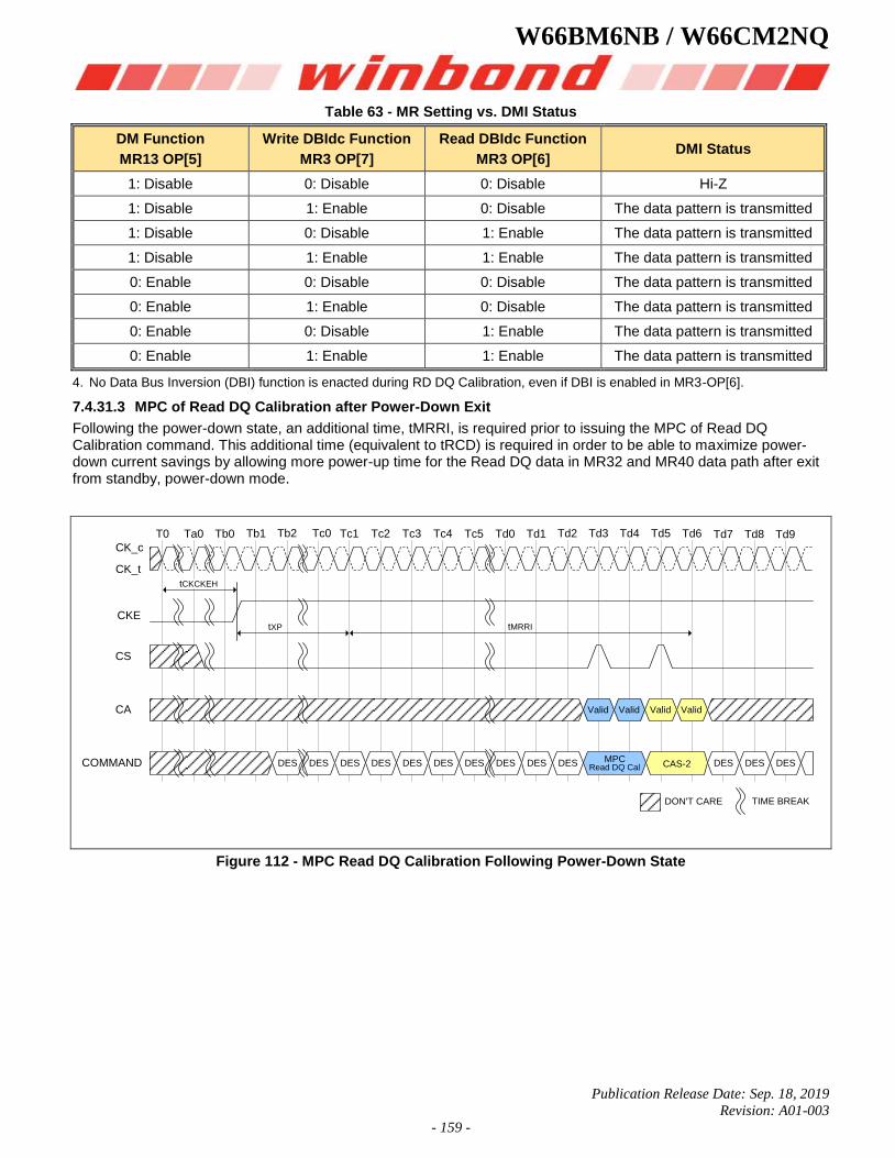
W66BM6NB / W66CM2NQ
Publication Release Date: Sep. 18, 2019
Revision: A01-003
- 159 -
Table 63 - MR Setting vs. DMI Status
DM Function
MR13 OP[5]
Write DBIdc Function
MR3 OP[7]
Read DBIdc Function
MR3 OP[6] DMI Status
1: Disable 0: Disable 0: Disable Hi-Z
1: Disable 1: Enable 0: Disable The data pattern is transmitted
1: Disable 0: Disable 1: Enable The data pattern is transmitted
1: Disable 1: Enable 1: Enable The data pattern is transmitted
0: Enable 0: Disable 0: Disable The data pattern is transmitted
0: Enable 1: Enable 0: Disable The data pattern is transmitted
0: Enable 0: Disable 1: Enable The data pattern is transmitted
0: Enable 1: Enable 1: Enable The data pattern is transmitted
4. No Data Bus Inversion (DBI) function is enacted during RD DQ Calibration, even if DBI is enabled in MR3-OP[6].
7.4.31.3 MPC of Read DQ Calibration after Power-Down Exit
Following the power-down state, an additional time, tMRRI, is required prior to issuing the MPC of Read DQ Calibration command. This additional time (equivalent to tRCD) is required in order to be able to maximize power-down current savings by allowing more power-up time for the Read DQ data in MR32 and MR40 data path after exit from standby, power-down mode.
Valid Valid Valid Valid
DES DESDES DES DES DESDES
T0 Ta0 Tb0 Tb1 Tb2 Tc0 Tc1 Tc2 Tc3 Tc4 Tc5 Td0 Td1 Td2 Td3 Td4 Td5 Td6 Td7 Td8 Td9CK_c
CK_t
COMMAND
CA
CS
CKE
TIME BREAKDON'T CARE
tXP tMRRI
DES DES MPCCAS-2
tCKCKEH
DES DES DES DES Read DQ Cal
Figure 112 - MPC Read DQ Calibration Following Power-Down State
W66BM6NB / W66CM2NQ
Publication Release Date: Sep. 18, 2019
Revision: A01-003
- 160 -
7.4.32 DQS-DQ Training
The LPDDR4X-SDRAM uses an un-matched DQS-DQ path to enable high speed performance and save power in the DRAM. As a result, the DQS strobe must be trained to arrive at the DQ latch center-aligned with the Data eye. The SDRAM DQ receiver is located at the DQ pad, and has a shorter internal delay in the SDRAM than does the DQS signal. The SDRAM DQ receiver will latch the data present on the DQ bus when DQS reaches the latch, and training is accomplished by delaying the DQ signals relative to DQS such that the Data eye arrives at the receiver latch centered on the DQS transition.
Two modes of training are available in LPDDR4X:
• Command-based FIFO WR/RD with user patterns
• An internal DQS clock-tree oscillator, to determine the need for, and the magnitude of required training.
The command-based FIFO WR/RD uses the MPC command with operands to enable this special mode of operation. When issuing the MPC command, if OP6 is set LOW then the DRAM will perform a NOP command. When OP6 is set HIGH, then OP5:0 enable training functions or are reserved for future use (RFU). MPC commands that initiate a Read FIFO, READ DQ Calibration or Write FIFO to the SDRAM must be followed immediately by a CAS-2 command. See "Multi-Purpose Command (MPC) Definition" for more information.
To perform Write Training, the controller can issue a MPC [Write DQ FIFO] command with OP[6:0] set as described in the MPC Definition section, followed immediately by a CAS-2 command (CAS-2 operands should be driven LOW) to initiate a Write DQ FIFO. Timings for MPC [Write DQ FIFO] are identical to a Write command, with WL (Write Latency) timed from the 2nd rising clock edge of the CAS-2 command. Up to 5 consecutive MPC [Write DQ FIFO] commands with user defined patterns may be issued to the SDRAM to store up to 80 values (BL16 x5) per pin that can be read back via the MPC [Read DQ FIFO] command. Write/Read FIFO Pointer operation is described later in this section.
After writing data to the SDRAM with the MPC [Write DQ FIFO] command, the data can be read back with the MPC [Read DQ FIFO] command and results compared with “expect” data to see if further training (DQ delay) is needed. MPC [Read DQ FIFO] is initiated by issuing a MPC command with OP[6:0] set as described in the MPC Definition section, followed immediately by a CAS-2 command (CAS-2 operands must be driven LOW). Timings for the MPC [Read DQ FIFO] command are identical to a Read command, with RL (Read Latency) timed from the 2nd rising clock edge of the CAS-2 command.
Read DQ FIFO is non-destructive to the data captured in the FIFO, so data may be read continuously until it is either overwritten by a Write DQ FIFO command or disturbed by CKE LOW or any of the following commands; Write, Masked Write, Read, Read DQ Calibration and a MRR. If fewer than 5 Write DQ FIFO commands were executed, then unwritten registers will have un-defined (but valid) data when read back.
For example: If 5 Write DQ FIFO commands are executed sequentially, then a series of Read DQ FIFO commands will read valid data from FIFO[0], FIFO[1]….FIFO[4], and will then wrap back to FIFO[0] on the next Read DQ FIFO.
On the other hand, if fewer than 5 Write DQ FIFO commands are executed sequentially (example=3), then a series of Read DQ FIFO commands will return valid data for FIFO[0], FIFO[1], and FIFO[2], but the next two Read DQ FIFO commands will return un-defined data for FIFO[3] and FIFO[4] before wrapping back to the valid data in FIFO[0].
W66BM6NB / W66CM2NQ
Publication Release Date: Sep. 18, 2019
Revision: A01-003
- 161 -
7.4.32.1 FIFO Pointer Reset and Synchronism
The Read and Write DQ FIFO pointers are reset under the following conditions:
• Power-up initialization
• RESET_n asserted
• Power-down entry
• Self Refresh Power-Down entry
The MPC [Write DQ FIFO] command advances the WR-FIFO pointer, and the MPC [Read DQ FIFO] advances the RD-FIFO pointer. Also any normal (non-FIFO) Read Operation (RD, RDA) advances both WR-FIFO pointer and RD-FIFO pointer. Issuing (non-FIFO) Read Operation command is inhibited during Write training period. To keep the pointers aligned, the SoC memory controller must adhere to the following restriction at the end of Write training period:
• b = a + (n x c)
Where:
‘a’ is the number of MPC [Write DQ FIFO] commands
‘b’ is the number of MPC [Read DQ FIFO] commands
‘c’ is the FIFO depth (=5 for LPDDR4X)
‘n’ is a positive integer, ≥0
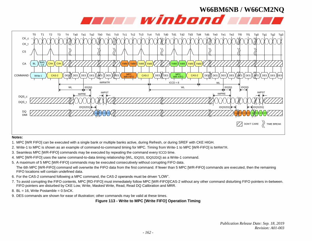
W66BM6NB / W66CM2NQ
Publication Release Date: Sep. 18, 2019
Revision: A01-003
- 162 -
DES DESDES DES DES DESDES DES DES DES DESDES DES DESCAS-2CAS-2 DES
T0 T1 T2 T3 Ta0 Ta1 Ta2 Tb0 Tb1 Tc0 Tc2 Tc3 Tc4 Tc5 Td0 Td1 Td2 Td3 Td4 Td5 Te0 Te1 Te2 Tf0 Tf1 Tg0 Tg1 Tg2 Tg3Tc1
CK_c
CK_t
CA
COMMAND
CS
DQ
DQS_c
DQS_t
tWPREtWPST
tWRWTR
WL tDQSS
CAS-2MPC
WR FIFODESDES DESDES
tCCD = 8
WL
T4
Valid Valid Valid Valid ValidValid Valid
MPCWR FIFO
DMI
tDQSS
tDQS2DQ
n0 n13 n14 n15
BLBA0,CA
CAn CAn
Write-1
Valid
WL
n0 n13 n14 n15
tWPRE
n0 n13 n14 n15
tWPST
tDQS2DQ
tDQSS
tDQS2DQ
TIME BREAKDON'T CARE
Notes:
1. MPC [WR FIFO] can be executed with a single bank or multiple banks active, during Refresh, or during SREF with CKE HIGH.
2. Write-1 to MPC is shown as an example of command-to-command timing for MPC. Timing from Write-1 to MPC [WR-FIFO] is tWRWTR.
3. Seamless MPC [WR-FIFO] commands may be executed by repeating the command every tCCD time.
4. MPC [WR-FIFO] uses the same command-to-data timing relationship (WL, tDQSS, tDQS2DQ) as a Write-1 command.
5. A maximum of 5 MPC [WR-FIFO] commands may be executed consecutively without corrupting FIFO data.
The 6th MPC [WR-FIFO] command will overwrite the FIFO data from the first command. If fewer than 5 MPC [WR-FIFO] commands are executed, then the remaining FIFO locations will contain undefined data.
6. For the CAS-2 command following a MPC command, the CAS-2 operands must be driven “LOW”.
7. To avoid corrupting the FIFO contents, MPC [RD-FIFO] must immediately follow MPC [WR-FIFO]/CAS-2 without any other command disturbing FIFO pointers in-between. FIFO pointers are disturbed by CKE Low, Write, Masked Write, Read, Read DQ Calibration and MRR.
8. BL = 16, Write Postamble = 0.5nCK.
9. DES commands are shown for ease of illustration; other commands may be valid at these times.
Figure 113 - Write to MPC [Write FIFO] Operation Timing
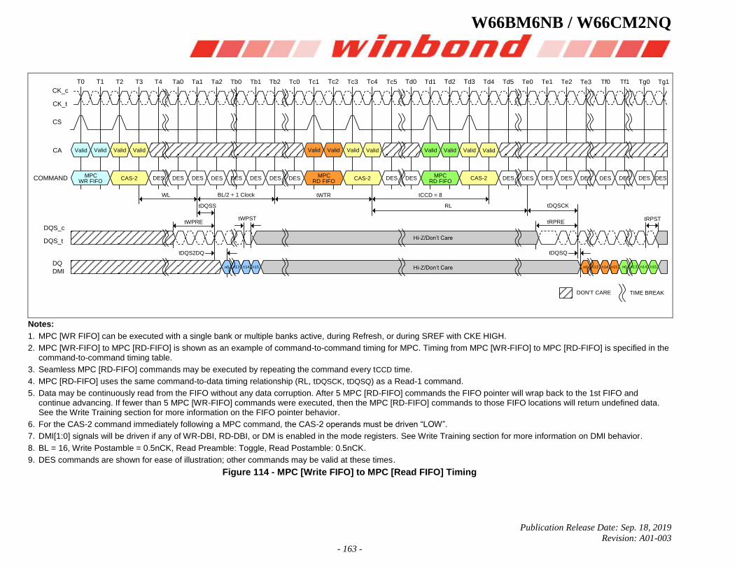
W66BM6NB / W66CM2NQ
Publication Release Date: Sep. 18, 2019
Revision: A01-003
- 163 -
Valid Valid ValidValid
DES DESDES DES DES DESDES DES DES DES DESDES DES DESCAS-2CAS-2MPC
WR FIFODES
T0 T1 T2 T3 Ta0 Ta1 Ta2 Tb0 Tb1 Tb2 Tc1 Tc2 Tc3 Tc4 Tc5 Td0 Td1 Td2 Td3 Td4 Td5 Te0 Te1 Te2 Te3 Tf0 Tf1 Tg0 Tg1Tc0
CK_c
CK_t
CA
COMMAND
CS
DQ
DQS_c
DQS_t
n0 n13 n14 n15
tWPREtWPST
tWTR
tRPRE
tDQSQ
tRPST
RL tDQSCK
CAS-2MPC
RD FIFODES DES DESDES
n0 n13 n14 n15
tCCD = 8WL
T4
Valid ValidValid Valid Valid ValidValid Valid
MPCRD FIFO
BL/2 + 1 Clock
DMI
tDQSS
Hi-Z/Don’t Care
tDQS2DQ
n0 n13 n14 n15 Hi-Z/Don’t Care
TIME BREAKDON'T CARE
Notes:
1. MPC [WR FIFO] can be executed with a single bank or multiple banks active, during Refresh, or during SREF with CKE HIGH.
2. MPC [WR-FIFO] to MPC [RD-FIFO] is shown as an example of command-to-command timing for MPC. Timing from MPC [WR-FIFO] to MPC [RD-FIFO] is specified in the command-to-command timing table.
3. Seamless MPC [RD-FIFO] commands may be executed by repeating the command every tCCD time.
4. MPC [RD-FIFO] uses the same command-to-data timing relationship (RL, tDQSCK, tDQSQ) as a Read-1 command.
5. Data may be continuously read from the FIFO without any data corruption. After 5 MPC [RD-FIFO] commands the FIFO pointer will wrap back to the 1st FIFO and continue advancing. If fewer than 5 MPC [WR-FIFO] commands were executed, then the MPC [RD-FIFO] commands to those FIFO locations will return undefined data. See the Write Training section for more information on the FIFO pointer behavior.
6. For the CAS-2 command immediately following a MPC command, the CAS-2 operands must be driven “LOW”.
7. DMI[1:0] signals will be driven if any of WR-DBI, RD-DBI, or DM is enabled in the mode registers. See Write Training section for more information on DMI behavior.
8. BL = 16, Write Postamble = 0.5nCK, Read Preamble: Toggle, Read Postamble: 0.5nCK.
9. DES commands are shown for ease of illustration; other commands may be valid at these times.
Figure 114 - MPC [Write FIFO] to MPC [Read FIFO] Timing
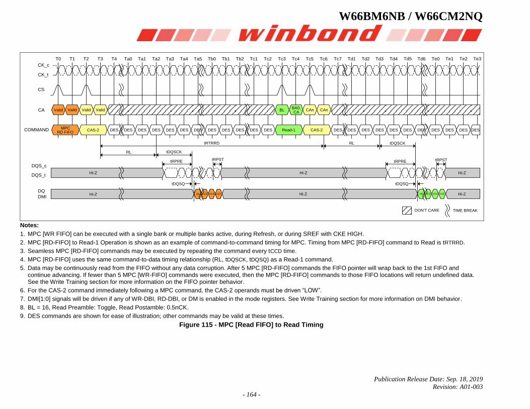
W66BM6NB / W66CM2NQ
Publication Release Date: Sep. 18, 2019
Revision: A01-003
- 164 -
BLBA0,CA
CAn CAnValid Valid ValidValid
DES DESDES DES DES DESDES DES DES DES DESDES DES DESRead-1 CAS-2CAS-2MPC
RD FIFODES
T0 T1 T2 T3 Ta0 Ta1 Ta2 Ta3 Ta4 Ta5 Tb1 Tb2 Tc1 Tc2 Tc3 Tc4 Tc5 Tc6 Tc7 Td1 Td2 Td3 Td4 Td5 Td6 Te0 Te1 Te2 Te3Tb0
CK_c
CK_t
CA
COMMAND
CS
DQS_c
DQS_t
n0 n13 n14 n15
tRPRE
tDQSQ
tRPST
tDQSCK
tRTRRD
tRPRE
tDQSQ
tRPST
RL
RL tDQSCK
DES DES DESDES
n0 n13 n14 n15
T4
DQ
DMI
DES DES DES DES
Hi-Z
Hi-Z
Hi-Z
Hi-Z
Hi-Z
Hi-Z
TIME BREAKDON'T CARE
Notes:
1. MPC [WR FIFO] can be executed with a single bank or multiple banks active, during Refresh, or during SREF with CKE HIGH.
2. MPC [RD-FIFO] to Read-1 Operation is shown as an example of command-to-command timing for MPC. Timing from MPC [RD-FIFO] command to Read is tRTRRD.
3. Seamless MPC [RD-FIFO] commands may be executed by repeating the command every tCCD time.
4. MPC [RD-FIFO] uses the same command-to-data timing relationship (RL, tDQSCK, tDQSQ) as a Read-1 command.
5. Data may be continuously read from the FIFO without any data corruption. After 5 MPC [RD-FIFO] commands the FIFO pointer will wrap back to the 1st FIFO and continue advancing. If fewer than 5 MPC [WR-FIFO] commands were executed, then the MPC [RD-FIFO] commands to those FIFO locations will return undefined data. See the Write Training section for more information on the FIFO pointer behavior.
6. For the CAS-2 command immediately following a MPC command, the CAS-2 operands must be driven “LOW”.
7. DMI[1:0] signals will be driven if any of WR-DBI, RD-DBI, or DM is enabled in the mode registers. See Write Training section for more information on DMI behavior.
8. BL = 16, Read Preamble: Toggle, Read Postamble: 0.5nCK.
9. DES commands are shown for ease of illustration; other commands may be valid at these times.
Figure 115 - MPC [Read FIFO] to Read Timing
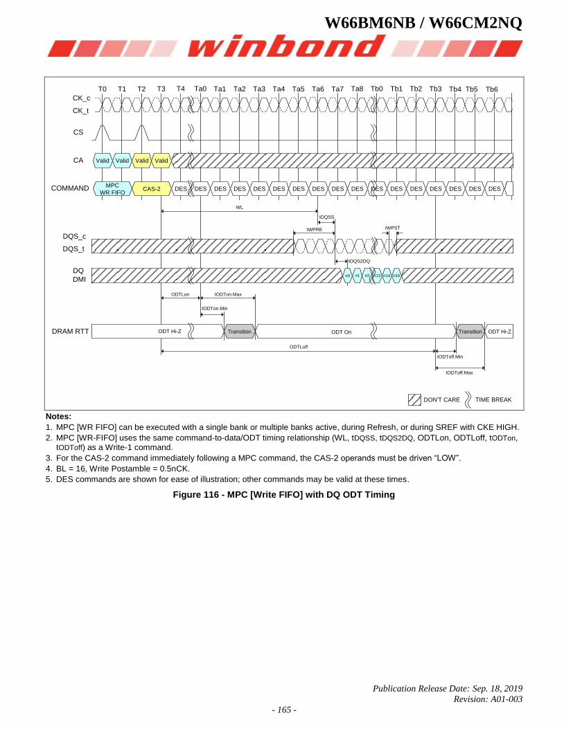
W66BM6NB / W66CM2NQ
Publication Release Date: Sep. 18, 2019
Revision: A01-003
- 165 -
T0 T1 T2 T3 T4 Ta0 Ta1 Ta2 Ta3 Ta4 Ta5 Ta6 Ta7 Ta8 Tb0 Tb1 Tb2 Tb3 Tb4 Tb5 Tb6
Valid Valid Valid Valid
MPC
WR FIFOCAS-2 DES DES DES DES DES DES DES DES DES DES DES DES DES DES DES DES DES
n0 n13 n14 n15n1 n2
TIME BREAKDON'T CARE
tDQSS
tWPRE tWPST
WL
tDQS2DQ
ODTLon tODTon.Max
tODTon.Min
ODTLoff
tODToff.Max
tODToff.Min
CK_c
CK_t
COMMAND
CA
CS
DQS_c
DQS_t
DQ
DMI
Transition TransitionODT Hi-Z ODT Hi-ZODT OnDRAM RTT
Notes:
1. MPC [WR FIFO] can be executed with a single bank or multiple banks active, during Refresh, or during SREF with CKE HIGH.
2. MPC [WR-FIFO] uses the same command-to-data/ODT timing relationship (WL, tDQSS, tDQS2DQ, ODTLon, ODTLoff, tODTon, tODToff) as a Write-1 command.
3. For the CAS-2 command immediately following a MPC command, the CAS-2 operands must be driven “LOW”.
4. BL = 16, Write Postamble = 0.5nCK.
5. DES commands are shown for ease of illustration; other commands may be valid at these times.
Figure 116 - MPC [Write FIFO] with DQ ODT Timing
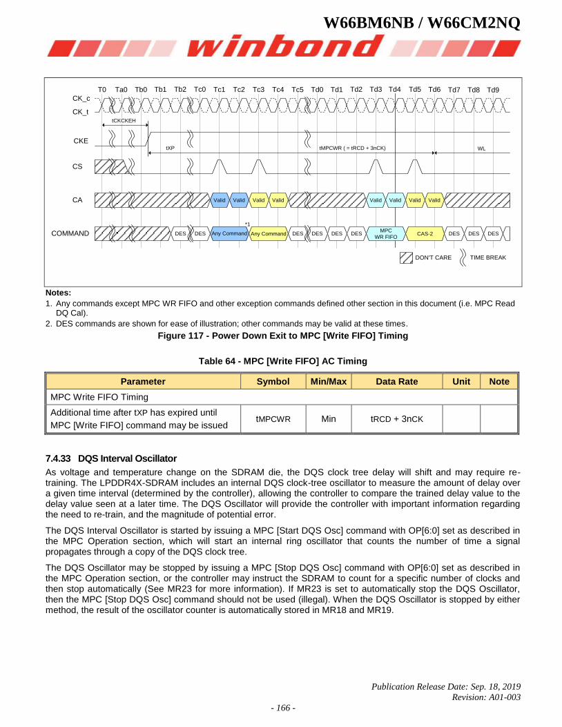
W66BM6NB / W66CM2NQ
Publication Release Date: Sep. 18, 2019
Revision: A01-003
- 166 -
Valid Valid Valid Valid Valid Valid Valid Valid
DES DES DES DES DES DESAny CommandMPC
WR FIFOCAS-2
T0 Ta0 Tb0 Tb1 Tb2 Tc0 Tc1 Tc2 Tc3 Tc4 Tc5 Td0 Td1 Td2 Td3 Td4 Td5 Td6 Td7 Td8 Td9CK_c
CK_t
COMMAND
CA
CS
CKE
TIME BREAKDON'T CARE
Any Command DES DES DES
tCKCKEH
tXP WLtMPCWR ( = tRCD + 3nCK)
*1
Notes:
1. Any commands except MPC WR FIFO and other exception commands defined other section in this document (i.e. MPC Read DQ Cal).
2. DES commands are shown for ease of illustration; other commands may be valid at these times.
Figure 117 - Power Down Exit to MPC [Write FIFO] Timing
Table 64 - MPC [Write FIFO] AC Timing
Parameter Symbol Min/Max Data Rate Unit Note
MPC Write FIFO Timing
Additional time after tXP has expired until
MPC [Write FIFO] command may be issued tMPCWR Min tRCD + 3nCK
7.4.33 DQS Interval Oscillator
As voltage and temperature change on the SDRAM die, the DQS clock tree delay will shift and may require re-training. The LPDDR4X-SDRAM includes an internal DQS clock-tree oscillator to measure the amount of delay over a given time interval (determined by the controller), allowing the controller to compare the trained delay value to the delay value seen at a later time. The DQS Oscillator will provide the controller with important information regarding the need to re-train, and the magnitude of potential error.
The DQS Interval Oscillator is started by issuing a MPC [Start DQS Osc] command with OP[6:0] set as described in the MPC Operation section, which will start an internal ring oscillator that counts the number of time a signal propagates through a copy of the DQS clock tree.
The DQS Oscillator may be stopped by issuing a MPC [Stop DQS Osc] command with OP[6:0] set as described in the MPC Operation section, or the controller may instruct the SDRAM to count for a specific number of clocks and then stop automatically (See MR23 for more information). If MR23 is set to automatically stop the DQS Oscillator, then the MPC [Stop DQS Osc] command should not be used (illegal). When the DQS Oscillator is stopped by either method, the result of the oscillator counter is automatically stored in MR18 and MR19.
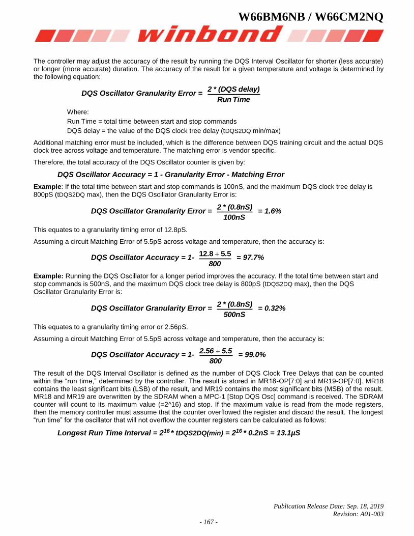
W66BM6NB / W66CM2NQ
Publication Release Date: Sep. 18, 2019
Revision: A01-003
- 167 -
The controller may adjust the accuracy of the result by running the DQS Interval Oscillator for shorter (less accurate) or longer (more accurate) duration. The accuracy of the result for a given temperature and voltage is determined by the following equation:
DQS Oscillator Granularity Error = Time Run
delay)(DQS * 2
Where:
Run Time = total time between start and stop commands
DQS delay = the value of the DQS clock tree delay (tDQS2DQ min/max)
Additional matching error must be included, which is the difference between DQS training circuit and the actual DQS clock tree across voltage and temperature. The matching error is vendor specific.
Therefore, the total accuracy of the DQS Oscillator counter is given by:
DQS Oscillator Accuracy = 1 - Granularity Error - Matching Error
Example: If the total time between start and stop commands is 100nS, and the maximum DQS clock tree delay is 800pS (tDQS2DQ max), then the DQS Oscillator Granularity Error is:
DQS Oscillator Granularity Error = 100nS
(0.8nS) * 2 = 1.6%
This equates to a granularity timing error of 12.8pS.
Assuming a circuit Matching Error of 5.5pS across voltage and temperature, then the accuracy is:
DQS Oscillator Accuracy = 1- 800
5.5 12.8 = 97.7%
Example: Running the DQS Oscillator for a longer period improves the accuracy. If the total time between start and stop commands is 500nS, and the maximum DQS clock tree delay is 800pS (tDQS2DQ max), then the DQS Oscillator Granularity Error is:
DQS Oscillator Granularity Error = 500nS
(0.8nS) * 2 = 0.32%
This equates to a granularity timing error or 2.56pS.
Assuming a circuit Matching Error of 5.5pS across voltage and temperature, then the accuracy is:
DQS Oscillator Accuracy = 1- 800
5.5 2.56 = 99.0%
The result of the DQS Interval Oscillator is defined as the number of DQS Clock Tree Delays that can be counted within the “run time,” determined by the controller. The result is stored in MR18-OP[7:0] and MR19-OP[7:0]. MR18 contains the least significant bits (LSB) of the result, and MR19 contains the most significant bits (MSB) of the result. MR18 and MR19 are overwritten by the SDRAM when a MPC-1 [Stop DQS Osc] command is received. The SDRAM counter will count to its maximum value (=2^16) and stop. If the maximum value is read from the mode registers, then the memory controller must assume that the counter overflowed the register and discard the result. The longest “run time” for the oscillator that will not overflow the counter registers can be calculated as follows:
Longest Run Time Interval = 216 * tDQS2DQ(min) = 216 * 0.2nS = 13.1µS
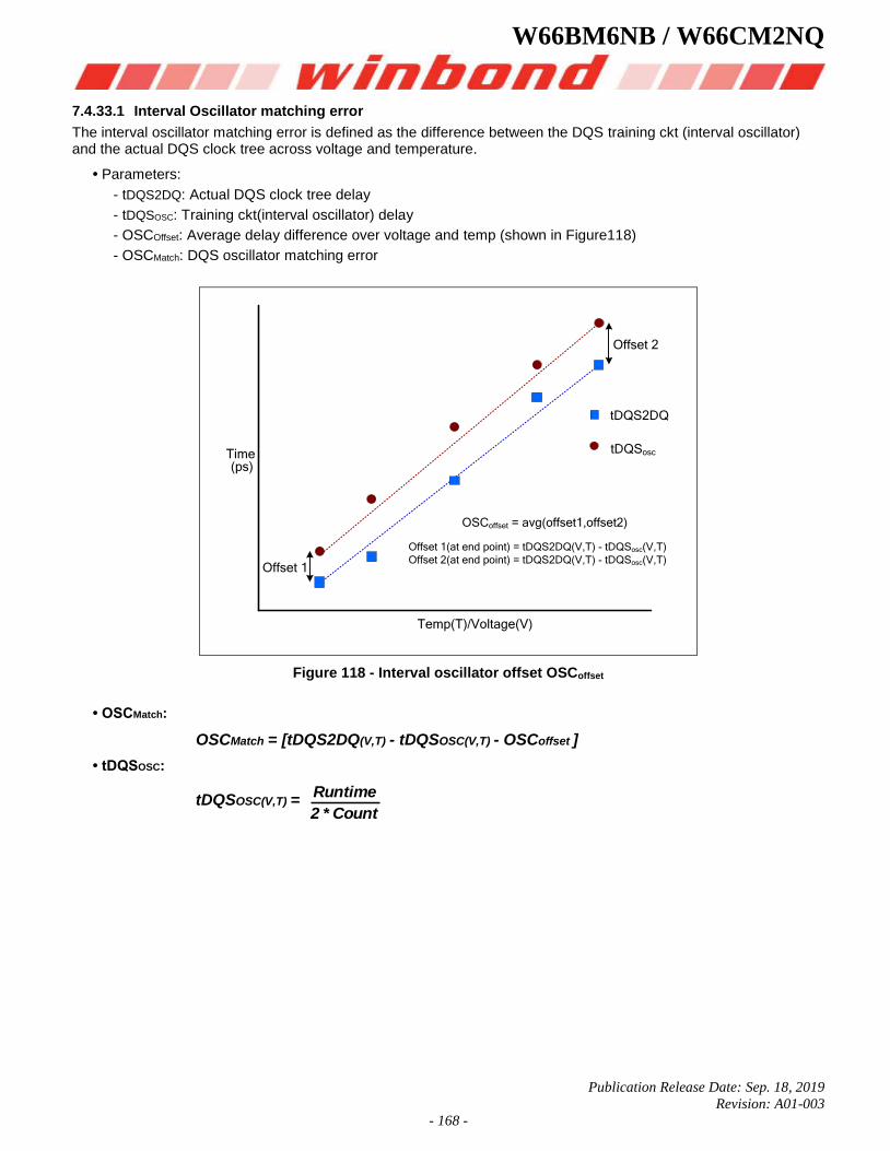
W66BM6NB / W66CM2NQ
Publication Release Date: Sep. 18, 2019
Revision: A01-003
- 168 -
7.4.33.1 Interval Oscillator matching error
The interval oscillator matching error is defined as the difference between the DQS training ckt (interval oscillator) and the actual DQS clock tree across voltage and temperature.
• Parameters:
- tDQS2DQ: Actual DQS clock tree delay
- tDQSOSC: Training ckt(interval oscillator) delay
- OSCOffset: Average delay difference over voltage and temp (shown in Figure118)
- OSCMatch: DQS oscillator matching error
tDQS2DQ
tDQSosc
Offset 2
Offset 1
Temp(T)/Voltage(V)
OSCoffset = avg(offset1,offset2)
Offset 1(at end point) = tDQS2DQ(V,T) - tDQSosc(V,T)
Offset 2(at end point) = tDQS2DQ(V,T) - tDQSosc(V,T)
Time (ps)
Figure 118 - Interval oscillator offset OSCoffset
• OSCMatch:
OSCMatch = [tDQS2DQ(V,T) - tDQSOSC(V,T) - OSCoffset ]
• tDQSOSC:
tDQSOSC(V,T) = Count * 2
Runtime
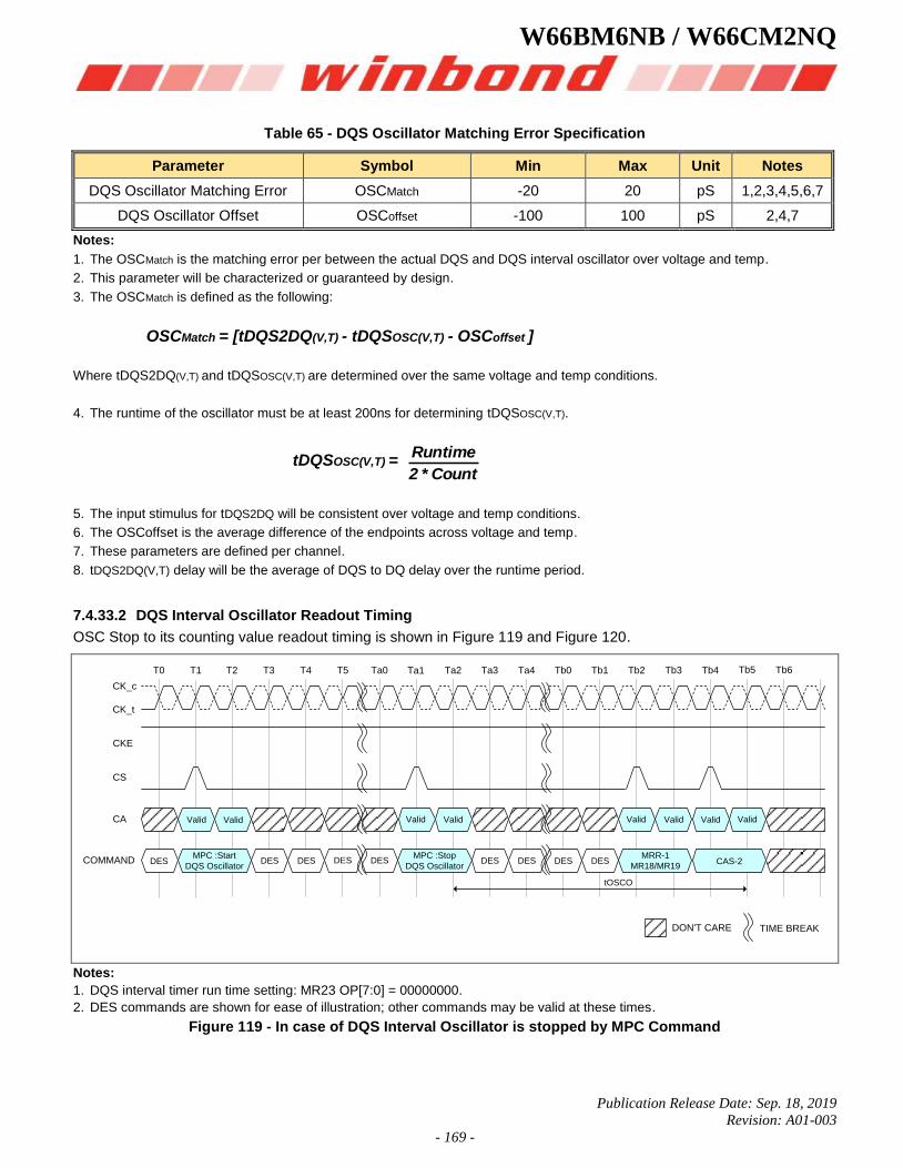
W66BM6NB / W66CM2NQ
Publication Release Date: Sep. 18, 2019
Revision: A01-003
- 169 -
Table 65 - DQS Oscillator Matching Error Specification
Parameter Symbol Min Max Unit Notes
DQS Oscillator Matching Error OSCMatch -20 20 pS 1,2,3,4,5,6,7
DQS Oscillator Offset OSCoffset -100 100 pS 2,4,7
Notes:
1. The OSCMatch is the matching error per between the actual DQS and DQS interval oscillator over voltage and temp.
2. This parameter will be characterized or guaranteed by design.
3. The OSCMatch is defined as the following:
OSCMatch = [tDQS2DQ(V,T) - tDQSOSC(V,T) - OSCoffset ]
Where tDQS2DQ(V,T) and tDQSOSC(V,T) are determined over the same voltage and temp conditions.
4. The runtime of the oscillator must be at least 200ns for determining tDQSOSC(V,T).
tDQSOSC(V,T) = Count * 2
Runtime
5. The input stimulus for tDQS2DQ will be consistent over voltage and temp conditions.
6. The OSCoffset is the average difference of the endpoints across voltage and temp.
7. These parameters are defined per channel.
8. tDQS2DQ(V,T) delay will be the average of DQS to DQ delay over the runtime period.
7.4.33.2 DQS Interval Oscillator Readout Timing
OSC Stop to its counting value readout timing is shown in Figure 119 and Figure 120.
CK_c
CK_t
COMMAND
T0 T1 T2 T3 T4 T5 Ta0 Ta1 Ta2 Ta3 Ta4 Tb0 Tb1 Tb2 Tb3 Tb4 Tb5 Tb6
tOSCO
ValidCA
CS
DES DES DES DESDES
Valid Valid Valid ValidValidValid
CKE
Valid
MPC :Start
DQS OscillatorDES DES
MPC :Stop
DQS OscillatorDES DES
MRR-1
MR18/MR19CAS-2
TIME BREAKDON'T CARE
Notes:
1. DQS interval timer run time setting: MR23 OP[7:0] = 00000000.
2. DES commands are shown for ease of illustration; other commands may be valid at these times.
Figure 119 - In case of DQS Interval Oscillator is stopped by MPC Command
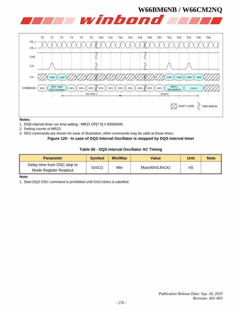
W66BM6NB / W66CM2NQ
Publication Release Date: Sep. 18, 2019
Revision: A01-003
- 170 -
CK_c
CK_t
COMMAND
T0 T1 T2 T3 T4 T5 Ta0 Ta1 Ta2 Ta3 Ta4 Tb0 Tb1 Tb2 Tb3 Tb4 Tb5 Tb6
tOSCO
ValidCA
CS
DES DES DES DESDES
Valid ValidValidValid
CKE
Valid
MPC :Start
DQS OscillatorDES DES DES DES
MRR-1
MR18/MR19CAS-2DES DES
See Note 2
TIME BREAKDON'T CARE
Notes:
1. DQS interval timer run time setting : MR23 OP[7:0] ≠ 00000000.
2. Setting counts of MR23.
3. DES commands are shown for ease of illustration; other commands may be valid at these times.
Figure 120 - In case of DQS Interval Oscillator is stopped by DQS interval timer
Table 66 - DQS Interval Oscillator AC Timing
Parameter Symbol Min/Max Value Unit Note
Delay time from OSC stop to
Mode Register Readout tOSCO Min Max(40nS,8nCK) nS
Note:
1. Start DQS OSC command is prohibited until tOSCO(Min) is satisfied.
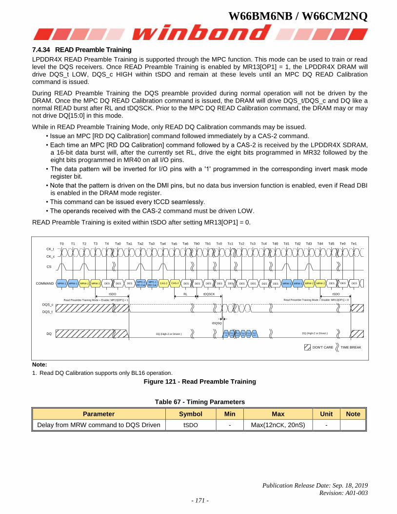
W66BM6NB / W66CM2NQ
Publication Release Date: Sep. 18, 2019
Revision: A01-003
- 171 -
7.4.34 READ Preamble Training
LPDDR4X READ Preamble Training is supported through the MPC function. This mode can be used to train or read level the DQS receivers. Once READ Preamble Training is enabled by MR13[OP1] = 1, the LPDDR4X DRAM will drive DQS_t LOW, DQS_c HIGH within tSDO and remain at these levels until an MPC DQ READ Calibration command is issued.
During READ Preamble Training the DQS preamble provided during normal operation will not be driven by the DRAM. Once the MPC DQ READ Calibration command is issued, the DRAM will drive DQS_t/DQS_c and DQ like a normal READ burst after RL and tDQSCK. Prior to the MPC DQ READ Calibration command, the DRAM may or may not drive DQ[15:0] in this mode.
While in READ Preamble Training Mode, only READ DQ Calibration commands may be issued.
• Issue an MPC [RD DQ Calibration] command followed immediately by a CAS-2 command.
• Each time an MPC [RD DQ Calibration] command followed by a CAS-2 is received by the LPDDR4X SDRAM, a 16-bit data burst will, after the currently set RL, drive the eight bits programmed in MR32 followed by the eight bits programmed in MR40 on all I/O pins.
• The data pattern will be inverted for I/O pins with a '1' programmed in the corresponding invert mask mode register bit.
• Note that the pattern is driven on the DMI pins, but no data bus inversion function is enabled, even if Read DBI is enabled in the DRAM mode register.
• This command can be issued every tCCD seamlessly.
• The operands received with the CAS-2 command must be driven LOW.
READ Preamble Training is exited within tSDO after setting MR13[OP1] = 0.
T0 T1 T2 T3 T4 Ta2 Ta3 Ta5Ta0 Ta1 Ta4 Tc4 Td0Tc2 Td1 Td4 Td5Td2 Td3 Te0
tDQSCK
tDQSQ
CK_t
CK_c
CS
COMMAND
DQS_c
DQS_t
DQ
MRW-1 DES DES DESMPC-1
RD Cal.CAS-2 CAS-2 DES DES MRW-2 MRW-2 DES DES
Tc3
tSDO
Tb0 Tb1 Tc0 Tc1
DES DES DES DES DES
Te1
tSDORL
Ta6
TIME BREAKDON'T CARE
MRW-1 MRW-2 MRW-2MPC-1
RD Cal.MRW-1 MRW-1DES DES DES
Read Preamble Training Mode = Enable: MR13[OP1] = 1 Read Preamble Training Mode = Disable: MR13[OP1] = 0
DQ (High-Z or Driven ) DQ (High-Z or Driven )Dout
n0
Dout
n1
Dout
n12
Dout n13
Dout
n14
Dout
n15
Note:
1. Read DQ Calibration supports only BL16 operation.
Figure 121 - Read Preamble Training
Table 67 - Timing Parameters
Parameter Symbol Min Max Unit Note
Delay from MRW command to DQS Driven tSDO - Max(12nCK, 20nS) -
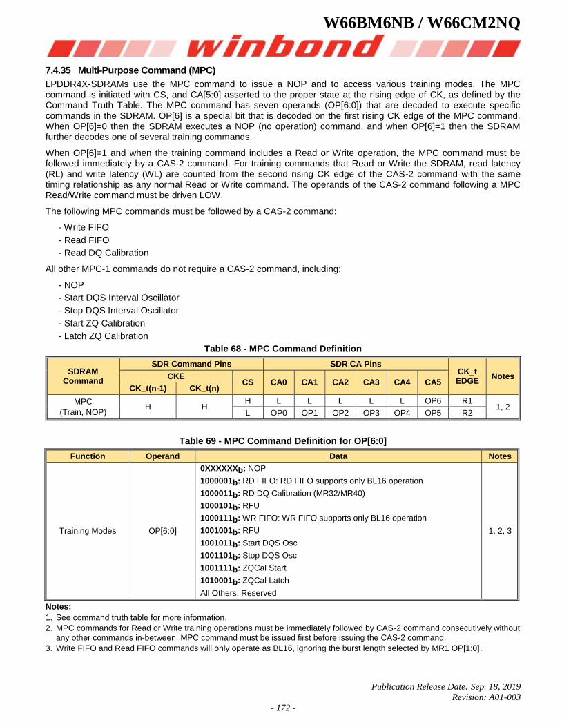
W66BM6NB / W66CM2NQ
Publication Release Date: Sep. 18, 2019
Revision: A01-003
- 172 -
7.4.35 Multi-Purpose Command (MPC)
LPDDR4X-SDRAMs use the MPC command to issue a NOP and to access various training modes. The MPC command is initiated with CS, and CA[5:0] asserted to the proper state at the rising edge of CK, as defined by the Command Truth Table. The MPC command has seven operands (OP[6:0]) that are decoded to execute specific commands in the SDRAM. OP[6] is a special bit that is decoded on the first rising CK edge of the MPC command. When OP[6]=0 then the SDRAM executes a NOP (no operation) command, and when OP[6]=1 then the SDRAM further decodes one of several training commands.
When OP[6]=1 and when the training command includes a Read or Write operation, the MPC command must be followed immediately by a CAS-2 command. For training commands that Read or Write the SDRAM, read latency (RL) and write latency (WL) are counted from the second rising CK edge of the CAS-2 command with the same timing relationship as any normal Read or Write command. The operands of the CAS-2 command following a MPC Read/Write command must be driven LOW.
The following MPC commands must be followed by a CAS-2 command:
- Write FIFO
- Read FIFO
- Read DQ Calibration
All other MPC-1 commands do not require a CAS-2 command, including:
- NOP
- Start DQS Interval Oscillator
- Stop DQS Interval Oscillator
- Start ZQ Calibration
- Latch ZQ Calibration
Table 68 - MPC Command Definition
SDRAM Command
SDR Command Pins SDR CA Pins CK_t EDGE
Notes CKE CS CA0 CA1 CA2 CA3 CA4 CA5
CK_t(n-1) CK_t(n)
MPC
(Train, NOP) H H
H L L L L L OP6 R1 1, 2
L OP0 OP1 OP2 OP3 OP4 OP5 R2
Table 69 - MPC Command Definition for OP[6:0]
Function Operand Data Notes
Training Modes OP[6:0]
0XXXXXXb: NOP
1000001b: RD FIFO: RD FIFO supports only BL16 operation
1000011b: RD DQ Calibration (MR32/MR40)
1000101b: RFU
1000111b: WR FIFO: WR FIFO supports only BL16 operation
1001001b: RFU
1001011b: Start DQS Osc
1001101b: Stop DQS Osc
1001111b: ZQCal Start
1010001b: ZQCal Latch
All Others: Reserved
1, 2, 3
Notes:
1. See command truth table for more information.
2. MPC commands for Read or Write training operations must be immediately followed by CAS-2 command consecutively without any other commands in-between. MPC command must be issued first before issuing the CAS-2 command.
3. Write FIFO and Read FIFO commands will only operate as BL16, ignoring the burst length selected by MR1 OP[1:0].
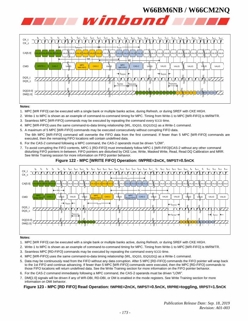
W66BM6NB / W66CM2NQ
Publication Release Date: Sep. 18, 2019
Revision: A01-003
- 173 -
VALID VALID VALID VALID VALID VALID VALID VALID VALID VALID VALID VALID VALID VALID VALID VALID VALID VALID VALID VALID VALID VALID VALID VALID VALID VALID VALID VALID
WRITE-1 CAS-2 VALIDMPC
WR FIFOCAS-2 VALID
MPC
WR FIFOCAS-2 VALID VALID VALID VALID VALIDVALID
D0 D1 D2 D3 D8 D9 D10 D11 D12 D13 D14 D15 D0 D1 D12 D13 D14 D15 D0 D1 D12 D13 D14 D15
t0 t1 t2 t3 t4 ta ta+1 ta+2 ta+3 ta+4 ta+5 tb tb+1 tb+2 tb+3 tb+4 tb+5 tc tc+1 tc+2 tc+3 tc+4 td td+1 td+2 te te+1 te+2
CK_c
CK_t
CA[5:0]
CMD
DQS_c
DQS_t
DMI[1:0]
DQ[15:0]D12
tWRWTR tCCD
WL
tDQSS
tWPRE tDQS2DQ tDQS2DQ
WL
tDQSS
Notes:
1. MPC [WR FIFO] can be executed with a single bank or multiple banks active, during Refresh, or during SREF with CKE HIGH.
2. Write-1 to MPC is shown as an example of command-to-command timing for MPC. Timing from Write-1 to MPC [WR-FIFO] is tWRWTR.
3. Seamless MPC [WR-FIFO] commands may be executed by repeating the command every tCCD time.
4. MPC [WR-FIFO] uses the same command-to-data timing relationship (WL, tDQSS, tDQS2DQ) as a Write-1 command.
5. A maximum of 5 MPC [WR-FIFO] commands may be executed consecutively without corrupting FIFO data.
The 6th MPC [WR-FIFO] command will overwrite the FIFO data from the first command. If fewer than 5 MPC [WR-FIFO] commands are executed, then the remaining FIFO locations will contain undefined data.
6. For the CAS-2 command following a MPC command, the CAS-2 operands must be driven “LOW”.
7. To avoid corrupting the FIFO contents, MPC-1 [RD-FIFO] must immediately follow MPC-1 [WR-FIFO]/CAS-2 without any other command disturbing FIFO pointers in-between. FIFO pointers are disturbed by CKE Low, Write, Masked Write, Read, Read DQ Calibration and MRR. See Write Training session for more information on FIFO pointer behavior.
Figure 122 - MPC [WRITE FIFO] Operation: tWPRE=2nCK, tWPST=0.5nCK
t0
CK_c
CK_t
VALID VALID VALID VALID VALID VALID VALID VALID VALID VALID VALID VALID VALID VALID VALID VALID VALID VALID VALID VALID VALID VALID VALID VALID VALID VALID VALID VALID VALID VALID VALID VALID VALID VALID
MPC
Write FIFOCAS-2 VALID VALID VALID
MPC
Read FIFOCAS-2 VALID
MPC
Read FIFOCAS-2 VALID VALID VALID VALID VALID VALID VALID
t1 t2 t3 t4 ta ta+1 ta+2 ta+3 tf+3 tf+4tb tb+1 tb+2 tb+3 tb+4 tb+5 tf tf+1tc+2 tc+3 tc+4 td td+1 td+2 te te+1 tf+2tc+5 tc+6 tc+7 td+3 td+4 td+5
CA[5:0]
CMD
DQS_c
DQS_t
DMI[1:0]
DQ[15:0]
tCCD
RL
tWTR
WL
tDQSS
tDQS2DQ tRPRE
tDQSCK
tRPST
D0 D1 D13 D14 D15D12 D0 D1 D13 D14 D15D12 D0 D1 D13 D14 D15D12
Notes:
1. MPC [WR FIFO] can be executed with a single bank or multiple banks active, during Refresh, or during SREF with CKE HIGH.
2. Write-1 to MPC is shown as an example of command-to-command timing for MPC. Timing from Write-1 to MPC [WR-FIFO] is tWRWTR.
3. Seamless MPC [RD-FIFO] commands may be executed by repeating the command every tCCD time.
4. MPC [WR-FIFO] uses the same command-to-data timing relationship (WL, tDQSS, tDQS2DQ) as a Write-1 command.
5. Data may be continuously read from the FIFO without any data corruption. After 5 MPC [RD-FIFO] commands the FIFO pointer will wrap back to the 1st FIFO and continue advancing. If fewer than 5 MPC [WR-FIFO] commands were executed, then the MPC [RD-FIFO] commands to those FIFO locations will return undefined data. See the Write Training section for more information on the FIFO pointer behavior.
6. For the CAS-2 command immediately following a MPC command, the CAS-2 operands must be driven “LOW”.
7. DMI[1:0] signals will be driven if any of WR-DBI, RD-DBI, or DM is enabled in the mode registers. See Write Training section for more information on DMI behavior.
Figure 123 - MPC [RD FIFO] Read Operation: tWPRE=2nCK, tWPST=0.5nCK, tRPRE=toggling, tRPST=1.5nCK
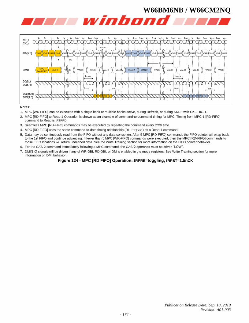
W66BM6NB / W66CM2NQ
Publication Release Date: Sep. 18, 2019
Revision: A01-003
- 174 -
VALID VALID VALID VALID VALID VALID VALID VALID VALID VALID VALID VALID VALID VALID VALID VALID VALID VALID VALID VALID VALID VALID VALID VALID VALID VALID VALID VALID VALID VALID
MPC
Read FIFOCAS-2 VALID VALIDVALID VALID Read-1VALID CAS-2 VALIDVALID VALID VALID VALIDVALID
D0 D1 D13 D14 D15D2 D0 D1 D13 D14 D15D10 D11 D12
t0 t1 t2 t3 t4 ta ta+1 ta+2 ta+3 tbta+4 tb+1 tc+3 te te+4tc+4tc+1 td td+3tc te+5tc+2 td+2td+1 te+1 te+2 te+3
CK_c
CK_t
CA[5:0]
CMD
DQS_c
DQS_t
DMI[1:0]
DQ[15:0]
tRTRRD
RL
RL
tDQSCK tDQSCK
tRPRE tRPREtRPST tRPST
tc+5
Notes:
1. MPC [WR FIFO] can be executed with a single bank or multiple banks active, during Refresh, or during SREF with CKE HIGH.
2. MPC [RD-FIFO] to Read-1 Operation is shown as an example of command-to-command timing for MPC. Timing from MPC-1 [RD-FIFO] command to Read is tRTRRD.
3. Seamless MPC [RD-FIFO] commands may be executed by repeating the command every tCCD time.
4. MPC [RD-FIFO] uses the same command-to-data timing relationship (RL, tDQSCK) as a Read-1 command.
5. Data may be continuously read from the FIFO without any data corruption. After 5 MPC [RD-FIFO] commands the FIFO pointer will wrap back to the 1st FIFO and continue advancing. If fewer than 5 MPC [WR-FIFO] commands were executed, then the MPC [RD-FIFO] commands to those FIFO locations will return undefined data. See the Write Training section for more information on the FIFO pointer behavior.
6. For the CAS-2 command immediately following a MPC command, the CAS-2 operands must be driven “LOW”.
7. DMI[1:0] signals will be driven if any of WR-DBI, RD-DBI, or DM is enabled in the mode registers. See Write Training section for more information on DMI behavior.
Figure 124 - MPC [RD FIFO] Operation: tRPRE=toggling, tRPST=1.5nCK
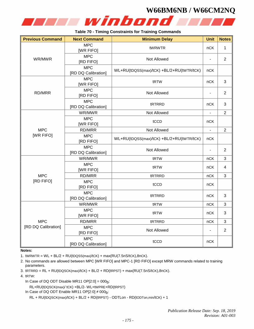
W66BM6NB / W66CM2NQ
Publication Release Date: Sep. 18, 2019
Revision: A01-003
- 175 -
Table 70 - Timing Constraints for Training Commands
Previous Command Next Command Minimum Delay Unit Notes
WR/MWR
MPC
[WR FIFO] tWRWTR nCK 1
MPC
[RD FIFO] Not Allowed - 2
MPC
[RD DQ Calibration] WL+RU(tDQSS(max)/tCK) +BL/2+RU(tWTR/tCK) nCK
RD/MRR
MPC
[WR FIFO] tRTW nCK 3
MPC
[RD FIFO] Not Allowed - 2
MPC
[RD DQ Calibration] tRTRRD nCK 3
MPC
[WR FIFO]
WR/MWR Not Allowed - 2
MPC
[WR FIFO] tCCD nCK
RD/MRR Not Allowed - 2
MPC
[RD FIFO] WL+RU(tDQSS(max)/tCK) +BL/2+RU(tWTR/tCK) nCK
MPC
[RD DQ Calibration] Not Allowed - 2
MPC
[RD FIFO]
WR/MWR tRTW nCK 3
MPC
[WR FIFO] tRTW nCK 4
RD/MRR tRTRRD nCK 3
MPC
[RD FIFO] tCCD nCK
MPC
[RD DQ Calibration] tRTRRD nCK 3
MPC
[RD DQ Calibration]
WR/MWR tRTW nCK 3
MPC
[WR FIFO] tRTW nCK 3
RD/MRR tRTRRD nCK 3
MPC
[RD FIFO] Not Allowed - 2
MPC
[RD DQ Calibration] tCCD nCK
Notes:
1. tWRWTR = WL + BL/2 + RU(tDQSS(max)/tCK) + max(RU(7.5nS/tCK),8nCK).
2. No commands are allowed between MPC [WR FIFO] and MPC-1 [RD FIFO] except MRW commands related to training parameters.
3. tRTRRD = RL + RU(tDQSCK(max)/tCK) + BL/2 + RD(tRPST) + max(RU(7.5nS/tCK),8nCK).
4. tRTW:
In Case of DQ ODT Disable MR11 OP[2:0] = 000b:
RL+RU(tDQSCK(max)/ tCK) +BL/2- WL+tWPRE+RD(tRPST)
In Case of DQ ODT Enable MR11 OP[2:0] ≠ 000b:
RL + RU(tDQSCK(max)/tCK) + BL/2 + RD(tRPST) - ODTLon - RD(tODTon,min/tCK) + 1
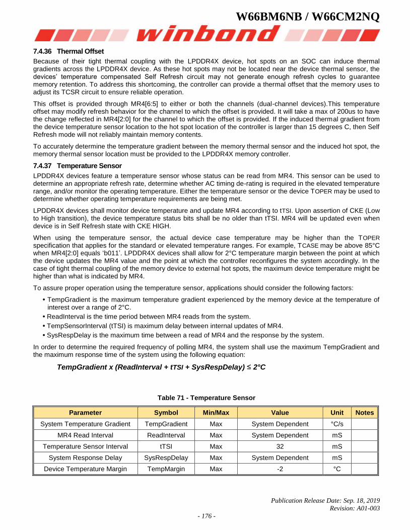
W66BM6NB / W66CM2NQ
Publication Release Date: Sep. 18, 2019
Revision: A01-003
- 176 -
7.4.36 Thermal Offset
Because of their tight thermal coupling with the LPDDR4X device, hot spots on an SOC can induce thermal gradients across the LPDDR4X device. As these hot spots may not be located near the device thermal sensor, the devices’ temperature compensated Self Refresh circuit may not generate enough refresh cycles to guarantee memory retention. To address this shortcoming, the controller can provide a thermal offset that the memory uses to adjust its TCSR circuit to ensure reliable operation.
This offset is provided through MR4[6:5] to either or both the channels (dual-channel devices).This temperature offset may modify refresh behavior for the channel to which the offset is provided. It will take a max of 200us to have the change reflected in MR4[2:0] for the channel to which the offset is provided. If the induced thermal gradient from the device temperature sensor location to the hot spot location of the controller is larger than 15 degrees C, then Self Refresh mode will not reliably maintain memory contents.
To accurately determine the temperature gradient between the memory thermal sensor and the induced hot spot, the memory thermal sensor location must be provided to the LPDDR4X memory controller.
7.4.37 Temperature Sensor
LPDDR4X devices feature a temperature sensor whose status can be read from MR4. This sensor can be used to determine an appropriate refresh rate, determine whether AC timing de-rating is required in the elevated temperature range, and/or monitor the operating temperature. Either the temperature sensor or the device TOPER may be used to determine whether operating temperature requirements are being met.
LPDDR4X devices shall monitor device temperature and update MR4 according to tTSI. Upon assertion of CKE (Low to High transition), the device temperature status bits shall be no older than tTSI. MR4 will be updated even when device is in Self Refresh state with CKE HIGH.
When using the temperature sensor, the actual device case temperature may be higher than the TOPER specification that applies for the standard or elevated temperature ranges. For example, TCASE may be above 85°C when MR4[2:0] equals ‘b011’. LPDDR4X devices shall allow for 2°C temperature margin between the point at which the device updates the MR4 value and the point at which the controller reconfigures the system accordingly. In the case of tight thermal coupling of the memory device to external hot spots, the maximum device temperature might be higher than what is indicated by MR4.
To assure proper operation using the temperature sensor, applications should consider the following factors:
• TempGradient is the maximum temperature gradient experienced by the memory device at the temperature of interest over a range of 2°C.
• ReadInterval is the time period between MR4 reads from the system.
• TempSensorInterval (tTSI) is maximum delay between internal updates of MR4.
• SysRespDelay is the maximum time between a read of MR4 and the response by the system.
In order to determine the required frequency of polling MR4, the system shall use the maximum TempGradient and the maximum response time of the system using the following equation:
TempGradient x (ReadInterval + tTSI + SysRespDelay) ≤ 2°C
Table 71 - Temperature Sensor
Parameter Symbol Min/Max Value Unit Notes
System Temperature Gradient TempGradient Max System Dependent °C/s
MR4 Read Interval ReadInterval Max System Dependent mS
Temperature Sensor Interval tTSI Max 32 mS
System Response Delay SysRespDelay Max System Dependent mS
Device Temperature Margin TempMargin Max -2 °C
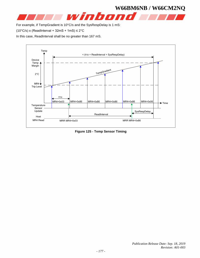
W66BM6NB / W66CM2NQ
Publication Release Date: Sep. 18, 2019
Revision: A01-003
- 177 -
For example, if TempGradient is 10°C/s and the SysRespDelay is 1 mS:
(10°C/s) x (ReadInterval + 32mS + 1mS) ≤ 2°C
In this case, ReadInterval shall be no greater than 167 mS.
Temp
Device
Temp
Margin
MR4
Trip Level
Temperature
Sensor
Update
Host
MR4 Read MRR MR4=0x03
MR4=0x86
Readlnterval
MRR MR4=0x86
tTSI
Time
SysRespDelay
2°C
< (tTSI + Readlnterval + SysRespDelay)
TempGradient
MR4=0x03 MR4=0x86 MR4=0x86 MR4=0x86 MR4=0x06
Figure 125 - Temp Sensor Timing
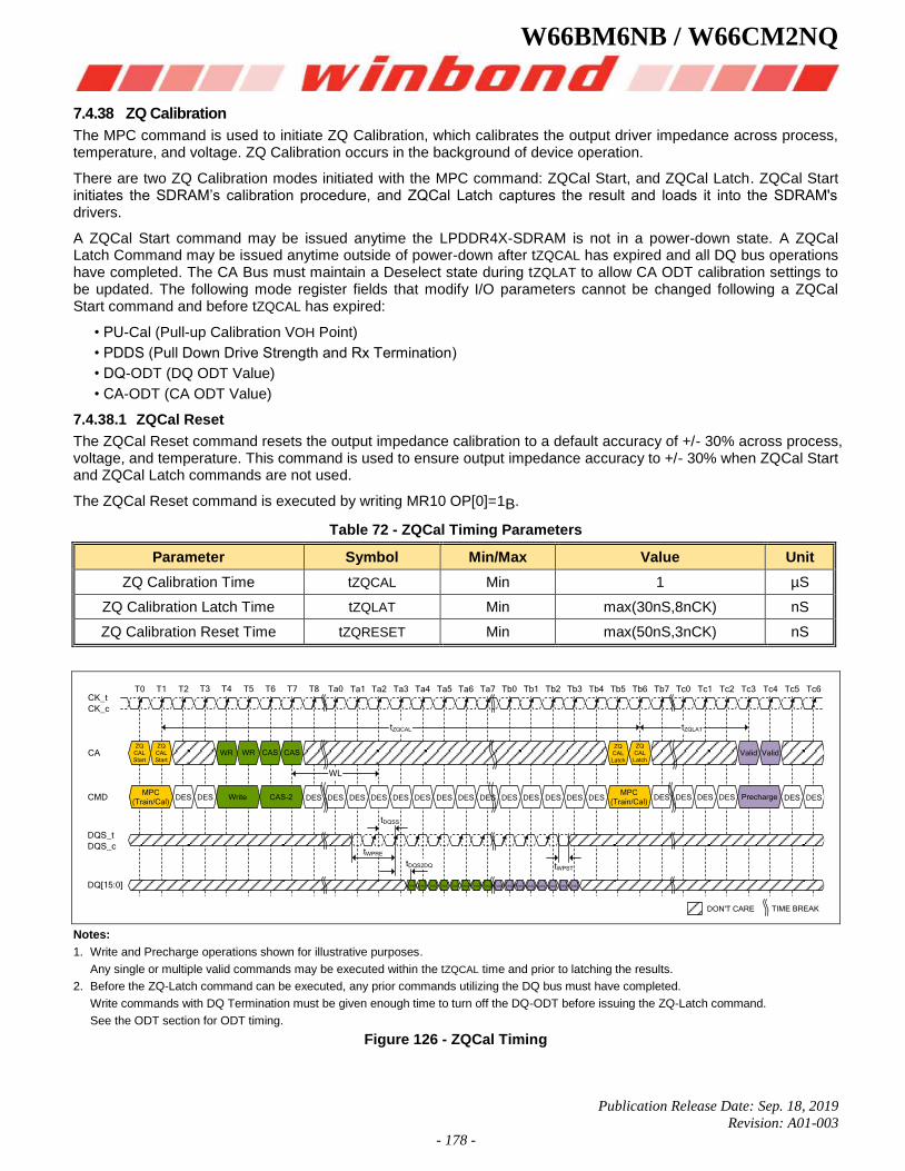
W66BM6NB / W66CM2NQ
Publication Release Date: Sep. 18, 2019
Revision: A01-003
- 178 -
7.4.38 ZQ Calibration
The MPC command is used to initiate ZQ Calibration, which calibrates the output driver impedance across process, temperature, and voltage. ZQ Calibration occurs in the background of device operation.
There are two ZQ Calibration modes initiated with the MPC command: ZQCal Start, and ZQCal Latch. ZQCal Start initiates the SDRAM’s calibration procedure, and ZQCal Latch captures the result and loads it into the SDRAM's drivers.
A ZQCal Start command may be issued anytime the LPDDR4X-SDRAM is not in a power-down state. A ZQCal Latch Command may be issued anytime outside of power-down after tZQCAL has expired and all DQ bus operations have completed. The CA Bus must maintain a Deselect state during tZQLAT to allow CA ODT calibration settings to be updated. The following mode register fields that modify I/O parameters cannot be changed following a ZQCal Start command and before tZQCAL has expired:
• PU-Cal (Pull-up Calibration VOH Point)
• PDDS (Pull Down Drive Strength and Rx Termination)
• DQ-ODT (DQ ODT Value)
• CA-ODT (CA ODT Value)
7.4.38.1 ZQCal Reset
The ZQCal Reset command resets the output impedance calibration to a default accuracy of +/- 30% across process, voltage, and temperature. This command is used to ensure output impedance accuracy to +/- 30% when ZQCal Start and ZQCal Latch commands are not used.
The ZQCal Reset command is executed by writing MR10 OP[0]=1B.
Table 72 - ZQCal Timing Parameters
Parameter Symbol Min/Max Value Unit
ZQ Calibration Time tZQCAL Min 1 µS
ZQ Calibration Latch Time tZQLAT Min max(30nS,8nCK) nS
ZQ Calibration Reset Time tZQRESET Min max(50nS,3nCK) nS
ZQ
CAL
Start
ZQ
CAL
StartWR WR CAS CAS
ZQ
CAL
Latch
ZQ
CAL
LatchValid Valid
WriteMPC
(Train/Cal)DES DES CAS-2 DES DES DES DES DES DES DES DES DES DES DES DES DES DES
MPC
(Train/Cal)DES DES DES DES DES DESPrecharge
Valid Valid Valid Valid Valid Valid Valid Valid Valid Valid Valid Valid Valid Valid Valid Valid
TIME BREAKDON'T CARE
tZQLATtZQCAL
WL
tDQSS
tDQS2DQ
tWPRE
tWPST
CK_c
CK_t
CA
CMD
DQS_c
DQS_t
DQ[15:0]
T0 T1 T2 T3 T4 T7 T8 Ta1T5 T6 Ta0 Tb1 Tb2Ta7 Tb3 Tb6 Tb7Tb4 Tb5 Tc0Tb0Ta3 Ta4 Ta5 Ta6 Tc1Ta2 Tc4 Tc5Tc2 Tc6Tc3
Notes:
1. Write and Precharge operations shown for illustrative purposes.
Any single or multiple valid commands may be executed within the tZQCAL time and prior to latching the results.
2. Before the ZQ-Latch command can be executed, any prior commands utilizing the DQ bus must have completed.
Write commands with DQ Termination must be given enough time to turn off the DQ-ODT before issuing the ZQ-Latch command.
See the ODT section for ODT timing.
Figure 126 - ZQCal Timing
W66BM6NB / W66CM2NQ
Publication Release Date: Sep. 18, 2019
Revision: A01-003
- 179 -
7.4.38.2 ZQ External Resistor, Tolerance, and Capacitive Loading
To use the ZQ calibration function, a 240 ohm ±1% tolerance external resistor must be connected between the ZQ pin and VDDQ.
If the system configuration shares the CA bus to form an x32 (or wider) channel, the ZQ pin of each die’s x16 channel shall use a separate ZQCal resistor.
If the system configuration has more than one rank, and if the ZQ pins of both ranks are attached to a single resistor, then the SDRAM controller must ensure that the ZQCal’s don’t overlap.
The total capacitive loading on the ZQ pin must be limited to 25pF.
Example: If a system configuration shares a CA bus between ‘n’ channels to form a n*16 wide bus, and no means are available to control the ZQCal separately for each channel (i.e., separate CS, CKE, or CK), then each x16 channel must have a separate ZQCal resistor.
Example: For an x32, two rank system, each x16 channel must have its own ZQCal resistor, but the ZQCal resistor can be shared between ranks on each x16 channel. In this configuration, the CS signal can be used to ensure that the ZQCal commands for Rank[0] and Rank[1] don't overlap.
7.4.39 Pull Up/Pull Down Driver Characteristics and Calibration
Table 73 - Pull-down Driver Characteristics, with ZQ Calibration
RONPD,nom Resistor Min Nom Max Unit
40 Ohm RON40PD 0.9 1 1.1 RZQ/6
48 Ohm RON48PD 0.9 1 1.1 RZQ/5
60 Ohm RON60PD 0.9 1 1.1 RZQ/4
80 Ohm RON80PD 0.9 1 1.1 RZQ/3
120 Ohm RON120PD 0.9 1 1.1 RZQ/2
240 Ohm RON240PD 0.9 1 1.1 RZQ/1
Note:
1. All value are after ZQ Calibration. Without ZQ Calibration RONPD values are ± 30%.
Table 74 - Terminated Pull-Up Characteristics, with ZQ Calibration
VOHPU,nom VOH,nom(mV) Min Nom Max Unit
VDDQ*0.5 300 0.9 1 1.1 VOH,nom
VDDQ*0.6 360 0.9 1 1.1 VOH,nom
Notes:
1. All values are after ZQ Calibration. Without ZQ Calibration VOH(nom) values are ± 30%.
2. VOH,nom (mV) values are based on a nominal VDDQ = 0.6V.
Table 75 - Terminated Valid Calibration Points
VOHPU,nom SOC ODT Value
240 120 80 60 48 40
VDDQ*0.5 VALID VALID VALID VALID VALID VALID
VDDQ*0.6 DNU VALID DNU VALID DNU DNU
Notes:
1. Once the output is calibrated for a given VOH(nom) calibration point, the ODT value may be changed without recalibration.
2. If the VOH(nom) calibration point is changed, then re-calibration is required.
3. DNU = Do Not Use.
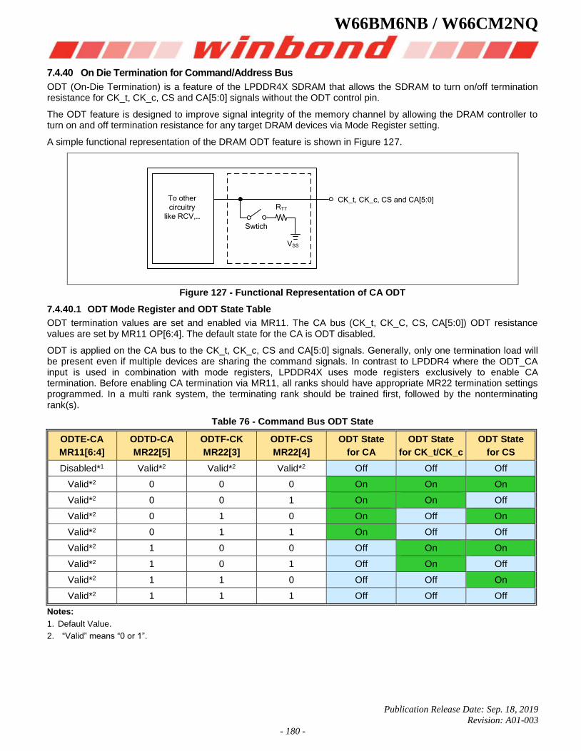
W66BM6NB / W66CM2NQ
Publication Release Date: Sep. 18, 2019
Revision: A01-003
- 180 -
7.4.40 On Die Termination for Command/Address Bus
ODT (On-Die Termination) is a feature of the LPDDR4X SDRAM that allows the SDRAM to turn on/off termination resistance for CK_t, CK_c, CS and CA[5:0] signals without the ODT control pin.
The ODT feature is designed to improve signal integrity of the memory channel by allowing the DRAM controller to turn on and off termination resistance for any target DRAM devices via Mode Register setting.
A simple functional representation of the DRAM ODT feature is shown in Figure 127.
To other
circuitry
like RCV,…
RTT
Swtich
VSS
CK_t, CK_c, CS and CA[5:0]
Figure 127 - Functional Representation of CA ODT
7.4.40.1 ODT Mode Register and ODT State Table
ODT termination values are set and enabled via MR11. The CA bus (CK_t, CK_C, CS, CA[5:0]) ODT resistance values are set by MR11 OP[6:4]. The default state for the CA is ODT disabled.
ODT is applied on the CA bus to the CK_t, CK_c, CS and CA[5:0] signals. Generally, only one termination load will be present even if multiple devices are sharing the command signals. In contrast to LPDDR4 where the ODT_CA input is used in combination with mode registers, LPDDR4X uses mode registers exclusively to enable CA termination. Before enabling CA termination via MR11, all ranks should have appropriate MR22 termination settings programmed. In a multi rank system, the terminating rank should be trained first, followed by the nonterminating rank(s).
Table 76 - Command Bus ODT State
ODTE-CA
MR11[6:4]
ODTD-CA
MR22[5]
ODTF-CK
MR22[3]
ODTF-CS
MR22[4]
ODT State
for CA
ODT State
for CK_t/CK_c
ODT State
for CS
Disabled*1 Valid*2 Valid*2 Valid*2 Off Off Off
Valid*2 0 0 0 On On On
Valid*2 0 0 1 On On Off
Valid*2 0 1 0 On Off On
Valid*2 0 1 1 On Off Off
Valid*2 1 0 0 Off On On
Valid*2 1 0 1 Off On Off
Valid*2 1 1 0 Off Off On
Valid*2 1 1 1 Off Off Off
Notes:
1. Default Value.
2. “Valid” means “0 or 1”.
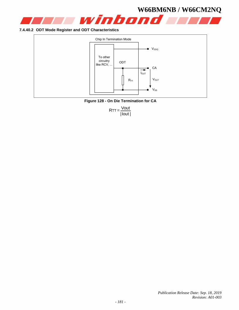
W66BM6NB / W66CM2NQ
Publication Release Date: Sep. 18, 2019
Revision: A01-003
- 181 -
7.4.40.2 ODT Mode Register and ODT Characteristics
IOUT
VOUT
CA
VSS
ODT
To other
circuitry
like RCV, ...
RTT
VDDQ
Chip In Termination Mode
Figure 128 - On Die Termination for CA
RTT =| Iout |
Vout
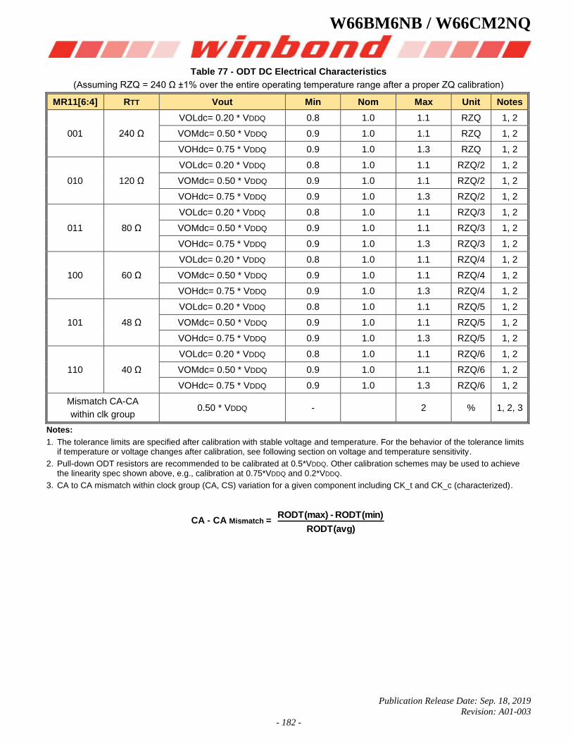
W66BM6NB / W66CM2NQ
Publication Release Date: Sep. 18, 2019
Revision: A01-003
- 182 -
Table 77 - ODT DC Electrical Characteristics
(Assuming RZQ = 240 Ω ±1% over the entire operating temperature range after a proper ZQ calibration)
MR11[6:4] RTT Vout Min Nom Max Unit Notes
001 240 Ω
VOLdc= 0.20 * VDDQ 0.8 1.0 1.1 RZQ 1, 2
VOMdc= 0.50 * VDDQ 0.9 1.0 1.1 RZQ 1, 2
VOHdc= 0.75 * VDDQ 0.9 1.0 1.3 RZQ 1, 2
010 120 Ω
VOLdc= 0.20 * VDDQ 0.8 1.0 1.1 RZQ/2 1, 2
VOMdc= 0.50 * VDDQ 0.9 1.0 1.1 RZQ/2 1, 2
VOHdc= 0.75 * VDDQ 0.9 1.0 1.3 RZQ/2 1, 2
011 80 Ω
VOLdc= 0.20 * VDDQ 0.8 1.0 1.1 RZQ/3 1, 2
VOMdc= 0.50 * VDDQ 0.9 1.0 1.1 RZQ/3 1, 2
VOHdc= 0.75 * VDDQ 0.9 1.0 1.3 RZQ/3 1, 2
100 60 Ω
VOLdc= 0.20 * VDDQ 0.8 1.0 1.1 RZQ/4 1, 2
VOMdc= 0.50 * VDDQ 0.9 1.0 1.1 RZQ/4 1, 2
VOHdc= 0.75 * VDDQ 0.9 1.0 1.3 RZQ/4 1, 2
101 48 Ω
VOLdc= 0.20 * VDDQ 0.8 1.0 1.1 RZQ/5 1, 2
VOMdc= 0.50 * VDDQ 0.9 1.0 1.1 RZQ/5 1, 2
VOHdc= 0.75 * VDDQ 0.9 1.0 1.3 RZQ/5 1, 2
110 40 Ω
VOLdc= 0.20 * VDDQ 0.8 1.0 1.1 RZQ/6 1, 2
VOMdc= 0.50 * VDDQ 0.9 1.0 1.1 RZQ/6 1, 2
VOHdc= 0.75 * VDDQ 0.9 1.0 1.3 RZQ/6 1, 2
Mismatch CA-CA
within clk group 0.50 * VDDQ - 2 % 1, 2, 3
Notes:
1. The tolerance limits are specified after calibration with stable voltage and temperature. For the behavior of the tolerance limits if temperature or voltage changes after calibration, see following section on voltage and temperature sensitivity.
2. Pull-down ODT resistors are recommended to be calibrated at 0.5*VDDQ. Other calibration schemes may be used to achieve the linearity spec shown above, e.g., calibration at 0.75*VDDQ and 0.2*VDDQ.
3. CA to CA mismatch within clock group (CA, CS) variation for a given component including CK_t and CK_c (characterized).
CA - CA Mismatch = RODT(avg)
RODT(min) - RODT(max)
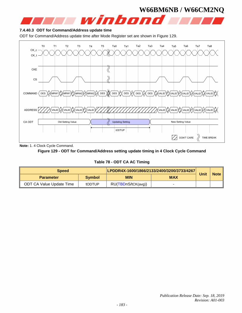
W66BM6NB / W66CM2NQ
Publication Release Date: Sep. 18, 2019
Revision: A01-003
- 183 -
7.4.40.3 ODT for Command/Address update time
ODT for Command/Address update time after Mode Register set are shown in Figure 129.
DES MRW1 MRW1 MRW2 MRW2 DES DES DES DES DES VALID1
VALIDVALID1
VALID1
VALID1
VALID VALID VALID VALID VALIDVALID VALID VALID VALID
TIME BREAKDON'T CARE
tODTUP
New Setting ValueUpdating SettingOld Setting Value
T0 T1 T2 T3 T4 T5 Ta0 Ta1 Ta2 Ta3 Ta4 Ta5 Ta6 Ta7 Ta8
COMMAND
CA ODT
CK_c
CK_t
CS
ADDRESS
CKE
Note: 1. 4 Clock Cycle Command.
Figure 129 - ODT for Command/Address setting update timing in 4 Clock Cycle Command
Table 78 - ODT CA AC Timing
Speed LPDDR4X-1600/1866/2133/2400/3200/3733/4267 Unit Note
Parameter Symbol MIN MAX
ODT CA Value Update Time tODTUP RU(TBDnS/tCK(avg)) -
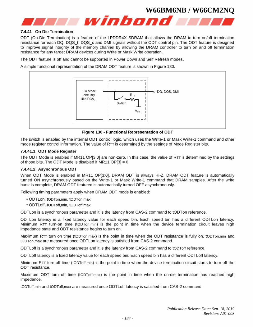
W66BM6NB / W66CM2NQ
Publication Release Date: Sep. 18, 2019
Revision: A01-003
- 184 -
7.4.41 On-Die Termination
ODT (On-Die Termination) is a feature of the LPDDR4X SDRAM that allows the DRAM to turn on/off termination resistance for each DQ, DQS_t, DQS_c and DMI signals without the ODT control pin. The ODT feature is designed to improve signal integrity of the memory channel by allowing the DRAM controller to turn on and off termination resistance for any target DRAM devices during Write or Mask Write operation.
The ODT feature is off and cannot be supported in Power Down and Self Refresh modes.
A simple functional representation of the DRAM ODT feature is shown in Figure 130.
To other
circuitry
like RCV,…
RTT
Swtich
VSS
DQ, DQS, DMI
Figure 130 - Functional Representation of ODT
The switch is enabled by the internal ODT control logic, which uses the Write-1 or Mask Write-1 command and other mode register control information. The value of RTT is determined by the settings of Mode Register bits.
7.4.41.1 ODT Mode Register
The ODT Mode is enabled if MR11 OP[3:0] are non-zero. In this case, the value of RTT is determined by the settings of those bits. The ODT Mode is disabled if MR11 OP[3] = 0.
7.4.41.2 Asynchronous ODT
When ODT Mode is enabled in MR11 OP[3:0], DRAM ODT is always Hi-Z. DRAM ODT feature is automatically turned ON asynchronously based on the Write-1 or Mask Write-1 command that DRAM samples. After the write burst is complete, DRAM ODT featured is automatically turned OFF asynchronously.
Following timing parameters apply when DRAM ODT mode is enabled:
• ODTLon, tODTon,min, tODTon,max
• ODTLoff, tODToff,min, tODToff,max
ODTLon is a synchronous parameter and it is the latency from CAS-2 command to tODTon reference.
ODTLon latency is a fixed latency value for each speed bin. Each speed bin has a different ODTLon latency. Minimum RTT turn-on time (tODTon,min) is the point in time when the device termination circuit leaves high impedance state and ODT resistance begins to turn on.
Maximum RTT turn on time (tODTon,max) is the point in time when the ODT resistance is fully on. tODTon,min and tODTon,max are measured once ODTLon latency is satisfied from CAS-2 command.
ODTLoff is a synchronous parameter and it is the latency from CAS-2 command to tODToff reference.
ODTLoff latency is a fixed latency value for each speed bin. Each speed bin has a different ODTLoff latency.
Minimum RTT turn-off time (tODToff,min) is the point in time when the device termination circuit starts to turn off the ODT resistance.
Maximum ODT turn off time (tODToff,max) is the point in time when the on-die termination has reached high impedance.
tODToff,min and tODToff,max are measured once ODTLoff latency is satisfied from CAS-2 command.
W66BM6NB / W66CM2NQ
Publication Release Date: Sep. 18, 2019
Revision: A01-003
- 185 -
Table 79 - ODTLon and ODTLoff Latency Values
ODTLon Latency*1 ODTLoff Latency*2
Lower Clock
Frequency Limit
(>)
Upper Clock
Frequency Limit
(≤)
tWPRE = 2 tCK
WL Set "A" WL Set "B" WL Set "A" WL Set "B"
N/A N/A N/A N/A 10 266
N/A N/A N/A N/A 266 533
N/A 6 N/A 22 533 800
4 12 20 28 800 1066
4 14 22 32 1066 1333
6 18 24 36 1333 1600
6 20 26 40 1600 1866
8 24 28 44 1866 2133
nCK nCK nCK nCK MHz MHz
Notes:
1. ODTLon is referenced from CAS-2 command. See Figure 131.
2. ODTLoff as shown in table assumes BL=16. For BL32, 8 tCK should be added.
Table 80 - Asynchronous ODT Turn On and Turn Off Timing
Parameter 800 - 2133 MHz Unit
tODTon, min 1.5 nS
tODTon, max 3.5 nS
tODToff, min 1.5 nS
tODToff, max 3.5 nS
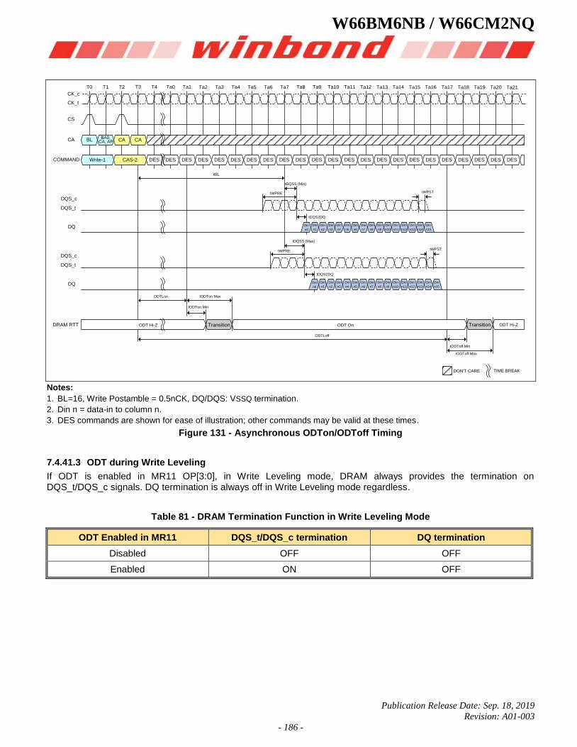
W66BM6NB / W66CM2NQ
Publication Release Date: Sep. 18, 2019
Revision: A01-003
- 186 -
BL CA, AP CACABA0,
Write-1 DESCAS-2 DES DES DES DES DES DES DES DES DES DES DES DES DES DES DES DES DES DES DES DES DES DES
Din
n0
Din
n1
Din
n2
Din
n3
Din
n4
Din
n5
Din
n12
Din
n13
Din
n14
Din
n15
Din
n6
Din
n7
Din
n8
Din
n9
Din
n10
Din
n11
tWPRE
tDQSS (Min)
tDQS2DQ
tWPST
Din
n0
Din
n1
Din
n2
Din
n3
Din
n4
Din
n5
Din
n12
Din
n13
Din
n14
Din
n15
Din
n6
Din
n7
Din
n8
Din
n9
Din
n10
Din
n11
tWPRE
tDQSS (Max)
tDQS2DQ
tWPST
Transition Transition
WL
ODTLon tODTon.Max
tODTon.Min
ODTLoff
tODToff.Max
tODToff.Min
DON'T CARE TIME BREAK
CK_c
CK_t
CS
CA
COMMAND
DQS_c
DQS_t
DQ
DQS_c
DQS_t
DQ
DRAM RTT
T0 T1 T2 T3 T4 Ta0 Ta1 Ta2 Ta3 Ta4 Ta5 Ta6 Ta7 Ta8 Ta9 Ta10 Ta11 Ta12 Ta13 Ta14 Ta15 Ta16 Ta17 Ta18 Ta19 Ta20 Ta21
ODT OnODT Hi-Z ODT Hi-Z
Notes:
1. BL=16, Write Postamble = 0.5nCK, DQ/DQS: VSSQ termination.
2. Din n = data-in to column n.
3. DES commands are shown for ease of illustration; other commands may be valid at these times.
Figure 131 - Asynchronous ODTon/ODToff Timing
7.4.41.3 ODT during Write Leveling
If ODT is enabled in MR11 OP[3:0], in Write Leveling mode, DRAM always provides the termination on DQS_t/DQS_c signals. DQ termination is always off in Write Leveling mode regardless.
Table 81 - DRAM Termination Function in Write Leveling Mode
ODT Enabled in MR11 DQS_t/DQS_c termination DQ termination
Disabled OFF OFF
Enabled ON OFF
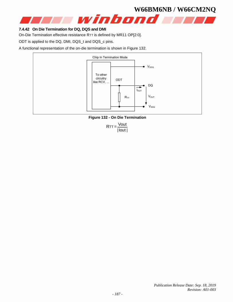
W66BM6NB / W66CM2NQ
Publication Release Date: Sep. 18, 2019
Revision: A01-003
- 187 -
7.4.42 On Die Termination for DQ, DQS and DMI
On-Die Termination effective resistance RTT is defined by MR11 OP[2:0].
ODT is applied to the DQ, DMI, DQS_t and DQS_c pins.
A functional representation of the on-die termination is shown in Figure 132.
IOUT
VOUT
DQ
VSSQ
ODT
To other
circuitry
like RCV, ...
RTT
VDDQ
Chip In Termination Mode
Figure 132 - On Die Termination
RTT =| Iout |
Vout
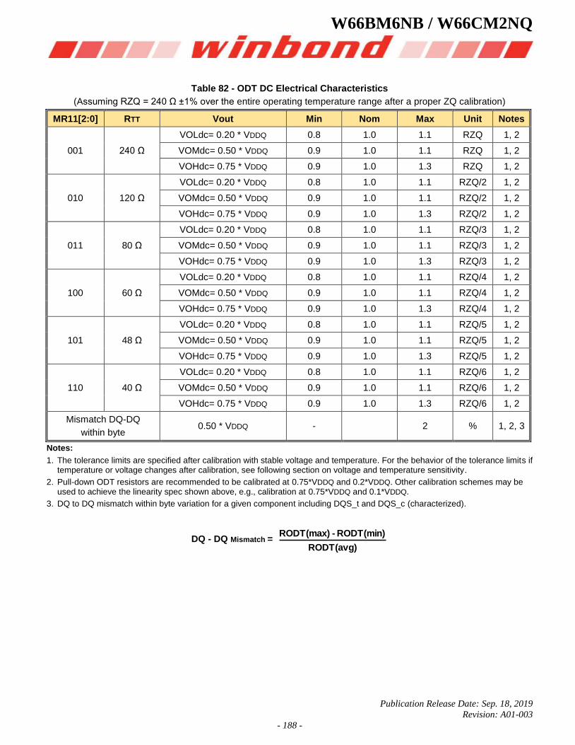
W66BM6NB / W66CM2NQ
Publication Release Date: Sep. 18, 2019
Revision: A01-003
- 188 -
Table 82 - ODT DC Electrical Characteristics
(Assuming RZQ = 240 Ω ±1% over the entire operating temperature range after a proper ZQ calibration)
MR11[2:0] RTT Vout Min Nom Max Unit Notes
001 240 Ω
VOLdc= 0.20 * VDDQ 0.8 1.0 1.1 RZQ 1, 2
VOMdc= 0.50 * VDDQ 0.9 1.0 1.1 RZQ 1, 2
VOHdc= 0.75 * VDDQ 0.9 1.0 1.3 RZQ 1, 2
010 120 Ω
VOLdc= 0.20 * VDDQ 0.8 1.0 1.1 RZQ/2 1, 2
VOMdc= 0.50 * VDDQ 0.9 1.0 1.1 RZQ/2 1, 2
VOHdc= 0.75 * VDDQ 0.9 1.0 1.3 RZQ/2 1, 2
011 80 Ω
VOLdc= 0.20 * VDDQ 0.8 1.0 1.1 RZQ/3 1, 2
VOMdc= 0.50 * VDDQ 0.9 1.0 1.1 RZQ/3 1, 2
VOHdc= 0.75 * VDDQ 0.9 1.0 1.3 RZQ/3 1, 2
100 60 Ω
VOLdc= 0.20 * VDDQ 0.8 1.0 1.1 RZQ/4 1, 2
VOMdc= 0.50 * VDDQ 0.9 1.0 1.1 RZQ/4 1, 2
VOHdc= 0.75 * VDDQ 0.9 1.0 1.3 RZQ/4 1, 2
101 48 Ω
VOLdc= 0.20 * VDDQ 0.8 1.0 1.1 RZQ/5 1, 2
VOMdc= 0.50 * VDDQ 0.9 1.0 1.1 RZQ/5 1, 2
VOHdc= 0.75 * VDDQ 0.9 1.0 1.3 RZQ/5 1, 2
110 40 Ω
VOLdc= 0.20 * VDDQ 0.8 1.0 1.1 RZQ/6 1, 2
VOMdc= 0.50 * VDDQ 0.9 1.0 1.1 RZQ/6 1, 2
VOHdc= 0.75 * VDDQ 0.9 1.0 1.3 RZQ/6 1, 2
Mismatch DQ-DQ
within byte 0.50 * VDDQ - 2 % 1, 2, 3
Notes:
1. The tolerance limits are specified after calibration with stable voltage and temperature. For the behavior of the tolerance limits if temperature or voltage changes after calibration, see following section on voltage and temperature sensitivity.
2. Pull-down ODT resistors are recommended to be calibrated at 0.75*VDDQ and 0.2*VDDQ. Other calibration schemes may be used to achieve the linearity spec shown above, e.g., calibration at 0.75*VDDQ and 0.1*VDDQ.
3. DQ to DQ mismatch within byte variation for a given component including DQS_t and DQS_c (characterized).
DQ - DQ Mismatch = RODT(avg)
RODT(min) - RODT(max)
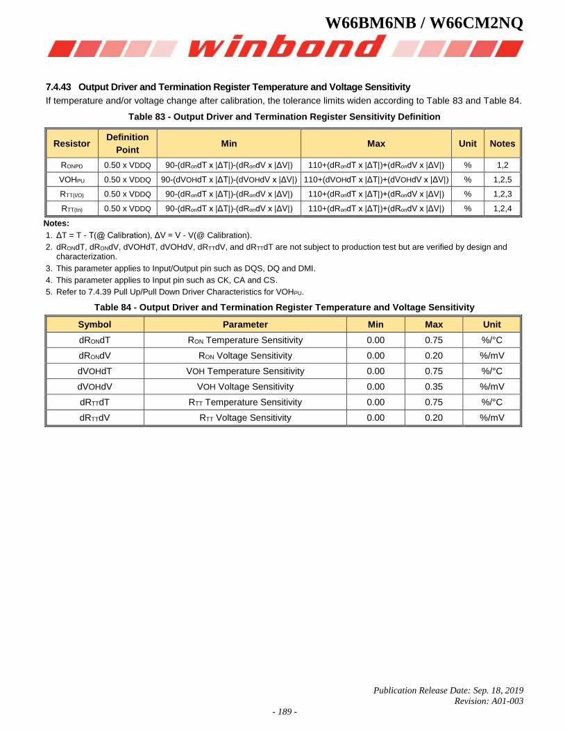
W66BM6NB / W66CM2NQ
Publication Release Date: Sep. 18, 2019
Revision: A01-003
- 189 -
7.4.43 Output Driver and Termination Register Temperature and Voltage Sensitivity
If temperature and/or voltage change after calibration, the tolerance limits widen according to Table 83 and Table 84.
Table 83 - Output Driver and Termination Register Sensitivity Definition
Resistor Definition
Point Min Max Unit Notes
RONPD 0.50 x VDDQ 90-(dRondT x |ΔT|)-(dRondV x |ΔV|) 110+(dRondT x |ΔT|)+(dRondV x |ΔV|) % 1,2
VOHPU 0.50 x VDDQ 90-(dVOHdT x |ΔT|)-(dVOHdV x |ΔV|) 110+(dVOHdT x |ΔT|)+(dVOHdV x |ΔV|) % 1,2,5
RTT(I/O) 0.50 x VDDQ 90-(dRondT x |ΔT|)-(dRondV x |ΔV|) 110+(dRondT x |ΔT|)+(dRondV x |ΔV|) % 1,2,3
RTT(In) 0.50 x VDDQ 90-(dRondT x |ΔT|)-(dRondV x |ΔV|) 110+(dRondT x |ΔT|)+(dRondV x |ΔV|) % 1,2,4
Notes:
1. ΔT = T - T(@ Calibration), ΔV = V - V(@ Calibration).
2. dRONdT, dRONdV, dVOHdT, dVOHdV, dRTTdV, and dRTTdT are not subject to production test but are verified by design and characterization.
3. This parameter applies to Input/Output pin such as DQS, DQ and DMI.
4. This parameter applies to Input pin such as CK, CA and CS.
5. Refer to 7.4.39 Pull Up/Pull Down Driver Characteristics for VOHPU.
Table 84 - Output Driver and Termination Register Temperature and Voltage Sensitivity
Symbol Parameter Min Max Unit
dRONdT RON Temperature Sensitivity 0.00 0.75 %/°C
dRONdV RON Voltage Sensitivity 0.00 0.20 %/mV
dVOHdT VOH Temperature Sensitivity 0.00 0.75 %/°C
dVOHdV VOH Voltage Sensitivity 0.00 0.35 %/mV
dRTTdT RTT Temperature Sensitivity 0.00 0.75 %/°C
dRTTdV RTT Voltage Sensitivity 0.00 0.20 %/mV
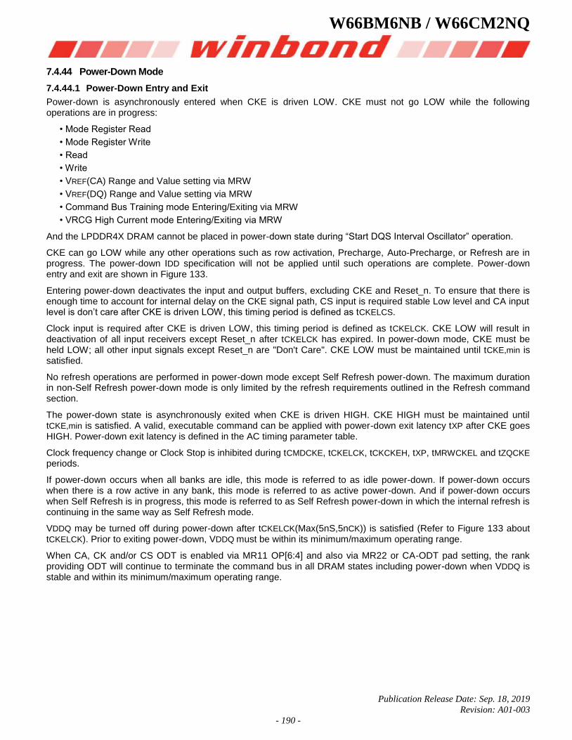
W66BM6NB / W66CM2NQ
Publication Release Date: Sep. 18, 2019
Revision: A01-003
- 190 -
7.4.44 Power-Down Mode
7.4.44.1 Power-Down Entry and Exit
Power-down is asynchronously entered when CKE is driven LOW. CKE must not go LOW while the following operations are in progress:
• Mode Register Read
• Mode Register Write
• Read
• Write
• VREF(CA) Range and Value setting via MRW
• VREF(DQ) Range and Value setting via MRW
• Command Bus Training mode Entering/Exiting via MRW
• VRCG High Current mode Entering/Exiting via MRW
And the LPDDR4X DRAM cannot be placed in power-down state during “Start DQS Interval Oscillator” operation.
CKE can go LOW while any other operations such as row activation, Precharge, Auto-Precharge, or Refresh are in progress. The power-down IDD specification will not be applied until such operations are complete. Power-down entry and exit are shown in Figure 133.
Entering power-down deactivates the input and output buffers, excluding CKE and Reset_n. To ensure that there is enough time to account for internal delay on the CKE signal path, CS input is required stable Low level and CA input level is don’t care after CKE is driven LOW, this timing period is defined as tCKELCS.
Clock input is required after CKE is driven LOW, this timing period is defined as tCKELCK. CKE LOW will result in deactivation of all input receivers except Reset_n after tCKELCK has expired. In power-down mode, CKE must be held LOW; all other input signals except Reset_n are "Don't Care". CKE LOW must be maintained until tCKE,min is satisfied.
No refresh operations are performed in power-down mode except Self Refresh power-down. The maximum duration in non-Self Refresh power-down mode is only limited by the refresh requirements outlined in the Refresh command section.
The power-down state is asynchronously exited when CKE is driven HIGH. CKE HIGH must be maintained until tCKE,min is satisfied. A valid, executable command can be applied with power-down exit latency tXP after CKE goes HIGH. Power-down exit latency is defined in the AC timing parameter table.
Clock frequency change or Clock Stop is inhibited during tCMDCKE, tCKELCK, tCKCKEH, tXP, tMRWCKEL and tZQCKE periods.
If power-down occurs when all banks are idle, this mode is referred to as idle power-down. If power-down occurs when there is a row active in any bank, this mode is referred to as active power-down. And if power-down occurs when Self Refresh is in progress, this mode is referred to as Self Refresh power-down in which the internal refresh is continuing in the same way as Self Refresh mode.
VDDQ may be turned off during power-down after tCKELCK(Max(5nS,5nCK)) is satisfied (Refer to Figure 133 about tCKELCK). Prior to exiting power-down, VDDQ must be within its minimum/maximum operating range.
When CA, CK and/or CS ODT is enabled via MR11 OP[6:4] and also via MR22 or CA-ODT pad setting, the rank providing ODT will continue to terminate the command bus in all DRAM states including power-down when VDDQ is stable and within its minimum/maximum operating range.
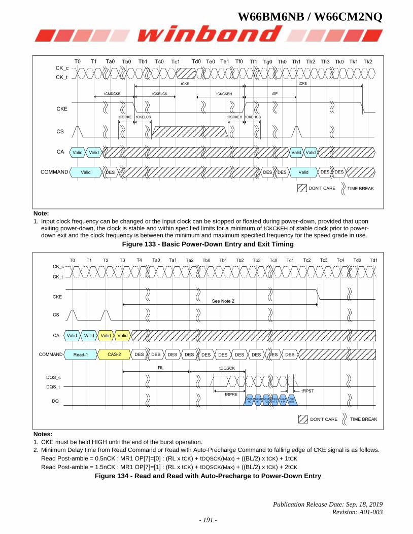
W66BM6NB / W66CM2NQ
Publication Release Date: Sep. 18, 2019
Revision: A01-003
- 191 -
TIME BREAKDON'T CARE
tCMDCKE tCKELCK tCKCKEH
tCKE
tXP
tCKE
tCSCKEH tCKEHCStCSCKE tCKELCS
CK_c
CK_t
COMMAND
CA
CS
CKE
T0 T1 Ta0 Tb0 Tb1 Tc0 Tc1 Td0 Te0 Te1 Tf0 Tf1 Tg0 Th0 Th1 Th2 Th3 Tk0 Tk1 Tk2
Valid Valid
Valid DES
Valid Valid
ValidDES DES DES DES
Note:
1. Input clock frequency can be changed or the input clock can be stopped or floated during power-down, provided that upon exiting power-down, the clock is stable and within specified limits for a minimum of tCKCKEH of stable clock prior to power-down exit and the clock frequency is between the minimum and maximum specified frequency for the speed grade in use.
Figure 133 - Basic Power-Down Entry and Exit Timing
CK_c
CK_t
T0 T1 T2 T3 T4 Ta0 Ta1 Ta2 Tb0 Tb1 Tb2 Tb3 Tc0 Tc1 Tc2 Tc3 Tc4 Td0 Td1
Read-1 CAS-2
Valid ValidValid
tRPSTtRPRE
RL
DES DES DES DES DES DESDES DES DES DESCOMMAND
CS
CA
DQS_c
DQS_t
DQDout n14
Dout n15
Dout n2
Dout n13
Dout n0
Dout n1
DON'T CARE TIME BREAK
CKE
Valid
tDQSCK
See Note 2
Notes:
1. CKE must be held HIGH until the end of the burst operation.
2. Minimum Delay time from Read Command or Read with Auto-Precharge Command to falling edge of CKE signal is as follows.
Read Post-amble = 0.5nCK : MR1 OP[7]=[0] : (RL x tCK) + tDQSCK(Max) + ((BL/2) x tCK) + 1tCK
Read Post-amble = 1.5nCK : MR1 OP[7]=[1] : (RL x tCK) + tDQSCK(Max) + ((BL/2) x tCK) + 2tCK
Figure 134 - Read and Read with Auto-Precharge to Power-Down Entry
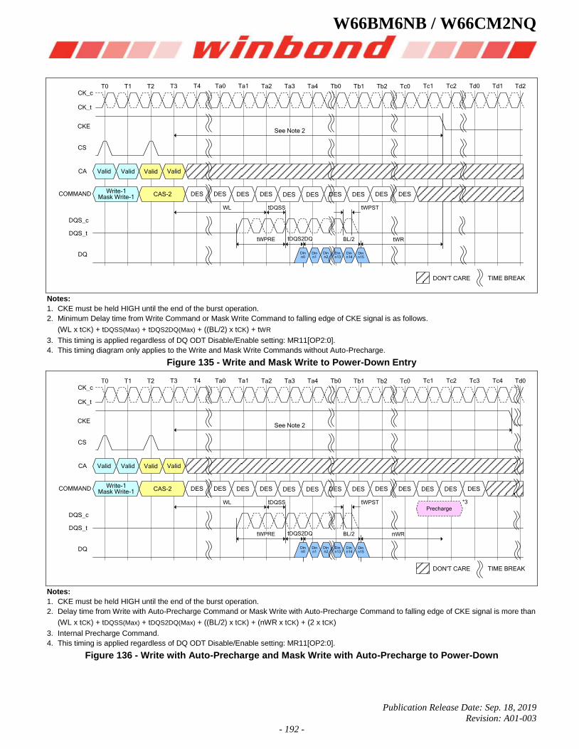
W66BM6NB / W66CM2NQ
Publication Release Date: Sep. 18, 2019
Revision: A01-003
- 192 -
CK_c
CK_t
T0 T1 T2 T3 T4 Ta0 Ta1 Ta2 Ta3 Ta4 Tb0 Tb1 Tb2 Tc0 Tc1 Tc2 Td0 Td1 Td2
Write-1CAS-2
Valid ValidValid
tWPST
tWPRE
WL
DES DES DES DES DES DESDES DES DES DESCOMMAND
CS
CA
DQS_c
DQS_t
DQ Din n14
Din n15
Din n2
Din n13
Din n0
Din n1
DON'T CARE TIME BREAK
CKE
Valid
tDQSS
See Note 2
Mask Write-1
tDQS2DQ BL/2 tWR
Notes:
1. CKE must be held HIGH until the end of the burst operation.
2. Minimum Delay time from Write Command or Mask Write Command to falling edge of CKE signal is as follows.
(WL x tCK) + tDQSS(Max) + tDQS2DQ(Max) + ((BL/2) x tCK) + tWR
3. This timing is applied regardless of DQ ODT Disable/Enable setting: MR11[OP2:0].
4. This timing diagram only applies to the Write and Mask Write Commands without Auto-Precharge.
Figure 135 - Write and Mask Write to Power-Down Entry
CK_c
CK_t
T0 T1 T2 T3 T4 Ta0 Ta1 Ta2 Ta3 Ta4 Tb0 Tb1 Tb2 Tc0 Tc1 Tc2 Tc3 Tc4 Td0
Write-1CAS-2
Valid ValidValid
tWPST
tWPRE
WL
DES DES DES DES DES DESDES DES DES DESCOMMAND
CS
CA
DQS_c
DQS_t
DQ Din n14
Din n15
Din n2
Din n13
Din n0
Din n1
DON'T CARE TIME BREAK
CKE
Valid
tDQSS
See Note 2
Mask Write-1
tDQS2DQ BL/2 nWR
DES DES DES
Precharge
*3
Notes:
1. CKE must be held HIGH until the end of the burst operation.
2. Delay time from Write with Auto-Precharge Command or Mask Write with Auto-Precharge Command to falling edge of CKE signal is more than
(WL x tCK) + tDQSS(Max) + tDQS2DQ(Max) + ((BL/2) x tCK) + (nWR x tCK) + (2 x tCK)
3. Internal Precharge Command.
4. This timing is applied regardless of DQ ODT Disable/Enable setting: MR11[OP2:0].
Figure 136 - Write with Auto-Precharge and Mask Write with Auto-Precharge to Power-Down
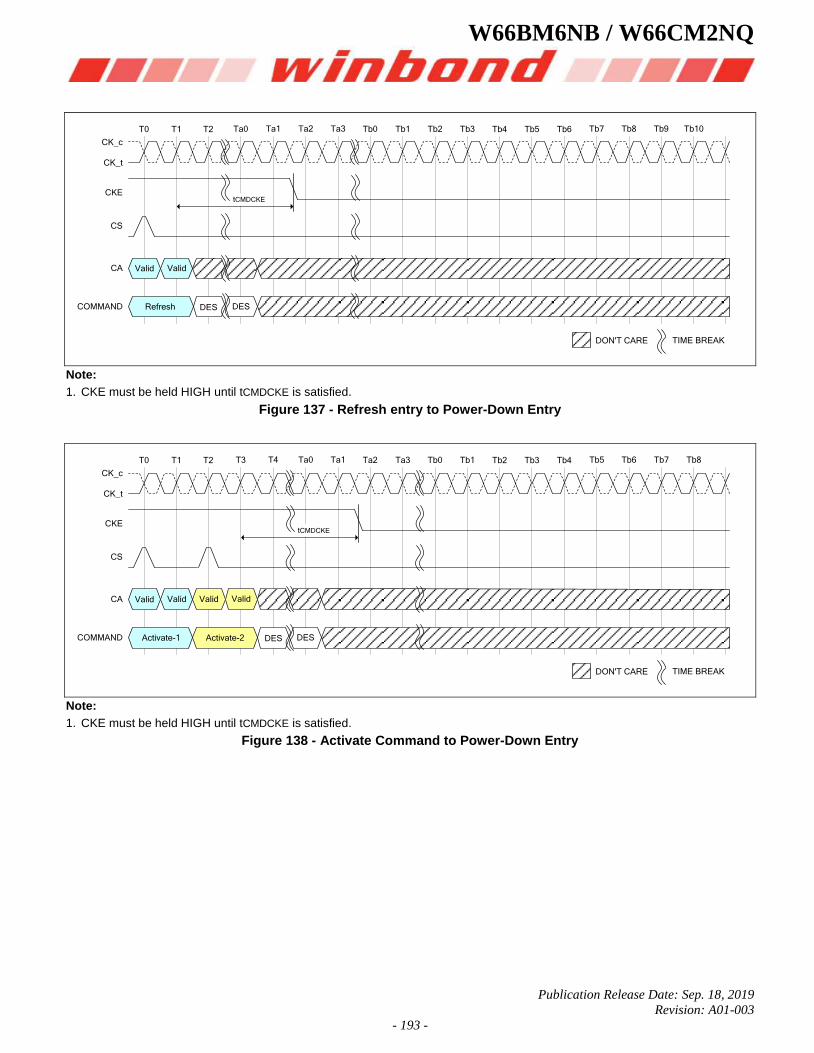
W66BM6NB / W66CM2NQ
Publication Release Date: Sep. 18, 2019
Revision: A01-003
- 193 -
CK_c
CK_t
COMMAND
T0 T1 T2 Ta0 Ta1 Ta2 Ta3 Tb0 Tb1 Tb2 Tb3 Tb4 Tb5 Tb6 Tb7 Tb8 Tb9 Tb10
CA
CS
DES
CKE
Valid
tCMDCKE
Valid
DESRefresh
DON'T CARE TIME BREAK
Note:
1. CKE must be held HIGH until tCMDCKE is satisfied.
Figure 137 - Refresh entry to Power-Down Entry
CK_c
CK_t
COMMAND
T0 T1 T2 T3 T4 Ta0 Ta1 Ta2 Ta3 Tb0 Tb1 Tb2 Tb3 Tb4 Tb5 Tb6 Tb7 Tb8
CA
CS
DES
CKE
Valid
tCMDCKE
Valid
DESActivate-1
DON'T CARE TIME BREAK
Valid Valid
Activate-2
Note:
1. CKE must be held HIGH until tCMDCKE is satisfied.
Figure 138 - Activate Command to Power-Down Entry
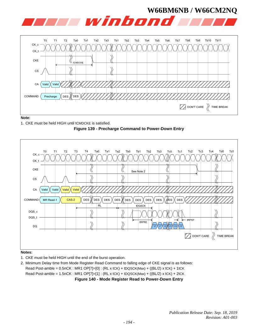
W66BM6NB / W66CM2NQ
Publication Release Date: Sep. 18, 2019
Revision: A01-003
- 194 -
CK_c
CK_t
COMMAND
T0 T1 T2 Ta0 Ta1 Ta2 Ta3 Tb1 Tb2 Tb3 Tb4 Tb5 Tb6 Tb7 Tb8 Tb9 Tb10 Tb11
CA
CS
DES
CKE
Valid
tCMDCKE
Valid
DESPrecharge
DON'T CARE TIME BREAK
Note:
1. CKE must be held HIGH until tCMDCKE is satisfied.
Figure 139 - Precharge Command to Power-Down Entry
CK_c
CK_t
T0 T1 T2 T3 T4 Ta0 Ta1 Ta2 Tb0 Tb1 Tb2 Tb3 Tc0 Tc1 Tc2 Tc3 Tc4 Td0 Td1
MR Read-1 CAS-2
Valid ValidValid
tRPSTtRPRE
RL
DES DES DES DES DES DESDES DES DES DESCOMMAND
CS
CA
DQS_c
DQS_t
DQDout n14
Dout n15
Dout n2
Dout n13
Dout n0
Dout n1
DON'T CARE TIME BREAK
CKE
Valid
tDQSCK
See Note 2
Notes:
1. CKE must be held HIGH until the end of the burst operation.
2. Minimum Delay time from Mode Register Read Command to falling edge of CKE signal is as follows:
Read Post-amble = 0.5nCK : MR1 OP[7]=[0] : (RL x tCK) + tDQSCK(Max) + ((BL/2) x tCK) + 1tCK
Read Post-amble = 1.5nCK : MR1 OP[7]=[1] : (RL x tCK) + tDQSCK(Max) + ((BL/2) x tCK) + 2tCK
Figure 140 - Mode Register Read to Power-Down Entry
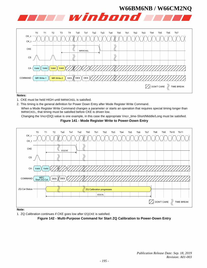
W66BM6NB / W66CM2NQ
Publication Release Date: Sep. 18, 2019
Revision: A01-003
- 195 -
CK_c
CK_t
COMMAND
T0 T1 T2 T3 T4 Ta0 Ta1 Ta2 Ta3 Ta4 Tb0 Tb1 Tb2 Tb3 Tb4 Tb5 Tb6 Tb7
CA
CS
DES
CKE
Valid
tMRWCKEL
Valid
DESMR Write-1
DON'T CARE TIME BREAK
Valid Valid
MR Write-2 DES
Notes:
1. CKE must be held HIGH until tMRWCKEL is satisfied.
2. This timing is the general definition for Power Down Entry after Mode Register Write Command.
When a Mode Register Write Command changes a parameter or starts an operation that requires special timing longer than tMRWCKEL, that timing must be satisfied before CKE is driven low.
Changing the VREF(DQ) value is one example, in this case the appropriate VREF_time-Short/Middle/Long must be satisfied.
Figure 141 - Mode Register Write to Power-Down Entry
CK_c
CK_t
COMMAND
T0 T1 T2 Ta0 Ta1 Ta2 Tb0 Tb1 Tb2 Tb3 Tb4 Tb5 Tb6 Tb7 Tb8 Tb9 Tb10 Tb11
CA
CS
DES
CKE
Valid
tZQCKE
Valid
DESStart ZQ Cal
DON'T CARE TIME BREAK
MPC
ZQ Calibration progresses
tZQCAL
ZQ Cal Status
Note:
1. ZQ Calibration continues if CKE goes low after tZQCKE is satisfied.
Figure 142 - Multi-Purpose Command for Start ZQ Calibration to Power-Down Entry
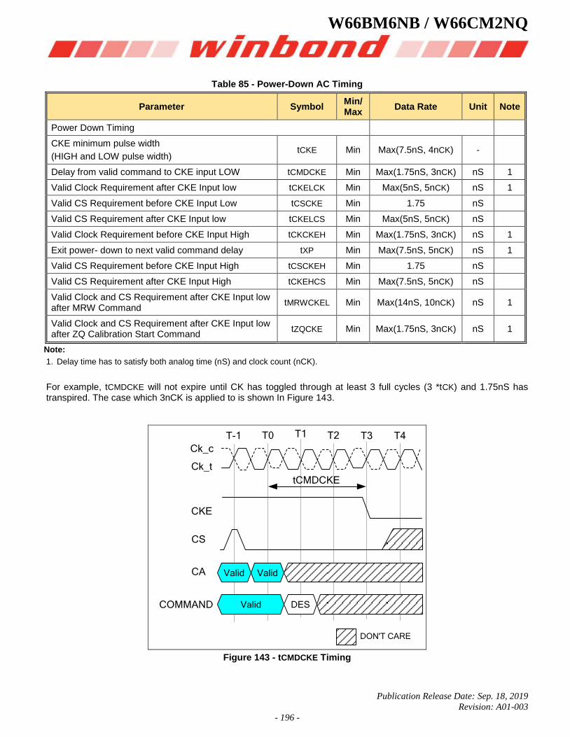
W66BM6NB / W66CM2NQ
Publication Release Date: Sep. 18, 2019
Revision: A01-003
- 196 -
Table 85 - Power-Down AC Timing
Parameter Symbol Min/ Max
Data Rate Unit Note
Power Down Timing
CKE minimum pulse width
(HIGH and LOW pulse width) tCKE Min Max(7.5nS, 4nCK) -
Delay from valid command to CKE input LOW tCMDCKE Min Max(1.75nS, 3nCK) nS 1
Valid Clock Requirement after CKE Input low tCKELCK Min Max(5nS, 5nCK) nS 1
Valid CS Requirement before CKE Input Low tCSCKE Min 1.75 nS
Valid CS Requirement after CKE Input low tCKELCS Min Max(5nS, 5nCK) nS
Valid Clock Requirement before CKE Input High tCKCKEH Min Max(1.75nS, 3nCK) nS 1
Exit power- down to next valid command delay tXP Min Max(7.5nS, 5nCK) nS 1
Valid CS Requirement before CKE Input High tCSCKEH Min 1.75 nS
Valid CS Requirement after CKE Input High tCKEHCS Min Max(7.5nS, 5nCK) nS
Valid Clock and CS Requirement after CKE Input low after MRW Command
tMRWCKEL Min Max(14nS, 10nCK) nS 1
Valid Clock and CS Requirement after CKE Input low after ZQ Calibration Start Command
tZQCKE Min Max(1.75nS, 3nCK) nS 1
Note:
1. Delay time has to satisfy both analog time (nS) and clock count (nCK).
For example, tCMDCKE will not expire until CK has toggled through at least 3 full cycles (3 *tCK) and 1.75nS has transpired. The case which 3nCK is applied to is shown In Figure 143.
T-1 T4
DON'T CARE
COMMAND
T3
T2T1T0
CA
CS
CKE
Ck_t
Ck_c
tCMDCKE
DESValid
Valid Valid
Figure 143 - tCMDCKE Timing

W66BM6NB / W66CM2NQ
Publication Release Date: Sep. 18, 2019
Revision: A01-003
- 197 -
7.4.45 Input Clock Stop and Frequency Change
LPDDR4X SDRAMs support input clock frequency change during CKE LOW under the following conditions:
• tCK(abs)min is met for each clock cycle;
• Refresh requirements apply during clock frequency change;
• During clock frequency change, only REFab or REFpb commands may be executing;
• Any Activate or Precharge commands have executed to completion prior to changing the frequency;
• The related timing conditions (tRCD, tRP) have been met prior to changing the frequency;
• The initial clock frequency shall be maintained for a minimum of tCKELCK after CKE goes LOW;
• The clock satisfies tCH(abs) and tCL(abs) for a minimum of tCKCKEH prior to CKE going HIGH
After the input clock frequency is changed and CKE is held HIGH, additional MRW commands may be required to set the WR, RL etc. These settings may need to be adjusted to meet minimum timing requirements at the target clock frequency.
LPDDR4X devices support clock stop during CKE LOW under the following conditions:
• CK_t and CK_c are don’t care during clock stop;
• Refresh requirements apply during clock stop;
• During clock stop, only REFab or REFpb commands may be executing;
• Any Activate or Precharge commands have executed to completion prior to stopping the clock;
• The related timing conditions (tRCD, tRP) have been met prior to stopping the clock;
• The initial clock frequency shall be maintained for a minimum of tCKELCK after CKE goes LOW;
• The clock satisfies tCH(abs) and tCL(abs) for a minimum of tCKCKEH prior to CKE going HIGH
LPDDR4X devices support input clock frequency change during CKE HIGH under the following conditions:
• tCK(abs)min is met for each clock cycle;
• Refresh requirements apply during clock frequency change;
• Any Activate, Read, Write, Precharge, Mode Register Write, or Mode Register Read commands must have executed to completion, including any associated data bursts prior to changing the frequency;
• The related timing conditions (tRCD, tWR, tWRA, tRP, tMRW, tMRR, etc.) have been met prior to changing the frequency;
• CS shall be held LOW during clock frequency change;
• During clock frequency change, only REFab or REFpb commands may be executing;
• The LPDDR4X SDRAM is ready for normal operation after the clock satisfies tCH(abs) and tCL(abs) for a minimum of 2*tCK+tXP.
After the input clock frequency is changed, additional MRW commands may be required to set the WR, RL etc. These settings may need to be adjusted to meet minimum timing requirements at the target clock frequency.
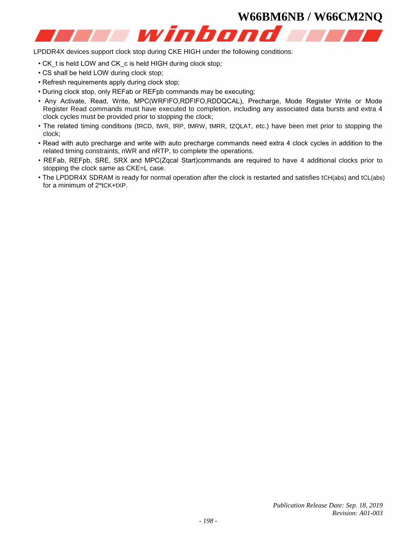
W66BM6NB / W66CM2NQ
Publication Release Date: Sep. 18, 2019
Revision: A01-003
- 198 -
LPDDR4X devices support clock stop during CKE HIGH under the following conditions:
• CK_t is held LOW and CK_c is held HIGH during clock stop;
• CS shall be held LOW during clock stop;
• Refresh requirements apply during clock stop;
• During clock stop, only REFab or REFpb commands may be executing;
• Any Activate, Read, Write, MPC(WRFIFO,RDFIFO,RDDQCAL), Precharge, Mode Register Write or Mode Register Read commands must have executed to completion, including any associated data bursts and extra 4 clock cycles must be provided prior to stopping the clock;
• The related timing conditions (tRCD, tWR, tRP, tMRW, tMRR, tZQLAT, etc.) have been met prior to stopping the clock;
• Read with auto precharge and write with auto precharge commands need extra 4 clock cycles in addition to the related timing constraints, nWR and nRTP, to complete the operations.
• REFab, REFpb, SRE, SRX and MPC(Zqcal Start)commands are required to have 4 additional clocks prior to stopping the clock same as CKE=L case.
• The LPDDR4X SDRAM is ready for normal operation after the clock is restarted and satisfies tCH(abs) and tCL(abs) for a minimum of 2*tCK+tXP.
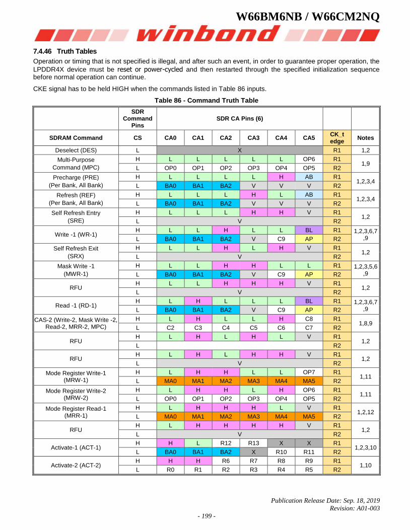
W66BM6NB / W66CM2NQ
Publication Release Date: Sep. 18, 2019
Revision: A01-003
- 199 -
7.4.46 Truth Tables
Operation or timing that is not specified is illegal, and after such an event, in order to guarantee proper operation, the
LPDDR4X device must be reset or power-cycled and then restarted through the specified initialization sequence before normal operation can continue.
CKE signal has to be held HIGH when the commands listed in Table 86 inputs.
Table 86 - Command Truth Table
SDR
Command Pins
SDR CA Pins (6)
SDRAM Command CS CA0 CA1 CA2 CA3 CA4 CA5 CK_t edge
Notes
Deselect (DES) L X R1 1,2
Multi-Purpose
Command (MPC)
H L L L L L OP6 R1 1,9
L OP0 OP1 OP2 OP3 OP4 OP5 R2
Precharge (PRE)
(Per Bank, All Bank)
H L L L L H AB R1 1,2,3,4
L BA0 BA1 BA2 V V V R2
Refresh (REF)
(Per Bank, All Bank)
H L L L H L AB R1 1,2,3,4
L BA0 BA1 BA2 V V V R2
Self Refresh Entry
(SRE)
H L L L H H V R1 1,2
L V R2
Write -1 (WR-1) H L L H L L BL R1 1,2,3,6,7
,9 L BA0 BA1 BA2 V C9 AP R2
Self Refresh Exit
(SRX)
H L L H L H V R1 1,2
L V R2
Mask Write -1
(MWR-1)
H L L H H L L R1 1,2,3,5,6,9 L BA0 BA1 BA2 V C9 AP R2
RFU H L L H H H V R1
1,2 L V R2
Read -1 (RD-1) H L H L L L BL R1 1,2,3,6,7
,9 L BA0 BA1 BA2 V C9 AP R2
CAS-2 (Write-2, Mask Write -2, Read-2, MRR-2, MPC)
H L H L L H C8 R1 1,8,9
L C2 C3 C4 C5 C6 C7 R2
RFU H L H L H L V R1
1,2 L R2
RFU H L H L H H V R1
1,2 L V R2
Mode Register Write-1 (MRW-1)
H L H H L L OP7 R1 1,11
L MA0 MA1 MA2 MA3 MA4 MA5 R2
Mode Register Write-2 (MRW-2)
H L H H L H OP6 R1 1,11
L OP0 OP1 OP2 OP3 OP4 OP5 R2
Mode Register Read-1 (MRR-1)
H L H H H L V R1 1,2,12
L MA0 MA1 MA2 MA3 MA4 MA5 R2
RFU H L H H H H V R1
1,2 L V R2
Activate-1 (ACT-1) H H L R12 R13 X X R1
1,2,3,10 L BA0 BA1 BA2 X R10 R11 R2
Activate-2 (ACT-2) H H H R6 R7 R8 R9 R1
1,10 L R0 R1 R2 R3 R4 R5 R2
W66BM6NB / W66CM2NQ
Publication Release Date: Sep. 18, 2019
Revision: A01-003
- 200 -
Notes:
1. All LPDDR4X commands except for Deselect are 2 clock cycle long and defined by states of CS and CA[5:0] at the first rising edge of clock. Deselect command is 1 clock cycle long.
2. "V" means "H" or "L" (a defined logic level). "X" means don’t care in which case CA[5:0] can be floated.
3. Bank addresses BA[2:0] determine which bank is to be operated upon.
4. AB "HIGH" during Precharge or Refresh command indicates that command must be applied to all banks and bank address are don’t care.
5. Mask Write-1 command supports only BL 16. For Mark Write-1 command, CA5 must be driven LOW on first rising clock cycle (R1).
6. AP "HIGH" during Write-1, Mask Write-1 or Read-1 commands indicates that an Auto-Precharge will occur to the bank associated with the Write, Mask Write or Read command.
7. If Burst Length on-the-fly is enabled, BL "HIGH" during Write-1 or Read-1 command indicates that Burst Length should be set on-the-Fly to BL=32. BL "LOW" during Write-1 or Read-1 command indicates that Burst Length should be set on-the-fly to BL=16. If Burst Length on-the-fly is disabled, then BL must be driven to defined logic level "H" or "L".
8. For CAS-2 commands (Write-2 or Mask Write-2 or Read-2 or MRR-2 or MPC (Only Write FIFO, Read FIFO & Read DQ Calibration), C[1:0] are not transmitted on the CA[5:0] bus and are assumed to be zero. Note that for CAS-2 Write-2 or CAS-2 Mask Write-2 command, C[3:2] must be driven LOW.
9. Write-1 or Mask Write-1 or Read-1 or Mode Register Read-1 or MPC (Only Write FIFO, Read FIFO & Read DQ Calibration) command must be immediately followed by CAS-2 command consecutively without any other command in between. Write-1 or Mask Write-1 or Read-1 or Mode Register Read-1 or MPC (Only Write FIFO, Read FIFO & Read DQ Calibration) command must be issued first before issuing CAS-2 command. MPC (Only Start & Stop DQS Oscillator, Start & Latch ZQ Calibration) commands do not require CAS-2 command; they require two additional DES or NOP commands consecutively before issuing any other commands.
10. Activate-1 command must be immediately followed by Activate-2 command consecutively without any other command in between. Activate-1 command must be issued first before issuing Activate-2 command. Once
11. MRW-1 command must be immediately followed by MRW-2 command consecutively without any other command in between. MRW-1 command must be issued first before issuing MRW-2 command.
12. MRR-1 command must be immediately followed by CAS-2 command consecutively without any other command in between. MRR-1 command must be issued first before issuing CAS-2 command.
W66BM6NB / W66CM2NQ
Publication Release Date: Sep. 18, 2019
Revision: A01-003
- 201 -
7.4.47 TRR Mode - Target Row Refresh
A LPDDR4X SDRAM's row has a limited number of times a given row can be accessed within a refresh period (tREFW * 2) prior to requiring adjacent rows to be refreshed. The Maximum Activate Count (MAC) is the maximum number of activates that a single row can sustain within a refresh period before the adjacent rows need to be refreshed. The row receiving the excessive actives is the Target Row (TRn), the adjacent rows to be refreshed are the victim rows. When the MAC limit is reached on TRn, either the LPDDR4X SDRAM receive all (R * 2) Refresh Commands before another row activate is issued, or the LPDDR4X SDRAM should be placed into Targeted Row Refresh (TRR) mode. The TRR Mode will re-fresh the rows adjacent to the TRn that encountered tMAC limit.
There could be a maximum of two target rows to a victim row in a bank. The cumulative value of the activation from the two target rows on a victim row in a bank should not exceed MAC value as well. MR24 fields required to support the new TRR settings. Setting MR24 [OP7=1] enables TRR Mode and setting MR24 [OP7=0] disables TRR Mode. MR24 [OP6:OP4] defines which bank (BAn) the target row is located in (See MR24 table for details).
The TRR mode must be disabled during initialization as well as any other LPDDR4X SDRAM calibration modes. The TRR mode is entered from a DRAM Idle State, once TRR mode has been entered, no other Mode Register commands are allowed until TRR mode is completed, except setting MR24 [OP7=0] to interrupt and reissue the TRR mode is allowed.
When enabled; TRR Mode is self-clearing; the mode will be disabled automatically after the completion of defined TRR flow; after the 3rd BAn precharge has completed plus tMRD. The TRR mode can also be exited via another MRS command at the completion of TRR by setting MR24 [OP7=0]; if the TRR is exited via another MRS command, the value written to MR24 [OP6:OP4] are don’t cares.
7.4.47.1 TRR Mode Operation
1. The timing diagram in Figure 148 depicts TRR mode. The following steps must be performed when TRR mode is enabled. This mode requires all three ACT (ACT1, ACT2 and ACT3) and three corresponding PRE commands (PRE1, PRE2 and PRE3) to complete TRR mode. A Precharge All (PREA) commands issued while LPDDR4X SDRAM is in TRR mode will also perform precharge to BAn and counts towards a PREn command.
2. Prior to issuing the MRW command to enter TRR mode, the SDRAM should be in the idle state. A MRW command must be issued with MR24 [OP7=1] and MR24 [OP6:4] defining the bank in which the targeted row is located. All other MR24 bits should remain unchanged.
3. No activity is to occur in the DRAM until tMRD has been satisfied. Once tMRD has been satisfied, the only commands to BAn allowed are ACT and PRE until the TRR mode has been completed.
4. The first ACT to the BAn with the TRn address can now be applied, no other command is allowed at this point. All other banks must remain inactive from when the first BAn ACT command is issued until [(1.5 *tRAS) + tRP] is satisfied.
5. After the first ACT to the BAn with the TRn address is issued, a PRE to BAn is to be issued (1.5 * tRAS) later; and then followed tRP later by the second ACT to the BAn with the TRn address. Once the 2nd activate to the BAn is issued, non BAn banks are allowed to have activity.
6. After the second ACT to the BAn with the TRn address is issued, a PRE to BAn is to be issued tRAS later and then followed tRP later by the third ACT to the BAn with the TRn address.
7. After the third ACT to the BAn with the TRn address is issued, a PRE to BAn would be issued tRAS later; and once the third PRE has been issued, non BAn banks are not allowed to have activity until TRR mode is exited. The TRR mode is completed once tRP plus tMRD is satisfied.
8. TRR mode must be completed as specified to guarantee that adjacent rows are refreshed. Any-time the TRR mode is interrupted and not completed; the interrupted TRR Mode must be cleared and then subsequently performed again. To clear an interrupted TRR mode, an MR24 change is required with setting MR24 [OP7=0], MR24 [OP6:4] are don’t care, followed by three PRE to BAn, tRP time in between each PRE command. The complete TRR sequence (Steps 2-7) must be then re-issued and completed to guarantee that the adjacent rows are refreshed.
9. Refresh command to the LPDDR4X SDRAM or entering Self Refresh mode is not allowed while the DRAM is in TRR mode.
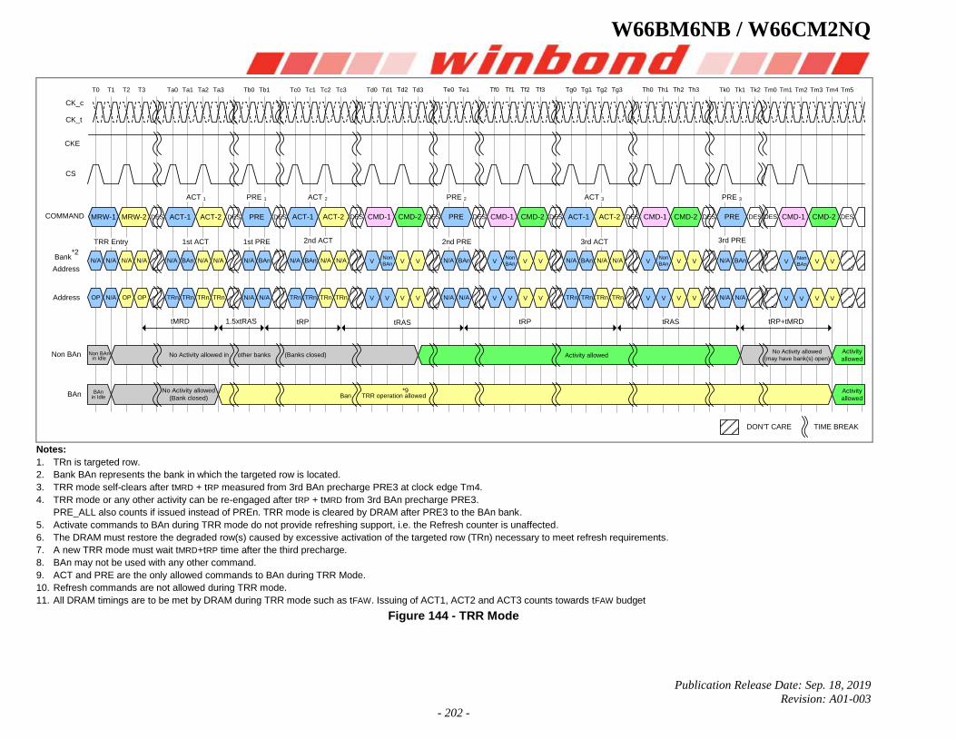
W66BM6NB / W66CM2NQ
Publication Release Date: Sep. 18, 2019
Revision: A01-003
- 202 -
T0 T1 T2 T3 Ta1 Ta2 Ta3 Tb0Ta0 Tb1
COMMAND
Tc1 Tc2 Tc3Tc0 Td1 Td2 Td3Td0 Te0 Te1 Tf1 Tf2 Tf3Tf0 Tg1 Tg2 Tg3Tg0 Th1 Th2 Th3Th0 Tk1 Tk2 Tm0Tk0 Tm2 Tm3 Tm4Tm1 Tm5
MRW-1 DESMRW-2 ACT-1 DESACT-2 DESPRE ACT-1 DESACT-2 CMD-1 DESCMD-2 DESPRE CMD-1 DESCMD-2 ACT-1 DESACT-2 CMD-1 DESCMD-2 DESPRE DES CMD-1 DESCMD-2
N/A N/A N/A N/A N/A BAn N/A N/A N/A BAn N/A BAn N/A N/A VNon
BAn V V N/A BAn VNon
BAn V V N/A BAn N/A N/A VNon
BAn V V N/A BAn VNon
BAn V V
OP N/A OP OP TRn TRn TRn TRn N/A N/A V V V N/A N/A V V V V V V N/A N/A V V VTRn TRn TRn TRn V V TRn TRn TRn TRn V V
Non BAnin Idle
No Activity allowed in other banks (Banks closed) Activity allowedNo Activity allowed
(may have bank(s) open)
Activity
allowed
BAnin Idle
No Activity allowed
(Bank closed) Ban TRR operation allowed*9 Activity
allowed
TIME BREAKDON'T CARE
ACT 1 PRE 1 ACT 2 PRE 2 ACT 3 PRE 3
TRR Entry 1st ACT 1st PRE 2nd ACT 2nd PRE 3rd ACT 3rd PRE
tMRD tRP1.5xtRAS tRAS tRP tRAS tRP+tMRD
CK_c
CK_t
CKE
CS
Bank
Address
Non BAn
Address
BAn
*2
Notes:
1. TRn is targeted row.
2. Bank BAn represents the bank in which the targeted row is located.
3. TRR mode self-clears after tMRD + tRP measured from 3rd BAn precharge PRE3 at clock edge Tm4.
4. TRR mode or any other activity can be re-engaged after tRP + tMRD from 3rd BAn precharge PRE3.
PRE_ALL also counts if issued instead of PREn. TRR mode is cleared by DRAM after PRE3 to the BAn bank.
5. Activate commands to BAn during TRR mode do not provide refreshing support, i.e. the Refresh counter is unaffected.
6. The DRAM must restore the degraded row(s) caused by excessive activation of the targeted row (TRn) necessary to meet refresh requirements.
7. A new TRR mode must wait tMRD+tRP time after the third precharge.
8. BAn may not be used with any other command.
9. ACT and PRE are the only allowed commands to BAn during TRR Mode.
10. Refresh commands are not allowed during TRR mode.
11. All DRAM timings are to be met by DRAM during TRR mode such as tFAW. Issuing of ACT1, ACT2 and ACT3 counts towards tFAW budget
Figure 144 - TRR Mode
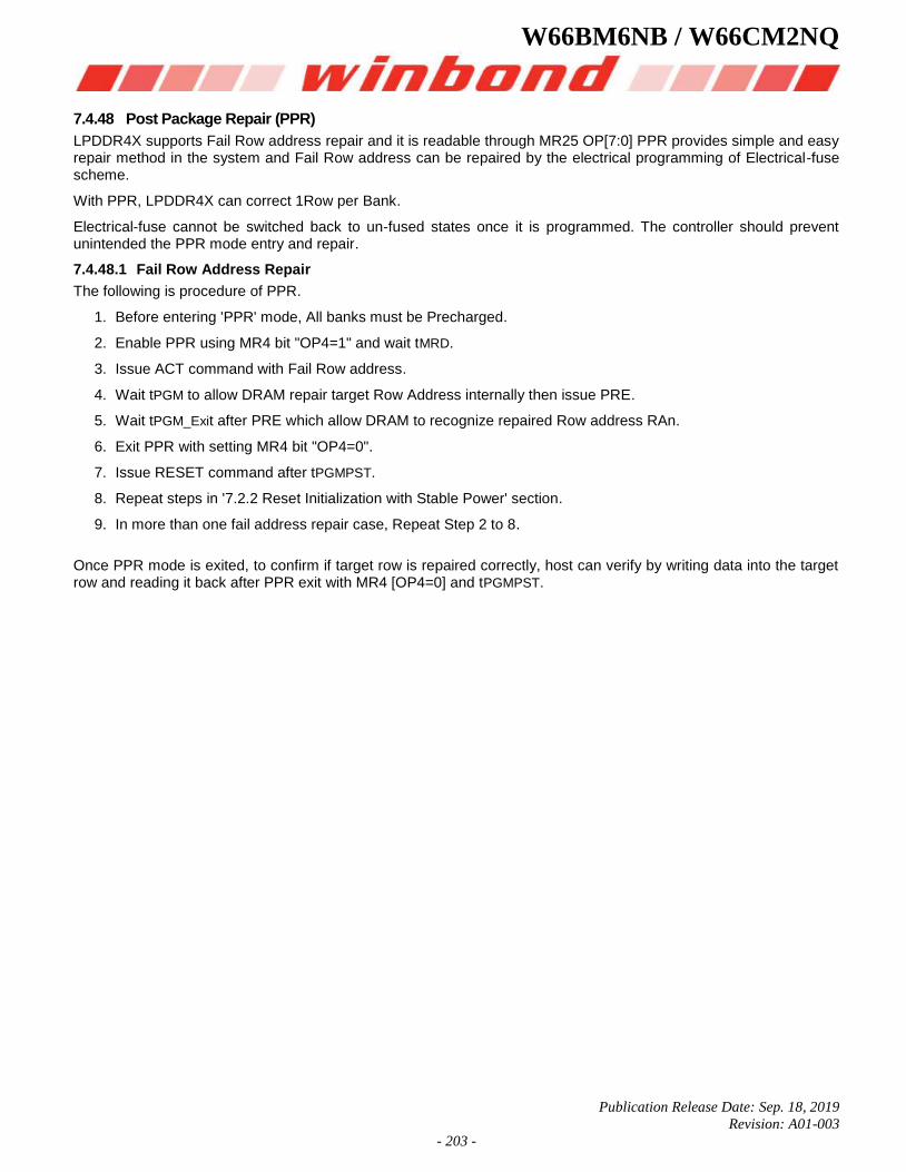
W66BM6NB / W66CM2NQ
Publication Release Date: Sep. 18, 2019
Revision: A01-003
- 203 -
7.4.48 Post Package Repair (PPR)
LPDDR4X supports Fail Row address repair and it is readable through MR25 OP[7:0] PPR provides simple and easy repair method in the system and Fail Row address can be repaired by the electrical programming of Electrical-fuse scheme.
With PPR, LPDDR4X can correct 1Row per Bank.
Electrical-fuse cannot be switched back to un-fused states once it is programmed. The controller should prevent unintended the PPR mode entry and repair.
7.4.48.1 Fail Row Address Repair
The following is procedure of PPR.
1. Before entering 'PPR' mode, All banks must be Precharged.
2. Enable PPR using MR4 bit "OP4=1" and wait tMRD.
3. Issue ACT command with Fail Row address.
4. Wait tPGM to allow DRAM repair target Row Address internally then issue PRE.
5. Wait tPGM_Exit after PRE which allow DRAM to recognize repaired Row address RAn.
6. Exit PPR with setting MR4 bit "OP4=0".
7. Issue RESET command after tPGMPST.
8. Repeat steps in '7.2.2 Reset Initialization with Stable Power' section.
9. In more than one fail address repair case, Repeat Step 2 to 8.
Once PPR mode is exited, to confirm if target row is repaired correctly, host can verify by writing data into the target row and reading it back after PPR exit with MR4 [OP4=0] and tPGMPST.
W66BM6NB / W66CM2NQ
Publication Release Date: Sep. 18, 2019
Revision: A01-003
- 204 -
Tb4 Tc0
COMMAND
TIME BREAKDON'T CARE
CK_c
CK_t
CKE
CS
Reseet_n
BA
Address
PPR
Status
tMRD tPGM tPGM_Exit tPGMPST tPW_RESET tINIT3
tCKPGM
tINIT4tINIT2
T0 T1 T2 T3 T5 Ta0 Ta1 Ta2T4 Ta3 Ta4 Ta5 Ta6 Tb0 Tb1 Tb2 Tb3 Tc1 Tc2 Tc3 Tc4 Tc5 Td0 Td1 Td2 Td3 Td4 Te0 Te1 Tf0 Tf1 Tf2 Tf3 Tf4
DES MRW-1 MRW-2 DES ACT-1 ACT-2 DES DES PRE DES MRW-1 MRW-2 DES DES DES DES DES
N/A N/A N/A N/A Valid BA Valid Valid Valid Valid N/A N/A N/A N/A
OP MA OP OP RAn RAn RAn RAn Valid Valid OP MA OP OP
Normal Mode
(All banks must be Idle) Move to PPR Mode PPR Repair PPR Recognition PPR Exit Reset Initialization
Notes:
1. During tPGM, any other commands (including refresh) are not allowed on each die.
2. With one PPR command, only one row can be repaired at one time per die.
3. RESET command is required at the end of every PPR procedure.
4. During PPR, memory contents are not refreshed and may be lost.
5. Assert Reset_n below 0.2 X VDD2. Reset_n needs to be maintained LOW for minimum tPW_RESET. CKE must be pulled LOW at least 10nS before deassserting Reset_n.
6. After RESET command, follow steps 4 to 10 in 'Voltage Ramp and Device Initialization' section.
Figure 145 - PPR Timing
Table 87 - PPR Timing Parameters
Parameter Symbol Min Max Unit Note
PPR Programming Time tPGM 1000 - mS
PPR Exit Time tPGM_Exit 15 - nS
New Address Setting time tPGMPST 50 - µS
PPR Programming Clock tCKPGM 1.25 - nS
W66BM6NB / W66CM2NQ
Publication Release Date: Sep. 18, 2019
Revision: A01-003
- 205 -
8. ELECTRICAL CHARACTERISTIC
8.1 Absolute Maximum DC Ratings
Stresses greater than those listed may cause permanent damage to the device.
This is a stress rating only, and functional operation of the device at these or any other conditions above those indicated in the operational sections of this specification is not implied. Exposure to absolute maximum rating conditions for extended periods may affect reliability.
Parameter Symbol Min Max Units Notes
VDD1 supply voltage relative to VSS VDD1 -0.4 +2.1 V 1
VDD2 supply voltage relative to VSS VDD2 -0.4 +1.5 V 1
VDDQ supply voltage relative to VSS VDDQ -0.4 +1.5 V 1
Voltage on any ball except VDD1 relative to VSS VIN, VOUT -0.4 +1.5 V
Storage Temperature TSTG -55 +125 °C 2
Notes:
1. See “Voltage Ramp” in section 7.2 for relationships between power supplies.
2. Storage Temperature is the case surface temperature on the center/top side of the LPDDR4X device. For the measurement conditions, please refer to JESD51-2.
8.2 AC & DC Operating Conditions
8.2.1 Recommended DC Operating Conditions
DRAM Symbol Min Typ Max Unit Notes
Core 1 Power VDD1 1.70 1.80 1.95 V 1, 2
Core 2 Power/ Input Buffer Power VDD2 1.06 1.10 1.17 V 1, 2, 3
I/O Buffer Power VDDQ 0.57 0.6 0.65 V 2, 3, 4, 5
Notes:
1. VDD1 uses significantly less power than VDD2.
2. The voltage range is for DC voltage only. DC is defined as the voltage supplied at the DRAM and is inclusive of all noise up to 20MHz at the DRAM package ball.
3. The voltage noise tolerance from DC to 20 MHz exceeding a pk-pk tolerance of 45 mV at the DRAM ball is not included in the TdIVW.
4. VDDQ(max) may be extended to 0.67 V as an option in case the operating clock frequency is equal or less than 800 MHz.
5. Pull up, pull down and ZQ calibration tolerance spec is valid only in normal VDDQ tolerance range (0.57 V - 0.65 V).
6. All parts list in section 3 order information table will not guarantee to meet functional and AC specification if the DC operation conditions out of range mentioned in above table.
8.2.2 Input Leakage Current
Parameter/Condition Symbol Min Max Unit Notes
Input Leakage current IL -4 4 µA 1, 2
Notes:
1. For CK_t, CK_c, CKE, CS, CA, ODT_CA and RESET_n. Any input 0V ≤ VIN ≤ VDD2 (All other pins not under test = 0V).
2. CA ODT is disabled for CK_t, CK_c, CS, and CA.
8.2.3 Input/Output Leakage Current
Parameter/Condition Symbol Min Max Unit Notes
Input/Output Leakage current IOZ -5 5 µA 1, 2
Notes:
1. For DQ, DQS_t, DQS_c and DMI. Any I/O 0V ≤ VOUT ≤ VDDQ.
2. I/Os status are disabled: High Impedance and ODT Off.
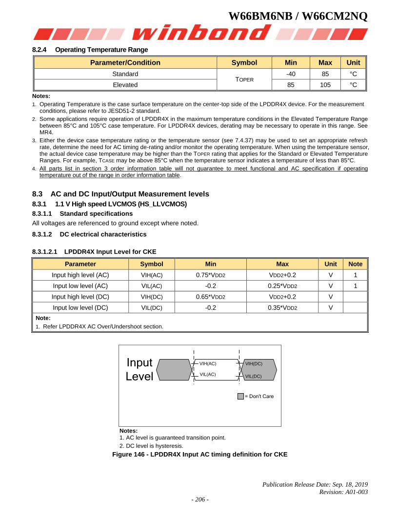
W66BM6NB / W66CM2NQ
Publication Release Date: Sep. 18, 2019
Revision: A01-003
- 206 -
8.2.4 Operating Temperature Range
Parameter/Condition Symbol Min Max Unit
Standard TOPER
-40 85 °C
Elevated 85 105 °C
Notes:
1. Operating Temperature is the case surface temperature on the center-top side of the LPDDR4X device. For the measurement conditions, please refer to JESD51-2 standard.
2. Some applications require operation of LPDDR4X in the maximum temperature conditions in the Elevated Temperature Range between 85°C and 105°C case temperature. For LPDDR4X devices, derating may be necessary to operate in this range. See MR4.
3. Either the device case temperature rating or the temperature sensor (see 7.4.37) may be used to set an appropriate refresh rate, determine the need for AC timing de-rating and/or monitor the operating temperature. When using the temperature sensor, the actual device case temperature may be higher than the TOPER rating that applies for the Standard or Elevated Temperature Ranges. For example, TCASE may be above 85°C when the temperature sensor indicates a temperature of less than 85°C.
4. All parts list in section 3 order information table will not guarantee to meet functional and AC specification if operating temperature out of the range in order information table.
8.3 AC and DC Input/Output Measurement levels
8.3.1 1.1 V High speed LVCMOS (HS_LLVCMOS)
8.3.1.1 Standard specifications
All voltages are referenced to ground except where noted.
8.3.1.2 DC electrical characteristics
8.3.1.2.1 LPDDR4X Input Level for CKE
Parameter Symbol Min Max Unit Note
Input high level (AC) VIH(AC) 0.75*VDD2 VDD2+0.2 V 1
Input low level (AC) VIL(AC) -0.2 0.25*VDD2 V 1
Input high level (DC) VIH(DC) 0.65*VDD2 VDD2+0.2 V
Input low level (DC) VIL(DC) -0.2 0.35*VDD2 V
Note:
1. Refer LPDDR4X AC Over/Undershoot section.
VIH(AC)
VIL(AC)
VIH(DC)
VIL(DC)
Input
Level
= Don't Care
Notes:
1. AC level is guaranteed transition point.
2. DC level is hysteresis.
Figure 146 - LPDDR4X Input AC timing definition for CKE
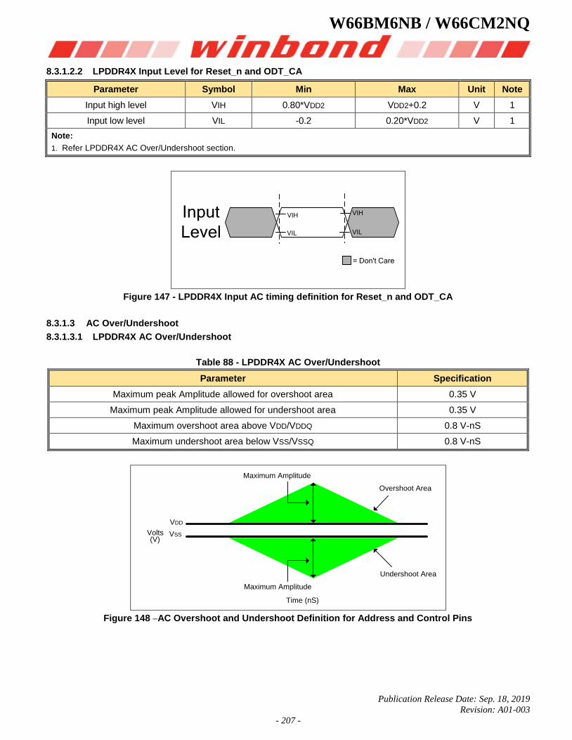
W66BM6NB / W66CM2NQ
Publication Release Date: Sep. 18, 2019
Revision: A01-003
- 207 -
8.3.1.2.2 LPDDR4X Input Level for Reset_n and ODT_CA
Parameter Symbol Min Max Unit Note
Input high level VIH 0.80*VDD2 VDD2+0.2 V 1
Input low level VIL -0.2 0.20*VDD2 V 1
Note:
1. Refer LPDDR4X AC Over/Undershoot section.
VIH
VIL
VIH
VIL
Input
Level
= Don't Care
Figure 147 - LPDDR4X Input AC timing definition for Reset_n and ODT_CA
8.3.1.3 AC Over/Undershoot
8.3.1.3.1 LPDDR4X AC Over/Undershoot
Table 88 - LPDDR4X AC Over/Undershoot
Parameter Specification
Maximum peak Amplitude allowed for overshoot area 0.35 V
Maximum peak Amplitude allowed for undershoot area 0.35 V
Maximum overshoot area above VDD/VDDQ 0.8 V-nS
Maximum undershoot area below VSS/VSSQ 0.8 V-nS
Maximum Amplitude
Maximum Amplitude
Overshoot Area
Undershoot Area
VDD
Volts
Time (nS)
VSS
(V)
Figure 148 –AC Overshoot and Undershoot Definition for Address and Control Pins
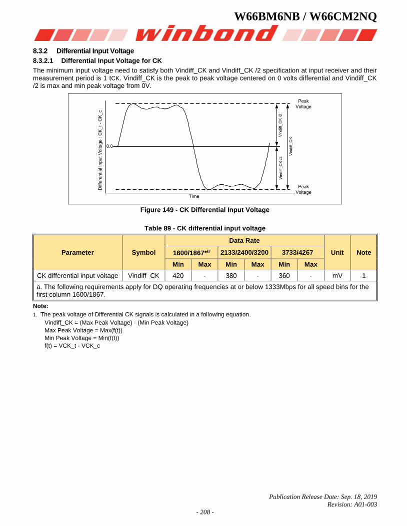
W66BM6NB / W66CM2NQ
Publication Release Date: Sep. 18, 2019
Revision: A01-003
- 208 -
8.3.2 Differential Input Voltage
8.3.2.1 Differential Input Voltage for CK
The minimum input voltage need to satisfy both Vindiff_CK and Vindiff_CK /2 specification at input receiver and their measurement period is 1 tCK. Vindiff_CK is the peak to peak voltage centered on 0 volts differential and Vindiff_CK /2 is max and min peak voltage from 0V.
Peak
Voltage
Peak
VoltageTime
0.0
Vin
diff_
CK
Vin
diff_
CK
/2
Vin
diff_
CK
/2
Diffe
ren
tia
l In
pu
t V
olta
ge
: C
K_
t -
CK
_c
Figure 149 - CK Differential Input Voltage
Table 89 - CK differential input voltage
Parameter Symbol
Data Rate
Unit Note 1600/1867*a 2133/2400/3200 3733/4267
Min Max Min Max Min Max
CK differential input voltage Vindiff_CK 420 - 380 - 360 - mV 1
a. The following requirements apply for DQ operating frequencies at or below 1333Mbps for all speed bins for the first column 1600/1867.
Note:
1. The peak voltage of Differential CK signals is calculated in a following equation.
Vindiff_CK = (Max Peak Voltage) - (Min Peak Voltage)
Max Peak Voltage = Max(f(t))
Min Peak Voltage = Min(f(t))
f(t) = VCK_t - VCK_c

W66BM6NB / W66CM2NQ
Publication Release Date: Sep. 18, 2019
Revision: A01-003
- 209 -
8.3.2.2 Peak voltage calculation method
The peak voltage of Differential Clock signals are calculated in a following equation.
VIH.DIFF.Peak Voltage = Max(f(t))
VIL.DIFF.Peak Voltage = Min(f(t))
f(t) = VCK_t - VCK_c
Time
Sin
gle
En
de
d I
np
ut
Vo
lta
ge
CK_t
CK_c
VREFCA
Min(f(t)) Max(f(t))
Note: 1. VREFCA is LPDDR4X SDRAM internal setting value by VREF Training.
Figure 150 - Definition of Differential Clock Peak Voltage
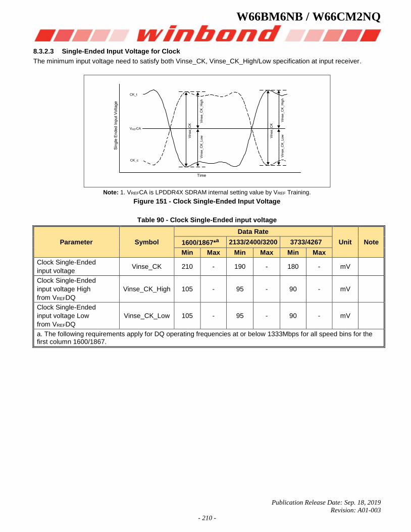
W66BM6NB / W66CM2NQ
Publication Release Date: Sep. 18, 2019
Revision: A01-003
- 210 -
8.3.2.3 Single-Ended Input Voltage for Clock
The minimum input voltage need to satisfy both Vinse_CK, Vinse_CK_High/Low specification at input receiver.
Time
Sin
gle
En
de
d I
np
ut
Vo
lta
ge
CK_t
CK_c
VREFCA
Vin
se
_C
K_
Hig
hV
inse
_C
K_
Lo
w
Vin
se
_C
K_
Hig
hV
inse
_C
K_
Lo
wVin
se
_C
K
Vin
se
_C
K
Note: 1. VREFCA is LPDDR4X SDRAM internal setting value by VREF Training.
Figure 151 - Clock Single-Ended Input Voltage
Table 90 - Clock Single-Ended input voltage
Parameter Symbol
Data Rate
Unit Note 1600/1867*a 2133/2400/3200 3733/4267
Min Max Min Max Min Max
Clock Single-Ended
input voltage Vinse_CK 210 - 190 - 180 - mV
Clock Single-Ended
input voltage High
from VREFDQ
Vinse_CK_High 105 - 95 - 90 - mV
Clock Single-Ended
input voltage Low
from VREFDQ
Vinse_CK_Low 105 - 95 - 90 - mV
a. The following requirements apply for DQ operating frequencies at or below 1333Mbps for all speed bins for the first column 1600/1867.
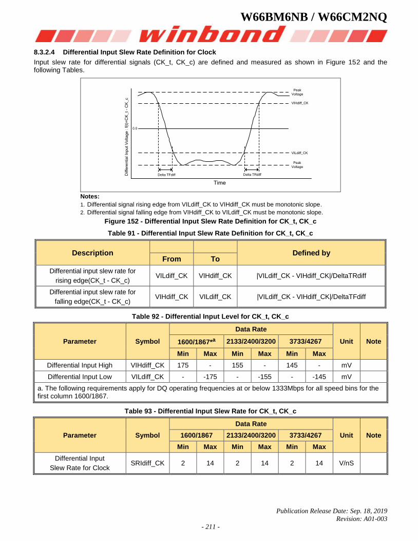
W66BM6NB / W66CM2NQ
Publication Release Date: Sep. 18, 2019
Revision: A01-003
- 211 -
8.3.2.4 Differential Input Slew Rate Definition for Clock
Input slew rate for differential signals (CK_t, CK_c) are defined and measured as shown in Figure 152 and the following Tables.
Delta TRdiffDelta TFdiff
Time
Peak
Voltage
Peak
Voltage
VIHdiff_CK
VILdiff_CK
0.0D
iffe
ren
tia
l In
pu
t V
olta
ge
: f
(t)=
CK
_t
- C
K_
c
Notes:
1. Differential signal rising edge from VILdiff_CK to VIHdiff_CK must be monotonic slope.
2. Differential signal falling edge from VIHdiff_CK to VILdiff_CK must be monotonic slope.
Figure 152 - Differential Input Slew Rate Definition for CK_t, CK_c
Table 91 - Differential Input Slew Rate Definition for CK_t, CK_c
Description
Defined by From To
Differential input slew rate for
rising edge(CK_t - CK_c) VILdiff_CK VIHdiff_CK |VILdiff_CK - VIHdiff_CK|/DeltaTRdiff
Differential input slew rate for
falling edge(CK_t - CK_c) VIHdiff_CK VILdiff_CK |VILdiff_CK - VIHdiff_CK|/DeltaTFdiff
Table 92 - Differential Input Level for CK_t, CK_c
Parameter Symbol
Data Rate
Unit Note 1600/1867*a 2133/2400/3200 3733/4267
Min Max Min Max Min Max
Differential Input High VIHdiff_CK 175 - 155 - 145 - mV
Differential Input Low VILdiff_CK - -175 - -155 - -145 mV
a. The following requirements apply for DQ operating frequencies at or below 1333Mbps for all speed bins for the first column 1600/1867.
Table 93 - Differential Input Slew Rate for CK_t, CK_c
Parameter Symbol
Data Rate
Unit Note 1600/1867 2133/2400/3200 3733/4267
Min Max Min Max Min Max
Differential Input
Slew Rate for Clock SRIdiff_CK 2 14 2 14 2 14 V/nS
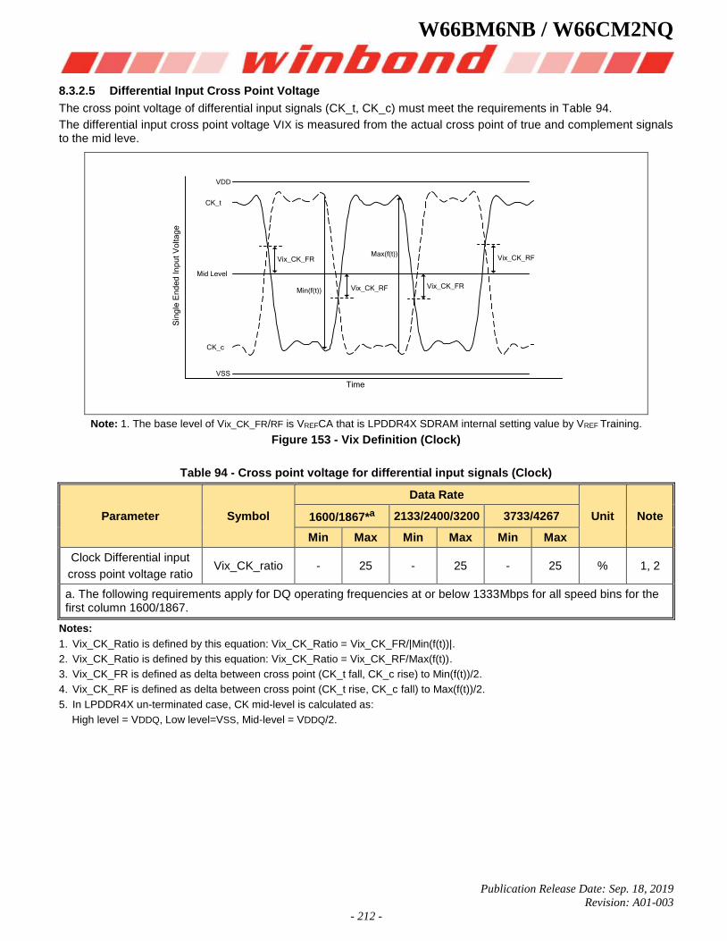
W66BM6NB / W66CM2NQ
Publication Release Date: Sep. 18, 2019
Revision: A01-003
- 212 -
8.3.2.5 Differential Input Cross Point Voltage
The cross point voltage of differential input signals (CK_t, CK_c) must meet the requirements in Table 94.
The differential input cross point voltage VIX is measured from the actual cross point of true and complement signals to the mid leve.
Time
Sin
gle
En
de
d I
np
ut
Vo
lta
ge
VDD
VSS
Vix_CK_RF
CK_t
CK_c
Mid Level
Vix_CK_FR
Min(f(t))
Max(f(t))
Vix_CK_RF Vix_CK_FR
Note: 1. The base level of Vix_CK_FR/RF is VREFCA that is LPDDR4X SDRAM internal setting value by VREF Training.
Figure 153 - Vix Definition (Clock)
Table 94 - Cross point voltage for differential input signals (Clock)
Parameter Symbol
Data Rate
Unit Note 1600/1867*a 2133/2400/3200 3733/4267
Min Max Min Max Min Max
Clock Differential input
cross point voltage ratio Vix_CK_ratio - 25 - 25 - 25 % 1, 2
a. The following requirements apply for DQ operating frequencies at or below 1333Mbps for all speed bins for the first column 1600/1867.
Notes:
1. Vix_CK_Ratio is defined by this equation: Vix_CK_Ratio = Vix_CK_FR/|Min(f(t))|.
2. Vix_CK_Ratio is defined by this equation: Vix_CK_Ratio = Vix_CK_RF/Max(f(t)).
3. Vix_CK_FR is defined as delta between cross point (CK_t fall, CK_c rise) to Min(f(t))/2.
4. Vix_CK_RF is defined as delta between cross point (CK_t rise, CK_c fall) to Max(f(t))/2.
5. In LPDDR4X un-terminated case, CK mid-level is calculated as:
High level = VDDQ, Low level=VSS, Mid-level = VDDQ/2.
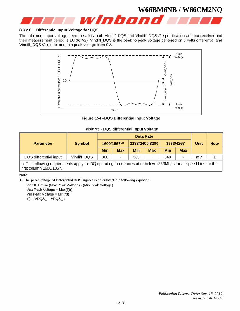
W66BM6NB / W66CM2NQ
Publication Release Date: Sep. 18, 2019
Revision: A01-003
- 213 -
8.3.2.6 Differential Input Voltage for DQS
The minimum input voltage need to satisfy both Vindiff_DQS and Vindiff_DQS /2 specification at input receiver and their measurement period is 1UI(tCK/2). Vindiff_DQS is the peak to peak voltage centered on 0 volts differential and Vindiff_DQS /2 is max and min peak voltage from 0V.
Peak
Voltage
Peak
VoltageTime
0.0
Vin
diff_
DQ
SVin
diff_
DQ
S /
2V
ind
iff_
DQ
S /
2
Diffe
ren
tia
l In
pu
t V
olta
ge
: D
QS
_t
- D
QS
_c
Figure 154 –DQS Differential Input Voltage
Table 95 - DQS differential input voltage
Parameter Symbol
Data Rate
Unit Note 1600/1867*a 2133/2400/3200 3733/4267
Min Max Min Max Min Max
DQS differential input Vindiff_DQS 360 - 360 - 340 - mV 1
a. The following requirements apply for DQ operating frequencies at or below 1333Mbps for all speed bins for the first column 1600/1867.
Note:
1. The peak voltage of Differential DQS signals is calculated in a following equation.
Vindiff_DQS= (Max Peak Voltage) - (Min Peak Voltage)
Max Peak Voltage = Max(f(t))
Min Peak Voltage = Min(f(t))
f(t) = VDQS_t - VDQS_c
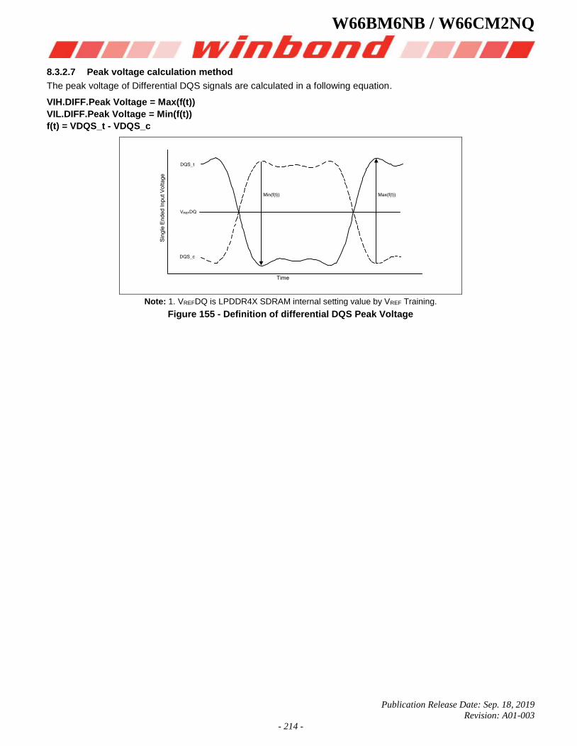
W66BM6NB / W66CM2NQ
Publication Release Date: Sep. 18, 2019
Revision: A01-003
- 214 -
8.3.2.7 Peak voltage calculation method
The peak voltage of Differential DQS signals are calculated in a following equation.
VIH.DIFF.Peak Voltage = Max(f(t))
VIL.DIFF.Peak Voltage = Min(f(t))
f(t) = VDQS_t - VDQS_c
Time
Sin
gle
En
de
d I
np
ut
Vo
lta
ge
DQS_t
DQS_c
VREFDQ
Min(f(t)) Max(f(t))
Note: 1. VREFDQ is LPDDR4X SDRAM internal setting value by VREF Training.
Figure 155 - Definition of differential DQS Peak Voltage
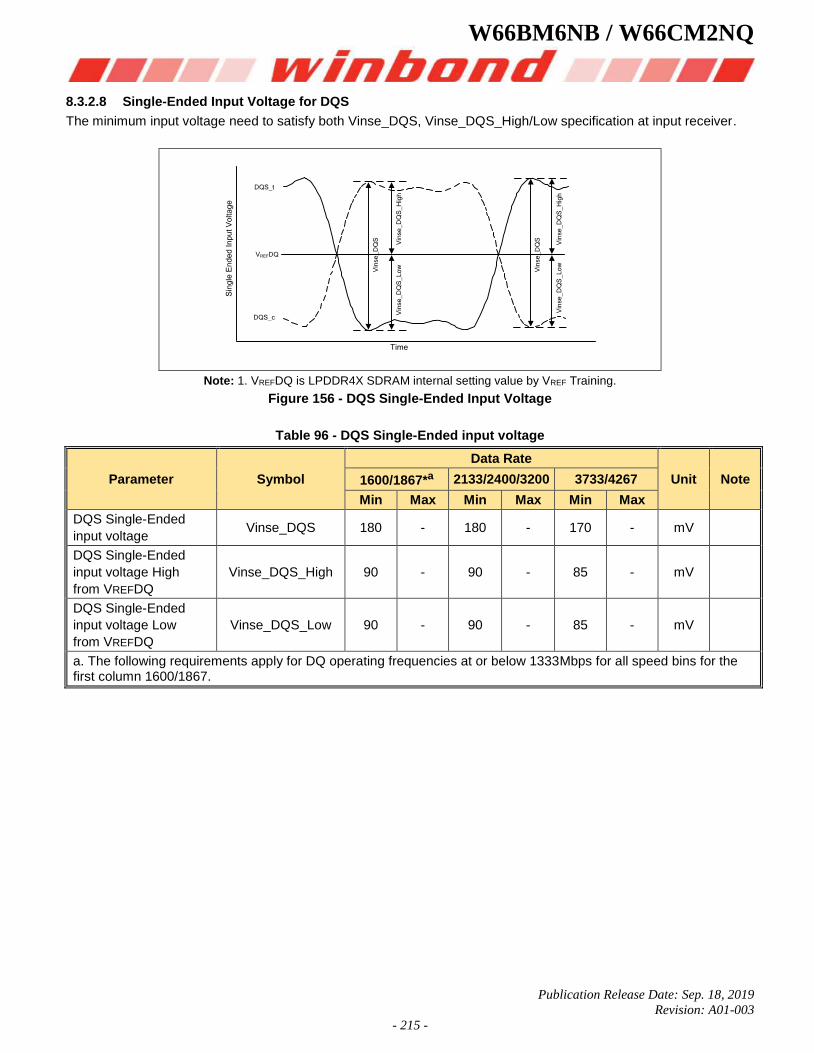
W66BM6NB / W66CM2NQ
Publication Release Date: Sep. 18, 2019
Revision: A01-003
- 215 -
8.3.2.8 Single-Ended Input Voltage for DQS
The minimum input voltage need to satisfy both Vinse_DQS, Vinse_DQS_High/Low specification at input receiver.
Time
Sin
gle
En
de
d I
np
ut
Vo
lta
ge
DQS_t
DQS_c
VREFDQ
Vin
se
_D
QS
_H
igh
Vin
se
_D
QS
_L
ow
Vin
se
_D
QS
_H
igh
Vin
se
_D
QS
_L
ow
Vin
se
_D
QS
Vin
se
_D
QS
Note: 1. VREFDQ is LPDDR4X SDRAM internal setting value by VREF Training.
Figure 156 - DQS Single-Ended Input Voltage
Table 96 - DQS Single-Ended input voltage
Parameter Symbol
Data Rate
Unit Note 1600/1867*a 2133/2400/3200 3733/4267
Min Max Min Max Min Max
DQS Single-Ended
input voltage Vinse_DQS 180 - 180 - 170 - mV
DQS Single-Ended
input voltage High
from VREFDQ
Vinse_DQS_High 90 - 90 - 85 - mV
DQS Single-Ended
input voltage Low
from VREFDQ
Vinse_DQS_Low 90 - 90 - 85 - mV
a. The following requirements apply for DQ operating frequencies at or below 1333Mbps for all speed bins for the first column 1600/1867.
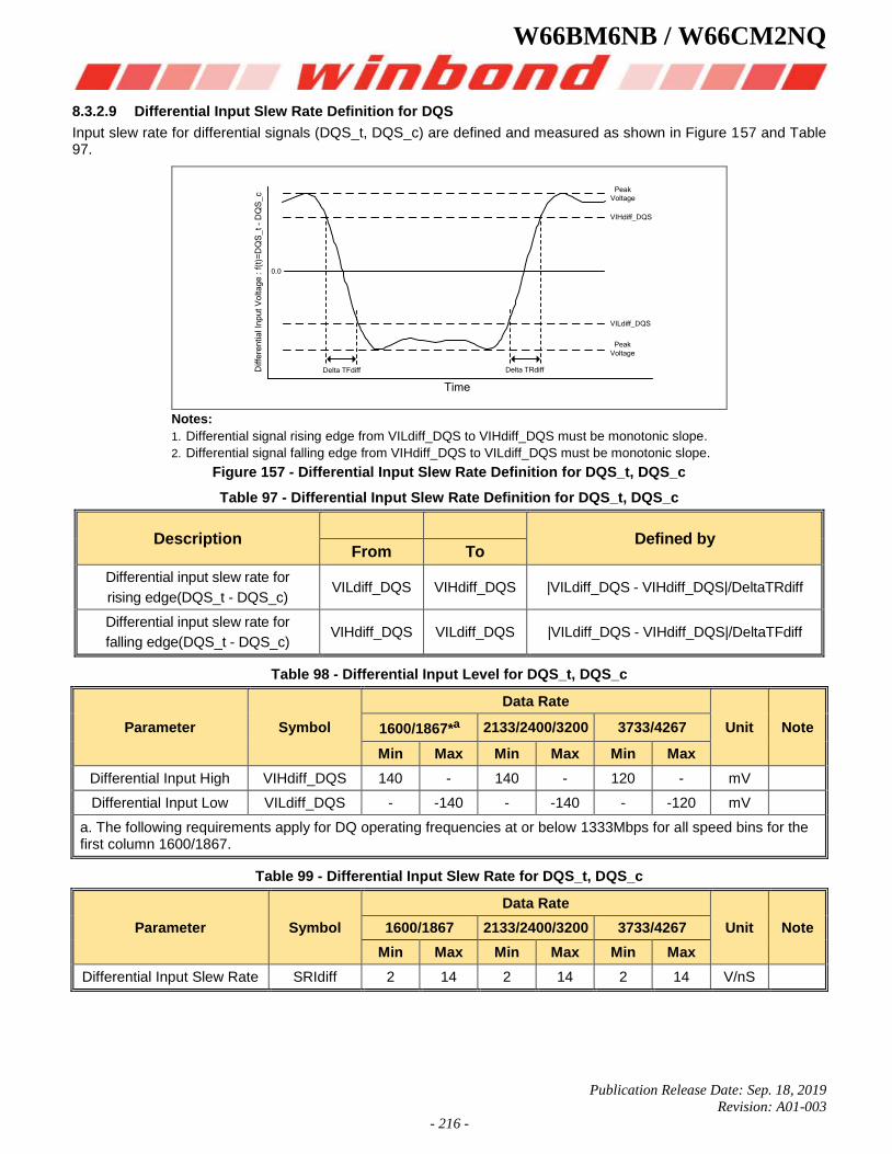
W66BM6NB / W66CM2NQ
Publication Release Date: Sep. 18, 2019
Revision: A01-003
- 216 -
8.3.2.9 Differential Input Slew Rate Definition for DQS
Input slew rate for differential signals (DQS_t, DQS_c) are defined and measured as shown in Figure 157 and Table 97.
Delta TRdiffDelta TFdiff
Time
Peak
Voltage
Peak
Voltage
VIHdiff_DQS
VILdiff_DQS
0.0
Diffe
ren
tia
l In
pu
t V
olta
ge
: f
(t)=
DQ
S_
t -
DQ
S_
c
Notes:
1. Differential signal rising edge from VILdiff_DQS to VIHdiff_DQS must be monotonic slope.
2. Differential signal falling edge from VIHdiff_DQS to VILdiff_DQS must be monotonic slope.
Figure 157 - Differential Input Slew Rate Definition for DQS_t, DQS_c
Table 97 - Differential Input Slew Rate Definition for DQS_t, DQS_c
Description
Defined by From To
Differential input slew rate for
rising edge(DQS_t - DQS_c) VILdiff_DQS VIHdiff_DQS |VILdiff_DQS - VIHdiff_DQS|/DeltaTRdiff
Differential input slew rate for
falling edge(DQS_t - DQS_c) VIHdiff_DQS VILdiff_DQS |VILdiff_DQS - VIHdiff_DQS|/DeltaTFdiff
Table 98 - Differential Input Level for DQS_t, DQS_c
Parameter Symbol
Data Rate
Unit Note 1600/1867*a 2133/2400/3200 3733/4267
Min Max Min Max Min Max
Differential Input High VIHdiff_DQS 140 - 140 - 120 - mV
Differential Input Low VILdiff_DQS - -140 - -140 - -120 mV
a. The following requirements apply for DQ operating frequencies at or below 1333Mbps for all speed bins for the first column 1600/1867.
Table 99 - Differential Input Slew Rate for DQS_t, DQS_c
Parameter Symbol
Data Rate
Unit Note 1600/1867 2133/2400/3200 3733/4267
Min Max Min Max Min Max
Differential Input Slew Rate SRIdiff 2 14 2 14 2 14 V/nS
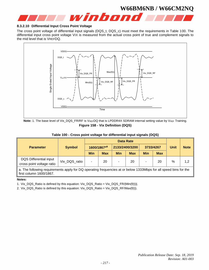
W66BM6NB / W66CM2NQ
Publication Release Date: Sep. 18, 2019
Revision: A01-003
- 217 -
8.3.2.10 Differential Input Cross Point Voltage
The cross point voltage of differential input signals (DQS_t, DQS_c) must meet the requirements in Table 100. The differential input cross point voltage VIX is measured from the actual cross point of true and complement signals to the mid level that is VREFDQ.
Time
Sin
gle
En
de
d I
np
ut
Vo
lta
ge
VDDQ
VSSQ
Vix_DQS_RF
DQS_t
DQS_c
VREFDQ
Vix_DQS_FR
Min(f(t))
Max(f(t))
Vix_DQS_RF Vix_DQS_FR
Note: 1. The base level of Vix_DQS_FR/RF is VREFDQ that is LPDDR4X SDRAM internal setting value by VREF Training.
Figure 158 - Vix Definition (DQS)
Table 100 - Cross point voltage for differential input signals (DQS)
Parameter Symbol
Data Rate
Unit Note 1600/1867*a 2133/2400/3200 3733/4267
Min Max Min Max Min Max
DQS Differential input
cross point voltage ratio Vix_DQS_ratio - 20 - 20 - 20 % 1,2
a. The following requirements apply for DQ operating frequencies at or below 1333Mbps for all speed bins for the first column 1600/1867.
Notes:
1. Vix_DQS_Ratio is defined by this equation: Vix_DQS_Ratio = Vix_DQS_FR/|Min(f(t))|.
2. Vix_DQS_Ratio is defined by this equation: Vix_DQS_Ratio = Vix_DQS_RF/Max(f(t)).
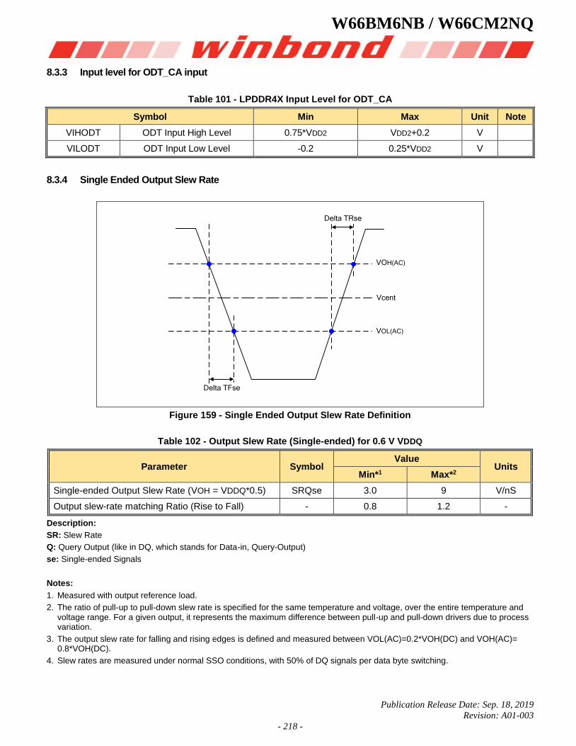
W66BM6NB / W66CM2NQ
Publication Release Date: Sep. 18, 2019
Revision: A01-003
- 218 -
8.3.3 Input level for ODT_CA input
Table 101 - LPDDR4X Input Level for ODT_CA
Symbol Min Max Unit Note
VIHODT ODT Input High Level 0.75*VDD2 VDD2+0.2 V
VILODT ODT Input Low Level -0.2 0.25*VDD2 V
8.3.4 Single Ended Output Slew Rate
VOH(AC)
Vcent
VOL(AC)
Delta TFse
Delta TRse
Figure 159 - Single Ended Output Slew Rate Definition
Table 102 - Output Slew Rate (Single-ended) for 0.6 V VDDQ
Parameter Symbol Value
Units Min*1 Max*2
Single-ended Output Slew Rate (VOH = VDDQ*0.5) SRQse 3.0 9 V/nS
Output slew-rate matching Ratio (Rise to Fall) - 0.8 1.2 -
Description:
SR: Slew Rate
Q: Query Output (like in DQ, which stands for Data-in, Query-Output)
se: Single-ended Signals
Notes:
1. Measured with output reference load.
2. The ratio of pull-up to pull-down slew rate is specified for the same temperature and voltage, over the entire temperature and voltage range. For a given output, it represents the maximum difference between pull-up and pull-down drivers due to process variation.
3. The output slew rate for falling and rising edges is defined and measured between VOL(AC)=0.2*VOH(DC) and VOH(AC)= 0.8*VOH(DC).
4. Slew rates are measured under normal SSO conditions, with 50% of DQ signals per data byte switching.
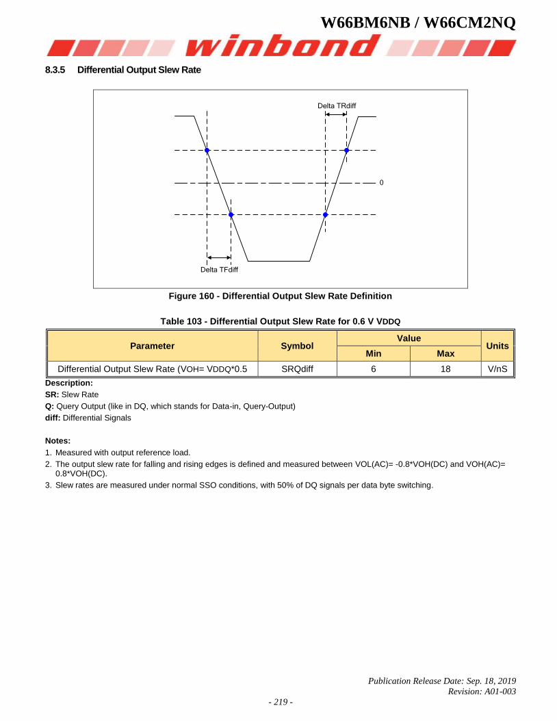
W66BM6NB / W66CM2NQ
Publication Release Date: Sep. 18, 2019
Revision: A01-003
- 219 -
8.3.5 Differential Output Slew Rate
0
Delta TFdiff
Delta TRdiff
Figure 160 - Differential Output Slew Rate Definition
Table 103 - Differential Output Slew Rate for 0.6 V VDDQ
Parameter Symbol Value
Units Min Max
Differential Output Slew Rate (VOH= VDDQ*0.5 SRQdiff 6 18 V/nS
Description:
SR: Slew Rate
Q: Query Output (like in DQ, which stands for Data-in, Query-Output)
diff: Differential Signals
Notes:
1. Measured with output reference load.
2. The output slew rate for falling and rising edges is defined and measured between VOL(AC)= -0.8*VOH(DC) and VOH(AC)= 0.8*VOH(DC).
3. Slew rates are measured under normal SSO conditions, with 50% of DQ signals per data byte switching.
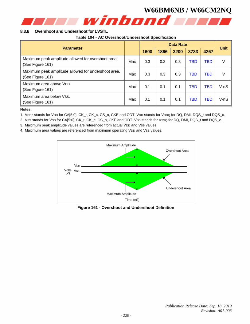
W66BM6NB / W66CM2NQ
Publication Release Date: Sep. 18, 2019
Revision: A01-003
- 220 -
8.3.6 Overshoot and Undershoot for LVSTL
Table 104 - AC Overshoot/Undershoot Specification
Parameter Data Rate
Unit 1600 1866 3200 3733 4267
Maximum peak amplitude allowed for overshoot area.
(See Figure 161) Max 0.3 0.3 0.3 TBD TBD V
Maximum peak amplitude allowed for undershoot area.
(See Figure 161) Max 0.3 0.3 0.3 TBD TBD V
Maximum area above VDD.
(See Figure 161) Max 0.1 0.1 0.1 TBD TBD V-nS
Maximum area below VSS.
(See Figure 161) Max 0.1 0.1 0.1 TBD TBD V-nS
Notes:
1. VDD2 stands for VDD for CA[5:0], CK_t, CK_c, CS_n, CKE and ODT. VDD stands for VDDQ for DQ, DMI, DQS_t and DQS_c.
2. VSS stands for VSS for CA[5:0], CK_t, CK_c, CS_n, CKE and ODT. VSS stands for VSSQ for DQ, DMI, DQS_t and DQS_c.
3. Maximum peak amplitude values are referenced from actual VDD and VSS values.
4. Maximum area values are referenced from maximum operating VDD and VSS values.
Maximum Amplitude
Maximum Amplitude
Overshoot Area
Undershoot Area
VDD
Volts
Time (nS)
VSS
(V)
Figure 161 - Overshoot and Undershoot Definition
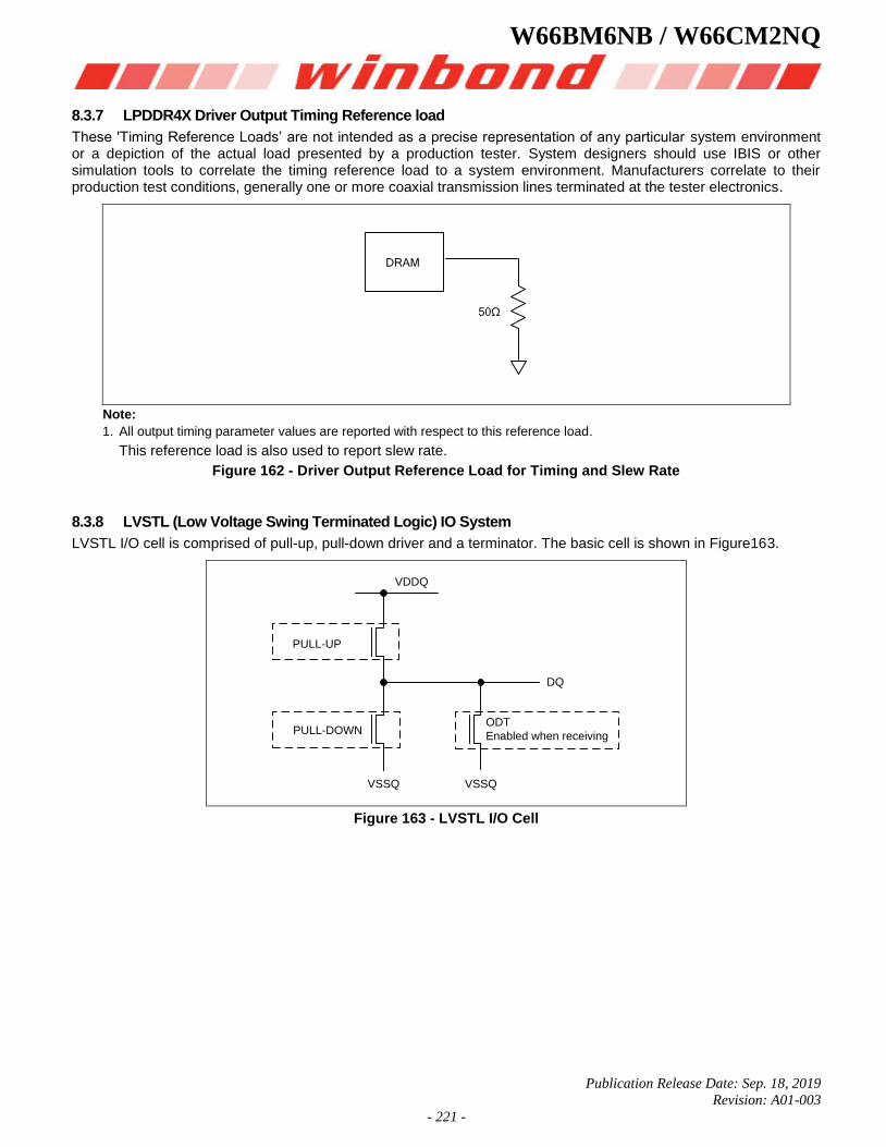
W66BM6NB / W66CM2NQ
Publication Release Date: Sep. 18, 2019
Revision: A01-003
- 221 -
8.3.7 LPDDR4X Driver Output Timing Reference load
These 'Timing Reference Loads’ are not intended as a precise representation of any particular system environment or a depiction of the actual load presented by a production tester. System designers should use IBIS or other simulation tools to correlate the timing reference load to a system environment. Manufacturers correlate to their production test conditions, generally one or more coaxial transmission lines terminated at the tester electronics.
DRAM
50Ω
Note:
1. All output timing parameter values are reported with respect to this reference load.
This reference load is also used to report slew rate.
Figure 162 - Driver Output Reference Load for Timing and Slew Rate
8.3.8 LVSTL (Low Voltage Swing Terminated Logic) IO System
LVSTL I/O cell is comprised of pull-up, pull-down driver and a terminator. The basic cell is shown in Figure163.
VDDQ
PULL-UP
PULL-DOWN
VSSQ VSSQ
ODT
Enabled when receiving
DQ
Figure 163 - LVSTL I/O Cell
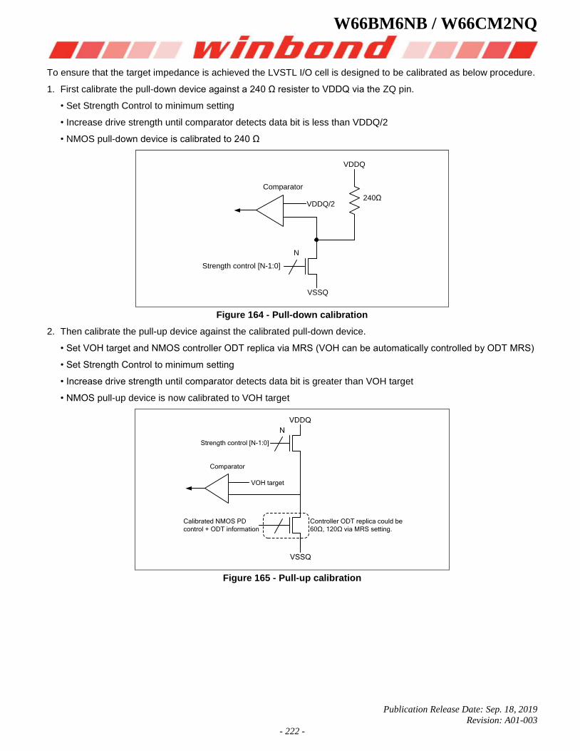
W66BM6NB / W66CM2NQ
Publication Release Date: Sep. 18, 2019
Revision: A01-003
- 222 -
To ensure that the target impedance is achieved the LVSTL I/O cell is designed to be calibrated as below procedure.
1. First calibrate the pull-down device against a 240 Ω resister to VDDQ via the ZQ pin.
• Set Strength Control to minimum setting
• Increase drive strength until comparator detects data bit is less than VDDQ/2
• NMOS pull-down device is calibrated to 240 Ω
VSSQ
VDDQ
VDDQ/2
Comparator
240Ω
N
Strength control [N-1:0]
Figure 164 - Pull-down calibration
2. Then calibrate the pull-up device against the calibrated pull-down device.
• Set VOH target and NMOS controller ODT replica via MRS (VOH can be automatically controlled by ODT MRS)
• Set Strength Control to minimum setting
• Increase drive strength until comparator detects data bit is greater than VOH target
• NMOS pull-up device is now calibrated to VOH target
VSSQ
N
Calibrated NMOS PD
control + ODT information
Controller ODT replica could be
60Ω, 120Ω via MRS setting.
Comparator
Strength control [N-1:0]
VOH target
VDDQ
Figure 165 - Pull-up calibration
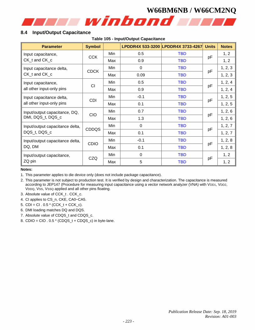
W66BM6NB / W66CM2NQ
Publication Release Date: Sep. 18, 2019
Revision: A01-003
- 223 -
8.4 Input/Output Capacitance
Table 105 - Input/Output Capacitance
Parameter Symbol LPDDR4X 533-3200 LPDDR4X 3733-4267 Units Notes
Input capacitance,
CK_t and CK_c CCK
Min 0.5 TBD pF
1, 2
Max 0.9 TBD 1, 2
Input capacitance delta,
CK_t and CK_c CDCK
Min 0 TBD pF
1, 2, 3
Max 0.09 TBD 1, 2, 3
Input capacitance,
all other input-only pins CI
Min 0.5 TBD pF
1, 2, 4
Max 0.9 TBD 1, 2, 4
Input capacitance delta,
all other input-only pins CDI
Min -0.1 TBD pF
1, 2, 5
Max 0.1 TBD 1, 2, 5
Input/output capacitance, DQ, DMI, DQS_t, DQS_c
CIO Min 0.7 TBD
pF 1, 2, 6
Max 1.3 TBD 1, 2, 6
Input/output capacitance delta,
DQS_t, DQS_c CDDQS
Min 0 TBD pF
1, 2, 7
Max 0.1 TBD 1, 2, 7
Input/output capacitance delta,
DQ, DM CDIO
Min -0.1 TBD pF
1, 2, 8
Max 0.1 TBD 1, 2, 8
Input/output capacitance,
ZQ pin CZQ
Min 0 TBD pF
1, 2
Max 5 TBD 1, 2
Notes:
1. This parameter applies to die device only (does not include package capacitance).
2. This parameter is not subject to production test. It is verified by design and characterization. The capacitance is measured according to JEP147 (Procedure for measuring input capacitance using a vector network analyzer (VNA) with VDD1, VDD2, VDDQ, VSS, VSSQ applied and all other pins floating.
3. Absolute value of CCK_t . CCK_c.
4. CI applies to CS_n, CKE, CA0~CA5.
5. CDI = CI . 0.5 * (CCK_t + CCK_c).
6. DMI loading matches DQ and DQS.
7. Absolute value of CDQS_t and CDQS_c.
8. CDIO = CIO . 0.5 * (CDQS_t + CDQS_c) in byte-lane.
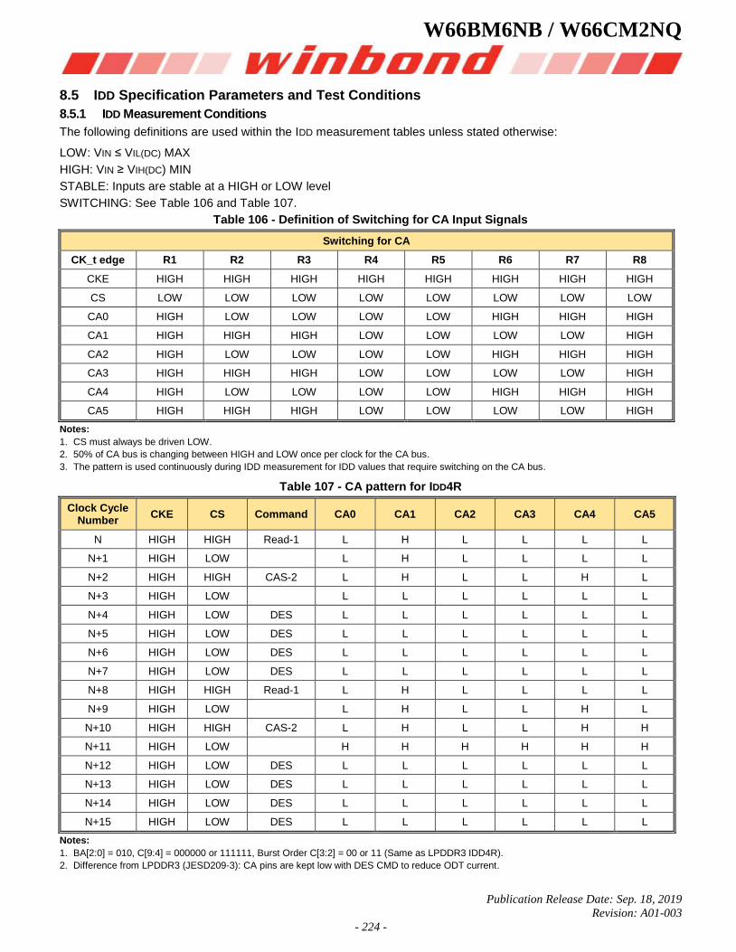
W66BM6NB / W66CM2NQ
Publication Release Date: Sep. 18, 2019
Revision: A01-003
- 224 -
8.5 IDD Specification Parameters and Test Conditions
8.5.1 IDD Measurement Conditions
The following definitions are used within the IDD measurement tables unless stated otherwise:
LOW: VIN ≤ VIL(DC) MAX
HIGH: VIN ≥ VIH(DC) MIN
STABLE: Inputs are stable at a HIGH or LOW level
SWITCHING: See Table 106 and Table 107.
Table 106 - Definition of Switching for CA Input Signals
Switching for CA
CK_t edge R1 R2 R3 R4 R5 R6 R7 R8
CKE HIGH HIGH HIGH HIGH HIGH HIGH HIGH HIGH
CS LOW LOW LOW LOW LOW LOW LOW LOW
CA0 HIGH LOW LOW LOW LOW HIGH HIGH HIGH
CA1 HIGH HIGH HIGH LOW LOW LOW LOW HIGH
CA2 HIGH LOW LOW LOW LOW HIGH HIGH HIGH
CA3 HIGH HIGH HIGH LOW LOW LOW LOW HIGH
CA4 HIGH LOW LOW LOW LOW HIGH HIGH HIGH
CA5 HIGH HIGH HIGH LOW LOW LOW LOW HIGH
Notes:
1. CS must always be driven LOW.
2. 50% of CA bus is changing between HIGH and LOW once per clock for the CA bus.
3. The pattern is used continuously during IDD measurement for IDD values that require switching on the CA bus.
Table 107 - CA pattern for IDD4R
Clock Cycle Number
CKE CS Command CA0 CA1 CA2 CA3 CA4 CA5
N HIGH HIGH Read-1 L H L L L L
N+1 HIGH LOW L H L L L L
N+2 HIGH HIGH CAS-2 L H L L H L
N+3 HIGH LOW L L L L L L
N+4 HIGH LOW DES L L L L L L
N+5 HIGH LOW DES L L L L L L
N+6 HIGH LOW DES L L L L L L
N+7 HIGH LOW DES L L L L L L
N+8 HIGH HIGH Read-1 L H L L L L
N+9 HIGH LOW L H L L H L
N+10 HIGH HIGH CAS-2 L H L L H H
N+11 HIGH LOW H H H H H H
N+12 HIGH LOW DES L L L L L L
N+13 HIGH LOW DES L L L L L L
N+14 HIGH LOW DES L L L L L L
N+15 HIGH LOW DES L L L L L L
Notes:
1. BA[2:0] = 010, C[9:4] = 000000 or 111111, Burst Order C[3:2] = 00 or 11 (Same as LPDDR3 IDD4R).
2. Difference from LPDDR3 (JESD209-3): CA pins are kept low with DES CMD to reduce ODT current.
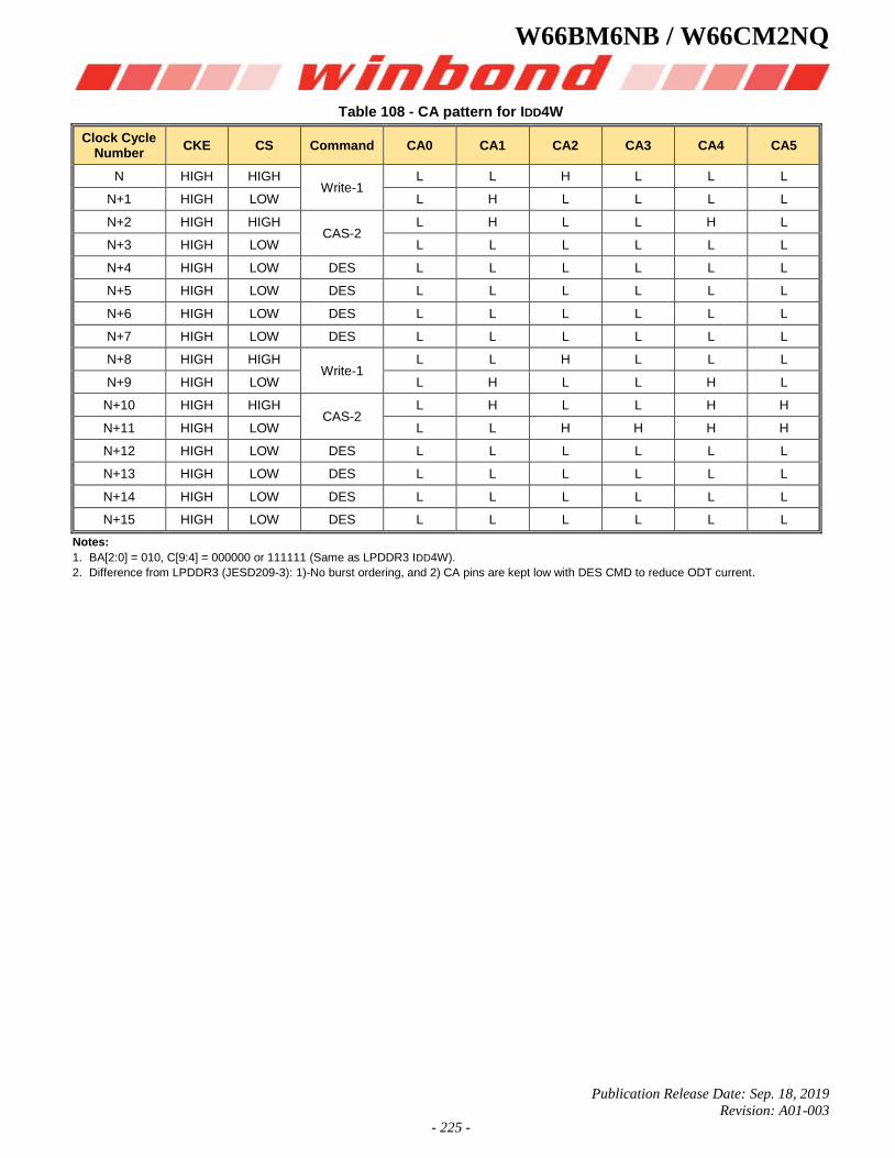
W66BM6NB / W66CM2NQ
Publication Release Date: Sep. 18, 2019
Revision: A01-003
- 225 -
Table 108 - CA pattern for IDD4W
Clock Cycle Number
CKE CS Command CA0 CA1 CA2 CA3 CA4 CA5
N HIGH HIGH Write-1
L L H L L L
N+1 HIGH LOW L H L L L L
N+2 HIGH HIGH CAS-2
L H L L H L
N+3 HIGH LOW L L L L L L
N+4 HIGH LOW DES L L L L L L
N+5 HIGH LOW DES L L L L L L
N+6 HIGH LOW DES L L L L L L
N+7 HIGH LOW DES L L L L L L
N+8 HIGH HIGH Write-1
L L H L L L
N+9 HIGH LOW L H L L H L
N+10 HIGH HIGH CAS-2
L H L L H H
N+11 HIGH LOW L L H H H H
N+12 HIGH LOW DES L L L L L L
N+13 HIGH LOW DES L L L L L L
N+14 HIGH LOW DES L L L L L L
N+15 HIGH LOW DES L L L L L L
Notes:
1. BA[2:0] = 010, C[9:4] = 000000 or 111111 (Same as LPDDR3 IDD4W).
2. Difference from LPDDR3 (JESD209-3): 1)-No burst ordering, and 2) CA pins are kept low with DES CMD to reduce ODT current.
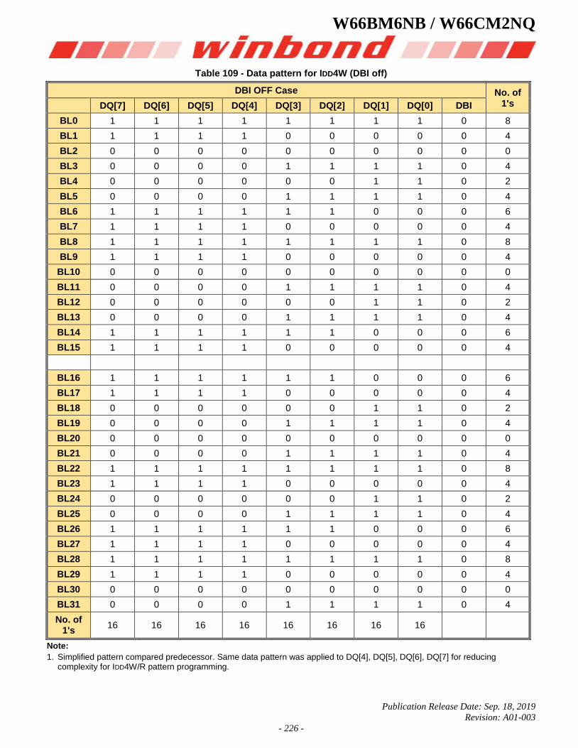
W66BM6NB / W66CM2NQ
Publication Release Date: Sep. 18, 2019
Revision: A01-003
- 226 -
Table 109 - Data pattern for IDD4W (DBI off)
DBI OFF Case No. of 1's DQ[7] DQ[6] DQ[5] DQ[4] DQ[3] DQ[2] DQ[1] DQ[0] DBI
BL0 1 1 1 1 1 1 1 1 0 8
BL1 1 1 1 1 0 0 0 0 0 4
BL2 0 0 0 0 0 0 0 0 0 0
BL3 0 0 0 0 1 1 1 1 0 4
BL4 0 0 0 0 0 0 1 1 0 2
BL5 0 0 0 0 1 1 1 1 0 4
BL6 1 1 1 1 1 1 0 0 0 6
BL7 1 1 1 1 0 0 0 0 0 4
BL8 1 1 1 1 1 1 1 1 0 8
BL9 1 1 1 1 0 0 0 0 0 4
BL10 0 0 0 0 0 0 0 0 0 0
BL11 0 0 0 0 1 1 1 1 0 4
BL12 0 0 0 0 0 0 1 1 0 2
BL13 0 0 0 0 1 1 1 1 0 4
BL14 1 1 1 1 1 1 0 0 0 6
BL15 1 1 1 1 0 0 0 0 0 4
BL16 1 1 1 1 1 1 0 0 0 6
BL17 1 1 1 1 0 0 0 0 0 4
BL18 0 0 0 0 0 0 1 1 0 2
BL19 0 0 0 0 1 1 1 1 0 4
BL20 0 0 0 0 0 0 0 0 0 0
BL21 0 0 0 0 1 1 1 1 0 4
BL22 1 1 1 1 1 1 1 1 0 8
BL23 1 1 1 1 0 0 0 0 0 4
BL24 0 0 0 0 0 0 1 1 0 2
BL25 0 0 0 0 1 1 1 1 0 4
BL26 1 1 1 1 1 1 0 0 0 6
BL27 1 1 1 1 0 0 0 0 0 4
BL28 1 1 1 1 1 1 1 1 0 8
BL29 1 1 1 1 0 0 0 0 0 4
BL30 0 0 0 0 0 0 0 0 0 0
BL31 0 0 0 0 1 1 1 1 0 4
No. of 1's
16 16 16 16 16 16 16 16
Note:
1. Simplified pattern compared predecessor. Same data pattern was applied to DQ[4], DQ[5], DQ[6], DQ[7] for reducing complexity for IDD4W/R pattern programming.
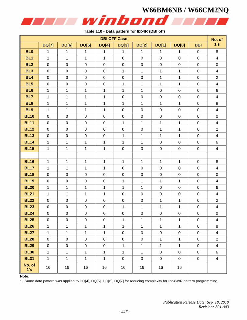
W66BM6NB / W66CM2NQ
Publication Release Date: Sep. 18, 2019
Revision: A01-003
- 227 -
Table 110 - Data pattern for IDD4R (DBI off)
DBI OFF Case No. of 1's DQ[7] DQ[6] DQ[5] DQ[4] DQ[3] DQ[2] DQ[1] DQ[0] DBI
BL0 1 1 1 1 1 1 1 1 0 8
BL1 1 1 1 1 0 0 0 0 0 4
BL2 0 0 0 0 0 0 0 0 0 0
BL3 0 0 0 0 1 1 1 1 0 4
BL4 0 0 0 0 0 0 1 1 0 2
BL5 0 0 0 0 1 1 1 1 0 4
BL6 1 1 1 1 1 1 0 0 0 6
BL7 1 1 1 1 0 0 0 0 0 4
BL8 1 1 1 1 1 1 1 1 0 8
BL9 1 1 1 1 0 0 0 0 0 4
BL10 0 0 0 0 0 0 0 0 0 0
BL11 0 0 0 0 1 1 1 1 0 4
BL12 0 0 0 0 0 0 1 1 0 2
BL13 0 0 0 0 1 1 1 1 0 4
BL14 1 1 1 1 1 1 0 0 0 6
BL15 1 1 1 1 0 0 0 0 0 4
BL16 1 1 1 1 1 1 1 1 0 8
BL17 1 1 1 1 0 0 0 0 0 4
BL18 0 0 0 0 0 0 0 0 0 0
BL19 0 0 0 0 1 1 1 1 0 4
BL20 1 1 1 1 1 1 0 0 0 6
BL21 1 1 1 1 0 0 0 0 0 4
BL22 0 0 0 0 0 0 1 1 0 2
BL23 0 0 0 0 1 1 1 1 0 4
BL24 0 0 0 0 0 0 0 0 0 0
BL25 0 0 0 0 1 1 1 1 0 4
BL26 1 1 1 1 1 1 1 1 0 8
BL27 1 1 1 1 0 0 0 0 0 4
BL28 0 0 0 0 0 0 1 1 0 2
BL29 0 0 0 0 1 1 1 1 0 4
BL30 1 1 1 1 1 1 0 0 0 6
BL31 1 1 1 1 0 0 0 0 0 4
No. of 1's
16 16 16 16 16 16 16 16
Note:
1. Same data pattern was applied to DQ[4], DQ[5], DQ[6], DQ[7] for reducing complexity for IDD4W/R pattern programming.
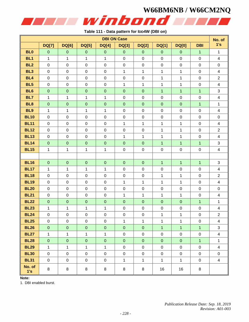
W66BM6NB / W66CM2NQ
Publication Release Date: Sep. 18, 2019
Revision: A01-003
- 228 -
Table 111 - Data pattern for IDD4W (DBI on)
DBI ON Case No. of 1's DQ[7] DQ[6] DQ[5] DQ[4] DQ[3] DQ[2] DQ[1] DQ[0] DBI
BL0 0 0 0 0 0 0 0 0 1 1
BL1 1 1 1 1 0 0 0 0 0 4
BL2 0 0 0 0 0 0 0 0 0 0
BL3 0 0 0 0 1 1 1 1 0 4
BL4 0 0 0 0 0 0 1 1 0 2
BL5 0 0 0 0 1 1 1 1 0 4
BL6 0 0 0 0 0 0 1 1 1 3
BL7 1 1 1 1 0 0 0 0 0 4
BL8 0 0 0 0 0 0 0 0 1 1
BL9 1 1 1 1 0 0 0 0 0 4
BL10 0 0 0 0 0 0 0 0 0 0
BL11 0 0 0 0 1 1 1 1 0 4
BL12 0 0 0 0 0 0 1 1 0 2
BL13 0 0 0 0 1 1 1 1 0 4
BL14 0 0 0 0 0 0 1 1 1 3
BL15 1 1 1 1 0 0 0 0 0 4
BL16 0 0 0 0 0 0 1 1 1 3
BL17 1 1 1 1 0 0 0 0 0 4
BL18 0 0 0 0 0 0 1 1 0 2
BL19 0 0 0 0 1 1 1 1 0 4
BL20 0 0 0 0 0 0 0 0 0 0
BL21 0 0 0 0 1 1 1 1 0 4
BL22 0 0 0 0 0 0 0 0 1 1
BL23 1 1 1 1 0 0 0 0 0 4
BL24 0 0 0 0 0 0 1 1 0 2
BL25 0 0 0 0 1 1 1 1 0 4
BL26 0 0 0 0 0 0 1 1 1 3
BL27 1 1 1 1 0 0 0 0 0 4
BL28 0 0 0 0 0 0 0 0 1 1
BL29 1 1 1 1 0 0 0 0 0 4
BL30 0 0 0 0 0 0 0 0 0 0
BL31 0 0 0 0 1 1 1 1 0 4
No. of 1's
8 8 8 8 8 8 16 16 8
Note:
1. DBI enabled burst.
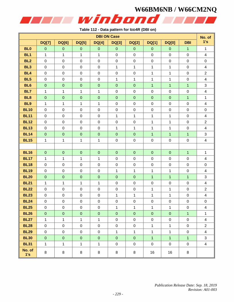
W66BM6NB / W66CM2NQ
Publication Release Date: Sep. 18, 2019
Revision: A01-003
- 229 -
Table 112 - Data pattern for IDD4R (DBI on)
DBI ON Case No. of 1's DQ[7] DQ[6] DQ[5] DQ[4] DQ[3] DQ[2] DQ[1] DQ[0] DBI
BL0 0 0 0 0 0 0 0 0 1 1
BL1 1 1 1 1 0 0 0 0 0 4
BL2 0 0 0 0 0 0 0 0 0 0
BL3 0 0 0 0 1 1 1 1 0 4
BL4 0 0 0 0 0 0 1 1 0 2
BL5 0 0 0 0 1 1 1 1 0 4
BL6 0 0 0 0 0 0 1 1 1 3
BL7 1 1 1 1 0 0 0 0 0 4
BL8 0 0 0 0 0 0 0 0 1 1
BL9 1 1 1 1 0 0 0 0 0 4
BL10 0 0 0 0 0 0 0 0 0 0
BL11 0 0 0 0 1 1 1 1 0 4
BL12 0 0 0 0 0 0 1 1 0 2
BL13 0 0 0 0 1 1 1 1 0 4
BL14 0 0 0 0 0 0 1 1 1 3
BL15 1 1 1 1 0 0 0 0 0 4
BL16 0 0 0 0 0 0 0 0 1 1
BL17 1 1 1 1 0 0 0 0 0 4
BL18 0 0 0 0 0 0 0 0 0 0
BL19 0 0 0 0 1 1 1 1 0 4
BL20 0 0 0 0 0 0 1 1 1 3
BL21 1 1 1 1 0 0 0 0 0 4
BL22 0 0 0 0 0 0 1 1 0 2
BL23 0 0 0 0 1 1 1 1 0 4
BL24 0 0 0 0 0 0 0 0 0 0
BL25 0 0 0 0 1 1 1 1 0 4
BL26 0 0 0 0 0 0 0 0 1 1
BL27 1 1 1 1 0 0 0 0 0 4
BL28 0 0 0 0 0 0 1 1 0 2
BL29 0 0 0 0 1 1 1 1 0 4
BL30 0 0 0 0 0 0 1 1 1 3
BL31 1 1 1 1 0 0 0 0 0 4
No. of 1's
8 8 8 8 8 8 16 16 8
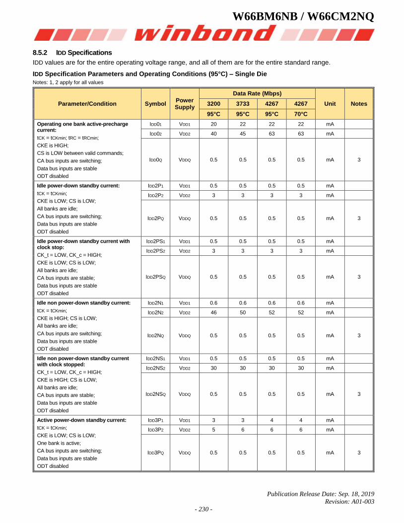
W66BM6NB / W66CM2NQ
Publication Release Date: Sep. 18, 2019
Revision: A01-003
- 230 -
8.5.2 IDD Specifications
IDD values are for the entire operating voltage range, and all of them are for the entire standard range.
IDD Specification Parameters and Operating Conditions (95°C) – Single Die
Notes: 1, 2 apply for all values
Parameter/Condition Symbol Power Supply
Data Rate (Mbps)
Unit Notes 3200 3733 4267 4267
95°C 95°C 95°C 70°C
Operating one bank active-precharge current:
tCK = tCKmin; tRC = tRCmin;
CKE is HIGH;
CS is LOW between valid commands;
CA bus inputs are switching;
Data bus inputs are stable
ODT disabled
IDD01 VDD1 20 22 22 22 mA
IDD02 VDD2 40 45 63 63 mA
IDD0Q VDDQ 0.5 0.5 0.5 0.5 mA 3
Idle power-down standby current:
tCK = tCKmin;
CKE is LOW; CS is LOW;
All banks are idle;
CA bus inputs are switching;
Data bus inputs are stable
ODT disabled
IDD2P1 VDD1 0.5 0.5 0.5 0.5 mA
IDD2P2 VDD2 3 3 3 3 mA
IDD2PQ VDDQ 0.5 0.5 0.5 0.5 mA 3
Idle power-down standby current with clock stop:
CK_t = LOW, CK_c = HIGH;
CKE is LOW; CS is LOW;
All banks are idle;
CA bus inputs are stable;
Data bus inputs are stable
ODT disabled
IDD2PS1 VDD1 0.5 0.5 0.5 0.5 mA
IDD2PS2 VDD2 3 3 3 3 mA
IDD2PSQ VDDQ 0.5 0.5 0.5 0.5 mA 3
Idle non power-down standby current:
tCK = tCKmin;
CKE is HIGH; CS is LOW;
All banks are idle;
CA bus inputs are switching;
Data bus inputs are stable
ODT disabled
IDD2N1 VDD1 0.6 0.6 0.6 0.6 mA
IDD2N2 VDD2 46 50 52 52 mA
IDD2NQ VDDQ 0.5 0.5 0.5 0.5 mA 3
Idle non power-down standby current with clock stopped:
CK_t = LOW, CK_c = HIGH;
CKE is HIGH; CS is LOW;
All banks are idle;
CA bus inputs are stable;
Data bus inputs are stable
ODT disabled
IDD2NS1 VDD1 0.5 0.5 0.5 0.5 mA
IDD2NS2 VDD2 30 30 30 30 mA
IDD2NSQ VDDQ 0.5 0.5 0.5 0.5 mA 3
Active power-down standby current:
tCK = tCKmin;
CKE is LOW; CS is LOW;
One bank is active;
CA bus inputs are switching;
Data bus inputs are stable
ODT disabled
IDD3P1 VDD1 3 3 4 4 mA
IDD3P2 VDD2 5 6 6 6 mA
IDD3PQ VDDQ 0.5 0.5 0.5 0.5 mA 3
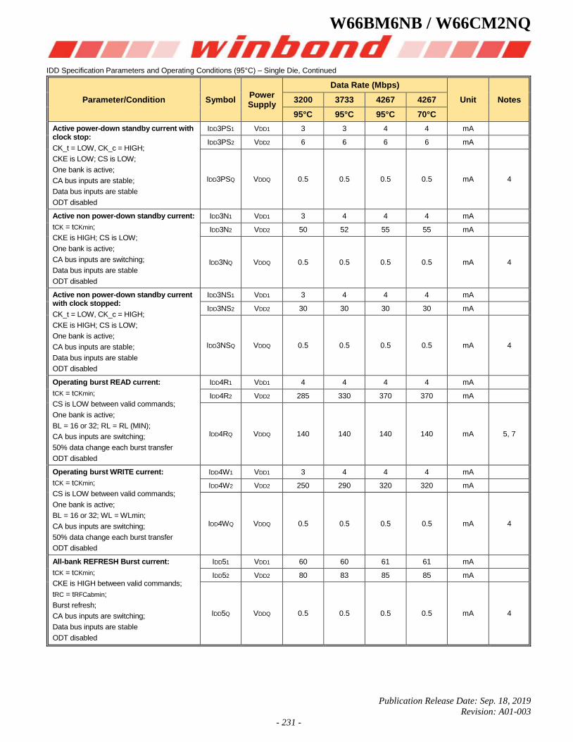
W66BM6NB / W66CM2NQ
Publication Release Date: Sep. 18, 2019
Revision: A01-003
- 231 -
IDD Specification Parameters and Operating Conditions (95°C) – Single Die, Continued
Parameter/Condition Symbol Power Supply
Data Rate (Mbps)
Unit Notes 3200 3733 4267 4267
95°C 95°C 95°C 70°C
Active power-down standby current with clock stop:
CK_t = LOW, CK_c = HIGH;
CKE is LOW; CS is LOW;
One bank is active;
CA bus inputs are stable;
Data bus inputs are stable
ODT disabled
IDD3PS1 VDD1 3 3 4 4 mA
IDD3PS2 VDD2 6 6 6 6 mA
IDD3PSQ VDDQ 0.5 0.5 0.5 0.5 mA 4
Active non power-down standby current:
tCK = tCKmin;
CKE is HIGH; CS is LOW;
One bank is active;
CA bus inputs are switching;
Data bus inputs are stable
ODT disabled
IDD3N1 VDD1 3 4 4 4 mA
IDD3N2 VDD2 50 52 55 55 mA
IDD3NQ VDDQ 0.5 0.5 0.5 0.5 mA 4
Active non power-down standby current with clock stopped:
CK_t = LOW, CK_c = HIGH;
CKE is HIGH; CS is LOW;
One bank is active;
CA bus inputs are stable;
Data bus inputs are stable
ODT disabled
IDD3NS1 VDD1 3 4 4 4 mA
IDD3NS2 VDD2 30 30 30 30 mA
IDD3NSQ VDDQ 0.5 0.5 0.5 0.5 mA 4
Operating burst READ current:
tCK = tCKmin;
CS is LOW between valid commands;
One bank is active;
BL = 16 or 32; RL = RL (MIN);
CA bus inputs are switching;
50% data change each burst transfer
ODT disabled
IDD4R1 VDD1 4 4 4 4 mA
IDD4R2 VDD2 285 330 370 370 mA
IDD4RQ VDDQ 140 140 140 140 mA 5, 7
Operating burst WRITE current:
tCK = tCKmin;
CS is LOW between valid commands;
One bank is active;
BL = 16 or 32; WL = WLmin;
CA bus inputs are switching;
50% data change each burst transfer
ODT disabled
IDD4W1 VDD1 3 4 4 4 mA
IDD4W2 VDD2 250 290 320 320 mA
IDD4WQ VDDQ 0.5 0.5 0.5 0.5 mA 4
All-bank REFRESH Burst current:
tCK = tCKmin;
CKE is HIGH between valid commands;
tRC = tRFCabmin;
Burst refresh;
CA bus inputs are switching;
Data bus inputs are stable
ODT disabled
IDD51 VDD1 60 60 61 61 mA
IDD52 VDD2 80 83 85 85 mA
IDD5Q VDDQ 0.5 0.5 0.5 0.5 mA 4
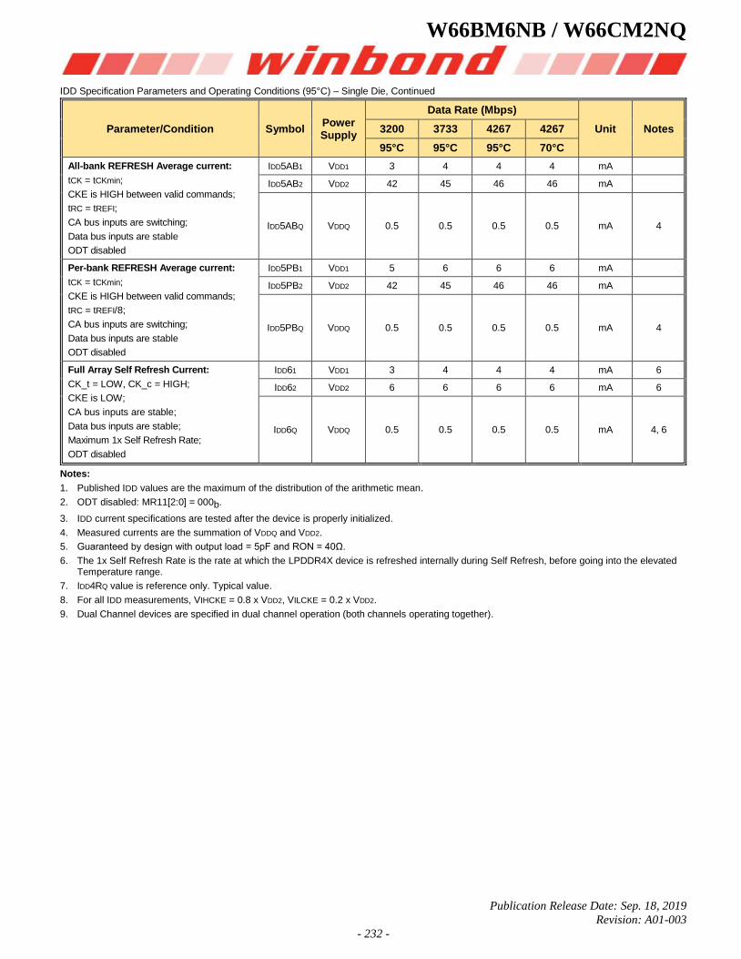
W66BM6NB / W66CM2NQ
Publication Release Date: Sep. 18, 2019
Revision: A01-003
- 232 -
IDD Specification Parameters and Operating Conditions (95°C) – Single Die, Continued
Parameter/Condition Symbol Power Supply
Data Rate (Mbps)
Unit Notes 3200 3733 4267 4267
95°C 95°C 95°C 70°C
All-bank REFRESH Average current:
tCK = tCKmin;
CKE is HIGH between valid commands;
tRC = tREFI;
CA bus inputs are switching;
Data bus inputs are stable
ODT disabled
IDD5AB1 VDD1 3 4 4 4 mA
IDD5AB2 VDD2 42 45 46 46 mA
IDD5ABQ VDDQ 0.5 0.5 0.5 0.5 mA 4
Per-bank REFRESH Average current:
tCK = tCKmin;
CKE is HIGH between valid commands;
tRC = tREFI/8;
CA bus inputs are switching;
Data bus inputs are stable
ODT disabled
IDD5PB1 VDD1 5 6 6 6 mA
IDD5PB2 VDD2 42 45 46 46 mA
IDD5PBQ VDDQ 0.5 0.5 0.5 0.5 mA 4
Full Array Self Refresh Current:
CK_t = LOW, CK_c = HIGH;
CKE is LOW;
CA bus inputs are stable;
Data bus inputs are stable;
Maximum 1x Self Refresh Rate;
ODT disabled
IDD61 VDD1 3 4 4 4 mA 6
IDD62 VDD2 6 6 6 6 mA 6
IDD6Q VDDQ 0.5 0.5 0.5 0.5 mA 4, 6
Notes:
1. Published IDD values are the maximum of the distribution of the arithmetic mean.
2. ODT disabled: MR11[2:0] = 000b.
3. IDD current specifications are tested after the device is properly initialized.
4. Measured currents are the summation of VDDQ and VDD2.
5. Guaranteed by design with output load = 5pF and RON = 40Ω.
6. The 1x Self Refresh Rate is the rate at which the LPDDR4X device is refreshed internally during Self Refresh, before going into the elevated Temperature range.
7. IDD4RQ value is reference only. Typical value.
8. For all IDD measurements, VIHCKE = 0.8 x VDD2, VILCKE = 0.2 x VDD2.
9. Dual Channel devices are specified in dual channel operation (both channels operating together).
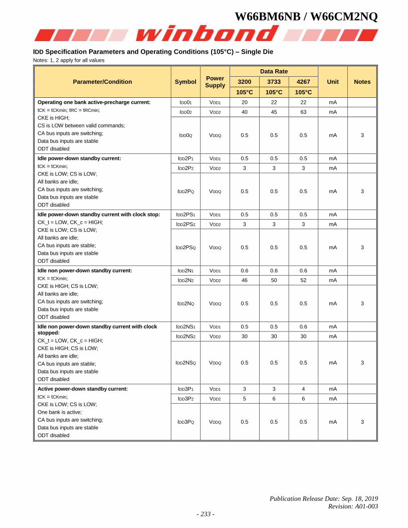
W66BM6NB / W66CM2NQ
Publication Release Date: Sep. 18, 2019
Revision: A01-003
- 233 -
IDD Specification Parameters and Operating Conditions (105°C) – Single Die
Notes: 1, 2 apply for all values
Parameter/Condition Symbol Power Supply
Data Rate
Unit Notes 3200 3733 4267
105°C 105°C 105°C
Operating one bank active-precharge current:
tCK = tCKmin; tRC = tRCmin;
CKE is HIGH;
CS is LOW between valid commands;
CA bus inputs are switching;
Data bus inputs are stable
ODT disabled
IDD01 VDD1 20 22 22 mA
IDD02 VDD2 40 45 63 mA
IDD0Q VDDQ 0.5 0.5 0.5 mA 3
Idle power-down standby current:
tCK = tCKmin;
CKE is LOW; CS is LOW;
All banks are idle;
CA bus inputs are switching;
Data bus inputs are stable
ODT disabled
IDD2P1 VDD1 0.5 0.5 0.5 mA
IDD2P2 VDD2 3 3 3 mA
IDD2PQ VDDQ 0.5 0.5 0.5 mA 3
Idle power-down standby current with clock stop:
CK_t = LOW, CK_c = HIGH;
CKE is LOW; CS is LOW;
All banks are idle;
CA bus inputs are stable;
Data bus inputs are stable
ODT disabled
IDD2PS1 VDD1 0.5 0.5 0.5 mA
IDD2PS2 VDD2 3 3 3 mA
IDD2PSQ VDDQ 0.5 0.5 0.5 mA 3
Idle non power-down standby current:
tCK = tCKmin;
CKE is HIGH; CS is LOW;
All banks are idle;
CA bus inputs are switching;
Data bus inputs are stable
ODT disabled
IDD2N1 VDD1 0.6 0.6 0.6 mA
IDD2N2 VDD2 46 50 52 mA
IDD2NQ VDDQ 0.5 0.5 0.5 mA 3
Idle non power-down standby current with clock stopped:
CK_t = LOW, CK_c = HIGH;
CKE is HIGH; CS is LOW;
All banks are idle;
CA bus inputs are stable;
Data bus inputs are stable
ODT disabled
IDD2NS1 VDD1 0.5 0.5 0.6 mA
IDD2NS2 VDD2 30 30 30 mA
IDD2NSQ VDDQ 0.5 0.5 0.5 mA 3
Active power-down standby current:
tCK = tCKmin;
CKE is LOW; CS is LOW;
One bank is active;
CA bus inputs are switching;
Data bus inputs are stable
ODT disabled
IDD3P1 VDD1 3 3 4 mA
IDD3P2 VDD2 5 6 6 mA
IDD3PQ VDDQ 0.5 0.5 0.5 mA 3
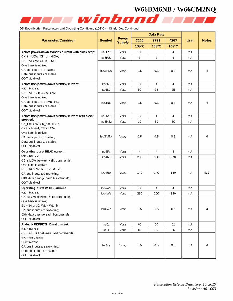
W66BM6NB / W66CM2NQ
Publication Release Date: Sep. 18, 2019
Revision: A01-003
- 234 -
IDD Specification Parameters and Operating Conditions (105°C) – Single Die, Continued
Parameter/Condition Symbol Power Supply
Data Rate
Unit Notes 3200 3733 4267
105°C 105°C 105°C
Active power-down standby current with clock stop:
CK_t = LOW, CK_c = HIGH;
CKE is LOW; CS is LOW;
One bank is active;
CA bus inputs are stable;
Data bus inputs are stable
ODT disabled
IDD3PS1 VDD1 3 3 4 mA
IDD3PS2 VDD2 6 6 6 mA
IDD3PSQ VDDQ 0.5 0.5 0.5 mA 4
Active non power-down standby current:
tCK = tCKmin;
CKE is HIGH; CS is LOW;
One bank is active;
CA bus inputs are switching;
Data bus inputs are stable
ODT disabled
IDD3N1 VDD1 3 4 4 mA
IDD3N2 VDD2 50 52 55 mA
IDD3NQ VDDQ 0.5 0.5 0.5 mA 4
Active non power-down standby current with clock stopped:
CK_t = LOW, CK_c = HIGH;
CKE is HIGH; CS is LOW;
One bank is active;
CA bus inputs are stable;
Data bus inputs are stable
ODT disabled
IDD3NS1 VDD1 3 4 4 mA
IDD3NS2 VDD2 30 30 30 mA
IDD3NSQ VDDQ 0.5 0.5 0.5 mA 4
Operating burst READ current:
tCK = tCKmin;
CS is LOW between valid commands;
One bank is active;
BL = 16 or 32; RL = RL (MIN);
CA bus inputs are switching;
50% data change each burst transfer
ODT disabled
IDD4R1 VDD1 4 4 4 mA
IDD4R2 VDD2 285 330 370 mA
IDD4RQ VDDQ 140 140 140 mA 5, 7
Operating burst WRITE current:
tCK = tCKmin;
CS is LOW between valid commands;
One bank is active;
BL = 16 or 32; WL = WLmin;
CA bus inputs are switching;
50% data change each burst transfer
ODT disabled
IDD4W1 VDD1 3 4 4 mA
IDD4W2 VDD2 250 290 320 mA
IDD4WQ VDDQ 0.5 0.5 0.5 mA 4
All-bank REFRESH Burst current:
tCK = tCKmin;
CKE is HIGH between valid commands;
tRC = tRFCabmin;
Burst refresh;
CA bus inputs are switching;
Data bus inputs are stable
ODT disabled
IDD51 VDD1 60 60 61 mA
IDD52 VDD2 80 83 85 mA
IDD5Q VDDQ 0.5 0.5 0.5 mA 4
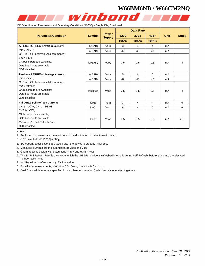
W66BM6NB / W66CM2NQ
Publication Release Date: Sep. 18, 2019
Revision: A01-003
- 235 -
IDD Specification Parameters and Operating Conditions (105°C) – Single Die, Continued
Parameter/Condition Symbol Power Supply
Data Rate
Unit Notes 3200 3733 4267
105°C 105°C 105°C
All-bank REFRESH Average current:
tCK = tCKmin;
CKE is HIGH between valid commands;
tRC = tREFI;
CA bus inputs are switching;
Data bus inputs are stable
ODT disabled
IDD5AB1 VDD1 3 4 4 mA
IDD5AB2 VDD2 42 45 46 mA
IDD5ABQ VDDQ 0.5 0.5 0.5 mA 4
Per-bank REFRESH Average current:
tCK = tCKmin;
CKE is HIGH between valid commands;
tRC = tREFI/8;
CA bus inputs are switching;
Data bus inputs are stable
ODT disabled
IDD5PB1 VDD1 5 6 6 mA
IDD5PB2 VDD2 42 45 46 mA
IDD5PBQ VDDQ 0.5 0.5 0.5 mA 4
Full Array Self Refresh Current:
CK_t = LOW, CK_c = HIGH;
CKE is LOW;
CA bus inputs are stable;
Data bus inputs are stable;
Maximum 1x Self Refresh Rate;
ODT disabled
IDD61 VDD1 3 4 4 mA 6
IDD62 VDD2 6 6 6 mA 6
IDD6Q VDDQ 0.5 0.5 0.5 mA 4, 6
Notes:
1. Published IDD values are the maximum of the distribution of the arithmetic mean.
2. ODT disabled: MR11[2:0] = 000b.
3. IDD current specifications are tested after the device is properly initialized.
4. Measured currents are the summation of VDDQ and VDD2.
5. Guaranteed by design with output load = 5pF and RON = 40Ω.
6. The 1x Self Refresh Rate is the rate at which the LPDDR4 device is refreshed internally during Self Refresh, before going into the elevated Temperature range.
7. IDD4RQ value is reference only. Typical value.
8. For all IDD measurements, VIHCKE = 0.8 x VDD2, VILCKE = 0.2 x VDD2.
9. Dual Channel devices are specified in dual channel operation (both channels operating together).
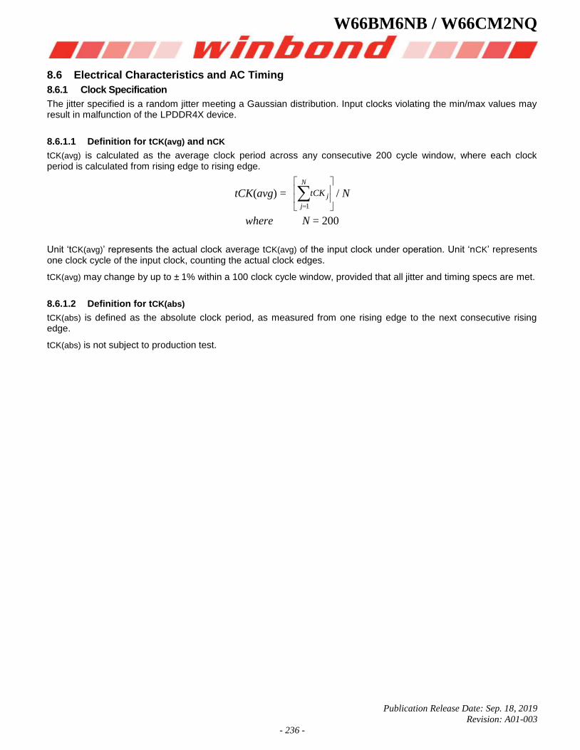
W66BM6NB / W66CM2NQ
Publication Release Date: Sep. 18, 2019
Revision: A01-003
- 236 -
8.6 Electrical Characteristics and AC Timing
8.6.1 Clock Specification
The jitter specified is a random jitter meeting a Gaussian distribution. Input clocks violating the min/max values may result in malfunction of the LPDDR4X device.
8.6.1.1 Definition for tCK(avg) and nCK
tCK(avg) is calculated as the average clock period across any consecutive 200 cycle window, where each clock period is calculated from rising edge to rising edge.
tCK(avg) =
N
j
jtCK
1
/ N
where N = 200
Unit ‘tCK(avg)’ represents the actual clock average tCK(avg) of the input clock under operation. Unit ‘nCK’ represents one clock cycle of the input clock, counting the actual clock edges.
tCK(avg) may change by up to ± 1% within a 100 clock cycle window, provided that all jitter and timing specs are met.
8.6.1.2 Definition for tCK(abs)
tCK(abs) is defined as the absolute clock period, as measured from one rising edge to the next consecutive rising edge.
tCK(abs) is not subject to production test.
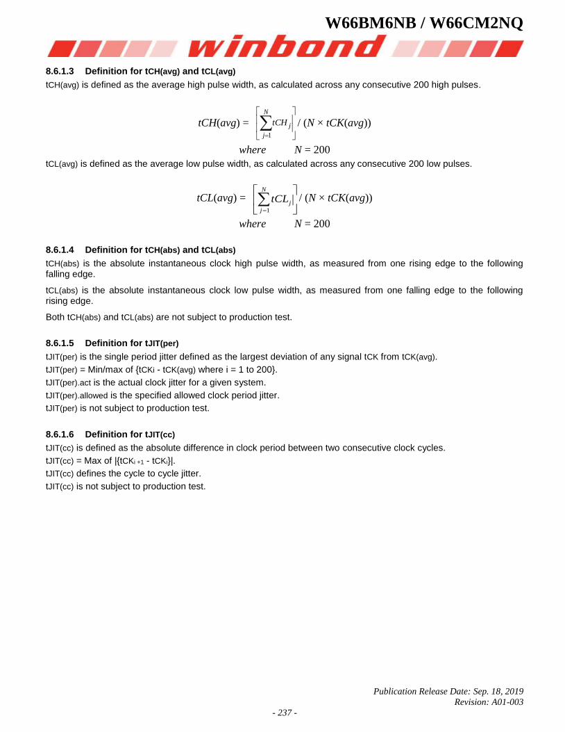
W66BM6NB / W66CM2NQ
Publication Release Date: Sep. 18, 2019
Revision: A01-003
- 237 -
8.6.1.3 Definition for tCH(avg) and tCL(avg)
tCH(avg) is defined as the average high pulse width, as calculated across any consecutive 200 high pulses.
tCH(avg) =
N
j
jtCH
1
/ (N × tCK(avg))
where N = 200
tCL(avg) is defined as the average low pulse width, as calculated across any consecutive 200 low pulses.
tCL(avg) =
N
j
jtCL1
/ (N × tCK(avg))
where N = 200
8.6.1.4 Definition for tCH(abs) and tCL(abs)
tCH(abs) is the absolute instantaneous clock high pulse width, as measured from one rising edge to the following falling edge.
tCL(abs) is the absolute instantaneous clock low pulse width, as measured from one falling edge to the following rising edge.
Both tCH(abs) and tCL(abs) are not subject to production test.
8.6.1.5 Definition for tJIT(per)
tJIT(per) is the single period jitter defined as the largest deviation of any signal tCK from tCK(avg).
tJIT(per) = Min/max of {tCKi - tCK(avg) where i = 1 to 200}.
tJIT(per).act is the actual clock jitter for a given system.
tJIT(per).allowed is the specified allowed clock period jitter.
tJIT(per) is not subject to production test.
8.6.1.6 Definition for tJIT(cc)
tJIT(cc) is defined as the absolute difference in clock period between two consecutive clock cycles.
tJIT(cc) = Max of |{tCKi +1 - tCKi}|.
tJIT(cc) defines the cycle to cycle jitter.
tJIT(cc) is not subject to production test.
W66BM6NB / W66CM2NQ
Publication Release Date: Sep. 18, 2019
Revision: A01-003
- 238 -
8.6.2 Clock AC Timing
Table 113 - Clock AC Timing
Parameter Symbol Min/Max
Data Rate Unit Note
1600 2400 3200 3733 4267
Average clock period tCK(avg) Min 1.25 0.833 0.625 0.535 0.468
nS Max 100 100 100 100 100
Average High pulse width tCH(avg) Min 0.46 0.46 0.46 TBD TBD
tCK(avg) Max 0.54 0.54 0.54 TBD TBD
Average Low pulse width tCL(avg) Min 0.46 0.46 0.46 TBD TBD
tCK(avg) Max 0.54 0.54 0.54 TBD TBD
Absolute clock period tCK(abs) Min tCK(avg)min + tJIT(per)min
nS Max -
Absolute High clock pulse width
tCH(abs) Min 0.43 0.43 0.43 TBD TBD
tCK(avg) Max 0.57 0.57 0.57 TBD TBD
Absolute Low clock pulse width
tCL(abs) Min 0.43 0.43 0.43 TBD TBD
tCK(avg) Max 0.57 0.57 0.57 TBD TBD
Clock period jitter tJIT(per) Min -70 -50 -40 - -
pS Max 70 50 40 TBD TBD
Maximum Clock Jitter between consecutive cycles
tJIT(cc) Min - - - - -
pS Max 140 100 80 TBD TBD
Note:
1. All parts list in section 3 order information table will not guarantee to meet functional and AC specification if the tCK(avg) out of range mentioned in above table.
8.6.3 Temperature Derating for AC timing
Table 114 - Temperature Derating AC Timing
Parameter Symbol Min/Max
Data Rate Unit
533 1066 1600 2133 2667 3200 3733 4267
Temperature Derating*1
DQS output access time
from CK_t/CK_c (derated) tDQSCK Max 3600 pS
RAS-to-CAS delay (derated) tRCD Min tRCD + 1.875 nS
ACTIVATE-to- ACTIVATE
command period (derated) tRC Min tRC + 3.75
nS
nS
Row active time (derated) tRAS Min tRAS + 1.875 nS
Row precharge time (derated) tRP Min tRP + 1.875 nS
Active bank A to
active bank B (derated) tRRD Min tRRD + 1.875 nS
Note:
1. At higher temperatures (>85°C), AC timing derating may be required. If derating is required the LPDDR4-SDRAM will set MR4 OP[2:0]=110b.
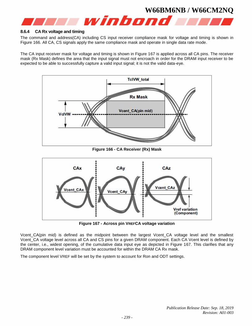
W66BM6NB / W66CM2NQ
Publication Release Date: Sep. 18, 2019
Revision: A01-003
- 239 -
8.6.4 CA Rx voltage and timing
The command and address(CA) including CS input receiver compliance mask for voltage and timing is shown in Figure 166. All CA, CS signals apply the same compliance mask and operate in single data rate mode.
The CA input receiver mask for voltage and timing is shown in Figure 167 is applied across all CA pins. The receiver mask (Rx Mask) defines the area that the input signal must not encroach in order for the DRAM input receiver to be expected to be able to successfully capture a valid input signal; it is not the valid data-eye.
Figure 166 - CA Receiver (Rx) Mask
Figure 167 - Across pin VREFCA voltage variation
Vcent_CA(pin mid) is defined as the midpoint between the largest Vcent_CA voltage level and the smallest Vcent_CA voltage level across all CA and CS pins for a given DRAM component. Each CA Vcent level is defined by the center, i.e., widest opening, of the cumulative data input eye as depicted in Figure 167. This clarifies that any DRAM component level variation must be accounted for within the DRAM CA Rx mask.
The component level VREF will be set by the system to account for Ron and ODT settings.
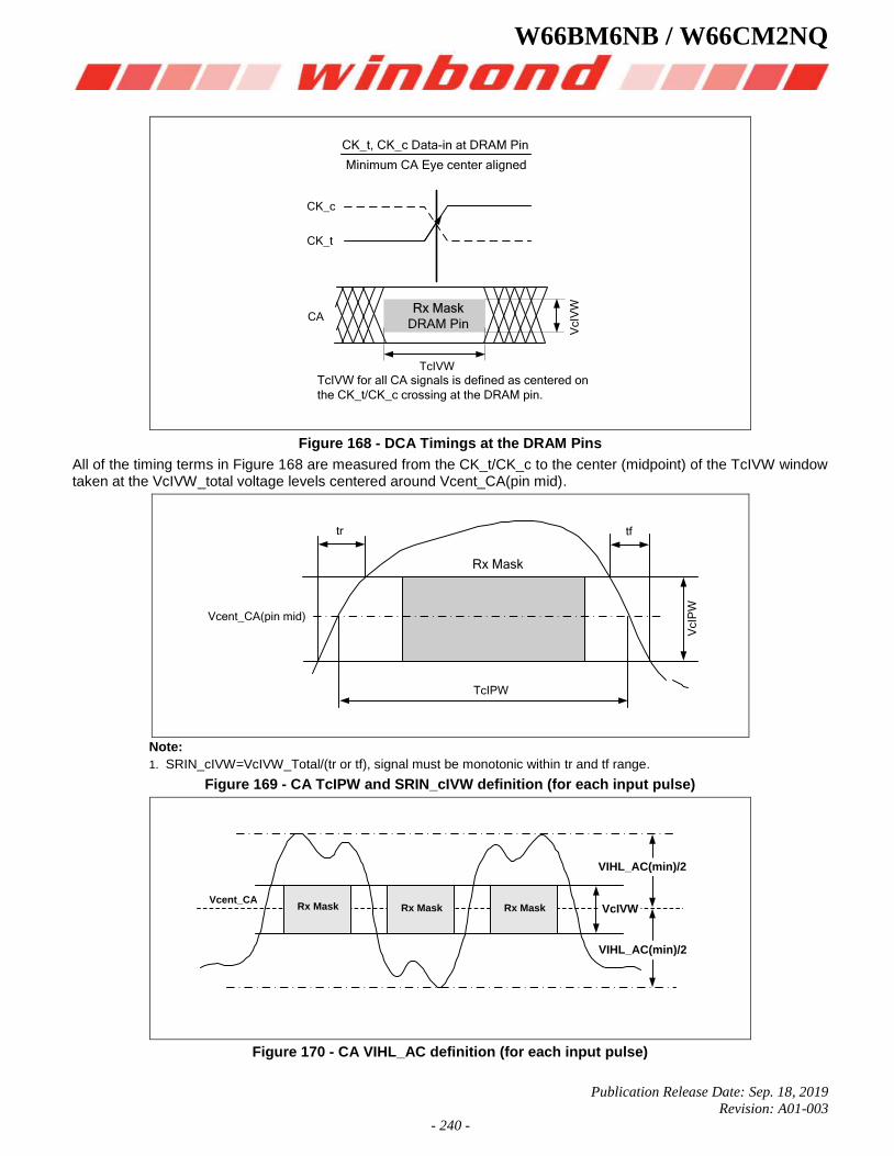
W66BM6NB / W66CM2NQ
Publication Release Date: Sep. 18, 2019
Revision: A01-003
- 240 -
CK_t, CK_c Data-in at DRAM Pin
Minimum CA Eye center aligned
Rx Mask
TcIVW
TcIVW for all CA signals is defined as centered on
the CK_t/CK_c crossing at the DRAM pin.
CK_c
CK_t
CADRAM Pin
VcIV
W
Figure 168 - DCA Timings at the DRAM Pins
All of the timing terms in Figure 168 are measured from the CK_t/CK_c to the center (midpoint) of the TcIVW window taken at the VcIVW_total voltage levels centered around Vcent_CA(pin mid).
Rx Mask
TcIPW
tr tf
Vcent_CA(pin mid)
VcIP
W
Note:
1. SRIN_cIVW=VcIVW_Total/(tr or tf), signal must be monotonic within tr and tf range.
Figure 169 - CA TcIPW and SRIN_cIVW definition (for each input pulse)
VIHL_AC(min)/2
VIHL_AC(min)/2
Vcent_CARx Mask Rx MaskRx Mask VcIVW
Figure 170 - CA VIHL_AC definition (for each input pulse)
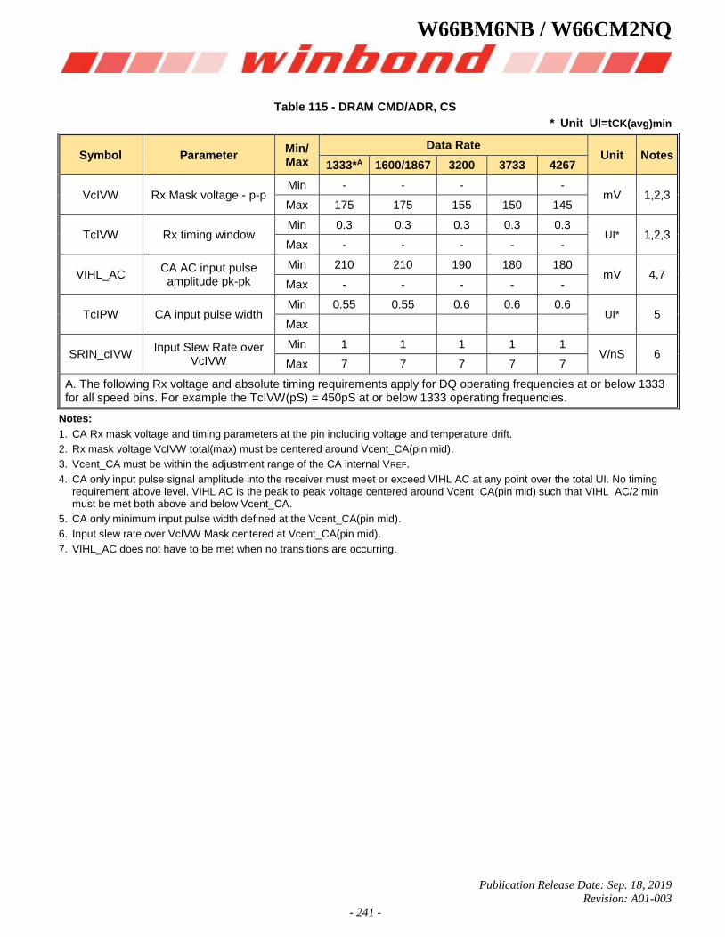
W66BM6NB / W66CM2NQ
Publication Release Date: Sep. 18, 2019
Revision: A01-003
- 241 -
Table 115 - DRAM CMD/ADR, CS
* Unit UI=tCK(avg)min
Symbol Parameter Min/Max
Data Rate Unit Notes
1333*A 1600/1867 3200 3733 4267
VcIVW Rx Mask voltage - p-p Min - - - -
mV 1,2,3 Max 175 175 155 150 145
TcIVW Rx timing window Min 0.3 0.3 0.3 0.3 0.3
UI* 1,2,3 Max - - - - -
VIHL_AC CA AC input pulse amplitude pk-pk
Min 210 210 190 180 180 mV 4,7
Max - - - - -
TcIPW CA input pulse width Min 0.55 0.55 0.6 0.6 0.6
UI* 5 Max
SRIN_cIVW Input Slew Rate over
VcIVW
Min 1 1 1 1 1 V/nS 6
Max 7 7 7 7 7
A. The following Rx voltage and absolute timing requirements apply for DQ operating frequencies at or below 1333 for all speed bins. For example the TcIVW(pS) = 450pS at or below 1333 operating frequencies.
Notes:
1. CA Rx mask voltage and timing parameters at the pin including voltage and temperature drift.
2. Rx mask voltage VcIVW total(max) must be centered around Vcent_CA(pin mid).
3. Vcent_CA must be within the adjustment range of the CA internal VREF.
4. CA only input pulse signal amplitude into the receiver must meet or exceed VIHL AC at any point over the total UI. No timing requirement above level. VIHL AC is the peak to peak voltage centered around Vcent_CA(pin mid) such that VIHL_AC/2 min must be met both above and below Vcent_CA.
5. CA only minimum input pulse width defined at the Vcent_CA(pin mid).
6. Input slew rate over VcIVW Mask centered at Vcent_CA(pin mid).
7. VIHL_AC does not have to be met when no transitions are occurring.
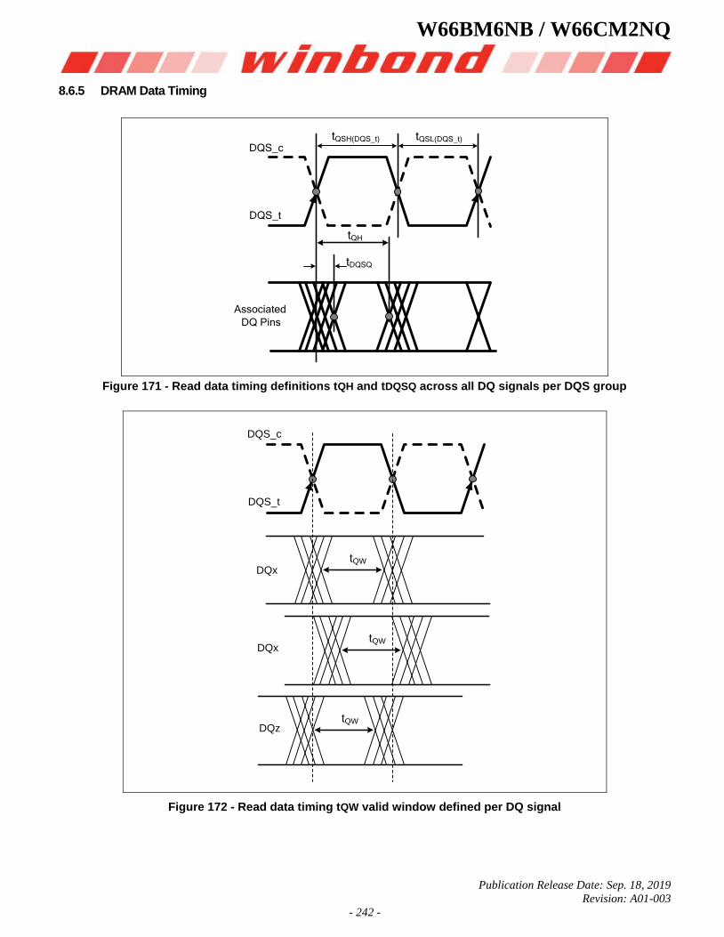
W66BM6NB / W66CM2NQ
Publication Release Date: Sep. 18, 2019
Revision: A01-003
- 242 -
8.6.5 DRAM Data Timing
Associated
DQ Pins
tDQSQ
tQH
tQSH(DQS_t) tQSL(DQS_t)
DQS_c
DQS_t
Figure 171 - Read data timing definitions tQH and tDQSQ across all DQ signals per DQS group
DQS_c
DQS_t
DQx
DQx
DQz
tQW
tQW
tQW
Figure 172 - Read data timing tQW valid window defined per DQ signal
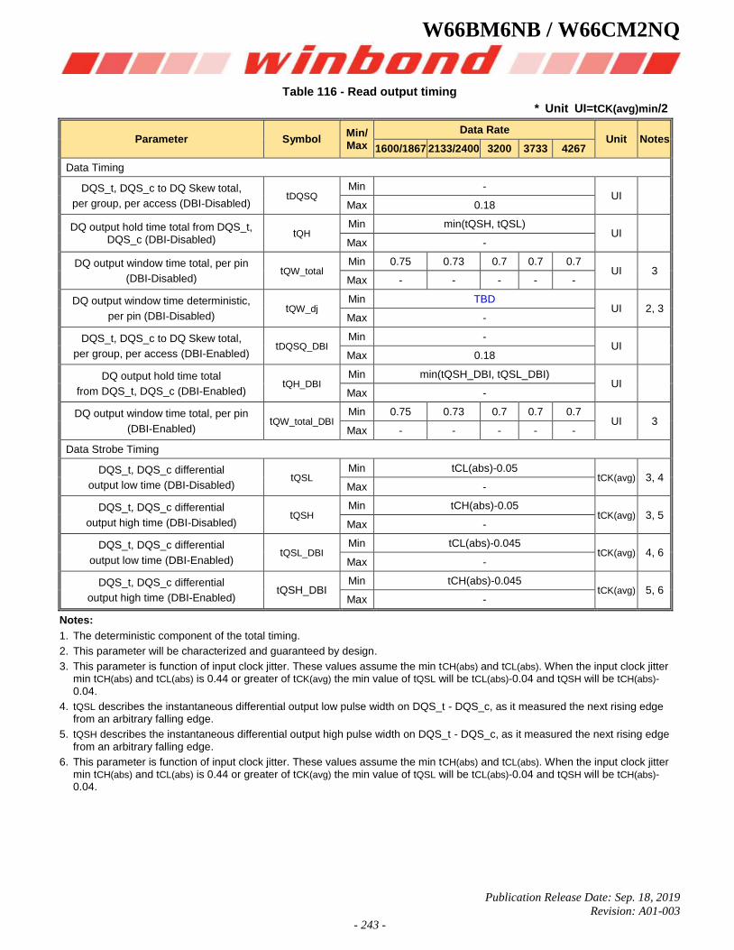
W66BM6NB / W66CM2NQ
Publication Release Date: Sep. 18, 2019
Revision: A01-003
- 243 -
Table 116 - Read output timing
* Unit UI=tCK(avg)min/2
Parameter Symbol Min/Max
Data Rate Unit Notes
1600/1867 2133/2400 3200 3733 4267
Data Timing
DQS_t, DQS_c to DQ Skew total,
per group, per access (DBI-Disabled) tDQSQ
Min - UI
Max 0.18
DQ output hold time total from DQS_t, DQS_c (DBI-Disabled)
tQH Min min(tQSH, tQSL)
UI Max -
DQ output window time total, per pin
(DBI-Disabled) tQW_total
Min 0.75 0.73 0.7 0.7 0.7 UI 3
Max - - - - -
DQ output window time deterministic,
per pin (DBI-Disabled) tQW_dj
Min TBD UI 2, 3
Max -
DQS_t, DQS_c to DQ Skew total,
per group, per access (DBI-Enabled) tDQSQ_DBI
Min - UI
Max 0.18
DQ output hold time total
from DQS_t, DQS_c (DBI-Enabled) tQH_DBI
Min min(tQSH_DBI, tQSL_DBI) UI
Max -
DQ output window time total, per pin
(DBI-Enabled) tQW_total_DBI
Min 0.75 0.73 0.7 0.7 0.7 UI 3
Max - - - - -
Data Strobe Timing
DQS_t, DQS_c differential
output low time (DBI-Disabled) tQSL
Min tCL(abs)-0.05 tCK(avg) 3, 4
Max -
DQS_t, DQS_c differential
output high time (DBI-Disabled) tQSH
Min tCH(abs)-0.05 tCK(avg) 3, 5
Max -
DQS_t, DQS_c differential
output low time (DBI-Enabled) tQSL_DBI
Min tCL(abs)-0.045 tCK(avg) 4, 6
Max -
DQS_t, DQS_c differential
output high time (DBI-Enabled) tQSH_DBI
Min tCH(abs)-0.045 tCK(avg) 5, 6
Max -
Notes:
1. The deterministic component of the total timing.
2. This parameter will be characterized and guaranteed by design.
3. This parameter is function of input clock jitter. These values assume the min tCH(abs) and tCL(abs). When the input clock jitter min tCH(abs) and tCL(abs) is 0.44 or greater of tCK(avg) the min value of tQSL will be tCL(abs)-0.04 and tQSH will be tCH(abs)-0.04.
4. tQSL describes the instantaneous differential output low pulse width on DQS_t - DQS_c, as it measured the next rising edge from an arbitrary falling edge.
5. tQSH describes the instantaneous differential output high pulse width on DQS_t - DQS_c, as it measured the next rising edge from an arbitrary falling edge.
6. This parameter is function of input clock jitter. These values assume the min tCH(abs) and tCL(abs). When the input clock jitter min tCH(abs) and tCL(abs) is 0.44 or greater of tCK(avg) the min value of tQSL will be tCL(abs)-0.04 and tQSH will be tCH(abs)-0.04.
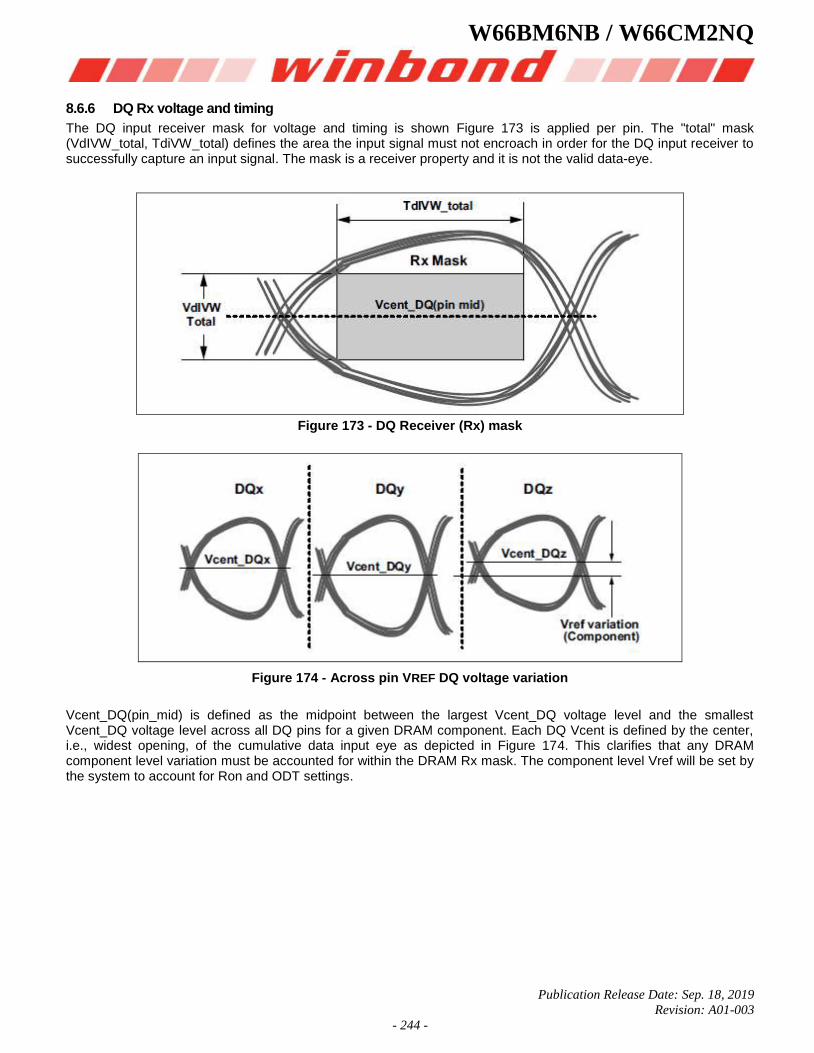
W66BM6NB / W66CM2NQ
Publication Release Date: Sep. 18, 2019
Revision: A01-003
- 244 -
8.6.6 DQ Rx voltage and timing
The DQ input receiver mask for voltage and timing is shown Figure 173 is applied per pin. The "total" mask (VdIVW_total, TdiVW_total) defines the area the input signal must not encroach in order for the DQ input receiver to successfully capture an input signal. The mask is a receiver property and it is not the valid data-eye.
Figure 173 - DQ Receiver (Rx) mask
Figure 174 - Across pin VREF DQ voltage variation
Vcent_DQ(pin_mid) is defined as the midpoint between the largest Vcent_DQ voltage level and the smallest Vcent_DQ voltage level across all DQ pins for a given DRAM component. Each DQ Vcent is defined by the center, i.e., widest opening, of the cumulative data input eye as depicted in Figure 174. This clarifies that any DRAM component level variation must be accounted for within the DRAM Rx mask. The component level Vref will be set by the system to account for Ron and ODT settings.
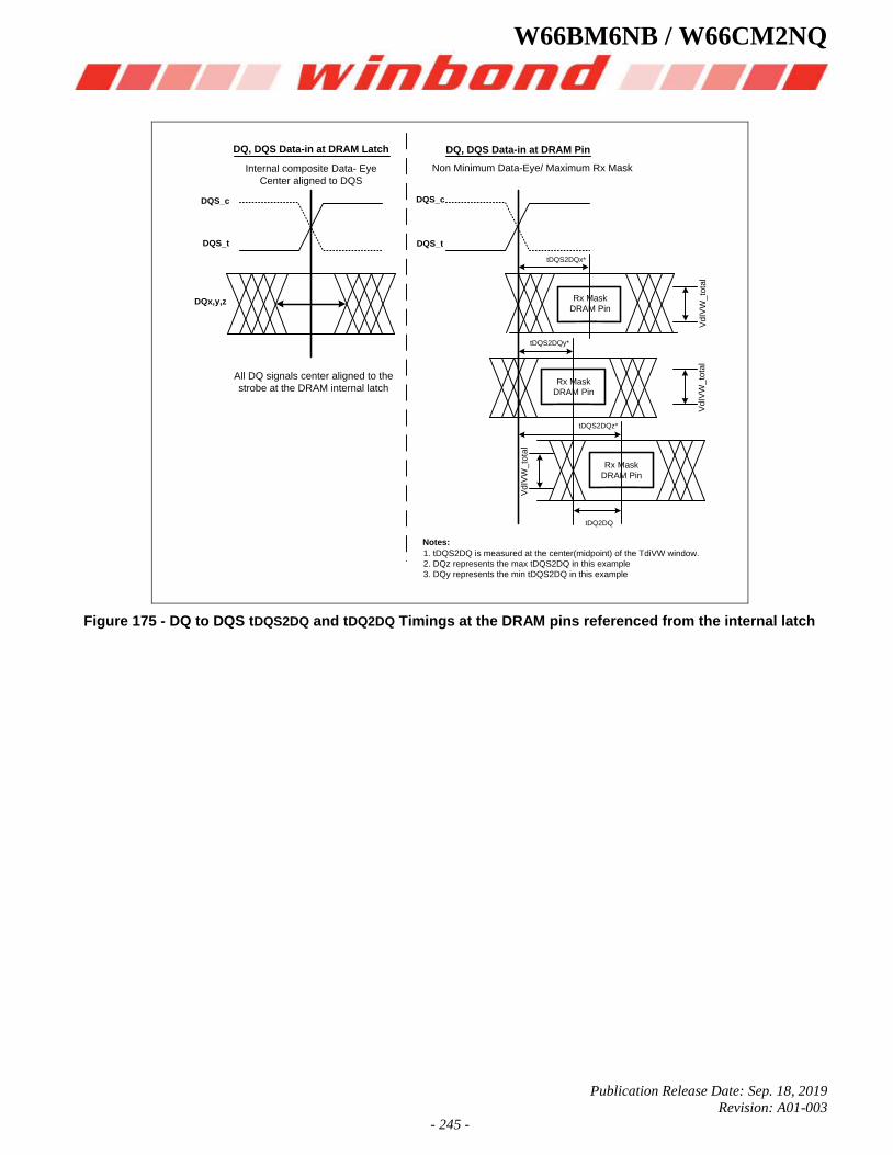
W66BM6NB / W66CM2NQ
Publication Release Date: Sep. 18, 2019
Revision: A01-003
- 245 -
DQS_t
DQS_c
DQ, DQS Data-in at DRAM Latch DQ, DQS Data-in at DRAM Pin
Non Minimum Data-Eye/ Maximum Rx MaskInternal composite Data- Eye
Center aligned to DQS
DQS_t
DQS_c
DQx,y,z
All DQ signals center aligned to the
strobe at the DRAM internal latch
tDQS2DQx*
tDQS2DQy*
tDQS2DQz*
tDQ2DQ
Rx Mask
DRAM Pin
Rx Mask
DRAM Pin
Rx Mask
DRAM Pin
Vd
IVW
_to
tal
Vd
IVW
_to
tal
Notes:
1. tDQS2DQ is measured at the center(midpoint) of the TdiVW window.
2. DQz represents the max tDQS2DQ in this example
3. DQy represents the min tDQS2DQ in this example
Vd
IVW
_to
tal
Figure 175 - DQ to DQS tDQS2DQ and tDQ2DQ Timings at the DRAM pins referenced from the internal latch
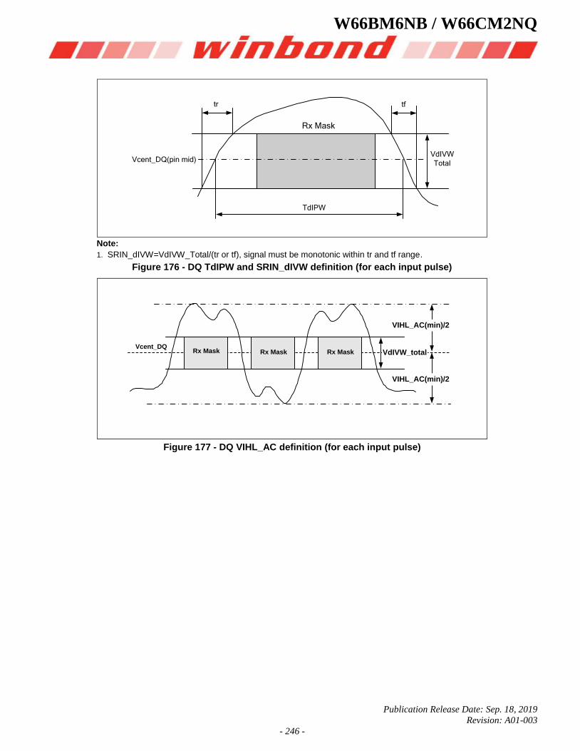
W66BM6NB / W66CM2NQ
Publication Release Date: Sep. 18, 2019
Revision: A01-003
- 246 -
Rx Mask
TdIPW
tr tf
Vcent_DQ(pin mid)VdIVW
Total
Note:
1. SRIN_dIVW=VdIVW_Total/(tr or tf), signal must be monotonic within tr and tf range.
Figure 176 - DQ TdIPW and SRIN_dIVW definition (for each input pulse)
VIHL_AC(min)/2
VIHL_AC(min)/2
Vcent_DQRx Mask Rx MaskRx Mask VdIVW_total
Figure 177 - DQ VIHL_AC definition (for each input pulse)
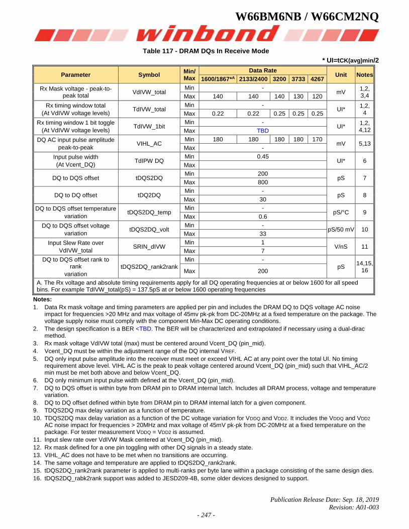
W66BM6NB / W66CM2NQ
Publication Release Date: Sep. 18, 2019
Revision: A01-003
- 247 -
Table 117 - DRAM DQs In Receive Mode
* UI=tCK(avg)min/2
Parameter Symbol Min/Max
Data Rate Unit Notes
1600/1867*A 2133/2400 3200 3733 4267
Rx Mask voltage - peak-to-peak total
VdIVW_total Min -
mV 1,2,3,4 Max 140 140 140 130 120
Rx timing window total
(At VdIVW voltage levels) TdIVW_total
Min - UI*
1,2,4 Max 0.22 0.22 0.25 0.25 0.25
Rx timing window 1 bit toggle
(At VdIVW voltage levels) TdIVW_1bit
Min - UI*
1,2,4,12 Max TBD
DQ AC input pulse amplitude
peak-to-peak VIHL_AC
Min 180 180 180 180 170 mV 5,13
Max -
Input pulse width
(At Vcent_DQ) TdIPW DQ
Min 0.45 UI* 6
Max
DQ to DQS offset tDQS2DQ Min 200
pS 7 Max 800
DQ to DQ offset tDQ2DQ Min -
pS 8 Max 30
DQ to DQS offset temperature
variation tDQS2DQ_temp
Min - pS/°C 9
Max 0.6
DQ to DQS offset voltage
variation tDQS2DQ_volt
Min - pS/50 mV 10
Max 33
Input Slew Rate over
VdIVW_total SRIN_dIVW
Min 1 V/nS 11
Max 7
DQ to DQS offset rank to rank
variation
tDQS2DQ_rank2rank
Min -
pS 14,15,
16 Max 200
A. The Rx voltage and absolute timing requirements apply for all DQ operating frequencies at or below 1600 for all speed bins. For example TdIVW_total(pS) = 137.5pS at or below 1600 operating frequencies
Notes:
1. Data Rx mask voltage and timing parameters are applied per pin and includes the DRAM DQ to DQS voltage AC noise impact for frequencies >20 MHz and max voltage of 45mv pk-pk from DC-20MHz at a fixed temperature on the package. The voltage supply noise must comply with the component Min-Max DC operating conditions.
2. The design specification is a BER <TBD. The BER will be characterized and extrapolated if necessary using a dual-dirac method.
3. Rx mask voltage VdIVW total (max) must be centered around Vcent_DQ (pin_mid).
4. Vcent_DQ must be within the adjustment range of the DQ internal VREF.
5. DQ only input pulse amplitude into the receiver must meet or exceed VIHL AC at any point over the total UI. No timing requirement above level. VIHL AC is the peak to peak voltage centered around Vcent_DQ (pin_mid) such that VIHL_AC/2 min must be met both above and below Vcent_DQ.
6. DQ only minimum input pulse width defined at the Vcent_DQ (pin_mid).
7. DQ to DQS offset is within byte from DRAM pin to DRAM internal latch. Includes all DRAM process, voltage and temperature variation.
8. DQ to DQ offset defined within byte from DRAM pin to DRAM internal latch for a given component.
9. TDQS2DQ max delay variation as a function of temperature.
10. TDQS2DQ max delay variation as a function of the DC voltage variation for VDDQ and VDD2. It includes the VDDQ and VDD2 AC noise impact for frequencies > 20MHz and max voltage of 45mV pk-pk from DC-20MHz at a fixed temperature on the package. For tester measurement VDDQ = VDD2 is assumed.
11. Input slew rate over VdIVW Mask centered at Vcent_DQ (pin_mid).
12. Rx mask defined for a one pin toggling with other DQ signals in a steady state.
13. VIHL_AC does not have to be met when no transitions are occurring.
14. The same voltage and temperature are applied to tDQS2DQ_rank2rank.
15. tDQS2DQ_rank2rank parameter is applied to multi-ranks per byte lane within a package consisting of the same design dies.
16. tDQS2DQ_rabk2rank support was added to JESD209-4B, some older devices designed to support.
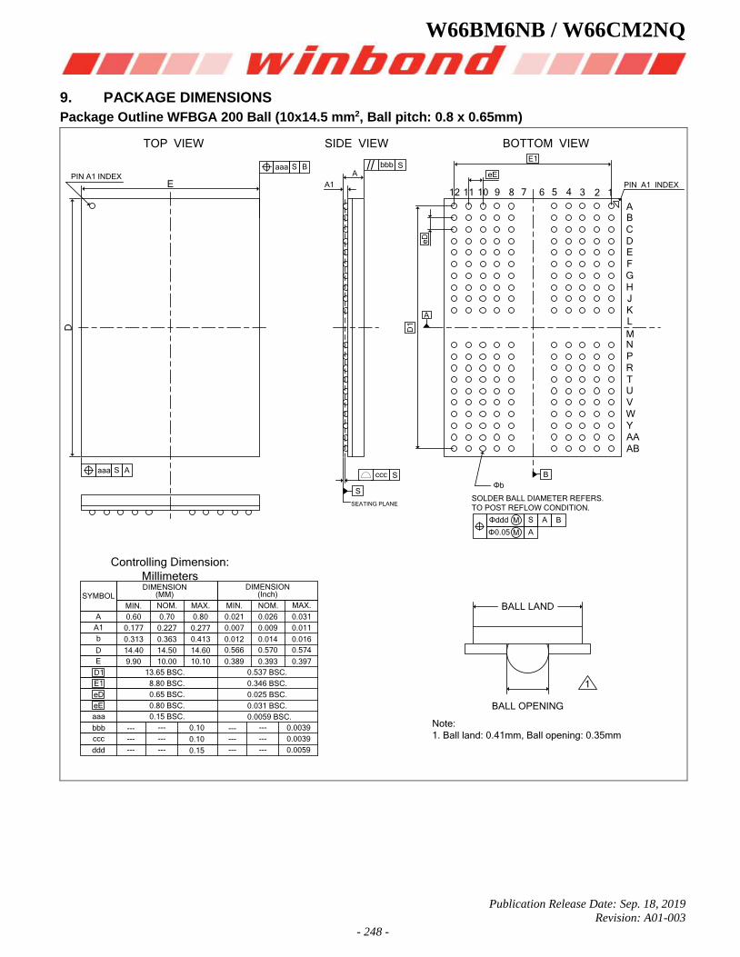
W66BM6NB / W66CM2NQ
Publication Release Date: Sep. 18, 2019
Revision: A01-003
- 248 -
9. PACKAGE DIMENSIONS
Package Outline WFBGA 200 Ball (10x14.5 mm2, Ball pitch: 0.8 x 0.65mm)
A1
A
12
A
Sccc
S
Sbbb//
345678910
S A BΦddd M
Φb
SOLDER BALL DIAMETER REFERS.
TO POST REFLOW CONDITION.SEATING PLANE
B
A
PIN A1 INDEX
D1
eD
E1
eE
Note:
1. Ball land: 0.41mm, Ball opening: 0.35mm
BALL LAND
BALL OPENING
1
B
C
DE
F
G
HJ
KL
MN
P
R
TU
V
W
Y
AA
AB
1112
AΦ0.05 M
D
EPIN A1 INDEX
S Aaaa
S Baaa
BOTTOM VIEWTOP VIEW SIDE VIEW
SYMBOL
MIN. NOM. MAX.
A
A1
b
D
E
aaa
bbb
ccc
ddd
--- ---
--- ---
--- --- 0.15
0.10
0.10
0.80 BSC.
0.65 BSC.
8.80 BSC.
13.65 BSC.
0.80
0.277
0.413
14.60
10.1010.00
14.50
9.90
14.40
0.313
0.177
MIN. NOM. MAX.
--- ---
--- ---
--- ---
0.031 BSC.
0.025 BSC.
0.346 BSC.
0.537 BSC.
0.031
0.011
0.016
0.574
0.397
0.007
0.012
0.566
0.389
0.570
0.393
0.0039
0.0039
0.0059
0.363
Controlling Dimension:
MillimetersDIMENSION
(MM)DIMENSION
(Inch)
eE
eD
E1
D1
0.15 BSC. 0.0059 BSC.
0.60 0.70
0.227
0.021 0.026
0.009
0.014
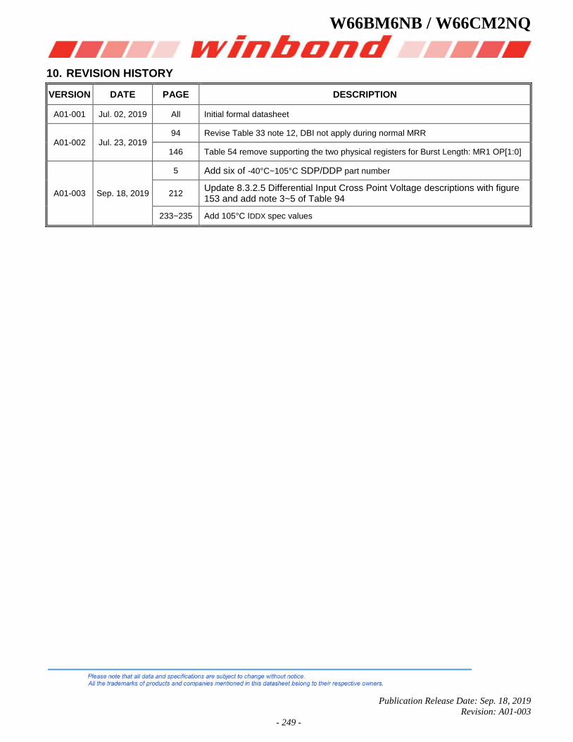
W66BM6NB / W66CM2NQ
Publication Release Date: Sep. 18, 2019
Revision: A01-003
- 249 -
10. REVISION HISTORY
VERSION DATE PAGE DESCRIPTION
A01-001 Jul. 02, 2019 All Initial formal datasheet
A01-002 Jul. 23, 2019 94 Revise Table 33 note 12, DBI not apply during normal MRR
146 Table 54 remove supporting the two physical registers for Burst Length: MR1 OP[1:0]
A01-003 Sep. 18, 2019
5 Add six of -40°C~105°C SDP/DDP part number
212 Update 8.3.2.5 Differential Input Cross Point Voltage descriptions with figure 153 and add note 3~5 of Table 94
233~235 Add 105°C IDDX spec values


![USER GUIDE - Winbond€¦ · USER GUIDE Winbond Flash Memory Sample Shield [1] Publication Date: December 4, 2017 Revision 2.0 1. INTRODUCTION This describes how to use the Winbond](https://img.pdfslide.net/doc/110x75/5ee196d2ad6a402d666c69bb/user-guide-winbond-user-guide-winbond-flash-memory-sample-shield-1-publication.jpg)