Embed Size (px)
Citation preview
WGM160P Wi-Fi® Module Data Sheet
The WGM160P is an ultra low power standalone Wi-Fi® module targeted for applicationsrequiring superior RF performance in noisy environments, low power consumption, highsecurity, integrated customer applications and fast time to market.
The WGM160P module integrates all of the necessary elements required for a cloudconnected IoT Wi-Fi application, including 802.11b/g/n radio, integrated chip antenna,certifications, microcontroller, Wi-Fi and IP stacks, HTTP server, and multiple protocols,such as TCP and UDP. Co-existence with external 2.4GHz transceivers is supported.
WGM160P can be configured to concurrently act as a Wi-Fi client and a Wi-Fi accesspoint, which is ideal for user friendly device provisioning. WGM160P can natively host C-applications, removing the need for an external host controller. Alternatively, the Wi-FiModule can run in Network Co-Processor (NCP) mode, leaving the complexity of TCP/IPnetworking to the module so that the customer’s own host controller can be fully dedica-ted to processing the customer application tasks. The WGM160P module has highlyflexible host and peripheral hardware interfaces for wide application use.
This module also supports Gecko OS, a comprehensive software suite designed to sim-plify your Wi-Fi, application, device management and cloud connectivity developmentprocess.
KEY POINTS
• Available with integrated chip antenna oran RF pin
• Antenna diversity supported via secondaryRF pin
• IEEE 802.11 b/g/n compliant• TX power: +16 dBm• RX sensitivity: -95.5 dBm• CPU core: 32-bit ARM® Cortex-M4• Flash memory: 2 MB• RAM: 512 kB• Concurrent mode: Wi-Fi AP and STA• Ultra low power consumption• Modular certification
• CE, FCC, ISED• Japan, KC
• End-to-end security• Built-in 10/100 Ethernet Support• Gecko OS support• Size: 23.8 mm x 14.2 mm x 2.3 mm
32-bit bus
Lowest power mode with peripheral operational:
EM2 – Deep SleepEM1 - Sleep EM4H - Hibernate EM4S - ShutoffEM0 - Active EM3 - Stop
Core / Memory
Flash Program Memory
RAM Memory
ARM CortexTM M4 processor with FPU and
MPU
Debug Interface
LDMA Controller
ETM
Other
CRYPTO
CRC
Energy Management
Brown-Out Detector
DC-DC Converter
Voltage Regulator
Voltage/Temp Monitor
Power-On Reset
Clock ManagementHigh Frequency
RC Oscillator
Ultra Low Freq. RC Oscillator
Universal HF RC Oscillator
Low Frequency XTAL + Oscillator
Low FrequencyRC Oscillator
Auxiliary High Freq. RC Osc.
High Frequency Crystal Oscillator
PLL
Analog Interfaces
Low Energy LCD Controller
IDAC
Operational Amplifier
ADC
VDAC
Analog Comparator
Capacitive Sensing
Backup Domain
Peripheral Reflex System
Serial Interfaces
UART
I2CLEUSB(crystal free)
I/O Ports Timers and TriggersLow Energy Sensor IFTimer/Counter
Low Energy Timer
Watchdog Timer
CRYOTIMER
External Interrupts
Pin Reset
General Purpose I/O
Pin Wakeup
Real Time Counter and Calendar
Pulse Counter
Real Time CounterQuad-SPI
USART
Low Energy UARTTMCAN
10/100 Ethernet
True Random Number Generator
SMU
Wi-Fi Radio
2.4 GHz Transceiver
Diversity Input
802.11 b/g/n MODEM
PTA support
Certified Module
Antenna
Radio XTAL
Matching
silabs.com | Building a more connected world. Rev. 1.0
1. Key Features
The key features of the WGM160P module are listed below.Radio Features• Built-in Antenna (optional)• TX Power: +16 dBm• RX Sensitivity: -95.5 dBm• Superior blocking performance
Wi-Fi Features• 802.11: b/g/n• Bit rate: up to 72.2 Mbps• 802.11 Security: WPA2/WPA Personal• STA (Station Mode)• SoftAP (Soft Access Point Mode)
Electrical Characteristics• Supply voltage: 3.0V to 3.6V
Environmental Specifications• Temperature range: -40°C to +85°C
Modular Certification• CE, FCC, ISED, KC, Japan• RoHS/REACH compliant
Dimensions• L x W x H: 23.8 mm x 14.2 mm x 2.3 mm
MCU Features
• ARM® Cortex-M4, 72MHz• 512 kB RAM• 2 MB Flash
Hardware Interfaces
• Host interface: UART/SPI/USB• Peripheral interfaces
• 2 x USART (UART/SPI/I2S)• QSPI with Execute In Place (XIP) support• SD Card support (SPI)• Capacitive Touch Sensing in all GPIOs• LESENSE• 10/100 Ethernet MAC with RMII interface• USB device (2.0 Full speed)• I2C peripheral interfaces• CAN
• Up to 31 x GPIO with interrupts• 2 x 12-bit ADC• 2 x 12-bit DAC• Rich selection of timers, inc. Real-time counters• Co-existence interface (PTA: 2, 3, 4 wire)
WGM160P Wi-Fi® Module Data SheetKey Features
silabs.com | Building a more connected world. Rev. 1.0 | 2
2. Ordering Information
Table 2.1. Ordering Information
Part Number Protocol Max TXPower
Flash/Ram(kB)
LF XTAL Antenna GPIO Carrier
WGM160PX22KGA2 Wi-Fi (802.11 b/g/n) 16 dBm 2048 / 512 Included Built-in Up to 31 Cut Tape
WGM160PX22KGA2R Wi-Fi (802.11 b/g/n) 16 dBm 2048 / 512 Included Built-in Up to 31 Reel
WGM160P022KGA2 Wi-Fi (802.11 b/g/n) 16 dBm 2048 / 512 None Built-in Up to 31 Cut Tape
WGM160P022KGA2R Wi-Fi (802.11 b/g/n) 16 dBm 2048 / 512 None Built-in Up to 31 Reel
WGM160PX22KGN2 Wi-Fi (802.11 b/g/n) 16 dBm 2048 / 512 Included External (RF Pin) Up to 31 Cut Tape
WGM160PX22KGN2R Wi-Fi (802.11 b/g/n) 16 dBm 2048 / 512 Included External (RF Pin) Up to 31 Reel
WGM160P022KGN2 Wi-Fi (802.11 b/g/n) 16 dBm 2048 / 512 None External (RF Pin) Up to 31 Cut Tape
WGM160P022KGN2R Wi-Fi (802.11 b/g/n) 16 dBm 2048 / 512 None External (RF Pin) Up to 31 Reel
Note:1. WGM160P modules come pre-programmed with the Gecko OS Kernel. Devices ship with the debug interface locked. Devices may
be reprogrammed via serial or OTA DFU and preserve the device credentials. Unlocking the debug interface will result in loss ofpre-programmed firmware, including Gecko OS Kernel and device credentials.
2. SLWSTK6121A Wireless Starter Kit and SLWRB4321A Radio Board are available to start developing with WGM160P Wi-Fi mod-ules.
3. Devices listed may be referred to by the product family name (WGM160P), model name (WGM160P22A / WGM160P22N) or thefull orderable part number throughout this document.
WGM160P Wi-Fi® Module Data SheetOrdering Information
silabs.com | Building a more connected world. Rev. 1.0 | 3
Table of Contents1. Key Features . . . . . . . . . . . . . . . . . . . . . . . . . . . . . . . 2
2. Ordering Information . . . . . . . . . . . . . . . . . . . . . . . . . . . . 3
3. System Overview . . . . . . . . . . . . . . . . . . . . . . . . . . . . . . 63.1 Introduction . . . . . . . . . . . . . . . . . . . . . . . . . . . . . . . 6
3.2 Wi-Fi Supported 2.4 GHz ISM Modulations, BW, and Channels . . . . . . . . . . . . . 6
4. Electrical Specifications . . . . . . . . . . . . . . . . . . . . . . . . . . . 74.1 Absolute Maximum Ratings. . . . . . . . . . . . . . . . . . . . . . . . . . 7
4.2 Operating Conditions . . . . . . . . . . . . . . . . . . . . . . . . . . . . 8
4.3 Power Consumption . . . . . . . . . . . . . . . . . . . . . . . . . . . . 8
4.4 Digital I/O Specifications. . . . . . . . . . . . . . . . . . . . . . . . . . . 9
4.5 RF Transmitter General Characteristics . . . . . . . . . . . . . . . . . . . . .10
4.6 RF Receiver General Characteristics . . . . . . . . . . . . . . . . . . . . . .11
4.7 Radiated Characteristics. . . . . . . . . . . . . . . . . . . . . . . . . . .11
4.8 Microcontroller Peripherals . . . . . . . . . . . . . . . . . . . . . . . . . .12
5. Typical Applications and Connections . . . . . . . . . . . . . . . . . . . . . 135.1 RF Connections . . . . . . . . . . . . . . . . . . . . . . . . . . . . .13
5.1.1 Antenna Ports . . . . . . . . . . . . . . . . . . . . . . . . . . . . .135.1.2 Antenna Diversity . . . . . . . . . . . . . . . . . . . . . . . . . . .13
5.2 Multi-Protocol Coexistence . . . . . . . . . . . . . . . . . . . . . . . . . .13
5.3 Example Schematic . . . . . . . . . . . . . . . . . . . . . . . . . . . .14
6. Gecko OS Features . . . . . . . . . . . . . . . . . . . . . . . . . . . . 15
7. Pin Descriptions . . . . . . . . . . . . . . . . . . . . . . . . . . . . . 167.1 WGM160P Device Pinout . . . . . . . . . . . . . . . . . . . . . . . . . .16
7.2 GPIO Functionality . . . . . . . . . . . . . . . . . . . . . . . . . . . .18
7.3 Alternate Pin Functionality . . . . . . . . . . . . . . . . . . . . . . . . . .22
8. Package Specifications . . . . . . . . . . . . . . . . . . . . . . . . . . 328.1 Package Outline . . . . . . . . . . . . . . . . . . . . . . . . . . . . .32
8.2 Recommended PCB Land Patterns . . . . . . . . . . . . . . . . . . . . . . .33
8.3 Package Marking . . . . . . . . . . . . . . . . . . . . . . . . . . . . .35
9. Soldering Recommendations . . . . . . . . . . . . . . . . . . . . . . . . 36
10. Tape and Reel Dimensions . . . . . . . . . . . . . . . . . . . . . . . . . 37
11. Certifications . . . . . . . . . . . . . . . . . . . . . . . . . . . . . . 3811.1 Qualified External Antenna Types . . . . . . . . . . . . . . . . . . . . . . .38
11.2 CE . . . . . . . . . . . . . . . . . . . . . . . . . . . . . . . . .38
silabs.com | Building a more connected world. Rev. 1.0 | 4

11.3 FCC . . . . . . . . . . . . . . . . . . . . . . . . . . . . . . . . .39
11.4 ISED Canada . . . . . . . . . . . . . . . . . . . . . . . . . . . . . .40
11.5 Locating the Module Close to Human Body . . . . . . . . . . . . . . . . . . . .42
11.6 Japan . . . . . . . . . . . . . . . . . . . . . . . . . . . . . . . .43
11.7 KC South Korea . . . . . . . . . . . . . . . . . . . . . . . . . . . . .43
12. Revision History. . . . . . . . . . . . . . . . . . . . . . . . . . . . . 44
silabs.com | Building a more connected world. Rev. 1.0 | 5
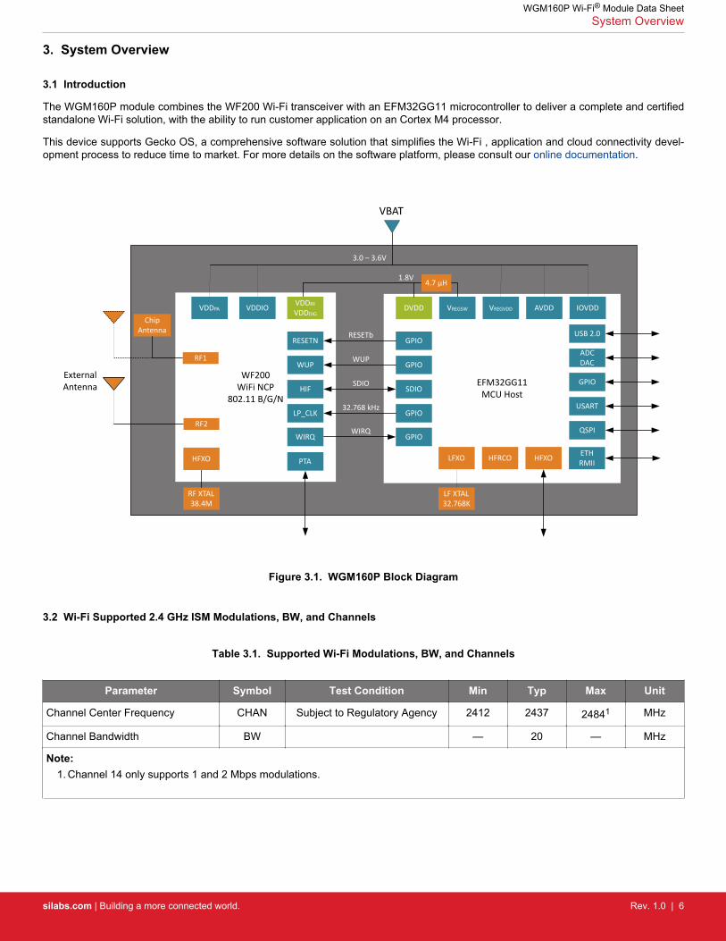
3. System Overview
3.1 Introduction
The WGM160P module combines the WF200 Wi-Fi transceiver with an EFM32GG11 microcontroller to deliver a complete and certifiedstandalone Wi-Fi solution, with the ability to run customer application on an Cortex M4 processor.
This device supports Gecko OS, a comprehensive software solution that simplifies the Wi-Fi , application and cloud connectivity devel-opment process to reduce time to market. For more details on the software platform, please consult our online documentation.
WF200WiFi NCP
802.11 B/G/N
ChipAntenna
RF XTAL38.4M
External Antenna EFM32GG11
MCU Host
GPIO
LF XTAL32.768K
LFXOHFXO
RESETb
WUP
SDIO
32.768 kHz
VDDPA VDDIO
1.8V
RF1
RF2
DVDD VREGVDDVREGSW AVDD IOVDD
4.7 µH
GPIO
SDIO
GPIO
RESETN
WUP
HIF
LP_CLK
USB 2.0
ADCDAC
GPIO
USART
QSPI
HFRCOPTA HFXO ETH RMII
WIRQGPIOWIRQ
VDDRF
VDDDIG
VBAT
3.0 – 3.6V
Figure 3.1. WGM160P Block Diagram
3.2 Wi-Fi Supported 2.4 GHz ISM Modulations, BW, and Channels
Table 3.1. Supported Wi-Fi Modulations, BW, and Channels
Parameter Symbol Test Condition Min Typ Max Unit
Channel Center Frequency CHAN Subject to Regulatory Agency 2412 2437 24841 MHz
Channel Bandwidth BW — 20 — MHz
Note:1. Channel 14 only supports 1 and 2 Mbps modulations.
WGM160P Wi-Fi® Module Data SheetSystem Overview
silabs.com | Building a more connected world. Rev. 1.0 | 6
4. Electrical Specifications
All electrical parameters in all tables are specified under the following conditions, unless stated otherwise:• Typical values are based on TAMB = 25 °C; VVBAT = 3.3V; Center Frequency = 2,437 MHz.• Radio performance numbers are measured in conducted mode, based on Silicon Laboratories reference designs using output pow-
er-specific external RF impedance-matching networks for interfacing to a 50 Ω antenna port. Conducted RF measurements includeadditional output power reductions to guarantee WiFi and regulatory emissions compliance while connected to the specified anten-nas which have non-ideal impedance loading.
Refer to Section 4.2 Operating Conditions for more details about operational supply and temperature limits.
4.1 Absolute Maximum Ratings
Stresses above those listed below may cause permanent damage to the device. This is a stress rating only and functional operation ofthe devices at those or any other conditions above those indicated in the operation listings of this specification is not implied. Exposureto maximum rating conditions for extended periods may affect device reliability. For more information on the available quality and relia-bility data, see the Quality and Reliability Monitor Report at http://www.silabs.com/support/quality/pages/default.aspx.
Table 4.1. Absolute Maximum Ratings
Parameter Symbol Test Condition Min Typ Max Unit
Storage temperature TSTG -40 — 105 °C
RF power level at RF1 andRF2 ports
PRFMAX Max power that can be applied toinput of recommended matchingnetwork connected to RF1 andRF2 pins.
— — 10 dBm
Maximum supply voltage toVBAT
VBATMAX -0.3 — 3.6 V
DC voltage on I/O pins VGMAX 5 V tolerant GPIO (PF0, PF1,PF10, PF11)1 2
-0.3 — Min of 5.25and VBAT
+2
V
All other GPIO and PTA pins -0.3 — VBAT + 0.3 V
Current into any GPIO pin IOMAX — — 20 mA
Sum of current into all GPIOpins
IOALL_MAX — — 150 mA
Range of load impedance atRF1 and RF2 pins during TX
LOADTX — — 10:1 VSWR
Note:1. When a GPIO is used for analog functions via the APORT, the maximum voltage is VBAT.2. To operate above the VBAT supply rail, over-voltage tolerance must be enabled according to the GPIO_Px_OVTDIS register.
Pins with over-voltage tolerance disabled have the same limits as all other GPIO (max = VBAT + 0.3 V).
WGM160P Wi-Fi® Module Data SheetElectrical Specifications
silabs.com | Building a more connected world. Rev. 1.0 | 7
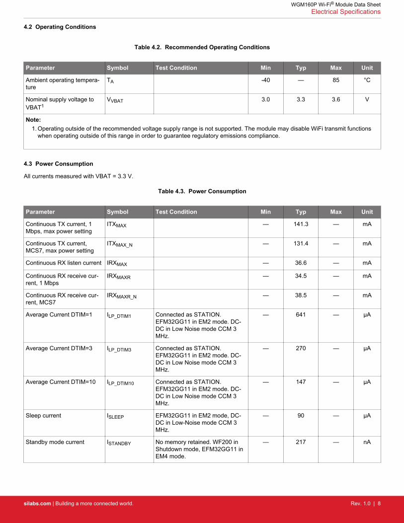
4.2 Operating Conditions
Table 4.2. Recommended Operating Conditions
Parameter Symbol Test Condition Min Typ Max Unit
Ambient operating tempera-ture
TA -40 — 85 °C
Nominal supply voltage toVBAT1
VVBAT 3.0 3.3 3.6 V
Note:1. Operating outside of the recommended voltage supply range is not supported. The module may disable WiFi transmit functions
when operating outside of this range in order to guarantee regulatory emissions compliance.
4.3 Power Consumption
All currents measured with VBAT = 3.3 V.
Table 4.3. Power Consumption
Parameter Symbol Test Condition Min Typ Max Unit
Continuous TX current, 1Mbps, max power setting
ITXMAX — 141.3 — mA
Continuous TX current,MCS7, max power setting
ITXMAX_N — 131.4 — mA
Continuous RX listen current IRXMAX — 36.6 — mA
Continuous RX receive cur-rent, 1 Mbps
IRXMAXR — 34.5 — mA
Continuous RX receive cur-rent, MCS7
IRXMAXR_N — 38.5 — mA
Average Current DTIM=1 ILP_DTIM1 Connected as STATION.EFM32GG11 in EM2 mode. DC-DC in Low Noise mode CCM 3MHz.
— 641 — µA
Average Current DTIM=3 ILP_DTIM3 Connected as STATION.EFM32GG11 in EM2 mode. DC-DC in Low Noise mode CCM 3MHz.
— 270 — µA
Average Current DTIM=10 ILP_DTIM10 Connected as STATION.EFM32GG11 in EM2 mode. DC-DC in Low Noise mode CCM 3MHz.
— 147 — µA
Sleep current ISLEEP EFM32GG11 in EM2 mode, DC-DC in Low-Noise mode CCM 3MHz.
— 90 — µA
Standby mode current ISTANDBY No memory retained. WF200 inShutdown mode, EFM32GG11 inEM4 mode.
— 217 — nA
WGM160P Wi-Fi® Module Data SheetElectrical Specifications
silabs.com | Building a more connected world. Rev. 1.0 | 8
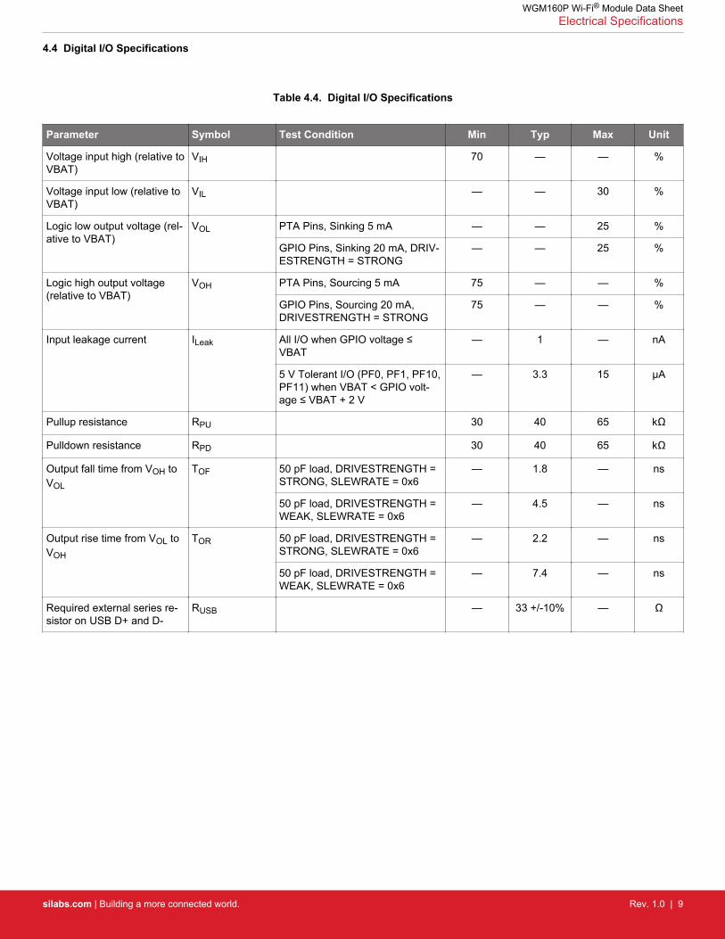
4.4 Digital I/O Specifications
Table 4.4. Digital I/O Specifications
Parameter Symbol Test Condition Min Typ Max Unit
Voltage input high (relative toVBAT)
VIH 70 — — %
Voltage input low (relative toVBAT)
VIL — — 30 %
Logic low output voltage (rel-ative to VBAT)
VOL PTA Pins, Sinking 5 mA — — 25 %
GPIO Pins, Sinking 20 mA, DRIV-ESTRENGTH = STRONG
— — 25 %
Logic high output voltage(relative to VBAT)
VOH PTA Pins, Sourcing 5 mA 75 — — %
GPIO Pins, Sourcing 20 mA,DRIVESTRENGTH = STRONG
75 — — %
Input leakage current ILeak All I/O when GPIO voltage ≤VBAT
— 1 — nA
5 V Tolerant I/O (PF0, PF1, PF10,PF11) when VBAT < GPIO volt-age ≤ VBAT + 2 V
— 3.3 15 µA
Pullup resistance RPU 30 40 65 kΩ
Pulldown resistance RPD 30 40 65 kΩ
Output fall time from VOH toVOL
TOF 50 pF load, DRIVESTRENGTH =STRONG, SLEWRATE = 0x6
— 1.8 — ns
50 pF load, DRIVESTRENGTH =WEAK, SLEWRATE = 0x6
— 4.5 — ns
Output rise time from VOL toVOH
TOR 50 pF load, DRIVESTRENGTH =STRONG, SLEWRATE = 0x6
— 2.2 — ns
50 pF load, DRIVESTRENGTH =WEAK, SLEWRATE = 0x6
— 7.4 — ns
Required external series re-sistor on USB D+ and D-
RUSB — 33 +/-10% — Ω
WGM160P Wi-Fi® Module Data SheetElectrical Specifications
silabs.com | Building a more connected world. Rev. 1.0 | 9
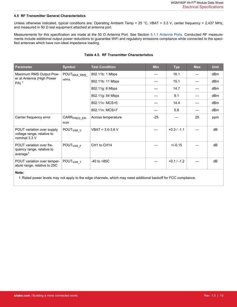
4.5 RF Transmitter General Characteristics
Unless otherwise indicated, typical conditions are: Operating Ambient Temp = 25 °C, VBAT = 3.3 V, center frequency = 2,437 MHz,and measured in 50 Ω test equipment attached at antenna port.
Measurements for this specification are made at the 50 Ω Antenna Port. See Section 5.1.1 Antenna Ports. Conducted RF measure-ments include additional output power reductions to guarantee WiFi and regulatory emissions compliance while connected to the speci-fied antennas which have non-ideal impedance loading.
Table 4.5. RF Transmitter Characteristics
Parameter Symbol Test Condition Min Typ Max Unit
Maximum RMS Output Pow-er at Antenna (High PowerPA) 1
POUTMAX_RMS_
HPPA
802.11b: 1 Mbps — 16.1 — dBm
802.11b: 11 Mbps — 15.1 — dBm
802.11g: 6 Mbps — 14.7 — dBm
802.11g: 54 Mbps — 9.1 — dBm
802.11n: MCS=0 — 14.4 — dBm
802.11n: MCS=7 — 5.8 — dBm
Carrier frequency error CARRFREQ_ER-
ROR
Across temperature -25 — 25 ppm
POUT variation over supplyvoltage range, relative tonominal 3.3 V
POUTVAR_V VBAT = 3.0-3.6 V — +0.3 / -1.1 — dB
POUT variation over fre-quency range, relative toaverage1
POUTVAR_F CH1 to CH14 — +/-0.15 — dB
POUT variation over temper-ature range, relative to 25C
POUTVAR_T -40 to +85C — +0.1 / -1.2 — dB
Note:1. Rated power levels may not apply to the edge channels, which may need additional backoff for FCC compliance.
WGM160P Wi-Fi® Module Data SheetElectrical Specifications
silabs.com | Building a more connected world. Rev. 1.0 | 10
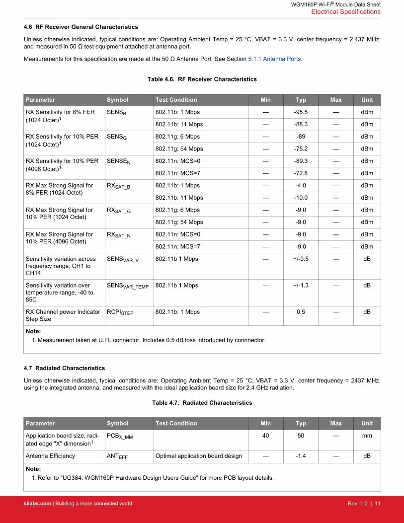
4.6 RF Receiver General Characteristics
Unless otherwise indicated, typical conditions are: Operating Ambient Temp = 25 °C, VBAT = 3.3 V, center frequency = 2,437 MHz,and measured in 50 Ω test equipment attached at antenna port.
Measurements for this specification are made at the 50 Ω Antenna Port. See Section 5.1.1 Antenna Ports.
Table 4.6. RF Receiver Characteristics
Parameter Symbol Test Condition Min Typ Max Unit
RX Sensitivity for 8% FER(1024 Octet)1
SENSB 802.11b: 1 Mbps — -95.5 — dBm
802.11b: 11 Mbps — -88.3 — dBm
RX Sensitivity for 10% PER(1024 Octet)1
SENSG 802.11g: 6 Mbps — -89 — dBm
802.11g: 54 Mbps — -75.2 — dBm
RX Sensitivity for 10% PER(4096 Octet)1
SENSEN 802.11n: MCS=0 — -89.3 — dBm
802.11n: MCS=7 — -72.8 — dBm
RX Max Strong Signal for8% FER (1024 Octet)
RXSAT_B 802.11b: 1 Mbps — -4.0 — dBm
802.11b: 11 Mbps — -10.0 — dBm
RX Max Strong Signal for10% PER (1024 Octet)
RXSAT_G 802.11g: 6 Mbps — -9.0 — dBm
802.11g: 54 Mbps — -9.0 — dBm
RX Max Strong Signal for10% PER (4096 Octet)
RXSAT_N 802.11n: MCS=0 — -9.0 — dBm
802.11n: MCS=7 — -9.0 — dBm
Sensitivity variation acrossfrequency range, CH1 toCH14
SENSVAR_V 802.11b 1 Mbps — +/-0.5 — dB
Sensitivity variation overtemperature range, -40 to85C
SENSVAR_TEMP 802.11b 1 Mbps — +/-1.3 — dB
RX Channel power IndicatorStep Size
RCPISTEP 802.11b: 1 Mbps — 0.5 — dB
Note:1. Measurement taken at U.FL connector. Includes 0.5 dB loss introduced by connnector.
4.7 Radiated Characteristics
Unless otherwise indicated, typical conditions are: Operating Ambient Temp = 25 °C, VBAT = 3.3 V, center frequency = 2437 MHz,using the integrated antenna, and measured with the ideal application board size for 2.4 GHz radiation.
Table 4.7. Radiated Characteristics
Parameter Symbol Test Condition Min Typ Max Unit
Application board size, radi-ated edge "X" dimension1
PCBX_MM 40 50 — mm
Antenna Efficiency ANTEFF Optimal application board design — -1.4 — dB
Note:1. Refer to "UG384: WGM160P Hardware Design Users Guide" for more PCB layout details.
WGM160P Wi-Fi® Module Data SheetElectrical Specifications
silabs.com | Building a more connected world. Rev. 1.0 | 11
4.8 Microcontroller Peripherals
WGM160P offers an extensive list of peripherals, some of which are listed below:• 12-bit ADC• 12-bit DAC• GPIO• USART (UART/SPI/I2S)• QSPI with Execute In Place (XIP) support• Capacitive Touch Sensing in all GPIOs• LESENSE• 10/100 Ethernet MAC with RMII interface (50 MHz external crystal required)• USB device (2.0 Full speed)• I2C peripheral interfaces• CAN• Timers• LCD Driver
For more information on the pins these peripherals are availabile on, please consult: 7.2 GPIO Functionality and 7.3 Alternate Pin Func-tionality.
For details on the electrical performance of these peripherals, please consult the relevant portions of Section 4 in the EFM32GG11Family Datasheet (See EFM32GG11B820F2048GM64) .
USB and CAN interfaces are not supported by GeckoOS. For more information about interfaces supported by GeckoOS, please consulthttps://docs.silabs.com/gecko-os/4/standard/latest/hardware/silabs/wgm160p/wgm160p-wstk-peripherals
WGM160P Wi-Fi® Module Data SheetElectrical Specifications
silabs.com | Building a more connected world. Rev. 1.0 | 12
5. Typical Applications and Connections
For more information, see UG384: WGM160P Hardware Design Users Guide.
5.1 RF Connections
5.1.1 Antenna Ports
The WGM160P offers two RF ports that support antenna diversity using an internal switch. In applications with only one antenna, theunused port should be terminated to ground with a 47-51 Ω resistor. Leaving the unused port floating or tying directly to ground willresult in degraded performance. An external antenna connected to either RF port needs to be properly matched with at least -10dBreturn loss (VSWR < 2).
5.1.2 Antenna Diversity
In applications where multipath fading is a potential issue, such as indoors, a second antenna can be connected. A firmware featurecan be enabled to automatically determine which of the two antennas gives a better signal, allowing significant improvement in link reli-ability.
5.2 Multi-Protocol Coexistence
Packet Transmit Arbitration (PTA) pins are provide to share antenna and optimize coexistence performance with other networks includ-ing other protocols. See Application Notes AN1128: Bluetooth Coexistence with Wi-Fi, AN1017: Zigbee and Thread Coexistence withWi-Fi and AN1224 Wi-Fi Coexistence with other 2.4GHz Radio Protocols for more information.
WGM160P Wi-Fi® Module Data SheetTypical Applications and Connections
silabs.com | Building a more connected world. Rev. 1.0 | 13
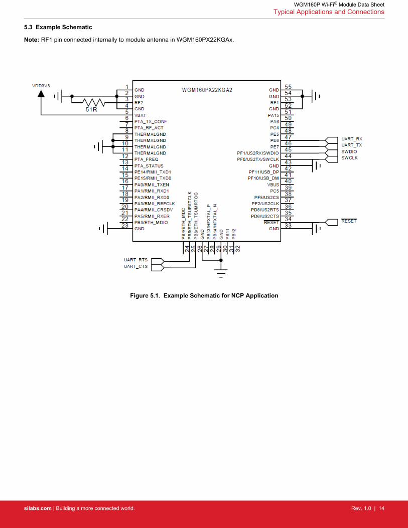
5.3 Example Schematic
Note: RF1 pin connected internally to module antenna in WGM160PX22KGAx.
Figure 5.1. Example Schematic for NCP Application
WGM160P Wi-Fi® Module Data SheetTypical Applications and Connections
silabs.com | Building a more connected world. Rev. 1.0 | 14
6. Gecko OS Features
The Gecko OS software supplied with the WGM160P provides a wide range of features beyond the underlying hardware, and supportsapplication development via its command API.
For complete documentation of Gecko OS, see https://docs.silabs.com/gecko-os/.Software APIs• Gecko OS Command API• Gecko OS Native C API
Interfaces• Serial (UART, remote terminal)• SoftAP and WLAN client (concurrent)• I2C master• SPI master
Servers• TCP/TLS, UDP, HTTP(S), DHCP, DNS• HTTP(S) Server with RESTful API and Websockets
Clients
• TCP/TLS, UDP, NTP, Secure-SMTP, DHCP, DNS• HTTP(S) client• Websocket client
Setup
• Multiple Wi-Fi setup options, including via serial command andWeb setup with SoftAP
Peripherals and Sensors
• GPIOs for control, indication and monitoring• I2C-master API for interfacing to external peripherals• SPI-master API for interfacing to external peripherals• Automated broadcast and streaming of sensor data• Local caching of sensor data
Update and Recovery
• Wireless OTA (Over-the-Air) update to remote manage firm-ware using the Zentri DMS (Device Management Service)
System Management
• System configuration and monitoring via setting and getting awide range of variables
• Configurable power states• Sleep/wake timers
File System
• Read/write file system with appendable log files• Storage of large files• Optional additional bulk serial flash• HTTP download to file system, HTTP upload from file system
WGM160P Wi-Fi® Module Data SheetGecko OS Features
silabs.com | Building a more connected world. Rev. 1.0 | 15
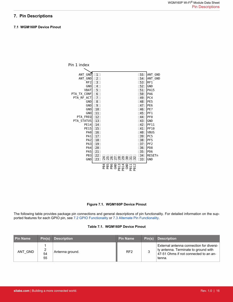
7. Pin Descriptions
7.1 WGM160P Device Pinout
Figure 7.1. WGM160P Device Pinout
The following table provides package pin connections and general descriptions of pin functionality. For detailed information on the sup-ported features for each GPIO pin, see 7.2 GPIO Functionality or 7.3 Alternate Pin Functionality.
Table 7.1. WGM160P Device Pinout
Pin Name Pin(s) Description Pin Name Pin(s) Description
ANT_GND
125455
Antenna ground. RF2 3
External antenna connection for diversi-ty antenna. Terminate to ground with47-51 Ohms if not connected to an an-tenna.
WGM160P Wi-Fi® Module Data SheetPin Descriptions
silabs.com | Building a more connected world. Rev. 1.0 | 16
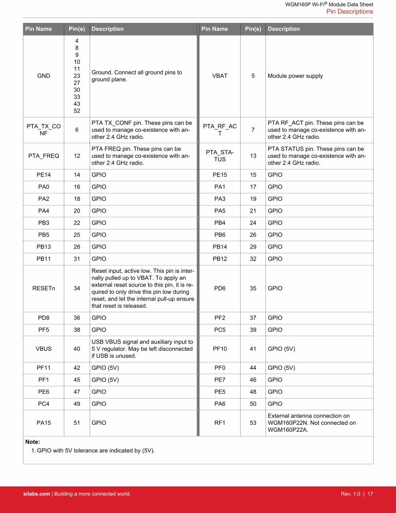
Pin Name Pin(s) Description Pin Name Pin(s) Description
GND
4891011232730334352
Ground. Connect all ground pins toground plane. VBAT 5 Module power supply
PTA_TX_CONF 6
PTA TX_CONF pin. These pins can beused to manage co-existence with an-other 2.4 GHz radio.
PTA_RF_ACT 7
PTA RF_ACT pin. These pins can beused to manage co-existence with an-other 2.4 GHz radio.
PTA_FREQ 12PTA FREQ pin. These pins can beused to manage co-existence with an-other 2.4 GHz radio.
PTA_STA-TUS 13
PTA STATUS pin. These pins can beused to manage co-existence with an-other 2.4 GHz radio.
PE14 14 GPIO PE15 15 GPIO
PA0 16 GPIO PA1 17 GPIO
PA2 18 GPIO PA3 19 GPIO
PA4 20 GPIO PA5 21 GPIO
PB3 22 GPIO PB4 24 GPIO
PB5 25 GPIO PB6 26 GPIO
PB13 28 GPIO PB14 29 GPIO
PB11 31 GPIO PB12 32 GPIO
RESETn 34
Reset input, active low. This pin is inter-nally pulled up to VBAT. To apply anexternal reset source to this pin, it is re-quired to only drive this pin low duringreset, and let the internal pull-up ensurethat reset is released.
PD6 35 GPIO
PD8 36 GPIO PF2 37 GPIO
PF5 38 GPIO PC5 39 GPIO
VBUS 40USB VBUS signal and auxiliary input to5 V regulator. May be left disconnectedif USB is unused.
PF10 41 GPIO (5V)
PF11 42 GPIO (5V) PF0 44 GPIO (5V)
PF1 45 GPIO (5V) PE7 46 GPIO
PE6 47 GPIO PE5 48 GPIO
PC4 49 GPIO PA6 50 GPIO
PA15 51 GPIO RF1 53External antenna connection onWGM160P22N. Not connected onWGM160P22A.
Note:1. GPIO with 5V tolerance are indicated by (5V).
WGM160P Wi-Fi® Module Data SheetPin Descriptions
silabs.com | Building a more connected world. Rev. 1.0 | 17
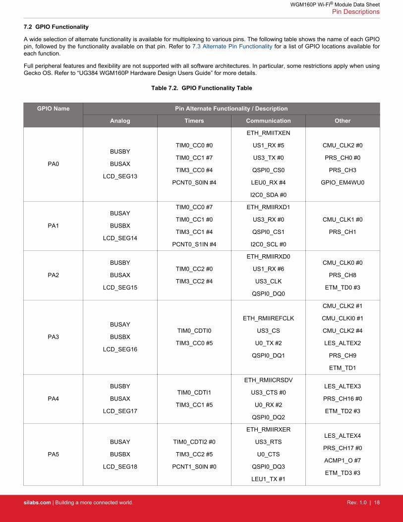
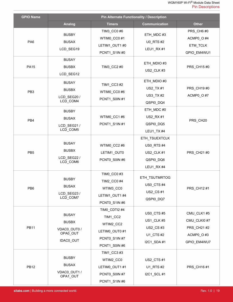
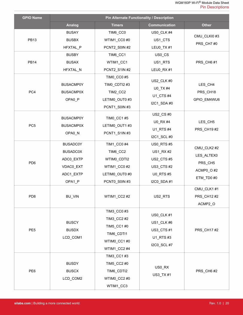
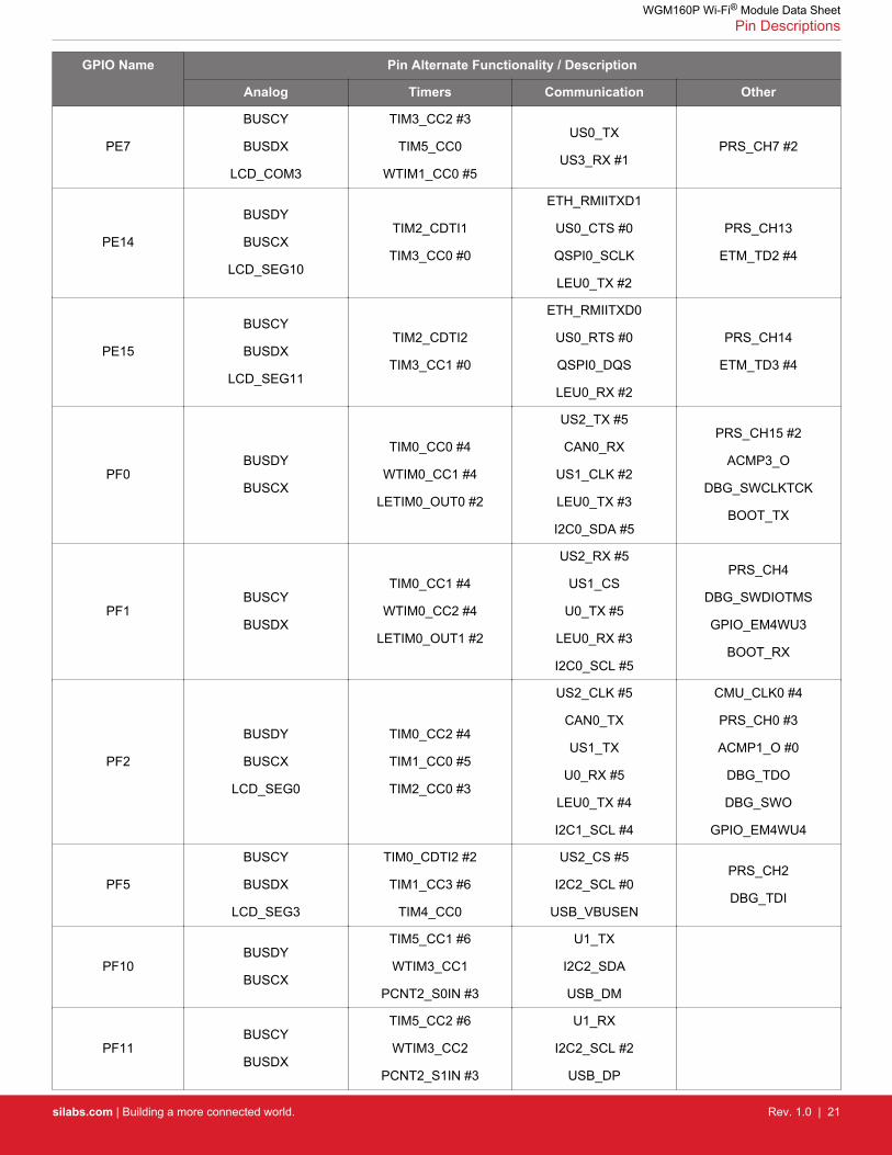
7.2 GPIO Functionality
A wide selection of alternate functionality is available for multiplexing to various pins. The following table shows the name of each GPIOpin, followed by the functionality available on that pin. Refer to 7.3 Alternate Pin Functionality for a list of GPIO locations available foreach function.
Full peripheral features and flexibility are not supported with all software architectures. In particular, some restrictions apply when usingGecko OS. Refer to “UG384 WGM160P Hardware Design Users Guide” for more details.
Table 7.2. GPIO Functionality Table
GPIO Name Pin Alternate Functionality / Description
Analog Timers Communication Other
PA0
BUSBY
BUSAX
LCD_SEG13
TIM0_CC0 #0
TIM0_CC1 #7
TIM3_CC0 #4
PCNT0_S0IN #4
ETH_RMIITXEN
US1_RX #5
US3_TX #0
QSPI0_CS0
LEU0_RX #4
I2C0_SDA #0
CMU_CLK2 #0
PRS_CH0 #0
PRS_CH3
GPIO_EM4WU0
PA1
BUSAY
BUSBX
LCD_SEG14
TIM0_CC0 #7
TIM0_CC1 #0
TIM3_CC1 #4
PCNT0_S1IN #4
ETH_RMIIRXD1
US3_RX #0
QSPI0_CS1
I2C0_SCL #0
CMU_CLK1 #0
PRS_CH1
PA2
BUSBY
BUSAX
LCD_SEG15
TIM0_CC2 #0
TIM3_CC2 #4
ETH_RMIIRXD0
US1_RX #6
US3_CLK
QSPI0_DQ0
CMU_CLK0 #0
PRS_CH8
ETM_TD0 #3
PA3
BUSAY
BUSBX
LCD_SEG16
TIM0_CDTI0
TIM3_CC0 #5
ETH_RMIIREFCLK
US3_CS
U0_TX #2
QSPI0_DQ1
CMU_CLK2 #1
CMU_CLKI0 #1
CMU_CLK2 #4
LES_ALTEX2
PRS_CH9
ETM_TD1
PA4
BUSBY
BUSAX
LCD_SEG17
TIM0_CDTI1
TIM3_CC1 #5
ETH_RMIICRSDV
US3_CTS #0
U0_RX #2
QSPI0_DQ2
LES_ALTEX3
PRS_CH16 #0
ETM_TD2 #3
PA5
BUSAY
BUSBX
LCD_SEG18
TIM0_CDTI2 #0
TIM3_CC2 #5
PCNT1_S0IN #0
ETH_RMIIRXER
US3_RTS
U0_CTS
QSPI0_DQ3
LEU1_TX #1
LES_ALTEX4
PRS_CH17 #0
ACMP1_O #7
ETM_TD3 #3
WGM160P Wi-Fi® Module Data SheetPin Descriptions
silabs.com | Building a more connected world. Rev. 1.0 | 18
GPIO Name Pin Alternate Functionality / Description
Analog Timers Communication Other
PA6
BUSBY
BUSAX
LCD_SEG19
TIM3_CC0 #6
WTIM0_CC0 #1
LETIM1_OUT1 #0
PCNT1_S1IN #0
ETH_MDC #3
U0_RTS #2
LEU1_RX #1
PRS_CH6 #0
ACMP0_O #4
ETM_TCLK
GPIO_EM4WU1
PA15
BUSAY
BUSBX
LCD_SEG12
TIM3_CC2 #0ETH_MDIO #3
US2_CLK #3PRS_CH15 #0
PB3
BUSAY
BUSBX
LCD_SEG20 /LCD_COM4
TIM1_CC3 #2
WTIM0_CC0 #6
PCNT1_S0IN #1
ETH_MDIO #0
US2_TX #1
US3_TX #2
QSPI0_DQ4
PRS_CH19 #0
ACMP0_O #7
PB4
BUSBY
BUSAX
LCD_SEG21 /LCD_COM5
WTIM0_CC1 #6
PCNT1_S1IN #1
ETH_MDC #0
US2_RX #1
QSPI0_DQ5
LEU1_TX #4
PRS_CH20
PB5
BUSAY
BUSBX
LCD_SEG22 /LCD_COM6
WTIM0_CC2 #6
LETIM1_OUT0
PCNT0_S0IN #6
ETH_TSUEXTCLK
US0_RTS #4
US2_CLK #1
QSPI0_DQ6
LEU1_RX #4
PRS_CH21 #0
PB6
BUSBY
BUSAX
LCD_SEG23 /LCD_COM7
TIM0_CC0 #3
TIM2_CC0 #4
WTIM3_CC0
LETIM1_OUT1 #4
PCNT0_S1IN #6
ETH_TSUTMRTOG
US0_CTS #4
US2_CS #1
QSPI0_DQ7
PRS_CH12 #1
PB11
BUSAY
BUSBX
VDAC0_OUT0 /OPA0_OUT
IDAC0_OUT
TIM0_CDTI2 #4
TIM1_CC2
WTIM2_CC2
LETIM0_OUT0 #1
PCNT0_S1IN #7
PCNT1_S0IN #6
US0_CTS #5
US1_CLK #5
US2_CS #3
U1_CTS #2
I2C1_SDA #1
CMU_CLK1 #5
CMU_CLKI0 #7
PRS_CH21 #2
ACMP0_O #3
GPIO_EM4WU7
PB12
BUSBY
BUSAX
VDAC0_OUT1 /OPA1_OUT
TIM1_CC3 #3
WTIM2_CC0
LETIM0_OUT1 #1
PCNT0_S0IN #7
PCNT1_S1IN #6
US2_CTS #1
U1_RTS #2
I2C1_SCL #1
PRS_CH16 #1
WGM160P Wi-Fi® Module Data SheetPin Descriptions
silabs.com | Building a more connected world. Rev. 1.0 | 19
GPIO Name Pin Alternate Functionality / Description
Analog Timers Communication Other
PB13
BUSAY
BUSBX
HFXTAL_P
TIM6_CC0
WTIM1_CC0 #0
PCNT2_S0IN #2
US0_CLK #4
US1_CTS
LEU0_TX #1
CMU_CLKI0 #3
PRS_CH7 #0
PB14
BUSBY
BUSAX
HFXTAL_N
TIM6_CC1
WTIM1_CC1
PCNT2_S1IN #2
US0_CS
US1_RTS
LEU0_RX #1
PRS_CH6 #1
PC4
BUSACMP0Y
BUSACMP0X
OPA0_P
TIM0_CC0 #5
TIM0_CDTI2 #3
TIM2_CC2
LETIM0_OUT0 #3
PCNT1_S0IN #3
US2_CLK #0
U0_TX #4
U1_CTS #4
I2C1_SDA #0
LES_CH4
PRS_CH18
GPIO_EM4WU6
PC5
BUSACMP0Y
BUSACMP0X
OPA0_N
TIM0_CC1 #5
LETIM0_OUT1 #3
PCNT1_S1IN #3
US2_CS #0
U0_RX #4
U1_RTS #4
I2C1_SCL #0
LES_CH5
PRS_CH19 #2
PD6
BUSADC0Y
BUSADC0X
ADC0_EXTP
VDAC0_EXT
ADC1_EXTP
OPA1_P
TIM1_CC0 #4
TIM6_CC2
WTIM0_CDTI2
WTIM1_CC0 #2
LETIM0_OUT0 #0
PCNT0_S0IN #3
US0_RTS #5
US1_RX #2
US2_CTS #5
US3_CTS #2
U0_RTS #5
I2C0_SDA #1
CMU_CLK2 #2
LES_ALTEX0
PRS_CH5
ACMP0_O #2
ETM_TD0 #0
PD8 BU_VIN WTIM1_CC2 #2 US2_RTS
CMU_CLK1 #1
PRS_CH12 #2
ACMP2_O
PE5
BUSCY
BUSDX
LCD_COM1
TIM3_CC0 #3
TIM3_CC2 #2
TIM5_CC1 #0
TIM6_CDTI1
WTIM0_CC1 #0
WTIM1_CC2 #4
US0_CLK #1
US1_CLK #6
US3_CTS #1
U1_RTS #3
I2C0_SCL #7
PRS_CH17 #2
PE6
BUSDY
BUSCX
LCD_COM2
TIM3_CC1 #3
TIM5_CC2 #0
TIM6_CDTI2
WTIM0_CC2 #0
WTIM1_CC3
US0_RX
US3_TX #1PRS_CH6 #2
WGM160P Wi-Fi® Module Data SheetPin Descriptions
silabs.com | Building a more connected world. Rev. 1.0 | 20
GPIO Name Pin Alternate Functionality / Description
Analog Timers Communication Other
PE7
BUSCY
BUSDX
LCD_COM3
TIM3_CC2 #3
TIM5_CC0
WTIM1_CC0 #5
US0_TX
US3_RX #1PRS_CH7 #2
PE14
BUSDY
BUSCX
LCD_SEG10
TIM2_CDTI1
TIM3_CC0 #0
ETH_RMIITXD1
US0_CTS #0
QSPI0_SCLK
LEU0_TX #2
PRS_CH13
ETM_TD2 #4
PE15
BUSCY
BUSDX
LCD_SEG11
TIM2_CDTI2
TIM3_CC1 #0
ETH_RMIITXD0
US0_RTS #0
QSPI0_DQS
LEU0_RX #2
PRS_CH14
ETM_TD3 #4
PF0BUSDY
BUSCX
TIM0_CC0 #4
WTIM0_CC1 #4
LETIM0_OUT0 #2
US2_TX #5
CAN0_RX
US1_CLK #2
LEU0_TX #3
I2C0_SDA #5
PRS_CH15 #2
ACMP3_O
DBG_SWCLKTCK
BOOT_TX
PF1BUSCY
BUSDX
TIM0_CC1 #4
WTIM0_CC2 #4
LETIM0_OUT1 #2
US2_RX #5
US1_CS
U0_TX #5
LEU0_RX #3
I2C0_SCL #5
PRS_CH4
DBG_SWDIOTMS
GPIO_EM4WU3
BOOT_RX
PF2
BUSDY
BUSCX
LCD_SEG0
TIM0_CC2 #4
TIM1_CC0 #5
TIM2_CC0 #3
US2_CLK #5
CAN0_TX
US1_TX
U0_RX #5
LEU0_TX #4
I2C1_SCL #4
CMU_CLK0 #4
PRS_CH0 #3
ACMP1_O #0
DBG_TDO
DBG_SWO
GPIO_EM4WU4
PF5
BUSCY
BUSDX
LCD_SEG3
TIM0_CDTI2 #2
TIM1_CC3 #6
TIM4_CC0
US2_CS #5
I2C2_SCL #0
USB_VBUSEN
PRS_CH2
DBG_TDI
PF10BUSDY
BUSCX
TIM5_CC1 #6
WTIM3_CC1
PCNT2_S0IN #3
U1_TX
I2C2_SDA
USB_DM
PF11BUSCY
BUSDX
TIM5_CC2 #6
WTIM3_CC2
PCNT2_S1IN #3
U1_RX
I2C2_SCL #2
USB_DP
WGM160P Wi-Fi® Module Data SheetPin Descriptions
silabs.com | Building a more connected world. Rev. 1.0 | 21
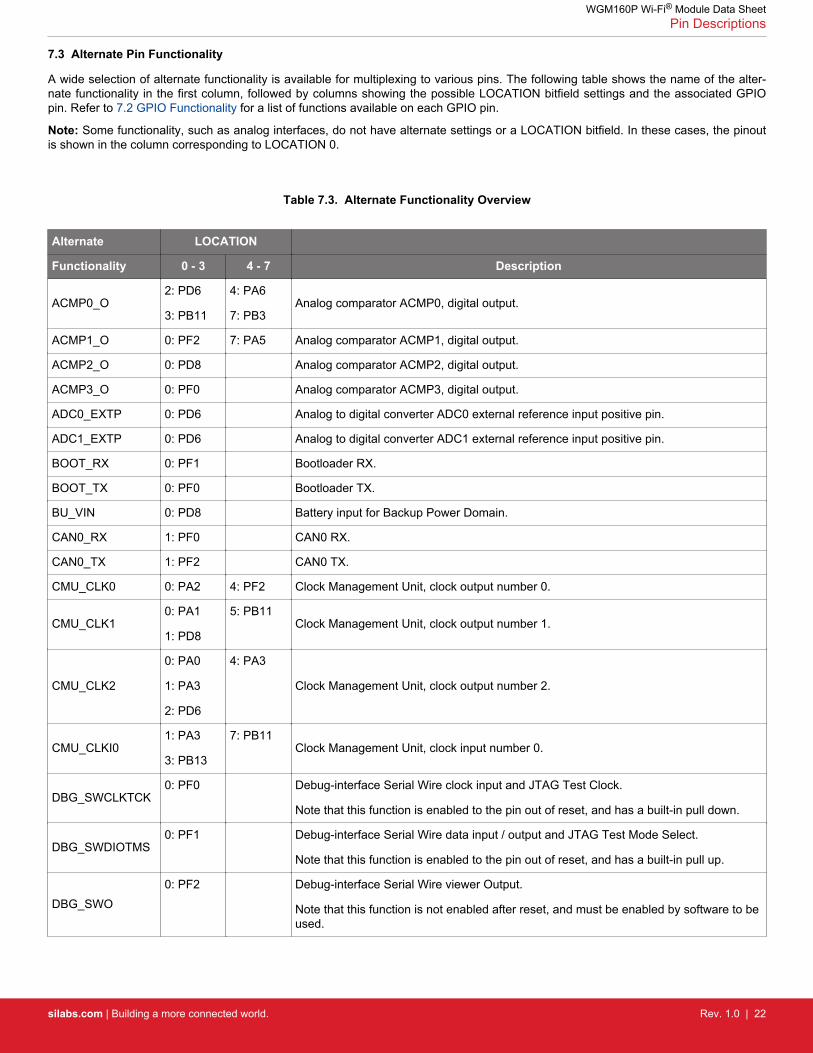
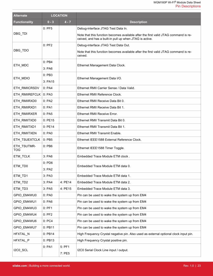
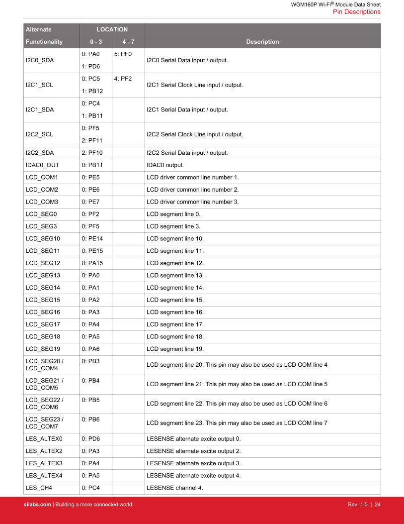
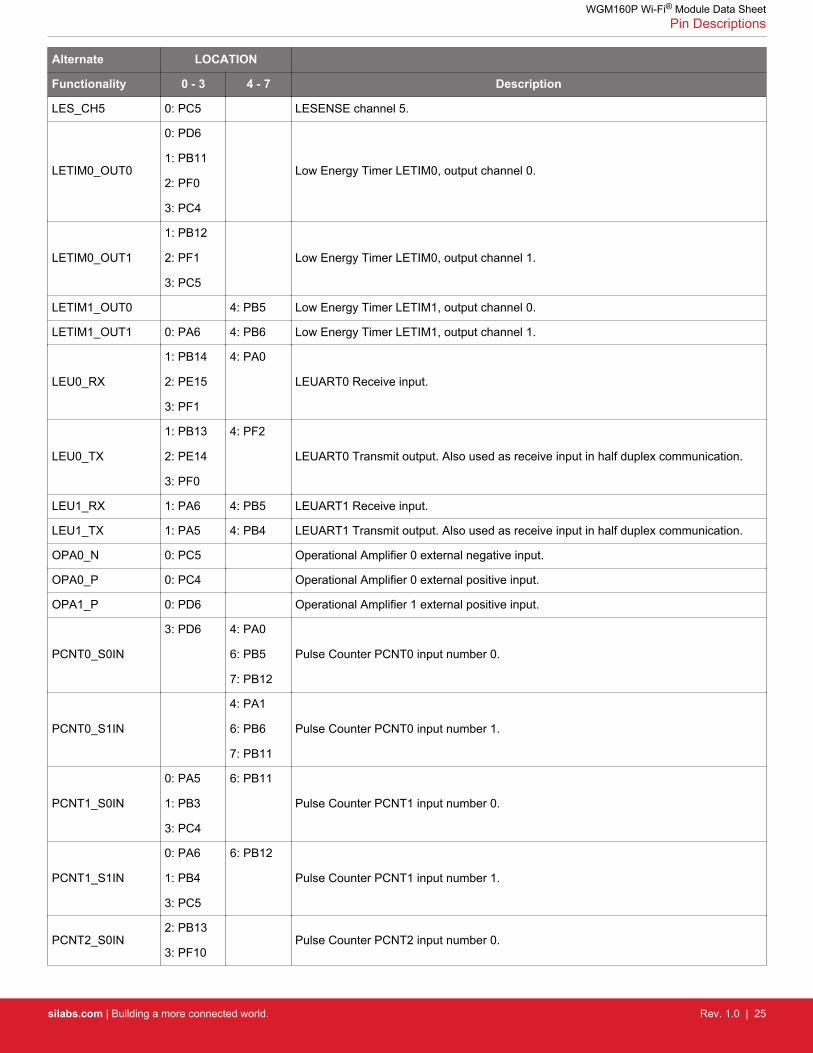
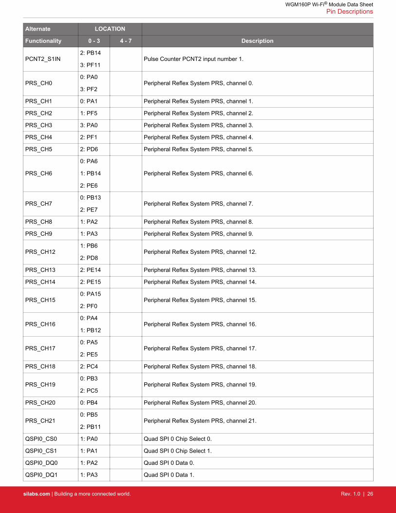
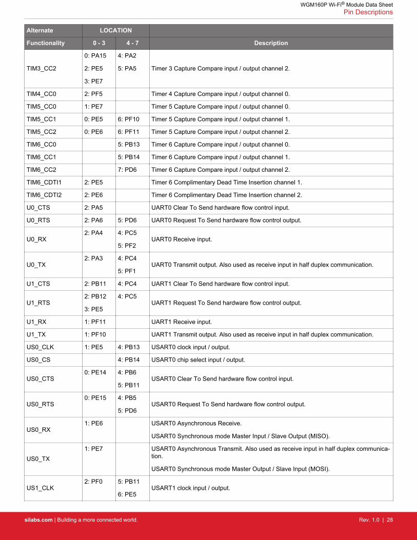
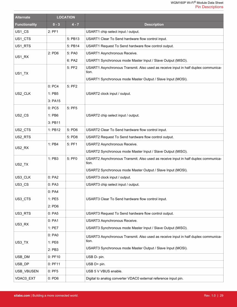
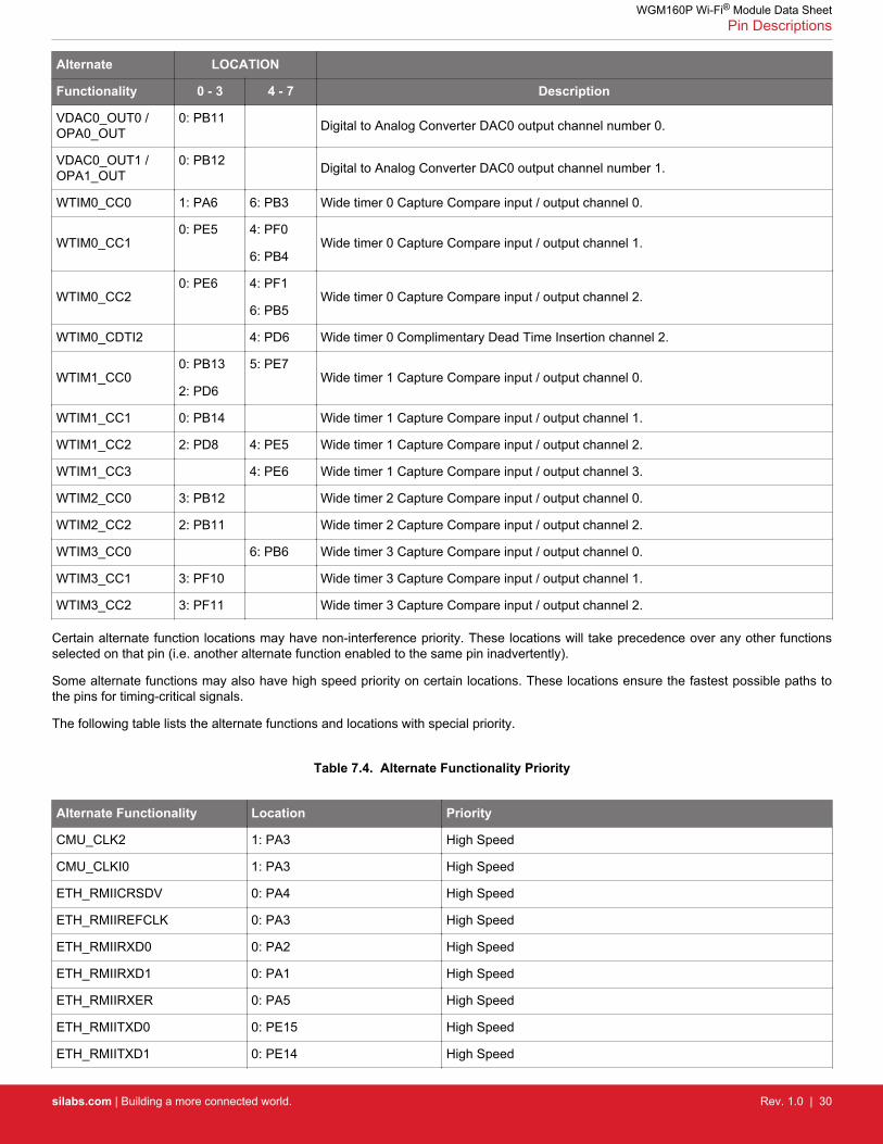
7.3 Alternate Pin Functionality
A wide selection of alternate functionality is available for multiplexing to various pins. The following table shows the name of the alter-nate functionality in the first column, followed by columns showing the possible LOCATION bitfield settings and the associated GPIOpin. Refer to 7.2 GPIO Functionality for a list of functions available on each GPIO pin.
Note: Some functionality, such as analog interfaces, do not have alternate settings or a LOCATION bitfield. In these cases, the pinoutis shown in the column corresponding to LOCATION 0.
Table 7.3. Alternate Functionality Overview
Alternate LOCATION
Functionality 0 - 3 4 - 7 Description
ACMP0_O2: PD6
3: PB11
4: PA6
7: PB3Analog comparator ACMP0, digital output.
ACMP1_O 0: PF2 7: PA5 Analog comparator ACMP1, digital output.
ACMP2_O 0: PD8 Analog comparator ACMP2, digital output.
ACMP3_O 0: PF0 Analog comparator ACMP3, digital output.
ADC0_EXTP 0: PD6 Analog to digital converter ADC0 external reference input positive pin.
ADC1_EXTP 0: PD6 Analog to digital converter ADC1 external reference input positive pin.
BOOT_RX 0: PF1 Bootloader RX.
BOOT_TX 0: PF0 Bootloader TX.
BU_VIN 0: PD8 Battery input for Backup Power Domain.
CAN0_RX 1: PF0 CAN0 RX.
CAN0_TX 1: PF2 CAN0 TX.
CMU_CLK0 0: PA2 4: PF2 Clock Management Unit, clock output number 0.
CMU_CLK10: PA1
1: PD8
5: PB11Clock Management Unit, clock output number 1.
CMU_CLK2
0: PA0
1: PA3
2: PD6
4: PA3
Clock Management Unit, clock output number 2.
CMU_CLKI01: PA3
3: PB13
7: PB11Clock Management Unit, clock input number 0.
DBG_SWCLKTCK0: PF0 Debug-interface Serial Wire clock input and JTAG Test Clock.
Note that this function is enabled to the pin out of reset, and has a built-in pull down.
DBG_SWDIOTMS0: PF1 Debug-interface Serial Wire data input / output and JTAG Test Mode Select.
Note that this function is enabled to the pin out of reset, and has a built-in pull up.
DBG_SWO0: PF2 Debug-interface Serial Wire viewer Output.
Note that this function is not enabled after reset, and must be enabled by software to beused.
WGM160P Wi-Fi® Module Data SheetPin Descriptions
silabs.com | Building a more connected world. Rev. 1.0 | 22
Alternate LOCATION
Functionality 0 - 3 4 - 7 Description
DBG_TDI0: PF5 Debug-interface JTAG Test Data In.
Note that this function becomes available after the first valid JTAG command is re-ceived, and has a built-in pull up when JTAG is active.
DBG_TDO0: PF2 Debug-interface JTAG Test Data Out.
Note that this function becomes available after the first valid JTAG command is re-ceived.
ETH_MDC0: PB4
3: PA6Ethernet Management Data Clock.
ETH_MDIO0: PB3
3: PA15Ethernet Management Data I/O.
ETH_RMIICRSDV 0: PA4 Ethernet RMII Carrier Sense / Data Valid.
ETH_RMIIREFCLK 0: PA3 Ethernet RMII Reference Clock.
ETH_RMIIRXD0 0: PA2 Ethernet RMII Receive Data Bit 0.
ETH_RMIIRXD1 0: PA1 Ethernet RMII Receive Data Bit 1.
ETH_RMIIRXER 0: PA5 Ethernet RMII Receive Error.
ETH_RMIITXD0 0: PE15 Ethernet RMII Transmit Data Bit 0.
ETH_RMIITXD1 0: PE14 Ethernet RMII Transmit Data Bit 1.
ETH_RMIITXEN 0: PA0 Ethernet RMII Transmit Enable.
ETH_TSUEXTCLK 0: PB5 Ethernet IEEE1588 External Reference Clock.
ETH_TSUTMR-TOG
0: PB6 Ethernet IEEE1588 Timer Toggle.
ETM_TCLK 3: PA6 Embedded Trace Module ETM clock .
ETM_TD00: PD6
3: PA2Embedded Trace Module ETM data 0.
ETM_TD1 3: PA3 Embedded Trace Module ETM data 1.
ETM_TD2 3: PA4 4: PE14 Embedded Trace Module ETM data 2.
ETM_TD3 3: PA5 4: PE15 Embedded Trace Module ETM data 3.
GPIO_EM4WU0 0: PA0 Pin can be used to wake the system up from EM4
GPIO_EM4WU1 0: PA6 Pin can be used to wake the system up from EM4
GPIO_EM4WU3 0: PF1 Pin can be used to wake the system up from EM4
GPIO_EM4WU4 0: PF2 Pin can be used to wake the system up from EM4
GPIO_EM4WU6 0: PC4 Pin can be used to wake the system up from EM4
GPIO_EM4WU7 0: PB11 Pin can be used to wake the system up from EM4
HFXTAL_N 0: PB14 High Frequency Crystal negative pin. Also used as external optional clock input pin.
HFXTAL_P 0: PB13 High Frequency Crystal positive pin.
I2C0_SCL0: PA1 5: PF1
7: PE5I2C0 Serial Clock Line input / output.
WGM160P Wi-Fi® Module Data SheetPin Descriptions
silabs.com | Building a more connected world. Rev. 1.0 | 23
Alternate LOCATION
Functionality 0 - 3 4 - 7 Description
I2C0_SDA0: PA0
1: PD6
5: PF0I2C0 Serial Data input / output.
I2C1_SCL0: PC5
1: PB12
4: PF2I2C1 Serial Clock Line input / output.
I2C1_SDA0: PC4
1: PB11I2C1 Serial Data input / output.
I2C2_SCL0: PF5
2: PF11I2C2 Serial Clock Line input / output.
I2C2_SDA 2: PF10 I2C2 Serial Data input / output.
IDAC0_OUT 0: PB11 IDAC0 output.
LCD_COM1 0: PE5 LCD driver common line number 1.
LCD_COM2 0: PE6 LCD driver common line number 2.
LCD_COM3 0: PE7 LCD driver common line number 3.
LCD_SEG0 0: PF2 LCD segment line 0.
LCD_SEG3 0: PF5 LCD segment line 3.
LCD_SEG10 0: PE14 LCD segment line 10.
LCD_SEG11 0: PE15 LCD segment line 11.
LCD_SEG12 0: PA15 LCD segment line 12.
LCD_SEG13 0: PA0 LCD segment line 13.
LCD_SEG14 0: PA1 LCD segment line 14.
LCD_SEG15 0: PA2 LCD segment line 15.
LCD_SEG16 0: PA3 LCD segment line 16.
LCD_SEG17 0: PA4 LCD segment line 17.
LCD_SEG18 0: PA5 LCD segment line 18.
LCD_SEG19 0: PA6 LCD segment line 19.
LCD_SEG20 /LCD_COM4
0: PB3 LCD segment line 20. This pin may also be used as LCD COM line 4
LCD_SEG21 /LCD_COM5
0: PB4 LCD segment line 21. This pin may also be used as LCD COM line 5
LCD_SEG22 /LCD_COM6
0: PB5 LCD segment line 22. This pin may also be used as LCD COM line 6
LCD_SEG23 /LCD_COM7
0: PB6 LCD segment line 23. This pin may also be used as LCD COM line 7
LES_ALTEX0 0: PD6 LESENSE alternate excite output 0.
LES_ALTEX2 0: PA3 LESENSE alternate excite output 2.
LES_ALTEX3 0: PA4 LESENSE alternate excite output 3.
LES_ALTEX4 0: PA5 LESENSE alternate excite output 4.
LES_CH4 0: PC4 LESENSE channel 4.
WGM160P Wi-Fi® Module Data SheetPin Descriptions
silabs.com | Building a more connected world. Rev. 1.0 | 24
Alternate LOCATION
Functionality 0 - 3 4 - 7 Description
LES_CH5 0: PC5 LESENSE channel 5.
LETIM0_OUT0
0: PD6
1: PB11
2: PF0
3: PC4
Low Energy Timer LETIM0, output channel 0.
LETIM0_OUT1
1: PB12
2: PF1
3: PC5
Low Energy Timer LETIM0, output channel 1.
LETIM1_OUT0 4: PB5 Low Energy Timer LETIM1, output channel 0.
LETIM1_OUT1 0: PA6 4: PB6 Low Energy Timer LETIM1, output channel 1.
LEU0_RX
1: PB14
2: PE15
3: PF1
4: PA0
LEUART0 Receive input.
LEU0_TX
1: PB13
2: PE14
3: PF0
4: PF2
LEUART0 Transmit output. Also used as receive input in half duplex communication.
LEU1_RX 1: PA6 4: PB5 LEUART1 Receive input.
LEU1_TX 1: PA5 4: PB4 LEUART1 Transmit output. Also used as receive input in half duplex communication.
OPA0_N 0: PC5 Operational Amplifier 0 external negative input.
OPA0_P 0: PC4 Operational Amplifier 0 external positive input.
OPA1_P 0: PD6 Operational Amplifier 1 external positive input.
PCNT0_S0IN
3: PD6 4: PA0
6: PB5
7: PB12
Pulse Counter PCNT0 input number 0.
PCNT0_S1IN
4: PA1
6: PB6
7: PB11
Pulse Counter PCNT0 input number 1.
PCNT1_S0IN
0: PA5
1: PB3
3: PC4
6: PB11
Pulse Counter PCNT1 input number 0.
PCNT1_S1IN
0: PA6
1: PB4
3: PC5
6: PB12
Pulse Counter PCNT1 input number 1.
PCNT2_S0IN2: PB13
3: PF10Pulse Counter PCNT2 input number 0.
WGM160P Wi-Fi® Module Data SheetPin Descriptions
silabs.com | Building a more connected world. Rev. 1.0 | 25
Alternate LOCATION
Functionality 0 - 3 4 - 7 Description
PCNT2_S1IN2: PB14
3: PF11Pulse Counter PCNT2 input number 1.
PRS_CH00: PA0
3: PF2Peripheral Reflex System PRS, channel 0.
PRS_CH1 0: PA1 Peripheral Reflex System PRS, channel 1.
PRS_CH2 1: PF5 Peripheral Reflex System PRS, channel 2.
PRS_CH3 3: PA0 Peripheral Reflex System PRS, channel 3.
PRS_CH4 2: PF1 Peripheral Reflex System PRS, channel 4.
PRS_CH5 2: PD6 Peripheral Reflex System PRS, channel 5.
PRS_CH6
0: PA6
1: PB14
2: PE6
Peripheral Reflex System PRS, channel 6.
PRS_CH70: PB13
2: PE7Peripheral Reflex System PRS, channel 7.
PRS_CH8 1: PA2 Peripheral Reflex System PRS, channel 8.
PRS_CH9 1: PA3 Peripheral Reflex System PRS, channel 9.
PRS_CH121: PB6
2: PD8Peripheral Reflex System PRS, channel 12.
PRS_CH13 2: PE14 Peripheral Reflex System PRS, channel 13.
PRS_CH14 2: PE15 Peripheral Reflex System PRS, channel 14.
PRS_CH150: PA15
2: PF0Peripheral Reflex System PRS, channel 15.
PRS_CH160: PA4
1: PB12Peripheral Reflex System PRS, channel 16.
PRS_CH170: PA5
2: PE5Peripheral Reflex System PRS, channel 17.
PRS_CH18 2: PC4 Peripheral Reflex System PRS, channel 18.
PRS_CH190: PB3
2: PC5Peripheral Reflex System PRS, channel 19.
PRS_CH20 0: PB4 Peripheral Reflex System PRS, channel 20.
PRS_CH210: PB5
2: PB11Peripheral Reflex System PRS, channel 21.
QSPI0_CS0 1: PA0 Quad SPI 0 Chip Select 0.
QSPI0_CS1 1: PA1 Quad SPI 0 Chip Select 1.
QSPI0_DQ0 1: PA2 Quad SPI 0 Data 0.
QSPI0_DQ1 1: PA3 Quad SPI 0 Data 1.
WGM160P Wi-Fi® Module Data SheetPin Descriptions
silabs.com | Building a more connected world. Rev. 1.0 | 26

Alternate LOCATION
Functionality 0 - 3 4 - 7 Description
QSPI0_DQ2 1: PA4 Quad SPI 0 Data 2.
QSPI0_DQ3 1: PA5 Quad SPI 0 Data 3.
QSPI0_DQ4 1: PB3 Quad SPI 0 Data 4.
QSPI0_DQ5 1: PB4 Quad SPI 0 Data 5.
QSPI0_DQ6 1: PB5 Quad SPI 0 Data 6.
QSPI0_DQ7 1: PB6 Quad SPI 0 Data 7.
QSPI0_DQS 1: PE15 Quad SPI 0 Data S.
QSPI0_SCLK 1: PE14 Quad SPI 0 Serial Clock.
TIM0_CC0
0: PA0
3: PB6
4: PF0
5: PC4
7: PA1
Timer 0 Capture Compare input / output channel 0.
TIM0_CC1
0: PA1 4: PF1
5: PC5
7: PA0
Timer 0 Capture Compare input / output channel 1.
TIM0_CC2 0: PA2 4: PF2 Timer 0 Capture Compare input / output channel 2.
TIM0_CDTI0 0: PA3 Timer 0 Complimentary Dead Time Insertion channel 0.
TIM0_CDTI1 0: PA4 Timer 0 Complimentary Dead Time Insertion channel 1.
TIM0_CDTI2
0: PA5
2: PF5
3: PC4
4: PB11
Timer 0 Complimentary Dead Time Insertion channel 2.
TIM1_CC04: PD6
5: PF2Timer 1 Capture Compare input / output channel 0.
TIM1_CC2 3: PB11 Timer 1 Capture Compare input / output channel 2.
TIM1_CC32: PB3
3: PB12
6: PF5Timer 1 Capture Compare input / output channel 3.
TIM2_CC0 3: PF2 4: PB6 Timer 2 Capture Compare input / output channel 0.
TIM2_CC2 5: PC4 Timer 2 Capture Compare input / output channel 2.
TIM2_CDTI1 2: PE14 Timer 2 Complimentary Dead Time Insertion channel 1.
TIM2_CDTI2 2: PE15 Timer 2 Complimentary Dead Time Insertion channel 2.
TIM3_CC0
0: PE14
3: PE5
4: PA0
5: PA3
6: PA6
Timer 3 Capture Compare input / output channel 0.
TIM3_CC10: PE15
3: PE6
4: PA1
5: PA4Timer 3 Capture Compare input / output channel 1.
WGM160P Wi-Fi® Module Data SheetPin Descriptions
silabs.com | Building a more connected world. Rev. 1.0 | 27
Alternate LOCATION
Functionality 0 - 3 4 - 7 Description
TIM3_CC2
0: PA15
2: PE5
3: PE7
4: PA2
5: PA5 Timer 3 Capture Compare input / output channel 2.
TIM4_CC0 2: PF5 Timer 4 Capture Compare input / output channel 0.
TIM5_CC0 1: PE7 Timer 5 Capture Compare input / output channel 0.
TIM5_CC1 0: PE5 6: PF10 Timer 5 Capture Compare input / output channel 1.
TIM5_CC2 0: PE6 6: PF11 Timer 5 Capture Compare input / output channel 2.
TIM6_CC0 5: PB13 Timer 6 Capture Compare input / output channel 0.
TIM6_CC1 5: PB14 Timer 6 Capture Compare input / output channel 1.
TIM6_CC2 7: PD6 Timer 6 Capture Compare input / output channel 2.
TIM6_CDTI1 2: PE5 Timer 6 Complimentary Dead Time Insertion channel 1.
TIM6_CDTI2 2: PE6 Timer 6 Complimentary Dead Time Insertion channel 2.
U0_CTS 2: PA5 UART0 Clear To Send hardware flow control input.
U0_RTS 2: PA6 5: PD6 UART0 Request To Send hardware flow control output.
U0_RX2: PA4 4: PC5
5: PF2UART0 Receive input.
U0_TX2: PA3 4: PC4
5: PF1UART0 Transmit output. Also used as receive input in half duplex communication.
U1_CTS 2: PB11 4: PC4 UART1 Clear To Send hardware flow control input.
U1_RTS2: PB12
3: PE5
4: PC5UART1 Request To Send hardware flow control output.
U1_RX 1: PF11 UART1 Receive input.
U1_TX 1: PF10 UART1 Transmit output. Also used as receive input in half duplex communication.
US0_CLK 1: PE5 4: PB13 USART0 clock input / output.
US0_CS 4: PB14 USART0 chip select input / output.
US0_CTS0: PE14 4: PB6
5: PB11USART0 Clear To Send hardware flow control input.
US0_RTS0: PE15 4: PB5
5: PD6USART0 Request To Send hardware flow control output.
US0_RX1: PE6 USART0 Asynchronous Receive.
USART0 Synchronous mode Master Input / Slave Output (MISO).
US0_TX1: PE7 USART0 Asynchronous Transmit. Also used as receive input in half duplex communica-
tion.
USART0 Synchronous mode Master Output / Slave Input (MOSI).
US1_CLK2: PF0 5: PB11
6: PE5USART1 clock input / output.
WGM160P Wi-Fi® Module Data SheetPin Descriptions
silabs.com | Building a more connected world. Rev. 1.0 | 28
Alternate LOCATION
Functionality 0 - 3 4 - 7 Description
US1_CS 2: PF1 USART1 chip select input / output.
US1_CTS 5: PB13 USART1 Clear To Send hardware flow control input.
US1_RTS 5: PB14 USART1 Request To Send hardware flow control output.
US1_RX2: PD6 5: PA0
6: PA2
USART1 Asynchronous Receive.
USART1 Synchronous mode Master Input / Slave Output (MISO).
US1_TX5: PF2 USART1 Asynchronous Transmit. Also used as receive input in half duplex communica-
tion.
USART1 Synchronous mode Master Output / Slave Input (MOSI).
US2_CLK
0: PC4
1: PB5
3: PA15
5: PF2
USART2 clock input / output.
US2_CS
0: PC5
1: PB6
3: PB11
5: PF5
USART2 chip select input / output.
US2_CTS 1: PB12 5: PD6 USART2 Clear To Send hardware flow control input.
US2_RTS 5: PD8 USART2 Request To Send hardware flow control output.
US2_RX1: PB4 5: PF1 USART2 Asynchronous Receive.
USART2 Synchronous mode Master Input / Slave Output (MISO).
US2_TX1: PB3 5: PF0 USART2 Asynchronous Transmit. Also used as receive input in half duplex communica-
tion.
USART2 Synchronous mode Master Output / Slave Input (MOSI).
US3_CLK 0: PA2 USART3 clock input / output.
US3_CS 0: PA3 USART3 chip select input / output.
US3_CTS
0: PA4
1: PE5
2: PD6
USART3 Clear To Send hardware flow control input.
US3_RTS 0: PA5 USART3 Request To Send hardware flow control output.
US3_RX0: PA1
1: PE7
USART3 Asynchronous Receive.
USART3 Synchronous mode Master Input / Slave Output (MISO).
US3_TX
0: PA0
1: PE6
2: PB3
USART3 Asynchronous Transmit. Also used as receive input in half duplex communica-tion.
USART3 Synchronous mode Master Output / Slave Input (MOSI).
USB_DM 0: PF10 USB D- pin.
USB_DP 0: PF11 USB D+ pin.
USB_VBUSEN 0: PF5 USB 5 V VBUS enable.
VDAC0_EXT 0: PD6 Digital to analog converter VDAC0 external reference input pin.
WGM160P Wi-Fi® Module Data SheetPin Descriptions
silabs.com | Building a more connected world. Rev. 1.0 | 29
Alternate LOCATION
Functionality 0 - 3 4 - 7 Description
VDAC0_OUT0 /OPA0_OUT
0: PB11 Digital to Analog Converter DAC0 output channel number 0.
VDAC0_OUT1 /OPA1_OUT
0: PB12 Digital to Analog Converter DAC0 output channel number 1.
WTIM0_CC0 1: PA6 6: PB3 Wide timer 0 Capture Compare input / output channel 0.
WTIM0_CC10: PE5 4: PF0
6: PB4Wide timer 0 Capture Compare input / output channel 1.
WTIM0_CC20: PE6 4: PF1
6: PB5Wide timer 0 Capture Compare input / output channel 2.
WTIM0_CDTI2 4: PD6 Wide timer 0 Complimentary Dead Time Insertion channel 2.
WTIM1_CC00: PB13
2: PD6
5: PE7Wide timer 1 Capture Compare input / output channel 0.
WTIM1_CC1 0: PB14 Wide timer 1 Capture Compare input / output channel 1.
WTIM1_CC2 2: PD8 4: PE5 Wide timer 1 Capture Compare input / output channel 2.
WTIM1_CC3 4: PE6 Wide timer 1 Capture Compare input / output channel 3.
WTIM2_CC0 3: PB12 Wide timer 2 Capture Compare input / output channel 0.
WTIM2_CC2 2: PB11 Wide timer 2 Capture Compare input / output channel 2.
WTIM3_CC0 6: PB6 Wide timer 3 Capture Compare input / output channel 0.
WTIM3_CC1 3: PF10 Wide timer 3 Capture Compare input / output channel 1.
WTIM3_CC2 3: PF11 Wide timer 3 Capture Compare input / output channel 2.
Certain alternate function locations may have non-interference priority. These locations will take precedence over any other functionsselected on that pin (i.e. another alternate function enabled to the same pin inadvertently).
Some alternate functions may also have high speed priority on certain locations. These locations ensure the fastest possible paths tothe pins for timing-critical signals.
The following table lists the alternate functions and locations with special priority.
Table 7.4. Alternate Functionality Priority
Alternate Functionality Location Priority
CMU_CLK2 1: PA3 High Speed
CMU_CLKI0 1: PA3 High Speed
ETH_RMIICRSDV 0: PA4 High Speed
ETH_RMIIREFCLK 0: PA3 High Speed
ETH_RMIIRXD0 0: PA2 High Speed
ETH_RMIIRXD1 0: PA1 High Speed
ETH_RMIIRXER 0: PA5 High Speed
ETH_RMIITXD0 0: PE15 High Speed
ETH_RMIITXD1 0: PE14 High Speed
WGM160P Wi-Fi® Module Data SheetPin Descriptions
silabs.com | Building a more connected world. Rev. 1.0 | 30

Alternate Functionality Location Priority
ETH_RMIITXEN 0: PA0 High Speed
TIM0_CC0 3: PB6 Non-interference
US2_CLK 5: PF2 High Speed
US2_CS 5: PF5 High Speed
US2_RX 5: PF1 High Speed
US2_TX 5: PF0 High Speed
WGM160P Wi-Fi® Module Data SheetPin Descriptions
silabs.com | Building a more connected world. Rev. 1.0 | 31
8. Package Specifications
8.1 Package Outline
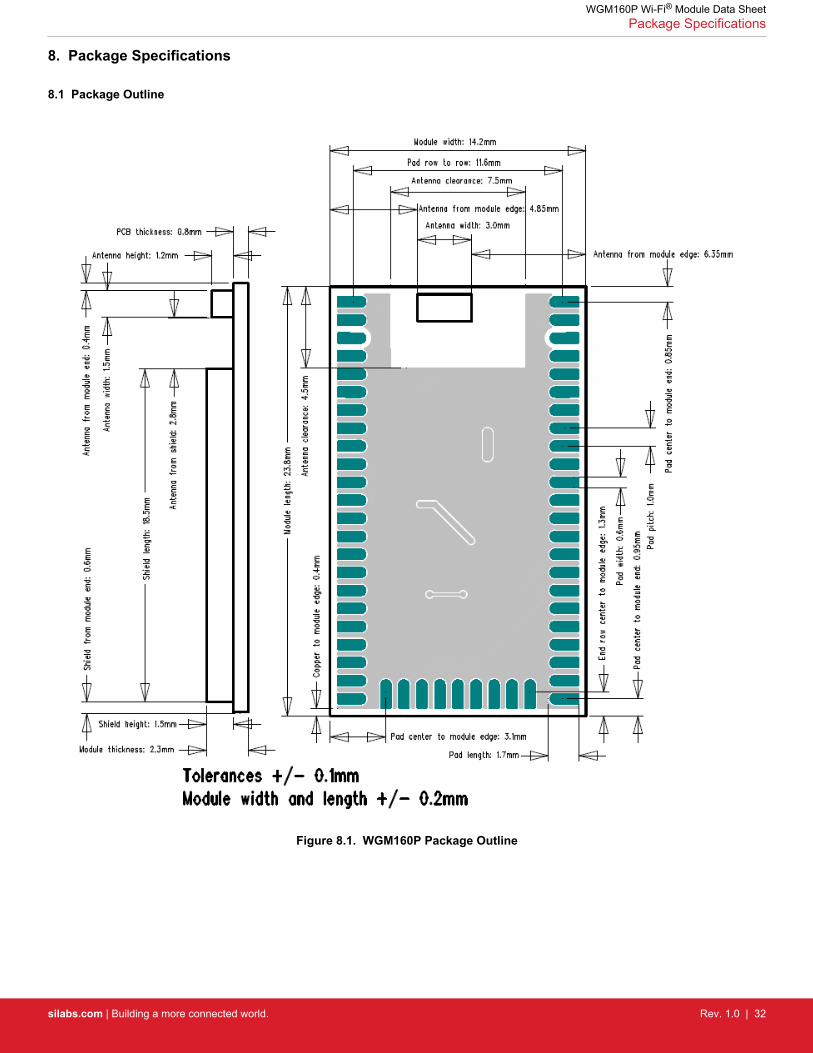
Figure 8.1. WGM160P Package Outline
WGM160P Wi-Fi® Module Data SheetPackage Specifications
silabs.com | Building a more connected world. Rev. 1.0 | 32
8.2 Recommended PCB Land Patterns
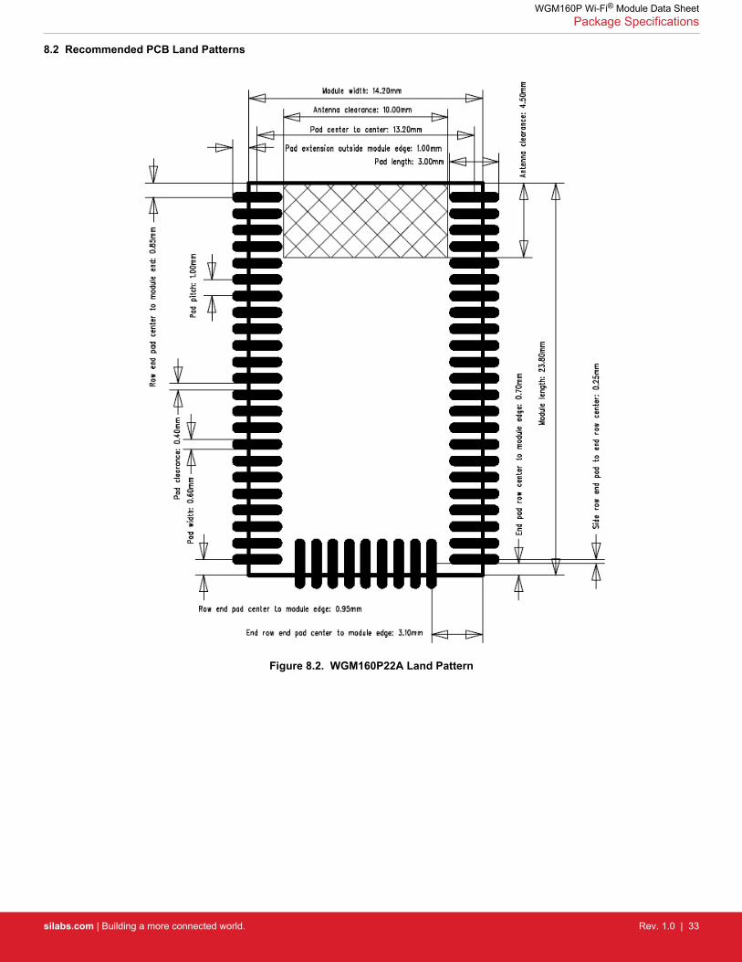
Figure 8.2. WGM160P22A Land Pattern
WGM160P Wi-Fi® Module Data SheetPackage Specifications
silabs.com | Building a more connected world. Rev. 1.0 | 33
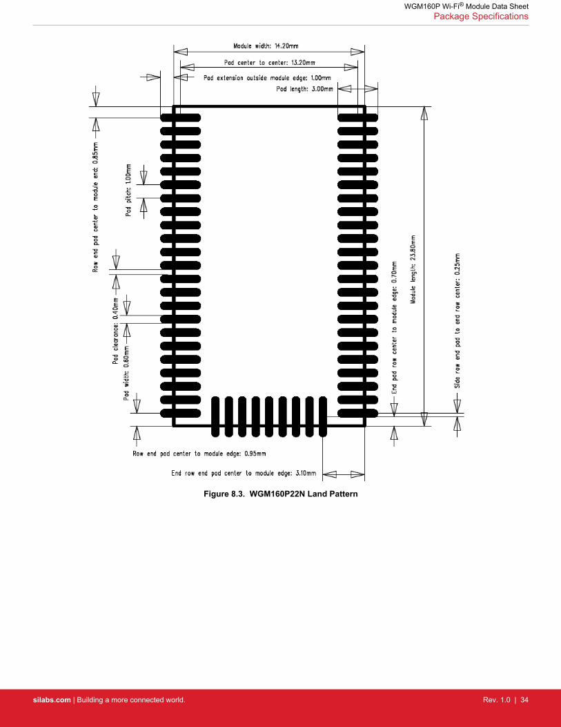
Figure 8.3. WGM160P22N Land Pattern
WGM160P Wi-Fi® Module Data SheetPackage Specifications
silabs.com | Building a more connected world. Rev. 1.0 | 34
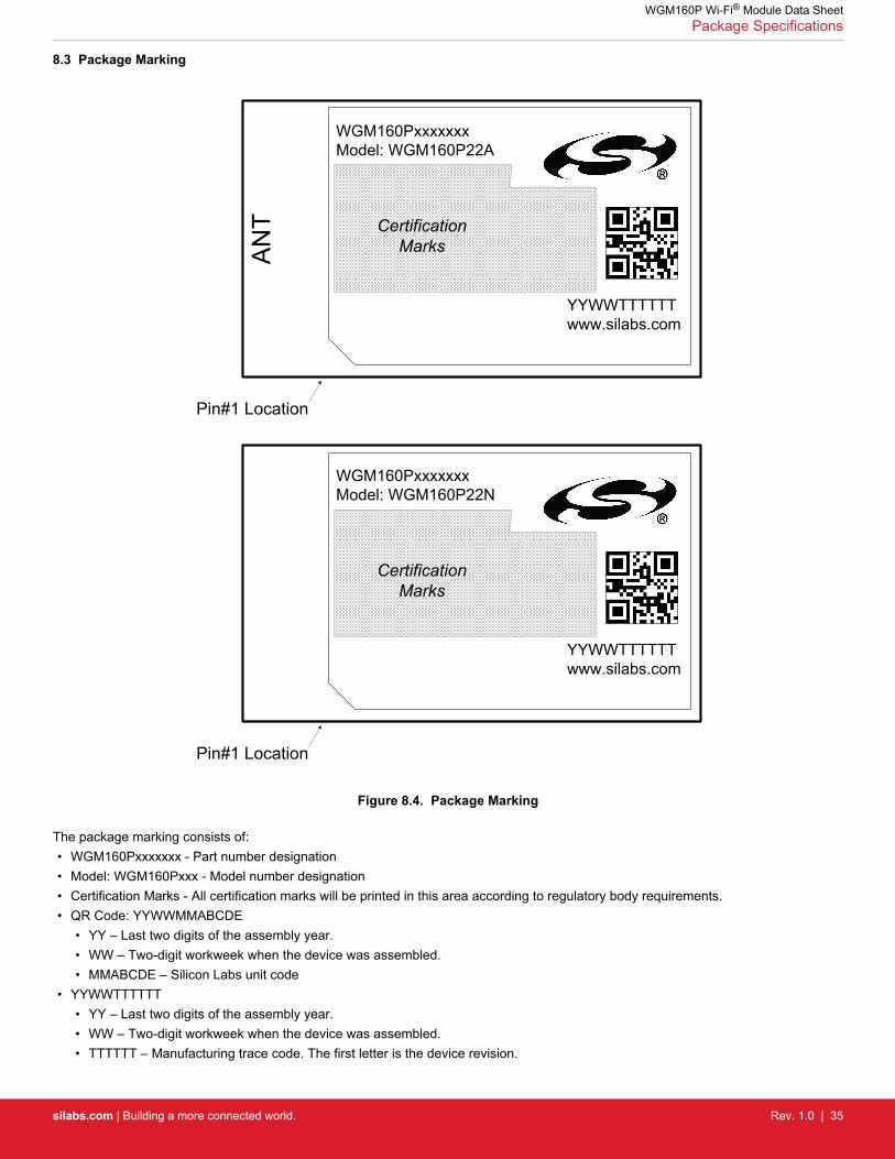
8.3 Package Marking
WGM160PxxxxxxxModel: WGM160P22A
YYWWTTTTTTwww.silabs.com
CertificationMarksA
NT
Pin#1 Location
WGM160PxxxxxxxModel: WGM160P22N
YYWWTTTTTTwww.silabs.com
CertificationMarks
Pin#1 Location
Figure 8.4. Package Marking
The package marking consists of:• WGM160Pxxxxxxx - Part number designation• Model: WGM160Pxxx - Model number designation• Certification Marks - All certification marks will be printed in this area according to regulatory body requirements.• QR Code: YYWWMMABCDE
• YY – Last two digits of the assembly year.• WW – Two-digit workweek when the device was assembled.• MMABCDE – Silicon Labs unit code
• YYWWTTTTTT• YY – Last two digits of the assembly year.• WW – Two-digit workweek when the device was assembled.• TTTTTT – Manufacturing trace code. The first letter is the device revision.
WGM160P Wi-Fi® Module Data SheetPackage Specifications
silabs.com | Building a more connected world. Rev. 1.0 | 35

9. Soldering Recommendations
It is recommended that final PCB assembly of this product follows the industry standard as identified by the Institute for Printed Circuits(IPC). This product is assembled in compliance with the J-STD-001 requirements and the guidelines of IPC-AJ-820. Surface mountingof this product by the end user is recommended to follow IPC-A-610 to meet or exceed class 2 requirements.
CLASS 1 General Electronic Products
Includes products suitable for applications where the major requirement is function of the completed assembly.
CLASS 2 Dedicated Service Electronic Products
Includes products where continued performance and extended life is required, and for which uninterrupted service is desired but notcritical. Typically the end-use environment would not cause failures.
CLASS 3 High Performance/Harsh Environment Electronic Products
Includes products where continued high performance or performance-on-demand is critical, equipment downtime cannot be tolerated,end-use environment may be uncommonly harsh, and the equipment must function when required, such as life support or other criticalsystems.
WGM160P Wi-Fi® Module Data SheetSoldering Recommendations
silabs.com | Building a more connected world. Rev. 1.0 | 36

10. Tape and Reel Dimensions
All dimensions in mm unless otherwise indicated.
Figure 10.1. Carrier Tape Dimensions
All dimensions in mm unless otherwise indicated.
Figure 10.2. Reel Dimensions
WGM160P Wi-Fi® Module Data SheetTape and Reel Dimensions
silabs.com | Building a more connected world. Rev. 1.0 | 37
11. Certifications
This section details certification status of the module in various regions.
The address for the module manufacturer and certification applicant is:
SILICON LABORATORIES FINLAND OYAlberga Business Park, Bertel Jungin aukio 3,02600 Espoo, Finland
11.1 Qualified External Antenna Types
This device has been certified with an integrated chip antenna as well as external antennas connected to either RF port or both. Therequired antenna impedance is 50 Ω.
Table 11.1. Qualified Antennas for WGM160P
Antenna Type Maximum Gain
Connectorized Coaxial Dipole 2.14 dBi
Any antenna of the same general type and of equal or less directional gain as listed in the above table can be used in the regulatoryareas that have a full modular radio approval (USA, Canada, Korea, Japan) as long as spot-check testing is performed to verify that noperformance changes compromising compliance have been introduced. In countries applying the ETSI standards, like the EU countries,the radiated emissions are always tested with the end-product and the antenna type is not critical, but antennas with higher gain mayviolate some of the regulatory limits.
If an antenna of a different type (such as a chip antenna, a PCB trace antenna or a patch) with a gain less than or equal to 2.14 dBi isneeded, it can be added as a permissive change, requiring some radiated emission testing. Antenna types with more gain than 2.14 dBimay require a fully new certification. Since the exact permissive change procedure is chosen on a case by case basis, please consultyour test house, for example while performing with them the EMC testing of the end-product.
11.2 CE
The WGM160P22A and WGM160P22N module is in conformity with the essential requirements and other relevant requirements of theRadio Equipment Directive (RED) (2014/53/EU). Please note that every application using the WGM160P22A and WGM160P22N willneed to perform the radio EMC tests on the end product, according to EN 301 489-17. It is ultimately the responsibility of the manufac-turer to ensure the compliance of the end-product. The specific product assembly may have an impact to RF radiated characteristics,and manufacturers should carefully consider RF radiated testing with the end-product assembly. A formal Declaration of Conformity(DoC) is available via https://www.silabs.com/products/wireless/wi-fi/wgm160p-wifi-module.
WGM160P Wi-Fi® Module Data SheetCertifications
silabs.com | Building a more connected world. Rev. 1.0 | 38

11.3 FCC
This device complies with Part 15 of the FCC Rules. Operation is subject to the following two conditions:1. This device may not cause harmful interference, and2. This device must accept any interference received, including interference that may cause undesirable operation.
Any changes or modifications not expressly approved by Silicon Labs could void the user’s authority to operate the equipment.
FCC RF Radiation Exposure Statement:
This equipment complies with FCC radiation exposure limits set forth for an uncontrolled environment. End users must follow the specif-ic operating instructions for satisfying RF exposure compliance. This transmitter meets both portable and mobile requirements in ac-cordance to the limits exposed in the RF Exposure Analysis. This transmitter must not be co-located or operating in conjunction withany other antenna or transmitter except in accordance with FCC multi-transmitter product procedures.
OEM Responsibilities to comply with FCC Regulations:
OEM integrator is responsible for testing their end-product for any additional compliance requirements needed with this module instal-led (for example, digital device emissions, PC peripheral requirements, etc.). Additionally, investigative measurements and spot check-ing are strongly recommended to verify that the full system compliance is maintained when the module is integrated, in accordance tothe "Host Product Testing Guidance" in FCC's KDB 996369 D04 Module Integration Guide V01.• In the typical case when the integral antenna of the WGM160P22A is used, a minimum separation distance of 40 mm must be main-
tained at all times between the human body and the radiator (antenna) to meet the SAR exemption for portable conditions. When theWGM160P22N is used instead, the minimum separation distance is also 40 mm, unless only the RF port 2 is used with a dipoleantenna, in which case the minimum distance is 37 mm.
• The transmitter module must not be co-located or operating in conjunction with any other antenna or transmitter except in accord-ance with FCC multi-transmitter product procedures.
Important Note:
In the event that these conditions cannot be met, then for the FCC authorization to remain valid the final product will have to undergoadditional testing to evaluate the RF exposure, and a permissive change will have to be applied with the help of the customer's ownTelecommunication Certification Body.
End Product Labeling
The variants of WGM160P Modules are labeled with their own FCC ID. If the FCC ID is not visible when the module is installed insideanother device, then the outside of the device into which the module is installed must also display a label referring to the enclosedmodule. In that case, the final end product must be labeled in a visible area with the following:
"Contains Transmitter Module FCC ID: QOQWGM160P"
Or
"Contains FCC ID: QOQWGM160P"
The OEM integrator has to be aware not to provide information to the end user regarding how to install or remove this RF module orchange RF related parameters in the user manual of the end product.
Class B Device Notice
Note: This equipment has been tested and found to comply with the limits for a Class B digital device, pursuant to part 15 of the FCCRules. These limits are designed to provide reasonable protection against harmful interference in a residential installation. This equip-ment generates, uses, and can radiate radio frequency energy and, if not installed and used in accordance with the instructions, maycause harmful interference to radio communications. However, there is no guarantee that interference will not occur in a particular in-stallation. If this equipment does cause harmful interference to radio or television reception, which can be determined by turning theequipment off and on, the user is encouraged to try to correct the interference by one or more of the following measures:• Reorient or relocate the receiving antenna• Increase the separation between the equipment and receiver• Connect the equipment into an outlet on a circuit different from that to which the receiver is connected• Consult the dealer or an experienced radio/TV technician for help
WGM160P Wi-Fi® Module Data SheetCertifications
silabs.com | Building a more connected world. Rev. 1.0 | 39

11.4 ISED Canada
ISED
This radio transmitter (IC: 5123A-WGM160P) has been approved by Innovation, Science and Economic Development Canada (ISEDCanada, formerly Industry Canada) to operate with the antenna types listed above, with the maximum permissible gain indicated. An-tenna types not included in this list, having a gain greater than the maximum gain listed, are strictly prohibited for use with this device.
This device complies with ISED’s license-exempt RSS standards. Operation is subject to the following two conditions:1. This device may not cause interference; and2. This device must accept any interference, including interference that may cause undesired operation of the device
RF Exposure Statement
Exemption from routine SAR evaluation limits are given in RSS-102 Issue 5.
The models WGM160P22A and WGM160P22N meet the given exemption requirements when the minimum separation distance be-tween the antenna(s) and the human body is respectively 30 mm and 40 mm. In the case of the N variant, the minimum separationdistance could also be 30 mm but only in the case of using exclusively the dipole antenna at RF port 2, without configuring any trans-mission out of RF port 1.
In other words, RF exposure or SAR evaluation is not required when the separation distance is same or more than stated above. If theseparation distance is less than stated above the OEM integrator is responsible for evaluating the SAR when using the module at itshighest transmission power.
OEM Responsibilities to comply with IC Regulations
The WGM160P modules have been certified for integration into products only by OEM integrators under the following conditions:• The antenna(s) must be installed such that a minimum separation distance as stated above is maintained between the radiator (an-
tenna) and all persons at all times.• The transmitter module must not be co-located or operating in conjunction with any other antenna or transmitter.
As long as the two conditions above are met, further transmitter testing will not be required. However, the OEM integrator is still respon-sible for testing their end-product for any additional compliance requirements required with this module installed (for example, digitaldevice emissions, PC peripheral requirements, etc.).
IMPORTANT NOTE
In the event that these conditions cannot be met, then for the ISED authorization to remain valid the final product will have to undergoadditional testing to evaluate the RF exposure, and a permissive change will have to be applied with the help of the customer's ownTelecommunication Certification Body.
End Product Labeling
The WGM160P module is labeled with its own ISED ID. If the ISED ID is not visible when the module is installed inside another device,then the outside of the device into which the module is installed must also display a label referring to the enclosed module. In that case,the final end product must be labeled in a visible area with the following:
“Contains Transmitter Module IC: 5123A-WGM160P ”
or
“Contains IC: 5123A-WGM160P”
The OEM integrator has to be aware not to provide information to the end user regarding how to install or remove this RF module orchange RF related parameters in the user manual of the end product.
CAN ICES-003 (B)
This Class B digital apparatus complies with Canadian ICES-003.
WGM160P Wi-Fi® Module Data SheetCertifications
silabs.com | Building a more connected world. Rev. 1.0 | 40

ISED (Français)
ISED a approuvé l’utilisation de cet émetteur radio (IC: 5123A-WGM160P) en conjonction avec des antennes de type dipolaire à2.14dBi ou de son antenne intégrée. L’utilisation de tout autre type d’antenne avec ce composant est proscrite.
Ce composant est conforme aux normes RSS, exonérées de licence d'ISED. Son mode de fonctionnement est soumis aux deux condi-tions suivantes:
1. Ce composant ne doit pas générer d’interférences.2. Ce composant doit pouvoir être soumis à tout type de perturbation y compris celle pouvant nuire à son bon fonctionnement.
Déclaration d'exposition RF
L'exemption tirée des limites courantes d'évaluation DAS est donnée dans le document RSS-102 Issue 5.
Les modèles WGM160P22A et WGM160P22N respectent les exigences d’exemption prévues lorsque la distance de séparation mini-male entre le(s) antenne(s) et le corps humain est respectivement de 30 mm et 40 mm. Dans le cas de la variante N, la distance mini-male de séparation pourrait également être de 30 mm, mais uniquement dans le cas d’une utilisation exclusive de l’antenne dipôle surle port RF 2, sans configurer de transmission sur le port RF 1.
La déclaration d’exposition RF ou l'évaluation DAS n'est pas nécessaire lorsque la distance de séparation est identique ou supérieure àcelle indiquée ci-dessus. Si la distance de séparation est inférieure à celle mentionnées plus haut, il incombe à l'intégrateur OEM deprocédé à une évaluation DAS.
Responsabilités des OEM pour une mise en conformité avec le Règlement du Circuit Intégré
Le module WGM160P a été approuvé pour l'intégration dans des produits finaux exclusivement réalisés par des OEM sous les condi-tions suivantes:• L'antenne (s) doit être installée de sorte qu'une distance de séparation minimale indiquée ci-dessus soit maintenue entre le radiateur
(antenne) et toutes les personnes avoisinante, ce à tout moment.• Le module émetteur ne doit pas être localisé ou fonctionner avec une autre antenne ou un autre transmetteur que celle indiquée
plus haut.
Tant que les deux conditions ci-dessus sont respectées, il n’est pas nécessaire de tester ce transmetteur de façon plus poussée. Ce-pendant, il incombe à l’intégrateur OEM de s’assurer de la bonne conformité du produit fini avec les autres normes auxquelles il pour-rait être soumis de fait de l’utilisation de ce module (par exemple, les émissions des périphériques numériques, les exigences de pé-riphériques PC, etc.).
REMARQUE IMPORTANTE
Dans le cas où ces conditions ne peuvent être satisfaites (pour certaines configurations ou co-implantation avec un autre émetteur),l'autorisation ISED n'est plus considérée comme valide et le numéro d’identification ID IC ne peut pas être apposé sur le produit final.Dans ces circonstances, l'intégrateur OEM sera responsable de la réévaluation du produit final (y compris le transmetteur) et de l'ob-tention d'une autorisation ISED distincte.
Étiquetage des produits finis
Les modules WGM160P sont étiquetés avec leur propre ID ISED. Si l'ID ISED n'est pas visible lorsque le module est intégré au seind'un autre produit, cet autre produit dans lequel le module est installé devra porter une étiquette faisant apparaitre la référence du mod-ule intégré. Dans un tel cas, sur le produit final doit se trouver une étiquette aisément lisible sur laquelle figurent les informations sui-vantes:
“Contient le module transmetteur IC: 5123A-WGM160P ”
ou
“Contient le circuit IC: 5123A-WGM160P”
L'intégrateur OEM doit être conscient qu’il ne doit pas fournir, dans le manuel d’utilisation, d'informations relatives à la façon d'installerou de d’enlever ce module RF ainsi que sur la procédure à suivre pour modifier les paramètres liés à la radio.
WGM160P Wi-Fi® Module Data SheetCertifications
silabs.com | Building a more connected world. Rev. 1.0 | 41
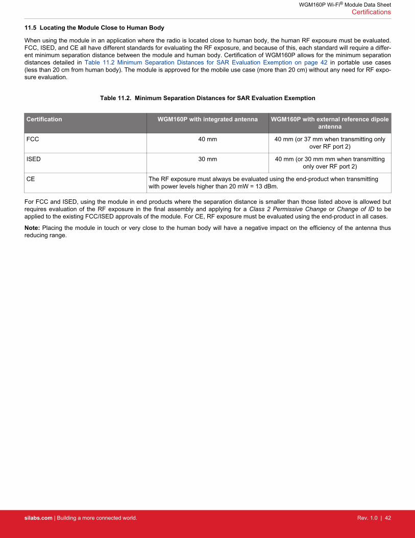
11.5 Locating the Module Close to Human Body
When using the module in an application where the radio is located close to human body, the human RF exposure must be evaluated.FCC, ISED, and CE all have different standards for evaluating the RF exposure, and because of this, each standard will require a differ-ent minimum separation distance between the module and human body. Certification of WGM160P allows for the minimum separationdistances detailed in Table 11.2 Minimum Separation Distances for SAR Evaluation Exemption on page 42 in portable use cases(less than 20 cm from human body). The module is approved for the mobile use case (more than 20 cm) without any need for RF expo-sure evaluation.
Table 11.2. Minimum Separation Distances for SAR Evaluation Exemption
Certification WGM160P with integrated antenna WGM160P with external reference dipoleantenna
FCC 40 mm 40 mm (or 37 mm when transmitting onlyover RF port 2)
ISED 30 mm 40 mm (or 30 mm mm when transmittingonly over RF port 2)
CE The RF exposure must always be evaluated using the end-product when transmittingwith power levels higher than 20 mW = 13 dBm.
For FCC and ISED, using the module in end products where the separation distance is smaller than those listed above is allowed butrequires evaluation of the RF exposure in the final assembly and applying for a Class 2 Permissive Change or Change of ID to beapplied to the existing FCC/ISED approvals of the module. For CE, RF exposure must be evaluated using the end-product in all cases.
Note: Placing the module in touch or very close to the human body will have a negative impact on the efficiency of the antenna thusreducing range.
WGM160P Wi-Fi® Module Data SheetCertifications
silabs.com | Building a more connected world. Rev. 1.0 | 42
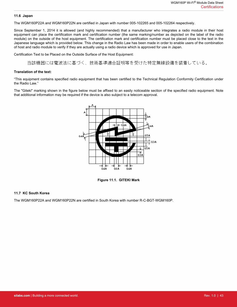
11.6 Japan
The WGM160P22A and WGM160P22N are certified in Japan with number 005-102265 and 005-102264 respectively.
Since September 1, 2014 it is allowed (and highly recommended) that a manufacturer who integrates a radio module in their hostequipment can place the certification mark and certification number (the same marking/number as depicted on the label of the radiomodule) on the outside of the host equipment. The certification mark and certification number must be placed close to the text in theJapanese language which is provided below. This change in the Radio Law has been made in order to enable users of the combinationof host and radio module to verify if they are actually using a radio device which is approved for use in Japan.
Certification Text to be Placed on the Outside Surface of the Host Equipment:
Translation of the text:
“This equipment contains specified radio equipment that has been certified to the Technical Regulation Conformity Certification underthe Radio Law.”
The "Giteki" marking shown in the figure below must be affixed to an easily noticeable section of the specified radio equipment. Notethat additional information may be required if the device is also subject to a telecom approval.
Figure 11.1. GITEKI Mark
11.7 KC South Korea
The WGM160P22A and WGM160P22N are certified in South Korea with number R-C-BGT-WGM160P.
WGM160P Wi-Fi® Module Data SheetCertifications
silabs.com | Building a more connected world. Rev. 1.0 | 43

12. Revision History
Revision 1.0
March 2020• Removed WiFi Alliance from certifications listed in Front Page and Key Features• Added note to Table 3.1 Supported Wi-Fi Modulations, BW, and Channels on page 6• Added DTIM and sleep current values to Table 4.3 Power Consumption on page 8 and updated Typical standby current from 638 nA
to 217 nA• Updated Max VOL from 20 to 25 % and Min VOH from 80 to 75% in 4.4 Digital I/O Specifications• Added note about peripherals supported by GeckoOS in 4.8 Microcontroller Peripherals• Added reference to AN1224 in 5.2 Multi-Protocol Coexistence• Corrected pin 40 naming from VUSB to VSUB in Figure 5.1• Added 11.6 Japan and 11.7 KC South Korea certifications
Revision 0.5
April 2019• Updated naming for Sections 7.2 GPIO Functionality and 7.3 Alternate Pin Functionality• Removed TBD Idle currents from Table 4.3 Power Consumption on page 8 and changed term "Sleep" to "Standby"• Updated Table 4.4 Digital I/O Specifications on page 9• Updated Table 4.6 RF Receiver Characteristics on page 11• Updated min PCBx_mm to 40 mm in Table 4.7 Radiated Characteristics on page 11• Updated Section 9. Soldering Recommendations• Updated module manufacturer address in Section 11. Certifications• Updated text in Sections 11.1 Qualified External Antenna Types, 11.3 FCC, 11.4 ISED Canada, and 11.5 Locating the Module Close
to Human Body• Updated Table 11.2 Minimum Separation Distances for SAR Evaluation Exemption on page 42
Revision 0.3
Feb 2019• Updated top-level device details throughout document.• Removed software details from Section 1. Key Features (moved to Section 6. Gecko OS Features).• Updated Section 2. Ordering Information to expand all OPN details.• Corrected details in Section Figure 3.1 WGM160P Block Diagram on page 6.• Updated all tables in Section 4. Electrical Specifications with latest nomenclature and characterization data.• Added Section 5.3 Example Schematic.• Added Section 6. Gecko OS Features.• Updated pinout details in Section 7. Pin Descriptions.• Removed functions not pinned out from Section 7.2 GPIO Functionality and 7.3 Alternate Pin Functionality.• Updated Section 8. Package Specifications with additional landing diagram and package marking details.• Added Section 9. Soldering Recommendations.• Added Section 10. Tape and Reel Dimensions.• Added Section 11. Certifications.
Revision 0.2
November 2018• Initial release.
WGM160P Wi-Fi® Module Data SheetRevision History
silabs.com | Building a more connected world. Rev. 1.0 | 44

Simplicity StudioOne-click access to MCU and wireless tools, documentation, software, source code libraries & more. Available for Windows, Mac and Linux!
IoT Portfoliowww.silabs.com/IoT
SW/HWwww.silabs.com/simplicity
Qualitywww.silabs.com/quality
Support and Communitycommunity.silabs.com
http://www.silabs.com
Silicon Laboratories Inc.400 West Cesar ChavezAustin, TX 78701USA
DisclaimerSilicon Labs intends to provide customers with the latest, accurate, and in-depth documentation of all peripherals and modules available for system and software implementers using or intending to use the Silicon Labs products. Characterization data, available modules and peripherals, memory sizes and memory addresses refer to each specific device, and "Typical" parameters provided can and do vary in different applications. Application examples described herein are for illustrative purposes only. Silicon Labs reserves the right to make changes without further notice to the product information, specifications, and descriptions herein, and does not give warranties as to the accuracy or completeness of the included information. Without prior notification, Silicon Labs may update product firmware during the manufacturing process for security or reliability reasons. Such changes will not alter the specifications or the performance of the product. Silicon Labs shall have no liability for the consequences of use of the information supplied in this document. This document does not imply or expressly grant any license to design or fabricate any integrated circuits. The products are not designed or authorized to be used within any FDA Class III devices, applications for which FDA premarket approval is required, or Life Support Systems without the specific written consent of Silicon Labs. A "Life Support System" is any product or system intended to support or sustain life and/or health, which, if it fails, can be reasonably expected to result in significant personal injury or death. Silicon Labs products are not designed or authorized for military applications. Silicon Labs products shall under no circumstances be used in weapons of mass destruction including (but not limited to) nuclear, biological or chemical weapons, or missiles capable of delivering such weapons. Silicon Labs disclaims all express and implied warranties and shall not be responsible or liable for any injuries or damages related to use of a Silicon Labs product in such unauthorized applications.
Trademark InformationSilicon Laboratories Inc.®, Silicon Laboratories®, Silicon Labs®, SiLabs® and the Silicon Labs logo®, Bluegiga®, Bluegiga Logo®, ClockBuilder®, CMEMS®, DSPLL®, EFM®, EFM32®, EFR, Ember®, Energy Micro, Energy Micro logo and combinations thereof, "the world’s most energy friendly microcontrollers", Ember®, EZLink®, EZRadio®, EZRadioPRO®, Gecko®, Gecko OS, Gecko OS Studio, ISOmodem®, Precision32®, ProSLIC®, Simplicity Studio®, SiPHY®, Telegesis, the Telegesis Logo®, USBXpress® , Zentri, the Zentri logo and Zentri DMS, Z-Wave®, and others are trademarks or registered trademarks of Silicon Labs. ARM, CORTEX, Cortex-M3 and THUMB are trademarks or registered trademarks of ARM Holdings. Keil is a registered trademark of ARM Limited. Wi-Fi is a registered trademark of the Wi-Fi Alliance. All other products or brand names mentioned herein are trademarks of their respective holders.


![OdakyuAndroid t Google play] Wi-Fi Android ios t App Store] Wi-Fi [App Store] [iPhone Profile) Wi-Fi # —E Odakyu Odakyu Free Wi-Fi Android [Google play] WI-Fi Android [App Wi-Fi](https://img.pdfslide.net/doc/110x75/5fcc31f69b77e950d81a9828/android-t-google-play-wi-fi-android-ios-t-app-store-wi-fi-app-store-iphone.jpg)


![2 Pilih [Wi-Fi function (Fungsi Wi-Fi)]](https://img.pdfslide.net/doc/110x75/587653b01a28ab135e8b9be3/2-pilih-wi-fi-function-fungsi-wi-fi.jpg)
