Embed Size (px)
Citation preview
Analog Dialogue 50-11, November 2016 1
What’s Up with Digital Downconverters— Part 2By Jonathan Harris
Share on
We will begin by looking at the DDC decimation filters when the complex to real conversion block is enabled in the AD9680. This means the DDC will be configured to accept a real input and have a real output. In the AD9680, the complex to real conversion automatically shifts the input frequencies up in frequency by an amount equal to fS/4. Figure 2 shows the low-pass response of the HB1 filter. This is the response of HB1 showing the real and complex domain response. In order to understand the real operation of the filter it is important to first see the basic filter response in the real and complex domains so that the low-pass response can be seen. The HB1 filter has a pass band of 38.5% of the real Nyquist zone. It also has a stop band that is 38.5% of the real Nyquist zone with the transition band making up the remaining 23%. Likewise in the complex domain, the pass band and stop band each make up 38.5% (77% total) of the complex Nyquist zone with the transition band making up the remaining 23%. As Figure 2 illus-trates, the filter is a mirror image between the real and complex domains.
–fS/2 –fS/4 fS/4
–100 dB
38.5% fS/2>100 dB
38.5% –fS/2<0.001 dB
38.5% fS/2<0.001 dB
0 fS/2
Figure 2. HB1 filter response—real and complex domain response.
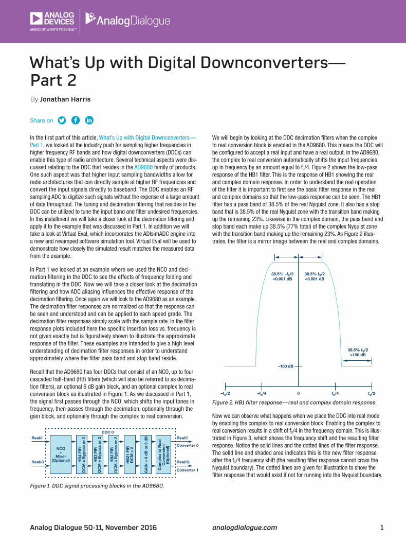
Now we can observe what happens when we place the DDC into real mode by enabling the complex to real conversion block. Enabling the complex to real conversion results in a shift of fS/4 in the frequency domain. This is illus-trated in Figure 3, which shows the frequency shift and the resulting filter response. Notice the solid lines and the dotted lines of the filter response. The solid line and shaded area indicates this is the new filter response after the fS/4 frequency shift (the resulting filter response cannot cross the Nyquist boundary). The dotted lines are given for illustration to show the filter response that would exist if not for running into the Nyquist boundary.
analogdialogue.com
In the first part of this article, What’s Up with Digital Downconverters— Part 1, we looked at the industry push for sampling higher frequencies in higher frequency RF bands and how digital downconverters (DDCs) can enable this type of radio architecture. Several technical aspects were dis-cussed relating to the DDC that resides in the AD9680 family of products. One such aspect was that higher input sampling bandwidths allow for radio architectures that can directly sample at higher RF frequencies and convert the input signals directly to baseband. The DDC enables an RF sampling ADC to digitize such signals without the expense of a large amount of data throughput. The tuning and decimation filtering that resides in the DDC can be utilized to tune the input band and filter undesired frequencies. In this installment we will take a closer look at the decimation filtering and apply it to the example that was discussed in Part 1. In addition we will take a look at Virtual Eval, which incorporates the ADIsimADC engine into a new and revamped software simulation tool. Virtual Eval will be used to demonstrate how closely the simulated result matches the measured data from the example.
In Part 1 we looked at an example where we used the NCO and deci-mation filtering in the DDC to see the effects of frequency folding and translating in the DDC. Now we will take a closer look at the decimation filtering and how ADC aliasing influences the effective response of the decimation filtering. Once again we will look to the AD9680 as an example. The decimation filter responses are normalized so that the response can be seen and understood and can be applied to each speed grade. The decimation filter responses simply scale with the sample rate. In the filter response plots included here the specific insertion loss vs. frequency is not given exactly but is figuratively shown to illustrate the approximate response of the filter. These examples are intended to give a high level understanding of decimation filter responses in order to understand approximately where the filter pass band and stop band reside.
Recall that the AD9680 has four DDCs that consist of an NCO, up to four cascaded half-band (HB) filters (which will also be referred to as decima-tion filters), an optional 6 dB gain block, and an optional complex to real conversion block as illustrated in Figure 1. As we discussed in Part 1, the signal first passes through the NCO, which shifts the input tones in frequency, then passes through the decimation, optionally through the gain block, and optionally through the complex to real conversion.
Real/I
NCO+
Mixer(Optional) H
B4
FIR
DC
M =
Byp
ass
or
2
HB
3 FI
RD
CM
= B
ypas
s o
r 2
HB
2 FI
RD
CM
= B
ypas
s o
r 2
HB
21 F
IRD
CM
= 2
GA
IN =
0 d
B o
r 6
dB
Co
mp
lex
to R
eal
Co
nver
sio
n(O
pti
ona
l)
DDC 0
Real/Q
Real/I
Real/Q
Converter 0
Converter 1
Figure 1. DDC signal processing blocks in the AD9680.
Analog Dialogue 50-11, November 2016 2
77% fS/2<0.001 dB
ComplexPortion
Discarded
–fS/4 fS/40 fS/2 3fS/2
–100 dB
Figure 3. HB1 filter response—real DDC mode (complex to real conversion enabled).
Notice that the HB1 filter bandwidth remains unchanged between Figures 2 and 3. The difference between the two is the fS/4 frequency shift and the resultant center frequency within the first Nyquist zone. Notice, however, that in Figure 2 we have 38.5% of Nyquist for the real portion of the signal and 38.5% of Nyquist for the complex portion of the signal. In Figure 3 with the complex to real conversion block enabled there is 77% of Nyquist for the real signal and the complex domain has been discarded. The filter response remains unchanged apart from the fS/4 frequency shift. Also, notice as a product of this conversion that the decimation rate is now equal to one. The effective sample rate is still fS but instead of the entire Nyquist zone there is only 77% of available bandwidth in the Nyquist zone. This means that with the HB1 filter and the complex to real conversion block enabled the decimation rate equals one (see the AD9680 data sheet for more information).
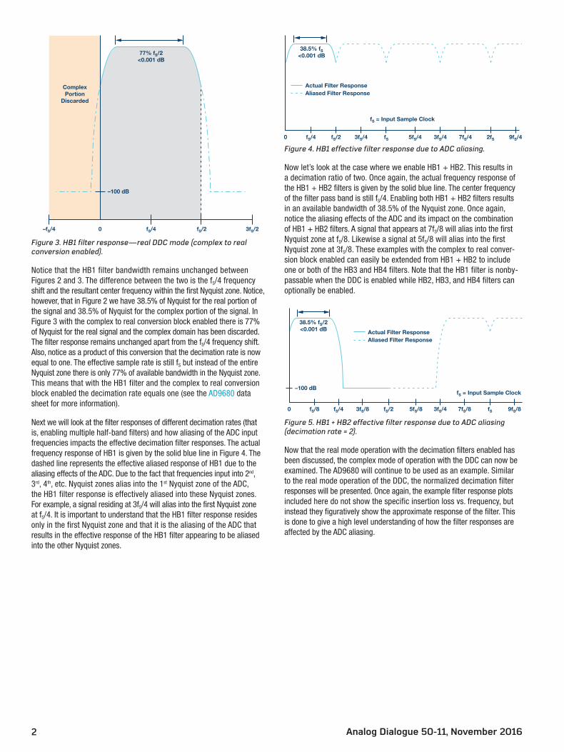
Next we will look at the filter responses of different decimation rates (that is, enabling multiple half-band filters) and how aliasing of the ADC input frequencies impacts the effective decimation filter responses. The actual frequency response of HB1 is given by the solid blue line in Figure 4. The dashed line represents the effective aliased response of HB1 due to the aliasing effects of the ADC. Due to the fact that frequencies input into 2nd, 3rd, 4th, etc. Nyquist zones alias into the 1st Nyquist zone of the ADC, the HB1 filter response is effectively aliased into these Nyquist zones. For example, a signal residing at 3fS/4 will alias into the first Nyquist zone at fS/4. It is important to understand that the HB1 filter response resides only in the first Nyquist zone and that it is the aliasing of the ADC that results in the effective response of the HB1 filter appearing to be aliased into the other Nyquist zones.
fS/40 fS/2 3fS/4 fS
fS = Input Sample Clock
Actual Filter ResponseAliased Filter Response
5fS/4 3fS/4 7fS/4 2fS 9fS/4
38.5% fS<0.001 dB
Figure 4. HB1 effective filter response due to ADC aliasing.
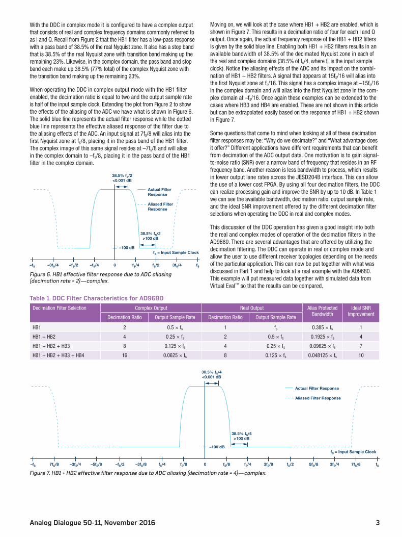
Now let’s look at the case where we enable HB1 + HB2. This results in a decimation ratio of two. Once again, the actual frequency response of the HB1 + HB2 filters is given by the solid blue line. The center frequency of the filter pass band is still fS/4. Enabling both HB1 + HB2 filters results in an available bandwidth of 38.5% of the Nyquist zone. Once again, notice the aliasing effects of the ADC and its impact on the combination of HB1 + HB2 filters. A signal that appears at 7fS/8 will alias into the first Nyquist zone at fS/8. Likewise a signal at 5fS/8 will alias into the first Nyquist zone at 3fS/8. These examples with the complex to real conver-sion block enabled can easily be extended from HB1 + HB2 to include one or both of the HB3 and HB4 filters. Note that the HB1 filter is nonby-passable when the DDC is enabled while HB2, HB3, and HB4 filters can optionally be enabled.
fS/8
–100 dB
0 fS/4 3fS/8 fS/2 5fS/8 3fS/4 7fS/8 fS 9fS/8
fS = Input Sample Clock
Actual Filter ResponseAliased Filter Response
38.5% fS/2<0.001 dB
Figure 5. HB1 + HB2 effective filter response due to ADC aliasing (decimation rate = 2).
Now that the real mode operation with the decimation filters enabled has been discussed, the complex mode of operation with the DDC can now be examined. The AD9680 will continue to be used as an example. Similar to the real mode operation of the DDC, the normalized decimation filter responses will be presented. Once again, the example filter response plots included here do not show the specific insertion loss vs. frequency, but instead they figuratively show the approximate response of the filter. This is done to give a high level understanding of how the filter responses are affected by the ADC aliasing.
Analog Dialogue 50-11, November 2016 3
With the DDC in complex mode it is configured to have a complex output that consists of real and complex frequency domains commonly referred to as I and Q. Recall from Figure 2 that the HB1 filter has a low-pass response with a pass band of 38.5% of the real Nyquist zone. It also has a stop band that is 38.5% of the real Nyquist zone with transition band making up the remaining 23%. Likewise, in the complex domain, the pass band and stop band each make up 38.5% (77% total) of the complex Nyquist zone with the transition band making up the remaining 23%.
When operating the DDC in complex output mode with the HB1 filter enabled, the decimation ratio is equal to two and the output sample rate is half of the input sample clock. Extending the plot from Figure 2 to show the effects of the aliasing of the ADC we have what is shown in Figure 6. The solid blue line represents the actual filter response while the dotted blue line represents the effective aliased response of the filter due to the aliasing effects of the ADC. An input signal at 7fS/8 will alias into the first Nyquist zone at fS/8, placing it in the pass band of the HB1 filter. The complex image of this same signal resides at –7fS/8 and will alias in the complex domain to –fS/8, placing it in the pass band of the HB1 filter in the complex domain.
38.5% fS/2<0.001 dB
fS = Input Sample Clock
Actual Filter Response
Aliased Filter Response
–100 dB
38.5% fS/2>100 dB
–fS –3fS/4 –fS/4 fS/4 fS/2 3fS/4 fS0–fS/2
Figure 6. HB1 effective filter response due to ADC aliasing (decimation rate = 2)—complex.
Moving on, we will look at the case where HB1 + HB2 are enabled, which is shown in Figure 7. This results in a decimation ratio of four for each I and Q output. Once again, the actual frequency response of the HB1 + HB2 filters is given by the solid blue line. Enabling both HB1 + HB2 filters results in an available bandwidth of 38.5% of the decimated Nyquist zone in each of the real and complex domains (38.5% of fS/4, where fS is the input sample clock). Notice the aliasing effects of the ADC and its impact on the combi-nation of HB1 + HB2 filters. A signal that appears at 15fS/16 will alias into the first Nyquist zone at fS/16. This signal has a complex image at –15fS/16 in the complex domain and will alias into the first Nyquist zone in the com-plex domain at –fS/16. Once again these examples can be extended to the cases where HB3 and HB4 are enabled. These are not shown in this article but can be extrapolated easily based on the response of HB1 + HB2 shown in Figure 7.
Some questions that come to mind when looking at all of these decimation filter responses may be: “Why do we decimate?” and “What advantage does it offer?” Different applications have different requirements that can benefit from decimation of the ADC output data. One motivation is to gain signal-to-noise ratio (SNR) over a narrow band of frequency that resides in an RF frequency band. Another reason is less bandwidth to process, which results in lower output lane rates across the JESD204B interface. This can allow the use of a lower cost FPGA. By using all four decimation filters, the DDC can realize processing gain and improve the SNR by up to 10 dB. In Table 1 we can see the available bandwidth, decimation ratio, output sample rate, and the ideal SNR improvement offered by the different decimation filter selections when operating the DDC in real and complex modes.
This discussion of the DDC operation has given a good insight into both the real and complex modes of operation of the decimation filters in the AD9680. There are several advantages that are offered by utilizing the decimation filtering. The DDC can operate in real or complex mode and allow the user to use different receiver topologies depending on the needs of the particular application. This can now be put together with what was discussed in Part 1 and help to look at a real example with the AD9680. This example will put measured data together with simulated data from Virtual Eval™ so that the results can be compared.
38.5% fS/4<0.001 dB
fS = Input Sample Clock
Actual Filter Response
Aliased Filter Response
–100 dB
38.5% fS/4>100 dB
–fS 7fS/8 –5fS/8 5fS/8 3fS/4 7fS/8 fS–3fS/8 3fS/8fS/4 fS/4fS/8 fS/80–fS/2 fS/2–3fS/4
Figure 7. HB1 + HB2 effective filter response due to ADC aliasing (decimation rate = 4)—complex.
Table 1. DDC Filter Characteristics for AD9680
Decimation Filter Selection Complex Output Real Output Alias Protected Bandwidth
Ideal SNR Improvement
Decimation Ratio Output Sample Rate Decimation Ratio Output Sample Rate
HB1 2 0.5 × fS 1 fS 0.385 × fS 1
HB1 + HB2 4 0.25 × fS 2 0.5 × fS 0.1925 × fS 4
HB1 + HB2 + HB3 8 0.125 × fS 4 0.25 × fS 0.09625 × fS 7
HB1 + HB2 + HB3 + HB4 16 0.0625 × fS 8 0.125 × fS 0.048125 × fS 10
Analog Dialogue 50-11, November 2016 4
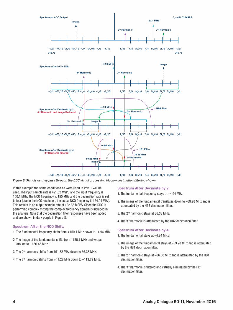
In this example the same conditions as were used in Part 1 will be used. The input sample rate is 491.52 MSPS and the input frequency is 150.1 MHz. The NCO frequency is 155 MHz and the decimation rate is set to four (due to the NCO resolution, the actual NCO frequency is 154.94 MHz). This results in an output sample rate of 122.88 MSPS. Since the DDC is performing complex mixing the complex frequency domain is included in the analysis. Note that the decimation filter responses have been added and are shown in dark purple in Figure 8.
Spectrum After the NCO Shift:1. The fundamental frequency shifts from +150.1 MHz down to –4.94 MHz.
2. The image of the fundamental shifts from –150.1 MHz and wraps around to +186.48 MHz.
3. The 2nd harmonic shifts from 191.32 MHz down to 36.38 MHz.
4. The 3rd harmonic shifts from +41.22 MHz down to –113.72 MHz.
Spectrum After Decimate by 2:1. The fundamental frequency stays at –4.94 MHz.
2. The image of the fundamental translates down to –59.28 MHz and is attenuated by the HB2 decimation filter.
3. The 2nd harmonic stays at 36.38 MHz.
4. The 3rd harmonic is attenuated by the HB2 decimation filter.
Spectrum After Decimate by 4:1. The fundamental stays at –4.94 MHz.
2. The image of the fundamental stays at –59.28 MHz and is attenuated by the HB1 decimation filter.
3. The 2nd harmonic stays at –36.38 MHz and is attenuated by the HB1 decimation filter.
4. The 3rd harmonic is filtered and virtually eliminated by the HB1 decimation filter.
Spectrum at ADC Output
Image
Image
3rd Harmonic 2nd Harmonic
150.1 MHzfs = 491.52 MSPS
Spectrum After NCO Shift
Spectrum After Decimate by 23rd Harmonic and Image Reduced
Spectrum After Decimate by 43rd Harmonic Filtered
–fs/2 –7fs/16 –3fs/8 –5fs/16 –fs/4 –3fs/16 –fs/8 –fs/16 fs/16 fs/8 3fs/16 fs/4 5fs/16 3fs/8 7fs/16 fs/2
245.76–245.76
–fs/2 –7fs/16 –5fs/16 –fs/4 –3fs/16 –fs/8 –fs/16 fs/8 3fs/16 fs/4 5fs/16 7fs/16 fs/2
–fs/2 –7fs/16 –3fs/8 –5fs/16 –fs/4 –fs/16 fs/16 fs/8 fs/4 5fs/16 3fs/8 7fs/16 fs/2
–fs/2 –7fs/16 –3fs/8 –5fs/16 –fs/4 –3fs/16 –fs/8 –fs/16 fs/16 fs/8 3fs/16 fs/4 5fs/16 3fs/8 7fs/16 fs/2
3rd Harmonic 2nd Harmonic
2nd Harmonic
–4.94 MHz
–4.94 MHz
–4.94 MHz
36.38 MHz
Image
fs/16
–fs/8
HB2 Filter
HB1 Filter
3rd Harmonic
–59.28 MHzImage
2nd Harmonic
–3fs/16 3fs/16
–3fs/8 3fs/8
Figure 8. Signals as they pass through the DDC signal processing block—decimation filtering shown.

Analog Dialogue 50-11, November 2016 5
The actual measurement on the AD9680-500 is shown in Figure 9. The fundamental frequency is at –4.94 MHz. The image of the fundamental resides at –59.28 MHz with an amplitude of –67.112 dBFS, which means that the image has been attenuated by approximately 66 dB. The 2nd harmonic resides at 36.38 MHz and has been attenuated by approximately 10 dB to 15 dB. The 3rd harmonic has been filtered sufficiently that it does not rise above the noise floor in the measurement.
–4.94 MHz
–59.28 MHz
36.38 MHz
–4.94 MHz
–59.28 MHz
36.38 MHz
Figure 9. FFT complex output of signal after DDC with NCO = 155 MHz and decimate by 4.
Now Virtual Eval can be used to see how the simulated results compare to the measured results. To begin, open the tool from the website and select an ADC to simulate (see Figure 10). The Virtual Eval tool is on the Analog Devices website at Virtual Eval. The AD9680 model that resides in Virtual Eval incorporates a new feature being developed that allows the user to simulate different speed grades of ADCs. This feature is key to the example since the example utilizes the AD9680-500. Once Virtual Eval loads, the first prompt is to select a product category and a product. Notice that Virtual Eval not only covers high speed ADCs but also has product categories for precision ADCs, high speed DACs, and integrated/special purpose converters.
Figure 10. Product category and product selection in Virtual Eval.
Select the AD9680 from the product selection. This will open up the main page for the simulation of the AD9680. The Virtual Eval model for the AD9680 also includes a block diagram that gives details on the internal configuration of the ADC analog and digital features. This block diagram is the same as the one given in the data sheet for the AD9680. From this page select the desired speed grade from the drop-down menu on the left side of the page. For the example here, select the 500 MHz speed grade as shown in Figure 11.
Figure 11. AD9680 speed grade selection and block diagram in Virtual Eval.
Next, the input conditions must be set in order to perform the FFT simu-lation (see Figure 12). Recall the test conditions for the example include a clock rate of 491.52 MHz and an input frequency of 150 MHz. The DDC is enabled with the NCO frequency set to 155 MHz, the ADC input is set to Real, the complex to real conversion (C2R) is Disabled, the DDC decimation rate is set to Four, and the 6 dB gain in the DDC is Enabled. This means the DDC is set up for a real input signal and a complex output signal with a decimation ratio of four. The 6 dB gain in the DDC is enabled in order to compensate for the 6 dB loss due to the mixing process in the DDC. Virtual Eval will show only noise or distortion results at a time, so two plots are included where one shows the noise results (Figure 12) and the other shows the distortion results (Figure 13).
Figure 12. AD9680 FFT simulation in Virtual Eval—noise results.
Figure 13. AD9680 FFT simulation in Virtual Eval—distortion results.
Analog Dialogue 50-11, November 2016 6
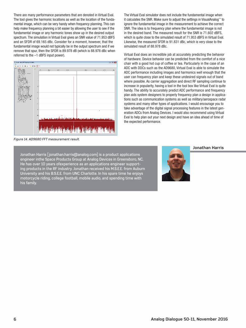
There are many performance parameters that are denoted in Virtual Eval. The tool gives the harmonic locations as well as the location of the funda-mental image, which can be very handy when frequency planning. This can help make frequency planning a bit easier by allowing the user to see if the fundamental image or any harmonic tones show up in the desired output spectrum. The simulation in Virtual Eval gives an SNR value of 71.953 dBFS and an SFDR of 69.165 dBc. Consider for a moment, however, that the fundamental image would not typically be in the output spectrum and if we remove that spur, then the SFDR is 89.978 dB (which is 88.978 dBc when referred to the –1 dBFS input power).
Figure 14. AD9680 FFT measurement result.
The Virtual Eval simulator does not include the fundamental image when it calculates the SNR. Make sure to adjust the settings in VisualAnalog™ to ignore the fundamental image in the measurement to achieve the correct SNR. The idea is to frequency plan where the fundamental image is not in the desired band. The measured result for the SNR is 71.602 dBFS, which is quite close to the simulated result of 71.953 dBFS in Virtual Eval. Likewise, the measured SFDR is 91.831 dBc, which is very close to the simulated result of 88.978 dBc.
Virtual Eval does an incredible job at accurately predicting the behavior of hardware. Device behavior can be predicted from the comfort of a nice chair with a good hot cup of coffee or tea. Particularly in the case of an ADC with DDCs such as the AD9680, Virtual Eval is able to simulate the ADC performance including images and harmonics well enough that the user can frequency plan and keep these undesired signals out of band where possible. As carrier aggregation and direct RF sampling continue to increase in popularity, having a tool in the tool box like Virtual Eval is quite handy. The ability to accurately predict ADC performance and frequency plan aids system designers to properly frequency plan a design in applica-tions such as communication systems as well as military/aerospace radar systems and many other types of applications. I would encourage you to take advantage of the digital signal processing features in the latest gen-eration ADCs from Analog Devices. I would also recommend using Virtual Eval to help plan out your next design and have an idea ahead of time of the expected performance.
Jonathan Harris [ [email protected]] is a product applications engineer inthe Space Products Group at Analog Devices in Greensboro, NC. He has over 10 years ofexperience as an applications engineer support-ing products in the RF industry. Jonathan received his M.S.E.E. from Auburn University and his B.S.E.E. from UNC Charlotte. In his spare time he enjoys motorcycle riding, college football, mobile audio, and spending time with his family.
Jonathan Harris