Embed Size (px)
Citation preview

0
−10
−20
−30
−40
−50
−60
−70
−80
Frequency (Hz)
Gai
n(d
B)
1k 10k 100k 1M 10M 100M 1G
C1
C2
V IN
R
R
VOUT
Low−Pass Negative Impedance Converter (NIC) Filter Freque ncy Response of 20kHz and 10MHzLow−Pass NIC Filters
20kHzLow−Pass Filter
10MHzLow−Pass Filter
OPA861
www.ti.com SBOS338G –AUGUST 2005–REVISED MAY 2013
Wide BandwidthOperational Transconductance
Amplifier (OTA)Check for Samples: OPA861
The OTA or voltage-controlled current source can be1FEATURES
viewed as an ideal transistor. Like a transistor, it has• Wide Bandwidth (80MHz, Open-Loop, G = +5) three terminals—a high impedance input (base), a• High Slew Rate (900V/µs) low-impedance input/output (emitter), and the current
output (collector). The OPA861, however, is self-• High Transconductance (95mA/V)biased and bipolar. The output collector current is• External IQ-Control zero for a zero base-emitter voltage. AC inputs
• Low Quiescent Current (5.4mA) centered about zero produce an output current, whichis bipolar and centered about zero. The
APPLICATIONS transconductance of the OPA861 can be adjustedwith an external resistor, allowing bandwidth,• Video/Broadcast Equipmentquiescent current, and gain trade-offs to be
• Communications Equipment optimized.• High-Speed Data Acquisition Used as a basic building block, the OPA861• Wideband LED Drivers simplifies the design of AGC amplifiers, LED driver
circuits for fiber optic transmission, integrators for fast• Control Loop Amplifierspulses, fast control loop amplifiers and control• Wideband Active Filtersamplifiers for capacitive sensors, and active filters.
• Line Drivers The OPA861 is available in SO-8 and SOT23-6surface-mount packages.
DESCRIPTIONThe OPA861 is a versatile monolithic componentdesigned for wide-bandwidth systems, including highperformance video, RF and IF circuitry. The OPA861is a wideband, bipolar operational transconductanceamplifier (OTA).
1
Please be aware that an important notice concerning availability, standard warranty, and use in critical applications ofTexas Instruments semiconductor products and disclaimers thereto appears at the end of this data sheet.
PRODUCTION DATA information is current as of publication date. Copyright © 2005–2013, Texas Instruments IncorporatedProducts conform to specifications per the terms of the TexasInstruments standard warranty. Production processing does notnecessarily include testing of all parameters.

1
2
3
4
8
7
6
5
IQ Adjust
E
B
V− = −5V
C
V+ = +5V
NC
NC
SO−8
Top View
1
2
3
6
5
4
IQ Adjust
−VS
B
+VS
C
E
SOT23−6
OPA861
SBOS338G –AUGUST 2005–REVISED MAY 2013 www.ti.com
This integrated circuit can be damaged by ESD. Texas Instruments recommends that all integrated circuits be handled withappropriate precautions. Failure to observe proper handling and installation procedures can cause damage.
ESD damage can range from subtle performance degradation to complete device failure. Precision integrated circuits may be moresusceptible to damage because very small parametric changes could cause the device not to meet its published specifications.
ORDERING INFORMATION (1)
SPECIFIEDPACKAGE TEMPERATURE PACKAGE ORDERING TRANSPORT MEDIA,
PRODUCT PACKAGE DESIGNATOR RANGE MARKING NUMBER QUANTITY
OPA861ID Rails, 75OPA861 SO-8 D –45°C to +85°C OPA861
OPA861IDR Tape and Reel, 2500
OPA861IDBVT Tape and Reel, 250OPA861 SOT23-6 DBV –45°C to +85°C N5R
OPA861IDBVR Tape and Reel, 3000
(1) For the most current package and ordering information, see the Package Option Addendum at the end of this document, or see the TIweb site at www.ti.com.
ABSOLUTE MAXIMUM RATINGS (1)
Power Supply ±6.5VDC
Internal Power Dissipation See Thermal Information
Differential Input Voltage ±1.2V
Input Common-Mode Voltage Range ±VS
Storage Temperature Range: D –65°C to +125°C
Lead Temperature (soldering, 10s) +260°C
Junction Temperature (TJ) +150°C
ESD Rating:
Human Body Model (HBM) (2) 1500V
Charge Device Model (CDM) 1000V
(1) Stresses above these ratings may cause permanent damage. Exposure to absolute maximum conditions for extended periods maydegrade device reliability. These are stress ratings only, and functional operations of the device at these and any other conditionsbeyond those specified is not supported.
(2) Pin 2 for the SO-8 package > 500V HBM. Pin 4 for the SOT23-6 package > 500V HBM.
Figure 1. PIN CONFIGURATION
2 Submit Documentation Feedback Copyright © 2005–2013, Texas Instruments Incorporated
Product Folder Links: OPA861

OPA861
www.ti.com SBOS338G –AUGUST 2005–REVISED MAY 2013
ELECTRICAL CHARACTERISTICS: VS = ±5VRL = 500Ω and RADJ = 250Ω, unless otherwise noted.
OPA861ID, IDBV
TYP MIN/MAX OVER TEMPERATURE
0°C to –40°C to MIN/ TESTPARAMETER CONDITIONS +25°C +25°C(2) 70°C(3) +85°C(3) UNITS MAX LEVEL (1)
OTA—Open-Loop (see Figure 33)
AC PERFORMANCE
G = +5, VO = 200mVPP,Bandwidth 80 77 75 74 MHz min B
RL = 500Ω
G = +5, VO = 1VPP 80 MHz typ C
G = +5, VO = 5VPP 80 MHz typ C
Slew Rate G = +5, VO = 5V Step 900 860 850 840 V/µs min B
Rise Time and Fall Time VO = 1V Step 4.4 ns typ C
Harmonic Distortion G = +5, VO = 2VPP, 5MHz
2nd-Harmonic RL = 500Ω –68 –55 –54 –53 dB max B
3rd-Harmonic RL = 500Ω –57 –52 –51 –49 dB max B
Base Input Voltage Noise f > 100kHz 2.4 3.0 3.3 3.4 nV/√Hz max B
Base Input Current Noise f > 100kHz 1.7 2.4 2.45 2.5 pA/√Hz max B
Emitter Input Current Noise f > 100kHz 5.2 15.3 16.6 17.5 pA/√Hz max B
OTA DC PERFORMANCE (4) (see Figure 33)
Minimum OTA Transconductance (gm) VO = ±10mV, RC = 50Ω, RE = 0Ω 95 80 77 75 mA/V min A
Maximum OTA Transconductance (gm) VO = ±10mV, RC = 50Ω, RE = 0Ω 95 150 155 160 mA/V max A
B-Input Offset Voltage VB = 0V, RC = 0Ω, RE = 100Ω ±3 ±12 ±15 ±20 mV max A
Average B-Input Offset Voltage Drift VB = 0V, RC = 0Ω, RE = 100Ω ±67 ±120 μV/°C max B
B-Input Bias Current VB = 0V, RC = 0Ω, RE = 100Ω ±1 ±5 ±6 ±6.6 μA max A
Average B-Input Bias Current Drift VB = 0V, RC = 0Ω, RE = 100Ω ±20 ±25 nA/°C max B
E-Input Bias Current VB = 0V, VC = 0V ±30 ±100 ±125 ±140 μA max A
Average E-Input Bias Current Drift VB = 0V, VC = 0V ±500 ±600 nA/°C max B
C-Output Bias Current VB = 0V, VC = 0V ±5 ±18 ±30 ±38 μA max A
Average C-Output Bias Current Drift VB = 0V, VC = 0V ±250 ±300 nA/°C max B
OTA INPUT (see Figure 33)
B-Input Voltage Range ±4.2 ±3.7 ±3.6 ±3.6 V min B
B-Input Impedance 455 || 2.1 kΩ || pF typ C
Min E-Input Resistance 10.5 12.5 13.0 13.3 Ω max B
Max E-Input Resistance 10.5 6.7 6.5 6.3 Ω min B
OTA OUTPUT
E-Output Voltage Compliance IE = ±1mA ±4.2 ±3.7 ±3.6 ±3.6 V min A
E-Output Current, Sinking/Sourcing VE = 0 ±15 ±10 ±9 ±9 mA min A
C-Output Voltage Compliance IC = ±1mA ±4.7 ±4.0 ±3.9 ±3.9 V min A
C-Output Current, Sinking/Sourcing VC = 0 ±15 ±10 ±9 ±9 mA min A
C-Output Impedance 54 || 2 kΩ || pF typ C
(1) Test levels: (A) 100% tested at +25°C. Over temperature limits set by characterization and simulation. (B) Limits set by characterizationand simulation. (C) Typical value only for information.
(2) Junction temperature = ambient for +25°C specifications.(3) Junction temperature = ambient at low temperature limit; junction temperature = ambient + 7°C at high temperature limit for over
temperature specifications.(4) Current is considered positive out of node.
Copyright © 2005–2013, Texas Instruments Incorporated Submit Documentation Feedback 3
Product Folder Links: OPA861

OPA861
SBOS338G –AUGUST 2005–REVISED MAY 2013 www.ti.com
ELECTRICAL CHARACTERISTICS: VS = ±5V (continued)RL = 500Ω and RADJ = 250Ω, unless otherwise noted.
OPA861ID, IDBV
TYP MIN/MAX OVER TEMPERATURE
0°C to –40°C to MIN/ TESTPARAMETER CONDITIONS +25°C +25°C(2) 70°C(3) +85°C(3) UNITS MAX LEVEL (1)
POWER SUPPLY
Specified Operating Voltage ±5 V typ C
Maximum Operating Voltage ±6.3 ±6.3 ±6.3 V max A
Minimum Operating Voltage ±2.0 ±2.0 ±2.0 V min B
Maximum Quiescent Current RADJ = 250Ω 5.4 5.9 7.0 7.4 mA max A
Minimum Quiescent Current RADJ = 250Ω 5.4 4.9 4.3 3.4 mA min A
OTA Power-Supply Rejection Ratio (+PSRR) ΔIC/ΔVS ±20 ±50 ±60 ±65 µA/V max A
THERMAL CHARACTERISTICS
Specification: ID, IDBV –40 to +85 °C typ C
Thermal Resistance θ JA
D SO-8 Junction-to-Ambient +125 °C/W typ C
DBV SOT23-6 Junction-to-Ambient +150 °C/W typ C
4 Submit Documentation Feedback Copyright © 2005–2013, Texas Instruments Incorporated
Product Folder Links: OPA861

OPA861
www.ti.com SBOS338G –AUGUST 2005–REVISED MAY 2013
ELECTRICAL CHARACTERISTICS: VS = +5VRL = 500Ω to VS/2 and RADJ = 250Ω, unless otherwise noted.
OPA861ID, IDBV
TYP MIN/MAX OVER TEMPERATURE
0°C to –40°C to MIN/ TESTPARAMETER CONDITIONS +25°C +25°C(2) 70°C(3) +85°C(3) UNITS MAX LEVEL (1)
OTA—Open-Loop (see Figure 33)
AC PERFORMANCE
G = +5, VO = 200mVPP,Bandwidth 73 72 72 70 MHz min B
RL = 500Ω
G = +5, VO = 1VPP 73 MHz typ C
Slew Rate G = +5, VO = 2.5V Step 410 395 390 390 V/µs min B
Rise Time and Fall Time VO = 1V Step 4.4 ns typ C
Harmonic Distortion G = +5, VO = 2VPP, 5MHz
2nd-Harmonic RL = 500Ω –67 –55 –54 –54 dB max B
3rd-Harmonic RL = 500Ω –57 –50 –49 –48 dB max B
Base Input Voltage Noise f > 100kHz 2.4 3.0 3.3 3.4 nV/√Hz max B
Base Input Current Noise f > 100kHz 1.7 2.4 2.45 2.5 pA/√Hz max B
Emitter Input Current Noise f > 100kHz 5.2 15.3 16.6 17.5 pA/√Hz max B
OTA DC PERFORMANCE (4) (see Figure 33)
Minimum OTA Transconductance (gm) VO = ±10mV, RC = 50Ω, RE = 0Ω 85 70 67 65 mA/V min A
Maximum OTA Transconductance (gm) VO = ±10mV, RC = 50Ω, RE = 0Ω 85 140 145 150 mA/V max A
B-Input Offset Voltage VB = 0V, RC = 0Ω, RE = 100Ω ±3 ±12 ±15 ±20 mV max A
Average B-Input Offset Voltage Drift VB = 0V, RC = 0Ω, RE = 100Ω ±67 ±120 μV/°C max B
B-Input Bias Current VB = 0V, RC = 0Ω, RE = 100Ω ±1 ±5 ±6 ±6.6 μA max A
Average B-Input Bias Current Drift VB = 0V, RC = 0Ω, RE = 100Ω ±20 ±25 nA/°C max B
E-Input Bias Current VB = 0V, VC = 0V ±30 ±100 ±125 ±140 μA max A
Average E-Input Bias Current Drift VB = 0V, VC = 0V ±500 ±600 nA/°C max B
C-Output Bias Current VB = 0V, VC = 0V ±15 μA typ C
OTA INPUT (see Figure 33)
Most Positive B-Input Voltage 4.2 3.7 3.6 3.6 V min B
Least Positive B-Input Voltage 0.8 1.3 1.4 1.4 V max B
B-Input Impedance 455 || 2.1 kΩ || pF typ C
Min E-Input Resistance 11.8 14.4 14.9 15.4 Ω max B
Max E-Input Resistance 11.8 7.1 6.9 6.7 Ω min B
OTA OUTPUT
Maximum E-Output Voltage Compliance IE = ±1mA 4.2 3.7 3.6 3.6 V min A
Minimum E-Output Voltage Compliance IE = ±1mA 0.8 1.3 1.4 1.4 V max A
E-Output Current, Sinking/Sourcing VE = 0 ±8 ±7 ±6.5 ±6.5 mA min A
Maximum C-Output Voltage Compliance IC = ±1mA 4.7 4.0 3.9 3.9 V min A
Minimum C-Output Voltage Compliance IC = ±1mA 0.3 1.0 1.1 1.1 V max A
C-Output Current, Sinking/Sourcing VC = 0 ±8 ±7 ±6.5 ±6.5 mA min A
C-Output Impedance 54 || 2 kΩ || pF typ C
(1) Test levels: (A) 100% tested at +25°C. Over temperature limits set by characterization and simulation. (B) Limits set by characterizationand simulation. (C) Typical value only for information.
(2) Junction temperature = ambient for +25°C specifications.(3) Junction temperature = ambient at low temperature limit; junction temperature = ambient + 3°C at high temperature limit for over
temperature specifications.(4) Current is considered positive out of node.
Copyright © 2005–2013, Texas Instruments Incorporated Submit Documentation Feedback 5
Product Folder Links: OPA861

OPA861
SBOS338G –AUGUST 2005–REVISED MAY 2013 www.ti.com
ELECTRICAL CHARACTERISTICS: VS = +5V (continued)RL = 500Ω to VS/2 and RADJ = 250Ω, unless otherwise noted.
OPA861ID, IDBV
TYP MIN/MAX OVER TEMPERATURE
0°C to –40°C to MIN/ TESTPARAMETER CONDITIONS +25°C +25°C(2) 70°C(3) +85°C(3) UNITS MAX LEVEL (1)
POWER SUPPLY
Specified Operating Voltage 5 V typ C
Maximum Operating Voltage 12.6 12.6 12.6 V max A
Minimum Operating Voltage 4 4 4 V min B
Maximum Quiescent Current RADJ = 250Ω 4.7 5.2 6.0 6.4 mA max A
Minimum Quiescent Current RADJ = 250Ω 4.7 4.2 3.4 3.0 mA min A
OTA Power-Supply Rejection Ratio (+PSRR) ΔIC/ΔVS ±20 ±50 ±60 ±65 µA/V max A
THERMAL CHARACTERISTICS
Specification: ID, IDBV –40 to +85 °C typ C
Thermal Resistance θ JA
D SO-8 Junction-to-Ambient +125 °C/W typ C
DBV SOT23-6 Junction-to-Ambient +150 °C/W typ C
6 Submit Documentation Feedback Copyright © 2005–2013, Texas Instruments Incorporated
Product Folder Links: OPA861

0.8
0.6
0.4
0.2
0
−0.2
−0.4
−0.6
−0.8Time (10ns/div)
Out
put
Vol
tage
(V)
G = +5V/VRL = 500ΩVIN = 0.25VPPfIN = 20MHzSee Figure 48
3
2
1
0
−1
−2
−3Time (10ns/div)
Out
put
Vol
tage
(V)
G = +5V/VRL = 500ΩVIN = 1VPPfIN = 20MHzSee Figure 48
160
140
120
100
80
60
40
20
0
Input Voltage (mV)
Tra
nsc
ond
ucta
nce
(mA
/V)
−40 −30 −20 −10 0 10 20 30 40
IQ = 6.5mAIQ = 5.4mA
IQ = 3.4mA
IQ = 1.9mA
Small signal around input voltage.
8
6
4
2
0
−2
−4
−6
−8
OTA Input Voltage (mV)
OT
AO
utp
utC
urr
ent
(mA
)
−70 −60 −50 −40 −30 −20 −10 0 10 20 30 40 50 60 70
IQ = 6.5mA
IQ = 5.4mA
IQ = 3.4mA
IQ = 1.9mAIOUT
VIN
50Ω50Ω
150
120
90
60
30
0
Quiescent Current (mA)
Tra
nsconducta
nce (
mA
/V)
1 2 3 4 5 6 7 8
VIN = 100mVPP
g = 0.8265.I-m Q Q
2+ 24.197.I 1.466-
IOUT
VIN
50W
50W
0
1000
100
10
Frequency (Hz)
Tra
nsc
ond
ucta
nce
(mA
/V)
1M 10M 100M 1G
RL = 50ΩVIN = 10mVPP
IQ = 6.5mA (117mA/V)IQ = 5.4mA (102mA/V)
IQ = 3.4mA (79mA/V)
IQ = 1.9mA (51mA/V)
IO UT
VIN
50Ω50Ω
OPA861
www.ti.com SBOS338G –AUGUST 2005–REVISED MAY 2013
TYPICAL CHARACTERISTICS: VS = ±5VAt TA = +25°C, IQ = 5.4mA, and RL = 500Ω, unless otherwise noted.
OTA TRANSCONDUCTANCE vs FREQUENCY OTA TRANSCONDUCTANCE vs QUIESCENT CURRENT
Figure 2. Figure 3.
OTA TRANSCONDUCTANCE vs INPUT VOLTAGE OTA TRANSFER CHARACTERISTICS
Figure 4. Figure 5.
OTA SMALL-SIGNAL PULSE RESPONSE OTA LARGE-SIGNAL PULSE RESPONSE
Figure 6. Figure 7.
Copyright © 2005–2013, Texas Instruments Incorporated Submit Documentation Feedback 7
Product Folder Links: OPA861

8
7
6
5
4
3
2
1
0
Quiescent Current Adjust Resistor (Ω)
Qui
esce
ntC
urre
nt(
mA
)
0.1 1 10 100 1k 10k 100k
16
14
12
10
8
6
4
2
0
Quiescent Current Adjust Resistor (Ω )
0 200 400 600 800 1000 1200 1400 1600 1800 2000
Inp
utV
olta
ge
Noi
seD
ensi
ty(n
V/√
Hz)
Inp
utC
urre
ntN
oise
Den
sity
(pA
/√H
z) E−Input Current Noise (pA/√Hz)
B−Input Voltage Noise (nV/√Hz)
B−Input Current Noise (pA/√Hz)
60
50
40
30
20
10
0
Quiescent Current (mA)
OTA
E-
Outp
ut R
esis
tance (
)W
0 1 32 4 5 6 7 8
100
10
1
Frequency (Hz)
100 1k 10k 100k 1M 10M
Inp
utV
olta
geN
oise
Den
sity
(nV
/√H
z)In
put
Cur
ren
tNoi
seD
ensi
ty(p
A/√
Hz)
E−Input Current Noise (5.2pA/√Hz)
B−Input Voltage Noise (2.4nV/√Hz)
B−Input Current Noise (1.65pA/√Hz)
500
490
480
470
460
450
440
430
Quiescent Current (mA)
OTA
B-
Input R
esis
tance (
k)
W
0 1 32 4 5 6 7 8
120
110
100
90
80
70
60
50
40
Quiescent Current (mA)
OTA
C-
Outp
ut R
esis
tance (
k)
W
0 1 32 4 5 6 7 8
OPA861
SBOS338G –AUGUST 2005–REVISED MAY 2013 www.ti.com
TYPICAL CHARACTERISTICS: VS = ±5V (continued)At TA = +25°C, IQ = 5.4mA, and RL = 500Ω, unless otherwise noted.
B-INPUT RESISTANCE vs QUIESCENT CURRENT C-OUTPUT RESISTANCE vs QUIESCENT CURRENT
Figure 8. Figure 9.
E-OUTPUT RESISTANCE vs QUIESCENT CURRENT INPUT VOLTAGE AND CURRENT NOISE DENSITY
Figure 10. Figure 11.
1MHz OTA VOLTAGE AND CURRENT NOISE DENSITYQUIESCENT CURRENT vs RADJ vs QUIESCENT CURRENT ADJUST RESISTOR
Figure 12. Figure 13.
8 Submit Documentation Feedback Copyright © 2005–2013, Texas Instruments Incorporated
Product Folder Links: OPA861

250
200
150
100
50
0
Quiescent Current Adjust Resistor ( )W
IA
dju
st P
in B
ias C
urr
ent (
A)
Qm
0.01 0.1 100k1 10 100 1k 10k
350
300
250
200
150
100
50
0
Quiescent Current Adjust Resistor ( )W
I/I
Ratio
QA
DJ
0.01 0.1 100k1 10 100 1k 10k
= 5E-18 x R- ADJ ADJ ADJ ADJ
4 3 2+ 1E-12 x R 7E-08 x R + 0.0046 x R + 37.8-
IQ
IADJ
I = Quiescent Current.Q
I = Current flowing out of I adjust pin.ADJ Q
40
30
20
10
0
−10
−20
−30
−40
Ambient Temperature (C)
OT
AC
−O
utp
utB
ias
Cur
rent
(µA
)
−40 −20 0 20 40 60 80 100 120
Five Representative Units
9
8
7
6
5
4
3
Ambient Temperature (C)
Qui
esce
ntC
urre
nt(
mA
)
−40 −20 0 20 40 60 80 100 120
6
4
2
0
−2
−4
−6
Ambient Temperature (C)
Off
setV
olta
ge(m
V)
3
2
1
0
−1
−2
−3
Inpu
tBia
sC
urr
ent(
µ A)
−40 −20 0 20 40 60 80 100 120
B−Input Offset Voltage
B−Input Bias Current
OPA861
www.ti.com SBOS338G –AUGUST 2005–REVISED MAY 2013
TYPICAL CHARACTERISTICS: VS = ±5V (continued)At TA = +25°C, IQ = 5.4mA, and RL = 500Ω, unless otherwise noted.
B-INPUT OFFSET VOLTAGE AND BIAS CURRENTvs TEMPERATURE QUIESCENT CURRENT vs TEMPERATURE
Figure 14. Figure 15.
C-OUTPUT BIAS CURRENT vs TEMPERATURE IQ/IADS Ratio vs RADJ
Figure 16. Figure 17.
QUIESCENT CURRENT vs ADJUST PIN BIAS CURRENT
Figure 18.
Copyright © 2005–2013, Texas Instruments Incorporated Submit Documentation Feedback 9
Product Folder Links: OPA861
0.20
0.15
0.10
0.05
0
−0.05
−0.10
−0.15
−0.20Time (10ns/div)
Out
put
Vol
tage
(V)
G = +5V/VRL = 500ΩVIN = 0.07VPPfIN = 20MHz
2.0
1.5
1.0
0.5
0
−0.5
−1.0
−1.5
−2.0Time (10ns/div)
Out
put
Vol
tage
(V)
G = +5V/VRL = 500ΩVIN = 0.7VPPfIN = 20MHz
120
100
80
60
40
20
0
Input Voltage (mV)
Tra
nsc
ond
ucta
nce
(mA
/V)
−30 −20 −10 0 10 20 30
Small−signal around input voltage.
IQ = 5.8mAIQ = 4.7mA
IQ = 3.1mA
IQ = 1.65mA
6
4
2
0
−2
−4
−6
OTA Input Voltage (mV)
OT
AO
utp
utC
urr
ent
(mA
)
−50 −40 −30 −20 −10 0 10 20 30 40 50
IQ = 5.8mA
IQ = 1.65mA
IQ = 3.1mA
IQ = 4.7mA
IOUT
V IN
50Ω50Ω
150
120
90
60
30
0
Quiescent Current (mA)
Tra
nsco
ndu
cta
nce
(mA
/V)
0 1 2 3 4 5 6 7
VIN = 100mVPP
IOUT
VIN
50Ω50Ω
100
10
Frequency (Hz)
OT
AT
rans
con
duct
ance
(mA
/V)
1 10 100 1k
RL = 50ΩVIN = 10mVPP
IQ = 5.8mA(93mA/V)
IQ = 4.7mA (80mA/V)
IQ = 3.1mA (60mA/V)
IQ = 1.65mA (37mA/V)
IOUT
VIN
50Ω50Ω
OPA861
SBOS338G –AUGUST 2005–REVISED MAY 2013 www.ti.com
TYPICAL CHARACTERISTICS: VS = +5VAt TA = +25°C, IQ = 4.7mA, and RL = 500Ω to VS/2, unless otherwise noted.
OTA TRANSCONDUCTANCE vs FREQUENCY OTA TRANSCONDUCTANCE vs IQ
Figure 19. Figure 20.
OTA TRANSCONDUCTANCE vs INPUT VOLTAGE OTA TRANSFER CHARACTERISTICS
Figure 21. Figure 22.
OTA SMALL-SIGNAL PULSE RESPONSE OTA LARGE-SIGNAL PULSE RESPONSE
Figure 23. Figure 24.
10 Submit Documentation Feedback Copyright © 2005–2013, Texas Instruments Incorporated
Product Folder Links: OPA861

7
6
5
4
3
2
1
0
Quiescent Current Adjust Resistor (Ω)
Qui
esce
ntC
urre
nt(
mA
)
0.1 1 10 100 1k 10k 100k
60
50
40
30
20
10
0
Quiescent Current (mA)
OT
AE
−O
utpu
tRes
ista
nce
(Ω)
0 1 2 3 4 5 6 7
500
490
480
470
460
450
440
430
420
Quiescent Current (mA)
OT
AB
−In
putR
esis
tanc
e(k
Ω)
0 1 2 3 4 5 6 7
120
110
100
90
80
70
60
50
40
Quiescent Current (mA)
OT
AC
−O
utpu
tR
esis
tanc
e(k
Ω)
0 1 2 3 4 5 6 7
OPA861
www.ti.com SBOS338G –AUGUST 2005–REVISED MAY 2013
TYPICAL CHARACTERISTICS: VS = +5V (continued)At TA = +25°C, IQ = 4.7mA, and RL = 500Ω to VS/2, unless otherwise noted.
B-INPUT RESISTANCE vs QUIESCENT CURRENT C-OUTPUT RESISTANCE vs QUIESCENT CURRENT
Figure 25. Figure 26.
E-OUTPUT RESISTANCE vs QUIESCENT CURRENT QUIESCENT CURRENT vs RADJ
Figure 27. Figure 28.
Copyright © 2005–2013, Texas Instruments Incorporated Submit Documentation Feedback 11
Product Folder Links: OPA861

1
2
3
4
8
7
6
5
R
(25 to 200 )W W
S
RC
0.1 FmRADJ
250W
-5V(1)
VIN
+2.2 Fm
0.1 Fm
Solid
Tantalum
+5V(1)
+2.2 Fm
Solid Tantalum
R = 250 , roughly sets IWQ Q = 5.4mA.
NOTE: (1) V = 6.5V absolute maximum.S ±
+VS
-VS
RE
1
3
2
C
E
B
C
E
B
VIN1
IOUT
VIN2
VIN1IOUT
VIN2
CCII+Z
Macro TransistorCurrent Conveyor II+
Voltage−ControlledCurrent Source
Transconductor(used here)
DiamondTransistor
OPA861
SBOS338G –AUGUST 2005–REVISED MAY 2013 www.ti.com
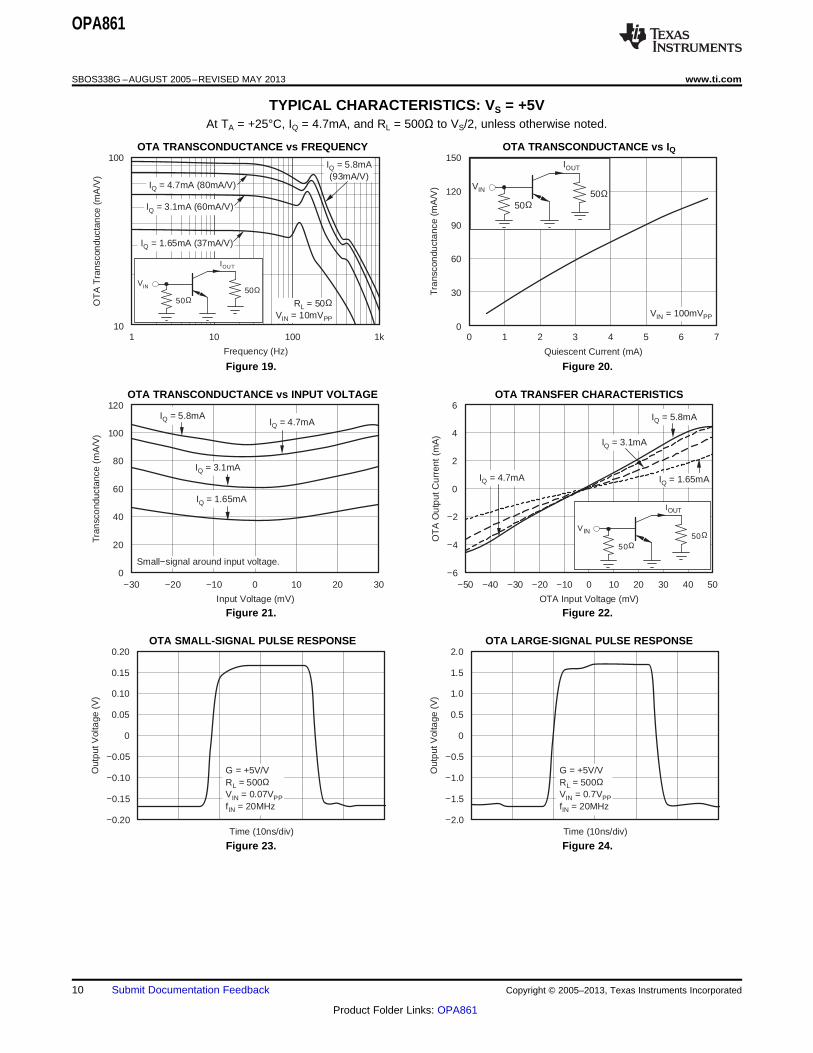
APPLICATION INFORMATION
The OPA861 is a versatile monolithic TRANSCONDUCTANCE (OTA) SECTION—ANtransconductance amplifier designed for wide- OVERVIEWbandwidth systems, including high-performancevideo, RF, and IF circuitry. The operation of the The symbol for the OTA section is similar to aOPA861 is discussed in the OTA (Operational transistor (see Figure 29). Applications circuits for theTransconductance Amplifier) section of this data OTA look and operate much like transistorsheet. Over the years and depending on the writer, circuits—the transistor is also a voltage-controlledthe OTA section of an op amp has been referred to current source. Not only does this characteristicas a Diamond Transistor, Voltage-Controlled Current simplify the understanding of application circuits, itsource, Transconductor, Macro Transistor, or positive aids the circuit optimization process as well. Many ofsecond-generation current conveyor (CCII+). the same intuitive techniques used with transistorCorresponding symbols for these terms are shown in designs apply to OTA circuits. The three terminals ofFigure 29. the OTA are labeled B, E, and C. This labeling calls
attention to its similarity to a transistor, yet drawsdistinction for clarity. While the OTA is similar to atransistor, one essential difference is the sense of theC-output current: it flows out the C terminal forpositive B-to-E input voltage and in the C terminal fornegative B-to-E input voltage. The OTA offers manyadvantages over a discrete transistor. The OTA isself-biased, simplifying the design process andreducing component count. In addition, the OTA is farmore linear than a transistor. Transconductance ofthe OTA is constant over a wide range of collectorcurrents—this feature implies a fundamentalimprovement of linearity.
BASIC CONNECTIONS
Figure 30 shows basic connections required foroperation. These connections are not shown insubsequent circuit diagrams. Power-supply bypassFigure 29. Symbols and Termscapacitors should be located as close as possible tothe device pins. Solid tantalum capacitors areRegardless of its depiction, the OTA section has agenerally best.high-input impedance (B-input), a low-input/output
impedance (E-input), and a high-impedance currentsource output (C-output).
Figure 30. Basic Connections
12 Submit Documentation Feedback Copyright © 2005–2013, Texas Instruments Incorporated
Product Folder Links: OPA861

R11.25kΩ
TLV2262
OPA8611/2 REF200100µA
R2425Ω
V+
IQ Adjust
1 I1
G RL
1gm RE
OPA861
www.ti.com SBOS338G –AUGUST 2005–REVISED MAY 2013
QUIESCENT CURRENT CONTROL PIN With this control loop, quiescent current will be nearlyconstant with temperature. Since this method differs
The quiescent current of the transconductance from the temperature-dependent behavior of theportion of the OPA861 is set with a resistor, RADJ, internal current source, other temperature-dependentconnected from pin 1 to –VS. The maximum behavior may differ from that shown in the Typicalquiescent current is 6mA. RADJ should be set Characteristics. The circuit of Figure 31 will controlbetween 50Ω and 1kΩ for optimal performance of the the IQ of the OPA861 somewhat more accurately thanOTA section. This range corresponds to the 5mA with a fixed external resistor, RQ. Otherwise, there isquiescent current for RADJ = 50Ω, and 1mA for RADJ = no fundamental advantage to using this more1kΩ. If the IQ adjust pin is connected to the negative complex biasing circuitry. It does, however,supply, the quiescent current will be set by the 250Ω demonstrate the possibility of signal-controlledinternal resistor. quiescent current. This capability may suggest other
possibilities such as AGC, dynamic control of ACReducing or increasing the quiescent current for thebehavior, or VCO.OTA section controls the bandwidth and AC behavior
as well as the transconductance. With RADJ = 250Ω,this sets approximately 5.4mA total quiescent current BASIC APPLICATIONS CIRCUITSat 25°C. It may be appropriate in some applications to
Most applications circuits for the OTA section consisttrim this resistor to achieve the desired quiescentof a few basic types, which are best understood bycurrent or AC performance.analogy to a transistor. Used in voltage-mode, the
Applications circuits generally do not show the OTA section can operate in three basic operatingresistor RQ, but it is required for proper operation. states—common emitter, common base, and
common collector. In the current-mode, the OTA canWith a fixed RADJ resistor, quiescent current be useful for analog computation such as currentincreases with temperature (see Figure 12 in the amplifier, current differentiator, current integrator, andTypical Characteristics section). This variation of current summer.current with temperature holds the transconductance,gm, of the OTA relatively constant with temperature Common-E Amplifier or Forward Amplifier(another advantage over a transistor).
Figure 32 compares the common-emitterIt is also possible to vary the quiescent current with a configuration for a BJT with the common-E amplifiercontrol signal. The control loop in Figure 31 shows for the OTA section. There are several advantages in1/2 of a REF200 current source used to develop using the OTA section in place of a BJT in this100mV on R1. The loop forces 125mV to appear on configuration. Notably, the OTA does not require anyR2. Total quiescent current of the OPA861 is biasing, and the transconductance gain remainsapproximately 37 × I1, where I1 is the current made to constant over temperature. The output offset voltageflow out of pin 1. is close to 0, compared with several volts for the
common-emitter amplifier.
The gain is set in a similar manner as for the BJTequivalent with Equation 1:
(1)
Just as transistor circuits often use emitterdegeneration, OTA circuits may also usedegeneration. This option can be used to reduce theeffects that offset voltage and offset current mightotherwise have on the DC operating point of the OTA.The E-degeneration resistor may be bypassed with alarge capacitor to maintain high AC gain. Othercircumstances may suggest a smaller value capacitorused to extend or optimize high-frequency
Figure 31. Optional Control Loop for Setting performance.Quiescent Current
Copyright © 2005–2013, Texas Instruments Incorporated Submit Documentation Feedback 13
Product Folder Links: OPA861
G =
At I = 5.4mAQ
G = at I = 5.4mAQ
VI
VO
3
2
8
RE
rE
RL2R1
100W
RIN
50W
R = R + R || RL L1 L2 IN
OTA
RL1
Network
Analyzer
RL
R + rE E
RL
R + 10.5WE
r = = 10.5WE
1
95mA/V
1
gm
r =E
gm_deg1
1gm RE
100Ω
VI
V+
V−
VI
VO
3 B
2E
C8
RS
RS
RL
RE
VO
RE
RL
Inverting GainVOS = Several Volts
Noninverting GainVOS = 0V
(a) Transistor Common−Emitter AmplifierTransconductance varies over temperature.
(b) OTA Common−E AmplifierTransconductance remains constant over temperature.
OPA861
R1160Ω
VI
VO
3 B
2E
C8
RE78Ω
RC500Ω
G = 5V/VIQ = 5.4mA
OPA861
OPA861
SBOS338G –AUGUST 2005–REVISED MAY 2013 www.ti.com
The forward amplifier shown in Figure 33 andFigure 34 corresponds to one of the basic circuitsused to characterize the OPA861. Extendedcharacterization of this topology appears in theTypical Characteristics section of this datasheet.
Figure 33. Forward Amplifier Configuration andTest Circuit
Figure 32. Common-Emitter vs Common-EAmplifier
The transconductance of the OTA with degenerationcan be calculated by Equation 2:
(2)
A positive voltage at the B-input, pin 3, causes apositive current to flow out of the C-input, pin 8. Thisgives a noninverting gain where the circuit ofFigure 32a is inverting. Figure 32b shows an amplifierconnection of the OPA861, the equivalent of acommon-emitter transistor amplifier. Input and outputcan be ground-referenced without any biasing. Theamplifier is non-inverting because of the sense of the
Figure 34. Forward Amplifier Design Equationsoutput current.
14 Submit Documentation Feedback Copyright © 2005–2013, Texas Instruments Incorporated
Product Folder Links: OPA861

G RL
RE1
gm
RL
RE
(b) OTA Common-B Amplifier
(a) Transistor Common-Base Amplifier
100W3 B
2
E
C
8
OPA861
RE
VIN
RL
Inverting Gain
V = 0VOS
VO
Noninverting Gain
V = Several VoltsOS
RE
V-
V+
RL
VO
VIN
R1
G =RL
R +E
1
gm
= -
RL
RE
G 11 1
gmRE
1
RO 1gm
RE100Ω
VI3 B
2E
C8
G = 1VOS = 0V
G = 1VOS = 0.7V
OPA861
RE
VO
(b) OTA Common−C Amplifier(Buffer)
(a) Transistor Common−Collector Amplifier(Emitter Follower)
VO
VI
RE
V−
V+
G 11 1
gmRE
1
OPA861
www.ti.com SBOS338G –AUGUST 2005–REVISED MAY 2013
Common-C Amplifier This low impedance can be converted to a highimpedance by inserting the buffer amplifier in series.Figure 35b shows the OPA861 connected as an E-
follower—a voltage buffer. It is interesting to noticeCurrent-Mode Analog Computationsthat the larger the RE resistor, the closer to unity gain
the buffer will be. If the OPA861 is to be used as a As mentioned earlier, the OPA861 can be usedbuffer, use RE ≥ 500Ω for best results. For the advantageously for analog computation. Among theOPA861 used as a buffer, the gain is given by application possibilities are functionality as a currentEquation 3: amplifier, current differentiator, current integrator,
current summer, and weighted current summer.Table 1 lists these different uses with the associated
(3) transfer functions.
These functions can easily be combined to formactive filters. Some examples using these current-mode functions are shown later in this document.
Figure 35. Common-Collector vs Common-CAmplifier
A low value resistor in series with the B-input isrecommended. This resistor helps isolate traceparasitic from the inputs, reduces any tendency tooscillate, and controls frequency response peaking.
Figure 36. Common-Base Transistor vsTypical resistor values are from 25Ω to 200Ω.Common-B OTA
Common-B Amplifier
Figure 36 shows the Common-B amplifier. Thisconfiguration produces an inverting gain and a lowimpedance input. Equation 4 shows the gain for thisconfiguration.
(4)
Copyright © 2005–2013, Texas Instruments Incorporated Submit Documentation Feedback 15
Product Folder Links: OPA861

IOUT
I1
RR1
In
RRnIOUT 1
n
j1Ij
Rj
R
IOUT
I2 InI1
IOUT 1 n
j1Ij
IOUT
IIN
C
R
IOUT 1
C R IINdt
IOUT
IIN
R1
R2IOUT
R1
R2 IIN
OPA861
SBOS338G –AUGUST 2005–REVISED MAY 2013 www.ti.com
Table 1. Current-Mode Analog Computation Using the OTA Section
FUNCTIONAL ELEMENT TRANSFER FUNCTION IMPLEMENTATION WITH THE OTA SECTION
Current Amplifier
Current Integrator
Current Summer
Weighted Current Summer
OPA861 APPLICATIONS
Control-Loop Amplifier DC-Restore Circuit
A new type of control loop amplifier for fast and The OPA861 can be used advantageously with anprecise control circuits can be designed with the operational amplifier, here the OPA656, as a DC-OPA861. The circuit of Figure 37 illustrates a series restore circuit. Figure 38 illustrates this design.connection of two voltage control current sources that Depending on the collector current of thehave an integral (and at higher frequencies, a transconductance amplifier (OTA) of the OPA861, aproportional) behavior versus frequency. The control switching function is realized with the diodes D1 andloop amplifiers show an integrator behavior from DC D2.to the frequency represented by the RC time constant
When the C-output is sourcing current, the capacitorof the network from the C-output to GND. Above thisC1 is being charged. When the C-output is sinkingfrequency, they operate as an amp with constantcurrent, D1 is turned off and D2 is turned on, lettinggain. The series connection increases the overall gainthe voltage across C1 be discharged through R2.to about 110dB and thus minimizes the control loop
deviation. The differential configuration at the inputs The condition to charge C1 is set by the voltageenables one to apply the measured output signal and difference between VREF and VOUT. For the OTA C-the reference voltage to two identical high-impedance output to source current, VREF has to be greater thaninputs. The output buffer decouples the C-output of VOUT. The rate of charge of C1 is set by both R1 andthe second OTA in order to insure the AC C1. The discharge rate is given by R2 and C1.performance and to drive subsequent output stages.
16 Submit Documentation Feedback Copyright © 2005–2013, Texas Instruments Incorporated
Product Folder Links: OPA861

C1
C2
VIN
R
R
VOUT
C C1 2
+Q =
C C1 2
0 1
C1C2 R
VOUT
VIN
1
1 + sR(C + C ) + s C C R2 1 2
2 2
1
=
20Ω
20Ω
R2100kΩ
VIN
R2100Ω
R140.2ΩCCII
B3
2EC8
VOUT
VREF
C1100pF
D1
D2
OPA656
The OTA amplifier works as a current conveyor (CCII) in this circuit, with a current gain of 1.R1 and C1 set the DC restoration time constant.
D1 adds a propagation delay to the DC restoration.R2 and C1 set the decay time constant.
D1, D2 = 1N4148RQ = 1kΩ
JFET−Input, Wideband
VOUT5
BUF6026
2
3
33Ω
10pF
10Ω
2
8
10Ω
8
33Ω
10pF
VIN
180Ω 6
VREF
180Ω
3
OPA861
www.ti.com SBOS338G –AUGUST 2005–REVISED MAY 2013
Figure 37. Control-Loop Amplifier Using Three OPA861s
Figure 38. DC Restorer Circuit
Negative Impedance Converter Filter: Low-PassThe transfer function is shown in Equation 5:Filter
The OPA861 can be used as a negative impedanceconverter to realize the low-pass filer shown in (5)Figure 39.
with:
Figure 39. Low-Pass Negative ImpedanceConverter Filter
Copyright © 2005–2013, Texas Instruments Incorporated Submit Documentation Feedback 17
Product Folder Links: OPA861

50Ω
50Ω
50Ω
50Ω
VIN
50Ω 10Ω 100Ω 10Ω
To 50ΩLoad
0
−10
−20
−30
−40
−50
−60
−70
−80
Frequency (Hz)
Gai
n(d
B)
1k 10k 100k 1M 10M 100M 1G
0
−10
−20
−30
−40
−50
−60
−70
−80
−90
−100
Frequency (MHz)
Co
mm
on−
Mod
eR
ejec
tion
Rat
io(d
Bc)
0.001 0.01 0.1 1 10 100
C112 C2 5.6F
Z IN1
2sC R 1 sRC
1 2sRC
OPA861
SBOS338G –AUGUST 2005–REVISED MAY 2013 www.ti.com
Differential Line Driver/ReceiverThe input impedance is shown in Equation 6:
The wide bandwidth and high slew rate of the(6) OPA861 current-mode amplifier make it an ideal line
driver. The circuit in Figure 42 makes use of twoFigure 40 shows the frequency responses for low-OPA861s to realize a single-ended to differentialpass, Butterworth filters set at 20kHz and 10MHz.conversion. The high-impedance current source
For the 20kHz filter, set R to 1kΩ and output of the OPA861 allows it to drive low-impedance or capacitive loads without series
. For the 10MHz filter, the resistances and avoids any attenuation that wouldparasitic capacitance at the output pin needs to be have otherwise occured in the resistive network.taken into consideration. In the example of Figure 40,
The OPA861 used as a differential receiver exhibitsthe parasitic is 3pF, which gives us the settings of Rexcellent common-mode rejection ratio, as can be= 1.13kΩ, C1 = 10pF, and C2 = 17pF.seen in Figure 41.
Figure 41. Differential Driver Common-ModeFigure 40. Small-Signal Frequency Response forRejection Ratio for 2VPP Input Signalsa Low-Pass Negative Impedance Converter Filter
Figure 42. Twisted-Pair Differential Driver and Receiver with the OPA861
18 Submit Documentation Feedback Copyright © 2005–2013, Texas Instruments Incorporated
Product Folder Links: OPA861

F(p)VOUT
VIN
s2C1C2R1M
R2MR3 sC1
R1MR2
1R1
s2C1C2R1M
R2MR3S sC1
R1MR2S
1R1S
C2 R2M
VOUT
R3
R2S
R2
R1S
C1
VIN
R1 R1M
R3S
RB1 RB2 RB3
BUF602
+
−µV µI I
C C
R R
+− VOUT
V
2
2
2
2
3
4
1
1
1
1
2
2
2
2
3
4
1
1
1
1
1
1
ControlledSources
PassiveElements
SignalSources
Element Adjoint
IOUTVIN
IIN
N VOUT
+
−
NIOUT IIN
Reciprocal Networks
N VOUT
+
−
NAIOUT IIN
Interreciprocal Networks
IINVIN
IOUTVOUT =
VIN
VIN
R
VOUT
C/2
R
+1
CVIN R
IOUT
C/2
R
CCII−
C
EB
C
IIN
VOUTT(s) = = =
IOUT
VIN IIN s2 + 2/RC[2Q(1 − K) + 1]s + 4KQ2/R2C2
4KQ2/R2C2
OPA861
www.ti.com SBOS338G –AUGUST 2005–REVISED MAY 2013
ACTIVE FILTERS USING THE OPA861 IN of the operational amplifier becomes a negativeCURRENT CONVEYOR STRUCTURE second type of Current Conveyor (CCII), as shown in
Figure 43. Both arrangements have identical transferOne further example of the versatility of the Diamond functions and the same level of sensitivity toTransistor and Buffer is the construction of high- deviations. The most recent implementation of activefrequency (> 10MHz) active filters. Here, the Current filters in a Current-Conveyor structure produced aConveyor structure, shown in Figure 43, is used with second-order Bi-Quad filter. The value of thethe Diamond Transistor as a Current Conveyor. resistance in the emitter of the Diamond Transistor
controls the filter characteristic. For more information,refer to application note SBOS047, New Ultra High-Speed Circuit Techniques with Analog ICs.
Figure 43. Current Conveyor
The method of converting RC circuit loops withoperational amplifiers in Current Conveyor structuresis based upon the adjoint network concept. A networkis reversible or reciprocal when the transfer function
Figure 44. Networksdoes not change even when the input and outputhave been exchanged. Most networks, of course, arenonreciprocal. The networks of Figure 44, performinterreciprocally when the input and output areexchanged, while the original network, N, isexchanged for a new network NA. In this case, thetransfer function remains the same, and NA is theadjoing network. It is easy to construct an adjointnetwork for any given circuit, and these networks arethe base for circuits in Current-Conveyor structure.
Figure 45. Individual Elements in the CurrentIndividual elements can be interchanged according toConveyorthe list in Figure 45. Voltage sources at the input
become short circuits, and the current flowing therebecomes the output variable. In contrast, the voltageoutput becomes the input, which is excitated by acurrent source. The following equation describes theinterreciprocal features of the circuit: VOUT/VIN =IOUT/IIN. Resistances and capacitances remainunchanged. In the final step, the operational amplifierwith infinite input impedance and 0Ω outputimpedance is transformed into a current amplifier with0Ω input impedance and infinite output impedance. ADiamond Transistor with the base at ground comesquite close to an ideal current amplifier. The well-
Figure 46. Universal Active Filterknown Sallen-Key low-pass filter with positivefeedback, is an example of conversion into Current-Conveyor structure, see Figure 46. The positive gain
Transfer Function Filter Characteristics
The transfer function of the universal active filter of Five filter types can be made with this structure:Figure 46 is shown in Equation 7. • For a low-pass filter, set R2 = R3 = ∞,
• For a high-pass filter, set R1 = R2 = ∞,• For a bandpass filter, set R1 = R3 = ∞,• For a band rejection filter, set R2 = ∞; R1 = R3,(7)• For an all-pass filter, set R1 = R1S; R2 = R2S; and
R3 = R3S.
Copyright © 2005–2013, Texas Instruments Incorporated Submit Documentation Feedback 19
Product Folder Links: OPA861

6
3
0
−3
−6
−9
Frequency (Hz)
Gai
n(d
B)
1M 10M 100M 1G
5.6dB
600Ω
600Ω
VIN1
VCM
VIN2
RE600Ω
ADS5272OPA861
OPA861
30
-3-6-9
-12-15-18-21-24-27-30-33-36-39-42-45-48
Frequency (Hz)
Gain
(dB
)
10k 100k 1M 10M 100M 1G
50MHz Filter
20MHz Filter
1MHz Filter
For All Filters:
R = R =2 ¥3
R = R = R1 1S 2S 3S= 1/2 R = R
R = R = R1M 2M 0
C = C = C1 2 0
OPA861
SBOS338G –AUGUST 2005–REVISED MAY 2013 www.ti.com
A few designs for a low-pass filter are shown in High-CMRR, Moderate Precision, DifferentialFigure 47 and Table 2. I/O ADC Driver
The circuit shown in Figure 48 depicts an ADC driverTable 2. Component Values for Filters Shown Inimplemented with two OPA861s. Since the gain is setFigure 47here by the ratio of the internal 600Ω resistors and
fO R RO CO RE, its accuracy will only be as good as the input1MHz 150 100 2nF resistor of the ADS5272. The small-signal frequency
response for this circuit has 150MHz at –3dB20MHz 150 100 112.5pFbandwidth for a gain of approximately 5.6dB, as50MHz 150 100 25pFshown in Figure 49. The advantage of this circuit liesin its high CMRR to 100kHz; see Figure 50. Thiscircuit also has more than 10 bits of linearity.
Figure 47. Butterworth Low-Pass Filter with theUniversal Active Filter Figure 48. High CMRR, Moderate Precision,
Differential I/O ADC DriverThe advantages of building active filters using aCurrent Conveyor structure are:• The increase in output resistance of operational
amplifiers at high frequencies makes it difficult toconstruct feedback filter structures (decrease instop-band attenuation).
• All filter coefficients are represented byresistances, making it possible to adjust the filterfrequency response without affecting the filtercoefficients.
• The capacitors which determine the frequency arelocated between the ground and the currentsource outputs and are thus grounded on oneside. Therefore, all parasitic capacitances can beviewed as part of these capacitors, making themeasier to comprehend.
• The features which determine the frequencyFigure 49. ADC Driver, Small-Signal Frequencycharacteristics are currents, which charge the
Responseintegration capacitors. This situation is similar tothe transfer characteristic of the DiamondTransistor.
20 Submit Documentation Feedback Copyright © 2005–2013, Texas Instruments Incorporated
Product Folder Links: OPA861

e =O[e + (R i ) + 4kTR + (R i ) + 4kTR ]N S BN G BIS G
2 2 2
2RL
RG +1
gm
en
ibn ibi
RS RG
√4kTRS √4kTRS
RL
VO
75
70
65
60
55
50
45
40
35
30
25
20
Frequency (Hz)
Com
mon
−M
ode
Rej
ectio
nR
atio
(dB
)
1k 10k 100k 1M 10M 100M 1G
Input−Referred
OPA861
www.ti.com SBOS338G –AUGUST 2005–REVISED MAY 2013
NOISE PERFORMANCE
The OTA noise model consists of three elements: avoltage noise on the B-input; a current noise on theB-input; and a current noise on the E-input. Figure 51shows the OTA noise analysis model with all thenoise terms included. In this model, all noise termsare taken to be noise voltage or current density termsin either nV/√Hz or pA/√Hz.
Figure 50. CMRR of the ADC Driver
DESIGN-IN TOOLSFigure 51. OTA Noise Analysis Model
DEMONSTRATION BOARDSThe total output spot noise voltage can be computedA printed circuit board (PCB) is available to assist in as the square root of the sum of all squared outputthe initial evaluation of circuit performance using the noise voltage contributors. Equation 8 shows theOPA861. This module is available free, as an general form for the output noise voltage using theunpopulated PCB delivered with descriptive terms shown in Figure 51.documentation. The summary information for the
board is shown below:
LITERATUREBOARD PART REQUEST
PRODUCT PACKAGE NUMBER NUMBER(8)
OPA861ID SO-8 DEM-OTA-SO-1A SBOU035
THERMAL ANALYSISThe board can be requested on the TexasInstruments web site (www.ti.com). Maximum desired junction temperature will set the
maximum allowed internal power dissipation asMACROMODELS AND APPLICATIONS described below. In no case should the maximumSUPPORT junction temperature be allowed to exceed 150°C.
Computer simulation of circuit performance using Operating junction temperature (TJ) is given bySPICE is often useful when analyzing the TA + PD × θ JA. The total internal power dissipationperformance of analog circuits and systems. This (PD) is the sum of quiescent power (PDQ) andprinciple is particularly true for Video and RF amplifier additional power dissipated in the output stage (PDL)circuits where parasitic capacitance and inductance to deliver output current. Quiescent power is simplycan have a major effect on circuit performance. A the specified no-load supply current times the totalSPICE model for the OPA861 is available through the supply voltage across the part. PDL will depend on theTexas Instruments web page (www.ti.com). These required output signal and load but would, for themodels do a good job of predicting small-signal AC OPA861 be at a maximum when the maximum IO isand transient performance under a wide variety of being driven into a voltage source that puts theoperating conditions. They do not do as well in maximum voltage across the output stage. Maximumpredicting the harmonic distortion. These models do IO is 15mA times a 9V maximum across the output.not attempt to distinguish between the package types
Note that it is the power in the output stage and notin their small-signal AC performance.into the load that determines internal powerdissipation.
Copyright © 2005–2013, Texas Instruments Incorporated Submit Documentation Feedback 21
Product Folder Links: OPA861

ExternalPin
+VCC
−VCC
InternalCircuitry
OPA861
SBOS338G –AUGUST 2005–REVISED MAY 2013 www.ti.com
As a worst-case example, compute the maximum TJ c) Careful selection and placement of externalusing an OPA861IDBV in the circuit of Figure 32b components will preserve the high-frequencyoperating at the maximum specified ambient performance of the OPA861. Resistors should be atemperature of +85°C and driving a –1V voltage very low reactance type. Surface-mount resistorsreference. work best and allow a tighter overall layout. Metal film
or carbon composition, axially-leaded resistors canPD = 10V × 5.4mA + (15mA × 9V) = 185mW also provide good high-frequency performance.
Again, keep their leads and PC board traces as shortMaximum TJ = +85°C + (0.19W × 150°C/W) = 114°C.as possible. Never use wirewound type resistors in a
Although this is still well below the specified high-frequency application.maximum junction temperature, system reliability
d) Connections to other wideband devices on theconsiderations may require lower tested junctionboard may be made with short, direct traces ortemperatures. The highest possible internalthrough onboard transmission lines. For shortdissipation will occur if the load requires current to beconnections, consider the trace and the input to theforced into the output for positive output voltages ornext device as a lumped capacitive load. Relativelysourced from the output for negative output voltages.wide traces (50mils to 100mils) should be used,This puts a high current through a large internalpreferably with ground and power planes opened upvoltage drop in the output transistors.around them.
BOARD LAYOUT GUIDELINES e) Socketing a high-speed part like the OPA861 isnot recommended. The additional lead length and
Achieving optimum performance with a high- pin-to-pin capacitance introduced by the socket canfrequency amplifier like the OPA861 requires careful create an extremely troublesome parasitic networkattention to board layout parasitics and external that makes it almost impossible to achieve a smooth,component types. Recommendations that will stable frequency response. Best results are obtainedoptimize performance include: by soldering the OPA861 onto the board.a) Minimize parasitic capacitance to any AC ground
INPUT AND ESD PROTECTIONfor all of the signal I/O pins. Parasitic capacitance onthe inverting input pin can cause instability: on the The OPA861 is built using a very high-speednoninverting input, it can react with the source complementary bipolar process. The internal junctionimpedance to cause unintentional bandlimiting. To breakdown voltages are relatively low for these veryreduce unwanted capacitance, a window around the small geometry devices. These breakdowns aresignal I/O pins should be opened in all of the ground reflected in the Absolute Maximum Ratings table. Alland power planes around those pins. Otherwise, device pins are protected with internal ESD protectionground and power planes should be unbroken diodes to the power supplies as shown in Figure 52.elsewhere on the board.
b) Minimize the distance (< 0.25") from the power-supply pins to high-frequency 0.1µF decouplingcapacitors. At the device pins, the ground and power-plane layout should not be in close proximity to thesignal I/O pins. Avoid narrow power and groundtraces to minimize inductance between the pins andthe decoupling capacitors. The power-supplyconnections should always be decoupled with thesecapacitors. An optional supply decoupling capacitor
Figure 52. Internal ESD Protection(0.1µF) across the two power supplies (for bipolaroperation) will improve 2nd-harmonic distortionperformance. Larger (2.2µF to 6.8µF) decoupling These diodes provide moderate protection to inputcapacitors, effective at lower frequency, should also overdrive voltages above the supplies as well. Thebe used on the main supply pins. These may be protection diodes can typically support 30mAplaced somewhat farther from the device and may be continuous current. Where higher currents areshared among several devices in the same area of possible (for example, in systems with ±15V supplythe PC board. parts driving into the OPA861), current-limiting series
resistors should be added into the two inputs. Keepthese resistor values as low as possible since highvalues degrade both noise performance andfrequency response.
22 Submit Documentation Feedback Copyright © 2005–2013, Texas Instruments Incorporated
Product Folder Links: OPA861

OPA861
www.ti.com SBOS338G –AUGUST 2005–REVISED MAY 2013
REVISION HISTORY
NOTE: Page numbers for previous revisions may differ from page numbers in the current version.
Changes from Revision F (May 2011) to Revision G Page
• Changed transfer function equations in Negative Impedance Converter Filter: Low-Pass Filter section .......................... 17
Changes from Revision E (August 2008) to Revision F Page
• Updated Figure 30 .............................................................................................................................................................. 12
• Updated Equation 8 ............................................................................................................................................................ 21
Changes from Revision D (August 2006) to Revision E Page
• Changed storage temperature range rating in Absolute Maximum Ratings table from –40°C to +125°C to –65°C to+125°C .................................................................................................................................................................................. 2
Copyright © 2005–2013, Texas Instruments Incorporated Submit Documentation Feedback 23
Product Folder Links: OPA861

PACKAGE OPTION ADDENDUM
www.ti.com 17-Mar-2017
Addendum-Page 1
PACKAGING INFORMATION
Orderable Device Status(1)
Package Type PackageDrawing
Pins PackageQty
Eco Plan(2)
Lead/Ball Finish(6)
MSL Peak Temp(3)
Op Temp (°C) Device Marking(4/5)
Samples
OPA861ID ACTIVE SOIC D 8 75 Green (RoHS& no Sb/Br)
CU NIPDAU Level-2-260C-1 YEAR -40 to 85 OPA861
OPA861IDBVT ACTIVE SOT-23 DBV 6 250 Green (RoHS& no Sb/Br)
CU NIPDAU Level-2-260C-1 YEAR -40 to 85 NSR
OPA861IDBVTG4 ACTIVE SOT-23 DBV 6 250 Green (RoHS& no Sb/Br)
CU NIPDAU Level-2-260C-1 YEAR -40 to 85 NSR
OPA861IDG4 ACTIVE SOIC D 8 75 Green (RoHS& no Sb/Br)
CU NIPDAU Level-2-260C-1 YEAR -40 to 85 OPA861
(1) The marketing status values are defined as follows:ACTIVE: Product device recommended for new designs.LIFEBUY: TI has announced that the device will be discontinued, and a lifetime-buy period is in effect.NRND: Not recommended for new designs. Device is in production to support existing customers, but TI does not recommend using this part in a new design.PREVIEW: Device has been announced but is not in production. Samples may or may not be available.OBSOLETE: TI has discontinued the production of the device.
(2) Eco Plan - The planned eco-friendly classification: Pb-Free (RoHS), Pb-Free (RoHS Exempt), or Green (RoHS & no Sb/Br) - please check http://www.ti.com/productcontent for the latest availabilityinformation and additional product content details.TBD: The Pb-Free/Green conversion plan has not been defined.Pb-Free (RoHS): TI's terms "Lead-Free" or "Pb-Free" mean semiconductor products that are compatible with the current RoHS requirements for all 6 substances, including the requirement thatlead not exceed 0.1% by weight in homogeneous materials. Where designed to be soldered at high temperatures, TI Pb-Free products are suitable for use in specified lead-free processes.Pb-Free (RoHS Exempt): This component has a RoHS exemption for either 1) lead-based flip-chip solder bumps used between the die and package, or 2) lead-based die adhesive used betweenthe die and leadframe. The component is otherwise considered Pb-Free (RoHS compatible) as defined above.Green (RoHS & no Sb/Br): TI defines "Green" to mean Pb-Free (RoHS compatible), and free of Bromine (Br) and Antimony (Sb) based flame retardants (Br or Sb do not exceed 0.1% by weightin homogeneous material)
(3) MSL, Peak Temp. - The Moisture Sensitivity Level rating according to the JEDEC industry standard classifications, and peak solder temperature.
(4) There may be additional marking, which relates to the logo, the lot trace code information, or the environmental category on the device.
(5) Multiple Device Markings will be inside parentheses. Only one Device Marking contained in parentheses and separated by a "~" will appear on a device. If a line is indented then it is a continuationof the previous line and the two combined represent the entire Device Marking for that device.
(6) Lead/Ball Finish - Orderable Devices may have multiple material finish options. Finish options are separated by a vertical ruled line. Lead/Ball Finish values may wrap to two lines if the finishvalue exceeds the maximum column width.

PACKAGE OPTION ADDENDUM
www.ti.com 17-Mar-2017
Addendum-Page 2
Important Information and Disclaimer:The information provided on this page represents TI's knowledge and belief as of the date that it is provided. TI bases its knowledge and belief on informationprovided by third parties, and makes no representation or warranty as to the accuracy of such information. Efforts are underway to better integrate information from third parties. TI has taken andcontinues to take reasonable steps to provide representative and accurate information but may not have conducted destructive testing or chemical analysis on incoming materials and chemicals.TI and TI suppliers consider certain information to be proprietary, and thus CAS numbers and other limited information may not be available for release.
In no event shall TI's liability arising out of such information exceed the total purchase price of the TI part(s) at issue in this document sold by TI to Customer on an annual basis.


IMPORTANT NOTICE
Texas Instruments Incorporated (TI) reserves the right to make corrections, enhancements, improvements and other changes to itssemiconductor products and services per JESD46, latest issue, and to discontinue any product or service per JESD48, latest issue. Buyersshould obtain the latest relevant information before placing orders and should verify that such information is current and complete.TI’s published terms of sale for semiconductor products (http://www.ti.com/sc/docs/stdterms.htm) apply to the sale of packaged integratedcircuit products that TI has qualified and released to market. Additional terms may apply to the use or sale of other types of TI products andservices.Reproduction of significant portions of TI information in TI data sheets is permissible only if reproduction is without alteration and isaccompanied by all associated warranties, conditions, limitations, and notices. TI is not responsible or liable for such reproduceddocumentation. Information of third parties may be subject to additional restrictions. Resale of TI products or services with statementsdifferent from or beyond the parameters stated by TI for that product or service voids all express and any implied warranties for theassociated TI product or service and is an unfair and deceptive business practice. TI is not responsible or liable for any such statements.Buyers and others who are developing systems that incorporate TI products (collectively, “Designers”) understand and agree that Designersremain responsible for using their independent analysis, evaluation and judgment in designing their applications and that Designers havefull and exclusive responsibility to assure the safety of Designers' applications and compliance of their applications (and of all TI productsused in or for Designers’ applications) with all applicable regulations, laws and other applicable requirements. Designer represents that, withrespect to their applications, Designer has all the necessary expertise to create and implement safeguards that (1) anticipate dangerousconsequences of failures, (2) monitor failures and their consequences, and (3) lessen the likelihood of failures that might cause harm andtake appropriate actions. Designer agrees that prior to using or distributing any applications that include TI products, Designer willthoroughly test such applications and the functionality of such TI products as used in such applications.TI’s provision of technical, application or other design advice, quality characterization, reliability data or other services or information,including, but not limited to, reference designs and materials relating to evaluation modules, (collectively, “TI Resources”) are intended toassist designers who are developing applications that incorporate TI products; by downloading, accessing or using TI Resources in anyway, Designer (individually or, if Designer is acting on behalf of a company, Designer’s company) agrees to use any particular TI Resourcesolely for this purpose and subject to the terms of this Notice.TI’s provision of TI Resources does not expand or otherwise alter TI’s applicable published warranties or warranty disclaimers for TIproducts, and no additional obligations or liabilities arise from TI providing such TI Resources. TI reserves the right to make corrections,enhancements, improvements and other changes to its TI Resources. TI has not conducted any testing other than that specificallydescribed in the published documentation for a particular TI Resource.Designer is authorized to use, copy and modify any individual TI Resource only in connection with the development of applications thatinclude the TI product(s) identified in such TI Resource. NO OTHER LICENSE, EXPRESS OR IMPLIED, BY ESTOPPEL OR OTHERWISETO ANY OTHER TI INTELLECTUAL PROPERTY RIGHT, AND NO LICENSE TO ANY TECHNOLOGY OR INTELLECTUAL PROPERTYRIGHT OF TI OR ANY THIRD PARTY IS GRANTED HEREIN, including but not limited to any patent right, copyright, mask work right, orother intellectual property right relating to any combination, machine, or process in which TI products or services are used. Informationregarding or referencing third-party products or services does not constitute a license to use such products or services, or a warranty orendorsement thereof. Use of TI Resources may require a license from a third party under the patents or other intellectual property of thethird party, or a license from TI under the patents or other intellectual property of TI.TI RESOURCES ARE PROVIDED “AS IS” AND WITH ALL FAULTS. TI DISCLAIMS ALL OTHER WARRANTIES ORREPRESENTATIONS, EXPRESS OR IMPLIED, REGARDING RESOURCES OR USE THEREOF, INCLUDING BUT NOT LIMITED TOACCURACY OR COMPLETENESS, TITLE, ANY EPIDEMIC FAILURE WARRANTY AND ANY IMPLIED WARRANTIES OFMERCHANTABILITY, FITNESS FOR A PARTICULAR PURPOSE, AND NON-INFRINGEMENT OF ANY THIRD PARTY INTELLECTUALPROPERTY RIGHTS. TI SHALL NOT BE LIABLE FOR AND SHALL NOT DEFEND OR INDEMNIFY DESIGNER AGAINST ANY CLAIM,INCLUDING BUT NOT LIMITED TO ANY INFRINGEMENT CLAIM THAT RELATES TO OR IS BASED ON ANY COMBINATION OFPRODUCTS EVEN IF DESCRIBED IN TI RESOURCES OR OTHERWISE. IN NO EVENT SHALL TI BE LIABLE FOR ANY ACTUAL,DIRECT, SPECIAL, COLLATERAL, INDIRECT, PUNITIVE, INCIDENTAL, CONSEQUENTIAL OR EXEMPLARY DAMAGES INCONNECTION WITH OR ARISING OUT OF TI RESOURCES OR USE THEREOF, AND REGARDLESS OF WHETHER TI HAS BEENADVISED OF THE POSSIBILITY OF SUCH DAMAGES.Unless TI has explicitly designated an individual product as meeting the requirements of a particular industry standard (e.g., ISO/TS 16949and ISO 26262), TI is not responsible for any failure to meet such industry standard requirements.Where TI specifically promotes products as facilitating functional safety or as compliant with industry functional safety standards, suchproducts are intended to help enable customers to design and create their own applications that meet applicable functional safety standardsand requirements. Using products in an application does not by itself establish any safety features in the application. Designers mustensure compliance with safety-related requirements and standards applicable to their applications. Designer may not use any TI products inlife-critical medical equipment unless authorized officers of the parties have executed a special contract specifically governing such use.Life-critical medical equipment is medical equipment where failure of such equipment would cause serious bodily injury or death (e.g., lifesupport, pacemakers, defibrillators, heart pumps, neurostimulators, and implantables). Such equipment includes, without limitation, allmedical devices identified by the U.S. Food and Drug Administration as Class III devices and equivalent classifications outside the U.S.TI may expressly designate certain products as completing a particular qualification (e.g., Q100, Military Grade, or Enhanced Product).Designers agree that it has the necessary expertise to select the product with the appropriate qualification designation for their applicationsand that proper product selection is at Designers’ own risk. Designers are solely responsible for compliance with all legal and regulatoryrequirements in connection with such selection.Designer will fully indemnify TI and its representatives against any damages, costs, losses, and/or liabilities arising out of Designer’s non-compliance with the terms and provisions of this Notice.
Mailing Address: Texas Instruments, Post Office Box 655303, Dallas, Texas 75265Copyright © 2018, Texas Instruments Incorporated


![130316 tsubo v1.ppt [互換モード] - JST · 2017. 12. 27. · 2 802.20 802.11ac LTE LTE-A 10k 100k 1M 10M 10m 100m 1000m Bluetooth 802.15.1 PHS PDC W-CDMA cdma2000 802.11 802.11a/g](https://img.pdfslide.net/doc/110x75/606668cd23781d49b0398c2e/130316-tsubo-v1ppt-fff-jst-2017-12-27-2-80220-80211ac-lte.jpg)