Embed Size (px)
Citation preview

www.ti.com
FEATURES APPLICATIONS
DESCRIPTION
75
80
85
90
10 20 30 40 50
dB
f − Frequency − MHz
Combined THS4304 andADS5500 SFDR
G = 10 dB,RF = 249 Ω,RG = 115 Ω,SNR = 69.6,FS = 125 MSPS
+5V
AIN+
A IN−
ADS 5500
RFRG
49.9
VIN
From50−Ωsource
1001:1
RFRG
CM
CM
0.1
THS 4304
THS 4304
1k
+3.3 VA +3.3 VD
D
A
0.1
+5V
10 k
VREF (= 2.5V)
VREF
VREF
VREF
1nF
1nF
+5VCMΩ
Ω
100Ω
Ω
10 kΩ
Ω
1k Ω
µF
µF
THS4304
SLOS436A–MARCH 2004–REVISED JULY 2004
Wideband Operational Amplifier
• Active Filter• Wide Bandwidth: 3 GHz• ADC Driver• High Slew Rate: 830 V/µs• Ultrasound• Low Voltage Noise: 2.4 nV/√Hz• Gamma Camera• Single Supply: 5 V, 3 V• RF/Telecom• Quiescent Current: 18 mA
The THS4304 is a wideband, voltage-feedback operational amplifier designed for use in high-speed analogsignal-processing chains operating with a single 5-V power supply. Developed in the BiCom3 silicon germaniumprocess technology, the THS4304 offers best-in-class performance using a single 5-V supply as opposed toprevious generations of operational amplifiers requiring ±5-V supplies.
The THS4304 is a traditional voltage-feedback topology that provides the following benefits: balanced inputs, lowoffset voltage and offset current, low offset drift, high common mode and power supply rejection ratio.
The THS4304 is offered in 8-pin MSOP package (DGK), the 8-pin SOIC package (D), and the space-saving 5-pinSOT-23 package (DBV).
DIFFERENTIAL ADC DRIVE
Please be aware that an important notice concerning availability, standard warranty, and use in critical applications of TexasInstruments semiconductor products and disclaimers thereto appears at the end of this data sheet.
PRODUCTION DATA information is current as of publication date. Copyright © 2004, Texas Instruments IncorporatedProducts conform to specifications per the terms of the TexasInstruments standard warranty. Production processing does notnecessarily include testing of all parameters.
www.ti.com
1
2
3
4 5
8
7
6
1
2
3
5
4
VOUT
VS−
IN+
VS+
IN−IN+
IN−
NC
VS−
NC
VS+
VOUT
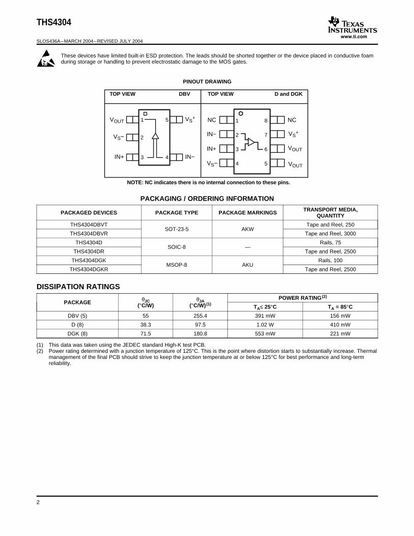
TOP VIEW TOP VIEWDBV D and DGK
NOTE: NC indicates there is no internal connection to these pins.
VOUT
DISSIPATION RATINGS
THS4304
SLOS436A–MARCH 2004–REVISED JULY 2004
These devices have limited built-in ESD protection. The leads should be shorted together or the device placed in conductive foamduring storage or handling to prevent electrostatic damage to the MOS gates.
PINOUT DRAWING
PACKAGING / ORDERING INFORMATION
TRANSPORT MEDIA,PACKAGED DEVICES PACKAGE TYPE PACKAGE MARKINGS QUANTITY
THS4304DBVT Tape and Reel, 250SOT-23-5 AKW
THS4304DBVR Tape and Reel, 3000
THS4304D Rails, 75SOIC-8 —
THS4304DR Tape and Reel, 2500
THS4304DGK Rails, 100MSOP-8 AKU
THS4304DGKR Tape and Reel, 2500
POWER RATING (2)θJC θJAPACKAGE (°C/W) (°C/W) (1)TA≤ 25°C TA = 85°C
DBV (5) 55 255.4 391 mW 156 mW
D (8) 38.3 97.5 1.02 W 410 mW
DGK (8) 71.5 180.8 553 mW 221 mW
(1) This data was taken using the JEDEC standard High-K test PCB.(2) Power rating determined with a junction temperature of 125°C. This is the point where distortion starts to substantially increase. Thermal
management of the final PCB should strive to keep the junction temperature at or below 125°C for best performance and long-termreliability.
2
www.ti.com
ABSOLUTE MAXIMUM RATINGS (1)
RECOMMENDED OPERATING CONDITIONS
THS4304
SLOS436A–MARCH 2004–REVISED JULY 2004
over operating free-air temperature range (unless otherwise noted)
UNIT
VS Supply voltage +6.0 V
VI Input voltage ±VS
IO Output current 150 mA
VID Differential input voltage ±2 V
Continuous power dissipation See Dissipation Rating Table
Maximum junction temperature, any condition (2) 150°CTJ Operating free-air temperature range, continuous operation, long-term reliability (2) 125°C
Tstg Storage temperature range –65°C to 150°C
Lead temperature: 1,6 mm (1/16 inch) from case for 10 seconds 300°C
HBM 1600 V
ESD Ratings CDM 1000 V
MM 100 V
(1) The absolute maximum ratings under any condition is limited by the constraints of the silicon process. Stresses above these ratings maycause permanent damage. Exposure to absolute maximum conditions for extended periods may degrade device reliability. These arestress ratings only, and functional operation of the device at these or any other conditions beyond those specified is not implied.
(2) The maximum junction temperature for continuous operation is limited by package constraints. Operation above this temperature mayresult in reduced reliability and/or lifetime of the device.
over operating free-air temperature range (unless otherwise noted)
MIN MAX UNIT
Dual supply ±1.35 ±2.5Supply voltage, (VS+ and VS–) V
Single supply 2.7 5
Input common-mode voltage range VS–– 0.2 VS+ + 0.2 V
3
www.ti.com
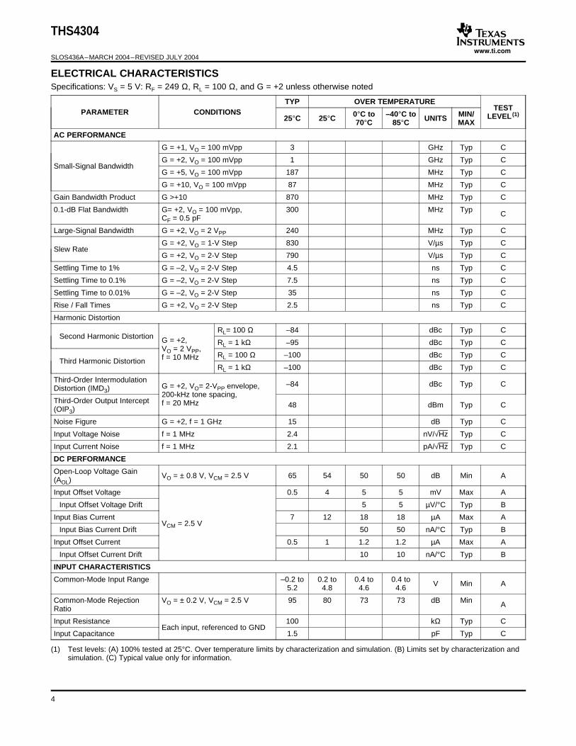
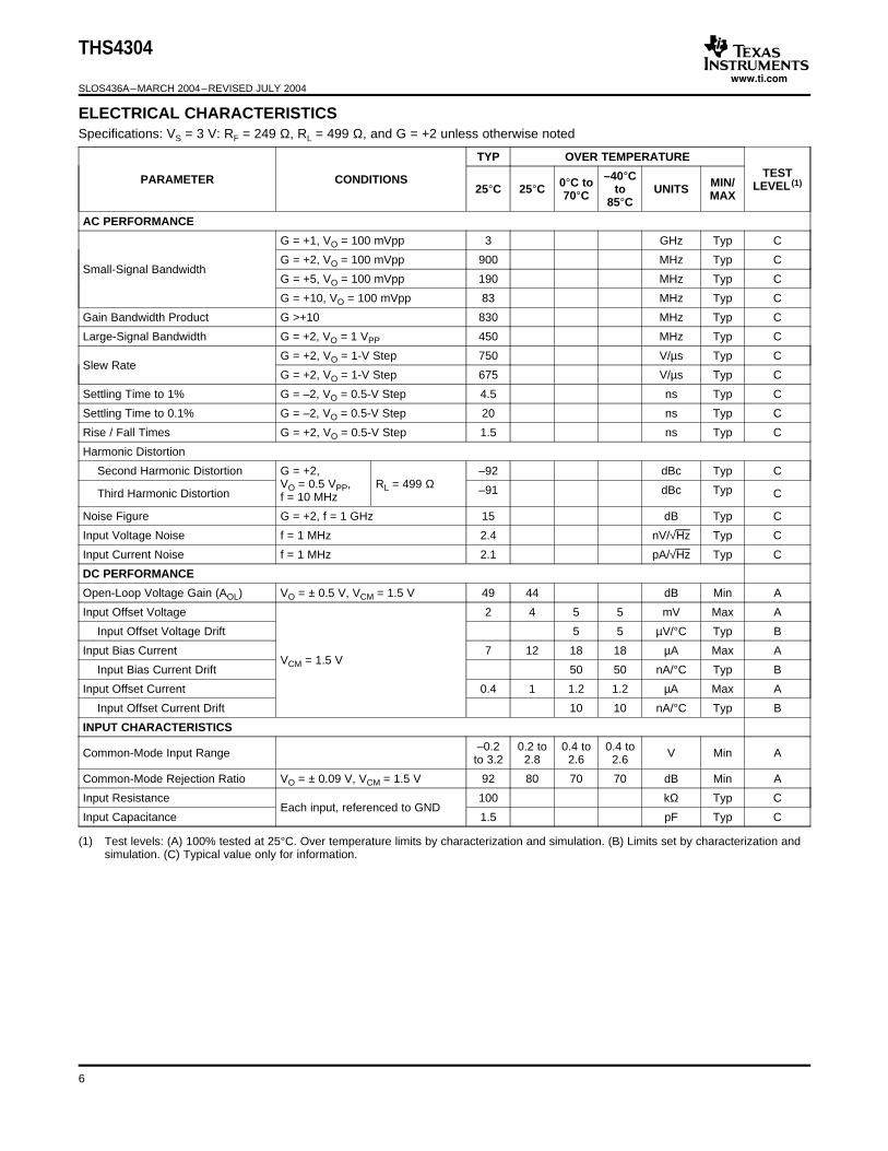
ELECTRICAL CHARACTERISTICS
THS4304
SLOS436A–MARCH 2004–REVISED JULY 2004
Specifications: VS = 5 V: RF = 249 Ω, RL = 100 Ω, and G = +2 unless otherwise noted
TYP OVER TEMPERATURETESTPARAMETER CONDITIONS 0°C to –40°C to MIN/ LEVEL (1)
25°C 25°C UNITS70°C 85°C MAX
AC PERFORMANCE
G = +1, VO = 100 mVpp 3 GHz Typ C
G = +2, VO = 100 mVpp 1 GHz Typ CSmall-Signal Bandwidth
G = +5, VO = 100 mVpp 187 MHz Typ C
G = +10, VO = 100 mVpp 87 MHz Typ C
Gain Bandwidth Product G >+10 870 MHz Typ C
0.1-dB Flat Bandwidth G= +2, VO = 100 mVpp, 300 MHz Typ CCF = 0.5 pF
Large-Signal Bandwidth G = +2, VO = 2 VPP 240 MHz Typ C
G = +2, VO = 1-V Step 830 V/µs Typ CSlew Rate
G = +2, VO = 2-V Step 790 V/µs Typ C
Settling Time to 1% G = –2, VO = 2-V Step 4.5 ns Typ C
Settling Time to 0.1% G = –2, VO = 2-V Step 7.5 ns Typ C
Settling Time to 0.01% G = –2, VO = 2-V Step 35 ns Typ C
Rise / Fall Times G = +2, VO = 2-V Step 2.5 ns Typ C
Harmonic Distortion
RL= 100 Ω –84 dBc Typ CSecond Harmonic Distortion G = +2, RL = 1 kΩ –95 dBc Typ C
VO = 2 VPP,RL = 100 Ω –100 dBc Typ Cf = 10 MHzThird Harmonic DistortionRL = 1 kΩ –100 dBc Typ C
Third-Order Intermodulation –84 dBc Typ CG = +2, VO= 2-VPP envelope,Distortion (IMD3)200-kHz tone spacing,
Third-Order Output Intercept f = 20 MHz 48 dBm Typ C(OIP3)
Noise Figure G = +2, f = 1 GHz 15 dB Typ C
Input Voltage Noise f = 1 MHz 2.4 nV/√Hz Typ C
Input Current Noise f = 1 MHz 2.1 pA/√Hz Typ C
DC PERFORMANCE
Open-Loop Voltage Gain VO = ± 0.8 V, VCM = 2.5 V 65 54 50 50 dB Min A(AOL)
Input Offset Voltage 0.5 4 5 5 mV Max A
Input Offset Voltage Drift 5 5 µV/°C Typ B
Input Bias Current 7 12 18 18 µA Max AVCM = 2.5 V
Input Bias Current Drift 50 50 nA/°C Typ B
Input Offset Current 0.5 1 1.2 1.2 µA Max A
Input Offset Current Drift 10 10 nA/°C Typ B
INPUT CHARACTERISTICS
Common-Mode Input Range –0.2 to 0.2 to 0.4 to 0.4 to V Min A5.2 4.8 4.6 4.6
Common-Mode Rejection VO = ± 0.2 V, VCM = 2.5 V 95 80 73 73 dB Min ARatio
Input Resistance 100 kΩ Typ CEach input, referenced to GND
Input Capacitance 1.5 pF Typ C
(1) Test levels: (A) 100% tested at 25°C. Over temperature limits by characterization and simulation. (B) Limits set by characterization andsimulation. (C) Typical value only for information.
4
www.ti.com
THS4304
SLOS436A–MARCH 2004–REVISED JULY 2004
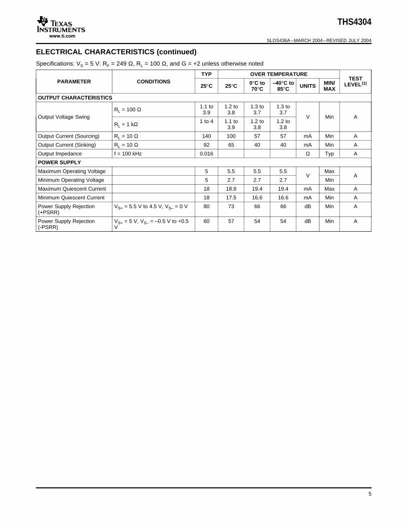
ELECTRICAL CHARACTERISTICS (continued)
Specifications: VS = 5 V: RF = 249 Ω, RL = 100 Ω, and G = +2 unless otherwise noted
TYP OVER TEMPERATURETESTPARAMETER CONDITIONS 0°C to –40°C to MIN/ LEVEL (1)
25°C 25°C UNITS70°C 85°C MAX
OUTPUT CHARACTERISTICS
1.1 to 1.2 to 1.3 to 1.3 toRL = 100 Ω 3.9 3.8 3.7 3.7Output Voltage Swing V Min A
1 to 4 1.1 to 1.2 to 1.2 toRL = 1 kΩ 3.9 3.8 3.8
Output Current (Sourcing) RL = 10 Ω 140 100 57 57 mA Min A
Output Current (Sinking) RL = 10 Ω 92 65 40 40 mA Min A
Output Impedance f = 100 kHz 0.016 Ω Typ A
POWER SUPPLY
Maximum Operating Voltage 5 5.5 5.5 5.5 MaxV A
Minimum Operating Voltage 5 2.7 2.7 2.7 Min
Maximum Quiescent Current 18 18.9 19.4 19.4 mA Max A
Minimum Quiescent Current 18 17.5 16.6 16.6 mA Min A
Power Supply Rejection VS+ = 5.5 V to 4.5 V, VS– = 0 V 80 73 66 66 dB Min A(+PSRR)
Power Supply Rejection VS+ = 5 V, VS– = –0.5 V to +0.5 60 57 54 54 dB Min A(-PSRR) V
5
www.ti.com
ELECTRICAL CHARACTERISTICS
THS4304
SLOS436A–MARCH 2004–REVISED JULY 2004
Specifications: VS = 3 V: RF = 249 Ω, RL = 499 Ω, and G = +2 unless otherwise noted
TYP OVER TEMPERATURETEST–40°CPARAMETER CONDITIONS 0°C to MIN/ LEVEL (1)
25°C 25°C to UNITS70°C MAX85°C
AC PERFORMANCE
G = +1, VO = 100 mVpp 3 GHz Typ C
G = +2, VO = 100 mVpp 900 MHz Typ CSmall-Signal Bandwidth
G = +5, VO = 100 mVpp 190 MHz Typ C
G = +10, VO = 100 mVpp 83 MHz Typ C
Gain Bandwidth Product G >+10 830 MHz Typ C
Large-Signal Bandwidth G = +2, VO = 1 VPP 450 MHz Typ C
G = +2, VO = 1-V Step 750 V/µs Typ CSlew Rate
G = +2, VO = 1-V Step 675 V/µs Typ C
Settling Time to 1% G = –2, VO = 0.5-V Step 4.5 ns Typ C
Settling Time to 0.1% G = –2, VO = 0.5-V Step 20 ns Typ C
Rise / Fall Times G = +2, VO = 0.5-V Step 1.5 ns Typ C
Harmonic Distortion
Second Harmonic Distortion G = +2, –92 dBc Typ CVO = 0.5 VPP, RL = 499 Ω –91 dBc TypThird Harmonic Distortion Cf = 10 MHz
Noise Figure G = +2, f = 1 GHz 15 dB Typ C
Input Voltage Noise f = 1 MHz 2.4 nV/√Hz Typ C
Input Current Noise f = 1 MHz 2.1 pA/√Hz Typ C
DC PERFORMANCE
Open-Loop Voltage Gain (AOL) VO = ± 0.5 V, VCM = 1.5 V 49 44 dB Min A
Input Offset Voltage 2 4 5 5 mV Max A
Input Offset Voltage Drift 5 5 µV/°C Typ B
Input Bias Current 7 12 18 18 µA Max AVCM = 1.5 V
Input Bias Current Drift 50 50 nA/°C Typ B
Input Offset Current 0.4 1 1.2 1.2 µA Max A
Input Offset Current Drift 10 10 nA/°C Typ B
INPUT CHARACTERISTICS
–0.2 0.2 to 0.4 to 0.4 toCommon-Mode Input Range V Min Ato 3.2 2.8 2.6 2.6
Common-Mode Rejection Ratio VO = ± 0.09 V, VCM = 1.5 V 92 80 70 70 dB Min A
Input Resistance 100 kΩ Typ CEach input, referenced to GND
Input Capacitance 1.5 pF Typ C
(1) Test levels: (A) 100% tested at 25°C. Over temperature limits by characterization and simulation. (B) Limits set by characterization andsimulation. (C) Typical value only for information.
6
www.ti.com
THS4304
SLOS436A–MARCH 2004–REVISED JULY 2004
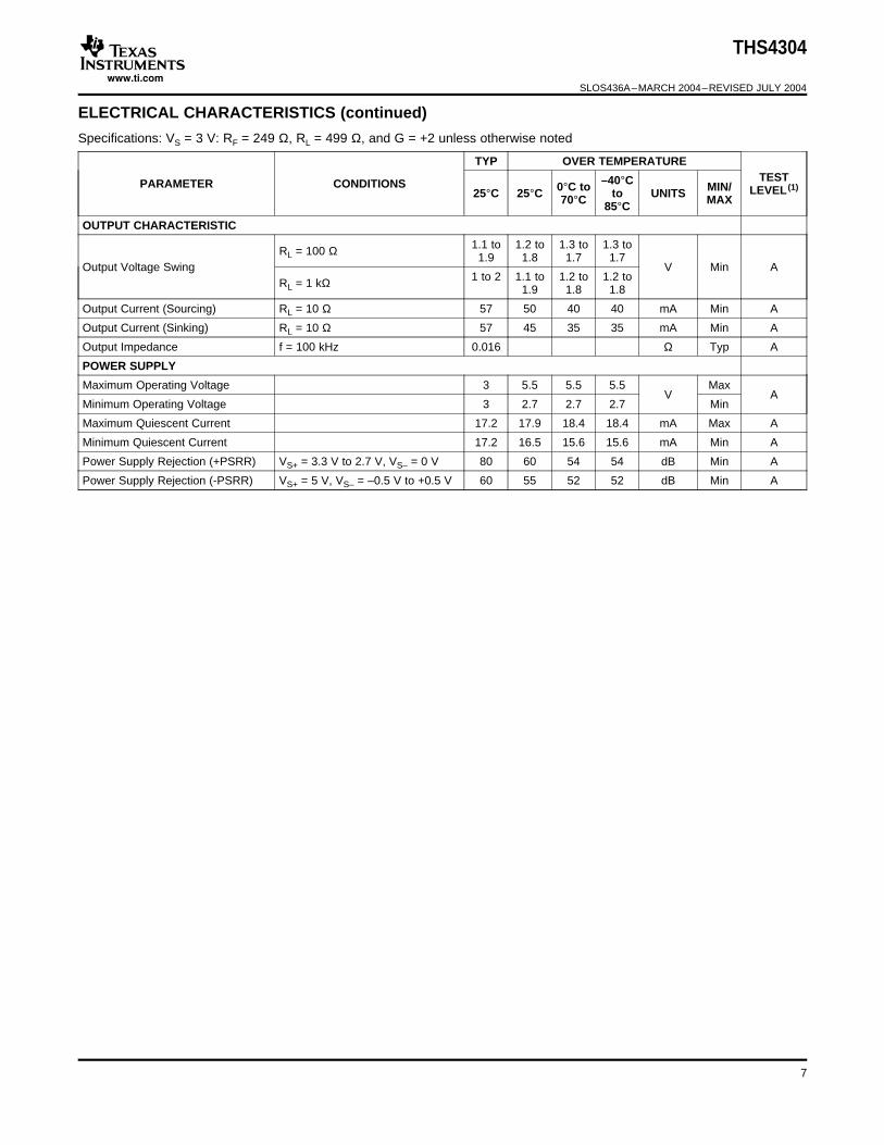
ELECTRICAL CHARACTERISTICS (continued)
Specifications: VS = 3 V: RF = 249 Ω, RL = 499 Ω, and G = +2 unless otherwise noted
TYP OVER TEMPERATURETEST–40°CPARAMETER CONDITIONS 0°C to MIN/ LEVEL (1)
25°C 25°C to UNITS70°C MAX85°C
OUTPUT CHARACTERISTIC
1.1 to 1.2 to 1.3 to 1.3 toRL = 100 Ω 1.9 1.8 1.7 1.7Output Voltage Swing V Min A
1 to 2 1.1 to 1.2 to 1.2 toRL = 1 kΩ 1.9 1.8 1.8
Output Current (Sourcing) RL = 10 Ω 57 50 40 40 mA Min A
Output Current (Sinking) RL = 10 Ω 57 45 35 35 mA Min A
Output Impedance f = 100 kHz 0.016 Ω Typ A
POWER SUPPLY
Maximum Operating Voltage 3 5.5 5.5 5.5 MaxV A
Minimum Operating Voltage 3 2.7 2.7 2.7 Min
Maximum Quiescent Current 17.2 17.9 18.4 18.4 mA Max A
Minimum Quiescent Current 17.2 16.5 15.6 15.6 mA Min A
Power Supply Rejection (+PSRR) VS+ = 3.3 V to 2.7 V, VS– = 0 V 80 60 54 54 dB Min A
Power Supply Rejection (-PSRR) VS+ = 5 V, VS– = –0.5 V to +0.5 V 60 55 52 52 dB Min A
7

www.ti.com
TYPICAL CHARACTERISTICS
THS4304
SLOS436A–MARCH 2004–REVISED JULY 2004
Table of Graphs
FIGURE
5 V
Frequency response 1–3, 5, 6
0.1-dB Flatness 4
Frequency response by package 7
S-Parameters vs Frequency 8
2nd Harmonic distortion vs Frequency 9, 11
3rd Harmonic distortion vs Frequency 10, 12
2nd Harmonic distortion vs Output voltage 13
3rd Harmonic distortion vs Output voltage 14
IMD3 3rd Order intermodulation distortion vs Frequency 15
OIP3 3rd Order output intercept point vs Frequency 16
SR Slew rate vs Output voltage 17
Vn/In Noise vs Frequency 18
Noise figure vs Frequency 19
Iq Quiescent current vs Supply voltage 20
Rejection ratio vs Frequency 21
VO Output voltage vs Load resistance 22
VOS Input offset voltage vs Input common-mode voltage 23
IIB Input bias and offset current vs Case temperature 24
VOS Input offset voltage vs Case temperature 25
Open-loop gain vs Frequency 26
VO Small-signal transient response 27
VO Large-signal transient response 28
VO Settling time 29
VO Overdrive recovery time 30
ZO Output impedance vs Frequency 31
3 V
Frequency response 32–35
2nd Harmonic distortion vs Frequency 36
3rd Harmonic distortion vs Frequency 37
Harmonic Distortion vs Output voltage 38
SR Slew rate vs Output voltage 39
VO Settling time 40
VO Output voltage vs Load resistance 41
IIB Input bias and offset current vs Case temperature 42
VOS Input offset voltage vs Case temperature 43
VO Large-signal transient response 44
VO Overdrive recovery time 45
ZO Output impedance vs Frequency 46
8

www.ti.com
TYPICAL CHARACTERISTICS (5 V)
−4
−3
−2
−1
0
1
2
3
4
5
6
1 M 10 M 100 M 1 G 10 G
Sig
nal
Gai
n −
dB
f − Frequency − Hz
VO = 100 mVPP
VO = 200 mVPP
VO = 400 mVPP
VO = 800 mVPP
3 GHz
Gain = 1,RL = 100 Ω,VS = 5 V
−4
−20
2
4
6
8
1012
14
16
182022
24
100 k 1 M 10 M 100 M 1 G 10 G
Sig
nal
Gai
n −
dB
f − Frequency − Hz
G = 10
G = 5
G = 2
G = 1, RF = 0 Ω
RF = 249 Ω,RL = 100 Ω,VO = 100 mVPPVS = 5 V
0
1
2
3
4
5
6
7
8
9
10
1 M 10 M 100 M 1 G 10 G
CF = 0 pF
CF = 0.5 pF
CF = 1 pF
1 GHz
Gain = 2,RF = 249 Ω,RL = 100 Ω,VO = 100 mVPP,VS = 5 V
f − Frequency − Hz
Sig
nal
Gai
n −
dB
−4−2
0
2
4
6
8
10
12
14
16
18
20
22
1 M 10 M 100 M 1 G 10 G
Sig
nal
Gai
n −
dB
f − Frequency − Hz
RF = 249 Ω,RL = 100 Ω,VO = 1 VPP,
VS = 5 V
90 MHz
200 MHz
480 MHz
560 MHz
RF = 0 Ω
−4
−20
2
4
6
8
10
12
14
16
18
20
22
1 M 10 M 100 M 1 G 10 G
87 MHzRF = 249 Ω,RL = 100 Ω,VO = 2 VPP,
VS = 5 V
175 MHz
240 MHz
290 MHz
Sig
nal
Gai
n −
dB
f − Frequency − Hz
RF = 0 Ω
5.6
5.7
5.8
5.9
6
6.1
6.2
6.3
6.4
1 M 10 M 100 M 1 G
Sig
nal
Gai
n −
dB
f − Frequency − Hz
Gain = 2,RF = 249 Ω,CF = 0.5 pF,RL = 100 Ω,VO = 100 mVPP,
VS = 5 V 300 MHz
−100
−80
−60
−40
−20
0
1 M 10 M 100 M 1 G 10 G
Sig
nal
Gai
n −
dB
f − Frequency − Hz
Gain = 2,RF = 249 Ω,RL = 100 Ω,VO = 100 mVPP,
VS = 5 V
S21
S22
S11 S12
0
1
2
3
4
5
6
7
8
9
10
1 M 10 M 100 M 1 G 10 G
SOIC
SOT-23
MSOP
Sig
nal
Gai
n −
dB
f − Frequency − Hz
Gain = 2,RF = 249 Ω,RL = 100 Ω,VO = 100 mVPP,
VS = 5 V
−110
−100
−90
−80
−70
−60
−50
−40
1 M 10 M 100 M
2nd
Har
mo
nic
Dis
tort
ion
− d
Bc
f − Frequency − Hz
Gain = 2RF = 249 ΩVO = 2 VPPVS = 5 V
MSOP RL = 100 Ω
SOT-23 RL = 100 Ω
MSOP and SOT-23 RL = 499 to 1 k Ω
THS4304
SLOS436A–MARCH 2004–REVISED JULY 2004
FREQUENCY RESPONSE FREQUENCY RESPONSE FREQUENCY RESPONSE
Figure 1. Figure 2. Figure 3.
0.1-dB FLATNESS FREQUENCY RESPONSE FREQUENCY RESPONSE
Figure 4. Figure 5. Figure 6.
S-PARAMETERS 2ND HARMONIC DISTORTIONFREQUENCY RESPONSE vs vs
BY PACKAGE FREQUENCY FREQUENCY
Figure 7. Figure 8. Figure 9.
9
www.ti.com
−110
−100
−90
−80
−70
−60
−50
−40
−30
1 M 10 M 100 M
MSOP and SOT-23RL = 100 Ω to 1 kΩ
Gain = 2,RF = 249 Ω,VO = 2 VPP,VS = 5 V
3rd
Har
mo
nic
Dis
tort
ion
− d
Bc
f − Frequency − Hz
−110
−100
−90
−80
−70
−60
−50
−40
1 M 10 M 100 M
MSOP and SOT-23RL = 100 Ω to 1 kΩ
Gain = 2,RF = 249 Ω,VO = 1 VPP,VS = 5 V
3rd
Har
mo
nic
Dis
tort
ion
− d
Bc
f − Frequency − Hz
−110
−100
−90
−80
−70
−60
−50
−40
1 M 10 M 100 M
2nd
Har
mo
nic
Dis
tort
ion
− d
Bc
f − Frequency − Hz
Gain = 2RF = 249 ΩVO = 1 VPPVS = 5 V
MSOP RL = 100 Ω
SOT-23 RL = 100 Ω
MSOP and SOT-23 RL = 499 Ω to 1 kΩ
−110
−100
−90
−80
−70
−60
−50
−40
−30
0 0.5 1 1.5 2 2.5 3
Gain = 2,RF = 249 Ω,RL = 100 Ω,f = 10 MHz,VS = 5 V
3rd
Har
mo
nic
Dis
tort
ion
− d
Bc
VO − Output Voltage − VPP
SOT-23 RL = 100 Ω to 1 kΩ
−110
−100
−90
−80
−70
−60
−50
−40
0 0.5 1 1.5 2 2.5 3
Gain = 2,RF = 249 Ω,RL = 100 Ω,f = 10 MHz,VS = 5 V
3rd
Har
mo
nic
Dis
tort
ion
− d
Bc
VO − Output Voltage − VPP
SOT-23 RL = 100 Ω
SOT-23 RL = 499 Ω to 1 kΩ−110
−100
−90
−80
−70
−60
−50
−40
−30
10 M 100 M
VO = 2 VPPenvelope
VO = 1 VPPenvelope
− d
Bc
IMD
3
f − Frequency − Hz
Gain = 2,RF = 249 Ω,RL = 100 Ω,200 kHz Spacing,VS = 5 V
1
10
100
1000
10 100 1 k 10 k 100 k 1 M 10 M
f − Frequency − Hz
nV
/H
z−
Volt
age
No
ise
−V
n
I n−
Cu
rren
t N
ois
e −
pA
/H
z
Vn
In
10
20
30
40
50
60
10 M 100 M
− d
Bm
OIP
3
f − Frequency − Hz
Gain = 2,RF = 249 Ω,RL = 100 Ω,VO = 2−VPP envelope,200−kHz Spacing,VS = 5 V
400
450
500
550
600
650
700
750
800
850
900
0 0.5 1 1.5 2 2.5 3
Gain = 2,RF = 249 Ω,RL = 100 Ω,VS = 5 V
SR
− S
lew
Rat
e −
V/
VO − Output Voltage −VPP
sµ
Rise
Fall
THS4304
SLOS436A–MARCH 2004–REVISED JULY 2004
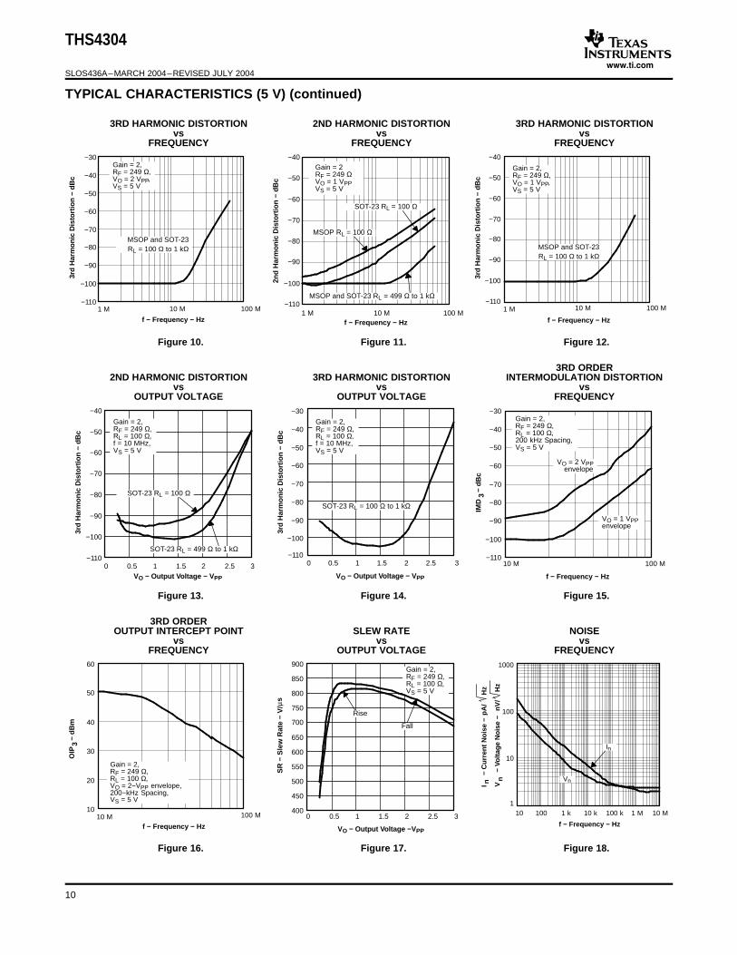
TYPICAL CHARACTERISTICS (5 V) (continued)
3RD HARMONIC DISTORTION 2ND HARMONIC DISTORTION 3RD HARMONIC DISTORTIONvs vs vs
FREQUENCY FREQUENCY FREQUENCY
Figure 10. Figure 11. Figure 12.
3RD ORDER2ND HARMONIC DISTORTION 3RD HARMONIC DISTORTION INTERMODULATION DISTORTION
vs vs vsOUTPUT VOLTAGE OUTPUT VOLTAGE FREQUENCY
Figure 13. Figure 14. Figure 15.
3RD ORDEROUTPUT INTERCEPT POINT SLEW RATE NOISE
vs vs vsFREQUENCY OUTPUT VOLTAGE FREQUENCY
Figure 16. Figure 17. Figure 18.
10
www.ti.com
0
2
4
6
8
10
12
14
16
18
20
10 M 500 M 1 G
No
ise
Fig
ure
− d
B
f − Frequency − Hz
Gain = 2,RF = 249 Ω,RG = 249 Ω,RL = 100 Ω,VS = 5 V
0
2
4
6
8
10
12
14
16
18
20
22
2 2.5 3 3.5 4 4.5 5
I−
Qu
iesc
ent
Cu
rren
t −
mA
VS − Supply Voltage − V
TA = 85°C
TA = −40°C
TA = 25°C
q
0
10
20
30
40
50
60
70
80
90
100
110
10 k 100 k 1 M 10 M 100 M 1 G
f − Frequency − Hz
Rej
ecti
on
Rat
io −
dB
CMRR
PSRR+
PSRR−
VS = 5 V
0
1
2
3
4
5
6
7
8
9
−40−30−20−10 0 10 20 30 40 50 60 70 80 90100
120
140
160
180
200
220
240
260
280
IIB−
IIB+
IOS
VS = 5 V
I IB
− In
pu
t B
ias
Cu
rren
t −
Aµ
− In
pu
t O
ffse
t C
urr
ent
− n
A
I OS
Case Temperature − °C
1
1.5
2
2.5
3
3.5
4
10 100 1000
VS = 5 V
RL − Load Resistance − Ω
− O
utp
ut V
olt
age
− V
V O
0
0.5
1
1.5
2
2.5
3
3.5
4
4.5
5
−1 0 1 2 3 4 5 6
− In
pu
t O
ffse
t Vo
ltag
e −
mV
VO
S
VICR − Input Common-Mode Range − V
VS = 5 V
2.2
2.3
2.4
2.5
2.6
2.7
2.8
2.9
0 10 20 30 40 50 60
2.3
2.4
2.5
2.6
2.7
2.8
t − Time − ns
− O
utp
ut V
olt
age
− V
V O
Gain = 2RL = 100 ΩRF = 249 Ωtr/tf = 300 psVS = 5 V
− In
pu
t Vo
ltag
e −
VV
IInput
Output
−20
−10
0
10
20
30
40
50
60
70
80
10 k 100 k 1 M 10 M 100 M 1 G 10 G−180
−160
−140
−120
−100
−80
−60
−40
−20
0
20
Op
en-L
oo
p G
ain
− d
B
f − Frequency − Hz
Ph
ase
−°
Gain
Phase
VS = 5 V
0
100
200
300
400
500
600
−40−30−20−10 0 10 20 30 40 50 60 70 80 90
− In
pu
t O
ffse
t Vo
ltag
e −
VO
SV
µ
VS = 5 V
Case Temperature − °C
THS4304
SLOS436A–MARCH 2004–REVISED JULY 2004
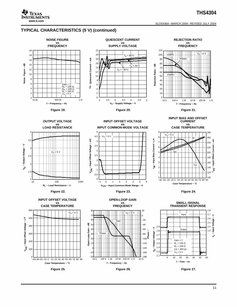
TYPICAL CHARACTERISTICS (5 V) (continued)
NOISE FIGURE QUIESCENT CURRENT REJECTION RATIOvs vs vs
FREQUENCY SUPPLY VOLTAGE FREQUENCY
Figure 19. Figure 20. Figure 21.
INPUT BIAS AND OFFSETOUTPUT VOLTAGE INPUT OFFSET VOLTAGE CURRENT
vs vs vsLOAD RESISTANCE INPUT COMMON-MODE VOLTAGE CASE TEMPERATURE
Figure 22. Figure 23. Figure 24.
INPUT OFFSET VOLTAGE OPEN-LOOP GAINvs vs SMALL-SIGNAL
CASE TEMPERATURE FREQUENCY TRANSIENT RESPONSE
Figure 25. Figure 26. Figure 27.
11
www.ti.com
1
1.5
2
2.5
3
3.5
4
0 10 20 30 40 50 60
1.5
2
2.5
3
3.5
t − Time − ns
− O
utp
ut V
olt
age
− V
V O
Gain = 2RL = 100 ΩRF = 249 ΩVS = 5 V
− In
pu
t Vo
ltag
e −
VV
I
Input
Output
0.5
1
1.5
2
2.5
3
3.5
4
4.5
0 0.1 0.2 0.3 0.4 0.5 0.6 0.71.5
1.75
2
2.25
2.5
2.75
3
3.25
3.5
t − Time − µs
− In
pu
t Vo
ltag
e −
VV
I− O
utp
ut V
olt
age
− V
V O
Gain = 2RL = 100 ΩRF = 249 ΩVS = 5 V
Input
Output
1
1.5
2
2.5
3
3.5
4
0 1 2 3 4 5 6 7
− O
utp
ut V
olt
age
− V
VO
t − Time − ns
Gain = 2RL = 100 ΩRF = 249 ΩVS = 5 V
0.01
0.1
1
10
100
1 k
10 k
100 k 1 M 10 M 100 M 1 G
f − Frequency − Hz
Gain = 2,RF = 249 Ω,VS = 5 V
− O
utp
ut
Imp
edan
ce −
Zo
Ω
THS4304
SLOS436A–MARCH 2004–REVISED JULY 2004
TYPICAL CHARACTERISTICS (5 V) (continued)
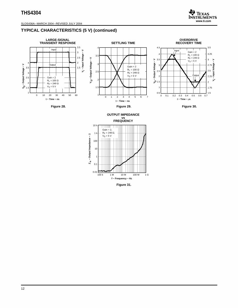
LARGE-SIGNAL OVERDRIVETRANSIENT RESPONSE SETTLING TIME RECOVERY TIME
Figure 28. Figure 29. Figure 30.
OUTPUT IMPEDANCEvs
FREQUENCY
Figure 31.
12
www.ti.com
TYPICAL CHARACTERISTICS (3 V)
0
1
2
3
4
5
6
7
8
9
10
10 M 100 M 1 G 10 G
CF = 0 pF
CF = 0.5 pF
CF = 1 pF
Gain = 2RL = 499 ΩRF = 249 Ω,VO = 100 mVPP,VS = 3 V
Sig
nal
Gai
n −
dB
f − Frequency − Hz
0
1
2
3
4
5
6
7
8
9
10
10 M 100 M 1 G 10 G
Sig
nal
Gai
n −
dB
f − Frequency − Hz
Gain = 2RL = 499 ΩRF = 249 Ω,VS = 3 V
VO = 100 mVPP
VO = 200 mVPP
−3dB 900 MHz
VO = 400 mVPP
VO = 800 mVPP
−4
−20
2
4
68
10
1214
16
18
2022
24
1 M 10 M 100 M 1 G 10 G
G 10
G 5
G 2
G 1, RF 0Ω
RF = 249 Ω,RL = 499 Ω,VO = 100 mVPP,VS = 3 V
Sig
nal
Gai
n −
dB
f − Frequency − Hz
−4
−20
2
4
6
8
10
12
14
16
18
20
22
1 M 10 M 100 M 1 G
RF = 249 Ω,RL = 499 Ω,VO = 1 VPP,VS = 3 V
Sig
nal
Gai
n −
dB
f − Frequency − Hz
−3 dB 85 MHz
−3 dB 90 MHz
−3 dB 450 MHz
−100
−90
−80
−70
−60
−50
1 M 10 M 100 M
2nd
Har
mo
nic
Dis
tort
ion
− d
Bc
f − Frequency − Hz
Gain = 2RL = 499 ΩRF = 249 Ω,VO = 500 mVPP,VS = 3 V
−100
−90
−80
−70
−60
−50
1 M 10 M 100 M
f − Frequency − Hz
3rd
Har
mo
nic
Dis
tort
ion
− d
Bc
Gain = 2RL = 499 ΩRF = 249 Ω,VO = 500 mVPP,VS = 3 V
1.25
1.35
1.45
1.55
1.65
1.75
0 1 2 3 4 5 6 7 8 9 10
− O
utp
ut V
olt
age
− V
VO
t − Time − ns
Gain = 2RL = 499 ΩRF = 249 ΩVS = 3 V
−100
−90
−80
−70
−60
−50
−40
0 0.1 0.2 0.3 0.4 0.5 0.6 0.7 0.8 0.9 1
Har
mo
nic
Dis
tort
ion
− d
Bc
HD 2
HD 3
Gain = 2RL = 499 ΩRF = 249 Ω,f = 10 MHz,VS = 3 V
VO − Output Voltage − VPP
400
450
500
550
600
650
700
750
800
850
900
0 0.1 0.2 0.3 0.4 0.5 0.6
Rise
Fall
Gain = 2,RF = 249 Ω,RL = 499 Ω,VS = 3 V
SR
− S
lew
Rat
e −
V/µ
s
VO − Output Voltage − VPP
THS4304
SLOS436A–MARCH 2004–REVISED JULY 2004
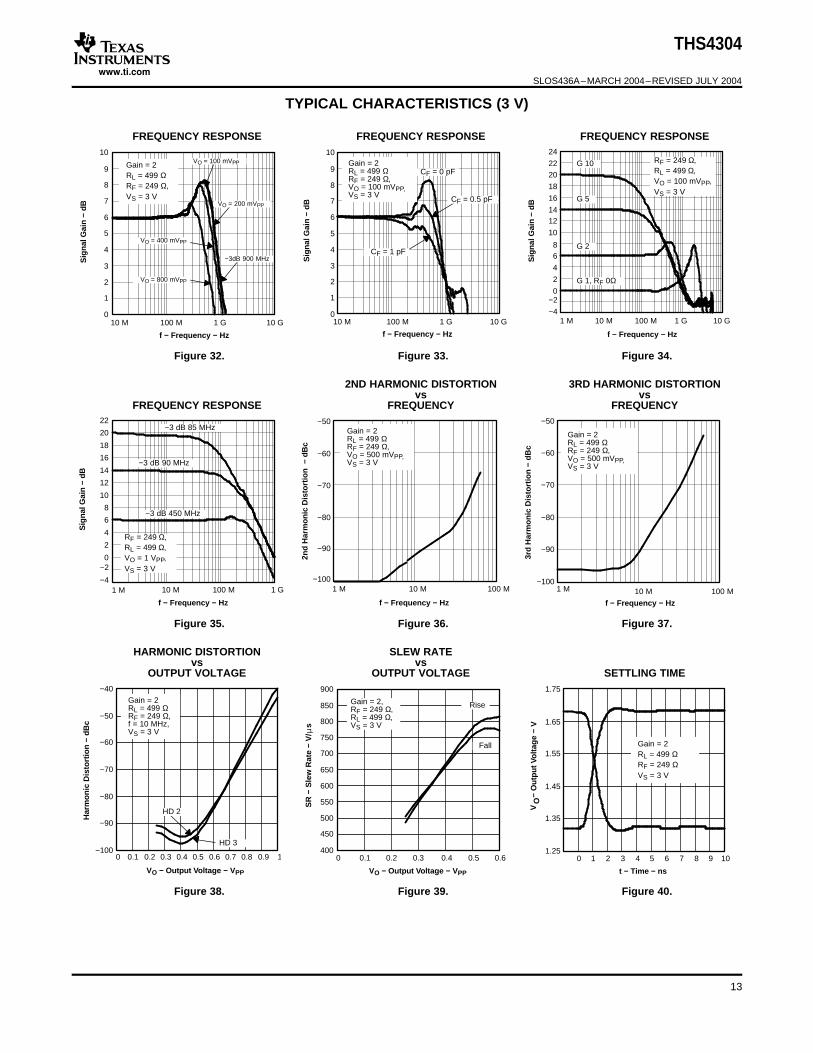
FREQUENCY RESPONSE FREQUENCY RESPONSE FREQUENCY RESPONSE
Figure 32. Figure 33. Figure 34.
2ND HARMONIC DISTORTION 3RD HARMONIC DISTORTIONvs vs
FREQUENCY RESPONSE FREQUENCY FREQUENCY
Figure 35. Figure 36. Figure 37.
HARMONIC DISTORTION SLEW RATEvs vs
OUTPUT VOLTAGE OUTPUT VOLTAGE SETTLING TIME
Figure 38. Figure 39. Figure 40.
13

www.ti.com
0
1
2
3
4
5
6
7
8
9
−40 −20 0 20 40 60 80460
480
500
520
540
560
580
600
620
640
IIB−
IIB+
VS = 3 V
IOS
I IB
− In
pu
t B
ias
Cu
rren
t −
Aµ
− In
pu
t O
ffse
t C
urr
ent
− n
A
I OS
TC − Case Temperature − °C
0.5
0.75
1
1.25
1.5
1.75
2
2.25
10 100 1000
− O
utp
ut V
olt
age
− V
VO
RL − Load Resistance −
VS = 3 V
1
1.25
1.5
1.75
2
2.25
2.5
−40 −20 0 20 40 60 80
TC − Case Temperature − °C
− In
pu
t O
ffse
t Vo
ltag
e −
mV
VO
S
VS = 3 V
0.5
0.75
1
1.25
1.5
1.75
2
2.25
0 0.1 0.2 0.3 0.4 0.5 0.6 0.7 0.8 0.9 10.5
0.75
1
1.25
1.5
1.75
2
2.25
Input
Output
t − Time − µs
− In
pu
t Vo
ltag
e −
VI
G = 2,RL = 499 Ω,RF = 249 Ω,VS = 3 V
− O
utp
ut V
olt
age
− V
OV
PP
VP
P
0
0.5
1
1.5
2
2.5
3
−10 0 10 20 30 40 50 60
0.5
1
1.5
2
2.5
t − Time − ns
− O
utp
ut V
olt
age
− V
V O
Gain = 2,RF = 249 Ω,RL = 499 Ω,VS = 3 V
− In
pu
t Vo
ltag
e −
VV
I
Input
Output
0.01
0.1
1
10
100
1 k
10 k
100 k 1 M 10 M 100 M 1 G
f − Frequency − Hz
Gain = 2,RF = 249 Ω,VS = 3 V
− O
utp
ut
Imp
edan
ce −
Zo
Ω
THS4304
SLOS436A–MARCH 2004–REVISED JULY 2004
TYPICAL CHARACTERISTICS (3 V) (continued)
INPUT BIAS ANDOUTPUT VOLTAGE OFFSET CURRENT INPUT OFFSET VOLTAGE
vs vs vsLOAD RESISTANCE CASE TEMPERATURE CASE TEMPERATURE
Figure 41. Figure 42. Figure 43.
OUTPUT IMPEDANCELARGE-SIGNAL vs
TRANSIENT RESPONSE OVERDRIVE RECOVERY TIME FREQUENCY
Figure 44. Figure 45. Figure 46.
14
www.ti.com
APPLICATION INFORMATION
For many years, high-performance analog design has required the generation of split power supply voltages, like
SNR
SignalNoise
SFDR
SignalSpur
GENERAL APPLICATION
HARMONIC DISTORTION
THS4304
SLOS436A–MARCH 2004–REVISED JULY 2004
±15 V, ±8 V, and more recently ±5 V, in order to realize the full performance of the amplifiers available. Moderntrends in high-performance analog are moving towards single-supply operation at 5 V, 3 V, and lower. Thisreduces power supply cost due to less voltages being generated and conserves energy in low powerapplications. It can also take a toll on available dynamic range, a valuable commodity in analog design, if theavailable voltage swing of the signal must also be reduced.
Two key figures of merit for dynamic range are signal-to-noise ratio (SNR) and spurious free dynamic range(SFDR).
SNR is simply the signal level divided by the noise:
and SFDR is the signal level divided by the highest spur:
In an operational amplifier, reduced supply voltage typically results in reduced signal levels due to lower voltageavailable to operate the transistors within the amplifier. When noise and distortion remain constant, the result is acommensurate reduction in SNR and SFDR. To regain dynamic range, the process and the architecture used tomake the operational amplifier must have superior noise and distortion performance with lower power supplyoverhead required for proper transistor operation.
The THS4304 BiCom3 operational amplifier is just such a device. It is able to provide 2-Vpp signal swing at itsoutput on a single 5-V supply with noise and distortion performance similar to the best 10-V operationalamplifiers on the market today
The THS4304 is a traditional voltage-feedback topology with wideband performance up to 3 GHz at unity gain.Care must be taken to ensure that parasitic elements do not erode the phase margin.
Capacitance at the output and inverting input, and resistance and inductance in the feedback path, can causeproblems.
To reduce parasitic capacitance, the ground plane should be removed from under the part.
To reduce inductance in the feedback, the circuit traces should be kept as short and direct as possible. For bestperformance in non-inverting unity gain (G=+1V/V), it is recommended to use a wide trace directly between theoutput and inverting input.
For a gain of +2V/V, it is recommended to use a 249-Ω feedback resistor. With good layout, this should keep thefrequency response peaking to around 2 dB. This resistance is high enough to not load the output excessively,and the part is capable of driving 100-Ω load with good performance. Higher-value resistors can be used, withmore peaking. For example, 499 Ω gives about 5 dB of peaking, and gives slightly better distortion performancewith 100-Ω load. Lower value feedback resistors can also be used to reduce peaking, but degrades the distortionperformance with heavy loads.
Power supply bypass capacitors are required for proper operation. The most critical are 0.1-µF ceramiccapacitors; these should be placed as close to the part as possible. Larger bulk capacitors can be shared withother components in the same area as the operational amplifier.
For best second harmonic (HD2), it is important to use a single-point ground between the power supply bypasscapacitors when using a split supply. It is also recommended to use a single ground or reference point for inputtermination and gain-setting resistors (R8 and R11 in the non-inverting circuit). It is recommended to follow theEVM layout closely in your application.
15

www.ti.com
SOT-23 versus MSOP
EVALUATION MODULES
1
2
43
5
VREF
R3 R6+VS
C8 R8 C3
R7
+VS
U1
R9
C7J1 R10
R11 R1
VREF
−VS
THS4304 R2 C9 J2
C5 C1
−VSFB1 FB2
J3 J4 J6 J5
−VS +VSGND GND
+VS
TP1GND
C2 C4
R12*
C6*−VS +VS
*C6 − DGK EVM Only
*R12 − DBV EVM Only
THS4304
SLOS436A–MARCH 2004–REVISED JULY 2004
APPLICATION INFORMATION (continued)
With light loading of 500-Ω and higher resistance, the THS4304 shows HD2 that is not dependant of package.With heavy output loading of 100 Ω, the THS4304 in SOT-23 package shows about 6 dB better HD2performance versus the MSOP package.
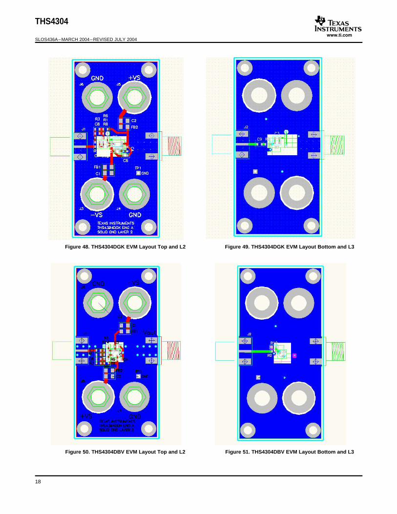
The THS4304 has two evaluation modules (EVMs) available. One is for the MSOP (DGK) package and the otherfor the SOT-23 (DBV) package. These provide a convenient platform for evaluating the performance of the partand building various different circuits. The full schematics, board layout, and bill of materials (as supplied) for theboards are shown in the following illustrations.
Figure 47. EVM Full Schematic
16

www.ti.com
THS4304
SLOS436A–MARCH 2004–REVISED JULY 2004
APPLICATION INFORMATION (continued)
EVM BILL OF MATERIALS
THS4304 EVM (1)
SMD Reference PCB Manufacturer's Distributor'sItem Description Size Designator Quantity Part Number Part Number
1 FB1, FB2 2 (STEWARD) (DIGI-KEY)Bead, ferrite, 3-A, 80-Ω 1206 HI1206N800R-00 240-1010-1-ND
2 Capacitor, 3.3-µF, Ceramic 1206 C1, C2 2 (AVX) 1206YG335ZAT2A (GARRETT)1206YG335ZAT2A
3 Capacitor, 0.1-µF, Ceramic 0603 C4, C5 2 (AVX) 0603YC104KAT2A (GARRETT)0603YC104KAT2A
4 Open 0603 C3, C6 (2) 2
5 Open 0603 R1, R3, R6, 5R9, R12 (3)
6 Resistor, 0-Ω, 1/10-W, 1% 0603 C7. C8, C9, 4 (KOA) RK73Z1JTTD (GARRETT)C10 RK73Z1JTTD
7 Resistor, 49.9-Ω, 1/10-W, 1% 0603 R2, R11 2 (KOA) RK73H1JLTD49R9F (GARRETT)RK73H1JLTD49R9F
8 Resistor, 249-Ω, 1/10-W, 1% 0603 R7, R8 2 (KOA) RK73H1JLTD2490F (GARRETT)RK73H1JLTD2490F
9 Jack, banana recepticle, 0.25-in. di- J3, J4, J5, J6 4 (HH SMITH) 101 (NEWARK) 35F865ameter hole
10 Test point, black TP1 1 (KEYSTONE) 5001 (DIGI-KEY) 5001K-ND
11 Connector, edge, SMA PCB jack J1, J2 2 (JOHNSON) 142-0701-801 (NEWARK) 90F2624
12 Integrated Circuit, THS4304 U1 1 (TI) THS4304DGK, or(TI) THS4304DBV
13 Standoff, 4-40 HEX, 0.625-in. 4 (KEYSTONE) 1808 NEWARK) 89F1934Length
14 Screw, Phillips, 4-40, 0.250-in. 4 SHR-0440-016-SN
15 Board, printed-circuit 1 (TI) THS4304DGK ENG A, or(TI) THS4304DBV ENG A
(1) NOTE: All items are designated for both the DBV and DGK EVMs unless otherwise noted.(2) C6 used on DGK EVM only.(3) R12 used on DBV EVM only.
17
www.ti.com
THS4304
SLOS436A–MARCH 2004–REVISED JULY 2004
Figure 48. THS4304DGK EVM Layout Top and L2 Figure 49. THS4304DGK EVM Layout Bottom and L3
Figure 50. THS4304DBV EVM Layout Top and L2 Figure 51. THS4304DBV EVM Layout Bottom and L3
18

www.ti.com
NON-INVERTING GAIN WITH SPLIT SUPPLY
1
2
4
3
5
C8
0
R8
249 249
R7
+VS
U1
−VS +VSFB1 FB2
−VS +VSGND GND
J3 J4 J6 J5
C50.1 F
C13.3 F
GND
TP1
C23.3 F
C40.1 F
J1 C7 R10
0 0R1149.9 −VS
THS4304DBV
R2
49.9
C9
0
J2
THS4304
SLOS436A–MARCH 2004–REVISED JULY 2004
The following schematic shows how to configure the operational amplifier for non-inverting gain with split powersupply (± 2.5V). This is how the EVM is supplied from TI. This configuration is convenient for test purposesbecause most signal generators and analyzer are designed to use ground-referenced signals by default. Notethe input and output provides 50-Ω termination.
Figure 52. Non-Inverting Gain with Split Power Supply
19
www.ti.com
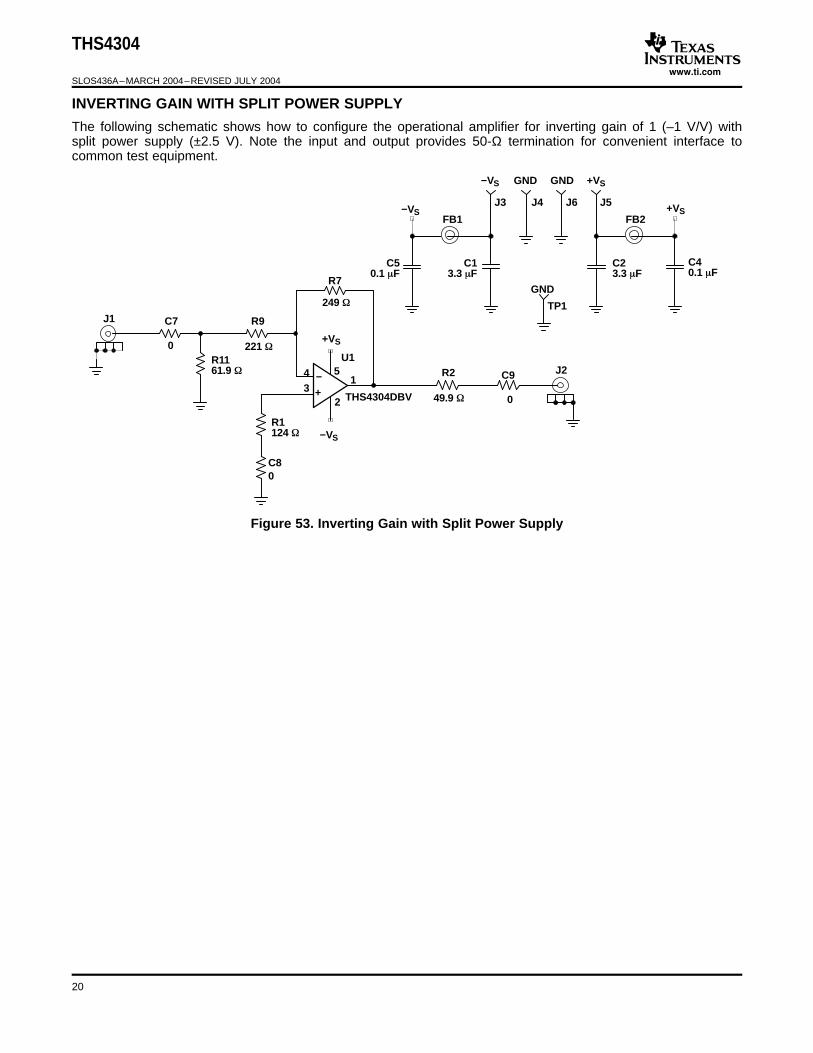
INVERTING GAIN WITH SPLIT POWER SUPPLY
1
2
43
5
−VS +VSFB1 FB2
−VS +VSGND GND
J3 J4 J6 J5
C50.1 F
C13.3 F
GND
TP1
C23.3 F
C40.1 F
+VS
J1 C7 R9
0R1161.9
−VS
THS4304DBV
C9
0
J2
221
R1124
C80
U1R2
49.9
R7
249
51
2
43 +
−
THS4304
SLOS436A–MARCH 2004–REVISED JULY 2004
The following schematic shows how to configure the operational amplifier for inverting gain of 1 (–1 V/V) withsplit power supply (±2.5 V). Note the input and output provides 50-Ω termination for convenient interface tocommon test equipment.
Figure 53. Inverting Gain with Split Power Supply
20

www.ti.com
NON-INVERTING SINGLE-SUPPLY OPERATION
1
2
43
5
+VSFB2
−VS +VSGND GND
J3 J4 J6 J5
GND
TP1
C23.3 F
C40.1 F
NC
C8 R8
249 249
R7
+VS
U1
J1 C7 R10
0 0R149.9
THS4304DBV
R2
49.9
C9
0
J2
VREF
R3
10 k 10 k
R6+VS
0.1 F
C5
VREF
3
41
5
2+
−
DIFFERENTIAL ADC DRIVE AMPLIFIER
THS4304
SLOS436A–MARCH 2004–REVISED JULY 2004
The THS4304 EVM can easily be configured for single 5-V supply operation, as shown in the followingschematic, with no change in performance. This circuit passes dc signals at the input, so care must be taken toreference (or bias) the input signal to mid-supply.
If dc operation is not required, the amplifier can be ac coupled by inserting a capacitor in series with the input(C7) and output (C9).
Figure 54. Non-Inverting 5-V Single-Supply Amplifier
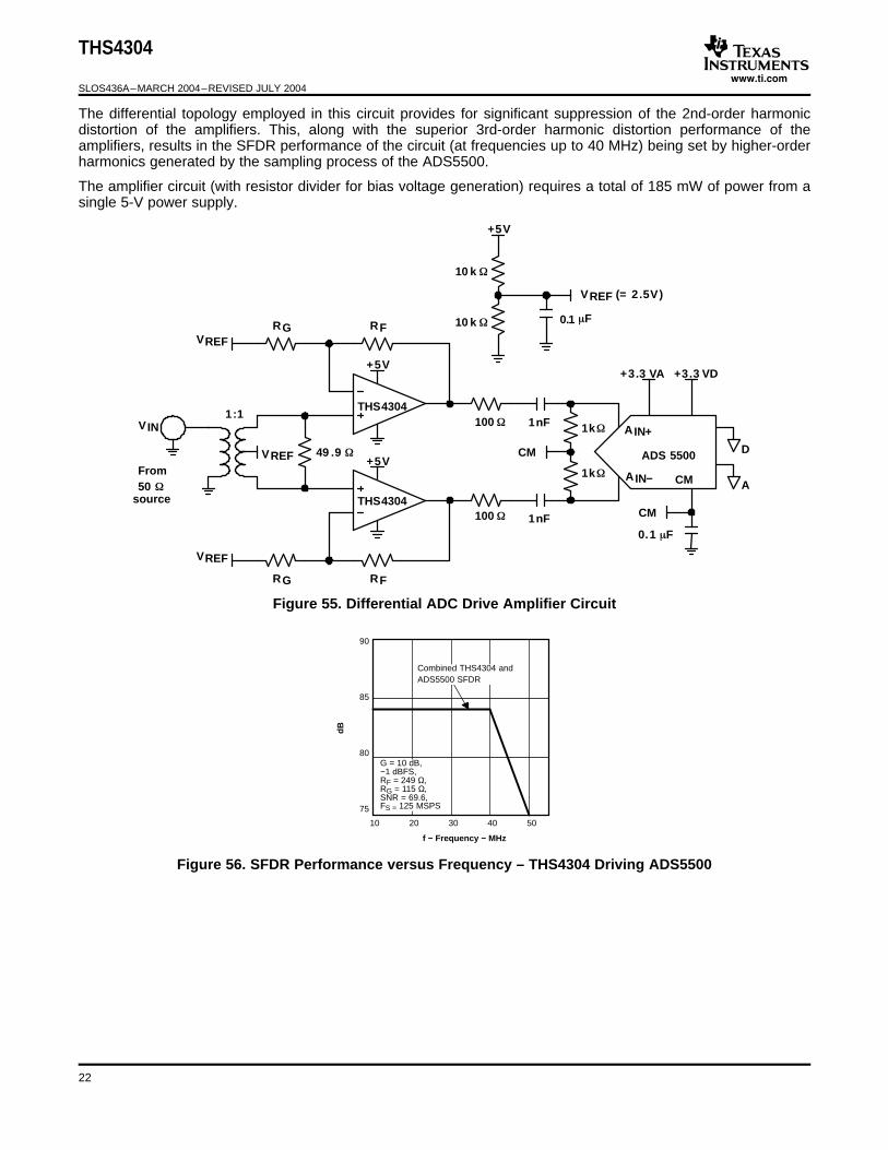
The circuit shown in Figure 54 is adapted as shown in Figure 55 to provide a high-performance differentialamplifier drive circuit for use with high-performance ADCs, like the ADS5500 (14-bit 125-MSP ADC). For testingpurposes, the circuit uses a transformer to convert the signal from a single-ended source to differential. If theinput signal source in your application is differential and biased to mid-rail, no transformer is required.
The circuit employs two amplifiers to provide a differential signal path to the ADS5500. A resistor divider (two10-kΩ resistors) is used to obtain a mid-supply reference voltage of 2.5 V (VREF) (the same as shown in thesingle-supply circuit of Figure 54). Applying this voltage to the one side of RG and to the positive input of theoperational amplifier (via the center-tap of the transformer) sets the input and output common-mode voltage ofthe operational amplifiers to mid-rail to optimize their performance. The ADS5500 requires an inputcommon-mode voltage of 1.5 V. Due to the mismatch in required common-mode voltage, the signal is ac coupledfrom the amplifier output, via the two 1-nF capacitors, to the input of the ADC. The CM voltage of the ADS5500 isused to bias the ADC input to the required voltage, via the 1-kΩ resistors. Note: 100-µA common-mode current isdrawn by the ADS5500 input stage (at 125 MSPS). This causes a 100-mV shift in the input common-modevoltage, which does not impact the performance when driving the input to –1 dB of full scale. To offset this effect,a voltage divider from the power supply can be used to derive the input common-mode voltage reference.
Because the operational amplifiers are configured as non-inverting, the inputs are high impedance. This isparticularly useful when interfacing to a high-impedance source. In this situation, the amplifiers provideimpedance matching and amplification of the signal.
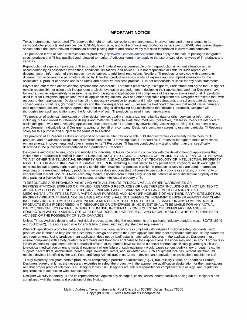
The SFDR performance of the circuit is shown in the following graph (see Figure 56) and provides for fullperformance from the ADS5500 to 40 MHz.
21
www.ti.com
+5V
AIN+
AIN−
ADS 5500
RFRG
49 .9
VIN
From50
source
1001:1
RFRG
CM
CM
0.1
THS4304
THS4304
1k
+3.3 VA +3.3 VD
D
A
0.1
+5V
10 k
VREF (= 2.5V)
VREF
VREF
VREF
1nF
1nF
+5VCM
10 k
100
1k
F
F
75
80
85
90
10 20 30 40 50
dB
f − Frequency − MHz
Combined THS4304 andADS5500 SFDR
G = 10 dB,−1 dBFS,RF = 249 Ω,RG = 115 Ω,SNR = 69.6,FS = 125 MSPS
THS4304
SLOS436A–MARCH 2004–REVISED JULY 2004
The differential topology employed in this circuit provides for significant suppression of the 2nd-order harmonicdistortion of the amplifiers. This, along with the superior 3rd-order harmonic distortion performance of theamplifiers, results in the SFDR performance of the circuit (at frequencies up to 40 MHz) being set by higher-orderharmonics generated by the sampling process of the ADS5500.
The amplifier circuit (with resistor divider for bias voltage generation) requires a total of 185 mW of power from asingle 5-V power supply.
Figure 55. Differential ADC Drive Amplifier Circuit
Figure 56. SFDR Performance versus Frequency – THS4304 Driving ADS5500
22

PACKAGE OPTION ADDENDUM
www.ti.com 24-Aug-2018
Addendum-Page 1
PACKAGING INFORMATION
Orderable Device Status(1)
Package Type PackageDrawing
Pins PackageQty
Eco Plan(2)
Lead/Ball Finish(6)
MSL Peak Temp(3)
Op Temp (°C) Device Marking(4/5)
Samples
THS4304D ACTIVE SOIC D 8 75 Green (RoHS& no Sb/Br)
CU NIPDAU Level-1-260C-UNLIM -40 to 85 4304
THS4304DBVR ACTIVE SOT-23 DBV 5 3000 Green (RoHS& no Sb/Br)
CU NIPDAU Level-1-260C-UNLIM -40 to 85 AKW
THS4304DBVT ACTIVE SOT-23 DBV 5 250 Green (RoHS& no Sb/Br)
CU NIPDAU Level-1-260C-UNLIM -40 to 85 AKW
THS4304DG4 ACTIVE SOIC D 8 75 Green (RoHS& no Sb/Br)
CU NIPDAU Level-1-260C-UNLIM -40 to 85 4304
THS4304DGK ACTIVE VSSOP DGK 8 80 Green (RoHS& no Sb/Br)
CU NIPDAU Level-1-260C-UNLIM -40 to 85 AKU
THS4304DGKR ACTIVE VSSOP DGK 8 2500 Green (RoHS& no Sb/Br)
CU NIPDAU Level-1-260C-UNLIM -40 to 85 AKU
(1) The marketing status values are defined as follows:ACTIVE: Product device recommended for new designs.LIFEBUY: TI has announced that the device will be discontinued, and a lifetime-buy period is in effect.NRND: Not recommended for new designs. Device is in production to support existing customers, but TI does not recommend using this part in a new design.PREVIEW: Device has been announced but is not in production. Samples may or may not be available.OBSOLETE: TI has discontinued the production of the device.
(2) RoHS: TI defines "RoHS" to mean semiconductor products that are compliant with the current EU RoHS requirements for all 10 RoHS substances, including the requirement that RoHS substancedo not exceed 0.1% by weight in homogeneous materials. Where designed to be soldered at high temperatures, "RoHS" products are suitable for use in specified lead-free processes. TI mayreference these types of products as "Pb-Free".RoHS Exempt: TI defines "RoHS Exempt" to mean products that contain lead but are compliant with EU RoHS pursuant to a specific EU RoHS exemption.Green: TI defines "Green" to mean the content of Chlorine (Cl) and Bromine (Br) based flame retardants meet JS709B low halogen requirements of <=1000ppm threshold. Antimony trioxide basedflame retardants must also meet the <=1000ppm threshold requirement.
(3) MSL, Peak Temp. - The Moisture Sensitivity Level rating according to the JEDEC industry standard classifications, and peak solder temperature.
(4) There may be additional marking, which relates to the logo, the lot trace code information, or the environmental category on the device.
(5) Multiple Device Markings will be inside parentheses. Only one Device Marking contained in parentheses and separated by a "~" will appear on a device. If a line is indented then it is a continuationof the previous line and the two combined represent the entire Device Marking for that device.

PACKAGE OPTION ADDENDUM
www.ti.com 24-Aug-2018
Addendum-Page 2
(6) Lead/Ball Finish - Orderable Devices may have multiple material finish options. Finish options are separated by a vertical ruled line. Lead/Ball Finish values may wrap to two lines if the finishvalue exceeds the maximum column width.
Important Information and Disclaimer:The information provided on this page represents TI's knowledge and belief as of the date that it is provided. TI bases its knowledge and belief on informationprovided by third parties, and makes no representation or warranty as to the accuracy of such information. Efforts are underway to better integrate information from third parties. TI has taken andcontinues to take reasonable steps to provide representative and accurate information but may not have conducted destructive testing or chemical analysis on incoming materials and chemicals.TI and TI suppliers consider certain information to be proprietary, and thus CAS numbers and other limited information may not be available for release.
In no event shall TI's liability arising out of such information exceed the total purchase price of the TI part(s) at issue in this document sold by TI to Customer on an annual basis.
OTHER QUALIFIED VERSIONS OF THS4304 :
• Space: THS4304-SP
NOTE: Qualified Version Definitions:
• Space - Radiation tolerant, ceramic packaging and qualified for use in Space-based application
TAPE AND REEL INFORMATION
*All dimensions are nominal
Device PackageType
PackageDrawing
Pins SPQ ReelDiameter
(mm)
ReelWidth
W1 (mm)
A0(mm)
B0(mm)
K0(mm)
P1(mm)
W(mm)
Pin1Quadrant
THS4304DBVR SOT-23 DBV 5 3000 180.0 9.0 3.15 3.2 1.4 4.0 8.0 Q3
THS4304DBVT SOT-23 DBV 5 250 180.0 9.0 3.15 3.2 1.4 4.0 8.0 Q3
THS4304DGKR VSSOP DGK 8 2500 330.0 12.4 5.3 3.4 1.4 8.0 12.0 Q1
PACKAGE MATERIALS INFORMATION
www.ti.com 16-Sep-2017
Pack Materials-Page 1
*All dimensions are nominal
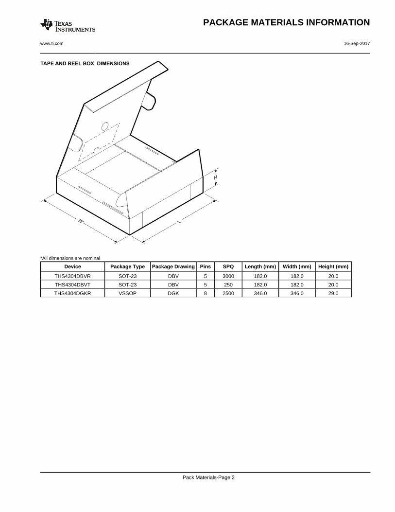
Device Package Type Package Drawing Pins SPQ Length (mm) Width (mm) Height (mm)
THS4304DBVR SOT-23 DBV 5 3000 182.0 182.0 20.0
THS4304DBVT SOT-23 DBV 5 250 182.0 182.0 20.0
THS4304DGKR VSSOP DGK 8 2500 346.0 346.0 29.0
PACKAGE MATERIALS INFORMATION
www.ti.com 16-Sep-2017
Pack Materials-Page 2

www.ti.com
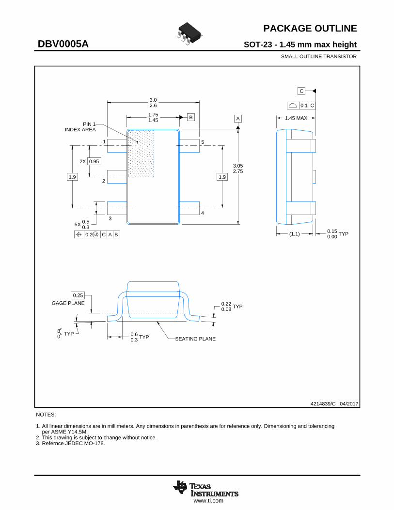
PACKAGE OUTLINE
C
TYP0.220.08
0.25
3.02.6
2X 0.95
1.9
1.45 MAX
TYP0.150.00
5X 0.50.3
TYP0.60.3
TYP80
1.9
A
3.052.75
B1.751.45
(1.1)
SOT-23 - 1.45 mm max heightDBV0005ASMALL OUTLINE TRANSISTOR
4214839/C 04/2017
NOTES: 1. All linear dimensions are in millimeters. Any dimensions in parenthesis are for reference only. Dimensioning and tolerancing per ASME Y14.5M.2. This drawing is subject to change without notice.3. Refernce JEDEC MO-178.
0.2 C A B
1
34
5
2
INDEX AREAPIN 1
GAGE PLANE
SEATING PLANE
0.1 C
SCALE 4.000

www.ti.com
EXAMPLE BOARD LAYOUT
0.07 MAXARROUND
0.07 MINARROUND
5X (1.1)
5X (0.6)
(2.6)
(1.9)
2X (0.95)
(R0.05) TYP
4214839/C 04/2017
SOT-23 - 1.45 mm max heightDBV0005ASMALL OUTLINE TRANSISTOR
NOTES: (continued) 4. Publication IPC-7351 may have alternate designs. 5. Solder mask tolerances between and around signal pads can vary based on board fabrication site.
SYMM
LAND PATTERN EXAMPLEEXPOSED METAL SHOWN
SCALE:15X
PKG
1
3 4
5
2
SOLDER MASKOPENINGMETAL UNDER
SOLDER MASK
SOLDER MASKDEFINED
EXPOSED METAL
METALSOLDER MASKOPENING
NON SOLDER MASKDEFINED
(PREFERRED)
SOLDER MASK DETAILS
EXPOSED METAL
www.ti.com
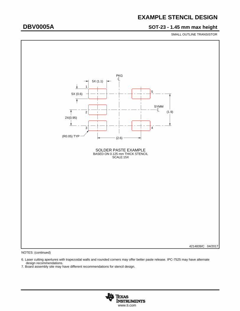
EXAMPLE STENCIL DESIGN
(2.6)
(1.9)
2X(0.95)
5X (1.1)
5X (0.6)
(R0.05) TYP
SOT-23 - 1.45 mm max heightDBV0005ASMALL OUTLINE TRANSISTOR
4214839/C 04/2017
NOTES: (continued) 6. Laser cutting apertures with trapezoidal walls and rounded corners may offer better paste release. IPC-7525 may have alternate design recommendations. 7. Board assembly site may have different recommendations for stencil design.
SOLDER PASTE EXAMPLEBASED ON 0.125 mm THICK STENCIL
SCALE:15X
SYMM
PKG
1
3 4
5
2

www.ti.com
PACKAGE OUTLINE
C
TYP0.220.08
0.25
3.02.6
2X 0.95
1.9
1.45 MAX
TYP0.150.00
5X 0.50.3
TYP0.60.3
TYP80
1.9
A
3.052.75
B1.751.45
(1.1)
SOT-23 - 1.45 mm max heightDBV0005ASMALL OUTLINE TRANSISTOR
4214839/C 04/2017
NOTES: 1. All linear dimensions are in millimeters. Any dimensions in parenthesis are for reference only. Dimensioning and tolerancing per ASME Y14.5M.2. This drawing is subject to change without notice.3. Refernce JEDEC MO-178.
0.2 C A B
1
34
5
2
INDEX AREAPIN 1
GAGE PLANE
SEATING PLANE
0.1 C
SCALE 4.000

www.ti.com
EXAMPLE BOARD LAYOUT
0.07 MAXARROUND
0.07 MINARROUND
5X (1.1)
5X (0.6)
(2.6)
(1.9)
2X (0.95)
(R0.05) TYP
4214839/C 04/2017
SOT-23 - 1.45 mm max heightDBV0005ASMALL OUTLINE TRANSISTOR
NOTES: (continued) 4. Publication IPC-7351 may have alternate designs. 5. Solder mask tolerances between and around signal pads can vary based on board fabrication site.
SYMM
LAND PATTERN EXAMPLEEXPOSED METAL SHOWN
SCALE:15X
PKG
1
3 4
5
2
SOLDER MASKOPENINGMETAL UNDER
SOLDER MASK
SOLDER MASKDEFINED
EXPOSED METAL
METALSOLDER MASKOPENING
NON SOLDER MASKDEFINED
(PREFERRED)
SOLDER MASK DETAILS
EXPOSED METAL

www.ti.com
EXAMPLE STENCIL DESIGN
(2.6)
(1.9)
2X(0.95)
5X (1.1)
5X (0.6)
(R0.05) TYP
SOT-23 - 1.45 mm max heightDBV0005ASMALL OUTLINE TRANSISTOR
4214839/C 04/2017
NOTES: (continued) 6. Laser cutting apertures with trapezoidal walls and rounded corners may offer better paste release. IPC-7525 may have alternate design recommendations. 7. Board assembly site may have different recommendations for stencil design.
SOLDER PASTE EXAMPLEBASED ON 0.125 mm THICK STENCIL
SCALE:15X
SYMM
PKG
1
3 4
5
2

IMPORTANT NOTICE
Texas Instruments Incorporated (TI) reserves the right to make corrections, enhancements, improvements and other changes to itssemiconductor products and services per JESD46, latest issue, and to discontinue any product or service per JESD48, latest issue. Buyersshould obtain the latest relevant information before placing orders and should verify that such information is current and complete.TI’s published terms of sale for semiconductor products (http://www.ti.com/sc/docs/stdterms.htm) apply to the sale of packaged integratedcircuit products that TI has qualified and released to market. Additional terms may apply to the use or sale of other types of TI products andservices.Reproduction of significant portions of TI information in TI data sheets is permissible only if reproduction is without alteration and isaccompanied by all associated warranties, conditions, limitations, and notices. TI is not responsible or liable for such reproduceddocumentation. Information of third parties may be subject to additional restrictions. Resale of TI products or services with statementsdifferent from or beyond the parameters stated by TI for that product or service voids all express and any implied warranties for theassociated TI product or service and is an unfair and deceptive business practice. TI is not responsible or liable for any such statements.Buyers and others who are developing systems that incorporate TI products (collectively, “Designers”) understand and agree that Designersremain responsible for using their independent analysis, evaluation and judgment in designing their applications and that Designers havefull and exclusive responsibility to assure the safety of Designers' applications and compliance of their applications (and of all TI productsused in or for Designers’ applications) with all applicable regulations, laws and other applicable requirements. Designer represents that, withrespect to their applications, Designer has all the necessary expertise to create and implement safeguards that (1) anticipate dangerousconsequences of failures, (2) monitor failures and their consequences, and (3) lessen the likelihood of failures that might cause harm andtake appropriate actions. Designer agrees that prior to using or distributing any applications that include TI products, Designer willthoroughly test such applications and the functionality of such TI products as used in such applications.TI’s provision of technical, application or other design advice, quality characterization, reliability data or other services or information,including, but not limited to, reference designs and materials relating to evaluation modules, (collectively, “TI Resources”) are intended toassist designers who are developing applications that incorporate TI products; by downloading, accessing or using TI Resources in anyway, Designer (individually or, if Designer is acting on behalf of a company, Designer’s company) agrees to use any particular TI Resourcesolely for this purpose and subject to the terms of this Notice.TI’s provision of TI Resources does not expand or otherwise alter TI’s applicable published warranties or warranty disclaimers for TIproducts, and no additional obligations or liabilities arise from TI providing such TI Resources. TI reserves the right to make corrections,enhancements, improvements and other changes to its TI Resources. TI has not conducted any testing other than that specificallydescribed in the published documentation for a particular TI Resource.Designer is authorized to use, copy and modify any individual TI Resource only in connection with the development of applications thatinclude the TI product(s) identified in such TI Resource. NO OTHER LICENSE, EXPRESS OR IMPLIED, BY ESTOPPEL OR OTHERWISETO ANY OTHER TI INTELLECTUAL PROPERTY RIGHT, AND NO LICENSE TO ANY TECHNOLOGY OR INTELLECTUAL PROPERTYRIGHT OF TI OR ANY THIRD PARTY IS GRANTED HEREIN, including but not limited to any patent right, copyright, mask work right, orother intellectual property right relating to any combination, machine, or process in which TI products or services are used. Informationregarding or referencing third-party products or services does not constitute a license to use such products or services, or a warranty orendorsement thereof. Use of TI Resources may require a license from a third party under the patents or other intellectual property of thethird party, or a license from TI under the patents or other intellectual property of TI.TI RESOURCES ARE PROVIDED “AS IS” AND WITH ALL FAULTS. TI DISCLAIMS ALL OTHER WARRANTIES ORREPRESENTATIONS, EXPRESS OR IMPLIED, REGARDING RESOURCES OR USE THEREOF, INCLUDING BUT NOT LIMITED TOACCURACY OR COMPLETENESS, TITLE, ANY EPIDEMIC FAILURE WARRANTY AND ANY IMPLIED WARRANTIES OFMERCHANTABILITY, FITNESS FOR A PARTICULAR PURPOSE, AND NON-INFRINGEMENT OF ANY THIRD PARTY INTELLECTUALPROPERTY RIGHTS. TI SHALL NOT BE LIABLE FOR AND SHALL NOT DEFEND OR INDEMNIFY DESIGNER AGAINST ANY CLAIM,INCLUDING BUT NOT LIMITED TO ANY INFRINGEMENT CLAIM THAT RELATES TO OR IS BASED ON ANY COMBINATION OFPRODUCTS EVEN IF DESCRIBED IN TI RESOURCES OR OTHERWISE. IN NO EVENT SHALL TI BE LIABLE FOR ANY ACTUAL,DIRECT, SPECIAL, COLLATERAL, INDIRECT, PUNITIVE, INCIDENTAL, CONSEQUENTIAL OR EXEMPLARY DAMAGES INCONNECTION WITH OR ARISING OUT OF TI RESOURCES OR USE THEREOF, AND REGARDLESS OF WHETHER TI HAS BEENADVISED OF THE POSSIBILITY OF SUCH DAMAGES.Unless TI has explicitly designated an individual product as meeting the requirements of a particular industry standard (e.g., ISO/TS 16949and ISO 26262), TI is not responsible for any failure to meet such industry standard requirements.Where TI specifically promotes products as facilitating functional safety or as compliant with industry functional safety standards, suchproducts are intended to help enable customers to design and create their own applications that meet applicable functional safety standardsand requirements. Using products in an application does not by itself establish any safety features in the application. Designers mustensure compliance with safety-related requirements and standards applicable to their applications. Designer may not use any TI products inlife-critical medical equipment unless authorized officers of the parties have executed a special contract specifically governing such use.Life-critical medical equipment is medical equipment where failure of such equipment would cause serious bodily injury or death (e.g., lifesupport, pacemakers, defibrillators, heart pumps, neurostimulators, and implantables). Such equipment includes, without limitation, allmedical devices identified by the U.S. Food and Drug Administration as Class III devices and equivalent classifications outside the U.S.TI may expressly designate certain products as completing a particular qualification (e.g., Q100, Military Grade, or Enhanced Product).Designers agree that it has the necessary expertise to select the product with the appropriate qualification designation for their applicationsand that proper product selection is at Designers’ own risk. Designers are solely responsible for compliance with all legal and regulatoryrequirements in connection with such selection.Designer will fully indemnify TI and its representatives against any damages, costs, losses, and/or liabilities arising out of Designer’s non-compliance with the terms and provisions of this Notice.
Mailing Address: Texas Instruments, Post Office Box 655303, Dallas, Texas 75265Copyright © 2018, Texas Instruments Incorporated