Embed Size (px)
Citation preview
MAHARASHTRA STATE BOARD OF TECHNICAL EDUCATION (Autonomous)
(ISO/IEC - 27001 - 2005 Certified)
_____________________________________________________________________________________________
_____
Page 1 of 28
WINTER– 16 EXAMINATION Model Answer Subject Code:
Important Instructions to examiners: 1) The answers should be examined by key words and not as word-to-word as given
in the model answer scheme. 2) The model answer and the answer written by candidate may vary but the examiner
may try to assess the understanding level of the candidate. 3) The language errors such as grammatical, spelling errors should not be given more
Importance (Not applicable for subject English and Communication Skills. 4) While assessing figures, examiner may give credit for principal components
indicated in the figure. The figures drawn by candidate and model answer may vary. The examiner may give credit for any equivalent figure drawn.
5) Credits may be given step wise for numerical problems. In some cases, the assumed constant values may vary and there may be some difference in the candidate’s answers and model answer.
6) In case of some questions credit may be given by judgement on part of examiner of relevant answer based on candidate’s understanding.
7) For programming language papers, credit may be given to any other program based on equivalent concept.
Q.1. a) Answer any SIX of the following: 12
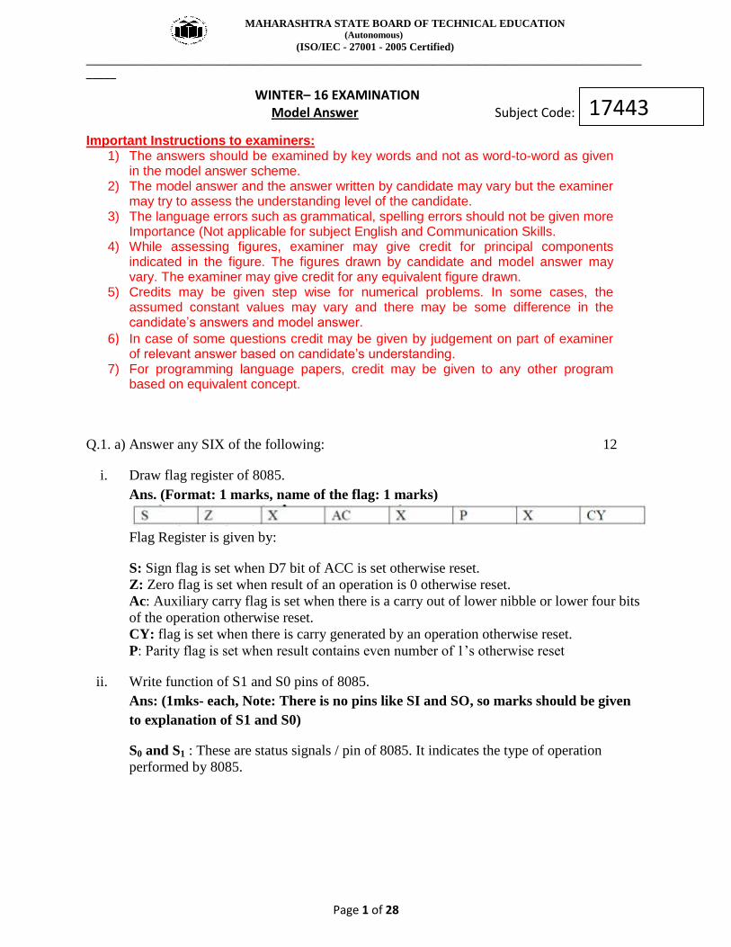
i. Draw flag register of 8085.
Ans. (Format: 1 marks, name of the flag: 1 marks)
Flag Register is given by:
S: Sign flag is set when D7 bit of ACC is set otherwise reset.
Z: Zero flag is set when result of an operation is 0 otherwise reset.
Ac: Auxiliary carry flag is set when there is a carry out of lower nibble or lower four bits
of the operation otherwise reset.
CY: flag is set when there is carry generated by an operation otherwise reset.
P: Parity flag is set when result contains even number of 1’s otherwise reset
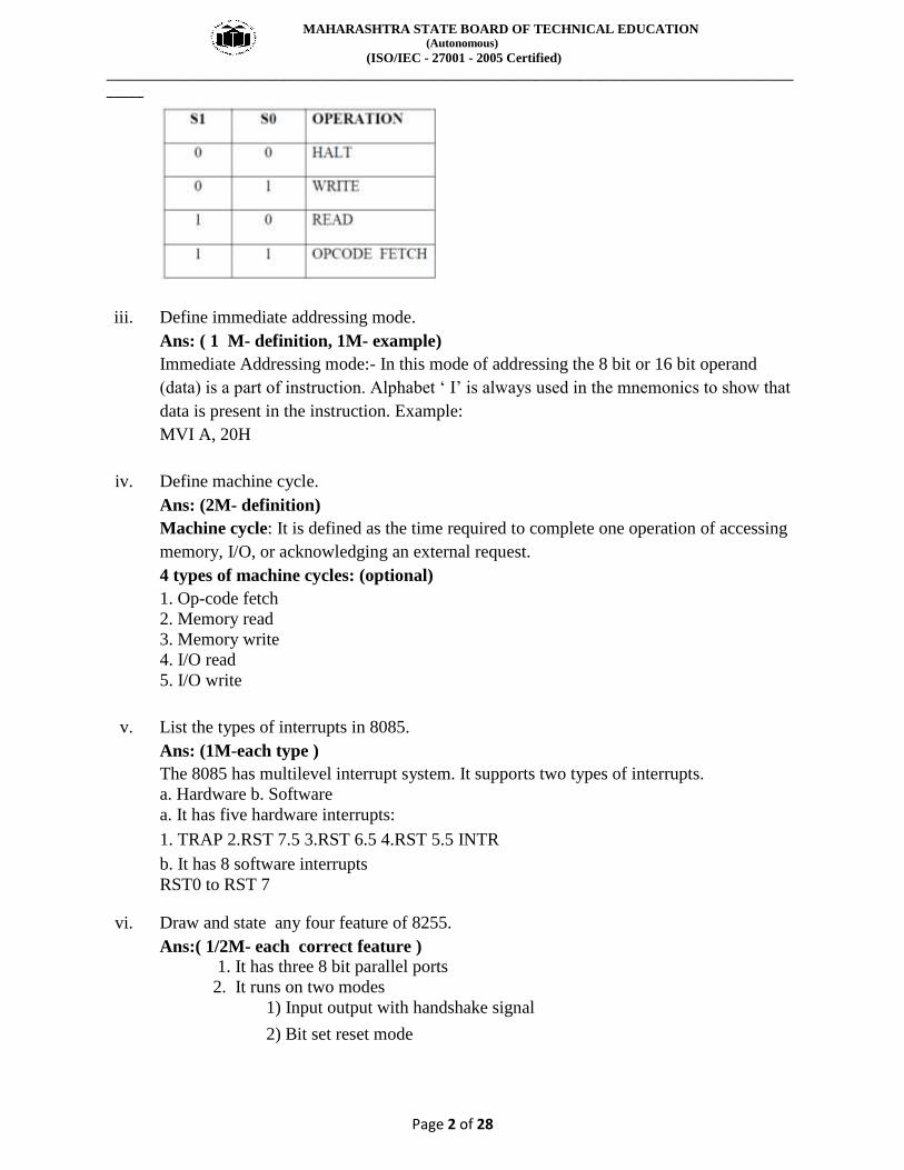
ii. Write function of S1 and S0 pins of 8085.
Ans: (1mks- each, Note: There is no pins like SI and SO, so marks should be given
to explanation of S1 and S0)
S0 and S1 : These are status signals / pin of 8085. It indicates the type of operation
performed by 8085.
17443
MAHARASHTRA STATE BOARD OF TECHNICAL EDUCATION (Autonomous)
(ISO/IEC - 27001 - 2005 Certified)
_____________________________________________________________________________________________
_____
Page 2 of 28
iii. Define immediate addressing mode.
Ans: ( 1 M- definition, 1M- example)
Immediate Addressing mode:- In this mode of addressing the 8 bit or 16 bit operand
(data) is a part of instruction. Alphabet ‘ I’ is always used in the mnemonics to show that
data is present in the instruction. Example:
MVI A, 20H
iv. Define machine cycle.
Ans: (2M- definition)
Machine cycle: It is defined as the time required to complete one operation of accessing
memory, I/O, or acknowledging an external request.
4 types of machine cycles: (optional)
1. Op-code fetch
2. Memory read
3. Memory write
4. I/O read
5. I/O write
v. List the types of interrupts in 8085.
Ans: (1M-each type )
The 8085 has multilevel interrupt system. It supports two types of interrupts.
a. Hardware b. Software
a. It has five hardware interrupts:
1. TRAP 2.RST 7.5 3.RST 6.5 4.RST 5.5 INTR
b. It has 8 software interrupts
RST0 to RST 7
vi. Draw and state any four feature of 8255.
Ans:( 1/2M- each correct feature ) 1. It has three 8 bit parallel ports
2. It runs on two modes
1) Input output with handshake signal
2) Bit set reset mode
MAHARASHTRA STATE BOARD OF TECHNICAL EDUCATION (Autonomous)
(ISO/IEC - 27001 - 2005 Certified)
_____________________________________________________________________________________________
_____
Page 3 of 28
3. It requires +5V power supply
4. Fully TTL compatible
5. Direct bit set reset capability is available with Port C.
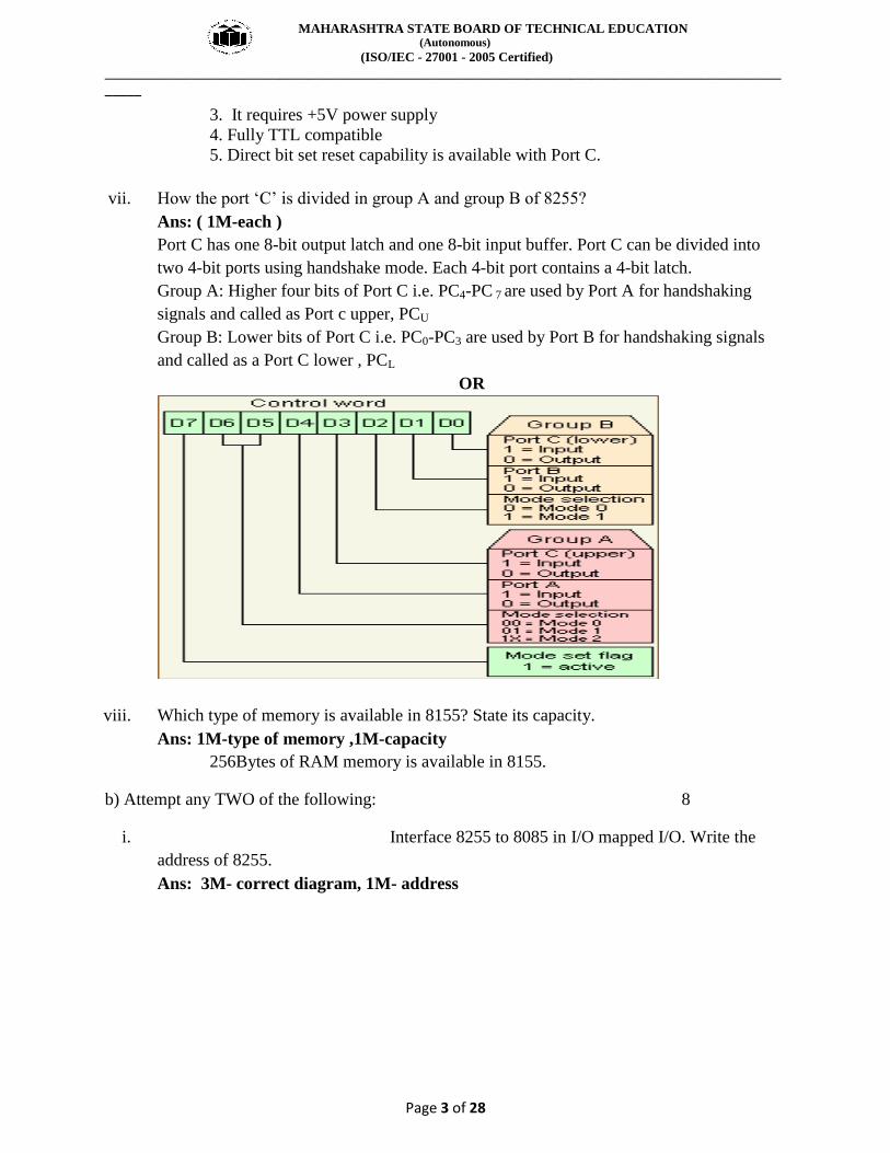
vii. How the port ‘C’ is divided in group A and group B of 8255?
Ans: ( 1M-each )
Port C has one 8-bit output latch and one 8-bit input buffer. Port C can be divided into
two 4-bit ports using handshake mode. Each 4-bit port contains a 4-bit latch.
Group A: Higher four bits of Port C i.e. PC4-PC 7 are used by Port A for handshaking
signals and called as Port c upper, PCU
Group B: Lower bits of Port C i.e. PC0-PC3 are used by Port B for handshaking signals
and called as a Port C lower , PCL
OR
viii. Which type of memory is available in 8155? State its capacity.
Ans: 1M-type of memory ,1M-capacity
256Bytes of RAM memory is available in 8155.
b) Attempt any TWO of the following: 8
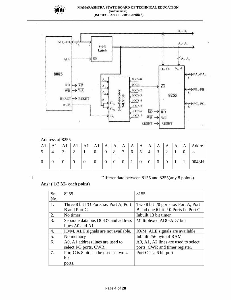
i. Interface 8255 to 8085 in I/O mapped I/O. Write the
address of 8255.
Ans: 3M- correct diagram, 1M- address
MAHARASHTRA STATE BOARD OF TECHNICAL EDUCATION (Autonomous)
(ISO/IEC - 27001 - 2005 Certified)
_____________________________________________________________________________________________
_____
Page 4 of 28
Address of 8255
A1
5
A1
4
A1
3
A1
2
A1
1
A1
0
A
9
A
8
A
7
A
6
A
5
A
4
A
3
A
2
A
1
A
0
Addre
ss
0 0 0 0 0 0 0 0 0 1 0 0 0 0 1 1 0043H
ii. Differentiate between 8155 and 8255(any 8 points)
Ans: ( 1/2 M– each point)
Sr.
No.
8255 8155
1. Three 8 bit I/O Ports i.e. Port A, Port
B and Port C
Two 8 bit I/0 ports i.e. Port A, Port
B and one 6 bit I/ 0 Ports i.e.Port C
2. No timer Inbuilt 13 bit timer
3. Separate data bus D0-D7 and address
lines A0 and A1
Multiplexed AD0-AD7 bus
4. IO/M, ALE signals are not available. IO/M, ALE signals are available
5. No memory Inbuilt 256 byte of RAM
6. A0, A1 address lines are used to
select I/O ports, CWR.
A0, A1, A2 lines are used to select
ports, CWR and timer register.
7. Port C is 8 bit can be used as two 4
bit
ports.
Port C is a 6 bit port
MAHARASHTRA STATE BOARD OF TECHNICAL EDUCATION (Autonomous)
(ISO/IEC - 27001 - 2005 Certified)
_____________________________________________________________________________________________
_____
Page 5 of 28
8. Bit set reset facility is available with
port C
Bit set reset facility is not available
with port C
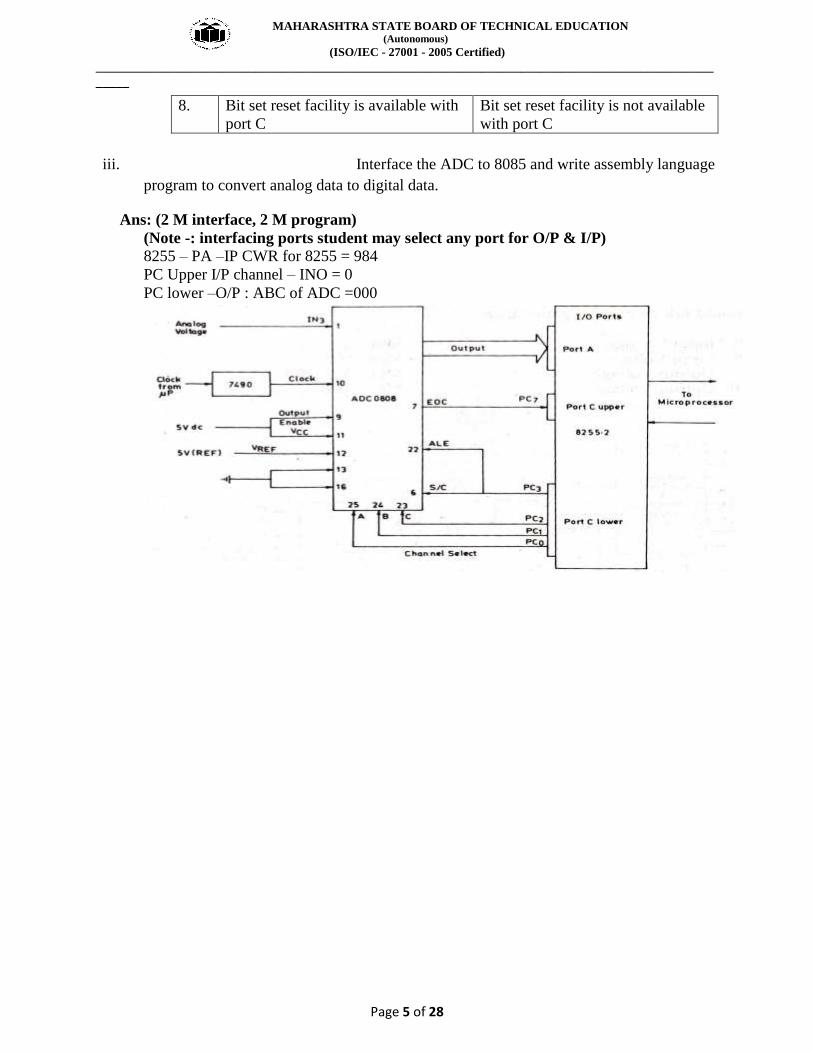
iii. Interface the ADC to 8085 and write assembly language
program to convert analog data to digital data.
Ans: (2 M interface, 2 M program)
(Note -: interfacing ports student may select any port for O/P & I/P) 8255 – PA –IP CWR for 8255 = 984
PC Upper I/P channel – INO = 0
PC lower –O/P : ABC of ADC =000
MAHARASHTRA STATE BOARD OF TECHNICAL EDUCATION (Autonomous)
(ISO/IEC - 27001 - 2005 Certified)
_____________________________________________________________________________________________
_____
Page 6 of 28
Q.2 Attempt any FOUR of the following: 16
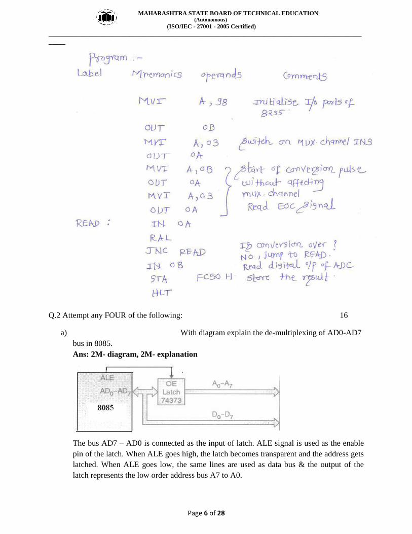
a) With diagram explain the de-multiplexing of AD0-AD7
bus in 8085.
Ans: 2M- diagram, 2M- explanation
The bus AD7 – AD0 is connected as the input of latch. ALE signal is used as the enable
pin of the latch. When ALE goes high, the latch becomes transparent and the address gets
latched. When ALE goes low, the same lines are used as data bus & the output of the
latch represents the low order address bus A7 to A0.
MAHARASHTRA STATE BOARD OF TECHNICAL EDUCATION (Autonomous)
(ISO/IEC - 27001 - 2005 Certified)
_____________________________________________________________________________________________
_____
Page 7 of 28
b) With examples describe any two addressing modes of
8085.
Ans:- ( any 2 addressing modes ,2 mark each.)
Note: any valid example can be considered
1) Immediate Addressing mode:- In this mode of addressing the 8 bit or 16 bit
operand (data) is a part of instruction .
MVI A,20H
2) Register Addressing mode:- In this mode of addressing the operand (data) is in one of
the general purpose register or accumulator.
MOV B, A
3) Direct Addressing mode:- In this mode of addressing the address of operand (data) is a
part of instruction.
LDA 6020H
4) Indirect Addressing mode:- In this mode of addressing the address of the operand
(data) is specified by a register pair.
MOV B, M .
5) Implicit / Implied Addressing mode:- In this mode of addressing the operand (data) is
in accumulator.
RAR
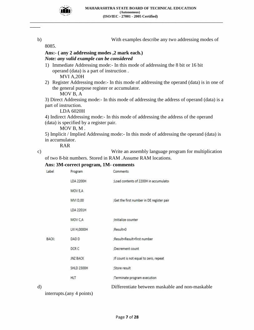
c) Write an assembly language program for multiplication
of two 8-bit numbers. Stored in RAM .Assume RAM locations.
Ans: 3M-correct program, 1M- comments
d) Differentiate between maskable and non-maskable
interrupts.(any 4 points)
MAHARASHTRA STATE BOARD OF TECHNICAL EDUCATION (Autonomous)
(ISO/IEC - 27001 - 2005 Certified)
_____________________________________________________________________________________________
_____
Page 8 of 28
Ans: 1M-each point
Sr.no Maskable interrupt Non-maskable interrupt
1 It can be disabled or ignored by
the instructions of CPU
It cannot be disabled or ignored by
the instructions of CPU
2 These are the interrupts generally
coming from the peripheral
devices.
Generally occurs due to signal
attention for non –recoverable
hardware errors which needs
immediate attention.
3 EI and DI instructions can be used
for enabling and disabling
interrupts.
EI and DI instructions cannot be
used for enabling and disabling
interrupts.
4 Examples are RST 5.5,RST 6.5,
RST 7.5
Example is TRAP
e) How SOD and SID pins can be used as a single bit
output and input ports respectively?
Ans. (SOD pin: 2 marks, SID pin: 2 marks) SOD (Serial Output data): When SIM instruction is executed, the content of MSB of
accumulator is transferred to SOD pin. The instruction SIM is necessary to output data
serially from the SOD line. It can be interpreted for serial output.
INSTRUCTIONS:
MVI A,80H ;Set D7 in the accumulator = 1
RAR ;Set D6 = 1 and bring Carry into D7
SIM ;Output D7
SID (Serial Input data): When RIM instruction is executed, the content of SID pin is
loaded into MSB of Accumulator. Instruction RIM is used to input serial data through the
SID line. Instruction RIM can be interpreted for serial I/O. In the context of serial I/O,
instruction RIM is similar to instruction IN, except RIM reads only one bit and places it
in the accumulator at D7.
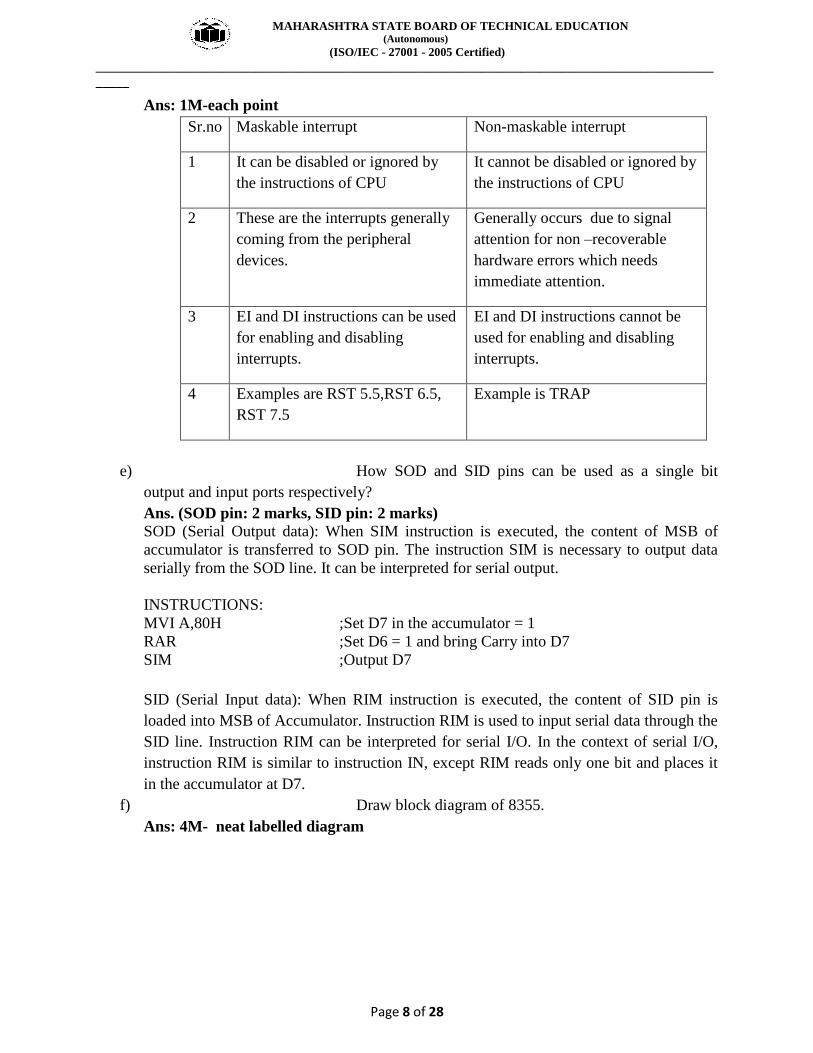
f) Draw block diagram of 8355.
Ans: 4M- neat labelled diagram
MAHARASHTRA STATE BOARD OF TECHNICAL EDUCATION (Autonomous)
(ISO/IEC - 27001 - 2005 Certified)
_____________________________________________________________________________________________
_____
Page 9 of 28
Q3. Attempt any FOUR of the following:
a) Write salient features of 8085.(any eight)
Ans: (any 8 features, each feature ½ M) 1. It is an 8 bit processor.
2. It is a single chip N-MOS device with 40 pins.
3. It has multiplexed address and data bus.(AD0-AD7).
4. It works on 5 Volt dc power supply.
5. The maximum clock frequency is 3 MHz while minimum frequency is 500kHz.
6. It provides 74 instructions with 5 different addressing modes.
7. It provides 16 address lines so it can access 2^16 =64K bytes of memory.
8. It generates 8 bit I/O address so it can access 2^8=256 input ports.
9. It provides 5 hardware interrupts: TRAP, RST 5.5, RST 6.5, RST 7.5,INTR.
10. It provides ACC ,one flag register ,6 general purpose registers and two special purpose
registers(SP,PC).
11. It provides serial lines SID , SOD. So serial peripherals can be interfaced with 8085
directly.
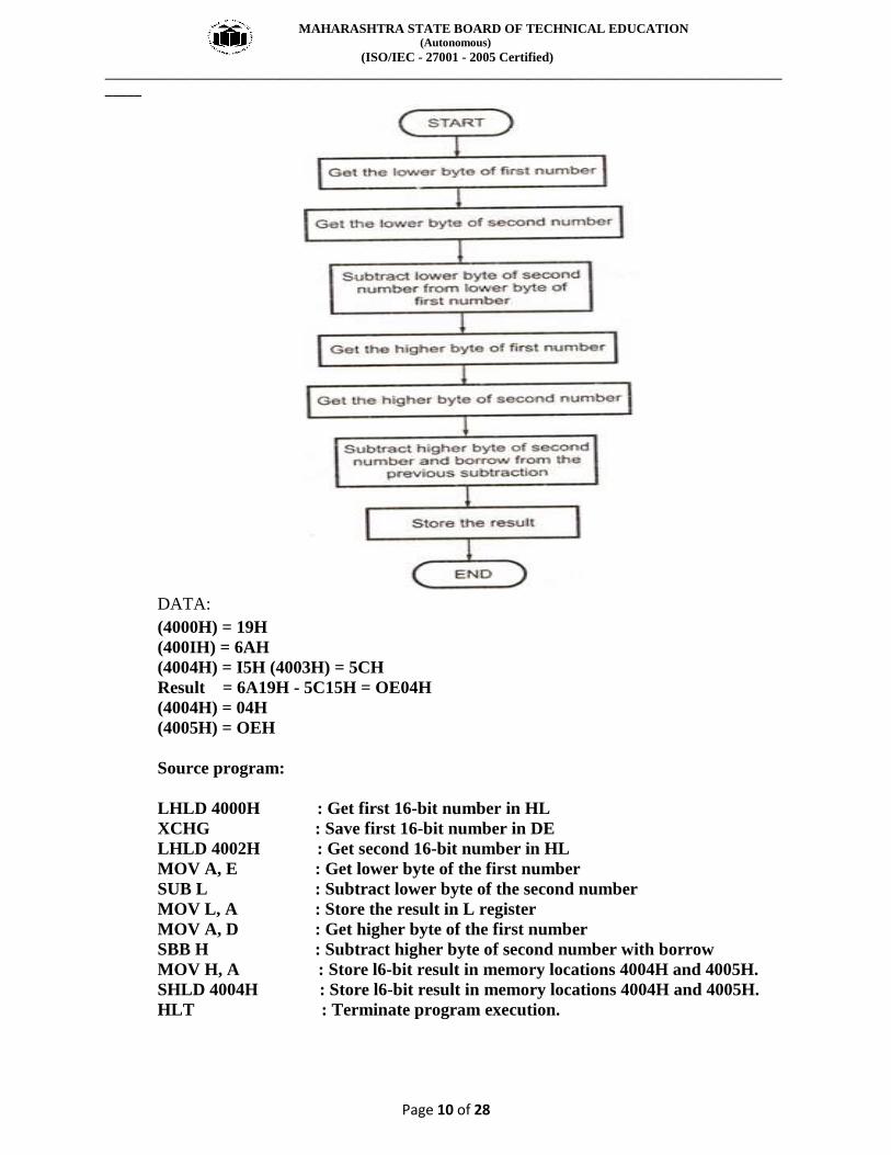
b) Draw flowchart and write a program for subtraction of
two 16-bit numbers stored in memory.(Assume suitable memory location)
Ans: Flowchart-2M, Prog- 2M
MAHARASHTRA STATE BOARD OF TECHNICAL EDUCATION (Autonomous)
(ISO/IEC - 27001 - 2005 Certified)
_____________________________________________________________________________________________
_____
Page 10 of 28
DATA:
(4000H) = 19H
(400IH) = 6AH
(4004H) = I5H (4003H) = 5CH
Result = 6A19H - 5C15H = OE04H
(4004H) = 04H
(4005H) = OEH
Source program:
LHLD 4000H : Get first 16-bit number in HL
XCHG : Save first 16-bit number in DE
LHLD 4002H : Get second 16-bit number in HL
MOV A, E : Get lower byte of the first number
SUB L : Subtract lower byte of the second number
MOV L, A : Store the result in L register
MOV A, D : Get higher byte of the first number
SBB H : Subtract higher byte of second number with borrow
MOV H, A : Store l6-bit result in memory locations 4004H and 4005H.
SHLD 4004H : Store l6-bit result in memory locations 4004H and 4005H.
HLT : Terminate program execution.
MAHARASHTRA STATE BOARD OF TECHNICAL EDUCATION (Autonomous)
(ISO/IEC - 27001 - 2005 Certified)
_____________________________________________________________________________________________
_____
Page 11 of 28
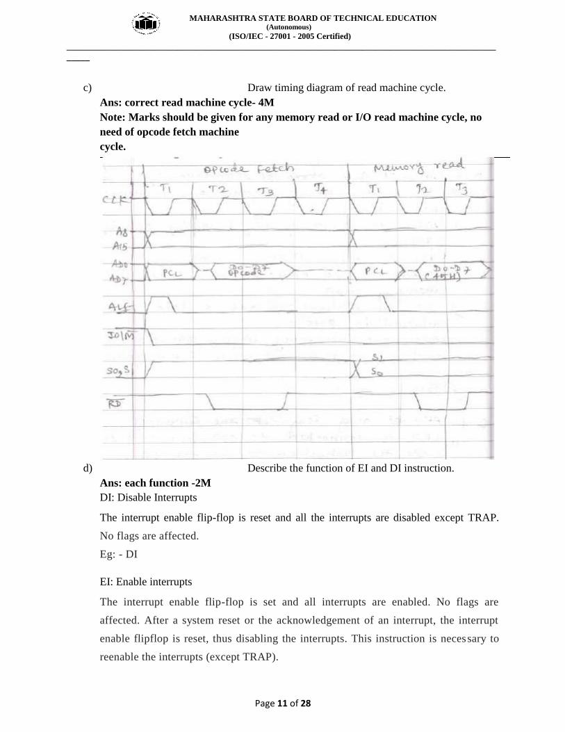
c) Draw timing diagram of read machine cycle.
Ans: correct read machine cycle- 4M
Note: Marks should be given for any memory read or I/O read machine cycle, no
need of opcode fetch machine
cycle.
d) Describe the function of EI and DI instruction.
Ans: each function -2M
DI: Disable Interrupts
The interrupt enable flip-flop is reset and all the interrupts are disabled except TRAP.
No flags are affected.
Eg: - DI
EI: Enable interrupts
The interrupt enable flip-flop is set and all interrupts are enabled. No flags are
affected. After a system reset or the acknowledgement of an interrupt, the interrupt
enable flipflop is reset, thus disabling the interrupts. This instruction is necessary to
reenable the interrupts (except TRAP).
MAHARASHTRA STATE BOARD OF TECHNICAL EDUCATION (Autonomous)
(ISO/IEC - 27001 - 2005 Certified)
_____________________________________________________________________________________________
_____
Page 12 of 28
Eg: - EI
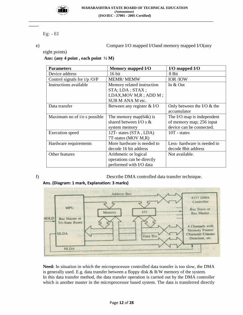
e) Compare I/O mapped I/Oand memory mapped I/O(any
eight points)
Ans: (any 4 point , each point ½ M)
Parameters Memory mapped I/O I/O mapped I/O
Device address 16 bit 8 Bit
Control signals for i/p /O/P MEMR/ MEMW IOR /IOW
Instructions available Memory related instruction
STA; LDA ; STAX ;
LDAX,MOV M,R ; ADD M ;
SUB M ANA M etc.
In & Out
Data transfer Between any register & I/O Only between the I/O & the
accumulator
Maximum no of i/o s possible The memory map(64k) is
shared between I/O s &
system memory
The I/O map is independent
of memory map; 256 input
device can be connected.
Execution speed 12T- states (STA , LDA)
7T-states (MOV M,R)
10T - states
Hardware requirements More hardware is needed to
decode 16 bit address
Less- hardware is needed to
decode 8bit address
Other features Arithmetic or logical
operations can be directly
performed with I/O data
Not available.
f) Describe DMA controlled data transfer technique.
Ans. (Diagram: 1 mark, Explanation: 3 marks)
Need: In situation in which the microprocessor controlled data transfer is too slow, the DMA
is generally used. E.g. data transfer between a floppy disk & R/W memory of the system.
In this data transfer method, the data transfer operation is carried out by the DMA controller
which is another master in the microprocessor based system. The data is transferred directly
MAHARASHTRA STATE BOARD OF TECHNICAL EDUCATION (Autonomous)
(ISO/IEC - 27001 - 2005 Certified)
_____________________________________________________________________________________________
_____
Page 13 of 28
between I/O device and memory and data transfer is controlled by either I/O device or DMA
controller. Microprocessor does not participate in this data transfer method. Whenever there
is request from the I/O device, then DMA controller takes the control of all system buses i.e.
address bus, data bus and control bus and perform data transfer operation directly between
I/O device and memory. This method is used when the large amount of data is required to be
transfer.
In IBM PC, Hard disk drive, floppy disk drive CD- ROM etc. devices uses this method of
data transfer. In this method, when an I/O device wishes for data transfer, an I/O device itself
generate request signal DREQ to DMA controller. In response to DREQ, the DMA controller
send HOLD signal to the microprocessor. After receiving HOLD signal, microprocessor
performs current operation completely and transfer the control of all system buses i.e.address
bus, data bus and control bus to DMA controller. The DMA controller start data transfer
operation. The speed of the data transfer is faster as compare to programmed I/O data transfer
method. The three data transfer schemes of DMA are as given below:
1. Single Byte Transfer: Only one byte data is transferred at a time – data transfer speed is
low. In this mode of DMA data transfer, only one byte of data is transferred at a time, hence
the data transfer speed is slow. DMA controller send HOLD signal to microprocessor and
wait for HLDA (Acknowledge) signal. After receiving HLDA signal from microprocessor,
the DMA enter into master mode and gain the control of all system buses and execute only
one DMA cycle to transfer one byte of data. After transferring one byte of data, the DMA
controller disable HOLD signal, enter into slave mode and transfer the control of system
buses to the microprocessor. This process is repeated to transfer all data bytes. Means, the
DMA controller enables and disable HOLD signal for all data bytes transfer
2. Block Transfer: In this mode of DMA data transfer, the block of data bytes is transferred
continuously. During the DMA data transfer, the microprocessor is disconnected from the
system buses, hence the microprocessor cannot executes its own programs. N number of
DMA cycle are added into the machine cycle of the microprocessor where N indicates
numbers of bytes to be transferred .In this mode, the DMA controller sends HOLD signal to
the microprocessor to gain the control of the system buses and wait for HLDA signal. After
receiving HLDA signal, the DMA controller enters into the master mode and starts data
transfer operation. After transferring all data bytes of the block, the DMA controller disable
HOLD signal and enter into the slave mode. This mode DMA data transfer is faster than
single byte mode.
3. Hidden or Transparent DMA: In the machine cycle of microprocessor, there are some
states during which all buses are not used by the microprocessor means it floats system buses.
During these states, the microprocessor is isolated from the system buses and DMA
controller transfer data between I/O device and memory. This is slowest DMA data transfer.
In this method, additional logic i.e. hardware is required to detect the idle states when the
microprocessor floats its buses.
Q.4 Attempt any FOUR of the following:
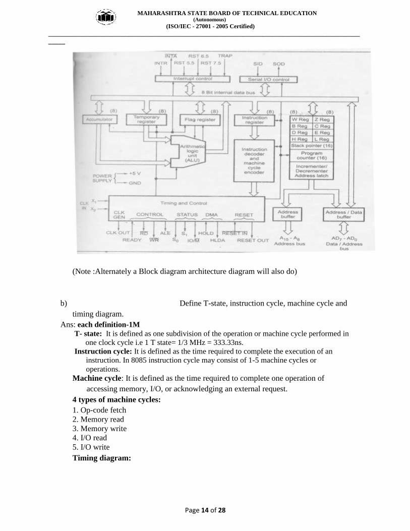
a) Draw a neat labelled internal architecture of 8085.
Ans: diagram-4M)
MAHARASHTRA STATE BOARD OF TECHNICAL EDUCATION (Autonomous)
(ISO/IEC - 27001 - 2005 Certified)
_____________________________________________________________________________________________
_____
Page 14 of 28
(Note :Alternately a Block diagram architecture diagram will also do)
b) Define T-state, instruction cycle, machine cycle and
timing diagram.
Ans: each definition-1M
T- state: It is defined as one subdivision of the operation or machine cycle performed in
one clock cycle i.e 1 T state= 1/3 MHz = 333.33ns. Instruction cycle: It is defined as the time required to complete the execution of an
instruction. In 8085 instruction cycle may consist of 1-5 machine cycles or
operations.
Machine cycle: It is defined as the time required to complete one operation of
accessing memory, I/O, or acknowledging an external request.
4 types of machine cycles:
1. Op-code fetch
2. Memory read
3. Memory write
4. I/O read
5. I/O write
Timing diagram:
MAHARASHTRA STATE BOARD OF TECHNICAL EDUCATION (Autonomous)
(ISO/IEC - 27001 - 2005 Certified)
_____________________________________________________________________________________________
_____
Page 15 of 28
It is the graphical representation of process in steps with respect to time. The timing
diagram represents the clock cycle and duration, delay, content of address bus and data
bus, type of operation ie. Read/write/status signals from memory or I/O.
c) Explain any four arithmetic instructions by giving
examples of each.
Ans: any 4 correct instructions – 1M each
DAD Reg.
pair
Add the register
pair to H and L
registers
The 16-bit data of the
specified register pair are
added to the contents of the
HL register.
Example − DAD B
SUB R/M
Subtract the
register or the
memory from the
accumulator
The contents of the register
or the memory are
subtracted from the contents
of the accumulator, and the
result is stored in the
accumulator.
Example − SUB D
DAA None Decimal adjust
accumulator
The contents of the accumulator
are changed from a binary value
to two 4-bit BCD digits.
If the value of the low-order 4-
bits in the accumulator is
greater than 9 or if AC flag is
set, the instruction adds 6 to the
low-order four bits.
If the value of the high-order 4-
bits in the accumulator is
greater than 9 or if the Carry
MAHARASHTRA STATE BOARD OF TECHNICAL EDUCATION (Autonomous)
(ISO/IEC - 27001 - 2005 Certified)
_____________________________________________________________________________________________
_____
Page 16 of 28
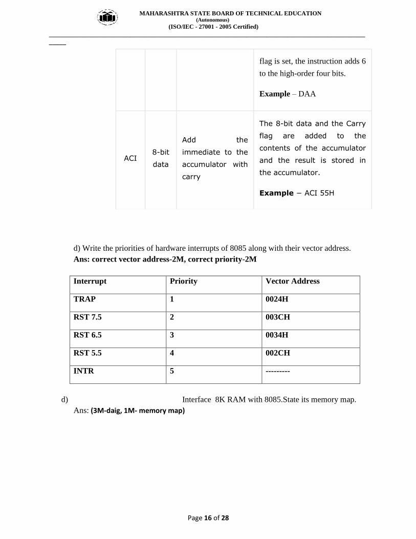
d) Write the priorities of hardware interrupts of 8085 along with their vector address.
Ans: correct vector address-2M, correct priority-2M
Interrupt Priority Vector Address
TRAP 1 0024H
RST 7.5 2 003CH
RST 6.5 3 0034H
RST 5.5 4 002CH
INTR 5 ---------
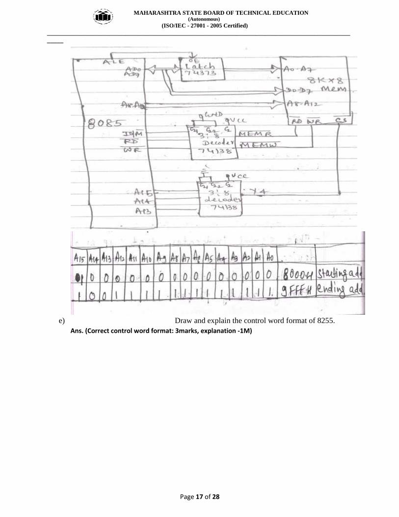
d) Interface 8K RAM with 8085.State its memory map.
Ans: (3M-daig, 1M- memory map)
flag is set, the instruction adds 6
to the high-order four bits.
Example – DAA
ACI 8-bit
data
Add the
immediate to the
accumulator with
carry
The 8-bit data and the Carry
flag are added to the
contents of the accumulator
and the result is stored in
the accumulator.
Example − ACI 55H
MAHARASHTRA STATE BOARD OF TECHNICAL EDUCATION (Autonomous)
(ISO/IEC - 27001 - 2005 Certified)
_____________________________________________________________________________________________
_____
Page 17 of 28
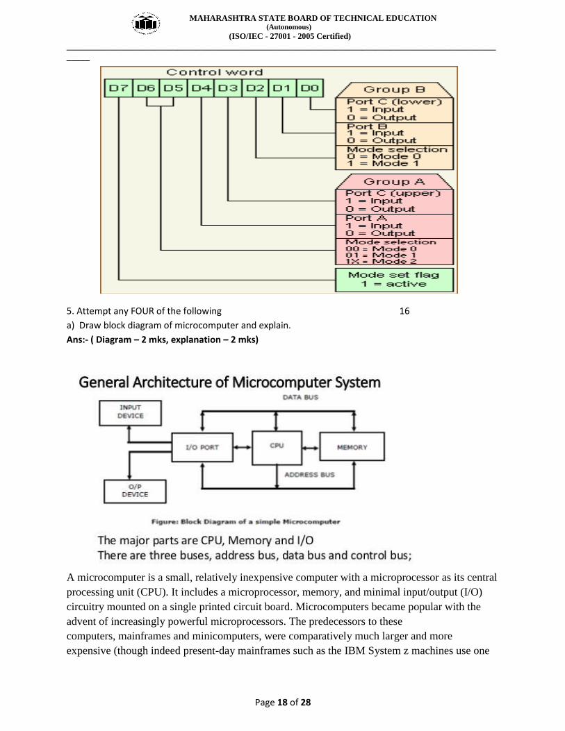
e) Draw and explain the control word format of 8255.
Ans. (Correct control word format: 3marks, explanation -1M)
MAHARASHTRA STATE BOARD OF TECHNICAL EDUCATION (Autonomous)
(ISO/IEC - 27001 - 2005 Certified)
_____________________________________________________________________________________________
_____
Page 18 of 28
5. Attempt any FOUR of the following 16
a) Draw block diagram of microcomputer and explain.
Ans:- ( Diagram – 2 mks, explanation – 2 mks)
A microcomputer is a small, relatively inexpensive computer with a microprocessor as its central
processing unit (CPU). It includes a microprocessor, memory, and minimal input/output (I/O)
circuitry mounted on a single printed circuit board. Microcomputers became popular with the
advent of increasingly powerful microprocessors. The predecessors to these
computers, mainframes and minicomputers, were comparatively much larger and more
expensive (though indeed present-day mainframes such as the IBM System z machines use one
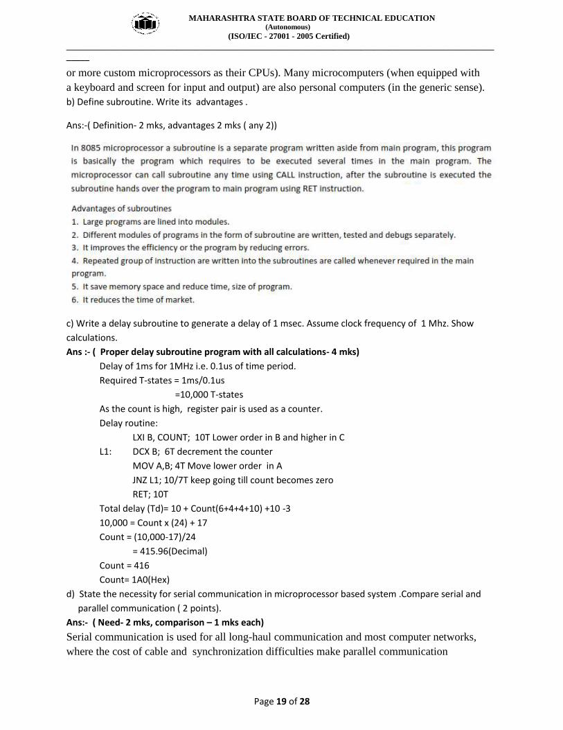
MAHARASHTRA STATE BOARD OF TECHNICAL EDUCATION (Autonomous)
(ISO/IEC - 27001 - 2005 Certified)
_____________________________________________________________________________________________
_____
Page 19 of 28
or more custom microprocessors as their CPUs). Many microcomputers (when equipped with
a keyboard and screen for input and output) are also personal computers (in the generic sense).
b) Define subroutine. Write its advantages .
Ans:-( Definition- 2 mks, advantages 2 mks ( any 2))
c) Write a delay subroutine to generate a delay of 1 msec. Assume clock frequency of 1 Mhz. Show
calculations.
Ans :- ( Proper delay subroutine program with all calculations- 4 mks)
Delay of 1ms for 1MHz i.e. 0.1us of time period.
Required T-states = 1ms/0.1us
=10,000 T-states
As the count is high, register pair is used as a counter.
Delay routine:
LXI B, COUNT; 10T Lower order in B and higher in C
L1: DCX B; 6T decrement the counter
MOV A,B; 4T Move lower order in A
JNZ L1; 10/7T keep going till count becomes zero
RET; 10T
Total delay (Td)= 10 + Count(6+4+4+10) +10 -3
10,000 = Count x (24) + 17
Count = (10,000-17)/24
= 415.96(Decimal)
Count = 416
Count= 1A0(Hex)
d) State the necessity for serial communication in microprocessor based system .Compare serial and
parallel communication ( 2 points).
Ans:- ( Need- 2 mks, comparison – 1 mks each)
Serial communication is used for all long-haul communication and most computer networks,
where the cost of cable and synchronization difficulties make parallel communication
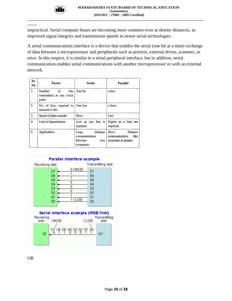
MAHARASHTRA STATE BOARD OF TECHNICAL EDUCATION (Autonomous)
(ISO/IEC - 27001 - 2005 Certified)
_____________________________________________________________________________________________
_____
Page 20 of 28
impractical. Serial computer buses are becoming more common even at shorter distances, as
improved signal integrity and transmission speeds in newer serial technologies .
A serial communications interface is a device that enables the serial (one bit at a time) exchange
of data between a microprocessor and peripherals such as printers, external drives, scanners, or
mice. In this respect, it is similar to a serial peripheral interface, but in addition, serial
communication enables serial communications with another microprocessor or with an external
network.
OR
MAHARASHTRA STATE BOARD OF TECHNICAL EDUCATION (Autonomous)
(ISO/IEC - 27001 - 2005 Certified)
_____________________________________________________________________________________________
_____
Page 21 of 28
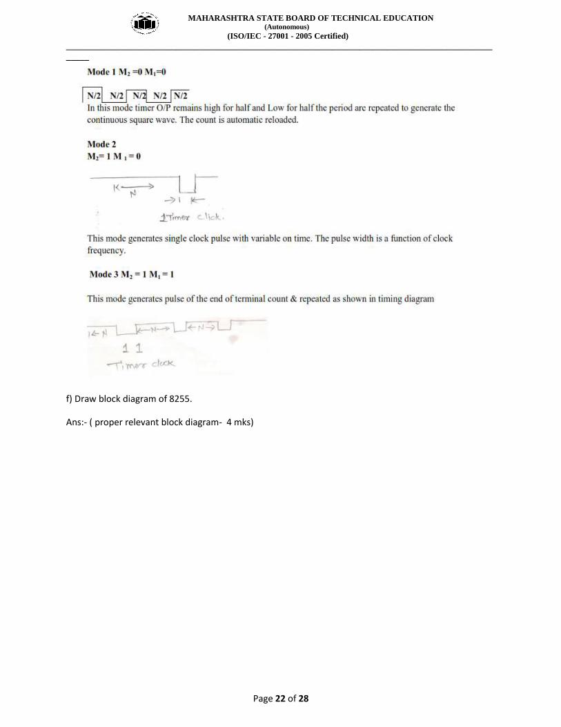
e) Write the timer modes of 8155 and explain any one with timing diagram.
Ans:- ( Modes - 2 mks ( any four). Any one explanation- 2 mks)
MAHARASHTRA STATE BOARD OF TECHNICAL EDUCATION (Autonomous)
(ISO/IEC - 27001 - 2005 Certified)
_____________________________________________________________________________________________
_____
Page 22 of 28
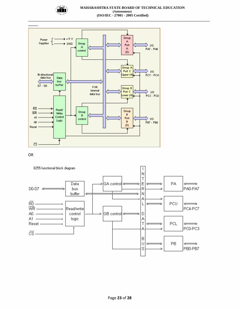
f) Draw block diagram of 8255.
Ans:- ( proper relevant block diagram- 4 mks)
MAHARASHTRA STATE BOARD OF TECHNICAL EDUCATION (Autonomous)
(ISO/IEC - 27001 - 2005 Certified)
_____________________________________________________________________________________________
_____
Page 23 of 28
OR
MAHARASHTRA STATE BOARD OF TECHNICAL EDUCATION (Autonomous)
(ISO/IEC - 27001 - 2005 Certified)
_____________________________________________________________________________________________
_____
Page 24 of 28
6. Attempt any FOUR of the following 16
a) Describe the following blocks of 8085.
i) ALU ii) Timing and control unit
Ans:- ( Each description- 2 mks)
b) Write assembly language program to calculate the sum of 10 numbers stored in RAM. Store the result
in RAM . Assume RAM locations.
Ans:- ( Proper relevant program- 3M,comments-1M)
;; HL points to array of bytes to be added ;; DE contains 16-bit sum ;; C is loop counter
LXI H, 4500H ; point to first byte MOV E, M ; fetch first byte MVI D, 0 ; clear high byte of sum MVI C, 10 ; add 10 more bytes loop: INX H ; point to next byte MOV A, M ; fetch next byte ADD E ; add to sum MOV E, A JNC SKIP ; if carry ... INR D ; increment high byte of sum skip: DCR C ; decrement loop counter JNZ LOOP ; repeat if not done ;; Store the result XCHG ; move sum to HL SHLD 3000H HLT
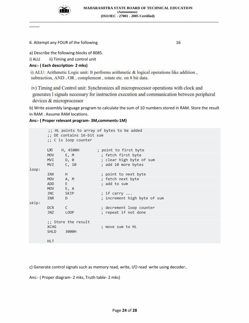
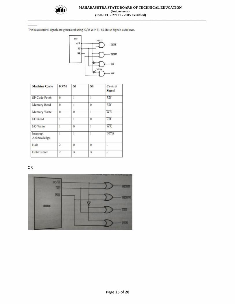
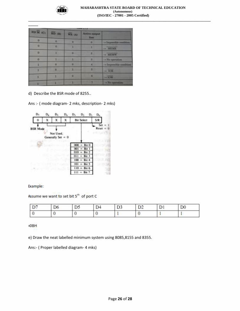
c) Generate control signals such as memory read, write, I/O read write using decoder..
Ans:- ( Proper diagram- 2 mks, Truth table- 2 mks)
MAHARASHTRA STATE BOARD OF TECHNICAL EDUCATION (Autonomous)
(ISO/IEC - 27001 - 2005 Certified)
_____________________________________________________________________________________________
_____
Page 25 of 28
OR
MAHARASHTRA STATE BOARD OF TECHNICAL EDUCATION (Autonomous)
(ISO/IEC - 27001 - 2005 Certified)
_____________________________________________________________________________________________
_____
Page 26 of 28
d) Describe the BSR mode of 8255..
Ans :- ( mode diagram- 2 mks, description- 2 mks)
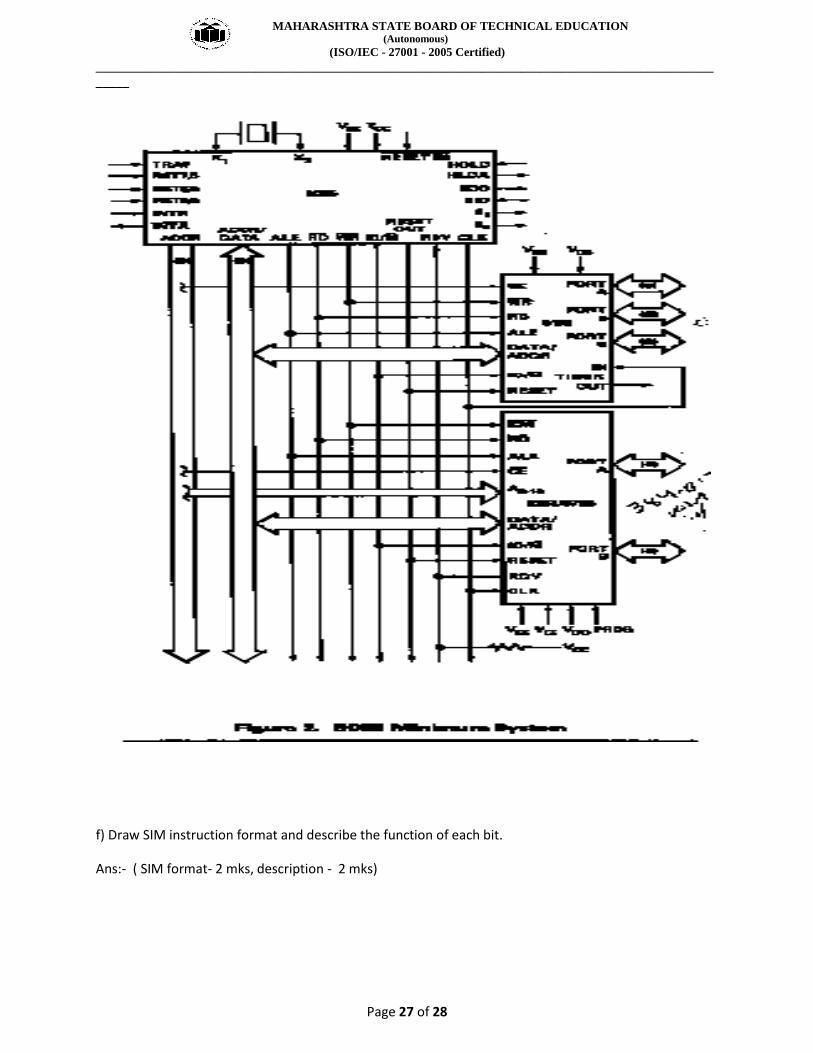
e) Draw the neat labelled minimum system using 8085,8155 and 8355.
Ans:- ( Proper labelled diagram- 4 mks)
MAHARASHTRA STATE BOARD OF TECHNICAL EDUCATION (Autonomous)
(ISO/IEC - 27001 - 2005 Certified)
_____________________________________________________________________________________________
_____
Page 27 of 28
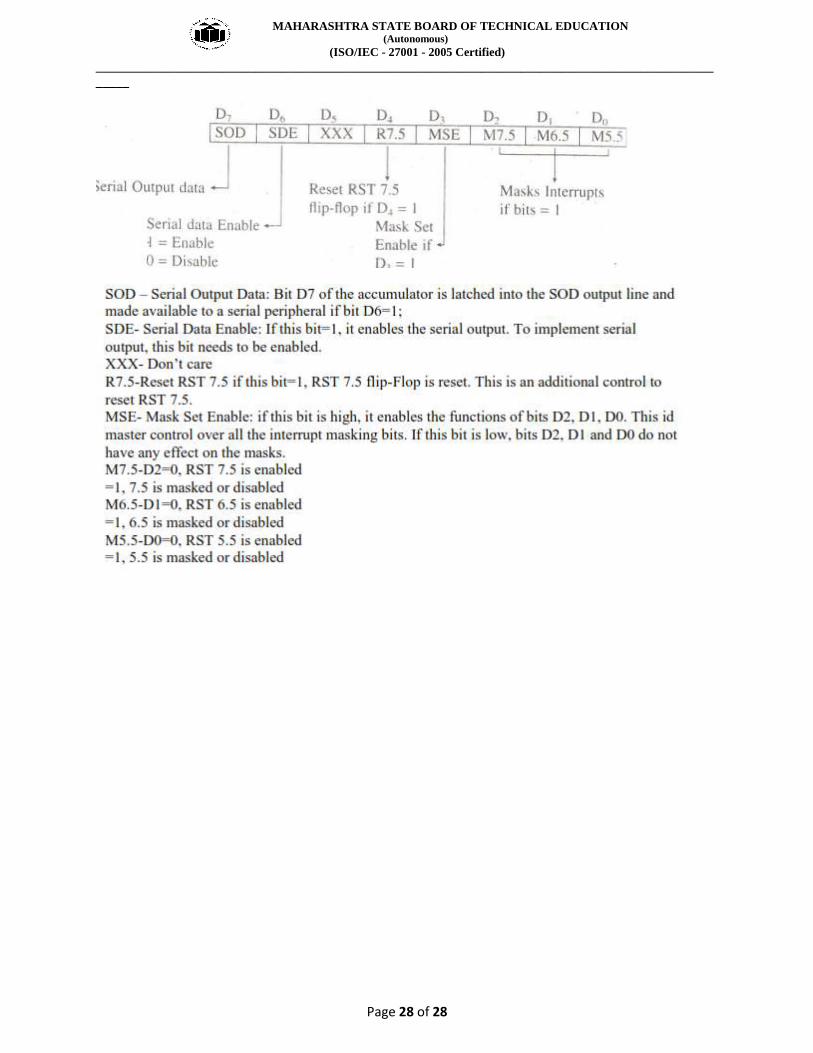
f) Draw SIM instruction format and describe the function of each bit.
Ans:- ( SIM format- 2 mks, description - 2 mks)
MAHARASHTRA STATE BOARD OF TECHNICAL EDUCATION (Autonomous)
(ISO/IEC - 27001 - 2005 Certified)
_____________________________________________________________________________________________
_____
Page 28 of 28