Embed Size (px)
Citation preview
LHCb Collaboration LHCb 2000-114 MuonPublic version7 March 2000
Wire Pad Chambers and Cathode Pad Chambersfor the LHCb Muon System
B. Botchine, V. Lazarev, N. Saguidova, A. VorobyovPetersburg Nuclear Physics Institute (PNPI), Gatchina, Russia
A. Kachtchouk�
, W. Riegler, B. Schmidt, Th. SchneiderEuropean Laboratory for Particle Physics (CERN), CH-1211 Gen`eve 23, Switzerland
�
On leave from PNPI, Gatchina, Russia
M. Gandelman, B. Marechal, D. Moraes, L. de Paula, E. PolycarpoInstituto de F´ısica, Universidade Federal do Rio de Janeiro, Rio de Janeiro, Brazil
Abstract
A proposal for Wire-Pad-Chambers and Cathode-Pad-Chambers for the LHCb MuonSystem is presented. It is shown that a single technology satisfies the requiremetns ofalmost the entire detector, garanteeing maximum uniformity. The muon system layoutbased on this technology is shown, and the chamber geometry specifications together withelectronics considerations are discussed. Am overview of prototype results are presented,followed by considerations on ageing. Finally construction and cost issues are outlined.
1 Introduction
The task for the muon chambers in LHCb is to detect muons within a time window of 25nswith very high efficiency (
�99%) with position resolution in X and Y ranging from 0.5 cm to
30 cm. We expect particle rates of up to 560 kHz/cm� , so in addition the chambers have to copewith high rates and large charge deposits over 10 years of operation.
Wire Pad Chambers (WPCs) and Cathode Pad Chambers (CPCs) are able to satisfy allthese requirements in all the regions of the detector. Table 1 shows the rates and accumulatedcharges for the entire detector.
Except for Region1 and Region2 in M1, the total accumulated charge in 10 years of op-eration is less that 1 C/cm which was proven to be a safe range with respect to aging effects.The only detector limitation of WPCs and CPCs would be gas gain drop due to space chargeeffects in the detector gas which are however negligible up to rates of 1 MHz/cm� .
Two advantages of WPCs and CPCs we consider to be most important:
� The technology can be used in almost the entire detector, guaranteeing maximumuniformity.
� WPCs and CPCs are ordinary Multi Wire Proportional Chambers which are veryrobust and whose performance is very well understood and can be well simulated.
1
Table 1 Rates and accumulated charges in the detector for WPCs and CPCs. The charge is calculatedassuming a gas gain of 1.6� � � .
Station M1 M2 M3 M4 M5
Rate/� � � /interaction � � � � � � � � � � � � � � � � � � � � � � � � � � � � � � � � � � � �
R1 Rate @� � � � � � (kHz/� � � ) 280 10 8 4.8 4.8Rate/� � � + safety (kHz/� � � ) 560 50 400 24 24C/cm/10years @� � � � � � � � 4.2 0.75 0.6 0.36 0.36Rate/channel wire pad (kHz) – 780 730 500 580Rate/channel cathode Pad (kHz)1400 590 550 500 580Rate/� � � /interaction % � � � � � � � � � � � � � � � � � � � � � � � � ' � � � � (
R2 Rate @� � � � � � (kHz/� � � ) 160 4.8 0.8 0.4 0.3Rate + safety (kHz/� � � ) 320 24 4 2 1.6C/cm/10years @� � � � � � � � 2.4 0.36 0.06 0.03 0.024Rate/channel wire pad (kHz) – 750 150 170 150Rate/channel cathode pad (kHz)1600 560 220 130 120Rate/� � � /interaction � � � � � � % � � � � % � � � � ( - � � � � ( - � � � � (
R3 Rate @� � � � � � (kHz/� � � ) 40 1.6 0.16 0.12 0.12Rate/ + safety (kHz/� � � ) 80 8 0.8 0.6 0.6C/cm/10years @� � � � � � � � 0.6 0.12 0.012 0.009 0.009Rate/channel cathode pad 1600 250 30 50 60Rate/� � � /interaction - � � � � � � � � � � ( � � � � � ( � � � � � � � . - � � � � (
R4 Rate @� � � � � � (kHz/� � � ) 10 0.2 0.04 0.03 0.12Rate/ + safety (kHz/� � � ) 20 1 0.2 0.15 0.6C/cm/10years @� � � � � � � � 0.18 0.015 0.003 0.002 0.009Rate/channel wire pad 1600 130 30 115 60
2
2 Muon System Layout
The muon chamber layout is based on the concept of projectivity between the five muon stations.It is fully conform to the so called ”logical layout” described elsewhere [1] and is built with thesmallest possible number of different chamber types, corresponding to the four regions. Inparticular for Regions 1 and 2 it represents an optimal solution from point of view of matchingbetween granularity and number of FE-electronics channels required.
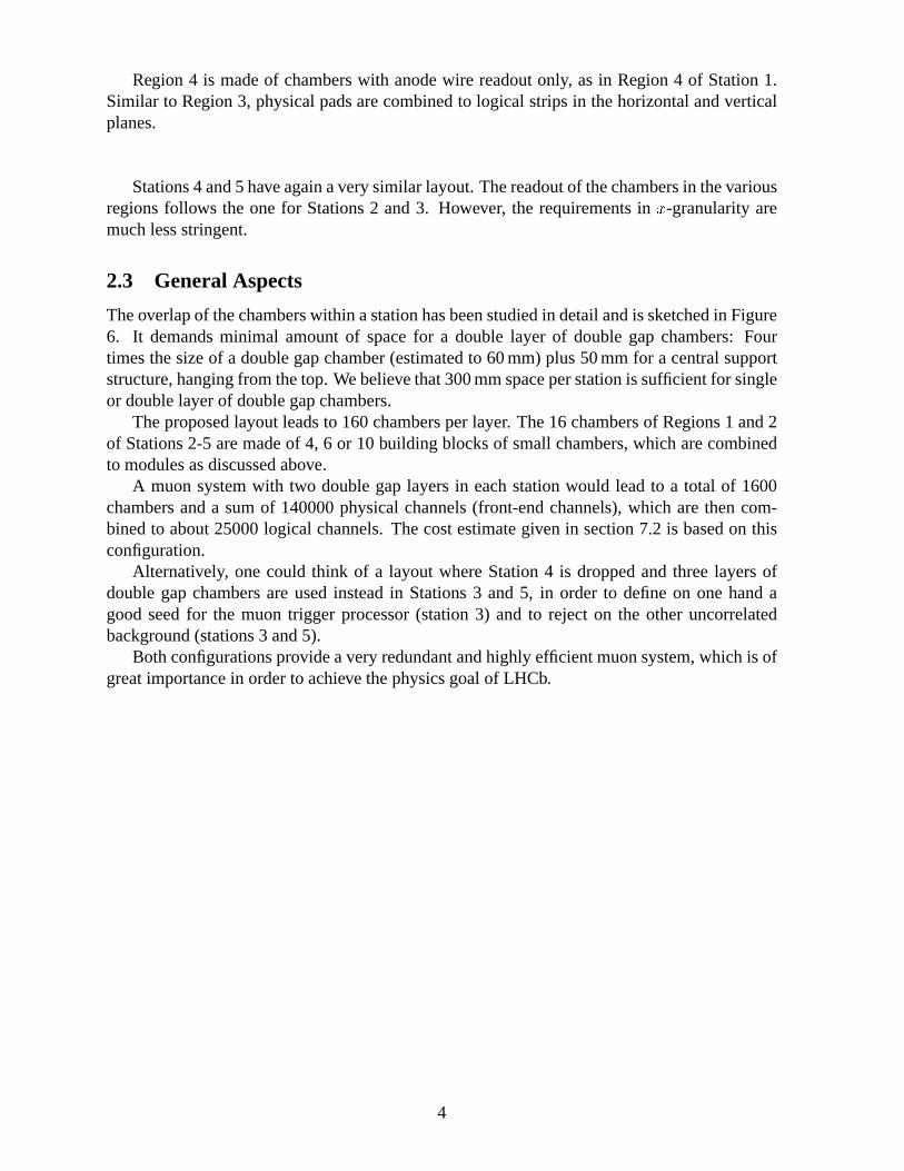
A schematic view of a quadrant of stations 1, 2 and 5 is given in Figures 1-3. They indicateas well the chamber dimensions for the various regions and stations.
2.1 Station M1
Due to the high occupancy in Station M1 the use of logical strips is not possible in any of thefour regions. Furthermore, the logical pads to be used in the trigger have to be split further inregions 2-4 into smaller physical pads in order to stay with the total rate at around 1.5 MHz.
We envisage cathode pad readout in Regions 1 to 3 and anode wire (pad) readout in Region4. The cathode pads in Region 3 are easily accessible from the chamber sides as the chambersare only 20cm wide.
Since Regions 1 and 2 are subject to the highest rates within the muon system and theaccumulated charge is well above 1C/cm over 10 LHC years (Table 1), cathode pad chambersas discussed in this note are not proposed for this area. Micro gap chambers [2] operated withthe same gas mixture might be a possible candidate for this area.
2.2 Stations M2 to M5
Stations 2 and 3 have a similar layout and impose the strongest requirements from granularitypoint of view: 6.25 mm in0 in Region 1. However, since the occupancy is significantly smallerthan in Station M1, logical strips can be used.
The building blocks for Regions 1 and 2 of these stations are small chambers, where therequired0 -granularity is given by anode wire pads and the1 -granularity by cathode pads withinthe same chamber. Four of these building blocks are combined in a module for Region 2, asdepicted in Figure 4. For Region 1 the building blocks have the same height but even less width(cf. Figure 5), in order to allow a modular structure of the whole system with acceptable channeloccupancy. The two double layers in Regions 1 and 2 are put together in such a way that thedistance between the layers along the2 -axis is only 2.5 cm. This reduces the hit multiplicity inthe two layers due to particles traversing the system with some angle to a minimum and helpsto keep the total thickness per station low. Space of about 3.5 cm for the FE-board with theamplifier-shaper-discriminator chips is foreseen on the sides of each building block in theseregions.
Region 3 is made of chambers which have only cathode pad readout, similar to Station 1.Several (physical) pads in the horizontal and vertical plane respectively are grouped togetherto form logical strips. This has the great advantage that no deterioration to the required timeresolution is introduced by signal propagation in strips. Since the surface of a physical channelis anyway limited by the maximum capacitance, the number of additional (physical) channelsis rather small (10-15%).
3
Region 4 is made of chambers with anode wire readout only, as in Region 4 of Station 1.Similar to Region 3, physical pads are combined to logical strips in the horizontal and verticalplanes.
Stations 4 and 5 have again a very similar layout. The readout of the chambers in the variousregions follows the one for Stations 2 and 3. However, the requirements in0 -granularity aremuch less stringent.
2.3 General Aspects
The overlap of the chambers within a station has been studied in detail and is sketched in Figure6. It demands minimal amount of space for a double layer of double gap chambers: Fourtimes the size of a double gap chamber (estimated to 60 mm) plus 50 mm for a central supportstructure, hanging from the top. We believe that 300 mm space per station is sufficient for singleor double layer of double gap chambers.
The proposed layout leads to 160 chambers per layer. The 16 chambers of Regions 1 and 2of Stations 2-5 are made of 4, 6 or 10 building blocks of small chambers, which are combinedto modules as discussed above.
A muon system with two double gap layers in each station would lead to a total of 1600chambers and a sum of 140000 physical channels (front-end channels), which are then com-bined to about 25000 logical channels. The cost estimate given in section 7.2 is based on thisconfiguration.
Alternatively, one could think of a layout where Station 4 is dropped and three layers ofdouble gap chambers are used instead in Stations 3 and 5, in order to define on one hand agood seed for the muon trigger processor (station 3) and to reject on the other uncorrelatedbackground (stations 3 and 5).
Both configurations provide a very redundant and highly efficient muon system, which is ofgreat importance in order to achieve the physics goal of LHCb.
4
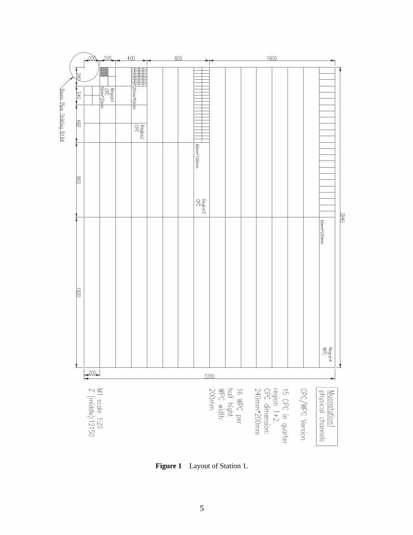
Figure 1 Layout of Station 1.
5
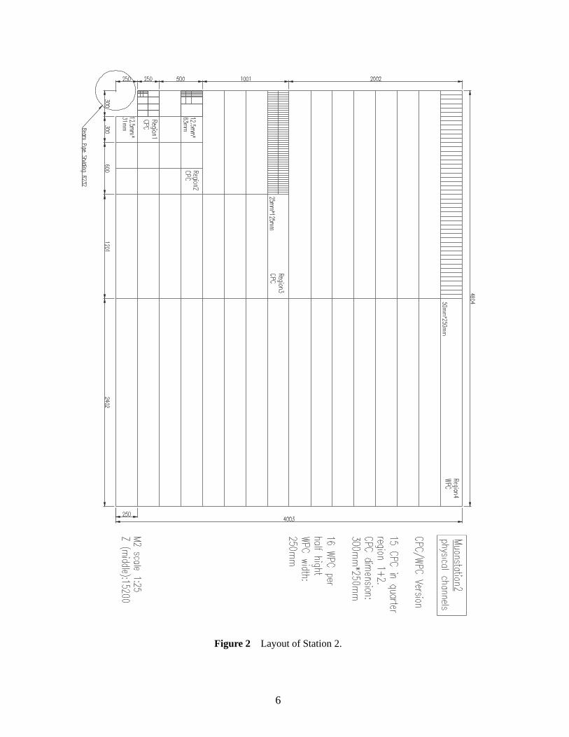
Figure 2 Layout of Station 2.
6
Figure 3 Layout of Station 5.
7
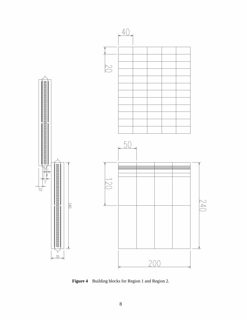
Figure 4 Building blocks for Region 1 and Region 2.
8
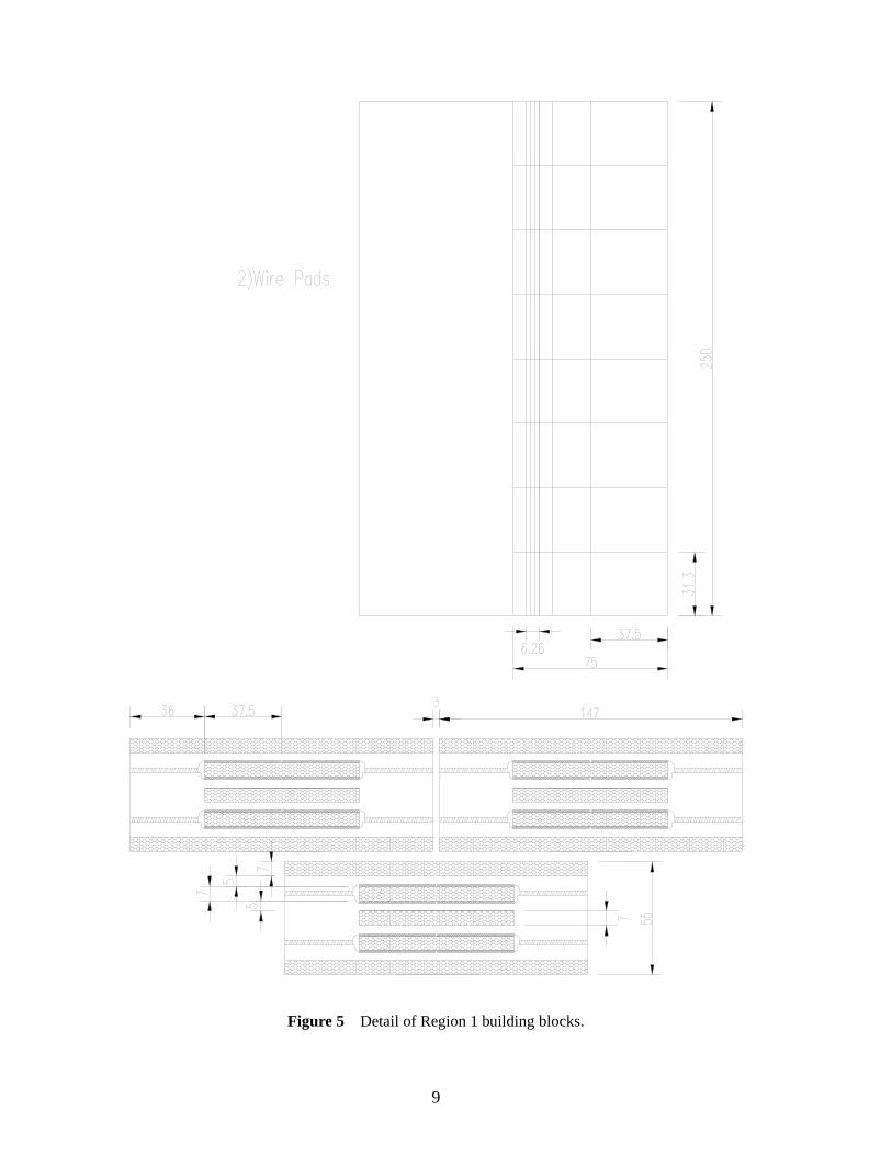
Figure 5 Detail of Region 1 building blocks.
9
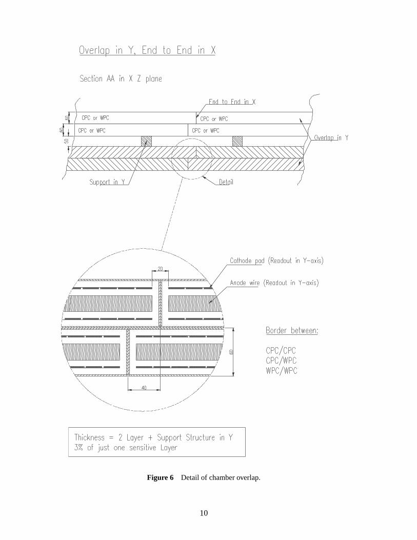
Figure 6 Detail of chamber overlap.
10
15
15
5
5
15
Honeycomb
Fr4(Cu)
cathode V=0
h
hs
cathode V=0
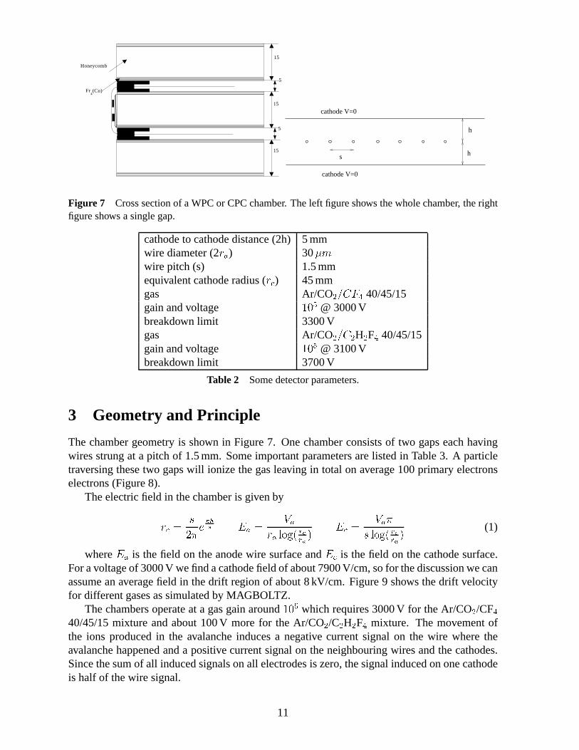
Figure 7 Cross section of a WPC or CPC chamber. The left figure shows the whole chamber, the rightfigure shows a single gap.
cathode to cathode distance (2h)5 mmwire diameter (23 4 ) 30 6 �wire pitch (s) 1.5 mmequivalent cathode radius (3 8 ) 45 mmgas Ar/CO�
9 : ;� 40/45/15
gain and voltage � � @ 3000 Vbreakdown limit 3300 Vgas Ar/CO�
9 :� H� F� 40/45/15
gain and voltage � � @ 3100 Vbreakdown limit 3700 V
Table 2 Some detector parameters.
3 Geometry and Principle
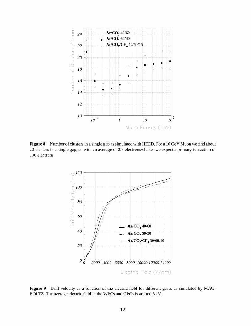
The chamber geometry is shown in Figure 7. One chamber consists of two gaps each havingwires strung at a pitch of 1.5 mm. Some important parameters are listed in Table 3. A particletraversing these two gaps will ionize the gas leaving in total on average 100 primary electronselectrons (Figure 8).
The electric field in the chamber is given by
3 8 < >� ? @B CE F 4 <
H 43 4 I K M O Q RQ T
V F 8 <H 4 ?
> I K M O Q RQ TV (1)
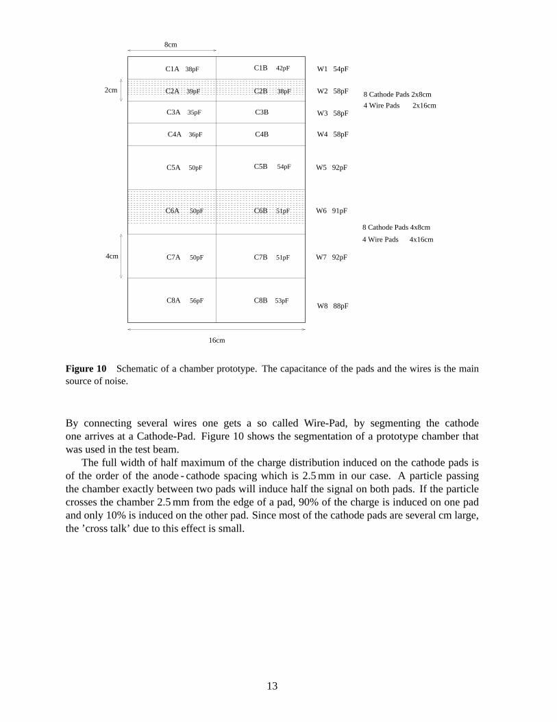
where F 4 is the field on the anode wire surface andF 8 is the field on the cathode surface.For a voltage of 3000 V we find a cathode field of about 7900 V/cm, so for the discussion we canassume an average field in the drift region of about 8 kV/cm. Figure 9 shows the drift velocityfor different gases as simulated by MAGBOLTZ.
The chambers operate at a gas gain around� � which requires 3000 V for the Ar/CO� /CF�40/45/15 mixture and about 100 V more for the Ar/CO� /C� H� F� mixture. The movement ofthe ions produced in the avalanche induces a negative current signal on the wire where theavalanche happened and a positive current signal on the neighbouring wires and the cathodes.Since the sum of all induced signals on all electrodes is zero, the signal induced on one cathodeis half of the wire signal.
11
10
12
14X
16
18X
20Y
22
24
10X -1
1X
10X
10X 2
Z
Ar/CO[
2\ 40/60
Ar/CO[
2\ 60/40
Ar/CO[
2\ /CF
]
4^ 40/50/15
Figure 8 Number of clusters in a single gap as simulated with HEED. For a 10 GeV Muon we find about20 clusters in a single gap, so with an average of 2.5 electrons/cluster we expect a primary ionization of100 electrons.
0_
20Y
40
60`
80a
100X
120X
0_
2000 4000 6000`
8000a
10000 12000 14000
Ar/CO[
2\ 40/60
Ar/CO[
2\ 50/50
Ar/CO[
2\ /CF
]
4^ 30/60/10
Figure 9 Drift velocity as a function of the electric field for different gases as simulated by MAG-BOLTZ. The average electric field in the WPCs and CPCs is around 8 kV.
12
8cm
16cm
C3A
4 Wire Pads 4x16cm
C4A
C1A C1B
C8A C8B
C7A C7B
C5A C5B
C3B
C4B
C6BC6A
C2BC2A2cm
4cm
38pF
39pF
35pF
36pF
50pF
50pF
50pF
56pF
42pF
38pF
54pF
51pF
51pF
53pFW8 88pF
W7 92pF
W6 91pF
W5 92pF
W4 58pF
W3 58pF
W2 58pF
W1 54pF
8 Cathode Pads 2x8cm
4 Wire Pads 2x16cm
8 Cathode Pads 4x8cm
Figure 10 Schematic of a chamber prototype. The capacitance of the pads and the wires is the mainsource of noise.
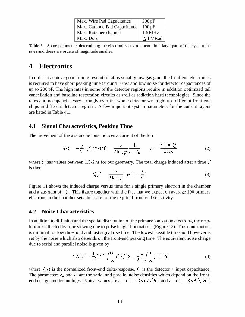
By connecting several wires one gets a so called Wire-Pad, by segmenting the cathodeone arrives at a Cathode-Pad. Figure 10 shows the segmentation of a prototype chamber thatwas used in the test beam.
The full width of half maximum of the charge distribution induced on the cathode pads isof the order of the anode - cathode spacing which is 2.5 mm in our case. A particle passingthe chamber exactly between two pads will induce half the signal on both pads. If the particlecrosses the chamber 2.5 mm from the edge of a pad, 90% of the charge is induced on one padand only 10% is induced on the other pad. Since most of the cathode pads are several cm large,the ’cross talk’ due to this effect is small.
13
Max. Wire Pad Capacitance 200 pFMax. Cathode Pad Capacitance100 pFMax. Rate per channel 1.6 MHzMax. Dose b � MRad
Table 3 Some parameters determining the electronics environment. In a large part of the system therates and doses are orders of magnitude smaller.
4 Electronics
In order to achieve good timing resolution at reasonably low gas gain, the front-end electronicsis required to have short peaking time (around 10 ns) and low noise for detector capacitances ofup to 200 pF. The high rates in some of the detector regions require in addition optimized tailcancellation and baseline restoration circuits as well as radiation hard technologies. Since therates and occupancies vary strongly over the whole detector we might use different front-endchips in different detector regions. A few important system parameters for the current layoutare listed in Table 4.1.
4.1 Signal Characteristics, Peaking Time
The movement of the avalanche ions induces a current of the form
d O e V < f hH j O e V F O 3 O e V V < h� I K M Q RQ T�
e o e q e q < 3 �4 I K M Q RQ T� H 4 6 (2)
wheree q has values between 1.5-2 ns for our geometry. The total charge induced after a timesis then t
O e V < h� I K M Q RQ TI K M O � o e
e qV
(3)
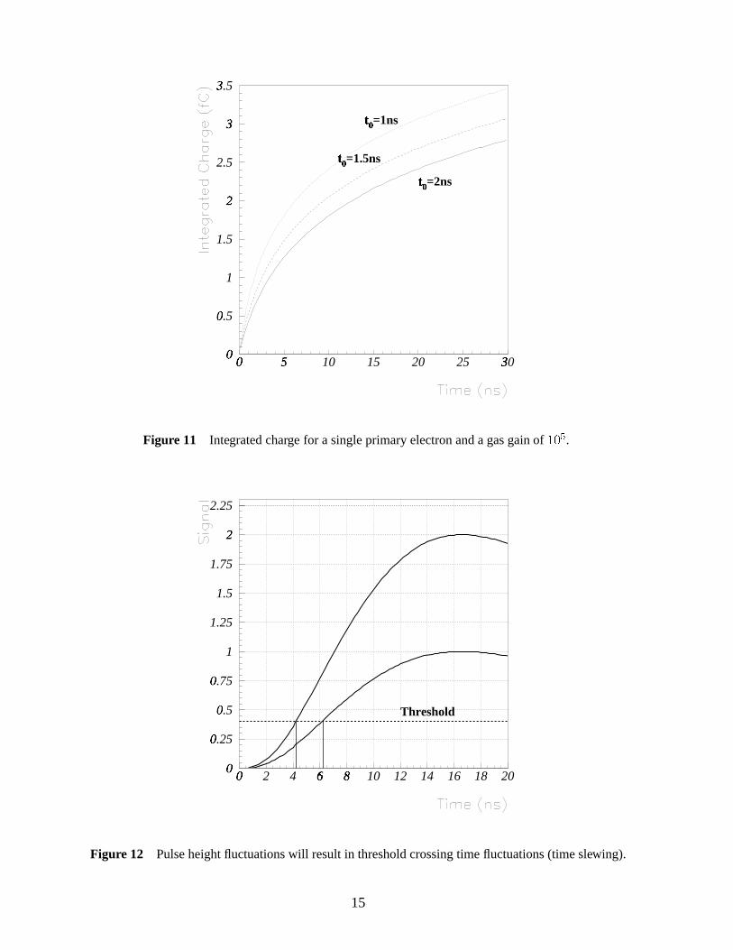
Figure 11 shows the induced charge versus time for a single primary electron in the chamberand a gas gain of� � . This figure together with the fact that we expect on average 100 primaryelectrons in the chamber sets the scale for the required front-end sensitivity.
4.2 Noise Characteristics
In addition to diffusion and the spatial distribution of the primary ionization electrons, the reso-lution is affected by time slewing due to pulse height fluctuations (Figure 12). This contributionis minimal for low threshold and fast signal rise time. The lowest possible threshold however isset by the noise which also depends on the front-end peaking time. The equivalent noise chargedue to serial and parallel noise is given by
F u : � < �� @ � v : � w� w
x y O e V � { e o �� d � v w� w
x O e V � { e (4)
wherex O e V
is the normalized front-end delta-response,:
is the detector + input capacitance.The parameters@ v and
d v are the serial and parallel noise densities which depend on the front-end design and technology. Typical values are@ v } � f � � H 9 � � 2 and
d v } � f - � � 9 � � 2 .
14
0�
0.5�
1
1.5
2�
2.5
3�
3.5�
0�
5�
10 15 20 25 30�
t�
0� =2ns
t�0
� =1.5ns
t�
0� =1ns
Figure 11 Integrated charge for a single primary electron and a gas gain of� � .
0�
0.25�
0.5�
0.75�
1
1.25
1.5
1.75
2�
2.25
0�
2 4 6�
8�
10 12 14 16 18 20
Threshold
Figure 12 Pulse height fluctuations will result in threshold crossing time fluctuations (time slewing).
15
Approximating the signal leading edge by a straight line and setting the threshold to the lowestpossible value (5� of the noise) we find the time slewing contribution to be
� � �e � @ v : � e � � ��� �� � � o �� �� � I K M O � o � �� � V (5)
where a and b are dimensionless constants characterizing the shape of the delta response and Gis the gas gain. We see that the time slewing effect is proportional to the detector capacitanceand inversely proportional to the gas gain. The function has a minimum ate � b - � ¡ � e q , so theoptimum peaking time for the WPCs and CPCs isb ' � > . Since very high bandwidth amplifiersare not desired in a large system we want a peaking time around� � � > .
4.3 Front-end input resistance and capacitance
The capacitance determining the serial noise is the detector capacitance plus input capacitance.Therefore the input capacitance should be as low as possible. The detector capacitance
: £ � �together with the front-end input resistance¤ � v define a time constant¥ � v < ¤ � v : £ � � whichacts as an integration stage. Therefore the chamber signal effectively ’sees’ a circuit whichconsists of an integrator together with the preamp circuit, i.e.¤ � v and
: £ � � decrease the systempeaking time. In order to limit this peaking time dependence on the detector capacitance theinput resistance should be as small as possible.
4.4 Tail cancellation
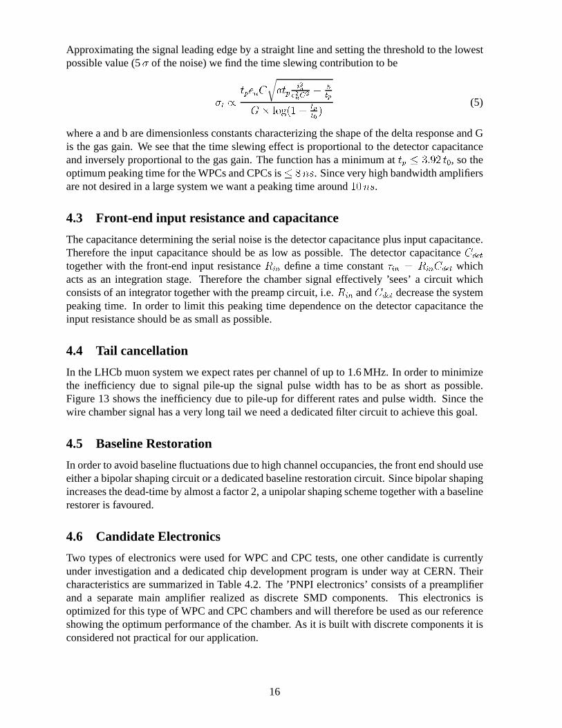
In the LHCb muon system we expect rates per channel of up to 1.6 MHz. In order to minimizethe inefficiency due to signal pile-up the signal pulse width has to be as short as possible.Figure 13 shows the inefficiency due to pile-up for different rates and pulse width. Since thewire chamber signal has a very long tail we need a dedicated filter circuit to achieve this goal.
4.5 Baseline Restoration
In order to avoid baseline fluctuations due to high channel occupancies, the front end should useeither a bipolar shaping circuit or a dedicated baseline restoration circuit. Since bipolar shapingincreases the dead-time by almost a factor 2, a unipolar shaping scheme together with a baselinerestorer is favoured.
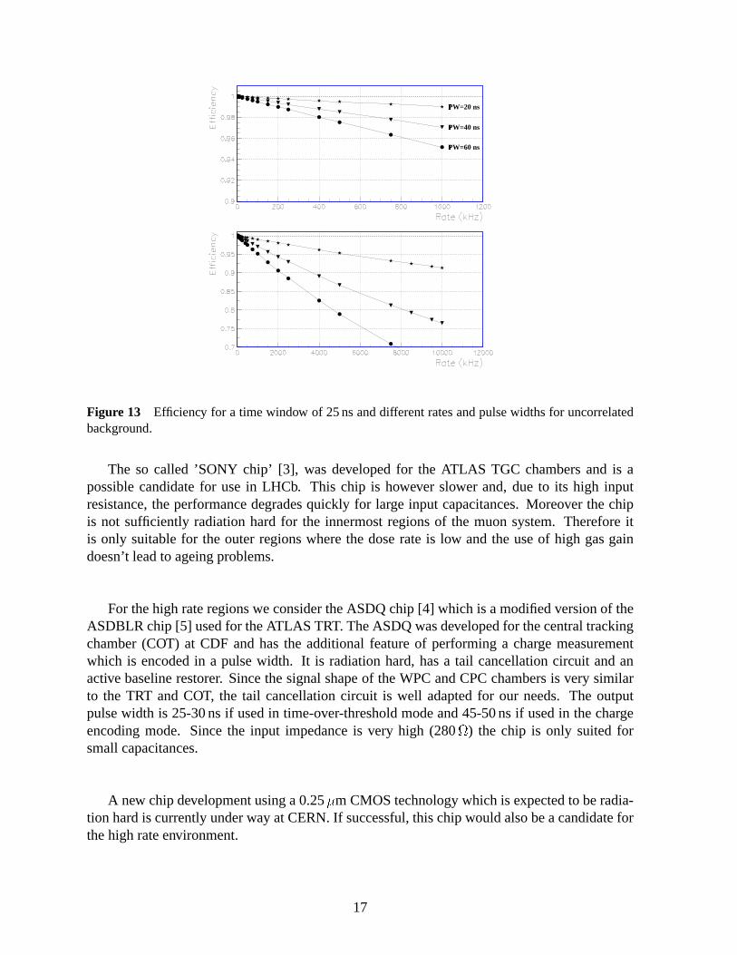
4.6 Candidate Electronics
Two types of electronics were used for WPC and CPC tests, one other candidate is currentlyunder investigation and a dedicated chip development program is under way at CERN. Theircharacteristics are summarized in Table 4.2. The ’PNPI electronics’ consists of a preamplifierand a separate main amplifier realized as discrete SMD components. This electronics isoptimized for this type of WPC and CPC chambers and will therefore be used as our referenceshowing the optimum performance of the chamber. As it is built with discrete components it isconsidered not practical for our application.
16
PW=20 ns§
PW=40 ns§
PW=60 ns§
Figure 13 Efficiency for a time window of 25 ns and different rates and pulse widths for uncorrelatedbackground.
The so called ’SONY chip’ [3], was developed for the ATLAS TGC chambers and is apossible candidate for use in LHCb. This chip is however slower and, due to its high inputresistance, the performance degrades quickly for large input capacitances. Moreover the chipis not sufficiently radiation hard for the innermost regions of the muon system. Therefore itis only suitable for the outer regions where the dose rate is low and the use of high gas gaindoesn’t lead to ageing problems.
For the high rate regions we consider the ASDQ chip [4] which is a modified version of theASDBLR chip [5] used for the ATLAS TRT. The ASDQ was developed for the central trackingchamber (COT) at CDF and has the additional feature of performing a charge measurementwhich is encoded in a pulse width. It is radiation hard, has a tail cancellation circuit and anactive baseline restorer. Since the signal shape of the WPC and CPC chambers is very similarto the TRT and COT, the tail cancellation circuit is well adapted for our needs. The outputpulse width is 25-30 ns if used in time-over-threshold mode and 45-50 ns if used in the chargeencoding mode. Since the input impedance is very high (280¨ ) the chip is only suited forsmall capacitances.
A new chip development using a 0.256 m CMOS technology which is expected to be radia-tion hard is currently under way at CERN. If successful, this chip would also be a candidate forthe high rate environment.
17
model PNPI SONY ASDQ
technology discrete comp. SONY Bipolar MAXIM Bipolarinput resistance 25 ¨ 80 ¨ 260 ¨peaking time @ C
£ � � =0 4 ns 11 ns 8 nspeaking time @ C
£ � � =100 pF 7 ns 20 nsENC @ 10 pF 1800 e- 1500 e- 2300 e-sensitivity @ C
£ � � =0 10 mV/fC 5.6 mV/fC 25 mV/fCsensitivity @ C
£ � � =100 pF 6 mV/fC 3.5 mV/fCRadiation Limit
�50 kRad
�5 MRad
Av. Pulsewidth @ 100 pF 60 ns 90 ns 25 nsBaseline restoration no yes yesMax. rate tested 1 MHz 15 MHzChannels/Chip 4 8Power Consumption/channel 59 mW 40 mWCost per Channel 1.7 SFr 4 SFr
Table 4 Some electronics parameters.
18
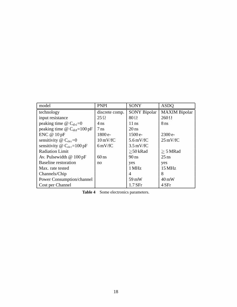
Table 5 Percentage of events with hits in the neighbouring pads within 20 ns
Electronics Gas Mixture Gas Gain Anode Pads Cathode Pads
a) PNPI Ar/CO� /CF� 2 � 10 4 % 3 %b) SONY Ar/CO� /CF� 2 � 10 5% 4%c) SONY Ar/CO�
9 :� H� F� 4 � 10 20 % 13 %
5 Performance
Several WPC and CPC prototypes were tested in the T7 and T11 beams at CERN. A CPCprototype with various pad sizes (from� � � cm to ' � � « cm) was constructed and tested inautumn 1998, using the readout design presented in the Technical Proposal [7] and was shownto be reliable.
A first WPC prototype with wire pad readout only was tested in May 1999. Further WPCprototypes have been tested in November 1999. They contained cathode strips as well ascathode pads. Here we present results from the prototype shown in Figure 10, with wire pads
% � � « cm� large and cathode pads% � ' cm� large.
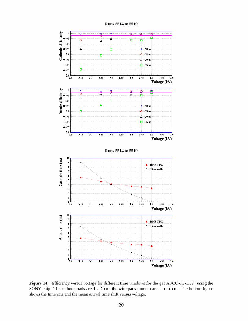
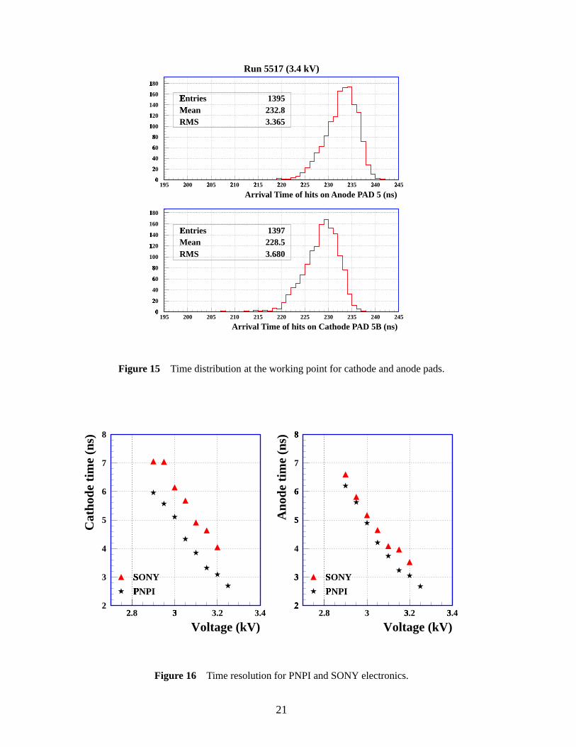
Figure 14 shows the efficiency as a function of the high voltage for the gas Ar/CO� /C� H� F�40/45/15 using the SONY chip. Cuts were applied in the charge and number of hits in thescintillators in order to select single particle events. For a time window of 25 ns the chamber isfully efficient at a voltage of 3.25 kV corresponding to a gas gain of� � � � . To get to 99 %efficiency in 20 ns, it is necessary to operate at higher gain, namely at 3.4 kV. The chamber wasoperated up to 3.7 kV before breakdown occured. Hence, in the outer detector regions, wherethe rates and therefore the total charge deposits are low, one has still a large operating plateauof 300 V which is very convenient. Figure 15 shows an example of the time distribution at theworking point. The time resolution (RMS) is about 3.0-4 ns for the anodes and 3-4.5 ns for thecathodes in the operating range of 3.25 -3.5 kV. The measured shift of the mean arrival time isabout 1.5-2 ns / 100V.
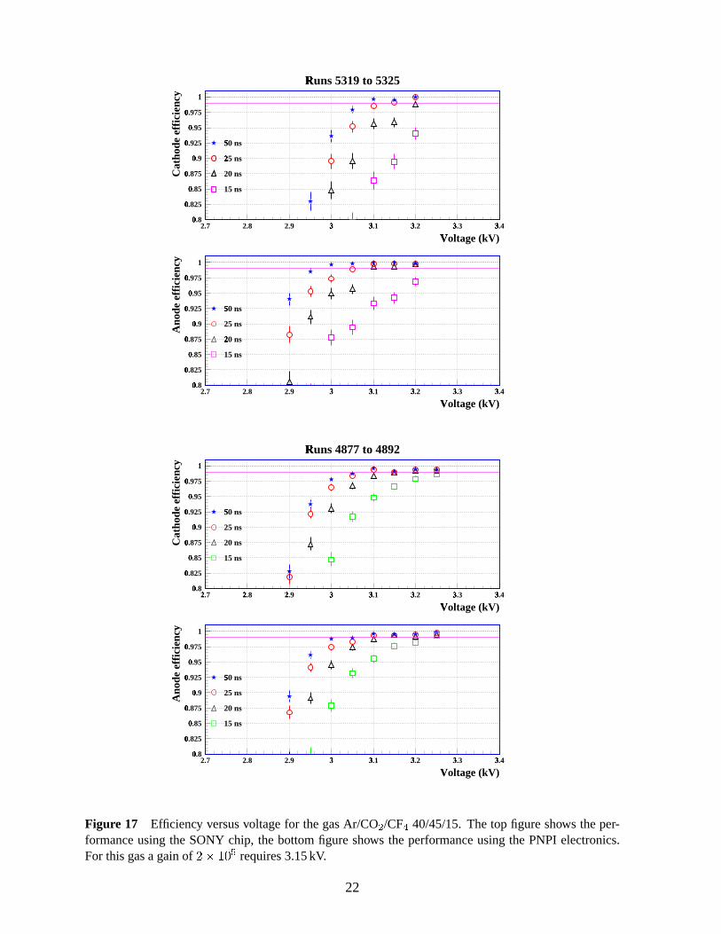
As discussed in the last section, the peaking time and the sensitivity of the SONY chip de-creases rapidly for increased input capacitance. Therefore, in addition to the chamber geometry,the time resolution is largely influenced by the electronics. Using optimized electronics one canimprove the performance to arrive at high efficiency even for lower gas gain. Figure 17 showsa comparison between the efficiencies obtained with SONY chip and PNPI electronics for thestandard gas mixture Ar/CO� /CF� (40/45/15). Figure 16 compares the time resolution for thePNPI and SONY electronics.
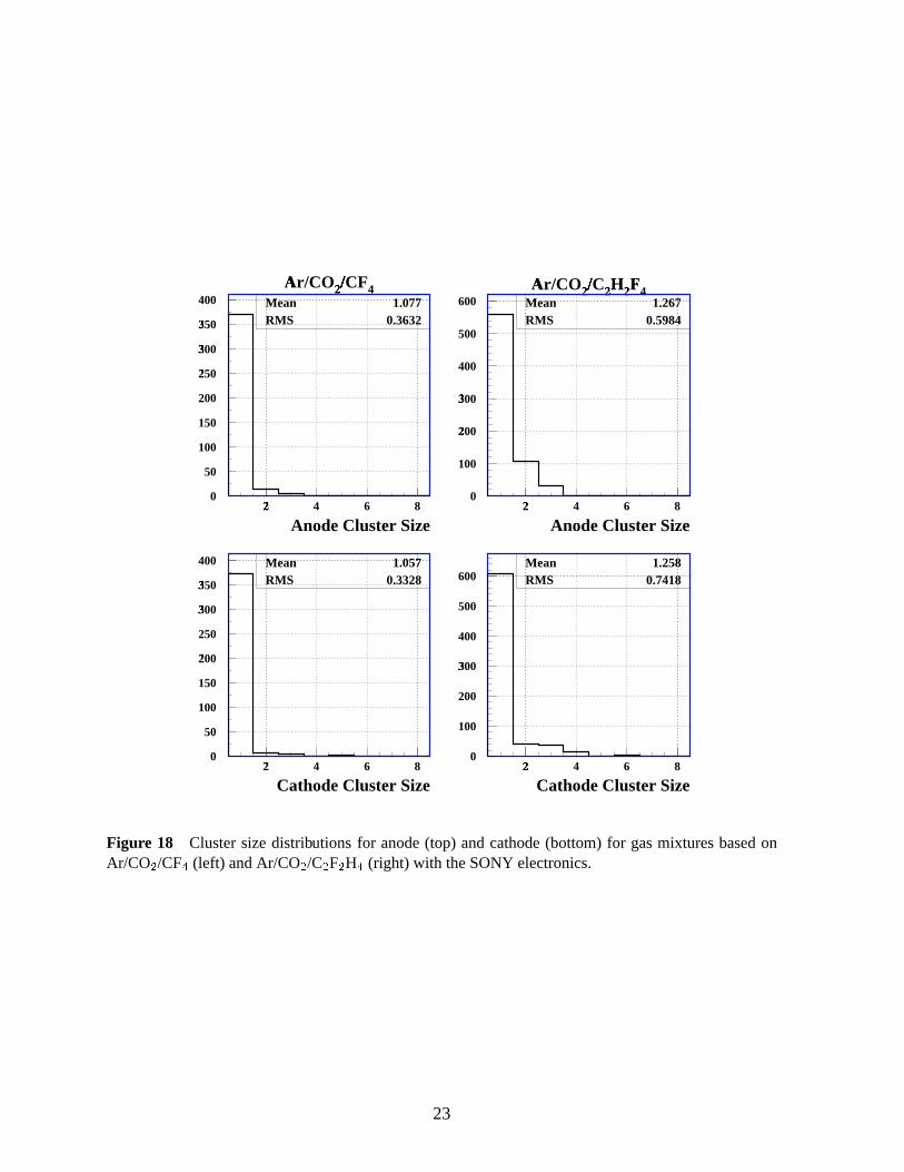
To study crosstalk events were selected using the best possible choice of hodoscope chan-nels, in order to have the particles crossing the center of the pad and still have enough statistics.Table 5 presents the percentage of events which have more than one hit within the 20 ns timewindow. Since the gas Ar/CO� /C� H� F� allows operation of the chamber at higher gas gain,which is necessary for thew SONY chip, the increase of crosstalk at the corresponding voltageis explained. Optimizations can be done to decrease the capacitive coupling between the pads,reducing then the crosstalk and cluster size.
In order to analyse the dependence of the efficiency on rate, including pile-up effects, eventswere selected with at least one hit in the scintillators facing the pad and no cut on the chargewas applied. Events with hits on the hodoscope strips facing neighboring pads were rejected, in
19
Runs 5514 to 5519
0.8®
0.825®
0.85®
0.875®
0.9®
0.925®
0.95®
0.975®
1¯
3.1°
3.15°
3.2°
3.25°
3.3°
3.35°
3.4°
3.45°
3.5°
3.55°
3.6°
20 ns
Voltage (kV)±
Cat
hode
eff
icie
ncy
25 ns²50 ns
³
15 ns
0.8®
0.825®
0.85®
0.875®
0.9®
0.925®
0.95®
0.975®
1
3.1°
3.15°
3.2°
3.25°
3.3°
3.35°
3.4°
3.45°
3.5°
3.55°
3.6°
20 ns²25 ns
50 ns³
Voltage (kV)±
Ano
de e
ffic
ienc
y
15 ns
Runs 5514 to 5519
0®12
´3°45
µ6¶78
·9¸10
¯
3.1°
3.15°
3.2°
3.25°
3.3°
3.35°
3.4°
3.45°
3.5°
3.55°
3.6°
RMS TDC¹Time walk
Voltage (kV)±
Cat
hode
tim
e (n
s)
0®12
3°4º5µ6¶78
·9¸10
3.1°
3.15°
3.2°
3.25°
3.3°
3.35°
3.4°
3.45°
3.5°
3.55°
3.6°
RMS TDC
Time walk
Voltage (kV)±
Ano
de t
ime
(ns)
Figure 14 Efficiency versus voltage for different time windows for the gas Ar/CO� /C� H� F� using theSONY chip. The cathode pads are» � ¼ cm, the wire pads (anode) are» � � ¾ cm. The bottom figureshows the time rms and the mean arrival time shift versus voltage.
20
0¿
2À
0
40
6Á
0
8Â
0
100
1Ã
20
1Ã
40
160
1Ã
80
195 200 205 210 215 220 225 230 235 240 245
Run 5517 (3.4 kV)
EÄ
ntriesMÅ
eanRMS
1395 232.8 3.365
Arrival Time of hits on Anode PAD 5 (ns)
EÄ
ntriesMeanRMS
1397 228.5 3.680
Arrival Time of hits on Cathode PAD 5B (ns)
0¿
2À
0
4Æ
0
6Á
0
8Â
0
1Ã
00
1Ã
20
140
1Ã
60
1Ã
80
1Ã
95 2À
00 2À
05 2À
10 2À
15 2À
20 2À
25 2À
30 2À
35 2À
40 2À
45
Figure 15 Time distribution at the working point for cathode and anode pads.
2
3
4
5
6
7
8
2.8Ç
3È
3.2 3.4
SONYÉ
PNPIÊ
Voltage (kV)
Cat
hode
tim
e (n
s)
SONYÉ
PNPIÊ
Voltage (kV)
Ano
de t
ime
(ns)
2Ç
3È
4
5Ë
6Ì
7
8Í
2.8 3 3.2È
3.4È
Figure 16 Time resolution for PNPI and SONY electronics.
21
Runs 5319 to 5325Î
0.8®
0.825®
0.85®
0.875®
0.9®
0.925®
0.95®
0.975®
1¯
2.7 2.8 2.9 3°
3.1°
3.2°
3.3°
3.4°
20 ns
Voltage (kV)±
Cat
hode
eff
icie
ncy
25 ns²50 ns
³
15 ns
0.8®
0.825®
0.85®
0.875®
0.9®
0.925®
0.95®
0.975®
1
2.7 2.8 2.9 3°
3.1°
3.2°
3.3°
3.4°
20 ns²25 ns
50 ns³
Voltage (kV)±
Ano
de e
ffic
ienc
y
15 ns
Runs 4877 to 4892Î
0.8®
0.825®
0.85®
0.875®
0.9®
0.925®
0.95®
0.975®
1¯
2.7´
2.8´
2.9´
3°
3.1°
3.2°
3.3°
3.4°
20 ns
Voltage (kV)±
Cat
hode
eff
icie
ncy
25 ns
50 ns³
15 ns
0.8®
0.825®
0.85®
0.875®
0.9®
0.925®
0.95®
0.975®
1
2.7 2.8 2.9 3°
3.1°
3.2°
3.3°
3.4°
20 ns
25 ns
50 ns³
Voltage (kV)±
Ano
de e
ffic
ienc
y
15 ns
Figure 17 Efficiency versus voltage for the gas Ar/CO� /CF� 40/45/15. The top figure shows the per-formance using the SONY chip, the bottom figure shows the performance using the PNPI electronics.For this gas a gain ofÏ � � � requires 3.15 kV.
22
MeanRMS
1.077 0.3632
Anode Cluster Size
AÑ
r/CO2Ò /
ÓCF4
MeanRMS
1.267 0.5984
Anode Cluster Size
AÑ
r/CO2Ò /
ÓC2
Ò HÔ
2Ò F
Õ4
MeanRMS
1.057 0.3328
Cathode Cluster Size
MeanRMS
1.258 0.7418
Cathode Cluster Size
0
50
100
150
200
2Ò
50
3Ö
00
3Ö
50
400
2Ò
4 6 80
100
2Ò
00
3Ö
00
400
500
600
2Ò
4 6 8
0
50
100
150
2Ò
00
250
3Ö
00
3Ö
50
400
2Ò
4 6 80
100
200
3Ö
00
400
500
600
2Ò
4 6 8
Figure 18 Cluster size distributions for anode (top) and cathode (bottom) for gas mixtures based onAr/CO� /CF� (left) and Ar/CO� /C� F� H� (right) with the SONY electronics.
23
P×
ad rate (KHz)
Ano
de e
ffic
ienc
y
20 ns25 ns50 ns
15 ns0
Ø.9
0Ø
.92
0Ø
.94
0Ø
.96
0Ø
.98
1
0Ø
100 2Ù
00 3Ú
00 4Û
00 5Ü
00 6Ý
00 7Þ
00
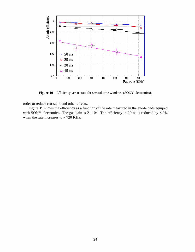
Figure 19 Efficiency versus rate for several time windows (SONY electronics).
order to reduce crosstalk and other effects.Figure 19 shows the efficiency as a function of the rate measured in the anode pads equiped
with SONY electronics. The gas gain is 2� 10 . The efficiency in 20 ns is reduced byß 2%when the rate increases toß 720 KHz.
24
6 Ageing
Detailed ageing studies of the wire chambers have been performed at PNPI in the frameworkof the CMS End Cap Muon System programme (CMS Note 1999/011). One should stress thatthe WPC/CPC chambers are made precisely from the same materials as the CMS chambers anduse the same gas mixture. Therefore, the results obtained for the CMS chambers are directlyapplicable to the proposed WPC/CPC chambers. These tests showed that with the gas mixturesAr/CO
�/CF
�in the relative proportions 30/50/20 as well as 40/50/10 the deterioration of the
chamber performance (gas gain and dark currents) was not observed up to the accumulatedcharges of 13 Coul/cm wire. Note however that the irradiation of the chambers was local witha Sr-90 beta source.
The global irradiation tests of the CMS chambers have been started last year at GIF facilityat CERN. So far only a modest accumulated charge has been collected ( 0.2 Coul/cm wire).These tests will be continued in March/April 2000. We are planning to perform the local ageingtests at PNPI with the Ar/CO
�/C
�H
�F
�gas mixtures using a WPC prototype. These tests will
be started in Feb 2000. Also global ageing tests of the WPC filled with the Ar/CO�/C
�H
�F
�gas
mixture are planned to be performed at GIF in March/April 2000 in parallel with the CMS tests.
25
7 Realization
7.1 Construction
The WPC/CPC chambers are specially designed to make their construction as simple aspossible. The wires are wound along the short side of the chamber that make it possible to usethe small wire spacing (1.5 mm) needed for good time resolution without additional supportstructure. The WPC chambers use simple cathode planes without any pad/strip structure. Thereis no severe requirement to the flatness of the cathode plane to be produced in industry.
The FE-electronics is arranged in a very simple way on the chamber body. The con-struction of such chambers can be easily organised in any physics laboratory. The WPCchambers will be used in Region 4 of the LHCb Muon System covering about 75% of the totalarea. The CPC chambers designed for Region 3 have a very simple cathode pad structure : 2rows of % � � � cm� pads with readout from both sides of the chamber. The construction of thesechambers is not much different from the WPC construction. A similar type of construction willbe used in Region 2 and 1 of M2 - M5.
PNPI has many years experience in wire chamber construction. At present the instituteis involved in the construction of the Cathode Strip Chambers for the CMS End Cap MuonSystem [8] which has close similarity with the LHCb chambers. PNPI can organise a specialproduction line of the WPC/CPC chambers and would be able to assemble an essential part ofthese chambers. The production scheme assumes that there will be at least one more productionline in some other laboratory and that the major parts for the chambers will be produced bycollaborating groups with involvement of industry.
7.2 Costing
Table 7.2 shows the cost estimates for the muon system. To estimate the manpower we consid-ered one chamber per week per person. The contribtutions to the total cost which are technologyspecific are mainly the chambers, FE-chip and boards and HV and gas systems. they amountto slightly less than 2450 kCHF. Some of the estimates for parts of the electronics chain needfurther substantiation. As the total budget for the muon system is about 6000 k, the final sumleaves about 500 k available for manpower.
26
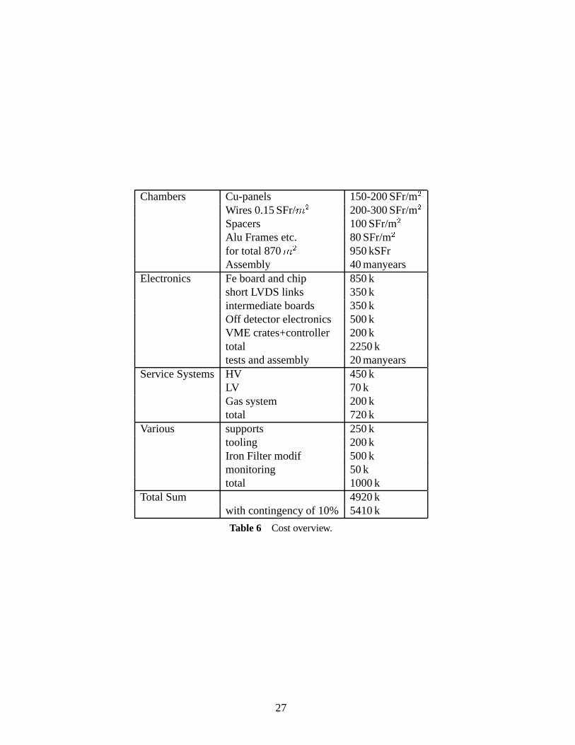
Chambers Cu-panels 150-200 SFr/m�
Wires 0.15 SFr/� � 200-300 SFr/m�
Spacers 100 SFr/m�
Alu Frames etc. 80 SFr/m�
for total 870� � 950 kSFrAssembly 40 manyears
Electronics Fe board and chip 850 kshort LVDS links 350 kintermediate boards 350 kOff detector electronics 500 kVME crates+controller 200 ktotal 2250 ktests and assembly 20 manyears
Service Systems HV 450 kLV 70 kGas system 200 ktotal 720 k
Various supports 250 ktooling 200 kIron Filter modif 500 kmonitoring 50 ktotal 1000 k
Total Sum 4920 kwith contingency of 10% 5410 k
Table 6 Cost overview.
27
8 Conclusions� WPCs and CPCs have shown to satisfy the requirements for almost the entire LHCb muon
system.
� Except for Region 1 and Region 2 in M1, the accumulated charge in 10 years of operationis less that 1 C/cm.
� For Regions 3 and 4 in stations M3 to M5 the rates are low enough to allow a gas gain ofup to 5� � � , hence using the SONY chip will provide satisfactory operation.
� For M1 and the inner regions of M2-M5 the high rates require gas gain less than� � � � , sofor safe operation a front end electronics chip must be found that matches the performanceof the PNPI chip and also can stand a dose of up to 1 MRad.
� Detectors similar to CPC’s but with different gain and geometry are under developmentfor the hot spots in M1.
28
References
[1] P.Colrain et.al, LHCb 2000-016 Muon
[2] S. Getz et. a, Micro-Gap Chambers for the Inner Region of the LHCb Muon System,LHCb 2000-004 Muon
[3] O. Sasaki et. al., Amplifier-Shaper-Discriminator ICs, ATLAS internal muon note, Oct.1999
[4] W. Bokhari et al., The ASDQ ASIC, CDF internal note, April 1998.
[5] ATLAS inner detector TDR. CERN/LHCC/97-17, M. Newcomer et al., ASDBLR chipoperational studies at CERN, ATLAS internal note 29.1. 1996.
[6] B. Bochine et.al, Wire Pad chambers for the LHCb muon system. LHCb 2000-003 Muon
[7] LHCb Technical Proposal, CERN/LHCC 98-4, LHCC/P4, 20 February 1998
[8] CMS MUON TDR, CERN/LHCC 97-32, CMS TDR 3, 15 December 1997
29