Embed Size (px)
Citation preview
Wireless Power Transmission With Brook's Coil Adaptation and
Class E Power Amplifier
by
Lum Jian Kai
Dissertation submitted in partial fulfilment of
the requirements for the
Bachelor of Engineering (Hons)
(Electrical & Electronics Engineering)
MAY 2014
Universiti Teknologi Petronas
Bandar Seri Iskandar
31750 Tronoh
Perak Darul Ridzuan
Copyright 2014
by
Lum Jian Kai, 2014
i
CERTIFICATION OF APPROVAL
WIRELESS POWER TRANSMISSION WITH BROOK'S COIL ADAPTATION
AND CLASS E POWER AMPLIFIER
by
Lum Jian Kai
A project dissertation submitted to the
Electrical & Electronics Engineering Programme
Universiti Teknologi PETRONAS
in partial fulfilment of the requirement for the
Bachelor of Engineering (Hons)
(Electrical & Electronics Engineering)
Approved:
__________________________
IR. Dr. Perumal Nallagownden
Project Supervisor
UNIVERSITI TEKNOLOGI PETRONAS
TRONOH, PERAK
MAY 2014

ii
CERTIFICATION OF ORIGINALITY
This is to certify that I am responsible for the work submitted in this project, that the
original work is my own except as specified in the references and
acknowledgements, and that the original work contained herein have not been
undertaken or done by unspecified sources or persons.
__________________________ LUM JIAN KAI

iii
ABSTRACT
Wireless Power Transmission (WPT) via Magnetic Resonance Coupling will be the
future method in transmitting electrical power. The vision of transferring power
wirelessly will provide a solution to power equipments in unreachable areas.
Success of WPT depends on distance of power transmission which requires great
improvement. This project propose a multilayer Brook's coil design and class E
power amplifier to increase transmission distance. The use of zero voltage
switching MOSFET operation in a 375kHz class E power amplifier, serves to reduce
power loss and increase current supplied to transmitter coil. A DC voltage of 13.34V
was obtained at 30cm with 3.068mW power output at receiver end. This resulted to
15 times increased in transmission distance from previous project. Maximum output
power achievable for this project was 418mW at 10cm transmission distance.

iv
AWARDS & RECOGNITIONS
Electrex People's Choice Award & Best Creative Idea Award
𝟑𝟑𝐫𝐝 SEDEX Final Year Project GOLD Medal
in 33rd
𝟑𝟑𝐫𝐝 SEDEX Most Creative Idea Award

v

vi

vii
ACKNOWLEDGEMENTS
I would like to express my deepest gratitude and appreciation to IR. DR. Perumal
Nallagownden for his guidance and support throughout this project. His advice in
progressing this project have been a valuable knowledge and experience for me to
take into my future undertakings.
My gratitude extends to all lecturers in Electrical and Electronics Engineering
Department that have equipped me with all the knowledge and skills, both technical
and my personal development through this 4 years of degree course. The patience
and openness in advising me is greatly appreciated.
I would also like to thank all lab technicians for their full support in the completion
of this project and friendliness that made this project more meaningful.
Finally, the utmost important appreciation goes to my family for their impeccable
support and encouragement throughout my life.
viii
TABLE OF CONTENTS
CERTIFICATION OF APPROVAL ........................................................................................ i
CERTIFICATION OF ORIGINALITY ...................................................................................ii
ABSTRACT ............................................................................................................................. iii
AWARDS & RECOGNITIONS .............................................................................................. iv
ACKNOWLEDGEMENTS .................................................................................................... vii
LIST OF FIGURES .................................................................................................................. x
LIST OF TABLES ................................................................................................................... xi
CHAPTER 1 ............................................................................................................................ 1
INTRODUCTION ............................................................................................................... 1
1.1 Background of Study ................................................................................................. 1
1.2 Problem Statement ..................................................................................................... 2
1.3 Objectives .................................................................................................................. 2
1.4 Scope of Study ........................................................................................................... 3
CHAPTER 2 ............................................................................................................................ 4
LITERATURE REVIEW .................................................................................................... 4
2.1 Magnetic Resonance Coupling .................................................................................. 4
2.2 Coil Design ................................................................................................................ 5
2.3 Power Electronics Circuit - Power Amplifier ............................................................ 6
CHAPTER 3 ............................................................................................................................ 8
METHODOLOGY .............................................................................................................. 8
3.1 Research Methodology .............................................................................................. 8
3.2 Design Characteristics of Magnetic Resonance Coupling Circuit ............................. 8
3.3 Class E Power Amplifier .......................................................................................... 10
3.4 Oscillator .................................................................................................................. 13
3.6 Project Activities ...................................................................................................... 16
CHAPTER 4 .......................................................................................................................... 19

ix
RESULTS AND DISCUSSION ........................................................................................ 19
4.1 Overview .................................................................................................................. 19
4.2 Class E Power Amplifier .......................................................................................... 19
4.3 Brook's Coil Design Adaptation .............................................................................. 24
4.4 Wireless Power Transmission Prototype ................................................................. 26
4.5 Wireless Power Transmission Prototype Operational Guide ................................... 30
CHAPTER 5 .......................................................................................................................... 32
CONCLUSION AND RECOMMENDATION ................................................................. 32
REFERENCES ...................................................................................................................... 34

x
LIST OF FIGURES
Figure 1 : Wireless Power Transmission System Summary ..................................................... 9
Figure 2 : Class E Power Amplifier Circuit .............................................................................. 11
Figure 3 : 555 Timer Structure and 50% duty cycle circuit .................................................... 13
Figure 4 : Coil Cross Section ................................................................................................... 14
Figure 5 : FYP 1 Gantt Chart ................................................................................................... 17
Figure 6 : FYP 2 Gantt Chart ................................................................................................... 18
Figure 7 : Multisim Simulation Circuit .................................................................................... 20
Figure 8 : Voltage across MOSFET & and 50% Square Waveform ......................................... 21
Figure 9 : ZVS Operation ........................................................................................................ 21
Figure 10 : Simulated waveform across inductor resembling coil ......................................... 22
Figure 11 : 250kHz (left) & 264kHz (right) Inductor Voltage Waveform ............................... 23
Figure 12 : ZVS Waveform at 370kHz ..................................................................................... 24
Figure 13 : Measuring Coil Inductance with FLUKE PM6303A ............................................... 25
Figure 14 : Wireless Power Transmission Demonstration ..................................................... 27
Figure 15 : Low Power Dissipation with Zero Voltage Switching ........................................... 27
Figure 17 : Graph of Power (mW) against Distance (cm) ...................................................... 28
Figure 16 : Sinusoidal High Voltage Supplied to Transmitter Coil ......................................... 28
Figure 18 : Voltage(V) and Current(mA) Against Distance (cm) ............................................ 29
Figure 19 : Wireless Power Transmission Prototype ............................................................. 30

xi
LIST OF TABLES
Table 1 : MOSFET Selection ................................................................................................... 12
Table 2 : 555 Timer Operation ............................................................................................... 14
Table 3 : Calculated & Practical Specification ........................................................................ 23
Table 4 : Coil Specification ..................................................................................................... 25
Table 5: Measured Coil Specification Result .......................................................................... 25
Table 6 : Comparison with Previous Project .......................................................................... 29
Table 7 : Prototype Technical Specification ........................................................................... 31
1
CHAPTER 1
INTRODUCTION
1.1 Background of Study
Wireless power transmission(WPT) dates back to 1899 where Nikola Tesla designed
the Wardenclyffe Tower with the sole purpose to use resonance effect in
transmission of electricity [1],[2],[3],[4]. From that stand point, many research was
developed and conducted to successfully transmit power wirelessly. The
consideration on using antenna technology for this purpose have seen many
challenges despite the long distance power transfer capability. Challenges include
effects of earths atmospheric conditions and the technology's side effect on living
organisms [1].
With that, the wireless technology strives for success in using magnetic resonance
coupling in which is acknowledged to be the most efficient technique in WPT that
are not affected by the antenna's setback, capable within the middle range
transmission distance [1]. In 2007, Massachusetts Institute of Technology(MIT)
have demonstrated successfully, the usage of magnetic resonance coupling by
lighting a 60W bulb from a distance of 2 meters apart between transmitter and
receiver coils and have since moved on in setting up Witricity, a company that
develops WPT products for the commercial market. The application since then have
been many which include charging electric vehicle and smart phones wirelessly to
name a few [1],[3],[4],[5],[6]. However, the distance remain in the mid range level
and position between the transmitter and receiver are required to be rigidly aligned
for energy transfer.
2
There are many other research conducted since MIT's breakthrough, mostly targeted
at increasing power transfer efficiency by addressing the use of power amplifiers [5],
studying the frequency in which magnetic resonance operates most efficiently and
the duty cycle or wave pattern in the transmitter coils have any effect on magnetic
field strength generation [3],[7]. These information are useful to design an optimum
level of WPT technology and this is important to address the magnetic field issue
which require further insight into power losses by these circuits [6].
1.2 Problem Statement
The WPT has a wide range of application in terms of powering all electrical and
electronics machines or equipments. The elimination of cables and wires used to
supply electrical energy will save cost in production and installation. In developing
countries, rural areas are experiencing limited access to electricity as an ongoing
issue due to unviable financial setting up of conventional electricity grid [8]. With
that, this technology will bring possibilities in supplying electrical power to
unreachable areas where installing electric cables are expensive due to the
environmental boundary. The requirement to transmit at longer distance with
magnetic resonance coupling technology requires improvement to sustain reliable
and feasible applications.
1.3 Objectives
To improve Magnetic Resonance Coupling Wireless Power Transmission distance by
1. implementing and matching low power dissipation class E power amplifier
circuit with wireless power transmission that will overcome restriction in
supplying higher power to transmitter coil.
2. implementing multilayer coil design with Brook's coil concept adaptation to
cater for higher power supplied from power amplifier circuit without causing
coil overheating or alteration to wireless power transmission configuration.

3
1.4 Scope of Study
This project study will cover :
design and build power electronics circuit with low power dissipation for
high current conduction.
design and build multilayer coil to cater for higher power input supplied by
power amplifier.
the use of magnetic resonance coupling technology to transmit electric power
wirelessly

4
CHAPTER 2
LITERATURE REVIEW
2.1 Magnetic Resonance Coupling
The technology behind magnetic resonance coupling lies in magnetic field
propagation between a transmitter and a receiver at the same frequency called
resonant frequency. The principal is focused on resonating the energy back and forth
in a specified area of effect in which enables a strongly coupled magnetic field,
transferring energy at the highest efficiency. The rest follows Faraday's Law and
Lenz's Law for electromagnetic induction [2], [3],[7].
Based on [9], the frequency of resonance will affect the Q-factor of the resonator that
is also influenced by inductance and resistance of coil. With higher Q-Factor, the
power transfer efficiency will increase due to higher coupling effect [9]. Following
that, the inductance and capacitor used to obtain resonance effect will produce LC
cancellation that causes the resistance across the L and C to be low at resonant
frequency and this increases Q-factor [6]. According to [6] and [9], the power
efficiency is affected by design parameters of transmitter and receiver coil focusing
on increasing Q-Factor and resonant frequency configuration.
Apart from resonant frequency selection and coil design, the waveform highlighted
by [2], [3] ,[5] and [7] for magnetic field induction in accordance to Faraday's Law is
a sine wave. In fact, researched done by [7] have discovered that sine wave provided
highest efficiency compared to other waveforms. The sine wave input to the
transmitter coil in radiating magnetic field was accomplished by using an oscillator
with adjustable duty cycle to convert DC source into alternating current of significant
power and frequency [2], [5]. According to [3], the wireless power transmission
efficiency was inversely proportional to the duty cycle after the maximum duty cycle
5
have been achieved. Furthermore, [2] have mentioned a 15% estimated efficiency of
implemented oscillator in which [5] have resorted to using power amplifier to
increase efficiency.
Despite the success of generating magnetic field, performance of WPT system as a
whole is questioned by [6] with consideration on coil performance but also regarding
power efficiency of power electronics circuit that generated the sine wave. [6]
emphasized the need to consider power losses before the coil on the basis that a
decrease in output power of circuit components will be limiting power flowing to the
coil. Furthermore, based on magnetic field effect, the magnetic field strength is
directly proportional to current [10] and with high power losses in circuit
components, the coil will be hindered from maximum magnetic field generation in
which justifies concerns of [6] in the importance of considering power electronics
efficiency.
2.2 Coil Design
In designing a high efficiency coil, [6] and [9] have emphasized the requirement to
have high Q-Factor by increasing inductance and reducing resistance value. The
multilayer coil proposed by [11], [12], and [13] consists of stacked layers of coils on
top of each other where the cross sectional area increases with each stack. Following
that, the internal resistance decreases as the stack of coil increases [12]. Moreover,
the inductance will increase while diameter of coil remain unchanged, contributing to
high efficiency small coil design in which is suitable for WPT operation [14].
Despite the high efficiency and low internal resistance of multilayer coil, the design
requires consideration in terms of skin effect, proximity effect and displacement
current [13], [14]. Although a higher frequency increases Q-Factor [6], [9], the
increase in frequency of operation will increase AC resistance due to skin effect and
proximity effect that in fact decreases Q-Factor [13], [14]. Furthermore, [14] have
discovered the increase in AC resistance is most distinct when the stacked layers are
increased beyond the maximum amount.
Based on the fact that there is a maximum stacked layer in which varies for different
coil dimensions, [11] and [15] demonstrates brook's coil design that is a multilayer
6
coil orientation with a square cross sectional area and controlled dimensions by ratio,
standardized the amount of stacked layer for maximum performance. This type of
design enables optimum inductance value at a finite length of wire [11].
In spite of brook's coil and multilayer coil design, the use of magnetic core for WPT
coil design was not effective because of core saturation [11] and negative effect to
surrounding wireless devices [13]. With that, [11] and [13] have justified using air
core in which is efficient and does not affect inductance with an increase in current.
Therefore, consideration is required in terms of frequency of operation with number
of stack layers and the application of core in coil design is crucial.
2.3 Power Electronics Circuit - Power Amplifier
Power amplifiers are categorised into linear power amplifiers such as class A, B and
AB and switching amplifiers with class C, D, E and F. In the case of WPT
application, the switching amplifier produces substantial improvement towards
power efficiency especially related to class E power amplifier design. The design
process is tedious although simple to construct with success in WPT implementation
[16], [17].
Basically, the class E power amplifier uses lesser components compared to other
classes in the same category and achieve higher efficiency [16]. According to [17],
the calculation in design consists of long iterative methods in which is a setback to
simple circuit construction. In order to fully comprehend the advantages of class E
power amplifiers, a simple analytical design method was implemented by [17] to
produce a high approximation design. However, the full and complete mathematical
model is covered by [16].
With the design process made simple, there have been success in implementing this
power amplifier in WPT system. [18] and [19] have significantly improved WPT
system efficiency to above 80% by using class E power amplifier. The improvement
of system efficiency was due to reduced power dissipation in power amplifier
through zero voltage switching [16] that increased power transfer to coils [18], [19].

7
Therefore, concerns in power efficiency of circuit components by [6] was addressed
by class E power amplifier application in WPT. However, the application on WPT
using magnetic resonance coupling at low frequency range have not been explored
and due to frequency effect on coil resistance, the research on this will be useful in
developing high efficiency WPT system at low frequency range.
8
CHAPTER 3
METHODOLOGY
3.1 Research Methodology
This project will be divided into coil design and efficiency of power electronics
circuit for higher power conduction to transmitter coil with the aim and thus longer
distance of transmission to receiver coil that will consists of 3 sections :
1. Class E Power Amplifier
2. Oscillator
3. Brook's Coil design
The research methodology will address concept and design of class E power
amplifier with driving circuit consisting of an oscillator. Following enhancement of
power efficiency in transmitter coil, design adaptation of brook's coil concept will be
developed to increase coil efficiency that will enhance power transfer capability
through stronger magnetic field strength. Apart from that, magnetic field strength
will be explained with reference to current through the coil to improve transmission
distance.
3.2 Design Characteristics of Magnetic Resonance Coupling Circuit
A WPT system mainly consists of power source, oscillator, power amplifier,
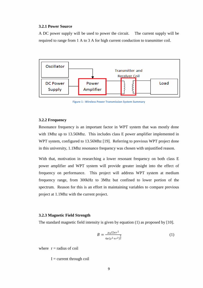
transmitter and receiver coil as summarized in Figure 1. In this section, the design
criterias are highlighted before detailed project concepts are explained.
9
3.2.1 Power Source
A DC power supply will be used to power the circuit. The current supply will be
required to range from 1 A to 3 A for high current conduction to transmitter coil.
Figure 1 : Wireless Power Transmission System Summary
3.2.2 Frequency
Resonance frequency is an important factor in WPT system that was mostly done
with 1Mhz up to 13.56Mhz. This includes class E power amplifier implemented in
WPT system, configured to 13.56Mhz [19]. Referring to previous WPT project done
in this university, 1.1Mhz resonance frequency was chosen with unjustified reason.
With that, motivation in researching a lower resonant frequency on both class E
power amplifier and WPT system will provide greater insight into the effect of
frequency on performance. This project will address WPT system at medium
frequency range, from 300kHz to 3Mhz but confined to lower portion of the
spectrum. Reason for this is an effort in maintaining variables to compare previous
project at 1.1Mhz with the current project.
3.2.3 Magnetic Field Strength
The standard magnetic field intensity is given by equation (1) as proposed by [10].
𝐵 =𝜇0𝐼2𝜋𝑟2
4𝜋 𝑧2+𝑟2 32
(1)
where r = radius of coil
I = current through coil
10
From this equation, a higher current will generate higher magnetic field intensity and
larger area of magnetic coverage. Therefore, this project promotes high current
conduction to transmitter coil which is made possible with class E power amplifier
explained in the next section.
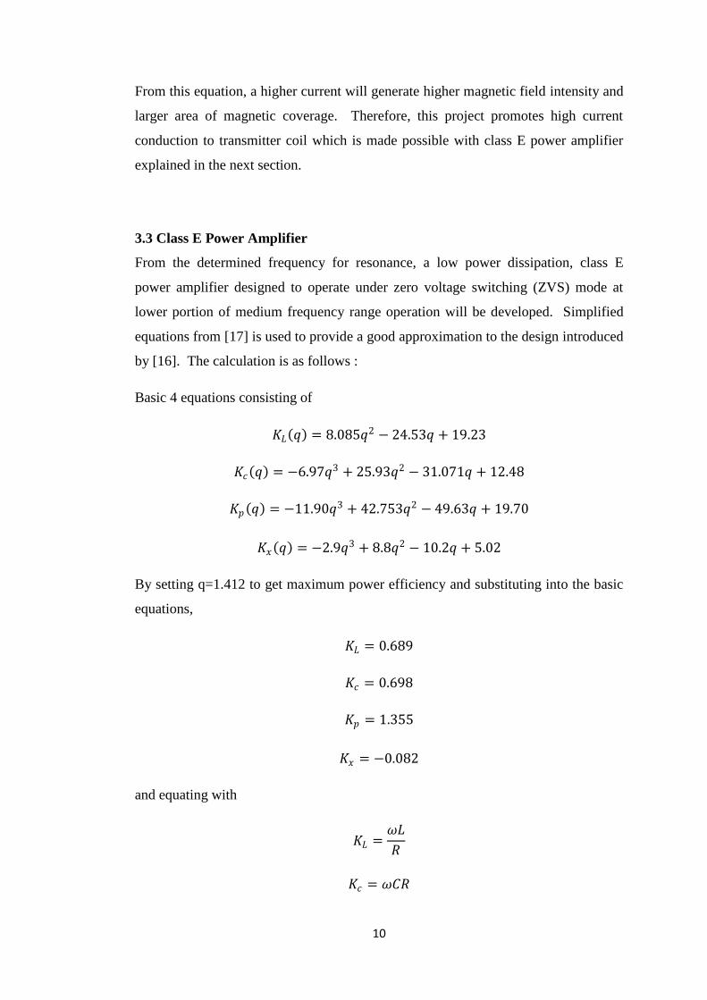
3.3 Class E Power Amplifier
From the determined frequency for resonance, a low power dissipation, class E
power amplifier designed to operate under zero voltage switching (ZVS) mode at
lower portion of medium frequency range operation will be developed. Simplified
equations from [17] is used to provide a good approximation to the design introduced
by [16]. The calculation is as follows :
Basic 4 equations consisting of
𝐾𝐿 𝑞 = 8.085𝑞2 − 24.53𝑞 + 19.23
𝐾𝑐 𝑞 = −6.97𝑞3 + 25.93𝑞2 − 31.071𝑞 + 12.48
𝐾𝑝 𝑞 = −11.90𝑞3 + 42.753𝑞2 − 49.63𝑞 + 19.70
𝐾𝑥 𝑞 = −2.9𝑞3 + 8.8𝑞2 − 10.2𝑞 + 5.02
By setting q=1.412 to get maximum power efficiency and substituting into the basic
equations,
𝐾𝐿 = 0.689
𝐾𝑐 = 0.698
𝐾𝑝 = 1.355
𝐾𝑥 = −0.082
and equating with
𝐾𝐿 =𝜔𝐿
𝑅
𝐾𝑐 = 𝜔𝐶𝑅
11
𝐾𝑝 =𝑃𝑜𝑢𝑡𝑅
𝑉𝐷𝐷2
𝐾𝑥 =𝑋
𝑅
the components value required for ZVS operation will be determined at resonance
frequency as the operating frequency. These calculations will provide inductance
and capacitance value responsible for MOSFET switching on and off at zero voltage,
thus contributing towards low power dissipation.
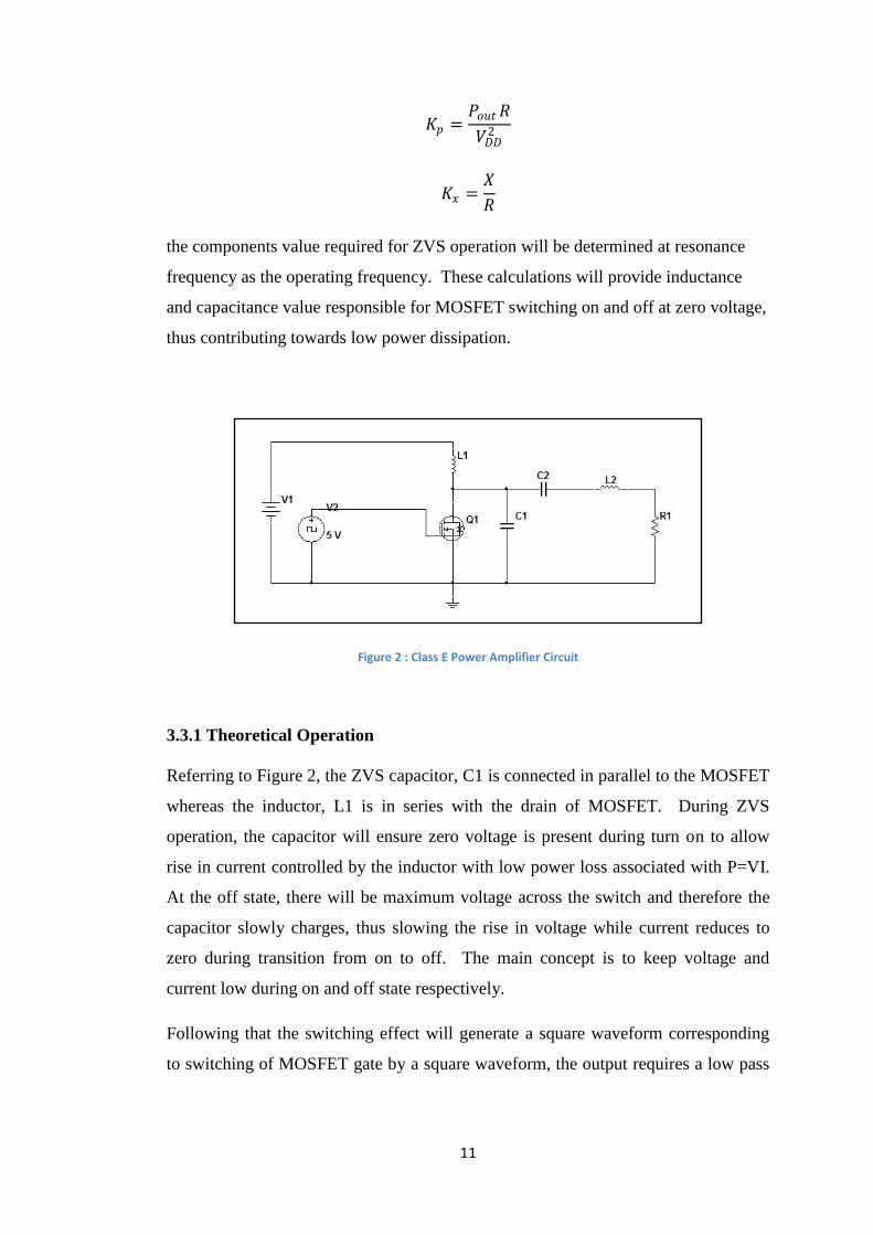
Figure 2 : Class E Power Amplifier Circuit
3.3.1 Theoretical Operation
Referring to Figure 2, the ZVS capacitor, C1 is connected in parallel to the MOSFET
whereas the inductor, L1 is in series with the drain of MOSFET. During ZVS
operation, the capacitor will ensure zero voltage is present during turn on to allow
rise in current controlled by the inductor with low power loss associated with P=VI.
At the off state, there will be maximum voltage across the switch and therefore the
capacitor slowly charges, thus slowing the rise in voltage while current reduces to
zero during transition from on to off. The main concept is to keep voltage and
current low during on and off state respectively.
Following that the switching effect will generate a square waveform corresponding
to switching of MOSFET gate by a square waveform, the output requires a low pass
12
filter to generate a pure sine waveform. Using LC filter with resonance effect, the
value of L2 and C2 are calculated using :
𝑓 =1
2𝜋 𝐿𝐶 (2)
At desired resonance frequency, the Brook's coil will be used to replace the
inductance and operate at resonance with capacitor connected in series. The value of
capacitor is calculated using equation (2) at resonant frequency. With a lower power
dissipation in the power electronics circuit, a higher current can be supplied to the
coil without overheating the power MOSFET, provided that the MOSFET model is
chosen with low 𝑅𝐷𝑆(𝑂𝑁). Total design parameters and calculated values are
discussed in results section.
3.3.2 MOSFET Selection
In a class E power amplifier, the MOSFET influences ZVS performance due to
parasitic capacitance and internal resistance. Therefore, a power MOSFET have the
characteristic of low parasitic capacitance and internal resistance with high output
power in which will operate within requirements. 2 different types of power
MOSFET are evaluated and listed in Table 1.
Table 1 : MOSFET Selection
Model IRF530 IRF540
Manufacturer International Rectifier International Rectifier
𝑉𝑑𝑠 , 𝐼𝑑 100 V , 14 A 100 V , 44 A
𝐶𝑑𝑠 200 pF 210 pF
𝑅𝑑𝑠 0.160 0.044
From the evaluation, IRF530 MOSFET will provide a better ZVS performance due
to lower 𝐶𝑑𝑠 and lower power dissipation for a class E power amplifier operation
despite higher 𝑅𝑑𝑠 [18]. Furthermore, a higher current will certainly improve
magnetic field of transmitter coil and a detailed explanation was covered in magnetic
field strength section.
13
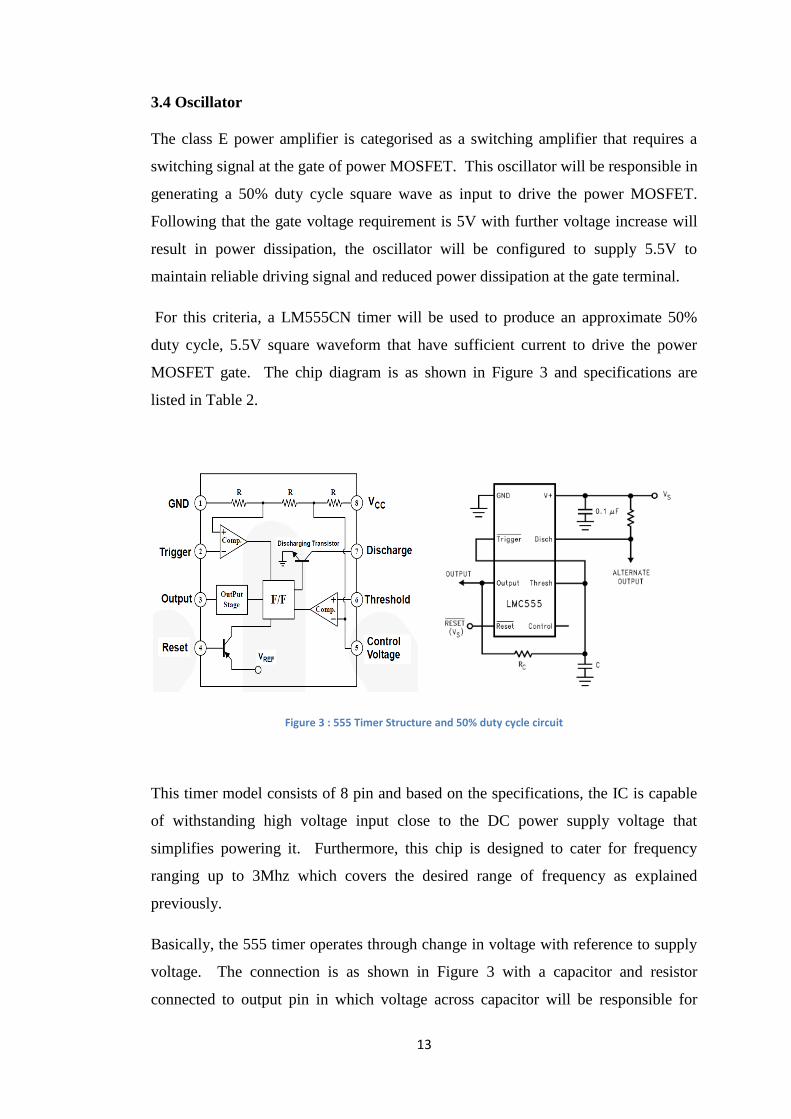
3.4 Oscillator
The class E power amplifier is categorised as a switching amplifier that requires a
switching signal at the gate of power MOSFET. This oscillator will be responsible in
generating a 50% duty cycle square wave as input to drive the power MOSFET.
Following that the gate voltage requirement is 5V with further voltage increase will
result in power dissipation, the oscillator will be configured to supply 5.5V to
maintain reliable driving signal and reduced power dissipation at the gate terminal.
For this criteria, a LM555CN timer will be used to produce an approximate 50%
duty cycle, 5.5V square waveform that have sufficient current to drive the power
MOSFET gate. The chip diagram is as shown in Figure 3 and specifications are
listed in Table 2.
Figure 3 : 555 Timer Structure and 50% duty cycle circuit
This timer model consists of 8 pin and based on the specifications, the IC is capable
of withstanding high voltage input close to the DC power supply voltage that
simplifies powering it. Furthermore, this chip is designed to cater for frequency
ranging up to 3Mhz which covers the desired range of frequency as explained
previously.
Basically, the 555 timer operates through change in voltage with reference to supply
voltage. The connection is as shown in Figure 3 with a capacitor and resistor
connected to output pin in which voltage across capacitor will be responsible for
14
changing the voltage level of trigger pin (pin 2) and threshold pin (pin 6). The
operation is explained in Table 2.
Table 2 : 555 Timer Operation
Pin Voltage Level Output State CR Relation
Trigger (2) 1
3𝑉𝑐𝑐
High Output charges capacitor through
resistor to 2
3𝑉𝑐𝑐
Threshold (6) 2
3𝑉𝑐𝑐
Low Capacitor discharges through
resistor to 1
3𝑉𝑐𝑐
The process repeats to form a square waveform with frequency controlled by
capacitor and resistor value, calculated using equation (3).
𝑓 =1
1.4𝑅𝐶𝐶 (3)
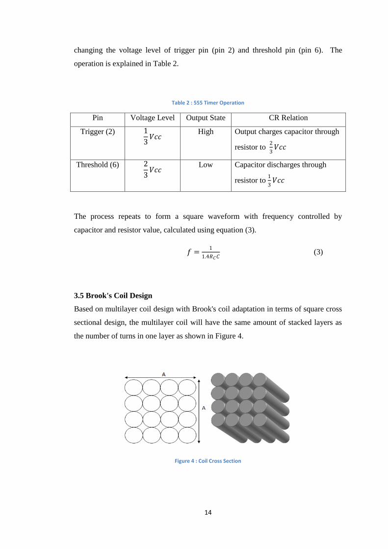
3.5 Brook's Coil Design
Based on multilayer coil design with Brook's coil adaptation in terms of square cross
sectional design, the multilayer coil will have the same amount of stacked layers as
the number of turns in one layer as shown in Figure 4.
Figure 4 : Coil Cross Section

15
This will ensure a square cross sectional area with high inductance, calculated using
equation (4) from [13].
𝐿 =0.8𝑟2𝑁2
6𝑟+9𝑙+10𝑑 (4)
where r = mean radius of coil (inches)
N = number of turns of coil
𝑙 = length of coil (inches)
d = depth of coil (inches)
The coil will use air as the core which avoids magnetic saturation with the material
chosen to have high conductivity and relative permeability that increases magnetic
field strength. Furthermore, a circular coil shape will be designed to provide highest
efficiency.
16
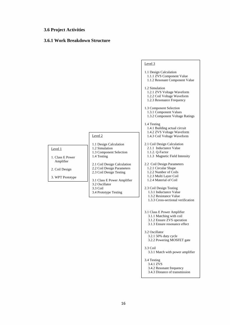
3.6 Project Activities
3.6.1 Work Breakdown Structure
Level 1
1. Class E Power
Amplifier
2. Coil Design
3. WPT Prototype
Level 2
1.1 Design Calculation
1.2 Simulation
1.3 Component Selection
1.4 Testing
2.1 Coil Design Calculation
2.2 Coil Design Parameters
2.3 Coil Design Testing
3.1 Class E Power Amplifier
3.2 Oscillator
3.3 Coil
3.4 Prototype Testing
Level 3
1.1 Design Calculation
1.1.1 ZVS Component Value
1.1.2 Resonant Component Value
1.2 Simulation
1.2.1 ZVS Voltage Waveform
1.2.2 Coil Voltage Waveform
1.2.3 Resonance Frequency
1.3 Component Selection
1.3.1 Component Values
1.3.2 Component Voltage Ratings
1.4 Testing
1.4.1 Building actual circuit
1.4.2 ZVS Voltage Waveform
1.4.3 Coil Voltage Waveform
2.1 Coil Design Calculation
2.1.1 Inductance Value
1.1.2. Q-Factor
1.1.3 Magnetic Field Intensity
2.2 Coil Design Parameters
1.2.1 Circular Shape
1.2.2 Number of Coils
1.2.3 Multi Layer Coil
1.2.4 Material of Coil
2.3 Coil Design Testing
1.3.1 Inductance Value
1.3.2 Resistance Value
1.3.3 Cross-sectional verification
3.1 Class E Power Amplifier
3.1.1 Matching with coil
3.1.2 Ensure ZVS operation
3.1.3 Ensure resonance effect
3.2 Oscillator
3.2.1 50% duty cycle
3.2.2 Powering MOSFET gate
3.3 Coil
3.3.1 Match with power amplifier
3.4 Testing
3.4.1 ZVS
3.4.2 Resonant frequency
3.4.3 Distance of transmission

17
Figure 5 : FYP 1 Gantt Chart

18
Figure 6 : FYP 2 Gantt Chart
19
CHAPTER 4
RESULTS AND DISCUSSION
4.1 Overview
This project will demonstrate results for each section listed from Methodology
covering :
1. Class E Power Amplifier
2. Brook's Coil Design Adaptation
3. Wireless Power Transmission Prototype
The calculation and simulation will be determined with selection of components,
followed by the actual results and discussion obtained for each section. All
simulations are completed using Multisim software from National Instrument while
other equipment used in measuring practical circuits are highlighted at each section.
4.2 Class E Power Amplifier
4.2.1 Simulation
Based on the design concept and calculation covered in methodology, the circuit is
build and simulated before practical application. Figure 7 shows the simulated
circuit connection and component values from calculations.
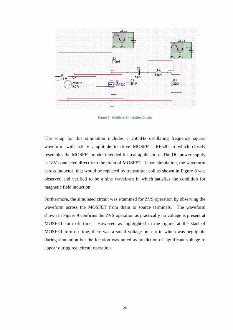
20
Figure 7 : Multisim Simulation Circuit
The setup for this simulation includes a 250kHz oscillating frequency square
waveform with 5.5 V amplitude to drive MOSFET IRF520 in which closely
resembles the MOSFET model intended for real application. The DC power supply
is 18V connected directly to the drain of MOSFET. Upon simulation, the waveform
across inductor that would be replaced by transmitter coil as shown in Figure 8 was
observed and verified to be a sine waveform in which satisfies the condition for
magnetic field induction.
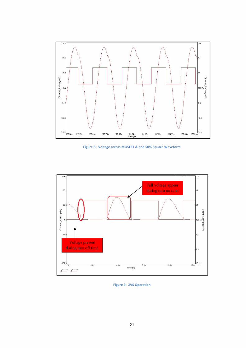
Furthermore, the simulated circuit was examined for ZVS operation by observing the
waveform across the MOSFET from drain to source terminals. The waveform
shown in Figure 9 confirms the ZVS operation as practically no voltage is present at
MOSFET turn off time. However, as highlighted in the figure, at the start of
MOSFET turn on time, there was a small voltage present in which was negligible
during simulation but the location was noted as prediction of significant voltage to
appear during real circuit operation.
21
Figure 8 : Voltage across MOSFET & and 50% Square Waveform
Figure 9 : ZVS Operation
Voltage present
during turn off time
Full voltage appear
during turn on time
22
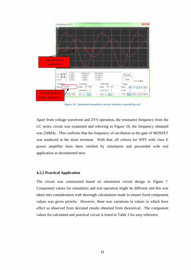
Figure 10 : Simulated waveform across inductor resembling coil
Apart from voltage waveform and ZVS operation, the resonance frequency from the
LC series circuit was examined and referring to Figure 10, the frequency obtained
was 250kHz. This confirms that the frequency of oscillation at the gate of MOSFET
was unaltered at the drain terminal. With that, all criteria for WPT with class E
power amplifier have been verified by simulation and proceeded with real
application as documented next.
4.2.2 Practical Application
The circuit was constructed based on simulation circuit design in Figure 7.
Component values for simulation and real operation might be different and this was
taken into consideration with thorough calculations made to ensure fixed component
values was given priority. However, there was variations in values in which have
effect as observed from deviated results obtained from theoretical. The component
values for calculated and practical circuit is listed in Table 3 for easy reference.
One period of
oscillation
Time/division to
obtain frequency.
23
Table 3 : Calculated & Practical Specification
Description q F(Hz) L1(µH) C1(nF) L2(µH) C2(nF) R(Ω)
Calculated 1.412 250k 9.65 20.2 68.8 5.89 22
Practical 250k 10 20 68 5.6 22
Equipments used in this test are as follows :
1. GW Instek Laboratory DC Power Supply
Used for 18 V DC power supply
2. Tektronix TDS 1002 Digital Oscilloscope
Used for reading voltage waveform
3. GW Instek Function Generator GFG-8256
Used for substituting oscillator circuit to drive MOSFET gate
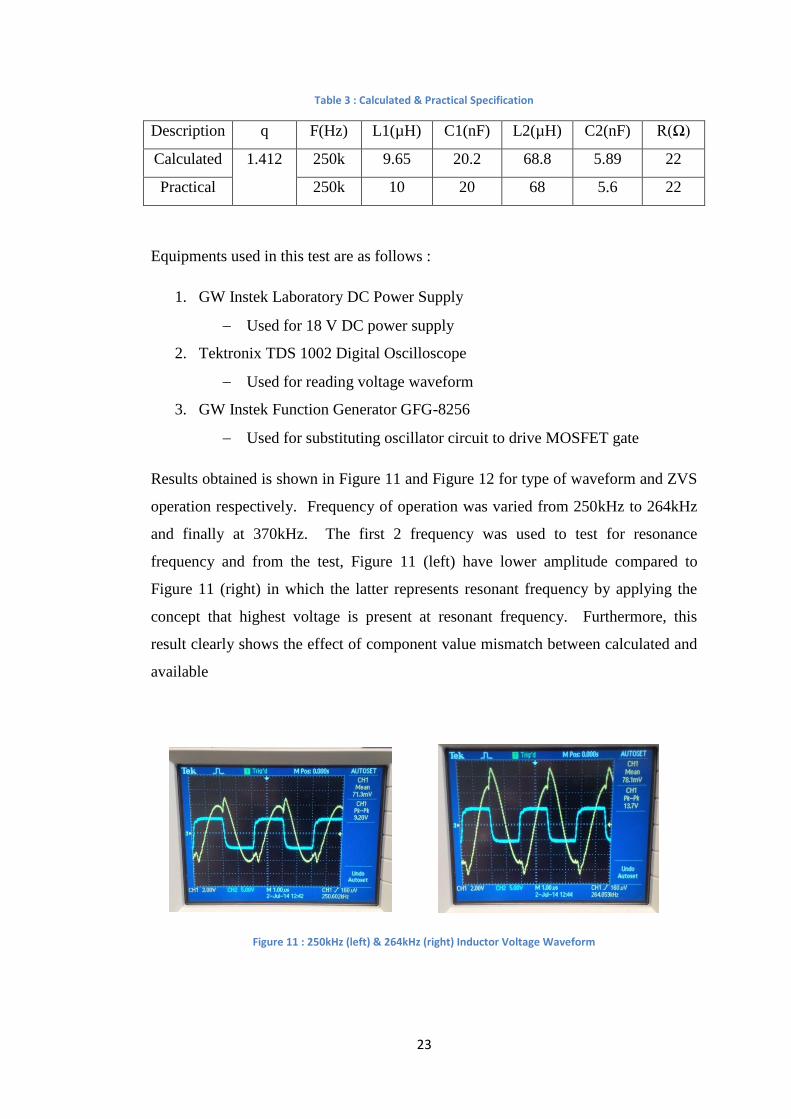
Results obtained is shown in Figure 11 and Figure 12 for type of waveform and ZVS
operation respectively. Frequency of operation was varied from 250kHz to 264kHz
and finally at 370kHz. The first 2 frequency was used to test for resonance
frequency and from the test, Figure 11 (left) have lower amplitude compared to
Figure 11 (right) in which the latter represents resonant frequency by applying the
concept that highest voltage is present at resonant frequency. Furthermore, this
result clearly shows the effect of component value mismatch between calculated and
available
Figure 11 : 250kHz (left) & 264kHz (right) Inductor Voltage Waveform
24
values forms the fact that resonant frequency was affected. Despite the difference,
voltage waveform conforms to simulated results with sine waveform confirmed.
Although there was a distortion at the peak of sine wave due to noise and LC effect
that was not perfect taking consideration in tolerance of component values but this
was similar to simulation and can be neglected since quality of sine waveform is not
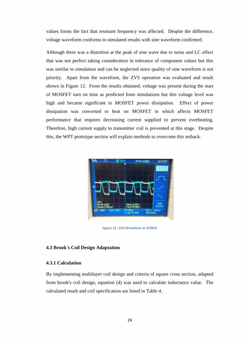
priority. Apart from the waveform, the ZVS operation was evaluated and result
shown in Figure 12. From the results obtained, voltage was present during the start
of MOSFET turn on time as predicted from simulations but this voltage level was
high and became significant to MOSFET power dissipation. Effect of power
dissipation was converted to heat on MOSFET in which affects MOSFET
performance that requires decreasing current supplied to prevent overheating.
Therefore, high current supply to transmitter coil is prevented at this stage. Despite
this, the WPT prototype section will explain methods to overcome this setback.
Figure 12 : ZVS Waveform at 370kHz
4.3 Brook's Coil Design Adaptation
4.3.1 Calculation
By implementing multilayer coil design and criteria of square cross section, adapted
from brook's coil design, equation (4) was used to calculate inductance value. The
calculated result and coil specification are listed in Table 4.
25
Table 4 : Coil Specification
Material Cable
Diameter
(cm)
Coil
Diameter
(cm)
Length/Width of
cross section (cm)
No. of
Turns
Inductance
(µH)
Enamelled
Copper
0.15 8.8 0.7/0.7 16 39
4.3.2 Practical Application
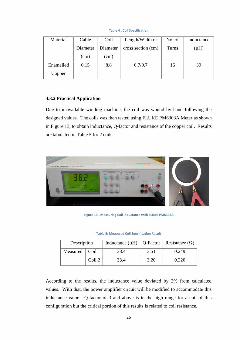
Due to unavailable winding machine, the coil was wound by hand following the
designed values. The coils was then tested using FLUKE PM6303A Meter as shown
in Figure 13, to obtain inductance, Q-factor and resistance of the copper coil. Results
are tabulated in Table 5 for 2 coils.
Figure 13 : Measuring Coil Inductance with FLUKE PM6303A
Table 5: Measured Coil Specification Result
Description Inductance (µH) Q-Factor Resistance (Ω)
Measured Coil 1 38.4 3.51 0.249
Coil 2 33.4 3.20 0.220
According to the results, the inductance value deviated by 2% from calculated
values. With that, the power amplifier circuit will be modified to accommodate this
inductance value. Q-factor of 3 and above is in the high range for a coil of this
configuration but the critical portion of this results is related to coil resistance.
26
Following that the resistance must be low to be insignificant for WPT circuit
performance and since the resistance is below 1 Ω due to multilayer coil design, it is
safe to assume constant performance without distinct effect. Therefore, the coil
design is considered optimum within this project with high inductance and low
resistance. The coil will proceed to implementation in the next section which
demonstrates an air core advantage with current's effect on inductance.
4.4 Wireless Power Transmission Prototype
The wireless power transmission circuit consists of power supply, class E power
amplifier with transmitter and receiver coils. The L2 inductor in class E power
amplifier was replaced with the multilayer Brook's coil and functions as the
transmitter.
Referring to Class E power amplifier section, matching of coil inductance and
resistance with resonance frequency of amplifier circuit was completed. With that,
the resonance frequency was set to 374kHz instead of previous frequency obtained
for class E power amplifier. This frequency configuration was caused by changes in
inductor value from 68µH component to 38µH coil. The frequency setting was
ensured similar between the transmitter and receiver coil that achieved magnetic
resonance coupling system configuration. The same capacitor value is used at both
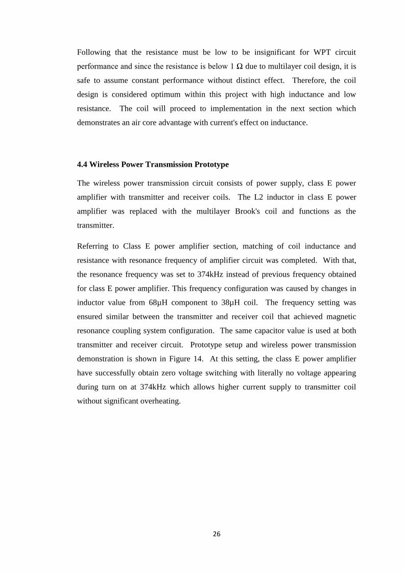
transmitter and receiver circuit. Prototype setup and wireless power transmission
demonstration is shown in Figure 14. At this setting, the class E power amplifier
have successfully obtain zero voltage switching with literally no voltage appearing
during turn on at 374kHz which allows higher current supply to transmitter coil
without significant overheating.
27
Figure 14 : Wireless Power Transmission Demonstration
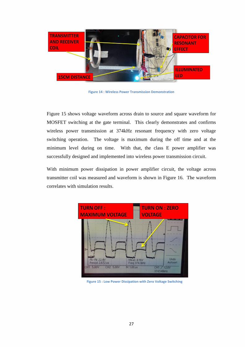
Figure 15 shows voltage waveform across drain to source and square waveform for
MOSFET switching at the gate terminal. This clearly demonstrates and confirms
wireless power transmission at 374kHz resonant frequency with zero voltage
switching operation. The voltage is maximum during the off time and at the
minimum level during on time. With that, the class E power amplifier was
successfully designed and implemented into wireless power transmission circuit.
With minimum power dissipation in power amplifier circuit, the voltage across
transmitter coil was measured and waveform is shown in Figure 16. The waveform
correlates with simulation results.
Figure 15 : Low Power Dissipation with Zero Voltage Switching
28
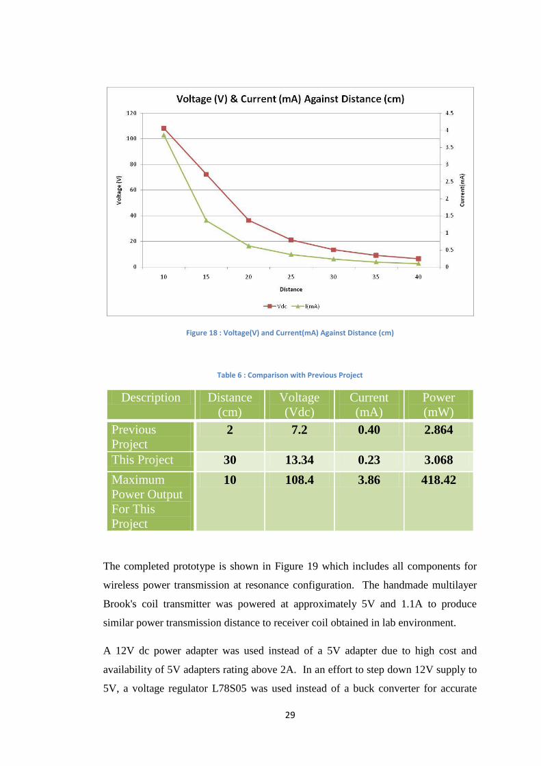
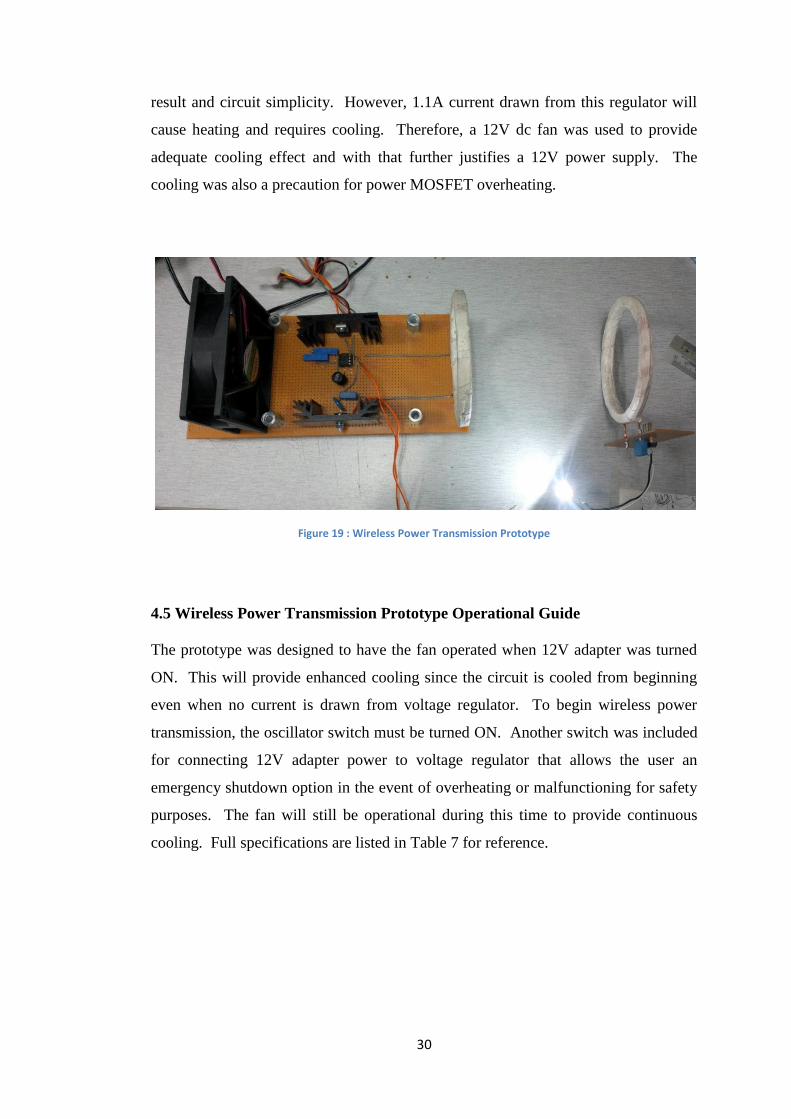
Following that, the voltage and current was measured at receiver side for increasing
distance. Referring to Figure 17, the power at receiver was highest at 10cm apart,
measuring 418.34mW and decreases as distance increases. 108V DC was measured
at 10cm with 3.86mA current which represents the highest achieved output as shown
in Figure 18. In comparison with previous project, the distance was compared at the
same output power level. As shown in Table 6, at the same output power, the
distance of this project was 30cm and signifies an increase of 15 times with previous
project of 2cm distance as reference.
Figure 17 : Graph of Power (mW) against Distance (cm)
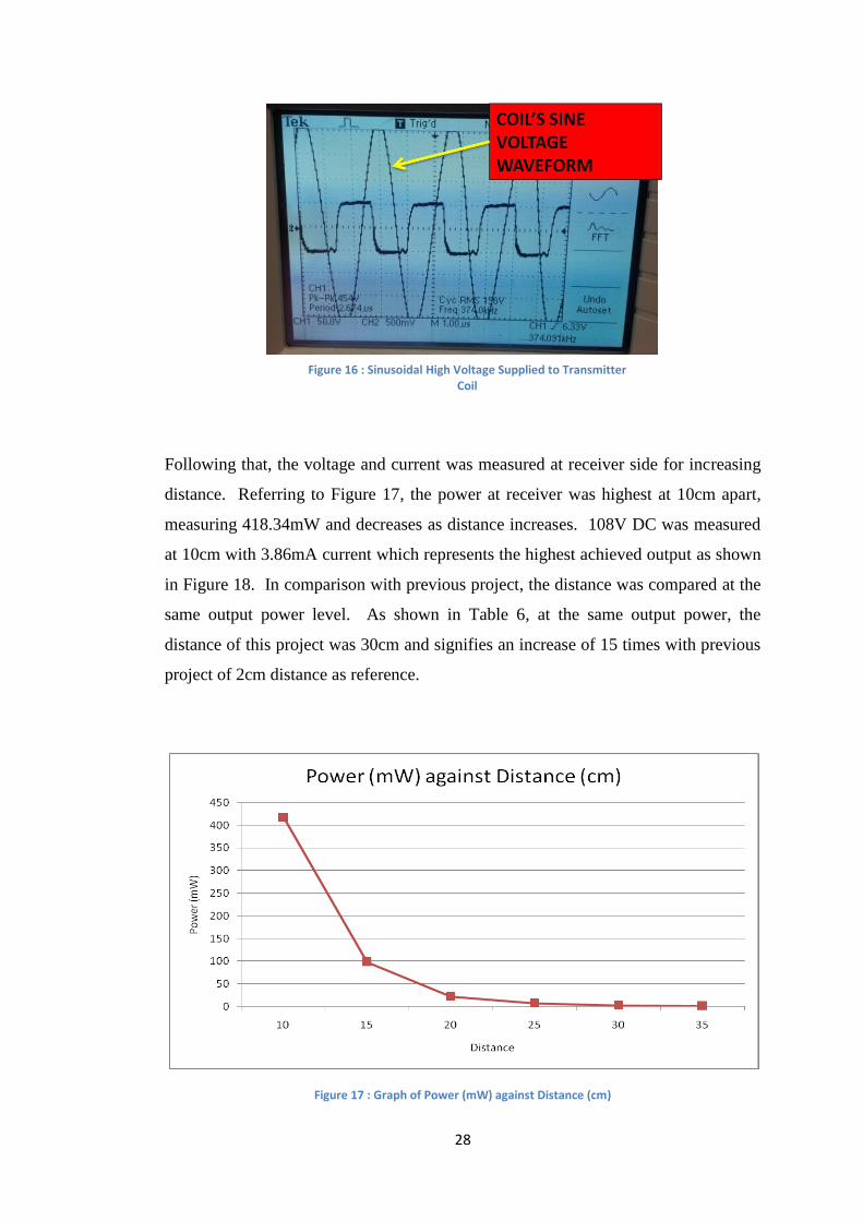
Figure 16 : Sinusoidal High Voltage Supplied to Transmitter Coil
29
Figure 18 : Voltage(V) and Current(mA) Against Distance (cm)
Table 6 : Comparison with Previous Project
Description Distance
(cm)
Voltage
(Vdc)
Current
(mA)
Power
(mW)
Previous
Project 2 7.2 0.40 2.864
This Project 30 13.34 0.23 3.068
Maximum
Power Output
For This
Project
10 108.4 3.86 418.42
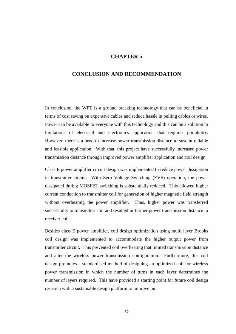
The completed prototype is shown in Figure 19 which includes all components for
wireless power transmission at resonance configuration. The handmade multilayer
Brook's coil transmitter was powered at approximately 5V and 1.1A to produce
similar power transmission distance to receiver coil obtained in lab environment.
A 12V dc power adapter was used instead of a 5V adapter due to high cost and
availability of 5V adapters rating above 2A. In an effort to step down 12V supply to
5V, a voltage regulator L78S05 was used instead of a buck converter for accurate
30
result and circuit simplicity. However, 1.1A current drawn from this regulator will
cause heating and requires cooling. Therefore, a 12V dc fan was used to provide
adequate cooling effect and with that further justifies a 12V power supply. The
cooling was also a precaution for power MOSFET overheating.
Figure 19 : Wireless Power Transmission Prototype
4.5 Wireless Power Transmission Prototype Operational Guide
The prototype was designed to have the fan operated when 12V adapter was turned
ON. This will provide enhanced cooling since the circuit is cooled from beginning
even when no current is drawn from voltage regulator. To begin wireless power
transmission, the oscillator switch must be turned ON. Another switch was included
for connecting 12V adapter power to voltage regulator that allows the user an
emergency shutdown option in the event of overheating or malfunctioning for safety
purposes. The fan will still be operational during this time to provide continuous
cooling. Full specifications are listed in Table 7 for reference.

31
Table 7 : Prototype Technical Specification
Technical Specification Power supply Voltage (VDC) 12
Current (A) 2
Operating Frequency (kHz) 374
Output Power Distance (cm) 10
Power (mW) 418
Fan Rating Voltage (VDC) 12V
Current (A) 0.25
Transmitter Dimension 10 X 15 X 10
Coil
Dimension
Wire Diameter (cm) 0.15
Coil Diameter (cm) 8.8
Cross Sectional Area (cm) 0.7 X 0.7
32
CHAPTER 5
CONCLUSION AND RECOMMENDATION
In conclusion, the WPT is a ground breaking technology that can be beneficial in
terms of cost saving on expensive cables and reduce hassle in pulling cables or wires.
Power can be available to everyone with this technology and this can be a solution to
limitations of electrical and electronics application that requires portability.
However, there is a need to increase power transmission distance to sustain reliable
and feasible application. With that, this project have successfully increased power
transmission distance through improved power amplifier application and coil design.
Class E power amplifier circuit design was implemented to reduce power dissipation
in transmitter circuit. With Zero Voltage Switching (ZVS) operation, the power
dissipated during MOSFET switching is substantially reduced. This allowed higher
current conduction to transmitter coil for generation of higher magnetic field strength
without overheating the power amplifier. Thus, higher power was transferred
successfully to transmitter coil and resulted in further power transmission distance to
receiver coil.
Besides class E power amplifier, coil design optimization using multi layer Brooks
coil design was implemented to accommodate the higher output power from
transmitter circuit. This prevented coil overheating that limited transmission distance
and alter the wireless power transmission configuration. Furthermore, this coil
design promotes a standardised method of designing an optimized coil for wireless
power transmission in which the number of turns in each layer determines the
number of layers required. This have provided a starting point for future coil design
research with a sustainable design platform to improve on.

33
With improved power amplifier application and coil design in this project, an
improvement of 15 times the transmission distance from previous project was
achieved. This clearly defines the feasibility and recognition of class E power
amplifier and multilayer Brook's coil for improving transmission distance of wireless
power transmission via magnetic resonance coupling.
Future improvement is recommended on using different resonant frequency, coil
material and diameter. Future research focused towards increasing power transfer
efficiency with increased distance is advised to design power amplifier with different
frequency range and more enhancement in coil material coupled with magnetic field
effect study on the coil itself. This will prove to increase feasibility of this
technology and widen the scope of application.

34
REFERENCES
[1] J. L. W. Li, "Wireless power transmission: State-of-the-arts in technologies and potential applications (invited paper)," in Microwave Conference Proceedings (APMC), 2011 Asia-Pacific, 2011, pp. 86-89.
[2] A. Kurs, A. Karalis, R. Moffatt, J. D. Joannopoulos, P. Fisher, and M. Soljacic, "Wireless Power Transfer via Strongly Coupled Magnetic Resonances," Science Express, vol. 317, pp. 83-86, 2007.
[3] W. Qiang and L. Hong, "Research on the wireless power transmission system based on coupled magnetic resonances," in Electronics, Communications and Control (ICECC), 2011 International Conference on, 2011, pp. 2255-2258.
[4] M. Dionigi and M. Mongiardo, "Magnetically coupled resonant Wireless Power Transmission systems with relay elements," in Microwave Workshop Series on Innovative Wireless Power Transmission: Technologies, Systems, and Applications (IMWS), 2012 IEEE MTT-S International, 2012, pp. 223-226.
[5] K. Seong-Min, I. K. Cho, J. I. Moon, S. I. Jeon, and J. I. Choi, "5W wireless power transmission system with coupled magnetic resonance," in Microwave, Antenna, Propagation and EMC Technologies for Wireless Communications (MAPE), 2013 IEEE 5th International Symposium on, 2013, pp. 255-258.
[6] Y. Kawamura and M. Shoyama, "Wireless power transmission using LC cancellation," in ECCE Asia Downunder (ECCE Asia), 2013 IEEE, 2013, pp. 1041-1045.
[7] A. E. Gundogdu and E. Afacan, "Some experiments related to wireless power transmission," in Cross Strait Quad-Regional Radio Science and Wireless Technology Conference (CSQRWC), 2011, 2011, pp. 507-509.
[8] M. Kovic, "Investigating technology transfer projects and institutional development in developing countries," Management of Environmental Quality: An International Journal, vol. 21, pp. 761-772, 2010.
[9] P. Jae-Hyun, P. Byung-Chul, L. Jeong-Hae, R. Young-Ho, P. Eun-Seok, and K. Sang-Wook, "Optimum frequency of high Q-factor resonator for magnetic resonance coupling," in Microwave Conference (EuMC), 2011 41st European, 2011, pp. 61-63.
[10] J. Bing, J. R. Smith, M. Philipose, S. Roy, K. Sundara-Rajan, and A. V. Mamishev, "Energy Scavenging for Inductively Coupled Passive RFID Systems," in Instrumentation and Measurement Technology Conference, 2005. IMTC 2005. Proceedings of the IEEE, 2005, pp. 984-989.
[11] K. Tashiro, H. Wakiwaka, S. Inoue, and Y. Uchiyama, "Energy Harvesting of Magnetic Power-Line Noise," Magnetics, IEEE Transactions on, vol. 47, pp. 4441-4444, 2011.
[12] M. Takato, T. Nishi, M. Kaneko, J. Tanida, S. Tada, K. Saito, et al., "Multilayer ceramic coil for wireless power transfer system by photo resist film process," in Electronics Packaging (ICEP), 2014 International Conference on, 2014, pp. 326-331.
[13] B. H. Soong, Y. L. Sum, W. Liu, and S. Ramachandran, "Characterizing wire wound inductor coils for optimized wireless power transfer," in Advanced Intelligent Mechatronics, 2009. AIM 2009. IEEE/ASME International Conference on, 2009, pp. 469-474.
[14] N. S. Artan, R. C. Patel, N. Chengzhi, and H. J. Chao, "High-efficiency wireless power delivery for medical implants using hybrid coils," in Engineering in Medicine and Biology Society (EMBC), 2012 Annual International Conference of the IEEE, 2012, pp. 1683-1686.

35
[15] K. Tashiro, "Broadband Air-Core Brooks-Coil Induction Magnetometer," in SICE-ICASE, 2006. International Joint Conference, 2006, pp. 179-182.
[16] N. O. Sokal and A. D. Sokal, "Class E-A new class of high-efficiency tuned single-ended switching power amplifiers," Solid-State Circuits, IEEE Journal of, vol. 10, pp. 168-176, 1975.
[17] M. Acar, A. J. Annema, and B. Nauta, "Generalized Design Equations for Class-E Power Amplifiers with Finite DC Feed Inductance," in Microwave Conference, 2006. 36th European, 2006, pp. 1308-1311.
[18] R. A. C. Wei-Ting Chen, Shuhei Yoshida, Jenshan Lin, and Chao-Kai Hsu, "A 36W Wireless Power Transfer System with 82% Efficiency for LED Lighting Applications," The Japan Institute of Electronics Packaging vol. 6, pp. 32-36, 2013.
[19] W. Chen, R. A. Chinga, S. Yoshida, J. Lin, C. Chen, and W. Lo, "A 25.6 W 13.56 MHz wireless power transfer system with a 94% efficiency GaN Class-E power amplifier," in Microwave Symposium Digest (MTT), 2012 IEEE MTT-S International, 2012, pp. 1-3.