Embed Size (px)
Citation preview

Ultra Low-Power Codec for Portable Audio Applications
http://www.cirrus.com
Copyright Cirrus Logic, Inc., 2009–2016
(All Rights Reserved)
Rev 4.0
DEC ‘16
WM8904
DESCRIPTION
The WM8904 is a high performance ultra-low power stereo
CODEC optimised for portable audio applications.
The device features stereo ground-referenced headphone
amplifiers using the Wolfson ‘Class-W’ amplifier techniques -
incorporating an innovative dual-mode charge pump
architecture - to optimise efficiency and power consumption
during playback. The ground-referenced headphone and line
outputs eliminate AC coupling capacitors, and both outputs
include common mode feedback paths to reject ground
noise.
Control sequences for audio path setup can be pre-loaded
and executed by an integrated control write sequencer to
reduce software driver development and minimise pops and
clicks via SilentSwitch™ technology.
The analogue input stage can be configured for single
ended or differential inputs. Up to 3 stereo microphone or
line inputs may be connected. The input impedance is
constant with PGA gain setting.
A stereo digital microphone interface is provided, with a
choice of two inputs.
A dynamic range controller provides compression and level
control to support a wide range of portable recording
applications. Anti-clip and quick release features offer good
performance in the presence of loud impulsive noises.
ReTuneTM Mobile 5-band parametric equaliser with fully
programmable coefficients is integrated for optimization of
speaker characteristics. Programmable dynamic range
control is also available for maximizing loudness, protecting
speakers from clipping and preventing premature shutdown
due to battery droop.
Common audio sampling frequencies are supported from a
wide range of external clocks, either directly or generated
via the FLL.
The WM8904 can operate directly from a single 1.8V
switched supply. For optimal power consumption, the digital
core can be operated from a 1.0V supply.
FEATURES
3.0mW quiescent power consumption for DAC to
headphone playback
DAC SNR 96dB typical, THD -86dB typical
ADC SNR 91dB typical, THD -80dB typical
2.4mW quiescent power consumption for analogue bypass
playback
Control write sequencer for pop minimised start-up and
shutdown
Single register write for default start-up sequence
Integrated FLL provides all necessary clocks
- Self-clocking modes allow processor to sleep
- All standard sample rates from 8kHz to 96kHz
Stereo digital microphone input
3 single ended inputs per stereo channel
1 fully differential mic / line input per stereo channel
Digital Dynamic Range Controller (compressor / limiter)
Digital sidetone mixing
Ground-referenced headphone driver
Ground-referenced line outputs
32-pin QFN package (4 x 4mm, 0.4mm pitch)
36-ball WLCSP package (2.6 x 2.5mm, 6 x 6 ball grid,
0.4mm pitch)
APPLICATIONS
Portable multimedia players
Multimedia handsets
Handheld gaming
Wireless headsets
Mobile internet devices
Netbooks

WM8904
2 Rev 4.0
BLOCK DIAGRAM
CONTROL
INTERFACE
AUDIO
INTERFACE
TDM SUPPORT
AD
CD
AT
BC
LK
/ GP
IO4
DA
CD
AT
LR
CL
K
CPVOUTP
CP
GN
D
CP
CA
CPVOUTN
CP
CB
MC
LK
FLL /
CLOCK
CIRCUITRYIR
Q/G
PIO
1
GP
IO2
*
CLASS-W GROUND-
REFERENCED OUTPUTS
MICBIAS
VM
IDC
AG
ND
LINEOUTL
LINEOUTR
LINEOUTFB
HPOUTL
HPOUTR
HPOUTFB
ADAPTIVE
CHARGE PUMP
GP
IO3
*
WM8904
Ground-referenced
Class-W
10
0n
F2
0Ω
10
0n
F2
0Ω
2.2µF
2.2
µF
2.2
µF
2.2
µF
CP
VD
D
4.7
µF
10
0n
F2
0Ω
10
0n
F2
0Ω
4.7
µF
10
0n
F
4.7
µF
AV
DD
MICVDD
DG
ND
DC
VD
D
DB
VD
D
BY
PA
SS
L
M
U
X
M
U
X
M
U
X
M
U
X
BY
PA
SS
R
DA
C L
DA
C R
DYNAMIC RANGE CONTROLLER
(DRC)
5-BAND EQUALISER
DIGITAL MONO MIX
DIGITAL SIDE TONE MIXING
DIGITAL VOLUME CONTROL
ADC
ADC
PGA
PGA
DE
CIM
AT
ION
FIL
TE
RS
INT
ER
PO
LA
TIO
N F
ILT
ER
S
DAC
DIGITAL MIC
INTERFACE
DAC
M
U
X
IN1L/DMICDAT1
IN2L
IN3L*1µF
M
U
X1µF
IN1R/DMICDAT2
IN2R
IN3R*
SD
A
SC
LK
VMID
Reference
10
0n
F
10
0n
F
Note:
* these pins are not available in
the 32-pin QFN package variant

WM8904
Rev 4.0 3
TABLE OF CONTENTS
DESCRIPTION ................................................................................................................ 1
FEATURES ..................................................................................................................... 1
APPLICATIONS .............................................................................................................. 1
BLOCK DIAGRAM ......................................................................................................... 2
TABLE OF CONTENTS .................................................................................................. 3
AUDIO SIGNAL PATHS DIAGRAM ............................................................................... 6
PIN CONFIGURATION ................................................................................................... 7
ORDERING INFORMATION ........................................................................................... 8
PIN DESCRIPTION ......................................................................................................... 9
ABSOLUTE MAXIMUM RATINGS ............................................................................... 10
RECOMMENDED OPERATING CONDITIONS ............................................................ 10
ELECTRICAL CHARACTERISTICS ............................................................................ 11 TERMINOLOGY ...................................................................................................................... 11 COMMON TEST CONDITIONS .............................................................................................. 11 INPUT SIGNAL PATH ............................................................................................................. 12 OUTPUT SIGNAL PATH ......................................................................................................... 16 BYPASS PATH ........................................................................................................................ 18 CHARGE PUMP ...................................................................................................................... 18 FLL .......................................................................................................................................... 18 OTHER PARAMETERS .......................................................................................................... 19
POWER CONSUMPTION ............................................................................................. 21 COMMON TEST CONDITIONS .............................................................................................. 21 POWER CONSUMPTION MEASUREMENTS ........................................................................ 21
SIGNAL TIMING REQUIREMENTS ............................................................................. 25 COMMON TEST CONDITIONS .............................................................................................. 25 MASTER CLOCK .................................................................................................................... 25 AUDIO INTERFACE TIMING .................................................................................................. 26
MASTER MODE .......................................................................................................................................................................... 26 SLAVE MODE .............................................................................................................................................................................. 27 TDM MODE ................................................................................................................................................................................. 28
CONTROL INTERFACE TIMING ............................................................................................ 29
DIGITAL FILTER CHARACTERISTICS ....................................................................... 30 ADC FILTER RESPONSES .................................................................................................... 31 ADC HIGH PASS FILTER RESPONSES ................................................................................ 31 DAC FILTER RESPONSES .................................................................................................... 32 DE-EMPHASIS FILTER RESPONSES ................................................................................... 33
DEVICE DESCRIPTION ............................................................................................... 34 INTRODUCTION ..................................................................................................................... 34 ANALOGUE INPUT SIGNAL PATH ........................................................................................ 35
INPUT PGA ENABLE .................................................................................................................................................................. 36 INPUT PGA CONFIGURATION................................................................................................................................................... 36 SINGLE-ENDED INPUT .............................................................................................................................................................. 38 DIFFERENTIAL LINE INPUT ....................................................................................................................................................... 38 DIFFERENTIAL MICROPHONE INPUT ...................................................................................................................................... 39 INPUT PGA GAIN CONTROL ..................................................................................................................................................... 39 INPUT PGA COMMON MODE AMPLIFIER ................................................................................................................................ 41
ELECTRET CONDENSER MICROPHONE INTERFACE ....................................................... 42 MICBIAS CONTROL .................................................................................................................................................................... 42

WM8904
4 Rev 4.0
MICBIAS CURRENT DETECT .................................................................................................................................................... 43 MICBIAS CURRENT DETECT FILTERING ................................................................................................................................ 43 MICROPHONE HOOK SWITCH DETECTION ............................................................................................................................ 45
DIGITAL MICROPHONE INTERFACE .................................................................................... 46 ANALOGUE-TO-DIGITAL CONVERTER (ADC) ..................................................................... 47
ADC DIGITAL VOLUME CONTROL ............................................................................................................................................ 48 HIGH PASS FILTER .................................................................................................................................................................... 50 ADC OVERSAMPLING RATIO (OSR) ........................................................................................................................................ 51
DYNAMIC RANGE CONTROL (DRC) ..................................................................................... 51 COMPRESSION/LIMITING CAPABILITIES ................................................................................................................................ 52 GAIN LIMITS ................................................................................................................................................................................ 53 DYNAMIC CHARACTERISTICS ................................................................................................................................................. 54 ANTI-CLIP CONTROL ................................................................................................................................................................. 54 QUICK RELEASE CONTROL ..................................................................................................................................................... 55 GAIN SMOOTHING ..................................................................................................................................................................... 56 INITIALISATION .......................................................................................................................................................................... 56
RETUNETM MOBILE PARAMETRIC EQUALIZER (EQ) .......................................................... 57 DEFAULT MODE (5-BAND PARAMETRIC EQ) ......................................................................................................................... 57 RETUNETM MOBILE MODE ......................................................................................................................................................... 58 EQ FILTER CHARACTERISTICS ............................................................................................................................................... 58
DIGITAL MIXING ..................................................................................................................... 60 DIGITAL MIXING PATHS ............................................................................................................................................................ 60 DAC INTERFACE VOLUME BOOST .......................................................................................................................................... 62 DIGITAL SIDETONE .................................................................................................................................................................... 62
DIGITAL-TO-ANALOGUE CONVERTER (DAC) ..................................................................... 64 DAC DIGITAL VOLUME CONTROL ............................................................................................................................................ 64 DAC SOFT MUTE AND SOFT UN-MUTE ................................................................................................................................... 66 DAC MONO MIX .......................................................................................................................................................................... 67 DAC DE-EMPHASIS .................................................................................................................................................................... 67 DAC SLOPING STOPBAND FILTER .......................................................................................................................................... 68 DAC OVERSAMPLING RATIO (OSR) ........................................................................................................................................ 68
OUTPUT SIGNAL PATH ......................................................................................................... 69 OUTPUT SIGNAL PATHS ENABLE ............................................................................................................................................ 70 HEADPHONE / LINE OUTPUT SIGNAL PATHS ENABLE ......................................................................................................... 70 OUTPUT MUX CONTROL ........................................................................................................................................................... 73 OUTPUT VOLUME CONTROL.................................................................................................................................................... 74
ANALOGUE OUTPUTS ........................................................................................................... 76 HEADPHONE OUTPUTS – HPOUTL AND HPOUTR ................................................................................................................. 76 LINE OUTPUTS – LINEOUTL AND LINEOUTR.......................................................................................................................... 76 EXTERNAL COMPONENTS FOR GROUND REFERENCED OUTPUTS .................................................................................. 77
REFERENCE VOLTAGES AND MASTER BIAS ..................................................................... 77 ANALOGUE REFERENCE AND MASTER BIAS ........................................................................................................................ 77 LOW POWER PLAYBACK MODE .............................................................................................................................................. 79
POP SUPPRESSION CONTROL ............................................................................................ 80 DISABLED INPUT CONTROL ..................................................................................................................................................... 80
CHARGE PUMP ...................................................................................................................... 80 DC SERVO .............................................................................................................................. 82
DC SERVO ENABLE AND START-UP ....................................................................................................................................... 82 DC SERVO ACTIVE MODES ...................................................................................................................................................... 85 DC SERVO READBACK ............................................................................................................................................................. 87
DIGITAL AUDIO INTERFACE ................................................................................................. 87 MASTER AND SLAVE MODE OPERATION ............................................................................................................................... 87 OPERATION WITH TDM ............................................................................................................................................................. 88 BCLK FREQUENCY .................................................................................................................................................................... 89 AUDIO DATA FORMATS (NORMAL MODE) .............................................................................................................................. 89

WM8904
Rev 4.0 5
AUDIO DATA FORMATS (TDM MODE)...................................................................................................................................... 91 DIGITAL AUDIO INTERFACE CONTROL............................................................................... 93
AUDIO INTERFACE OUTPUT TRI-STATE ................................................................................................................................. 94 BCLK AND LRCLK CONTROL .................................................................................................................................................... 94 COMPANDING ............................................................................................................................................................................ 95 LOOPBACK ................................................................................................................................................................................. 97 DIGITAL PULL-UP AND PULL-DOWN ........................................................................................................................................ 97
CLOCKING AND SAMPLE RATES ......................................................................................... 98 SYSCLK CONTROL .................................................................................................................................................................. 100 CONTROL INTERFACE CLOCKING ........................................................................................................................................ 100 CLOCKING CONFIGURATION ................................................................................................................................................. 101 ADC / DAC CLOCK CONTROL ................................................................................................................................................. 102 OPCLK CONTROL .................................................................................................................................................................... 102 TOCLK CONTROL .................................................................................................................................................................... 103 ADC / DAC OPERATION AT 88.2K / 96K ................................................................................................................................. 103
FREQUENCY LOCKED LOOP (FLL) .................................................................................... 104 FREE-RUNNING FLL CLOCK ................................................................................................................................................... 109 GPIO OUTPUTS FROM FLL ..................................................................................................................................................... 109 EXAMPLE FLL CALCULATION ................................................................................................................................................. 110 EXAMPLE FLL SETTINGS ........................................................................................................................................................ 111
GENERAL PURPOSE INPUT/OUTPUT (GPIO) ................................................................... 112 IRQ/GPIO1 ................................................................................................................................................................................. 112 GPIO2 ........................................................................................................................................................................................ 113 GPIO3 ........................................................................................................................................................................................ 113 BCLK/GPIO4 .............................................................................................................................................................................. 114
INTERRUPTS ........................................................................................................................ 115 USING IN1L AND IN1R AS INTERRUPT INPUTS .................................................................................................................... 119
CONTROL INTERFACE ........................................................................................................ 120 CONTROL WRITE SEQUENCER ......................................................................................... 122
INITIATING A SEQUENCE ........................................................................................................................................................ 122 PROGRAMMING A SEQUENCE .............................................................................................................................................. 123 DEFAULT SEQUENCES ........................................................................................................................................................... 126 START-UP SEQUENCE ............................................................................................................................................................ 126 SHUTDOWN SEQUENCE ......................................................................................................................................................... 128
POWER-ON RESET .............................................................................................................. 129 QUICK START-UP AND SHUTDOWN .................................................................................. 131
QUICK START-UP (DEFAULT SEQUENCE) ............................................................................................................................ 131 FAST START-UP FROM STANDBY ......................................................................................................................................... 132 QUICK SHUTDOWN (DEFAULT SEQUENCE)......................................................................................................................... 133
SOFTWARE RESET AND CHIP ID ....................................................................................... 133
REGISTER MAP ......................................................................................................... 134 REGISTER BITS BY ADDRESS ........................................................................................... 138
APPLICATIONS INFORMATION ............................................................................... 177 RECOMMENDED EXTERNAL COMPONENTS ................................................................... 177 MIC DETECTION SEQUENCE USING MICBIAS CURRENT ............................................... 179
PACKAGE DIMENSIONS ........................................................................................... 181
IMPORTANT NOTICE ................................................................................................ 183
REVISION HISTORY .................................................................................................. 184
WM8904
6 Rev 4.0
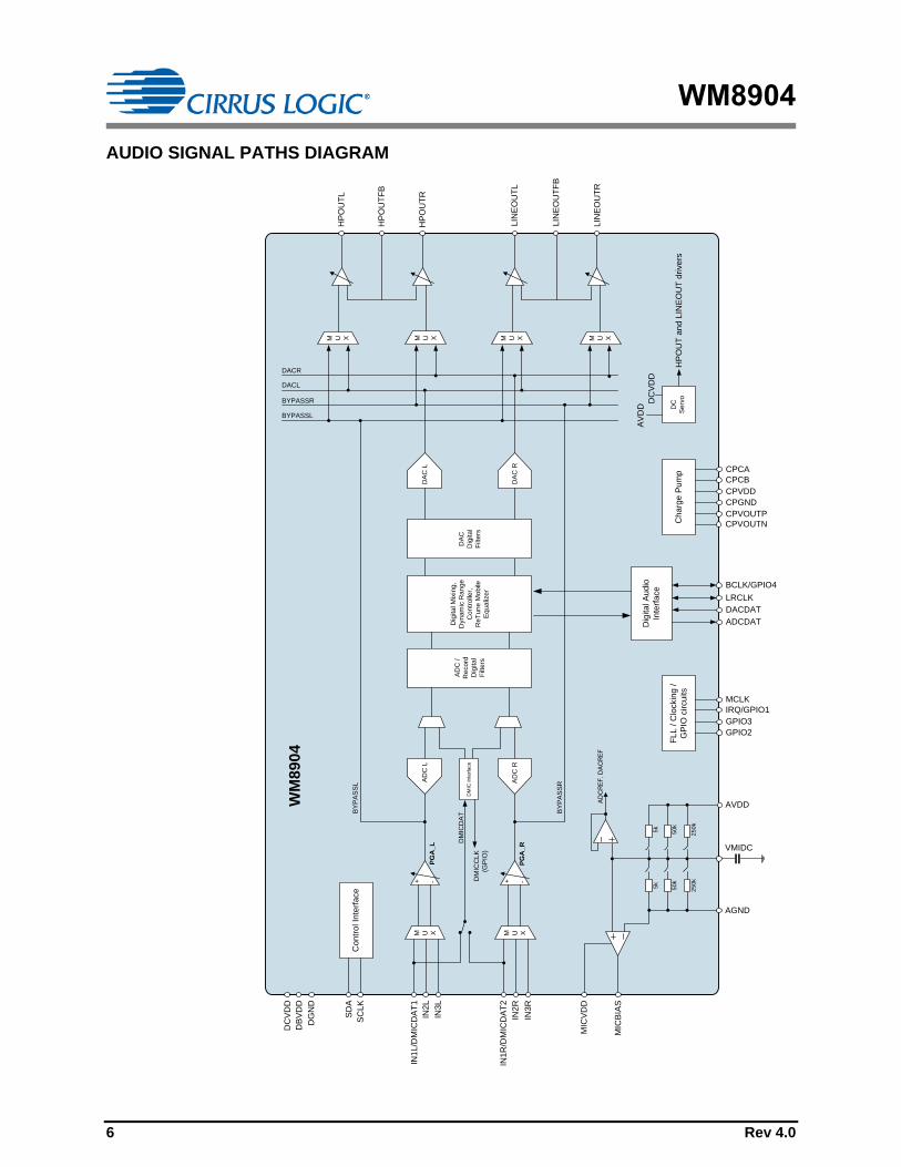
AUDIO SIGNAL PATHS DIAGRAM
IN1
L/D
MIC
DA
T1
IN3
L
IN2
L
IN1
R/D
MIC
DA
T2
IN3
R
IN2
R
HP
OU
TL
HP
OU
TF
B
Ch
arg
e P
um
p
CPVDD
CPGND
CPVOUTP
CPCB
CPCA
CPVOUTN
HP
OU
TR
DC
Se
rvo
AV
DD
DC
VD
D
HP
OU
T a
nd
LIN
EO
UT
drive
rs
BY
PA
SS
L
BY
PA
SS
R
LIN
EO
UT
L
LIN
EO
UT
FB
LIN
EO
UT
R
M U X M U XM U X M U X
BYPASSL
BYPASSR
DACL
DACR
DM
IC in
terf
ace
Dig
ita
l M
ixin
g,
Dyn
am
ic R
an
ge
Co
ntr
olle
r,
Re
Tu
ne
Mo
bile
Eq
ua
lize
r
DA
C
Dig
ita
l
Filt
ers
DA
C R
DA
C L
Dig
ita
l A
ud
io
Inte
rfa
ce
DACDAT
ADCDAT
LRCLK
BCLK/GPIO4
AVDD
AGND
VMIDC
AD
CR
EF, D
AC
REF
DM
ICC
LK
(GP
IO)
DM
ICD
AT
M U XP
GA
_L
-+
AD
C L
M U XP
GA
_R
-+
AD
C R
AD
C /
Re
co
rd
Dig
ita
l
Filt
ers
5k
5k
50k
50
k
25
0k
25
0k
MIC
BIA
S
MIC
VD
D
Co
ntr
ol In
terf
ace
SD
A
SC
LK
FL
L / C
lockin
g /
GP
IO c
ircu
its
GPIO3
GPIO2
IRQ/GPIO1
MCLK
DC
VD
D
DG
ND
DB
VD
DW
M8
90
4

WM8904
Rev 4.0 7
PIN CONFIGURATION
The WM8904 is supplied in a 32-pin QFN package or in a 36-ball CSP format.
The diagram below shows the 32-pin QFN configuration.
CP
VO
UT
N
CP
GN
D
CP
VO
UT
P
CP
CB
IN1R
/DM
ICD
AT
2
IN2L
DA
CD
AT
LR
CL
K
IN1L/D
MIC
DA
T1
HP
OU
TL
HP
OU
TF
B
HP
OU
TR
AD
CD
AT
AGND
LIN
EO
UT
L
LINEOUTFB
IN2R
2526272829303132
1
2
3
4
5
6
7
8
161514131211109
24
23
22
21
20
19
18
17
IRQ/GPIO1
SCLK
SDA
DBVDD
DGND
DCVDD
CPVDD
CPCA
LINEOUTR
MICVDD
MICBIAS
VMIDC
AVDD
MC
LK
BC
LK
/GP
IO4
WM8904
The following diagram shows the 36-ball CSP configuration.
CPVDDHPOUTR
DBVDD
SCLK
VMIDC
AGND
DCVDD
MICVDD
GPIO1/
IRQ
SDA DGNDMICBIAS
BCLK/
GPIO4
MCLKIN2L
IN1R/
DMICDAT
2
DACDATLRCLK
IN1L/
DMICDAT
1
GPIO3
IN2R
CPGND
CPVOUT
P
LINEOUT
L
HPOUTL
CPCBCPVOUT
N
HPOUT
FB
CPCA
ADCDATGPIO2
IN3L
AVDD
IN3R
LINEOUT
FB
LINEOUT
R
1 65432
A
F
E
D
C
B
TOP VIEW – WM8904

WM8904
8 Rev 4.0
ORDERING INFORMATION
DEVICE TEMPERATURE
RANGE PACKAGE
MOISTURE
SENSITIVITY
LEVEL
PEAK
SOLDERING
TEMPERATURE
WM8904CGEFL/V -40°C to +85°C 32-lead QFN
(4 x 4 x 0.75mm, 0.4mm pitch, lead-free)
MSL3 260°C
WM8904CGEFL/RV -40°C to +85°C 32-lead QFN
(4 x 4 x 0.75mm, 0.4mm pitch,
lead-free, tape and reel)
MSL3 260°C
WM8904ECS/R -40°C to +85°C 36-ball W-CSP
(2.6 x 2.5 x 0.5mm, 6 x 6 ball grid,
0.4mm pitch, lead-free, tape and reel)
MSL1 260°C
Note:
QFN Reel quantity = 3,500
W-CSP Reel quantity = 3,500

WM8904
Rev 4.0 9
PIN DESCRIPTION
NAME WLCSP 6×6 QFN-32 TYPE DESCRIPTION
IN1L / DMICDAT1 B3 27 Analogue / Digital Input Left channel input 1 /
Digital microphone data input 1
IN2L A2 26 Analogue Input Left channel input 2
IN3L C3 n/a Analogue Input Left channel input 3
IN1R / DMICDAT2 A1 25 Analogue / Digital Input Right channel input 1 /
Digital microphone data input 2
IN2R B2 24 Analogue Input Right channel input 2
IN3R C2 n/a Analogue Input Right channel input 3
MICBIAS D1 20 Analogue Output Microphone bias
MICVDD E1 19 Supply Microphone bias amp supply
HPOUTL E3 13 Analogue Output Left headphone output (line or headphone
output)
HPOUTR E2 15 Analogue Output Right headphone output (line or headphone
output)
HPOUTFB F3 14 Analogue Input Headphone output ground loop noise rejection
feedback
LINEOUTL F2 16 Analogue Output Left line output 1 (line output)
LINEOUTR F1 18 Analogue Output Right line output 1 (line output)
LINEOUTFB D2 17 Analogue Input Line output ground loop noise rejection
feedback
CPVDD E6 7 Supply Charge pump power supply
CPGND F6 9 Supply Charge pump ground
CPCA E5 8 Analogue Output Charge pump flyback capacitor pin
CPCB F5 10 Analogue Output Charge pump flyback capacitor pin
CPVOUTP E4 11 Analogue Output Charge pump positive supply decoupling
(powers HPOUTL/R, LINEOUTL/R)
CPVOUTN F4 12 Analogue Output Charge pump negative supply decoupling
(powers HPOUTL/R, LINEOUTL/R)
AVDD B1 23 Supply Analogue power supply (powers analogue
inputs, reference, ADC, DAC)
AGND C1 22 Supply Analogue power return
VMIDC D3 21 Midrail voltage decoupling capacitor
DCVDD D5 6 Supply Digital core supply
DBVDD C6 4 Supply Digital buffer supply (powers audio interface
and control interface)
DGND D6 5 Supply Digital ground (return path for DCVDD and
DBVDD)
MCLK A4 28 Digital Input Master clock for CODEC
BCLK / GPIO4 C4 29 Digital Input / Output Audio interface bit clock / GPIO4
LRCLK A5 30 Digital Input / Output Audio interface left / right clock (common for
ADC and DAC)
DACDAT A6 32 Digital Input DAC digital audio data
ADCDAT B5 31 Digital Output ADC digital audio data
SCLK B6 2 Digital Input Control interface clock input
SDA D4 3 Digital Input / Output Control interface data input / output
GPIO1 / IRQ C5 1 Digital Input / Output GPIO1 / Interrupt
GPIO2 B4 n/a Digital Input / Output GPIO2
GPIO3 A3 n/a Digital Input / Output GPIO3
GND_PADDLE n/a 33 Die Paddle
Note:
1. It is recommended that the QFN ground paddle is connected to analogue ground on the application PCB.
WM8904
10 Rev 4.0
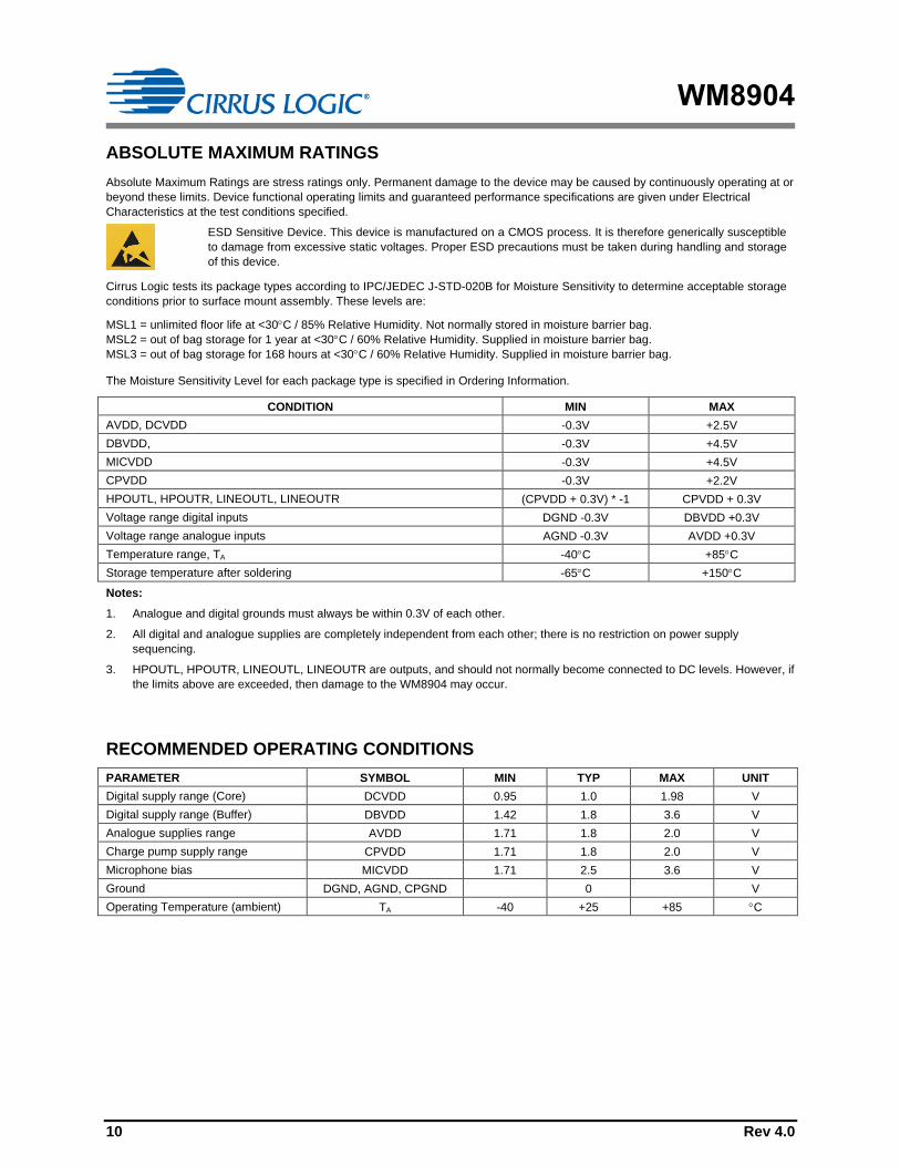
ABSOLUTE MAXIMUM RATINGS
Absolute Maximum Ratings are stress ratings only. Permanent damage to the device may be caused by continuously operating at or
beyond these limits. Device functional operating limits and guaranteed performance specifications are given under Electrical
Characteristics at the test conditions specified.
ESD Sensitive Device. This device is manufactured on a CMOS process. It is therefore generically susceptible
to damage from excessive static voltages. Proper ESD precautions must be taken during handling and storage
of this device.
Cirrus Logic tests its package types according to IPC/JEDEC J-STD-020B for Moisture Sensitivity to determine acceptable storage
conditions prior to surface mount assembly. These levels are:
MSL1 = unlimited floor life at <30C / 85% Relative Humidity. Not normally stored in moisture barrier bag.
MSL2 = out of bag storage for 1 year at <30C / 60% Relative Humidity. Supplied in moisture barrier bag.
MSL3 = out of bag storage for 168 hours at <30C / 60% Relative Humidity. Supplied in moisture barrier bag.
The Moisture Sensitivity Level for each package type is specified in Ordering Information.
CONDITION MIN MAX
AVDD, DCVDD -0.3V +2.5V
DBVDD, -0.3V +4.5V
MICVDD -0.3V +4.5V
CPVDD -0.3V +2.2V
HPOUTL, HPOUTR, LINEOUTL, LINEOUTR (CPVDD + 0.3V) * -1 CPVDD + 0.3V
Voltage range digital inputs DGND -0.3V DBVDD +0.3V
Voltage range analogue inputs AGND -0.3V AVDD +0.3V
Temperature range, TA -40C +85C
Storage temperature after soldering -65C +150C
Notes:
1. Analogue and digital grounds must always be within 0.3V of each other.
2. All digital and analogue supplies are completely independent from each other; there is no restriction on power supply
sequencing.
3. HPOUTL, HPOUTR, LINEOUTL, LINEOUTR are outputs, and should not normally become connected to DC levels. However, if
the limits above are exceeded, then damage to the WM8904 may occur.
RECOMMENDED OPERATING CONDITIONS
PARAMETER SYMBOL MIN TYP MAX UNIT
Digital supply range (Core) DCVDD 0.95 1.0 1.98 V
Digital supply range (Buffer) DBVDD 1.42 1.8 3.6 V
Analogue supplies range AVDD 1.71 1.8 2.0 V
Charge pump supply range CPVDD 1.71 1.8 2.0 V
Microphone bias MICVDD 1.71 2.5 3.6 V
Ground DGND, AGND, CPGND 0 V
Operating Temperature (ambient) TA -40 +25 +85 C

WM8904
Rev 4.0 11
ELECTRICAL CHARACTERISTICS
TERMINOLOGY
1. Signal-to-Noise Ratio (dB) – SNR is the difference in level between a full scale output signal and the device output noise with
no signal applied, measured over a bandwidth of 20Hz to 20kHz. This ratio is also called idle channel noise. (No Auto-zero or
Automute function is employed).
2. Total Harmonic Distortion (dB) – THD is the difference in level between a 1kHz full scale sinewave output signal and the first
seven harmonics of the output signal. The amplitude of the fundamental frequency of the output signal is compared to the RMS
value of the next seven harmonics and expressed as a ratio.
3. Total Harmonic Distortion + Noise (dB) – THD+N is the difference in level between a 1kHz full scale sine wave output signal
and all noise and distortion products in the audio band. The amplitude of the fundamental reference frequency of the output
signal is compared to the RMS value of all other noise and distortion products and expressed as a ratio.
4. Channel Separation (dB) – is a measure of the coupling between left and right channels. A full scale signal is applied to the left
channel only, the right channel amplitude is measured. Then a full scale signal is applied to the right channel only and the left
channel amplitude is measured. The worst case channel separation is quoted as a ratio.
5. Multi-Path Crosstalk (dB) – is the measured signal level in the idle path at the test signal frequency relative to the signal level
at the output of the active path. The active path is configured and supplied with an appropriate input signal to drive a full scale
output, with signal measured at the output of the specified idle path.
6. Channel Level Matching (dB) – measures the difference in gain between the left and the right channels.
7. Power Supply Rejection Ratio (dB) – PSRR is a measure of ripple attenuation between the power supply pin and an output
path. With the signal path idle, a small signal sine wave is summed onto the power supply rail, The amplitude of the sine wave
is measured at the output port and expressed as a ratio.
8. All performance measurements carried out with 20kHz AES17 low pass filter for distortion measurements, and an A-weighted
filter for noise measurement. Failure to use such a filter will result in higher THD and lower SNR and Dynamic Range readings
than are found in the Electrical Characteristics. The low pass filter removes out of band noise; although it is not audible it may
affect dynamic specification values.
COMMON TEST CONDITIONS
Unless otherwise stated, the following test conditions apply throughout the following sections:
DCVDD = 1.0V
DBVDD = 1.8V
AVDD = CPVDD =1.8V
Ambient temperature = +25°C
Audio signal: 1kHz sine wave, sampled at 48kHz with 24-bit data resolution
SYSCLK_SRC = 0 (system clock comes direct from MCLK, not from FLL).
Additional, specific test conditions are given within the relevant sections below.

WM8904
12 Rev 4.0
INPUT SIGNAL PATH
Single-ended Stereo Line Record - IN1L+IN1R pins to ADC output
Test conditions:
L_MODE = R_MODE = 00b (Single ended)
LIN_VOL = RIN_VOL = 00101b (0dB)
Total signal path gain = 6dB, incorporating 6dB single-ended to differential conversion gain
PARAMETER SYMBOL TEST CONDITIONS MIN TYP MAX UNIT
Full Scale Input Signal Level (for
ADC 0dBFS).
0.50
-6
1.41
Vrms
dBV
Vpk-pk
Input Resistance Rin 9 12 k
Input Capacitance Cin 10 pF
Signal to Noise Ratio SNR A-weighted
ADC_OSR128 = 0
ADC_128_OSR_TST_
MODE = 1
ADC_BIASx1P5 = 1
80 dB
A-weighted
ADC_OSR128 = 1
ADC_128_OSR_TST_
MODE = 0
ADC_BIASx1P5 = 0
80 90
Total Harmonic Distortion + Noise THD+N -7dBV input -78 -66 dB
Channel Separation 1kHz signal, -7dBV 85 dB
10kHz signal, -7dBV 80
Channel Level Matching 1kHz signal, -7dBV +/-1 dB
Power Supply Rejection Ratio PSRR 217Hz, 100mVpk-pk 45 dB
1kHz, 100mV pk-pk 55

WM8904
Rev 4.0 13
Differential Stereo Line Record - IN2L+IN3L / IN2R+IN3R pins to ADC output
Test conditions:
L_MODE = R_MODE = 01b (Differential Line)
LIN_VOL = RIN_VOL = 00101b (0dB)
Total signal path gain = 0dB
PARAMETER SYMBOL TEST CONDITIONS MIN TYP MAX UNIT
Line Input Full Scale Signal Level
applied to IN2L or IN2R (for ADC
0dBFS output)
1.00
0
2.83
Vrms
dBV
Vpk-pk
IN3L, IN3R input range mV
Input Resistance Rin 9 12 k
Input Capacitance Cin 10 pF
Signal to Noise Ratio SNR A-weighted
ADC_OSR128 = 0
ADC_128_OSR_TST_
MODE = 1
ADC_BIASx1P5 = 1
80 dB
A-weighted
Best performance
mode::
ADC_OSR128 = 1
ADC_128_OSR_TST_
MODE = 0
ADC_BIASx1P5 = 0
81 91
Total Harmonic Distortion + Noise THD+N -1dBV input -78 -66 dB
Common Mode Rejection Ratio CMRR 1kHz, 100mV pk-pk 60 dB
Channel Separation 1kHz signal, -1dBV 85 dB
10kHz signal, -1dBV 80
Channel Level Matching 1kHz signal, -1dBV +/-1 dB
Power Supply Rejection Ratio PSRR 217Hz, 100mVpk-pk 55 dB
1kHz, 100mV pk-pk 55

WM8904
14 Rev 4.0
Single-ended Stereo Record from Analogue Microphones - IN2L / IN2R pins to ADC output
Test conditions:
L_MODE = R_MODE = 00b (Single ended)
LIN_VOL = RIN_VOL = 11111b (+28.3dB)
Total signal path gain = +34.3dB, incorporating 6dB single-ended to differential conversion gain
PARAMETER SYMBOL TEST CONDITIONS MIN TYP MAX UNIT
Single-ended mic input full-scale
Signal Level (for ADC 0dBFS
output)
0.019
-34.3
0.055
Vrms
dBV
Vpk-pk
Input Resistance Rin 9 12 k
Input Capacitance Cin 10 pF
Signal to Noise Ratio SNR A-weighted
ADC_OSR128 = 0
ADC_128_OSR_TST_
MODE = 1
ADC_BIASx1P5 = 1
65 dB
A-weighted
Best performance
mode::
ADC_OSR128 = 1
ADC_128_OSR_TST_
MODE = 0
ADC_BIASx1P5 = 0
73
Total Harmonic Distortion + Noise THD+N -35.3dBV input -69 dB
Channel Level Matching 1kHz signal, -35.3dBV +/-3 dB
Power Supply Rejection Ratio PSRR 217Hz, 100mVpk-pk 45 dB
1kHz, 100mV pk-pk 55

WM8904
Rev 4.0 15
Differential Stereo Record from Analogue Microphones - IN1L+IN2L / IN1R+IN2R pins to ADC output
Test conditions:
L_MODE = R_MODE = 10b (Differential mic)
LIN_VOL = RIN_VOL = 00111b (+30dB)
Total signal path gain = +30dB
PARAMETER SYMBOL TEST CONDITIONS MIN TYP MAX UNIT
Differential Mic Input Full Scale
Signal Level
IN1L-IN2L / IN1R-IN2R (for ADC
0dBFS output)
0.032
-30
0.089
Vrms
dBV
Vpk-pk
Input Resistance Rin 100 120 k
Input Capacitance Cin 10 pF
Signal to Noise Ratio SNR A-weighted
ADC_OSR128 = 0
ADC_128_OSR_TST
_MODE = 1
ADC_BIASx1P5 = 1
68 dB
A-weighted
Best performance
mode::
ADC_OSR128 = 1
ADC_128_OSR_TST
_MODE = 0
ADC_BIASx1P5 = 0
67 77
Total Harmonic Distortion + Noise THD+N -31dBV input -75 -65 dB
Common Mode Rejection Ratio CMRR 1kHz, 100mVpk-pk 60 dB
Channel Separation 1kHz signal, -31dBV 85 dB
10kHz signal, -31dBV 80
Channel Level Matching 1kHz signal, -31dBV +/-1 dB
PSRR (Referred to Input) PSRR 217Hz, 100mVpk-pk 50 dB
1kHz, 100mV pk-pk 50
PGA and Microphone Boost
PARAMETER TEST CONDITIONS MIN TYP MAX UNIT
Minimum PGA gain setting L_MODE/R_MODE= 00b or 01b -1.55 dB
L_MODE/R_MODE= 10b +12
Maximum PGA gain setting L_MODE/R_MODE= 00b or 01b +28.28 dB
L_MODE/R_MODE= 10b +30
Single-ended to differential
conversion gain
L_MODE/R_MODE= 00b +6 dB
PGA gain accuracy L_MODE/R_MODE= 00b
Gain -1.5 to +6.7dB
-1 +1 dB
L_MODE/R_MODE= 00b
Gain +7.5 to +28.3dB
-1.5 +1.5
L_MODE/R_MODE= 1X
Gain +12 to +24dB
-1 +1
L_MODE/R_MODE= 1X
Gain +27 to +30dB
-1.5 +1.5
Mute attenuation all modes of operation 100 dB
Equivalent input noise L_MODE/R_MODE= 00b or 01b 30
214
µVrms
nV/√Hz

WM8904
16 Rev 4.0
OUTPUT SIGNAL PATH
High Performance Stereo Playback to Headphones - DAC input to HPOUTL+HPOUTR pins with 15 load
Test conditions:
HPOUTL_VOL = HPOUTR_VOL = 111001b (0dB)
Low Power Playback mode disabled. (See Table 49 for details; note that Low Power Playback mode is disabled by default.)
PARAMETER SYMBOL TEST CONDITIONS MIN TYP MAX UNIT
Output Power (per Channel) Po 1% THD
RLoad= 30
28
0.92
-0.76
mW
Vrms
dBV
1% THD
RLoad= 15
32
0.69
-3.19
mW
Vrms
dBV
DC Offset DC servo enabled,
calibration complete.
-1.5 +1.5 mV
Signal to Noise Ratio SNR A-weighted 90 96 dB
Total Harmonic Distortion + Noise THD+N RL=30; Po=2mW -91
dB RL=30; Po=20mW -84
RL=15; Po=2mW -87 -80
RL=15; Po=20mW -85
Channel Separation 1kHz signal, 0dBFS 100 dB
10kHz signal, 0dBFS 90
Channel Level Matching 1kHz signal, 0dBFS +/-1 dB
Power Supply Rejection Ratio PSRR 217Hz, 100mVpk-pk 75 dB
1kHz, 100mV pk-pk 70
Low Power Stereo Playback to Headphones - DAC input to HPOUTL+HPOUTR pins with 15 load
Test conditions:
HPOUTL_VOL = HPOUTR_VOL = 111001b (0dB)
Low Power Playback Mode enabled (see Table 48 for details)
PARAMETER SYMBOL TEST CONDITIONS MIN TYP MAX UNIT
Output Power (per Channel) Po 1% THD
RLoad= 30
27
0.90
-0.92
mW
Vrms
dBV
1% THD
RLoad= 15
30
0.67
-3.5
mW
Vrms
dBV
Signal to Noise Ratio SNR A-weighted 95 dB
Total Harmonic Distortion + Noise THD+N RL=30; Po=2mW -91
dB RL=30; Po=20mW -83
RL=15; Po=2mW -87
RL=15; Po=20mW -80

WM8904
Rev 4.0 17
High Performance Stereo Playback to Line-out - DAC input to LINEOUTL+LINEOUTR pins with 10k / 50pF load
Test conditions:
LINEOUTL_VOL = LINEOUTR_VOL = 111001b (0dB)
Low Power Playback mode disabled. (See Table 49 for details; note that Low Power Playback mode is disabled by default.)
PARAMETER SYMBOL TEST CONDITIONS MIN TYP MAX UNIT
Full Scale Output Signal Level DAC 0dBFS output at
0dB volume
1.0
0
2.83
Vrms
dBV
Vpk-pk
DC offset DC servo enabled.
Calibration complete.
-1.5 +1.5 mV
Signal to Noise Ratio SNR A-weighted 90 96 dB
Total Harmonic Distortion + Noise THD+N 10k load -85 -70 dB
Channel Separation 1kHz signal, 0dBFS 100 dB
10kHz signal, 0dBFS 90
Channel Level Matching 1kHz signal, 0dBFS +/-1 dB
Power Supply Rejection Ratio PSRR 217Hz, 100mVpk-pk 62 dB
1kHz, 100mV pk-pk 62
Low Power Stereo Playback to Line-out - DAC input to LINEOUTL+LINEOUTR pins with 10k / 50pF load
Test conditions:
LINEOUTL_VOL = LINEOUTR_VOL = 111001b (0dB),
Low Power Playback Mode enabled (see Table 48 for details)
PARAMETER SYMBOL TEST CONDITIONS MIN TYP MAX UNIT
Full Scale Output Signal Level DAC 0dBFS output at
0dB volume
1.0
0
2.83
Vrms
dBV
Vpk-pk
Signal to Noise Ratio SNR A-weighted 95 dB
Total Harmonic Distortion + Noise THD+N 10k load -82 dB
Output PGAs (HP, LINE)
PARAMETER TEST CONDITIONS MIN TYP MAX UNIT
Minimum PGA gain setting -57 dB
Maximum PGA gain setting 6 dB
PGA Gain Step Size 1 dB
PGA gain accuracy +6dB to -40dB -1.5 +1.5 dB
PGA gain accuracy -40dB to -57dB -1 +1 dB
Mute attenuation HPOUTL/R 85 dB
LINEOUTL/R 85 dB

WM8904
18 Rev 4.0
BYPASS PATH
Differential Stereo Line Input to Stereo Line Output- IN2L-IN3L / IN2R-IN3R pins to LINEOUTL+LINEOUTR pins with 10k /
50pF load
Test conditions:
L_MODE = R_MODE = 01b (Differential Line)
LIN_VOL = RIN_VOL = 00101b (0dB)
LINEOUTL_VOL = LINEOUTR_VOL = 111001b (0dB)
Total signal path gain = 0dB
PARAMETER SYMBOL TEST CONDITIONS MIN TYP MAX UNIT
Full Scale Output Signal Level 1.0
0
2.83
Vrms
dBV
Vpk-pk
Signal to Noise Ratio SNR A-weighted 90 100 dBV
Total Harmonic Distortion + Noise THD+N -1dBV input -92 -85 dBV
Channel Separation 1kHz signal, -1dBV 90 dB
10kHz signal, -1dBV 80
Channel Level Matching 1kHz signal, -1dBV +/-1 dB
Power Supply Rejection Ratio PSRR 217Hz, 100mV pk-pk 45 dB
CHARGE PUMP
PARAMETER TEST CONDITIONS MIN TYP MAX UNIT
Start-up Time 260 s
CPCA Normal mode CPVDD V
Low power mode CPVDD/2 V
CPCB Normal mode -CPVDD V
Low power mode -CPVDD/2 V
External component requirements
To achieve specified headphone output power and performance
Flyback Capacitor
(between CPCA and CPCB)
at 2V 1 2.2 F
CPVOUTN Capacitor at 2V 2 2.2 F
CPVOUTP Capacitor at 2V 2 2.2 F
FLL
PARAMETER SYMBOL TEST CONDITIONS MIN TYP MAX UNIT
Input Frequency FREF FLL_CLK_REF_DIV =
00
0.032 13.5 MHz
FLL_CLK_REF_DIV =
01
0.064 27 MHz
Lock time 2 ms
Free-running mode start-up time VMID enabled 100 s
Free-running mode frequency
accuracy
Reference supplied
initially
+/-10 %
No reference provided +/-30 %

WM8904
Rev 4.0 19
OTHER PARAMETERS
VMID Reference
PARAMETER TEST CONDITIONS MIN TYP MAX UNIT
Midrail Reference Voltage
(VMIDC pin)
-3% AVDD/2 +3% V
Charge up time (from fully discharged
to 10% below VMID)
External capacitor
4.7F
890 μs
Microphone Bias (for analogue electret condenser microphones)
Additional test conditions: MICBIAS_ENA=1, all parameters measured at the MICBIAS pin
PARAMETER SYMBOL TEST CONDITIONS MIN TYP MAX UNIT
Bias Voltage.
Note: 7/6 and 9/10 are available
only if MICVDD > AVDD.
Note: 3/2 and 4/3 are available only if MICVDD ≥ 2.5V.
VMICBIAS MICVDD = 2.5V
3mA load current,
MICBIAS_SEL = 1xx
-10% 3/2 x AVDD +10% V
MICBIAS_SEL = 011 -10% 4/3 x AVDD +10%
MICBIAS_SEL = 010 -10% 7/6 x AVDD +10%
MICBIAS_SEL = 001 -10% 10/9 x AVDD +10%
MICBIAS_SEL = 000 -10% 9/10 ×AVDD +10%
Drop out voltage between
MICVDD and MICBIAS
200 mV
Maximum source current IMICBIAS 4 mA
Noise spectral density At 1kHz 19 nV/√Hz
Power Supply Rejection Ratio
MICVDD to MICBIAS
PSRR
1kHz, 100mV pk-pk
MICVDD = 1.71 V
67
dB
20kHz, 100mV pk-pk
MICVDD = 1.71 V
76
1kHz, 100mV pk-pk
MICVDD = 2.5 V
88
20kHz, 100mV pk-pk
MICVDD = 2.5 V
84
1kHz, 100mV pk-pk
MICVDD = 3.6 V
61
20kHz, 100mV pk-pk
MICVDD = 3.6 V
70
Power Supply Rejection Ratio
MICVDD and AVDD to
MICBIAS
PSRR 1kHz, 100mV pk-pk
AVDD = MICVDD = 1.8 V
54 dB
20kHz, 100mV pk-pk
AVDD = MICVDD = 1.8 V
79
MICBIAS Current Detect Function (See Note 1)
Current Detect Threshold
(Microphone insertion)
MICDET_THR = 00 80 A
Current Detect Threshold
(Microphone removal)
60
Delay Time for Current Detect
Interrupt
tDET 3.2 ms
MICBIAS Short Circuit (Hook Switch) Detect Function (See Note 1)
Short Circuit Detect Threshold
(Button press)
MICSHORT_THR = 00 600 A
Short Circuit Detect Threshold
(Button release)
400
Minimum Delay Time for
Short Circuit Detect Interrupt
tSHORT 47 ms
Note 1 : If AVDD 1.8, current threshold values should be multiplied by (AVDD/1.8)

WM8904
20 Rev 4.0
Digital Inputs / Outputs
PARAMETER SYMBOL TEST CONDITIONS MIN TYP MAX UNIT
Input HIGH Level
(Digital Input)
VIH 0.7DBVDD V
Input LOW Level
(Digital Input)
VIL 0.3DBVDD V
Input HIGH Level
(Analogue / Digital Input)
VIH 0.7AVDD V
Input LOW Level
(Analogue / Digital Input)
VIL 0.3AVDD V
Output HIGH Level VOH IOH = +1mA 0.9DBVDD V
Output LOW Level VOL IOL = -1mA 0.1DBVDD V
Multi-Path Crosstalk
Test Conditions:
Input Path = IN1L/IN1R to ADC, 0dB gain
Output Path = DAC to HPOUTL/HPOUTR, 0dB gain
Fs = 48kHz
PARAMETER SYMBOL TEST CONDITIONS MIN TYP MAX UNIT
DAC to ADC Crosstalk 1kHz signal, 0dBFS -45 dB
ADC to DAC Crosstalk 1kHz signal, -7dBV -60 dB

WM8904
Rev 4.0 21
POWER CONSUMPTION
The WM8904 power consumption is dependent on many parameters. Most significantly, it depends on
supply voltages, sample rates, mode of operation, and output loading.
The power consumption on each supply rail varies approximately with the square of the voltage.
Power consumption is greater at fast sample rates than at slower ones. When the digital audio
interface is operating in Master mode, the DBVDD current is significantly greater than in Slave mode.
(Note also that power savings can be made by using MCLK as the BCLK source in Slave mode.) The
output load conditions (impedance, capacitance and inductance) can also impact significantly on the
device power consumption.
COMMON TEST CONDITIONS
Unless otherwise stated, the following test conditions apply throughout the following sections:
Ambient temperature = +25°C
Audio signal = quiescent (zero amplitude)
Sample rate = 48kHz
MCLK = 12.288MHz
Audio interface mode = Slave (LRCLK_DIR=0, BCLK_DIR=0)
SYSCLK_SRC = 0 (system clock comes direct from MCLK, not from FLL)
Additional, variant test conditions are quoted within the relevant sections below. Where applicable,
power dissipated in the headphone or line loads is included.
POWER CONSUMPTION MEASUREMENTS
Single-ended Stereo Line Record - IN1L/R, IN2L/R or IN3L/R pins to ADC output.
Test conditions:
L_MODE = R_MODE = 00b (Single ended)
LIN_VOL = RIN_VOL = 00101 = +0.0 dB
ADC_OSR128 = 0 (64*fs), ADC_128_OSR_TST_MODE = 1, ADC_BIASx1P5 = 1
MICBIAS = disabled
Variant test conditions AVDD DCVDD DBVDD CPVDD MICVDD TOTAL
V mA V mA V mA V mA V mA mW
48kHz sample rate 1.80 4.38 1.00 0.80 1.80 0.02 1.80 0.01 1.80 0.01 8.72
8kHz sample rate 1.80 4.25 1.00 0.14 1.80 0.00 1.80 0.01 1.80 0.01 7.81
48kHz -6dBV sine wave 1.80 4.41 1.00 0.80 1.80 0.03 1.80 0.01 1.80 0.01 8.81
Differential Stereo Record from Analogue Microphones - IN1L/R, IN2L/R or IN3L/R pins to ADC out.
Test conditions:
L_MODE = R_MODE = 10b (Differential mic)
LIN_VOL = RIN_VOL = 00111 = +30.0 dB
ADC_OSR128 = 0 (64*fs), ADC_128_OSR_TST_MODE = 1, ADC_BIASx1P5 = 1
MICBIAS_ENA = 1, MICBIAS_SEL = 000, No load connected to MICBIAS
Variant test conditions AVDD DCVDD DBVDD CPVDD MICVDD TOTAL
V mA V mA V mA V mA V mA mW
48kHz sample rate 1.80 4.38 1.00 0.80 1.80 0.02 1.80 0.01 1.80 0.01 8.73
8kHz sample rate 1.80 4.25 1.00 0.14 1.80 0.00 1.80 0.01 1.80 0.01 7.81
48kHz -30dBV sine wave 1.80 4.39 1.00 0.81 1.80 0.03 1.80 0.01 1.80 0.01 8.78

WM8904
22 Rev 4.0
High Performance Stereo Playback to Headphones - DAC input to HPOUTL+HPOUTR pins with 30Ω load.
Test conditions:
VMID_RES = 01 (for normal operation)
CP_DYN_PWR = 1 (Class-W, Charge pump controlled by real-time audio level)
Low Power Playback mode disabled. (See Table 49 for details; note that Low Power Playback mode is disabled by default.)
Variant test conditions AVDD DCVDD DBVDD CPVDD MICVDD TOTAL
V mA V mA V mA V mA V mA mW
48kHz sample rate 1.80 1.69 1.00 0.76 1.80 0.00 1.80 0.31 2.50 0.01 4.38
8kHz sample rate 1.80 1.69 1.00 0.18 1.80 0.00 1.80 0.31 2.50 0.01 3.80
48kHz, Po = 0.1mW/channel
1kHz sine wave 0dBFS
HPOUT_VOL= -25dB
DAC_VOL= 0dB
1.80 1.71 1.00 0.77 1.80 0.00 1.80 1.99 2.50 0.01 7.45
48kHz, Po = 1mW/channel
1kHz sine wave 0dBFS
HPOUT_VOL= -15dB
DAC_VOL= 0dB
1.80 1.73 1.00 0.77 1.80 0.00 1.80 5.61 2.50 0.01 13.99
48kHz sample rate, Master mode,
FLL enabled, MCLK input
frequency = 13MHz
1.80 1.82 1.00 1.05 1.80 0.73 1.80 0.30 2.50 0.01 6.18
48kHz sample rate, Master mode,
FLL enabled, MCLK input
frequency = 32.768kHz
1.80 1.83 1.00 0.94 1.80 0.76 1.80 0.29 2.50 0.01 6.14
Low Power Stereo Playback to Headphones - DAC input to HPOUTL+HPOUTR pins with 30Ω load.
Test conditions:
VMID_RES = 01 (for normal operation)
CP_DYN_PWR = 1 (Class-W, Charge pump controlled by real-time audio level)
Low Power Playback Mode enabled (See Table 48 for details)
SYSCLK = 6.144MHz, CLK_SYS_RATE = 0001b (for 128 fs clocking)
Variant test conditions AVDD DCVDD DBVDD CPVDD MICVDD TOTAL
V mA V mA V mA V mA V mA mW
48kHz sample rate 1.80 0.99 1.00 0.61 1.80 0.00 1.80 0.31 2.50 0.01 2.98
48kHz, Po = 0.1mW/channel
1kHz sine wave 0dBFS
HPOUT_VOL= -25dB
DAC_VOL= 0dB
1.80 1.02 1.00 0.62 1.80 0.00 1.80 1.68 2.50 0.01 5.51
48kHz, Po = 1mW/channel
1kHz sine wave 0dBFS
HPOUT_VOL= -15dB
DAC_VOL= 0dB
1.80 1.04 1.00 0.62 1.80 0.00 1.80 5.23 2.50 0.01 11.93
WM8904
Rev 4.0 23
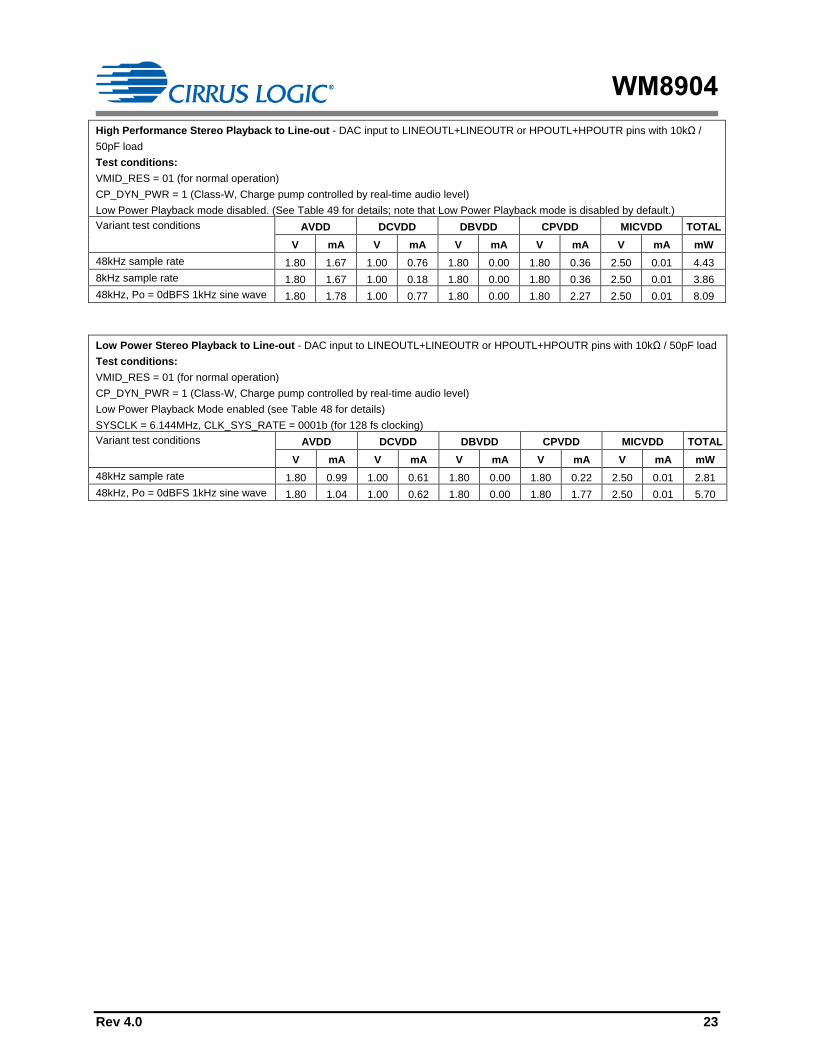
High Performance Stereo Playback to Line-out - DAC input to LINEOUTL+LINEOUTR or HPOUTL+HPOUTR pins with 10kΩ /
50pF load
Test conditions:
VMID_RES = 01 (for normal operation)
CP_DYN_PWR = 1 (Class-W, Charge pump controlled by real-time audio level)
Low Power Playback mode disabled. (See Table 49 for details; note that Low Power Playback mode is disabled by default.)
Variant test conditions AVDD DCVDD DBVDD CPVDD MICVDD TOTAL
V mA V mA V mA V mA V mA mW
48kHz sample rate 1.80 1.67 1.00 0.76 1.80 0.00 1.80 0.36 2.50 0.01 4.43
8kHz sample rate 1.80 1.67 1.00 0.18 1.80 0.00 1.80 0.36 2.50 0.01 3.86
48kHz, Po = 0dBFS 1kHz sine wave 1.80 1.78 1.00 0.77 1.80 0.00 1.80 2.27 2.50 0.01 8.09
Low Power Stereo Playback to Line-out - DAC input to LINEOUTL+LINEOUTR or HPOUTL+HPOUTR pins with 10kΩ / 50pF load
Test conditions:
VMID_RES = 01 (for normal operation)
CP_DYN_PWR = 1 (Class-W, Charge pump controlled by real-time audio level)
Low Power Playback Mode enabled (see Table 48 for details)
SYSCLK = 6.144MHz, CLK_SYS_RATE = 0001b (for 128 fs clocking)
Variant test conditions AVDD DCVDD DBVDD CPVDD MICVDD TOTAL
V mA V mA V mA V mA V mA mW
48kHz sample rate 1.80 0.99 1.00 0.61 1.80 0.00 1.80 0.22 2.50 0.01 2.81
48kHz, Po = 0dBFS 1kHz sine wave 1.80 1.04 1.00 0.62 1.80 0.00 1.80 1.77 2.50 0.01 5.70

WM8904
24 Rev 4.0
Stereo analogue bypass to headphones - IN1L/R, IN2L/R or IN3L/R pins to HPOUTL+HPOUTR pins with 30Ω load.
Test conditions:
LIN_VOL = RIN_VOL = 00101 = +0.0 dB
MCLK = 11.2896MHz
Digital audio interface disabled
Note that the Analogue bypass configuration does not benefit from the Class W dynamic control.
Variant test conditions AVDD DCVDD DBVDD CPVDD MICVDD TOTAL
V mA V mA V mA V mA V mA mW
Quiescent
HPOUTVOL = 000000 (-57dB) 1.8 1.24 1 0.11 1.8 0.00 1.8 0.26 2.5 0.01 2.82
Po = 0.1mW/channel 1kHz sine wave
HPOUTVOL = 100000 (-25dB) 1.8 1.29 1 0.11 1.8 0.00 1.8 2.05 2.5 0.01 6.13
Po = 1mW/channel 1kHz sine wave
HPOUTVOL = 101010 (-15dB) 1.8 1.30 1 0.11 1.8 0.00 1.8 5.86 2.5 0.01 13.02
Stereo analogue bypass to Line-out - IN1L/R, IN2L/R or IN3L/R pins to LINEOUTL+LINEOUTR pins with 30Ω load.
Test conditions:
LIN_VOL = RIN_VOL = 00101 = +0.0 dB
MCLK = 11.2896MHz
Digital audio interface disabled
Note that the Analogue bypass configuration does not benefit from the Class W dynamic control.
Variant test conditions AVDD DCVDD DBVDD CPVDD MICVDD TOTAL
V mA V mA V mA V mA V mA mW
Quiescent
LINEOUTVOL = 000000 (-57dB) 1.8 1.04 1.0 0.15 1.8 0.00 1.8 0.21 1.8 0.01 2.41
Quiescent
LINEOUTVOL = 101011 (-14dB) 1.8 1.04 1.0 0.15 1.8 0.00 1.8 0.63 1.8 0.01 3.18
Quiescent
LINEOUTVOL = 111001 (0dB) 1.8 1.04 1.0 0.15 1.8 0.00 1.8 1.25 1.8 0.01 4.28
Off
Note: DC servo calibration is retained in this state as long as DCVDD is supplied. This allows fast, pop suppressed start-up from the off state.
Variant test conditions AVDD DCVDD DBVDD CPVDD MICVDD TOTAL
V mA V mA V mA V mA V mA mW
Off (default settings)
No Clocks applied
1.8 0.01 1 0.00 1.8 0.00 1.8 0.01 2.5 0.01 0.04
Off (default settings)
DACDAT, MCLK, BCLK, and LRCLK
applied
1.8 0.01 1 0.02 1.8 0.00 1.8 0.01 2.5 0.01 0.06

WM8904
Rev 4.0 25
SIGNAL TIMING REQUIREMENTS
COMMON TEST CONDITIONS
Unless otherwise stated, the following test conditions apply throughout the following sections:
Ambient temperature = +25°C
DCVDD = 1.0V
DBVDD = AVDD = CPVDD = 1.8V
DGND = AGND = CPGND = 0V
Additional, specific test conditions are given within the relevant sections below.
MASTER CLOCK
MCLK
tMCLKL tMCLKH
tMCLKY
Figure 1 Master Clock Timing
Master Clock Timing
PARAMETER SYMBOL TEST CONDITIONS MIN TYP MAX UNIT
MCLK cycle time TMCLKY MCLK_DIV=1 40 ns
MCLK_DIV=0 80 ns
MCLK duty cycle TMCLKDS 60:40 40:60

WM8904
26 Rev 4.0
AUDIO INTERFACE TIMING
MASTER MODE
BCLK (Output)
ADCDAT
LRCLK (Output)
tDL
DACDAT
tDDA
tDHT
tDST
Figure 2 Audio Interface Timing – Master Mode
Test Conditions
DCVDD = 1.0V, AVDD = DBVDD = CPVDD = 1.8V, DGND=AGND=CPGND =0V, TA = +25oC, Master Mode, fs=48kHz,
MCLK=256fs, 24-bit data, unless otherwise stated.
PARAMETER SYMBOL MIN TYP MAX UNIT
Audio Interface Timing - Master Mode
LRCLK propagation delay from BCLK falling edge tDL 20 ns
ADCDAT propagation delay from BCLK falling edge tDDA 20 ns
DACDAT setup time to BCLK rising edge tDST 20 ns
DACDAT hold time from BCLK rising edge tDHT 10 ns

WM8904
Rev 4.0 27
SLAVE MODE
BCLK (input)
LRCLK (input)
ADCDAT (output)
DACDAT (input)
tDS
tDD
tDH
tLRH tLRSU
tBCH tBCL
tBCY
Figure 3 Audio Interface Timing – Slave Mode
Test Conditions
DCVDD = 1.0V, AVDD = DBVDD = CPVDD = 1.8V, DGND=AGND=CPGND =0V, TA = +25oC, Slave Mode, fs=48kHz,
MCLK=256fs, 24-bit data, unless otherwise stated.
PARAMETER SYMBOL MIN TYP MAX UNIT
Audio Interface Timing - Slave Mode
BCLK cycle time tBCY 50 ns
BCLK pulse width high tBCH 20 ns
BCLK pulse width low tBCL 20 ns
LRCLK set-up time to BCLK rising edge tLRSU 20 ns
LRCLK hold time from BCLK rising edge tLRH 10 ns
DACDAT hold time from BCLK rising edge tDH 10 ns
ADCDAT propagation delay from BCLK falling edge tDD 20 ns
DACDAT set-up time to BCLK rising edge tDS 20 ns
Note: BCLK period must always be greater than or equal to MCLK period.

WM8904
28 Rev 4.0
TDM MODE
In TDM mode, it is important that two ADC devices do not attempt to drive the ADCDAT pin
simultaneously. The timing of the WM8904 ADCDAT tri-stating at the start and end of the data
transmission is described below.
BCLK
ADCDAT ADCDAT undriven (tri-state) ADCDAT valid (CODEC output) ADCDAT valid ADCDAT undriven (tri-state)
ADCDAT set-up time ADCDAT release time
Figure 4 Audio Interface Timing - TDM Mode
Test Conditions
AVDD = CPVDD = 1.8V , DGND=AGND=CPGND= =0V, TA = +25oC, Master Mode, fs=48kHz, MCLK=256fs, 24-bit data, unless
otherwise stated.
PARAMETER CONDITIONS MIN TYP MAX UNIT
Audio Data Timing Information
ADCDAT setup time from BCLK falling edge DCVDD =2.0V
DBVDD =
3.6V
5 ns
DCVDD =
1.08V DBVDD
= 1.62V
15 ns
ADCDAT release time from BCLK falling edge DCVDD =
2.0V DBVDD
= 3.6V
5 ns
DCVDD =
1.08V DBVDD
= 1.62V
15 ns

WM8904
Rev 4.0 29
CONTROL INTERFACE TIMING
SCLK
(input)
SDA
t4 t3
START
t8
STOP
t5
t2 t1
t9
t7
t6
Figure 5 Control Interface Timing
Test Conditions
DCVDD = 1.0V, AVDD = DBVDD = CPVDD = 1.8V, DGND=AGND=CPGND =0V, TA=+25oC, Slave Mode, fs=48kHz, MCLK =
256fs, 24-bit data, unless otherwise stated.
PARAMETER SYMBOL MIN TYP MAX UNIT
SCLK Frequency 400 kHz
SCLK Low Pulse-Width t1 1300 ns
SCLK High Pulse-Width t2 600 ns
Hold Time (Start Condition) t3 600 ns
Setup Time (Start Condition) t4 600 ns
Data Setup Time t5 100 ns
SDA, SCLK Rise Time t6 300 ns
SDA, SCLK Fall Time t7 300 ns
Setup Time (Stop Condition) t8 600 ns
Data Hold Time t9 900 ns
Pulse width of spikes that will be suppressed tps 0 5 ns

WM8904
30 Rev 4.0
DIGITAL FILTER CHARACTERISTICS
PARAMETER TEST CONDITIONS MIN TYP MAX UNIT
ADC Filter
Passband +/- 0.05dB 0 0.454 fs
-6dB 0.5 fs
Passband Ripple +/- 0.05 dB
Stopband 0.546s
Stopband Attenuation f > 0.546 fs -60 dB
DAC Normal Filter
Passband +/- 0.05dB 0 0.454 fs
-6dB 0.5 fs
Passband Ripple 0.454 fs +/- 0.03 dB
Stopband 0.546 fs
Stopband Attenuation F > 0.546 fs -50 dB
DAC Sloping Stopband Filter
Passband +/- 0.03dB 0 0.25 fs
+/- 1dB 0.25 fs 0.454 fs
-6dB 0.5 fs
Passband Ripple 0.25 fs +/- 0.03 dB
Stopband 1 0.546 fs 0.7 fs
Stopband 1 Attenuation f > 0.546 fs -60 dB
Stopband 2 0.7 fs 1.4 fs
Stopband 2 Attenuation f > 0.7 fs -85 dB
Stopband 3 1.4 fs
Stopband 3 Attenuation F > 1.4 fs -55 dB
DAC FILTERS ADC FILTERS
Mode Group Delay Mode Group Delay
Normal 16.5 / fs Normal 16.5 / fs
Sloping Stopband 18 / fs
TERMINOLOGY
1. Stop Band Attenuation (dB) – the degree to which the frequency spectrum is attenuated (outside audio band)
2. Pass-band Ripple – any variation of the frequency response in the pass-band region

WM8904
Rev 4.0 31
ADC FILTER RESPONSES
Figure 6 ADC Digital Filter Frequency Response Figure 7 ADC Digital Filter Ripple
ADC HIGH PASS FILTER RESPONSES
hpf_response.res MAGNITUDE(dB) hpf_response2.res MAGNITUDE(dB)
hpf_response2.res#1 MAGNITUDE(dB)
2 5.0248 12.624 31.716 79.683 200.19 502.96 1.2636k 3.1747k 7.9761k 20.039k
-83.352
-75.017
-66.682
-58.347
-50.012
-41.677
-33.342
-25.007
-16.672
-8.3373
-2.3338m
Figure 8 ADC Digital High Pass Filter Frequency Response
(48kHz, Hi-Fi Mode, ADC_HPF_CUT[1:0]=00)
Figure 9 ADC Digital High Pass Filter Ripple (48kHz,
Voice Mode, ADC_HPF_CUT=01, 10 and 11)

WM8904
32 Rev 4.0
DAC FILTER RESPONSES
MAGNITUDE(dB)
-0.005
0
0.005
0.01
0.015
0.02
0.025
0.03
0.035
0.04
0 0.05 0.1 0.15 0.2 0.25 0.3 0.35 0.4 0.45 0.5
Frequency (fs)
Figure 10 DAC Digital Filter Frequency Response; (Normal
Mode); Sample Rate > 24kHz
Figure 11 DAC Digital Filter Ripple (Normal Mode)
MAGNITUDE(dB)
-0.5
-0.45
-0.4
-0.35
-0.3
-0.25
-0.2
-0.15
-0.1
-0.05
0
0.05
0 0.05 0.1 0.15 0.2 0.25 0.3 0.35 0.4 0.45 0.5
Frequency (fs)
Figure 12 DAC Digital Filter Frequency Response; (Sloping
Stopband Mode); Sample Rate <= 24kHz
Figure 13 DAC Digital Filter Ripple (Sloping Stopband
Mode)

WM8904
Rev 4.0 33
DE-EMPHASIS FILTER RESPONSES
MAGNITUDE(dB)
-10
-9
-8
-7
-6
-5
-4
-3
-2
-1
0
0 5000 10000 15000 20000
Frequency (Hz)
MAGNITUDE(dB)
-0.15
-0.1
-0.05
0
0.05
0.1
0.15
0.2
0.25
0.3
0 2000 4000 6000 8000 10000 12000 14000 16000 18000
Frequency (Hz)
Figure 14 De-Emphasis Digital Filter Response (32kHz) Figure 15 De-Emphasis Error (32kHz)
MAGNITUDE(dB)
-10
-9
-8
-7
-6
-5
-4
-3
-2
-1
0
0 5000 10000 15000 20000 25000
Frequency (Hz)
MAGNITUDE(dB)
-0.1
-0.05
0
0.05
0.1
0.15
0.2
0 5000 10000 15000 20000 25000
Frequency (Hz)
Figure 16 De-Emphasis Digital Filter Response (44.1kHz) Figure 17 De-Emphasis Error (44.1kHz)
MAGNITUDE(dB)
-12
-10
-8
-6
-4
-2
0
0 5000 10000 15000 20000 25000 30000
Frequency (Hz)
MAGNITUDE(dB)
-0.15
-0.1
-0.05
0
0.05
0.1
0.15
0 5000 10000 15000 20000 25000 30000
Frequency (Hz)
Figure 18 De-Emphasis Digital Filter Response (48kHz) Figure 19 De-Emphasis Error (48kHz)

WM8904
34 Rev 4.0
DEVICE DESCRIPTION
INTRODUCTION
The WM8904 is a high performance ultra-low power stereo CODEC optimised for portable audio
applications. Flexible analogue interfaces and powerful digital signal processing (DSP) make it ideal
for small portable devices.
The WM8904 supports up to 6 analogue audio inputs. One pair of single-ended or differential
microphone/line inputs is selected as the ADC input source. An integrated bias reference is provided
to power standard electret microphones.
A two-channel digital microphone interface is also supported, with direct input to the DSP core
bypassing the ADCs.
One pair of ground-reference Class-W headphone outputs is provided; these are powered from an
integrated Charge Pump, enabling high quality, power efficient headphone playback without any
requirement for DC blocking capacitors. A DC Servo circuit is available for DC offset correction,
thereby suppressing pops and reducing power consumption. Two line outputs are provided; these are
also capable of driving ear speakers and stereo headsets. Ground loop feedback is available on the
headphone outputs and the line outputs, providing rejection of noise on the ground connections. All
outputs use SilentSwitch technology for pop and click suppression.
The stereo ADCs and DACs are of hi-fi quality, using a 24-bit low-order oversampling architecture to
deliver optimum performance. A flexible clocking arrangement supports mixed ADC and DAC sample
rates, whilst an integrated ultra-low power FLL provides additional flexibility. A high pass filter is
available in the ADC path for removing DC offsets and suppressing low frequency noise such as
mechanical vibration and wind noise. A digital mixing path from the ADC to the DAC provides a
sidetone of enhanced quality during voice calls. DAC soft mute and un-mute is available for pop-free
music playback.
The integrated Dynamic Range Controller (DRC) and ReTuneTM Mobile 5-band parametric equaliser
(EQ) provide further processing capability of the digital audio paths. The DRC provides compression
and signal level control to improve the handling of unpredictable signal levels. ‘Anti-clip’ and ‘quick
release’ algorithms improve intelligibility in the presence of transients and impulsive noises. The EQ
provides the capability to tailor the audio path according to the frequency characteristics of an
earpiece or loudspeaker, and/or according to user preferences.
The WM8904 has a highly flexible digital audio interface, supporting a number of protocols, including
I2S, DSP, MSB-first left/right justified, and can operate in master or slave modes. PCM operation is
supported in the DSP mode. A-law and -law companding are also supported. Time division
multiplexing (TDM) is available to allow multiple devices to stream data simultaneously on the same
bus, saving space and power.
The system clock SYSCLK provides clocking for the ADCs, DACs, DSP core, digital audio interface
and other circuits. SYSCLK can be derived directly from the MCLK pin or via an integrated FLL,
providing flexibility to support a wide range of clocking schemes. Typical portable system MCLK
frequencies, and sample rates from 8kHz to 48kHz are all supported. The clocking circuits are
configured automatically from the sample rate (fs) and from the SYSCLK / fs ratio.
The integrated FLL can be used to generate SYSCLK from a wide variety of different reference
sources and frequencies. The FLL can accept a wide range of reference frequencies, which may be
high frequency (e.g. 13MHz) or low frequency (eg. 32.768kHz). The FLL is tolerant of jitter and may
be used to generate a stable SYSCLK from a less stable input signal. The integrated FLL can be used
as a free-running oscillator, enabling autonomous clocking of the Charge Pump and DC Servo if
required.
The WM8904 uses a standard 2-wire control interface, providing full software control of all features,
together with device register readback. An integrated Control Write Sequencer enables automatic
scheduling of control sequences; commonly-used signal configurations may be selected using ready-
programmed sequences, including time-optimised control of the WM8904 pop suppression features. It
is an ideal partner for a wide range of industry standard microprocessors, controllers and DSPs.
Unused circuitry can be disabled under software control, in order to save power; low leakage currents
enable extended standby/off time in portable battery-powered applications.
Up to 4 GPIO pins may be configured for miscellaneous input/output functions such as
button/accessory detect inputs, or for clock, system status, or programmable logic level output for

WM8904
Rev 4.0 35
control of additional external circuitry. Interrupt logic, status readback and de-bouncing options are
supported within this functionality.
ANALOGUE INPUT SIGNAL PATH
The WM8904 has six analogue input pins, which may be used to support connections to multiple
microphone or line input sources. The input multiplexer on the Left and Right channels can be used to
select different configurations for each of the input sources. The analogue input paths can support line
and microphone inputs, in single-ended and differential modes. The input stage can also provide
common mode noise rejection in some configurations.
Two of the six analogue input pins have dual functionality and can be used as digital microphone
inputs. (See the “Digital Microphone Interface” section for details.)
The Left and Right analogue input channels are routed to the Analogue to Digital converters (ADCs).
There is also a bypass path for each channel, enabling the signal to be routed directly to the output
multiplexers and PGAs.
The WM8904 input signal paths and control registers are illustrated in Figure 20.
Single-Ended (inverting) Mode: Gain -1.57dB to +28.5dB, non-linear steps
Differential Line Mode: Gain -1.57dB to +28.5dB, non-linear steps
Differential Microphone Mode: Gain +12dB to +30dB, 3dB steps
MUX
IN1L/DMICDAT1
IN3L
IN2L -
+
L_MODE
L_IP_SEL_N
L_IP_SEL_P
INL_ENA
INL_CM_ENA
LIN_MUTE
LIN_VOL
AG
ND
AV
DD
VMID
BYPASSL
MUX
IN1R/DMICDAT2
IN3R
IN2R -
+
R_MODE
R_IP_SEL_N
R_IP_SEL_P
INR_ENA
INR_CM_ENA
RIN_MUTE
RIN_VOL
VMID
BYPASSR
ADC L
ADC R
Single-Ended (inverting) Mode: Gain -1.57dB to +28.5dB, non-linear steps
Differential Line Mode: Gain -1.57dB to +28.5dB, non-linear steps
Differential Microphone Mode: Gain +12dB to +30dB, 3dB steps
Figure 20 Block Diagram for Input Signal Path

WM8904
36 Rev 4.0
INPUT PGA ENABLE
The input PGAs (Programmable Gain Amplifiers) and Multiplexers are enabled using register bits
INL_ENA and INR_ENA, as shown in Table 1.
REGISTER
ADDRESS
BIT LABEL DEFAULT DESCRIPTION
R12 (0Ch)
Power
Management
0
1 INL_ENA 0 Left Input PGA Enable
0 = disabled
1 = enabled
0 INR_ENA 0 Right Input PGA Enable
0 = disabled
1 = enabled
Table 1 Input PGA Enable
To enable the input PGAs, the reference voltage VMID and the bias current must also be enabled.
See Reference Voltages and Master Bias for details of the associated controls VMID_RES and
BIAS_ENA.
INPUT PGA CONFIGURATION
The analogue input channels can each be configured in three different modes, which are as follows:
Single-Ended Mode (Inverting)
Differential Line Mode
Differential Mic Mode
The mode is selected by the L_MODE and R_MODE fields for the Left and Right channels
respectively. The input pins are selected using the L_IP_SEL_N and L_IP_SEL_P fields for the Left
channel and the R_IP_SEL_N and R_IP_SEL_P for the Right channel. In Single-Ended mode,
L_IP_SEL_N alone determines the Left Input pin, and the R_IP_SEL_N determines the Right Input
pin.
The three modes are illustrated in Figure 21, Figure 22 and Figure 23. It should be noted that the
available gain and input impedance varies between configurations (see also “Electrical
Characteristics”). The input impedance is constant with PGA gain setting.
The Input PGA modes are selected and configured using the register fields described in Table 2
below.

WM8904
Rev 4.0 37
REGISTER
ADDRESS
BIT LABEL DEFAULT DESCRIPTION
R46 (2Eh)
Analogue
Left Input 1
5:4 L_IP_SEL_N [1:0] 00 In Single-Ended or Differential Line
Modes, this field selects the input pin
for the inverting side of the left input
path.
In Differential Mic Mode, this field
selects the input pin for the non-
inverting side of the left input path.
00 = IN1L
01 = IN2L
1X = IN3L
3:2 L_IP_SEL_P [1:0] 01 In Single-Ended or Differential Line
Modes, this field selects the input pin
for the non-inverting side of the left
input path.
In Differential Mic Mode, this field
selects the input pin for the inverting
side of the left input path.
00 = IN1L
01 = IN2L
1X = IN3L
1:0 L_MODE [1:0] 00 Sets the mode for the left analogue
input:
00 = Single-Ended
01 = Differential Line
10 = Differential MIC
11 = Reserved
R47 (2Fh)
Analogue
Right Input
1
5:4 R_IP_SEL_N [1:0] 00 In Single-Ended or Differential Line
Modes, this field selects the input pin
for the inverting side of the right input
path.
In Differential Mic Mode, this field
selects the input pin for the non-
inverting side of the right input path.
00 = IN1R
01 = IN2R
1X = IN3R
3:2 R_IP_SEL_P [1:0] 01 In Single-Ended or Differential Line
Modes, this field selects the input pin
for the non-inverting side of the right
input path.
In Differential Mic Mode, this field
selects the input pin for the inverting
side of the right input path.
00 = IN1R
01 = IN2R
1X = IN3R
1:0 R_MODE [1:0] 00 Sets the mode for the right analogue
input:
00 = Single-Ended
01 = Differential Line
10 = Differential MIC
11 = Reserved
Table 2 Input PGA Mode Selection

WM8904
38 Rev 4.0
SINGLE-ENDED INPUT
The Single-Ended PGA configuration is illustrated in Figure 21 for the Left channel. The available gain
in this mode is from -1.57dB to +28.5dB in non-linear steps. The input to the ADC is phase inverted
with respect to the selected input pin. Different input pins can be selected in the same mode by
altering the L_IP_SEL_N field.
The equivalent configuration is also available on the Right channel; this can be selected
independently of the Left channel mode.
BYPASSL
IN1L/DMICDAT1
IN3L
IN2L -
+
L_IP_SEL_N
-1.57dB to +28.5dB,
non-linear steps
INL_ENA
LIN_MUTE
LIN_VOL
ADC L
VMID
M
U
X
Single-Ended (inverting) Mode (L_MODE = 00)
Figure 21 Single Ended Mode
DIFFERENTIAL LINE INPUT
The Differential Line PGA configuration is illustrated in Figure 22 for the Left channel. The available
gain in this mode is from -1.57dB to +28.5dB in non-linear steps. The input to the ADC is in phase with
the input pin selected by L_IP_SEL_P. The input to the ADC is phase inverted with respect to the
input pin selected by L_IP_SEL_N.
As an option, common mode noise rejection can be provided in this PGA configuration, as illustrated
in Figure 22. This is enabled using the register bits defined in Table 5.
The equivalent configuration is also available on the Right channel; this can be selected
independently of the Left channel mode.
BYPASSL
IN1L/DMICDAT1
IN3L
IN2L -
+
L_IP_SEL_NINL_ENA
LIN_MUTE
LIN_VOL
ADC L
M
U
X
L_IP_SEL_P
M
U
X
Differential Line Mode (L_MODE = 01)
-1.57dB to +28.5dB,
non-linear steps
INL_CM_ENA
+
-
Figure 22 Differential Line Mode

WM8904
Rev 4.0 39
DIFFERENTIAL MICROPHONE INPUT
The Differential Mic PGA configuration is illustrated in Figure 23 for the Left channel. The available
gain in this mode is from +12dB to +30dB in 3dB linear steps. The input to the ADC is in phase with
the input pin selected by L_IP_SEL_N. The input to the ADC is phase inverted with respect to the
input pin selected by L_IP_SEL_P.
Note that the inverting input pin is selected using L_IP_SEL_P and the non-inverting input pin is
selected using L_IP_SEL_N. This is not the same as for the Differential Line mode.
The equivalent configuration is also available on the Right channel; this can be selected
independently of the Left channel mode.
BYPASSL
IN1L/DMICDAT1
IN3L
IN2L
L_IP_SEL_N
INL_ENA
LIN_MUTE
LIN_VOL ADC L
M
U
X
L_IP_SEL_P
M
U
X
Differential Microphone Mode (L_MODE = 10)
+12dB to +30dB,
3dB steps
INL_ENA
LIN_MUTE
LIN_VOL
+12dB to +30dB,
3dB steps
+
-
Figure 23 Differential Microphone Mode
INPUT PGA GAIN CONTROL
The volume control gain for the Left and Right channels be independently controlled using the
LIN_VOL and RIN_VOL register fields as described in Table 3. The available gain range varies
according to the selected PGA Mode as detailed in Table 4. Note that the value ‘00000’ must not be
used in Differential Mic Mode, as the PGA will not function correctly under this setting. In single-ended
mode (L_MODE / R_MODE = 00b), the conversion from single-ended to differential within the
WM8904 adds a further 6dB of gain to the signal path.
Each input channel can be independently muted using LINMUTE and RINMUTE.
It is recommended to not adjust the gain dynamically whilst the signal path is enabled; the signal
should be muted at the input or output stage prior to adjusting the volume control.
REGISTER
ADDRESS
BIT LABEL DEFAULT DESCRIPTION
R44 (2Ch)
Analogue Left
Input 0
7 LINMUTE 1 Left Input PGA Mute
0 = not muted
1 = muted
4:0 LIN_VOL [4:0] 00101 Left Input PGA Volume
(See Table 4 for volume range)
R45 (2Dh)
Analogue
Right Input 0
7 RINMUTE 1 Right Input PGA Mute
0 = not muted
1 = muted
4:0 RIN_VOL [4:0] 00101 Right Input PGA Volume
(See Table 4 for volume range)
Table 3 Input PGA Volume Control

WM8904
40 Rev 4.0
LIN_VOL [4:0],
RIN_VOL [4:0]
GAIN –
SINGLE-ENDED MODE /
DIFFERENTIAL LINE MODE
GAIN –
DIFFERENTIAL MIC MODE
00000 -1.5 dB Not valid
00001 -1.3 dB +12 dB
00010 -1.0 dB +15 dB
00011 -0.7 dB +18 dB
00100 -0.3 dB +21 dB
00101 0.0 dB +24 dB
00110 +0.3 dB +27 dB
00111 +0.7 dB +30 dB
01000 +1.0 dB +30 dB
01001 +1.4 dB +30 dB
01010 +1.8 dB +30 dB
01011 +2.3 dB +30 dB
01100 +2.7 dB +30 dB
01101 +3.2 dB +30 dB
01110 +3.7 dB +30 dB
01111 +4.2 dB +30 dB
10000 +4.8 dB +30 dB
10001 +5.4 dB +30 dB
10010 +6.0 dB +30 dB
10011 +6.7 dB +30 dB
10100 +7.5 dB +30 dB
10101 +8.3 dB +30 dB
10110 +9.2 dB +30 dB
10111 +10.2 dB +30 dB
11000 +11.4 dB +30 dB
11001 +12.7 dB +30 dB
11010 +14.3 dB +30 dB
11011 +16.2 dB +30 dB
11100 +19.2 dB +30 dB
11101 +22.3 dB +30 dB
11110 +25.2 dB +30 dB
11111 +28.3 dB +30 dB
Table 4 Input PGA Volume Range

WM8904
Rev 4.0 41
INPUT PGA COMMON MODE AMPLIFIER
In Differential Line Mode only, a Common Mode amplifier can be enabled as part of the input PGA
circuit. This feature provides approximately 20dB reduction in common mode noise on the differential
input, which can reduce problematic interference. Since the ADC has differential signal inputs, it has
an inherent immunity to common mode noise (see “Electrical Characteristics”) However, the presence
of Common Mode noise can limit the usable signal range of the ADC path; enabling the Common
Mode amplifier can solve this issue.
It should be noted that the Common Mode amplifier consumes additional power and can also add its
own noise to the input signal. For these reasons, it is recommended that the Common Mode Amplifier
is only enabled if there is a known source of Common Mode interference.
The Common Mode amplifier is controlled by the INL_CM_ENA and INR_CM_ENA fields as
described in Table 5. Although the Common Mode amplifier may be enabled regardless of the input
PGA mode, its function is only effective in the Differential Line Mode configuration.
REGISTER
ADDRESS
BIT LABEL DEFAULT DESCRIPTION
R46 (2Eh)
Analogue Left
Input 1
6 INL_CM_ENA 1 Left Input PGA Common Mode
Rejection enable
0 = Disabled
1 = Enabled
(only available for L_MODE=01 –
Differential Line)
R47 (2Fh)
Analogue
Right Input 1
6 INR_CM_ENA 1 Right Input PGA Common Mode
Rejection enable
0 = Disabled
1 = Enabled
(only available for R_MODE=01 –
Differential Line)
Table 5 Common Mode Amplifier Enable

WM8904
42 Rev 4.0
ELECTRET CONDENSER MICROPHONE INTERFACE
Electret Condenser microphones may be connected as single-ended or differential inputs to the Input
PGAs described in the “Analogue Input Signal Path” section. The WM8904 provides a low-noise
reference voltage (MICBIAS) suitable for biasing electret condenser microphones.
MICBIAS CONTROL
The MICBIAS reference is provided on the MICBIAS pin. This reference voltage is enabled by setting
the MICBIAS_ENA register bit.
The MICBIAS output voltage is selected using the MICBIAS_SEL register. This register selects the
output voltage as a ratio of AVDD; the actual output voltage scales with AVDD.
The MICBIAS output is powered from the MICVDD supply pin, and uses VMID (ie. AVDD/2) as a
reference, as illustrated in Figure 24. In all cases, MICVDD must be at least 200mV greater than the
required MICBIAS output voltage.
Under the default setting of MICBIAS_SEL, the MICVDD supply may be connected directly to AVDD.
For other settings of MICBIAS_SEL, (ie. for higher MICBIAS voltages), the MICVDD supply must be
greater than AVDD.
The MICBIAS generator is illustrated in in Figure 24. The associated control registers are defined in
Table 6.
VMIDC
WM8904
MICBIAS
MICVDD
AGND
MICBIAS_ENA
MICBIAS_SEL[2:0]
Figure 24 MICBIAS Generator
REGISTER
ADDRESS
BIT LABEL DEFAULT DESCRIPTION
R6 (06h)
Mic Bias
Control 0
0 MICBIAS_ENA 0 MICBIAS Enable
0 = disabled
1 = enabled
R7 (07h)
Mic Bias
Control 1
2:0 MICBIAS_SEL [2:0] 000 Selects MICBIAS voltage
000 = 9/10 x AVDD (1.6V)
001 = 10/9 x AVDD (2.0V)
010 = 7/6 x AVDD (2.1V)
011 = 4/3 x AVDD (2.4V)
100 to 111 = 3/2 x AVDD (2.7V)
Note that the voltage scales with
AVDD. The value quoted in
brackets is correct for AVDD=1.8V.
Table 6 MICBIAS Control

WM8904
Rev 4.0 43
MICBIAS CURRENT DETECT
A MICBIAS Current Detect function is provided for external accessory detection. This is provided in
order to detect the insertion/removal of a microphone or the pressing/releasing of the microphone
‘hook’ switch; these events will cause a significant change in MICBIAS current flow, which can be
detected and used to generate a signal to the host processor.
The MICBIAS current detect function is enabled by setting the MICDET_ENA register bit. When this
function is enabled, two current thresholds can be defined, using the MICDET_THR and
MICSHORT_THR registers. When a change in MICBIAS current which crosses either threshold is
detected, then an interrupt event can be generated. In a typical application, accessory insertion would
be detected when the MICBIAS current exceeds MICDET_THR, and microphone hookswitch
operation would be detected when the MICBIAS current exceeds MICSHORT_THR.
The current detect threshold functions are both inputs to the Interrupt control circuit and can be used
to trigger an Interrupt event when either threshold is crossed. Both events can also be indicated as an
output on a GPIO pin - see “General Purpose Input/Output (GPIO)”.
The current detect thresholds are enabled and controlled using the registers described in Table 7.
Performance parameters for this circuit block can be found in the “Electrical Characteristics” section.
Hysteresis and filtering is also provided in the both current detect circuits to improve reliability in
conditions where AC current spikes are present due to ambient noise conditions. These features are
described in the following section. Further guidance on the usage of the MICBIAS current monitoring
features is also described in the following pages.
REGISTER
ADDRESS
BIT LABEL DEFAULT DESCRIPTION
R6 (06h)
Mic Bias
Control 0
6:4 MICDET_THR [2:0] 000 MICBIAS Current Detect Threshold
(AVDD = 1.8V)
000 = 0.070mA
001 = 0.260mA
010 = 0.450mA
011 = 0.640mA
100 = 0.830mA
101 = 1.020mA
110 = 1.210mA
111 = 1.400mA
Note that the value scales with
AVDD. The value quoted is correct
for AVDD=1.8V.
3:2 MICSHORT_THR
[1:0]
00 MICBIAS Short Circuit Threshold
(AVDD = 1.8V)
00 = 0.520mA
01 = 0.880mA
10 = 1.240mA
11 = 1.600mA
Note that the value scales with
AVDD. The value quoted is correct
for AVDD=1.8V.
1 MICDET_ENA 0 MICBIAS Current and Short Circuit
Detect Enable
0 = disabled
1 = enabled
Table 7 MICBIAS Current Detect
MICBIAS CURRENT DETECT FILTERING
The function of the filtering is to ensure that AC current spikes caused by ambient noise conditions
near the microphone do not lead to incorrect signalling of the microphone insertion/removal status or
the microphone hookswitch status.

WM8904
44 Rev 4.0
Hysteresis on the current thresholds is provided; this means that a different current threshold is used
to detect microphone insertion and microphone removal. Similarly, a different current threshold is
used to detect hookswitch press and hookswtich release.
Digital filtering of the hookswitch status ensures that the MICBIAS Short Circuit detection event is only
signalled if the MICSHORT_THR threshold condition has been met for 10 consecutive measurements.
In a typical application, microphone insertion would be detected when the MICBIAS current exceeds
the Current Detect threshold set by MICDET_THR.
When the MIC_DET_EINT_POL interrupt polarity bit is set to 0, then microphone insertion detection
will cause the MIC_DET_EINT interrupt status register to be set.
For detection of microphone removal, the MIC_DET_EINT_POL bit should be set to 1. When the
MIC_DET_EINT_POL interrupt polarity bit is set to 1, then microphone removal detection will cause
the MIC_DET_EINT interrupt status register to be set.
The detection of these events is bandwidth limited for best noise rejection, and is subject to detection
delay time tDET, as specified in the “Electrical Characteristics”. Provided that the MICDET_THR field
has been set appropriately, each insertion or removal event is guaranteed to be detected within the
delay time tDET.
It is likely that the microphone socket contacts will have mechanical “bounce” when a microphone is
inserted or removed, and hence the resultant control signal will not be a clean logic level transition.
Since tDET has a range of values, it is possible that the interrupt will be generated before the
mechanical “bounce” has ceased. Hence after a mic insertion or removal has been detected, a time
delay should be applied before re-configuring the MIC_DET_EINT_POL bit. The maximum possible
mechanical bounce times for mic insertion and removal must be understood by the software
programmer.
Utilising a GPIO pin to monitor the steady state of the microphone detection function does not change
the timing of the detection mechanism, so there will also be a delay tDET before the signal changes
state. It may be desirable to implement de-bounce in the host processor when monitoring the state of
the GPIO signal.
Microphone hook switch operation is detected when the MICBIAS current exceeds the Short Circuit
Detect threshold set by MICSHORT_THR. Using the digital filtering, the hook switch detection event is
only signalled if the MICSHORT_THR threshold condition has been met for 10 consecutive
measurements.
When the MIC_SHRT_EINT_POL interrupt polarity bit is set to 0, then hook switch operation will
cause the MIC_SHRT_EINT interrupt status register to be set.
For detection of microphone removal, the MIC_SHRT_EINT_POL bit should be set to 1. When the
MIC_SHRT_EINT_POL interrupt polarity bit is set to 1, then hook switch release will cause the
MIC_SHRT_EINT interrupt status register to be set.
The hook switch detection measurement frequency and the detection delay time tSHORT are detailed in
the “Electrical Characteristics” section.
The WM8904 Interrupt function is described in the “Interrupts” section. Example control sequences for
configuring the Interrupts functions for MICBIAS current detection events are described in the
“Applications Information” section.
A clock is required for the digital filtering function, and the DC Servo must also be running. This
requires:
MCLK is present or the FLL is selected as the SYSCLK source in free-running mode
CLK_SYS_ENA = 1
DCS_ENA_CHAN_n is enabled (where n = 0, 1, 2 or 3)

WM8904
Rev 4.0 45
Any MICBIAS Current Detect event (accessory insertion/removal or hookswitch press/release) which
happens while one or more of the clocking criteria is not satisfied (for example during a low power
mode where the CPU has disabled MCLK) will still be detected, but only after the clocking conditions
are met. An example is illustrated in Figure 25, where the mic is inserted while MCLK is stopped.
MCLK
Mic insertion event
IRQ
GPIO
(1) insertion event
happens at any time
during this period
(2) insertion indicated tDET
after MCLK re-started
tDET
Figure 25 MICBIAS Detection events without MCLK
MICROPHONE HOOK SWITCH DETECTION
The possibility of spurious hook switch interrupts due to ambient noise conditions can be removed by
careful understanding of microphone behaviour under extremely high sound pressure levels or during
mechanical shock, and by correct selection of the MICBIAS resistor value; these factors will affect the
level of the MICBIAS AC current spikes.
In applications where where the Current Detect threshold is close to the level of the current spikes, the
probability of false detections is reduced by the hysteresis and digital filtering described above.
Note that the filtering algorithm provides only limited rejection of very high current spikes at
frequencies less than or equal to the hook switch detect measurement frequency, or at frequencies
equal to harmonics of the hook switch detect measurement frequency.
The MICBIAS Hook Switch detection filtering is illustrated in Figure 26. Example control sequences for
configuring the Interrupts functions for MICBIAS current detection events are described in the
“Applications Information” section.
10x sampling circuit
MIC
BIA
S
cu
rre
nt
Hook switch
threshold
No interrupt
event
Interrupt event due to
threshold exceeded for
10 successive samples
Time
10x sampling circuit
tSHORT
Extreme current
spikes caused by
high sound pressure
such as wind noise
Hook switch pressed
tSHORT
Figure 26 MICBIAS Hook Switch Detection Filtering

WM8904
46 Rev 4.0
DIGITAL MICROPHONE INTERFACE
The WM8904 supports a stereo digital microphone interface. This may be provided on DMICDAT1 or
on DMICDAT2, as selected by the DMIC_SRC register bit. The analogue signal path from the
selected input pin must be disabled when using the digital microphone interface; this is achieved by
configuring or disabling the associated input PGA.
The two-channel audio data is multiplexed on the selected input pin. The associated clock, DMICCLK,
is provided on a GPIO pin.
The Digital Microphone Input is selected as input by setting the DMIC_ENA bit. When the Digital
Microphone Input is selected, the ADC is bypassed.
The digital microphone interface configuration is illustrated in Figure 27.
Note that care must be taken to ensure that the respective digital logic levels of the microphone are
compatible with the digital input thresholds of the WM8904. The digital input thresholds are referenced
to DBVDD, as defined in “Electrical Characteristics”. It is recommended to power the digital
microphones from DBVDD.
DRC
Digital Audio
Interface
(ADCDAT)
ADC
VolumeHPF
DMIC_ENA
Left
Mic (2)
Right
Mic (2)
IN1L/
DMICDAT1
GPIO 1/2/3/4
DRC
Digital Audio
Interface
(ADCDAT)
ADC
VolumeHPF
DMIC_ENALeft
Mic (1)
Right
Mic (1)
GPIO
Decimation
DecimationADC(L)
DMIC_SRC
DBVDD
Notes:
- observe DMIC supply voltage range and logic levels
- 0.7*AVDD <= DBVDD <= AVDD
Data
IN1R/
DMICDAT2
Data
Data
Data
CLK
CLK
CLK
CLK
VDD
VDD
VDD
VDD
CHAN
CHAN
CHAN
CHAN
AVDD
AVDD
GPIO 1/2/3/4
DBVDD
DBVDD
DMIC
Interface
ADC(R)
Figure 27 Digital Microphone Interface
When any GPIO pin is configured as DMIC Clock output, the WM8904 outputs a clock, which
supports Digital Microphone operation at the ADC sampling rate. The ADC and Record Path filters
must be enabled and the ADC sampling rate must be set in order to ensure correct operation of all
DSP functions associated with the digital microphone. Volume control for the Digital Microphone
Interface signals is provided using the ADC Volume Control.
See “Analogue-to-Digital Converter (ADC)” for details of the ADC Enable and volume control
functions. See “General Purpose Input/Output (GPIO)” for details of configuring the DMICCLK output.
See “Clocking and Sample Rates” for details of the sample rate control.
When the DMIC_ENA bit is set, then the IN1L/DMICDAT1 or IN1R/DMICDAT2 pin is used as the
digital microphone input DMICDAT. Up to two microphones can share each pin; the two microphones
are interleaved as illustrated in Figure 28.
The digital microphone interface requires that MIC1 (Left Channel) transmits a data bit each time that
DMICCLK is high, and MIC2 (Right Channel) transmits when DMICCLK is low. The WM8904 samples
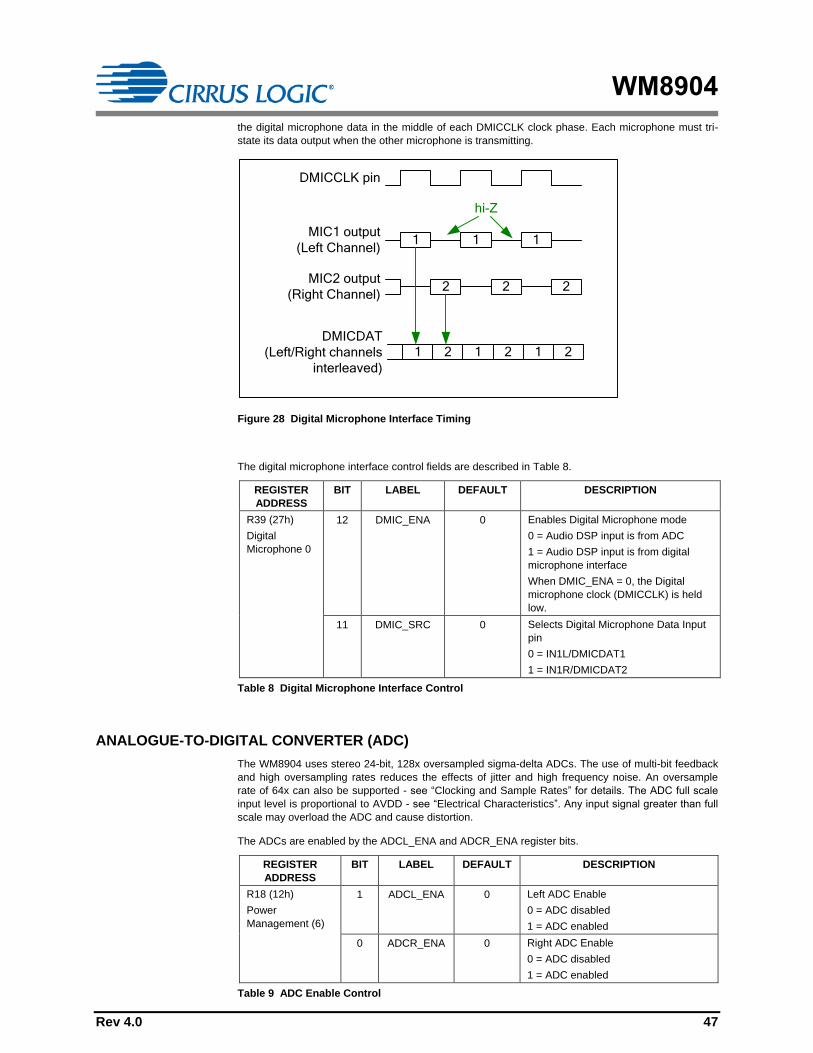
WM8904
Rev 4.0 47
the digital microphone data in the middle of each DMICCLK clock phase. Each microphone must tri-
state its data output when the other microphone is transmitting.
DMICCLK pin
DMICDAT
(Left/Right channels
interleaved)
1 2 1 2 1 2
MIC1 output
(Left Channel)1 1 1
MIC2 output
(Right Channel)2 2 2
hi-Z
Figure 28 Digital Microphone Interface Timing
The digital microphone interface control fields are described in Table 8.
REGISTER
ADDRESS
BIT LABEL DEFAULT DESCRIPTION
R39 (27h)
Digital
Microphone 0
12 DMIC_ENA 0 Enables Digital Microphone mode
0 = Audio DSP input is from ADC
1 = Audio DSP input is from digital
microphone interface
When DMIC_ENA = 0, the Digital
microphone clock (DMICCLK) is held
low.
11 DMIC_SRC 0 Selects Digital Microphone Data Input
pin
0 = IN1L/DMICDAT1
1 = IN1R/DMICDAT2
Table 8 Digital Microphone Interface Control
ANALOGUE-TO-DIGITAL CONVERTER (ADC)
The WM8904 uses stereo 24-bit, 128x oversampled sigma-delta ADCs. The use of multi-bit feedback
and high oversampling rates reduces the effects of jitter and high frequency noise. An oversample
rate of 64x can also be supported - see “Clocking and Sample Rates” for details. The ADC full scale
input level is proportional to AVDD - see “Electrical Characteristics”. Any input signal greater than full
scale may overload the ADC and cause distortion.
The ADCs are enabled by the ADCL_ENA and ADCR_ENA register bits.
REGISTER
ADDRESS
BIT LABEL DEFAULT DESCRIPTION
R18 (12h)
Power
Management (6)
1 ADCL_ENA 0 Left ADC Enable
0 = ADC disabled
1 = ADC enabled
0 ADCR_ENA 0 Right ADC Enable
0 = ADC disabled
1 = ADC enabled
Table 9 ADC Enable Control

WM8904
48 Rev 4.0
ADC DIGITAL VOLUME CONTROL
The output of the ADCs can be digitally amplified or attenuated over a range from -71.625dB to
+17.625dB in 0.375dB steps. The volume of each channel can be controlled separately. The gain for a
given eight-bit code is detailed in Table 11.
The ADC_VU bit controls the loading of digital volume control data. When ADC_VU is set to 0, the
ADCL_VOL or ADCR_VOL control data will be loaded into the respective control register, but will not
actually change the digital gain setting. Both left and right gain settings are updated when a 1 is
written to ADC_VU. This makes it possible to update the gain of both channels simultaneously.
REGISTER
ADDRESS
BIT LABEL DEFAULT DESCRIPTION
R36 (24h)
ADC Digital
Volume Left
8 ADC_VU 0 ADC Volume Update
Writing a 1 to this bit will cause left
and right ADC volume to be updated
simultaneously
7:0 ADCL_VOL
[7:0]
1100_0000
(0dB)
Left ADC Digital Volume
00h = Mute
01h = -71.625dB
02h = -71.250dB
… (0.375dB steps)
C0h = 0dB
… (0.375dB steps)
EFh to FFh = +17.625dB
(See Table 11 for volume range)
R37 (25h)
ADC Digital
Volume Right
8 ADC_VU 0 ADC Volume Update
Writing a 1 to this bit will cause left
and right ADC volume to be updated
simultaneously
7:0 ADCR_VOL
[7:0]
1100_0000
(0dB)
Right ADC Digital Volume
00h = Mute
01h = -71.625dB
02h = -71.250dB
… (0.375dB steps)
C0h = 0dB
… (0.375dB steps)
EFh to FFh = +17.625dB
(See Table 11 for volume range)
Table 10 ADC Digital Volume Control

WM8904
Rev 4.0 49
ADCL_VOL or
ADCR_VOL Volume (dB)
ADCL_VOL or
ADCR_VOL Volume (dB)
ADCL_VOL or
ADCR_VOL Volume (dB)
ADCL_VOL or
ADCR_VOL Volume (dB)
0h MUTE 40h -48.000 80h -24.000 C0h 0.000
1h -71.625 41h -47.625 81h -23.625 C1h 0.375
2h -71.250 42h -47.250 82h -23.250 C2h 0.750
3h -70.875 43h -46.875 83h -22.875 C3h 1.125
4h -70.500 44h -46.500 84h -22.500 C4h 1.500
5h -70.125 45h -46.125 85h -22.125 C5h 1.875
6h -69.750 46h -45.750 86h -21.750 C6h 2.250
7h -69.375 47h -45.375 87h -21.375 C7h 2.625
8h -69.000 48h -45.000 88h -21.000 C8h 3.000
9h -68.625 49h -44.625 89h -20.625 C9h 3.375
Ah -68.250 4Ah -44.250 8Ah -20.250 CAh 3.750
Bh -67.875 4Bh -43.875 8Bh -19.875 CBh 4.125
Ch -67.500 4Ch -43.500 8Ch -19.500 CCh 4.500
Dh -67.125 4Dh -43.125 8Dh -19.125 CDh 4.875
Eh -66.750 4Eh -42.750 8Eh -18.750 CEh 5.250
Fh -66.375 4Fh -42.375 8Fh -18.375 CFh 5.625
10h -66.000 50h -42.000 90h -18.000 D0h 6.000
11h -65.625 51h -41.625 91h -17.625 D1h 6.375
12h -65.250 52h -41.250 92h -17.250 D2h 6.750
13h -64.875 53h -40.875 93h -16.875 D3h 7.125
14h -64.500 54h -40.500 94h -16.500 D4h 7.500
15h -64.125 55h -40.125 95h -16.125 D5h 7.875
16h -63.750 56h -39.750 96h -15.750 D6h 8.250
17h -63.375 57h -39.375 97h -15.375 D7h 8.625
18h -63.000 58h -39.000 98h -15.000 D8h 9.000
19h -62.625 59h -38.625 99h -14.625 D9h 9.375
1Ah -62.250 5Ah -38.250 9Ah -14.250 DAh 9.750
1Bh -61.875 5Bh -37.875 9Bh -13.875 DBh 10.125
1Ch -61.500 5Ch -37.500 9Ch -13.500 DCh 10.500
1Dh -61.125 5Dh -37.125 9Dh -13.125 DDh 10.875
1Eh -60.750 5Eh -36.750 9Eh -12.750 DEh 11.250
1Fh -60.375 5Fh -36.375 9Fh -12.375 DFh 11.625
20h -60.000 60h -36.000 A0h -12.000 E0h 12.000
21h -59.625 61h -35.625 A1h -11.625 E1h 12.375
22h -59.250 62h -35.250 A2h -11.250 E2h 12.750
23h -58.875 63h -34.875 A3h -10.875 E3h 13.125
24h -58.500 64h -34.500 A4h -10.500 E4h 13.500
25h -58.125 65h -34.125 A5h -10.125 E5h 13.875
26h -57.750 66h -33.750 A6h -9.750 E6h 14.250
27h -57.375 67h -33.375 A7h -9.375 E7h 14.625
28h -57.000 68h -33.000 A8h -9.000 E8h 15.000
29h -56.625 69h -32.625 A9h -8.625 E9h 15.375
2Ah -56.250 6Ah -32.250 AAh -8.250 EAh 15.750
2Bh -55.875 6Bh -31.875 ABh -7.875 EBh 16.125
2Ch -55.500 6Ch -31.500 ACh -7.500 ECh 16.500
2Dh -55.125 6Dh -31.125 ADh -7.125 EDh 16.875
2Eh -54.750 6Eh -30.750 AEh -6.750 EEh 17.250
2Fh -54.375 6Fh -30.375 AFh -6.375 EFh 17.625
30h -54.000 70h -30.000 B0h -6.000 F0h 17.625
31h -53.625 71h -29.625 B1h -5.625 F1h 17.625
32h -53.250 72h -29.250 B2h -5.250 F2h 17.625
33h -52.875 73h -28.875 B3h -4.875 F3h 17.625
34h -52.500 74h -28.500 B4h -4.500 F4h 17.625
35h -52.125 75h -28.125 B5h -4.125 F5h 17.625
36h -51.750 76h -27.750 B6h -3.750 F6h 17.625
37h -51.375 77h -27.375 B7h -3.375 F7h 17.625
38h -51.000 78h -27.000 B8h -3.000 F8h 17.625
39h -50.625 79h -26.625 B9h -2.625 F9h 17.625
3Ah -50.250 7Ah -26.250 BAh -2.250 FAh 17.625
3Bh -49.875 7Bh -25.875 BBh -1.875 FBh 17.625
3Ch -49.500 7Ch -25.500 BCh -1.500 FCh 17.625
3Dh -49.125 7Dh -25.125 BDh -1.125 FDh 17.625
3Eh -48.750 7Eh -24.750 BEh -0.750 FEh 17.625
3Fh -48.375 7Fh -24.375 BFh -0.375 FFh 17.625
Table 11 ADC Digital Volume Range

WM8904
50 Rev 4.0
HIGH PASS FILTER
A digital high pass filter is applied by default to the ADC path to remove DC offsets. This filter can also
be programmed to remove low frequency noise in voice applications (e.g. wind noise or mechanical
vibration). This filter is controlled using the ADC_HPF and ADC_HPF_CUT register bits.
In hi-fi mode the high pass filter is optimised for removing DC offsets without degrading the bass
response and has a cut-off frequency of 3.7Hz at fs=44.1kHz.
In voice mode the high pass filter is optimised for voice communication and it is recommended to
program the cut-off frequency below 300Hz (e.g. ADC_HPF_CUT=11 at fs=8kHz or
ADC_HPF_CUT=10 at fs=16kHz).
REGISTER
ADDRESS BIT LABEL DEFAULT DESCRIPTION
R38 (26h)
ADC Digital
0
6:5 ADC_HPF_C
UT [1:0]
00 ADC Digital High Pass Filter Cut-Off
Frequency (fc)
00 = Hi-fi mode (fc=4Hz at fs=48kHz)
01 = Voice mode 1 (fc=127Hz at
fs=16kHz)
10 = Voice mode 2 (fc=130Hz at fs=8kHz)
11 = Voice mode 3 (fc=267Hz at fs=8kHz)
(Note: fc scales with sample rate. See
Table 13 for cut-off frequencies at all
supported sample rates)
4 ADC_HPF 1 ADC Digital High Pass Filter Enable
0 = disabled
1 = enabled
Table 12 ADC Digital 0 Register
Sample
Frequency
(kHz)
CUT-OFF FREQUENCY (Hz)
ADC_HPF_CUT
=00
ADC_HPF_CUT
=01
ADC_HPF_CUT
=10
ADC_HPF_CUT
=11
8.000 0.7 64 130 267
11.025 0.9 88 178 367
16.000 1.3 127 258 532
22.050 1.9 175 354 733
24.000 2.0 190 386 798
32.000 2.7 253 514 1063
44.100 3.7 348 707 1464
48.000 4.0 379 770 1594
Table 13 ADC High Pass Filter Cut-Off Frequencies
The high pass filter characteristics are shown in the “Digital Filter Characteristics” section.

WM8904
Rev 4.0 51
ADC OVERSAMPLING RATIO (OSR)
The ADC oversampling rate is programmable to allow power consumption versus audio performance
trade-offs. The default oversampling rate is high for best performance; using the lower OSR setting
reduces ADC power consumption.
To ensure specified ADC performance, the ADC Bias Control bits in register R198 must be set
correctly, depending on the ADC_OSR128 value, as described in Table 14.
REGISTER
ADDRESS
BIT LABEL DEFAULT DESCRIPTION
R10 (0Ah)
Analogue ADC
0
0 ADC_OSR128 1 ADC Oversampling Ratio
0 = Low Power (64 x fs)
1 = High Performance (128 x fs)
R198 (C6h)
ADC Test 0
2 ADC_128_OSR_
TST_MODE
0 ADC Bias Control (1)
Set this bit to 1 in ADC 64fs mode
(ADC_OSR128 = 0).
Set this bit to 0 in ADC 128fs mode
(ADC_OSR128 = 1).
0 ADC_BIASX1P5 0 ADC Bias Control (2)
Set this bit to 1 in ADC 64fs mode
(ADC_OSR128 = 0).
Set this bit to 0 in ADC 128fs mode
(ADC_OSR128 = 1).
Table 14 ADC Oversampling Ratio
DYNAMIC RANGE CONTROL (DRC)
The dynamic range controller (DRC) is a circuit which can be enabled in the digital data path of either
the ADCs or the DACs. The function of the DRC is to adjust the signal gain in conditions where the
input amplitude is unknown or varies over a wide range, e.g. when recording from microphones built
into a handheld system. The DRC can apply Compression and Automatic Level Control to the signal
path. It incorporates ‘anti-clip’ and ‘quick release’ features for handling transients in order to improve
intelligibility in the presence of loud impulsive noises.
The DRC is enabled by DRC_ENA, as shown in Table 15. It can be enabled in the ADC digital path or
in the DAC digital path, under the control of the DRC_DAC_PATH register bit. Note that the DRC can
be active in only one of these paths at any time.
REGISTER
ADDRESS
BIT LABEL DEFAULT DESCRIPTION
R40 (28h)
DRC Control 0
15 DRC_ENA 0 DRC enable
0 = disabled
1 = enabled
14 DRC_DAC_PAT
H
0 DRC path select
0 = ADC path
1 = DAC path
Table 15 DRC Enable

WM8904
52 Rev 4.0
COMPRESSION/LIMITING CAPABILITIES
The DRC supports two different compression regions, separated by a “knee” at input amplitude T. For
signals above the knee, the compression slope DRC_HI_COMP applies; for signals below the knee,
the compression slope DRC_LO_COMP applies.
The overall DRC compression characteristic in “steady state” (i.e. where the input amplitude is near-
constant) is illustrated in Figure 29.
DRC_KNEE_IP
(Y0)
0dB
DRC_HI_COMP
DRC_LO_COMP
DRC Input Amplitude (dB)
DRC Output Amplitude (dB)
DRC_KNEE_OP
“knee”
Figure 29 DRC Compression Characteristic
The slope of the DRC response is determined by register fields DRC_HI_COMP and DRC_LO_COMP
respectively. A slope of 1 indicates constant gain in this region. A slope less than 1 represents
compression (i.e. a change in input amplitude produces only a smaller change in output amplitude). A
slope of 0 indicates that the target output amplitude is the same across a range of input amplitudes;
this is infinite compression.
The “knee” in Figure 29 is represented by register fields DRC_KNEE_IP and DRC_KNEE_OP.
Parameter Y0, the output level for a 0dB input, is not specified directly, but can be calculated from the
other parameters, using the equation
Y0 = DRC_KNEE_OP – (DRC_KNEE_IP * DRC_HI_COMP)
The DRC Compression parameters are defined in Table 16.
REGISTER
ADDRESS
BIT LABEL DEFAULT DESCRIPTION
R43 (2Bh)
DRC Control 3
10:5 DRC_KNEE_IP
[5:0]
00_0000 Input signal at the Compressor
'knee'.
000000 = 0dB
000001 = -0.75dB
000010 = -1.5dB
… (-0.75dB steps)
111100 = -45dB
111101 to 111111 = Reserved
4:0 DRC_KNEE_OP
[4:0]
0_0000 Output signal at the Compressor
'knee'.
00000 = 0dB
00001 = -0.75dB
00010 = -1.5dB
… (-0.75dB steps)
11110 = -22.5dB
11111 = Reserved

WM8904
Rev 4.0 53
REGISTER
ADDRESS
BIT LABEL DEFAULT DESCRIPTION
R42 (2Ah)
DRC Control 2
5:3 DRC_HI_COMP
[2:0]
000 Compressor slope (upper region)
000 = 1 (no compression)
001 = 1/2
010 = 1/4
011 = 1/8
100 = 1/16
101 = 0
110 to 111 = Reserved
2:0 DRC_LO_COMP
[2:0]
000 Compressor slope (lower region)
000 = 1 (no compression)
001 = 1/2
010 = 1/4
011 = 1/8
100 = 0
101 to 111 = Reserved
Table 16 DRC Compression Control
GAIN LIMITS
The minimum and maximum gain applied by the DRC is set by register fields DRC_MINGAIN and
DRC_MAXGAIN. These limits can be used to alter the DRC response from that illustrated in Figure
29. If the range between maximum and minimum gain is reduced, then the extent of the dynamic
range control is reduced. The maximum gain prevents quiet signals (or silence) from being
excessively amplified.
REGISTER
ADDRESS
BIT LABEL DEFAULT DESCRIPTION
R41 (29h)
DRC Control 1
3:2 DRC_MINGAIN [1:0] 10 Minimum gain the DRC can use
to attenuate audio signals
00 = 0dB (default)
01 = -6dB
10 = -12dB
11 = -18dB
1:0 DRC_MAXGAIN
[1:0]
00 Maximum gain the DRC can use
to boost audio signals
00 = 12dB
01 = 18dB (default)
10 = 24dB
11 = 36dB
Table 17 DRC Gain Limits
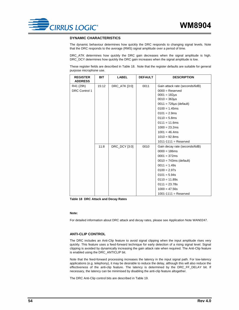
WM8904
54 Rev 4.0
DYNAMIC CHARACTERISTICS
The dynamic behaviour determines how quickly the DRC responds to changing signal levels. Note
that the DRC responds to the average (RMS) signal amplitude over a period of time.
DRC_ATK determines how quickly the DRC gain decreases when the signal amplitude is high.
DRC_DCY determines how quickly the DRC gain increases when the signal amplitude is low.
These register fields are described in Table 18. Note that the register defaults are suitable for general
purpose microphone use.
REGISTER
ADDRESS
BIT LABEL DEFAULT DESCRIPTION
R41 (29h)
DRC Control 1
15:12 DRC_ATK [3:0] 0011 Gain attack rate (seconds/6dB)
0000 = Reserved
0001 = 182µs
0010 = 363µs
0011 = 726µs (default)
0100 = 1.45ms
0101 = 2.9ms
0110 = 5.8ms
0111 = 11.6ms
1000 = 23.2ms
1001 = 46.4ms
1010 = 92.8ms
1011-1111 = Reserved
11:8 DRC_DCY [3:0] 0010 Gain decay rate (seconds/6dB)
0000 = 186ms
0001 = 372ms
0010 = 743ms (default)
0011 = 1.49s
0100 = 2.97s
0101 = 5.94s
0110 = 11.89s
0111 = 23.78s
1000 = 47.56s
1001-1111 = Reserved
Table 18 DRC Attack and Decay Rates
Note:
For detailed information about DRC attack and decay rates, please see Application Note WAN0247.
ANTI-CLIP CONTROL
The DRC includes an Anti-Clip feature to avoid signal clipping when the input amplitude rises very
quickly. This feature uses a feed-forward technique for early detection of a rising signal level. Signal
clipping is avoided by dynamically increasing the gain attack rate when required. The Anti-Clip feature
is enabled using the DRC_ANTICLIP bit.
Note that the feed-forward processing increases the latency in the input signal path. For low-latency
applications (e.g. telephony), it may be desirable to reduce the delay, although this will also reduce the
effectiveness of the anti-clip feature. The latency is determined by the DRC_FF_DELAY bit. If
necessary, the latency can be minimised by disabling the anti-clip feature altogether.
The DRC Anti-Clip control bits are described in Table 19.

WM8904
Rev 4.0 55
REGISTER
ADDRESS
BIT LABEL DEFAULT DESCRIPTION
R40 (28h)
DRC Control 0
5 DRC_FF_DELAY 1 Feed-forward delay for anti-clip
feature
0 = 5 samples
1 = 9 samples
Time delay can be calculated as 5/fs
or 9/ fs, where fs is the sample rate.
1 DRC_ANTICLIP 1 Anti-clip enable
0 = disabled
1 = enabled
Table 19 DRC Anti-Clip Control
Note that the Anti-Clip feature operates entirely in the digital domain. It cannot be used to prevent
signal clipping in the analogue domain nor in the source signal. Analogue clipping can only be
prevented by reducing the analogue signal gain or by adjusting the source signal.
QUICK RELEASE CONTROL
The DRC includes a Quick-Release feature to handle short transient peaks that are not related to the
intended source signal. For example, in handheld microphone recording, transient signal peaks
sometimes occur due to user handling, key presses or accidental tapping against the microphone.
The Quick Release feature ensures that these transients do not cause the intended signal to be
masked by the longer time constants of DRC_DCY.
The Quick-Release feature is enabled by setting the DRC_QR bit. When this bit is enabled, the DRC
measures the crest factor (peak to RMS ratio) of the input signal. A high crest factor is indicative of a
transient peak that may not be related to the intended source signal. If the crest factor exceeds the
level set by DRC_QR_THR, then the normal decay rate (DRC_DCY) is ignored and a faster decay
rate (DRC _QR_DCY) is used instead.
The DRC Quick-Release control bits are described in Table 20.
REGISTER
ADDRESS
BIT LABEL DEFAULT DESCRIPTION
R40 (28h)
DRC Control 0
2 DRC_QR 1 Quick release enable
0 = disabled
1 = enabled
R41 (29h)
DRC Control 1
7:6 DRC_QR_THR
[1:0]
01 Quick release crest factor threshold
00 = 12dB
01 = 18dB (default)
10 = 24dB
11 = 30dB
5:4 DRC_QR_DCY
[1:0]
00 Quick release decay rate
(seconds/6dB)
00 = 0.725ms (default)
01 = 1.45ms
10 = 5.8ms
11 = Reserved
Table 20 DRC Quick-Release Control

WM8904
56 Rev 4.0
GAIN SMOOTHING
The DRC includes a gain smoothing filter in order to prevent gain ripples. A programmable level of
hysteresis is also used to control the DRC gain. This improves the handling of very low frequency
input signals whose period is close to the DRC attack/decay time. DRC Gain Smoothing is enabled by
default and it is recommended to use the default register settings.
The extent of the gain smoothing filter may be adjusted or disabled using the control fields described
in Table 21.
REGISTER
ADDRESS
BIT LABEL DEFAULT DESCRIPTION
R40 (28h)
DRC Control 0
12:11 DRC_GS_HYST
_LVL [1:0]
00 Gain smoothing hysteresis
threshold
00 = Low
01 = Medium (recommended)
10 = High
11 = Reserved
3 DRC_GS_ENA 1 Gain smoothing enable
0 = disabled
1 = enabled
0 DRC_GS_HYST 1 Gain smoothing hysteresis enable
0 = disabled
1 = enabled
Table 21 DRC Gain Smoothing
INITIALISATION
When the DRC is initialised, the gain is set to the level determined by the DRC_STARTUP_GAIN
register field. The default setting is 0dB, but values from -3dB to +6dB are available, as described in
Table 22.
REGISTER
ADDRESS
BIT LABEL DEFAULT DESCRIPTION
R40 (28h)
DRC Control 0
10:6 DRC_STARTUP_
GAIN [4:0]
00110 Initial gain at DRC start-up
00000 = -3dB
00001 = -2.5dB
00010 = -2dB
00011 = -1.5dB
00100 = -1dB
00101 = -0.5dB
00110 = 0dB (default)
00111 = 0.5dB
01000 = 1dB
01001 = 1.5dB
01010 = 2dB
01011 = 2.5dB
01100 = 3dB
01101 = 3.5dB
01110 = 4dB
01111 = 4.5dB
10000 = 5dB
10001 = 5.5dB
10010 = 6dB
10011 to 11111 = Reserved
Table 22 DRC Initialisation

WM8904
Rev 4.0 57
RETUNETM MOBILE PARAMETRIC EQUALIZER (EQ)
The ReTuneTM Mobile Parametric Equaliser is a circuit that can be enabled in the DAC path. The
function of the EQ is to adjust the frequency characteristic of the output to compensate for unwanted
frequency characteristics in the loudspeaker (or other output transducer). It can also be used to tailor
the response according to user preferences, for example to accentuate or attenuate specific
frequency bands to emulate different sound profiles or environments such as concert hall, rock etc.
The EQ is enabled using the EQ_ENA bit as shown in Table 23.
REGISTER
ADDRESS
BIT LABEL DEFAULT DESCRIPTION
R134 (86h)
EQ1
0 EQ_ENA 0 EQ enable
0 = EQ disabled
1 = EQ enabled
Table 23 ReTuneTM Mobile Parametric EQ Enable
The EQ can be configured to operate in two modes - “Default” mode or “ReTuneTM Mobile” mode.
DEFAULT MODE (5-BAND PARAMETRIC EQ)
In default mode, the cut-off / centre frequencies are fixed as per Table 24. The filter bandwidths are
also fixed in default mode. The gain of the individual bands (-12dB to +12dB) can be controlled as
described in Table 25.
Note that the cut-off / centre frequencies noted in Table 24 are applicable to a DAC Sample Rate of
48kHz. When using other sample rates, these frequencies will be scaled in proportion to the selected
sample rate.
EQ BAND CUT-OFF/CENTRE
FREQUENCY
1 100 Hz
2 300 Hz
3 875 Hz
4 2400 Hz
5 6900 Hz
Table 24 EQ Band Cut-off / Centre Frequencies
REGISTER
ADDRESS
BIT LABEL DEFAULT DESCRIPTION
R135 (87h)
EQ2
4:0 EQ_B1_GAIN [4:0] 01100b
(0dB)
EQ Band 1 Gain
(see Table 26 for gain range)
R136 (88h)
EQ3
4:0 EQ_B2_GAIN [4:0] 01100b
(0dB)
EQ Band 2 Gain
(see Table 26 for gain range)
R137 (89h)
EQ4
4:0 EQ_B3_GAIN [4:0] 01100b
(0dB)
EQ Band 3 Gain
(see Table 26 for gain range)
R138 (8Ah)
EQ5
4:0 EQ_B4_GAIN [4:0] 01100b
(0dB)
EQ Band 4 Gain
(see Table 26 for gain range)
R139 (8Bh)
EQ6
4:0 EQ_B5_GAIN [4:0] 01100b
(0dB)
EQ Band 5 Gain
(see Table 26 for gain range)
Table 25 EQ Band Gain Control

WM8904
58 Rev 4.0
EQ GAIN SETTING GAIN (DB)
00000 -12
00001 -11
00010 -10
00011 -9
00100 -8
00101 -7
00110 -6
00111 -5
01000 -4
01001 -3
01010 -2
01011 -1
01100 0
01101 +1
01110 +2
01111 +3
10000 +4
10001 +5
10010 +6
10011 +7
10100 +8
10101 +9
10110 +10
10111 +11
11000 +12
11001 to 11111 Reserved
Table 26 EQ Gain Control
RETUNETM MOBILE MODE
ReTuneTM Mobile mode provides a comprehensive facility for the user to define the cut-off/centre
frequencies and filter bandwidth for each EQ band, in addition to the gain controls already described.
This enables the EQ to be accurately customised for a specific transducer characteristic or desired
sound profile.
The EQ enable and EQ gain controls are the same as defined for the default mode. The additional
coefficients used in ReTuneTM Mobile mode are held in registers R140 to R157. These coefficients are
derived using tools provided in the WISCE™ evaluation board control software.
Please contact your local Cirrus Logic representative for more details.
EQ FILTER CHARACTERISTICS
The filter characteristics for each frequency band are shown in Figure 30 to Figure 34. These figures
show the frequency response for all available gain settings, using default cut-off/centre frequencies
and bandwidth.

WM8904
Rev 4.0 59
-15
-10
-5
0
5
10
15
1 10 100 1000 10000 100000
Frequency (Hz)
Ga
in (
dB
)
-15
-10
-5
0
5
10
15
1 10 100 1000 10000 100000
Frequency (Hz)
Ga
in (
dB
)
Figure 30 EQ Band 1 – Low Freq Shelf Filter Response Figure 31 EQ Band 2 – Peak Filter Response
-15
-10
-5
0
5
10
15
1 10 100 1000 10000 100000
Frequency (Hz)
Ga
in (
dB
)
-15
-10
-5
0
5
10
15
1 10 100 1000 10000 100000
Frequency (Hz)
Ga
in (
dB
)
Figure 32 EQ Band 3 – Peak Filter Response Figure 33 EQ Band 4 – Peak Filter Response
-15
-10
-5
0
5
10
15
1 10 100 1000 10000 100000
Frequency (Hz)
Ga
in (
dB
)
Figure 34 EQ Band 5 – High Freq Shelf Filter Response

WM8904
60 Rev 4.0
DIGITAL MIXING
The ADC and DAC data can be combined in various ways to support a range of different usage
modes.
Data from either of the two ADCs can be routed to either the left or the right channel of the digital
audio interface. In addition, data from either of the digital audio interface channels can be routed to
either the left or the right DAC. See "Digital Audio Interface" for more information on the audio
interface.
The WM8904 provides a Dynamic Range Control (DRC) feature, which can apply compression and
gain adjustment in the digital domain to either the ADC or DAC signal path. This is effective in
controlling signal levels under conditions where input amplitude is unknown or varies over a wide
range.
The DACs can be configured as a mono mix of the two audio channels. Digital sidetone from the
ADCs can also be selectively mixed into the DAC output path.
DIGITAL MIXING PATHS
Figure 35 shows the digital mixing paths available in the WM8904 digital core.
AD
CD
AT
BC
LK
DA
CD
AT
LR
CL
K
DAC L
DAC R
ReTune Mobile
Parametric
Equalizer
L R
R L
L/R SWAP
Dynamic Range
Controller
Dynamic Range Control
(DRC) available on ADC
or DAC channels, not both.
Dynamic Range
Controller
+
DIGITAL AUDIO
INTERFACEA-law and -law Support
TDM Support
MONO MIX
+
L R
R L
AIFADCL_SRC
AIFADCR_SRC
ADCL_DATINV
ADCR_DATINV
AIFDACL_SRC
AIFDACR_SRC
DACL_DATINV
DACR_DATINV
DAC_VU
DACL_VOL[7:0]
DACR_VOL[7:0]
DAC_MUTE
DAC_BOOST[1:0]
DAC_MUTERATE
DAC_UNMUTE_RAMP
ADC_VU
ADCL_VOL[7:0]
ADCR_VOL[7:0]
ADCL_ENA
DACL_ENA
DACR_ENA
DEEMPH[1:0]
DAC_COMP
DAC_COMPMODE
ADC_COMP
ADC_COMPMODE
AIFDAC_TDM
AIFDAC_TDM_CHAN
AIFADC_TDM
AIFADC_TDM_CHAN
AIF_WL[1:0]
AIF_FMT[1:0]
LOOPBACK
ADC_HPF
ADC_HPF_CUT[1:0]
ADCL_DAC_SVOL[3:0]
ADCR_DAC_SVOL[3:0]
DAC_SB_FILT
DAC_MONO
ADC_TO_DACL[1:0]
ADC_TO_DACR[1:0]
DMIC_ENA
ADCR_ENA
ADC R
ADC L
DMIC interface
Figure 35 Digital Mixing Paths

WM8904
Rev 4.0 61
The polarity of each ADC output signal can be changed under software control using the
ADCL_DATINV and ADCR_DATINV register bits. The AIFADCL_SRC and AIFADCR_SRC register
bits may be used to select which ADC is used for the left and right digital audio interface data. These
register bits are described in Table 27.
REGISTER
ADDRESS
BIT LABEL DEFAULT DESCRIPTION
R24 (18h)
Audio
Interface 0
7 AIFADCL_SRC 0 Left Digital Audio interface source
0 = Left ADC data is output on left
channel
1 = Right ADC data is output on left
channel
6 AIFADCR_SRC 1 Right Digital Audio interface source
0 = Left ADC data is output on right
channel
1 = Right ADC data is output on right
channel
R38 (26h)
ADC Digital
0
1 ADCL_DATINV 0 Left ADC Invert
0 = Left ADC output not inverted
1 = Left ADC output inverted
0 ADCR_DATINV 0 Right ADC Invert
0 = Right ADC output not inverted
1 = Right ADC output inverted
Table 27 ADC Routing and Control
The input data source for each DAC can be changed under software control using register bits
AIFDACL_SRC and AIFDACR_SRC. The polarity of each DAC input may also be modified using
register bits DACL_DATINV and DACR_DATINV. These register bits are described in Table 28.
REGISTER
ADDRESS
BIT LABEL DEFAULT DESCRIPTION
R24 (18h)
Audio
Interface 0
12 DACL_DATINV 0 Left DAC Invert
0 = Left DAC output not inverted
1 = Left DAC output inverted
11 DACR_DATINV 0 Right DAC Invert
0 = Right DAC output not inverted
1 = Right DAC output inverted
5 AIFDACL_SRC 0 Left DAC Data Source Select
0 = Left DAC outputs left interface data
1 = Left DAC outputs right interface data
4 AIFDACR_SRC 1 Right DAC Data Source Select
0 = Right DAC outputs left interface data
1 = Right DAC outputs right interface
data
Table 28 DAC Routing and Control

WM8904
62 Rev 4.0
DAC INTERFACE VOLUME BOOST
A digital gain function is available at the audio interface to boost the DAC volume when a small signal
is received on DACDAT. This is controlled using register bits DAC_BOOST [1:0]. To prevent clipping
at the DAC input, this function should not be used when the boosted DAC data is expected to be
greater than 0dBFS.
The digital interface volume is controlled as shown in Table 29.
REGISTER
ADDRESS
BIT LABEL DEFAULT DESCRIPTION
R24 (18h)
Audio
Interface 0
10:9 DAC_BOOST
[1:0]
00 DAC Input Volume Boost
00 = 0dB
01 = +6dB (Input data must not
exceed -6dBFS)
10 = +12dB (Input data must not
exceed -12dBFS)
11 = +18dB (Input data must not
exceed -18dBFS)
Table 29 DAC Interface Volume Boost
DIGITAL SIDETONE
A digital sidetone is available when ADCs and DACs are operating at the same sample rate. Digital
data from either left or right ADC can be mixed with the audio interface data on the left and right DAC
channels. Sidetone data is taken from the ADC high pass filter output, to reduce low frequency noise
in the sidetone (e.g. wind noise or mechanical vibration).
When using the digital sidetone, it is recommended that the ADCs are enabled before un-muting the
DACs to prevent pop noise. The DAC volumes and sidetone volumes should be set to an appropriate
level to avoid clipping at the DAC input.
When digital sidetone is used, it is recommended that the Charge Pump operates in Register Control
mode only (CP_DYN_PWR = 0). See “Charge Pump” for details.
The digital sidetone is controlled as shown in Table 30.
REGISTER
ADDRESS
BIT LABEL DEFAULT DESCRIPTION
R32 (20h)
DAC Digital
0
11:8 ADCL_DAC_SVOL
[3:0]
0000 Left Digital Sidetone Volume
(See Table 31 for volume range)
7:4 ADCR_DAC_SVOL
[3:0]
0000 Right Digital Sidetone Volume
(See Table 31 for volume range)
3:2 ADC_TO_DACL
[1:0]
00 Left DAC Digital Sidetone Source
00 = No sidetone
01 = Left ADC
10 = Right ADC
11 = Reserved
1:0 ADC_TO_DACR
[1:0]
00 Right DAC Digital Sidetone Source
00 = No sidetone
01 = Left ADC
10 = Right ADC
11 = Reserved
Table 30 Digital Sidetone Control

WM8904
Rev 4.0 63
The digital sidetone volume settings are shown in Table 31.
ADCL_DAC_SVOL
OR
ADCR_DAC_SVOL
SIDETONE VOLUME
0000 -36
0001 -33
0010 -30
0011 -27
0100 -24
0101 -21
0110 -18
0111 -15
1000 -12
1001 -9
1010 -6
1011 -3
1100 0
1101 0
1110 0
1111 0
Table 31 Digital Sidetone Volume

WM8904
64 Rev 4.0
DIGITAL-TO-ANALOGUE CONVERTER (DAC)
The WM8904 DACs receive digital input data from the DACDAT pin and via the digital sidetone path
(see “Digital Mixing” section). The digital audio data is converted to oversampled bit streams in the on-
chip, true 24-bit digital interpolation filters. The bitstream data enters two multi-bit, sigma-delta DACs,
which convert them to high quality analogue audio signals. The Wolfson SmartDAC™ architecture
offers reduced power consumption, whilst also delivering a reduction in high frequency noise and
sensitivity to clock jitter. It also uses a Dynamic Element Matching technique for high linearity and low
distortion.
The analogue outputs from the DACs are sent directly to the output PGAs (see “Output Signal Path”).
The DACs are enabled by the DACL_ENA and DACR_ENA register bits.
REGISTER
ADDRESS
BIT LABEL DEFAULT DESCRIPTION
R18 (12h)
Power
Management
6
3 DACL_ENA 0 Left DAC Enable
0 = DAC disabled
1 = DAC enabled
2 DACR_ENA 0 Right DAC Enable
0 = DAC disabled
1 = DAC enabled
Table 32 DAC Enable Control
DAC DIGITAL VOLUME CONTROL
The output level of each DAC can be controlled digitally over a range from -71.625dB to 0dB in
0.375dB steps. The level of attenuation for an eight-bit code is detailed in Table 34.
The DAC_VU bit controls the loading of digital volume control data. When DAC_VU is set to 0, the
DACL_VOL or DACR_VOL control data is loaded into the respective control register, but does not
actually change the digital gain setting. Both left and right gain settings are updated when a 1 is
written to DAC_VU. This makes it possible to update the gain of both channels simultaneously.
REGISTER
ADDRESS
BIT LABEL DEFAULT DESCRIPTION
R30 (1Eh)
DAC Digital
Volume Left
8 DAC_VU N/A DAC Volume Update
Writing a 1 to this bit causes left
and right DAC volume to be
updated simultaneously
7:0 DACL_VOL [7:0] 1100_0000
(0dB)
Left DAC Digital Volume
00h = Mute
01h = -71.625dB
02h = -71.250dB
… (0.375dB steps)
C0h to FFh = 0dB
(See Table 34 for volume range)
R31 (1Fh)
DAC Digital
Volume Right
8 DAC_VU N/A DAC Volume Update
Writing a 1 to this bit causes left
and right DAC volume to be
updated simultaneously
7:0 DACR_VOL [7:0] 1100_0000
(0dB)
Right DAC Digital Volume
00h = Mute
01h = -71.625dB
02h = -71.250dB
… (0.375dB steps)
C0h to FFh = 0dB
(See Table 34 for volume range)
Table 33 DAC Digital Volume Control
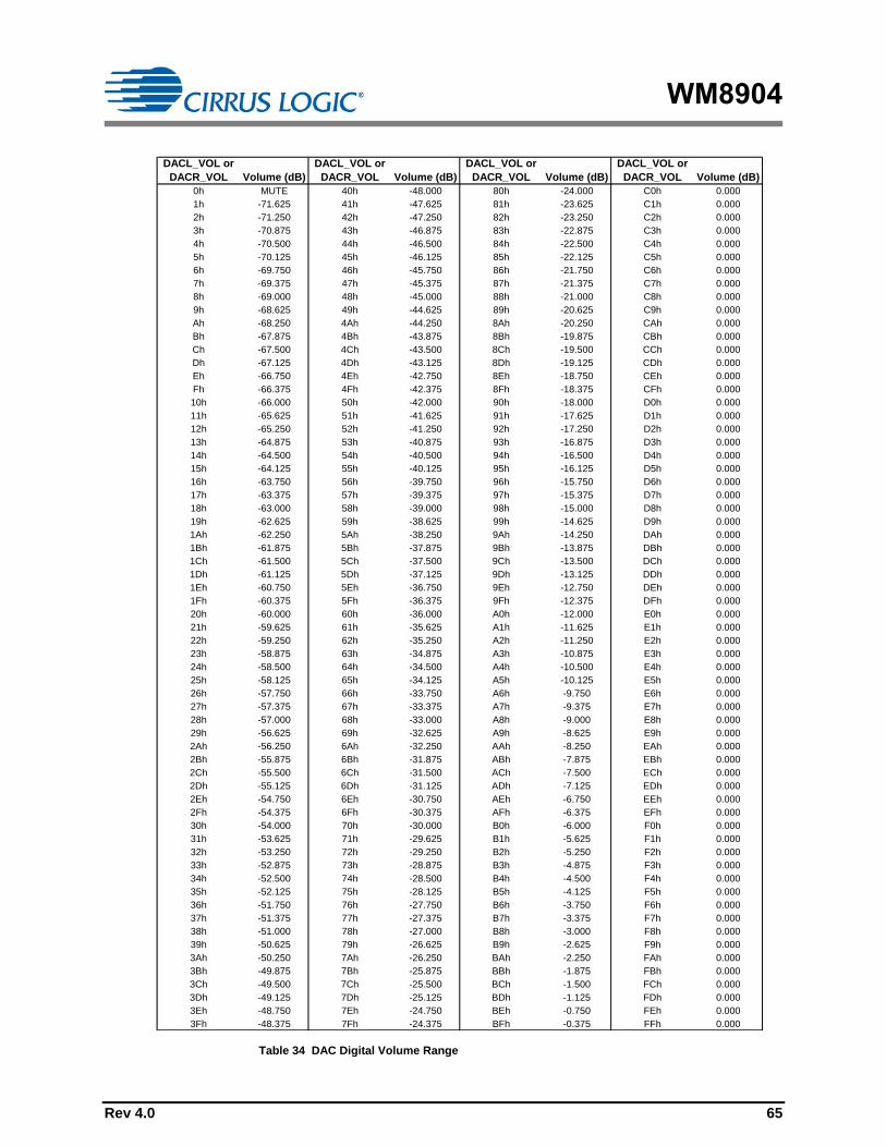
WM8904
Rev 4.0 65
DACL_VOL or
DACR_VOL Volume (dB)
DACL_VOL or
DACR_VOL Volume (dB)
DACL_VOL or
DACR_VOL Volume (dB)
DACL_VOL or
DACR_VOL Volume (dB)
0h MUTE 40h -48.000 80h -24.000 C0h 0.000
1h -71.625 41h -47.625 81h -23.625 C1h 0.000
2h -71.250 42h -47.250 82h -23.250 C2h 0.000
3h -70.875 43h -46.875 83h -22.875 C3h 0.000
4h -70.500 44h -46.500 84h -22.500 C4h 0.000
5h -70.125 45h -46.125 85h -22.125 C5h 0.000
6h -69.750 46h -45.750 86h -21.750 C6h 0.000
7h -69.375 47h -45.375 87h -21.375 C7h 0.000
8h -69.000 48h -45.000 88h -21.000 C8h 0.000
9h -68.625 49h -44.625 89h -20.625 C9h 0.000
Ah -68.250 4Ah -44.250 8Ah -20.250 CAh 0.000
Bh -67.875 4Bh -43.875 8Bh -19.875 CBh 0.000
Ch -67.500 4Ch -43.500 8Ch -19.500 CCh 0.000
Dh -67.125 4Dh -43.125 8Dh -19.125 CDh 0.000
Eh -66.750 4Eh -42.750 8Eh -18.750 CEh 0.000
Fh -66.375 4Fh -42.375 8Fh -18.375 CFh 0.000
10h -66.000 50h -42.000 90h -18.000 D0h 0.000
11h -65.625 51h -41.625 91h -17.625 D1h 0.000
12h -65.250 52h -41.250 92h -17.250 D2h 0.000
13h -64.875 53h -40.875 93h -16.875 D3h 0.000
14h -64.500 54h -40.500 94h -16.500 D4h 0.000
15h -64.125 55h -40.125 95h -16.125 D5h 0.000
16h -63.750 56h -39.750 96h -15.750 D6h 0.000
17h -63.375 57h -39.375 97h -15.375 D7h 0.000
18h -63.000 58h -39.000 98h -15.000 D8h 0.000
19h -62.625 59h -38.625 99h -14.625 D9h 0.000
1Ah -62.250 5Ah -38.250 9Ah -14.250 DAh 0.000
1Bh -61.875 5Bh -37.875 9Bh -13.875 DBh 0.000
1Ch -61.500 5Ch -37.500 9Ch -13.500 DCh 0.000
1Dh -61.125 5Dh -37.125 9Dh -13.125 DDh 0.000
1Eh -60.750 5Eh -36.750 9Eh -12.750 DEh 0.000
1Fh -60.375 5Fh -36.375 9Fh -12.375 DFh 0.000
20h -60.000 60h -36.000 A0h -12.000 E0h 0.000
21h -59.625 61h -35.625 A1h -11.625 E1h 0.000
22h -59.250 62h -35.250 A2h -11.250 E2h 0.000
23h -58.875 63h -34.875 A3h -10.875 E3h 0.000
24h -58.500 64h -34.500 A4h -10.500 E4h 0.000
25h -58.125 65h -34.125 A5h -10.125 E5h 0.000
26h -57.750 66h -33.750 A6h -9.750 E6h 0.000
27h -57.375 67h -33.375 A7h -9.375 E7h 0.000
28h -57.000 68h -33.000 A8h -9.000 E8h 0.000
29h -56.625 69h -32.625 A9h -8.625 E9h 0.000
2Ah -56.250 6Ah -32.250 AAh -8.250 EAh 0.000
2Bh -55.875 6Bh -31.875 ABh -7.875 EBh 0.000
2Ch -55.500 6Ch -31.500 ACh -7.500 ECh 0.000
2Dh -55.125 6Dh -31.125 ADh -7.125 EDh 0.000
2Eh -54.750 6Eh -30.750 AEh -6.750 EEh 0.000
2Fh -54.375 6Fh -30.375 AFh -6.375 EFh 0.000
30h -54.000 70h -30.000 B0h -6.000 F0h 0.000
31h -53.625 71h -29.625 B1h -5.625 F1h 0.000
32h -53.250 72h -29.250 B2h -5.250 F2h 0.000
33h -52.875 73h -28.875 B3h -4.875 F3h 0.000
34h -52.500 74h -28.500 B4h -4.500 F4h 0.000
35h -52.125 75h -28.125 B5h -4.125 F5h 0.000
36h -51.750 76h -27.750 B6h -3.750 F6h 0.000
37h -51.375 77h -27.375 B7h -3.375 F7h 0.000
38h -51.000 78h -27.000 B8h -3.000 F8h 0.000
39h -50.625 79h -26.625 B9h -2.625 F9h 0.000
3Ah -50.250 7Ah -26.250 BAh -2.250 FAh 0.000
3Bh -49.875 7Bh -25.875 BBh -1.875 FBh 0.000
3Ch -49.500 7Ch -25.500 BCh -1.500 FCh 0.000
3Dh -49.125 7Dh -25.125 BDh -1.125 FDh 0.000
3Eh -48.750 7Eh -24.750 BEh -0.750 FEh 0.000
3Fh -48.375 7Fh -24.375 BFh -0.375 FFh 0.000
Table 34 DAC Digital Volume Range

WM8904
66 Rev 4.0
DAC SOFT MUTE AND SOFT UN-MUTE
The WM8904 has a soft mute function. When enabled, this gradually attenuates the volume of the
DAC output. When soft mute is disabled, the gain will either gradually ramp back up to the digital gain
setting, or return instantly to the digital gain setting, depending on the DAC_UNMUTE_RAMP register
bit.
To mute the DAC, this function must be enabled by setting DAC_MUTE to 1.
Soft Mute Mode would typically be enabled (DAC_UNMUTE_RAMP = 1) when using DAC_MUTE
during playback of audio data so that when DAC_MUTE is subsequently disabled, the sudden volume
increase will not create pop noise by jumping immediately to the previous volume level (e.g. resuming
playback after pausing during a track).
Soft Mute Mode would typically be disabled (DAC_UNMUTE_RAMP = 0) when un-muting at the start
of a music file, in order that the first part of the track is not attenuated (e.g. when starting playback of a
new track, or resuming playback after pausing between tracks).
= [non-zero] = 00000000 = [non-zero]DACL_VOL or
DACR_VOL
DAC muting and un-muting using volume control bits
DACL_VOL and DACR_VOL.
DAC_MUTE = 0 DAC_MUTE = 1 DAC_MUTE = 0
DAC muting and un-muting using the DAC_MUTE bit.
If soft Mute Mode is not enabled (DAC_UNMUTE_RAMP = 0):
Setting the DAC_MUTE bit causes the volume to ramp down
at a rate controlled by DAC_MUTERATE.
Clearing the DAC_MUTE bit causes the volume to return to
the un-muted level immediately.
DAC_MUTE = 0 DAC_MUTE = 1 DAC_MUTE = 0
DAC muting and un-muting using the DAC_MUTE bit.
If soft Mute Mode is enabled (DAC_UNMUTE_RAMP = 1):
Setting the DAC_MUTE bit causes the volume to ramp down.
Clearing the DAC_MUTE bit causes the volume to ramp up to
the un-muted level at a rate controlled by DAC_MUTERATE.
Figure 36 DAC Mute Control
The volume ramp rate during soft mute and un-mute is controlled by the DAC_MUTERATE bit. Ramp
rates of fs/32 and fs/2 can be selected, as shown in Table 35. The ramp rate determines the rate at
which the volume is increased or decreased. The actual ramp time depends on the extent of the
difference between the muted and un-muted volume settings.

WM8904
Rev 4.0 67
REGISTER
ADDRESS
BIT LABEL DEFAULT DESCRIPTION
R33 (21h)
DAC Digital 1
10 DAC_MUTERA
TE
0 DAC Soft Mute Ramp Rate
0 = Fast ramp (fs/2, maximum ramp
time is 10.7ms at fs=48k)
1 = Slow ramp (fs/32, maximum ramp
time is 171ms at fs=48k)
9 DAC_UNMUTE
_RAMP
0 DAC Soft Mute Mode
0 = Disabling soft-mute
(DAC_MUTE=0) will cause the DAC
volume to change immediately to
DACL_VOL and DACR_VOL settings
1 = Disabling soft-mute
(DAC_MUTE=0) will cause the DAC
volume to ramp up gradually to the
DACL_VOL and DACR_VOL settings
3 DAC_MUTE 1 DAC Soft Mute Control
0 = DAC Un-mute
1 = DAC Mute
Table 35 DAC Soft-Mute Control
DAC MONO MIX
A DAC digital mono-mix mode can be enabled using the DAC_MONO register bit. This mono mix will
be output on whichever DAC is enabled. To prevent clipping, a -6dB attenuation is automatically
applied to the mono mix.
The mono mix is only supported when one or other DAC is disabled. When the mono mix is selected,
then the mono mix is output on the enabled DAC only; there is no output from the disabled DAC. If
DACL_ENA and DACR_ENA are both set, then stereo operation applies.
REGISTER
ADDRESS
BIT LABEL DEFAULT DESCRIPTION
R33 (21h)
DAC Digital 1
12 DAC_MONO 0 DAC Mono Mix
0 = Stereo
1 = Mono (Mono mix output on
enabled DAC)
Table 36 DAC Mono Mix
DAC DE-EMPHASIS
Digital de-emphasis can be applied to the DAC playback data (e.g. when the data comes from a CD
with pre-emphasis used in the recording). De-emphasis filtering is available for sample rates of 48kHz,
44.1kHz and 32kHz. See “Digital Filter Characteristics” for details of de-emphasis filter characteristics.
REGISTER
ADDRESS
BIT LABEL DEFAULT DESCRIPTION
R33 (21h)
DAC Digital 1
2:1 DEEMPH [1:0] 00 DAC De-Emphasis Control
00 = No de-emphasis
01 = 32kHz sample rate
10 = 44.1kHz sample rate
11 = 48kHz sample rate
Table 37 DAC De-Emphasis Control

WM8904
68 Rev 4.0
DAC SLOPING STOPBAND FILTER
Two DAC filter types are available, selected by the register bit DAC_SB_FILT. When operating at
sample rates <= 24kHz (eg. during voice communication) it is recommended that the sloping stopband
filter type is selected (DAC_SB_FILT=1) to reduce out-of-band noise which can be audible at low DAC
sample rates. See “Digital Filter Characteristics” for details of DAC filter characteristics.
REGISTER
ADDRESS
BIT LABEL DEFAULT DESCRIPTION
R33 (21h)
DAC Digital 1
11 DAC_SB_FILT 0 Selects DAC filter characteristics
0 = Normal mode
1 = Sloping stopband mode
(recommended when fs 24kHz
Table 38 DAC Sloping Stopband Filter
DAC OVERSAMPLING RATIO (OSR)
The DAC oversampling rate is programmable to allow power consumption versus audio performance
trade-offs. The default oversampling rate is low for reduced power consumption; using the higher OSR
setting improves the DAC signal-to-noise performance.
REGISTER
ADDRESS
BIT LABEL DEFAULT DESCRIPTION
R33 (21h)
DAC Digital 1
6 DAC_OSR128 0 DAC Oversample Rate Select
0 = Low power (normal OSR)
1 = High performance (double
OSR)
Table 39 DAC Oversampling Control

WM8904
Rev 4.0 69
OUTPUT SIGNAL PATH
The outputs HPOUTL and LINEOUTL are normally derived from the Left DAC output, whilst the
outputs HPOUTR and LINEOUTR are normally derived from the Right DAC output, as illustrated in
Figure 37. A multiplexer is provided on each output path to select the BYPASSL or BYPASSR
analogue input signals in place of the DAC outputs.
A feedback path for common mode noise rejection is provided at HPOUTFB and LINEOUTFB for the
Headphone and Line outputs respectively. This pin must be connected to ground for normal operation.
Each analogue output can be separately enabled; independent volume control is also provided for
each output. The output signal paths and associated control registers are illustrated in Figure 37. See
“Analogue Outputs” for details of the external connections to these outputs.
HPOUTL
HPOUTFB
CHARGE PUMP
CP
VD
D
CP
GN
D
CP
VO
UT
P
CP
CB
CP
CA
CP
VO
UT
N
HPOUTR
DC
Servo
AVDD
DCVDD
HPOUT and LINEOUT
drivers
BYPASSL
BYPASSR
HPOUTL_MUTE
HPOUT_VU
HPOUTLZC
HPOUTL_VOL
(-57dB to +6dB, 1 dB steps)
HPOUTR_MUTE
HPOUT_VU
HPOUTRZC
HPOUTR_VOL
(-57dB to +6dB, 1 dB steps)
LINEOUTL_MUTE
LINEOUT_VU
LINEOUTLZC
LINEOUTL_VOL
(-57dB to +6dB, 1 dB steps)
LINEOUTR_MUTE
LINEOUT_VU
LINEOUTRZC
LINEOUTR_VOL
(-57dB to +6dB, 1 dB steps)
HPL_PGA_ENA
HPR_PGA_ENA
LINEOUTL_PGA_ENA
LINEOUTR_PGA_ENA
LINEOUTL
LINEOUTFB
LINEOUTR
DAC L
DAC R
M
U
X
M
U
X
M
U
X
M
U
X
BY
PA
SS
L
BY
PA
SS
R
DA
CL
DA
CR
HPL_BYP_ENA
HPR_BYP_ENA
LINEOUTL_BYP_ENA
LINEOUTR_BYP_ENA
Figure 37 Output Signal Path and Control Registers

WM8904
70 Rev 4.0
OUTPUT SIGNAL PATHS ENABLE
The output PGAs for each analogue output pin can be enabled and disabled using the register bits
described in Table 40.
Note that the Headphone Outputs and Line Outputs are also controlled by fields located within
Register R90 and R94, which provide suppression of pops & clicks when enabling and disabling these
signal paths. These registers are described in the following “Headphone / Line Output Signal Paths
Enable” section.
Under recommended usage conditions, all the control bits associated with enabling the Headphone
Outputs and the Line Outputs will be configured by scheduling the default Start-Up and Shutdown
sequences as described in the “Control Write Sequencer” section. In these cases, the user does not
need to set the register fields in R14, R15, R90 and R94 directly.
REGISTER
ADDRESS
BIT LABEL DEFAULT DESCRIPTION
R14 (0Eh)
Power
Management 2
1 HPL_PGA_ENA 0 Left Headphone Output Enable
0 = disabled
1 = enabled
0 HPR_PGA_ENA 0 Right Headphone Output Enable
0 = disabled
1 = enabled
R15 (0Fh)
Power
Management 3
1 LINEOUTL_PGA_
ENA
0 Left Line Output Enable
0 = disabled
1 = enabled
0 LINEOUTR_PGA
_ENA
0 Right Line Output Enable
0 = disabled
1 = enabled
Table 40 Output Signal Paths Enable
To enable the output PGAs and multiplexers, the reference voltage VMID and the bias current must
also be enabled. See “Reference Voltages and Master Bias” for details of the associated controls
VMID_RES and BIAS_ENA.
HEADPHONE / LINE OUTPUT SIGNAL PATHS ENABLE
The output paths can be actively discharged to AGND through internal resistors if desired. This is
desirable at start-up in order to achieve a known output stage condition prior to enabling the VMID
reference voltage. This is also desirable in shutdown to prevent the external connections from being
affected by the internal circuits. The ground-referenced Headphone outputs and Line outputs are
shorted to AGND by default; the short circuit is removed on each of these paths by setting the
applicable fields HPL_RMV_SHORT, HPR_RMV_SHORT, LINEOUTL_RMV_SHORT or
LINEOUTR_RMV_SHORT.
The ground-referenced Headphone output and Line output drivers are designed to suppress pops and
clicks when enabled or disabled. However, it is necessary to control the drivers in accordance with a
defined sequence in start-up and shutdown to achieve the pop suppression. It is also necessary to
schedule the DC Servo offset correction at the appropriate point in the sequence (see “DC Servo”).
Table 41 and Table 42 describe the recommended sequences for enabling and disabling these output
drivers.

WM8904
Rev 4.0 71
SEQUENCE HEADPHONE ENABLE LINEOUT ENABLE
Step 1 HPL_ENA = 1
HPR_ENA = 1
LINEOUTL_ENA = 1
LINEOUTR_ENA = 1
Step 2 HPL_ENA_DLY = 1
HPR_ENA_DLY = 1
LINEOUTL_ENA_DLY = 1
LINEOUTR_ENA_DLY = 1
Step 3 DC offset correction DC offset correction
Step 4 HPL_ENA_OUTP = 1
HPR_ENA_OUTP = 1
LINEOUTL_ENA_OUTP = 1
LINEOUTR_ENA_OUTP = 1
Step 5 HPL_RMV_SHORT = 1
HPR_RMV_SHORT = 1
LINEOUTL_RMV_SHORT = 1
LINEOUTR_RMV_SHORT = 1
Table 41 Headphone / Line Output Enable Sequence
SEQUENCE HEADPHONE DISABLE LINEOUT DISABLE
Step 1 HPL_RMV_SHORT = 0
HPR_RMV_SHORT = 0
LINEOUTL_RMV_SHORT = 0
LINEOUTR_RMV_SHORT = 0
Step 2 HPL_ENA = 0
HPL_ENA_DLY = 0
HPL_ENA_OUTP = 0
HPR_ENA = 0
HPR_ENA_DLY = 0
HPR_ENA_OUTP = 0
LINEOUTL_ENA = 0
LINEOUTL_ENA_DLY = 0
LINEOUTL_ENA_OUTP = 0
LINEOUTR_ENA = 0
LINEOUTR_ENA_DLY = 0
LINEOUTR_ENA_OUTP = 0
Table 42 Headphone / Line Output Disable Sequence
The registers relating to Headphone / Line Output pop suppression control are defined in Table 43.
REGISTER
ADDRESS
BIT LABEL DEFAULT DESCRIPTION
R90 (5Ah)
Analogue
HP 0
7 HPL_RMV_SHOR
T
0 Removes HPL short
0 = HPL short enabled
1 = HPL short removed
For normal operation, this bit should
be set as the final step of the HPL
Enable sequence.
6 HPL_ENA_OUTP 0 Enables HPL output stage
0 = Disabled
1 = Enabled
For normal operation, this bit should
be set to 1 after the DC offset
cancellation has been scheduled.
5 HPL_ENA_DLY 0 Enables HPL intermediate stage
0 = Disabled
1 = Enabled
For normal operation, this bit should
be set to 1 after the output signal path
has been configured, and before DC
offset cancellation is scheduled. This
bit should be set with at least 20us
delay after HPL_ENA.
4 HPL_ENA 0 Enables HPL input stage
0 = Disabled
1 = Enabled
For normal operation, this bit should
be set as the first step of the HPL
Enable sequence.

WM8904
72 Rev 4.0
REGISTER
ADDRESS
BIT LABEL DEFAULT DESCRIPTION
3 HPR_RMV_SHO
RT
0 Removes HPR short
0 = HPR short enabled
1 = HPR short removed
For normal operation, this bit should
be set as the final step of the HPR
Enable sequence.
2 HPR_ENA_OUTP 0 Enables HPR output stage
0 = Disabled
1 = Enabled
For normal operation, this bit should
be set to 1 after the DC offset
cancellation has been scheduled.
1 HPR_ENA_DLY 0 Enables HPR intermediate stage
0 = Disabled
1 = Enabled
For normal operation, this bit should
be set to 1 after the output signal path
has been configured, and before DC
offset cancellation is scheduled. This
bit should be set with at least 20us
delay after HPR_ENA.
0 HPR_ENA 0 Enables HPR input stage
0 = Disabled
1 = Enabled
For normal operation, this bit should
be set as the first step of the HPR
Enable sequence.
R94 (5Eh)
Analogue
Lineout 0
7 LINEOUTL_RMV_
SHORT
0 Removes LINEOUTL short
0 = LINEOUTL short enabled
1 = LINEOUTL short removed
For normal operation, this bit should
be set as the final step of the
LINEOUTL Enable sequence.
6 LINEOUTL_ENA_
OUTP
0 Enables LINEOUTL output stage
0 = Disabled
1 = Enabled
For normal operation, this bit should
be set to 1 after the DC offset
cancellation has been scheduled.
5 LINEOUTL_ENA_
DLY
0 Enables LINEOUTL intermediate
stage
0 = Disabled
1 = Enabled
For normal operation, this bit should
be set to 1 after the output signal path
has been configured, and before DC
offset cancellation is scheduled. This
bit should be set with at least 20us
delay after LINEOUTL_ENA.
4 LINEOUTL_ENA 0 Enables LINEOUTL input stage
0 = Disabled
1 = Enabled
For normal operation, this bit should
be set as the first step of the
LINEOUTL Enable sequence.

WM8904
Rev 4.0 73
REGISTER
ADDRESS
BIT LABEL DEFAULT DESCRIPTION
3 LINEOUTR_RMV
_SHORT
0 Removes LINEOUTR short
0 = LINEOUTR short enabled
1 = LINEOUTR short removed
For normal operation, this bit should
be set as the final step of the
LINEOUTR Enable sequence.
2 LINEOUTR_ENA_
OUTP
0 Enables LINEOUTR output stage
0 = Disabled
1 = Enabled
For normal operation, this bit should
be set to 1 after the DC offset
cancellation has been scheduled.
1 LINEOUTR_ENA_
DLY
0 Enables LINEOUTR intermediate
stage
0 = Disabled
1 = Enabled
For normal operation, this bit should
be set to 1 after the output signal path
has been configured, and before DC
offset cancellation is scheduled. This
bit should be set with at least 20us
delay after LINEOUTR_ENA.
0 LINEOUTR_ENA 0 Enables LINEOUTR input stage
0 = Disabled
1 = Enabled
For normal operation, this bit should
be set as the first step of the
LINEOUTR Enable sequence.
Table 43 Headphone / Line Output Pop Suppression Control
OUTPUT MUX CONTROL
By default, the DAC outputs are routed directly to the respective output PGAs. A multiplexer (mux) is
provided on each output path to select the BYPASSL or BYPASSR analogue signals from the
Left/Right Input PGAs in place of the DAC outputs.
The output multiplexers are configured using the register bits described in Table 44.
REGISTER
ADDRESS
BIT LABEL DEFAULT DESCRIPTION
R61 (3Dh)
Analogue
OUT12 ZC
3 HPL_BYP_ENA 0 Selects input for left headphone
output MUX
0 = Left DAC
1 = Left input PGA (Analogue
bypass)
2 HPR_BYP_ENA 0 Selects input for right headphone
output MUX
0 = Right DAC
1 = Right input PGA (Analogue
bypass)
1 LINEOUTL_BYP_
ENA
0 Selects input for left line output
MUX
0 = Left DAC
1 = Left input PGA (Analogue
bypass)

WM8904
74 Rev 4.0
REGISTER
ADDRESS
BIT LABEL DEFAULT DESCRIPTION
0 LINEOUTR_BYP_
ENA
0 Selects input for right line output
MUX
0 = Right DAC
1 = Right input PGA (Analogue
bypass)
Table 44 Output Mux Control
OUTPUT VOLUME CONTROL
Each analogue output can be independently controlled. The headphone output control fields are
described in Table 45. The line output control fields are described in Table 46. The output pins are
described in more detail in “Analogue Outputs”.
The volume and mute status of each output can be controlled individually using the bit fields shown in
Table 45 and Table 46.
To prevent “zipper noise” when a volume adjustment is made, a zero-cross function is provided on all
output paths. When this function is enabled, volume updates will not take place until a zero-crossing is
detected. In the event of a long period without zero-crossings, a timeout will apply. The timeout must
be enabled by setting the TOCLK_ENA bit, as defined in “Clocking and Sample Rates”.
The volume update bits control the loading of the output driver volume data. For example, when
HPOUT_VU is set to 0, the headphone volume data can be loaded into the respective control register,
but will not actually change the gain setting. The Left and Right headphone volume settings are
updated when a 1 is written to HPOUT_VU. This makes it possible to update the gain of a Left/Right
pair of output paths simultaneously.
REGISTER
ADDRESS
BIT LABEL DEFAULT DESCRIPTION
R57 (39h)
Analogue
OUT1 Left
8 HPOUTL_MUTE 0 Left Headphone Output Mute
0 = Un-mute
1 = Mute
7 HPOUT_VU 0 Headphone Output Volume Update
Writing a 1 to this bit will update
HPOUTL and HPOUTR volumes
simultaneously.
6 HPOUTLZC 0 Left Headphone Output Zero Cross
Enable
0 = disabled
1 = enabled
5:0 HPOUTL_VOL
[5:0]
10_1101 Left Headphone Output Volume
000000 = -57dB
000001 = -56dB
(… 1dB steps)
111001 = 0dB
(… 1dB steps)
111110 = +5dB
111111 = +6dB

WM8904
Rev 4.0 75
REGISTER
ADDRESS
BIT LABEL DEFAULT DESCRIPTION
R58 (3Ah)
Analogue
OUT1 Right
8 HPOUTR_MUTE 0 Right Headphone Output Mute
0 = Un-mute
1 = Mute
7 HPOUT_VU 0 Headphone Output Volume Update
Writing a 1 to this bit will update
HPOUTL and HPOUTR volumes
simultaneously.
6 HPOUTRZC 0 Right Headphone Output Zero Cross
Enable
0 = disabled
1 = enabled
5:0 HPOUTR_VOL
[5:0]
10_1101 Right Headphone Output Volume
000000 = -57dB
000001 = -56dB
(… 1dB steps)
111001 = 0dB
(… 1dB steps)
111110 = +5dB
111111 = +6dB
Table 45 Volume Control for HPOUTL and HPOUTR
REGISTER
ADDRESS
BIT LABEL DEFAULT DESCRIPTION
R59 (3Bh)
Analogue
OUT2 Left
8 LINEOUTL_MUTE 0 Left Line Output Mute
0 = Un-mute
1 = Mute
7 LINEOUT_VU 0 Line Output Volume Update
Writing a 1 to this bit will update
LINEOUTL and LINEOUTR volumes
simultaneously.
6 LINEOUTLZC 0 Left Line Output Zero Cross Enable
0 = disabled
1 = enabled
5:0 LINEOUTL_VOL
[5:0]
11_1001 Left Line Output Volume
000000 = -57dB
000001 = -56dB
(… 1dB steps)
111001 = 0dB
(… 1dB steps)
111110 = +5dB
111111 = +6dB
R60 (3Ch)
Analogue
OUT2 Right
8 LINEOUTR_MUT
E
0 Right Line Output Mute
0 = Un-mute
1 = Mute
7 LINEOUT_VU 0 Line Output Volume Update
Writing a 1 to this bit will update
LINEOUTL and LINEOUTR volumes
simultaneously.
6 LINEOUTRZC 0 Right Line Output Zero Cross
Enable
0 = disabled
1 = enabled

WM8904
76 Rev 4.0
REGISTER
ADDRESS
BIT LABEL DEFAULT DESCRIPTION
5:0 LINEOUTR_VOL
[5:0]
11_1001 Right Line Output Volume
000000 = -57dB
000001 = -56dB
(… 1dB steps)
111001 = 0dB
(… 1dB steps)
111110 = +5dB
111111 = +6dB
Table 46 Volume Control for LINEOUTL and LINEOUTR
ANALOGUE OUTPUTS
The WM8904 has four analogue output pins:
Headphone outputs, HPOUTL and HPOUTR, with feedback HPOUTFB
Line outputs, LINEOUTL and LINEOUTR, with feedback LINEOUTFB
The output signal paths and associated control registers are illustrated in Figure 37.
HEADPHONE OUTPUTS – HPOUTL AND HPOUTR
The headphone outputs are designed to drive 16Ω or 32Ω headphones. These outputs are ground-
referenced, i.e. no series capacitor is required between the pins and the headphone load. They are
powered by an on-chip charge pump (see “Charge Pump” section). Signal volume at the headphone
outputs is controlled as shown in Table 45.
The ground-referenced outputs incorporates a common mode, or ground loop, feedback path which
provides rejection of system-related ground noise. The return path for the HPOUTL and HPOUTR
outputs is via HPOUTFB. This pin must be connected to ground for normal operation of the
headphone output. No register configuration is required.
LINE OUTPUTS – LINEOUTL AND LINEOUTR
The line outputs are identical to the headphone outputs in design. They are ground-referenced and
powered by the on-chip charge pump. Signal volume at the line outputs is controlled as shown in
Table 46.
Note that these outputs are intended for driving line loads, as the charge pump powering both the
Headphone and Line outputs can only provide sufficient power to drive one set of headphones at any
given time.
The ground-referenced outputs incorporates a common mode, or ground loop, feedback path which
provides rejection of system-related ground noise. The return path for the LINEOUTL and LINEOUTR
outputs is via LINEOUTFB. This pin must be connected to ground for normal operation of the line
output. No register configuration is required.

WM8904
Rev 4.0 77
EXTERNAL COMPONENTS FOR GROUND REFERENCED OUTPUTS
It is recommended to connect a zobel network to the ground-referenced outputs HPOUTL, HPOUTR,
LINEOUTL and LINEOUTR in order to ensure best audio performance in all applications. The
components of the zobel network have the effect of dampening high frequency oscillations or
instabilities that can arise outside the audio band under certain conditions. Possible sources of these
instabilities include the inductive load of a headphone coil or an active load in the form of an external
line amplifier. The capacitance of lengthy cables or PCB tracks can also lead to amplifier instability.
The zobel network should comprise a 20 resistor and 100nF capacitor in series with each other, as
illustrated in Figure 38.
Note that the zobel network is recommended for best audio quality and amplifier stability in all cases.
AGND = 0V
WM8904
20Ω
100 nF
AGND = 0V
HPOUTL
HPOUTR
HPOUTFB
20Ω
100 nF
Figure 38 Zobel Network Components for HPOUTL, HPOUTR, LINEOUTL and LINEOUTR
REFERENCE VOLTAGES AND MASTER BIAS
This section describes the analogue reference voltage and bias current controls. Note that, under the
recommended usage conditions of the WM8904, these features will be configured by scheduling the
default Start-Up and Shutdown sequences as described in the “Control Write Sequencer” section. In
these cases, the user does not need to set these register fields directly.
ANALOGUE REFERENCE AND MASTER BIAS
The analogue circuits in the WM8904 require a mid-rail analogue reference voltage, VMID. This
reference is generated from AVDD via a programmable resistor chain.
VMID is enabled by setting the VMID_ENA register bit. The programmable resistor chain is configured
by VMID_RES [1:0], and can be used to optimise the reference for normal operation, low power
standby or for fast start-up as described in Table 47. For normal operation, the VMID_RES field
should be set to 01.
The VMID_BUF_ENA bit allows the buffered VMID reference to be connected to unused
inputs/outputs.
The analogue circuits in the WM8904 require a bias current. The bias current is enabled by setting
BIAS_ENA. Note that the bias current source requires VMID to be enabled also.
The Bias current is controlled using the ISEL register field. Note that the ISEL register should only be
changed as part of the ‘Low Power Mode Enable’ sequence described in Table 48. In all other cases,
it is recommended that the ISEL register is not changed from the default setting.

WM8904
78 Rev 4.0
REGISTER
ADDRESS
BIT LABEL DEFAULT DESCRIPTION
R5 (05h)
VMID
Control (0)
6 VMID_BUF_
ENA
0 Enable VMID buffer to unused Inputs/Outputs
0 = Disabled
1 = Enabled
2:1 VMID_RES
[1:0]
00 VMID Divider Enable and Select
00 = VMID disabled (for OFF mode)
01 = 2 x 50k divider (for normal operation)
10 = 2 x 250k divider (for low power standby)
11 = 2 x 5k divider (for fast start-up)
0 VMID_ENA 0 Enable VMID master bias current source
0 = Disabled
1 = Enabled
R4 (04h)
Bias Control
(0)
3:2 ISEL [1:0] 10 Master Bias Control
00 = Low power bias
01 = Reserved
10 = High performance bias (default)
11 = Reserved
Note that the ISEL register should only be
changed as part of the Low Power Mode
Enable/Disable sequences.
0 BIAS_ENA 0 Enables the Normal bias current generator
(for all analogue functions)
0 = Disabled
1 = Enabled
Table 47 Reference Voltages and Master Bias Enable

WM8904
Rev 4.0 79
LOW POWER PLAYBACK MODE
The analogue circuits of the WM8904 require a bias current. The default bias configuration is suitable
for typical applications, and does not require any user adjustment.
For lowest power consumption in headphone or line output playback mode, the WM8904 bias settings
must be configured using the register sequence described in Table 48.
Note that the low power playback bias settings are recommended for DAC / Playback modes only;
they are not suitable for ADC / Record Path modes.
REGISTER
ADDRESS
VALUE
04h 0011h
08h 0019h
CCh 0030h
5Bh 0002h
63h 2425h
64h 2B23h
A1h 0002h
65h 00C0h
A1h 0000h
Table 48 Low Power Playback Mode Enable Sequence
The low power mode disable sequence is described in Table 49.
Note that the low power playback bias settings are not suitable for ADC / Record Path modes; the low
power configuration must be disabled for these modes.
REGISTER
ADDRESS
VALUE
04h 0019h
08h 0001h
CCh 0000h
5Bh 0000h
63h 1F25h
64h 2B19h
A1h 0002h
65h 01C0h
A1h 0000h
Table 49 Low Power Playback Mode Disable Sequence

WM8904
80 Rev 4.0
POP SUPPRESSION CONTROL
The WM8904 incorporates SilentSwitch technology which enables pops normally associated with
Start-Up, Shutdown or signal path control to be suppressed. To achieve maximum benefit from these
features, careful attention is required to the sequence and timing of these controls. Note that, under
the recommended usage conditions of the WM8904, these features will be configured by running the
default Start-Up and Shutdown sequences as described in the “Control Write Sequencer” section. In
these cases, the user does not need to set these register fields directly.
The Pop Suppression controls relating to the Headphone / Line Output drivers are described in the
“Output Signal Path” section.
DISABLED INPUT CONTROL
The analogue inputs to the WM8904 are biased to VMID in normal operation. In order to avoid audible
pops caused by a disabled signal path dropping to AGND, the WM8904 can maintain these
connections at VMID when the relevant input stage is disabled. This is achieved by connecting a
buffered VMID reference to the input. The buffered VMID reference is enabled by setting
VMID_BUF_ENA; when the buffered VMID reference is enabled, it is connected to any unused input
pins.
REGISTER
ADDRESS
BIT LABEL DEFAULT DESCRIPTION
R5 (05h)
VMID
Control 0
6 VMID_BUF_ENA 0 VMID buffer to unused Inputs/Outputs
0 = Disabled
1 = Enabled
0 VMID_ENA 0 VMID Buffer Enable
0 = Disabled
1 = Enabled
Table 50 Disabled Line Input Control
CHARGE PUMP
The WM8904 incorporates a dual-mode Charge Pump which generates the supply rails for the
headphone and line output drivers, HPOUTL, HPOUTR, and LINEOUTL and LINEOUTR. The Charge
Pump has a single supply input, CPVDD, and generates split rails CPVOUTP and CPVOUTN
according to the selected mode of operation. The Charge Pump connections are illustrated in Figure
39 (see the “Electrical Characteristics” section for external component values). An input decoupling
capacitor may also be required at CPVDD, depending upon the system configuration.
CPVDD
WM8904
Charge Pump
CPVOUTP
CPVOUTN
CPCA CPCB
CPGND
Figure 39 Charge Pump External Connections

WM8904
Rev 4.0 81
The Charge Pump is enabled by setting the CP_ENA bit. When enabled, the charge pump adjusts the
output voltages (CPVOUTP and CPVOUTN) as well as the switching frequency in order to optimise
the power consumption according to the operating conditions. This can take two forms, which are
selected using the CP_DYN_PWR register bit.
Register control (CP_DYN_PWR = 0)
Dynamic control (CP_DYN_PWR = 1)
Under Register control, the HPOUTL_VOL, HPOUTR_VOL, LINEOUTL_VOL and LINEOUTR_VOL
register settings are used to control the charge pump mode of operation.
Under Dynamic control, the audio signal level in the DAC is used to control the charge pump mode of
operation. This is the Wolfson ‘Class W’ mode, which allows the power consumption to be optimised
in real time, but can only be used if the DAC is the only signal source. This mode should not be used if
any of the bypass paths are used to feed analogue inputs into the output signal path.
Under the recommended usage conditions of the WM8904, the Charge Pump will be enabled by
running the default headphone Start-Up sequence as described in the “Control Write Sequencer”
section. (Similarly, it will be disabled by running the Shutdown sequence.) In these cases, the user
does not need to write to the CP_ENA bit. The Charge Pump operating mode defaults to Register
control; Dynamic control may be selected by setting the CP_DYN_PWR register bit, if appropriate.
When digital sidetone is used (see “Digital Mixing”), it is recommended that the Charge Pump
operates in Register Control mode only (CP_DYN_PWR = 0). This is because the Dynamic Control
mode (Class W) does not measure the sidetone signal level and hence the Charge Pump
configuration cannot be optimised for all signal conditions when digital sidetone is enabled; this could
lead to signal clipping.
Note that the charge pump clock is derived from internal clock SYSCLK; this may be derived from
MCLK directly or else using the FLL output, as determined by the SYSCLK_SRC bit. Under normal
circumstances an external clock signal must be present for the charge pump to function. However, the
FLL has a free-running mode that does not require an external clock but will generate an internal clock
suitable for running the charge pump. The clock division from SYSCLK is handled transparently by the
WM8904 without user intervention, as long as SYSCLK and sample rates are set correctly. Refer to
the “Clocking and Sample Rates” section for more detail on the FLL and clocking configuration.
The Charge Pump control fields are described in Table 51.
REGISTER
ADDRESS
BIT LABEL DEFAULT DESCRIPTION
R98 (62h)
Charge
Pump 0
0 CP_ENA 0 Enable charge-pump digits
0 = disable
1 = enable
R104 (68h)
Class W (0)
0 CP_DYN_PWR 0 Enable dynamic charge pump power
control
0 = Charge pump controlled by
volume register settings (Class G)
1 = Charge pump controlled by real-
time audio level (Class W)
Class W is recommended for lowest
power consumption
Table 51 Charge Pump Control

WM8904
82 Rev 4.0
DC SERVO
The WM8904 provides four DC servo circuits, two on the headphone outputs HPOUTL and HPOUTR
and two on the line outputs LINEOUTL and LINEOUTR, to remove DC offset from these ground-
referenced outputs. When enabled, the DC servos ensure that the DC level of these outputs remains
within 1mV of ground. Removal of the DC offset is important because any deviation from GND at the
output pin will cause current to flow through the load under quiescent conditions, resulting in
increased power consumption. Additionally, the presence of DC offsets can result in audible pops and
clicks at power up and power down.
The recommended usage of the DC Servo is initialised by running the default Start-Up sequence as
described in the “Control Write Sequencer” section. The default Start-Up sequence executes a series
of DC offset corrections, after which the measured offset correction is maintained on the headphone
output channels. If a different usage is required, e.g. if a periodic DC offset correction is required, then
the default Start-Up sequence may be modified according to specific requirements. The relevant
control fields are described in the following paragraphs and are defined in Table 52.
DC SERVO ENABLE AND START-UP
The DC Servo circuits are enabled on HPOUTL and HPOUTR by setting DCS_ENA_CHAN_0 and
DCS_ENA_CHAN_1 respectively. Similarly, the DC Servo circuits are enabled on LINEOUTL and
LINEOUTR by setting DCS_ENA_CHAN_2 and DCS_ENA_CHAN_3 respectively When the DC
Servo is enabled, the DC offset correction can be commanded in a number of different ways, including
single-shot and periodically recurring events.
Writing a logic 1 to DCS_TRIG_STARTUP_n initiates a series of DC offset measurements and applies
the necessary correction to the associated output; (‘n’ = 3 for LINEOUTR channel, 2 for LINEOUTL
channel, 1 for HPOUTR channel, 0 for HPOUTL channel). On completion, the output will be within
1mV of AGND. This is the DC Servo mode selected by the default Start-Up sequence. Completion of
the DC offset correction triggered in this way is indicated by the DCS_STARTUP_COMPLETE field,
as described in Table 52. Typically, this operation takes 86ms per channel.
Writing a logic 1 to DCS_TRIG_DAC_WR_n causes the DC offset correction to be set to the value
contained in the DCS_DAC_WR_VAL_n fields in Registers R73 to R76. This mode is useful if the
required offset correction has already been determined and stored; it is faster than the
DCS_TRIG_STARTUP_n mode, but relies on the accuracy of the stored settings. Completion of the
DC offset correction triggered in this way is indicated by the DCS_DAC_WR_COMPLETE field, as
described in Table 52. Typically, this operation takes 2ms per channel.
When using either of the DC Servo options above, the status of the DC offset correction process is
indicated by the DCS_CAL_COMPLETE field; this is the logical OR of the
DCS_STARTUP_COMPLETE and DCS_DAC_WR_COMPLETE fields.
The DC Servo control fields associated with start-up operation are described in Table 52. It is
important to note that, to minimise audible pops/clicks, the Start-Up and DAC Write modes of DC
Servo operation should be commanded as part of a control sequence which includes muting and
shorting of the headphone outputs; a suitable sequence is defined in the default Start-Up sequence.
REGISTER
ADDRESS
BIT LABEL DEFAULT DESCRIPTION
R68 (44h)
DC Servo 1
7 DCS_TRIG_STAR
TUP_3
0 Writing 1 to this bit selects Start-Up
DC Servo mode for LINEOUTR.
In readback, a value of 1 indicates that
the DC Servo Start-Up correction is in
progress.
6 DCS_TRIG_STAR
TUP_2
0 Writing 1 to this bit selects Start-Up
DC Servo mode for LINEOUTL.
In readback, a value of 1 indicates that
the DC Servo Start-Up correction is in
progress.
5 DCS_TRIG_STAR
TUP_1
0 Writing 1 to this bit selects Start-Up
DC Servo mode for HPOUTR.
In readback, a value of 1 indicates that
the DC Servo Start-Up correction is in
progress.

WM8904
Rev 4.0 83
REGISTER
ADDRESS
BIT LABEL DEFAULT DESCRIPTION
4 DCS_TRIG_STAR
TUP_0
0 Writing 1 to this bit selects Start-Up
DC Servo mode for HPOUTL.
In readback, a value of 1 indicates that
the DC Servo Start-Up correction is in
progress.
3 DCS_TRIG_DAC_
WR_3
0 Writing 1 to this bit selects DAC Write
DC Servo mode for LINEOUTR.
In readback, a value of 1 indicates that
the DC Servo DAC Write correction is
in progress.
2 DCS_TRIG_DAC_
WR_2
0 Writing 1 to this bit selects DAC Write
DC Servo mode for LINEOUTL.
In readback, a value of 1 indicates that
the DC Servo DAC Write correction is
in progress.
1 DCS_TRIG_DAC_
WR_1
0 Writing 1 to this bit selects DAC Write
DC Servo mode for HPOUTR.
In readback, a value of 1 indicates that
the DC Servo DAC Write correction is
in progress.
0 DCS_TRIG_DAC_
WR_0
0 Writing 1 to this bit selects DAC Write
DC Servo mode for HPOUTL.
In readback, a value of 1 indicates that
the DC Servo DAC Write correction is
in progress.
R67 (43h)
DC Servo 0
3 DCS_ENA_CHAN
_3
0 DC Servo enable for LINEOUTR
0 = disabled
1 = enabled
2 DCS_ENA_CHAN
_2
0 DC Servo enable for LINEOUTL
0 = disabled
1 = enabled
1 DCS_ENA_CHAN
_1
0 DC Servo enable for HPOUTR
0 = disabled
1 = enabled
0 DCS_ENA_CHAN
_0
0 DC Servo enable for HPOUTL
0 = disabled
1 = enabled
R73 (49h)
DC Servo 6
7:0 DCS_DAC_WR_V
AL_3 [7:0]
0000 0000 DC Offset value for LINEOUTR in
DAC Write DC Servo mode in two's
complement format.
In readback, the current DC offset
value is returned in two's complement
format.
Two’s complement format:
LSB is 0.25mV.
Range is +/-32mV

WM8904
84 Rev 4.0
REGISTER
ADDRESS
BIT LABEL DEFAULT DESCRIPTION
R74 (4Ah)
DC Servo 7
7:0 DCS_DAC_WR_V
AL_2 [7:0]
0000 0000 DC Offset value for LINEOUTL in DAC
Write DC Servo mode in two's
complement format.
In readback, the current DC offset
value is returned in two's complement
format.
Two’s complement format:
LSB is 0.25mV.
Range is +/-32mV
R75 (4Bh)
DC Servo 8
7:0 DCS_DAC_WR_V
AL1 [7:0]
0000 0000 DC Offset value for HPOUTR in DAC
Write DC Servo mode in two's
complement format.
In readback, the current DC offset
value is returned in two's complement
format.
Two’s complement format:
LSB is 0.25mV.
Range is +/-32mV
R76 (4Ch)
DC Servo 9
7:0 DCS_DAC_WR_V
AL0 [7:0]
0000 0000 DC Offset value for HPOUTL in DAC
Write DC Servo mode in two's
complement format.
In readback, the current DC offset
value is returned in two's complement
format.
Two’s complement format:
LSB is 0.25mV.
Range is +/-32mV
R77 (4Dh)
DC Servo
Readback 0
11:8 DCS_CAL_COMP
LETE [3:0]
0000 DC Servo Complete status
[3] - LINEOUTR
[2] - LINEOUTL
[1] - HPOUTR
[0] - HPOUTL
0 = DAC Write or Start-Up DC Servo
mode not completed.
1 = DAC Write or Start-Up DC Servo
mode complete.
7:4 DCS_DAC_WR_C
OMPLETE [3:0]
0000 DC Servo DAC Write status
[3] - LINEOUTR
[2] - LINEOUTL
[1] - HPOUTR
[0] - HPOUTL
0 = DAC Write DC Servo mode not
completed.
1 = DAC Write DC Servo mode
complete.

WM8904
Rev 4.0 85
REGISTER
ADDRESS
BIT LABEL DEFAULT DESCRIPTION
3:0 DCS_STARTUP_
COMPLETE [3:0]
0000 DC Servo Start-Up status
[3] - LINEOUTR
[2] - LINEOUTL
[1] - HPOUTR
[0] - HPOUTL
0 = Start-Up DC Servo mode not
completed..
1 = Start-Up DC Servo mode
complete.
Table 52 DC Servo Enable and Start-Up Modes
DC SERVO ACTIVE MODES
The DC Servo modes described above are suitable for initialising the DC offset correction circuit on
the Line and Headphone outputs as part of a controlled start-up sequence which is executed before
the signal path is fully enabled. Additional modes are available for use whilst the signal path is active;
these modes may be of benefit following a large change in signal gain, which can lead to a change in
DC offset level. Periodic updates may also be desirable to remove slow drifts in DC offset caused by
changes in parameters such as device temperature.
The DC Servo circuit is enabled on HPOUTR and HPOUTL by setting DCS_ENA_CHAN_1 and
DCS_ENA_CHAN_0 respectively, as described earlier in Table 52. Similarly, the DC Servo circuit is
enabled on LINEOUTR and LINEOUTL by setting DCS_ENA_CHAN_3 and DCS_ENA_CHAN_2
respectively.
Writing a logic 1 to DCS_TRIG_SINGLE_n initiates a single DC offset measurement and adjustment
to the associated output; (‘n’ = 3 for LINEOUTR channel, 2 for LINEOUTL channel, 1 for HPOUTR
channel, 0 for HPOUTL channel). This will adjust the DC offset correction on the selected channel by
no more than 1LSB (0.25mV).
Setting DCS_TIMER_PERIOD_01 or DCS_TIMER_PERIOD_23 to a non-zero value will cause a
single DC offset measurement and adjustment to be scheduled on a periodic basis. Periodic rates
ranging from every 0.52s to in excess of 2 hours can be selected.
Writing a logic 1 to DCS_TRIG_SERIES_n initiates a series of DC offset measurements and applies
the necessary correction to the associated output. The number of DC Servo operations performed is
determined by DCS_SERIES_NO_01 or DCS_SERIES_NO_23. A maximum of 128 operations may
be selected, though a much lower value will be sufficient in most applications.
The DC Servo control fields associated with active modes (suitable for use on a signal path that is in
active use) are described in Table 53.
REGISTER
ADDRESS
BIT LABEL DEFAULT DESCRIPTION
R68 (44h)
DC Servo 1
15 DCS_TRIG_SING
LE_3
0 Writing 1 to this bit selects a single DC
offset correction for LINEOUTR.
In readback, a value of 1 indicates that
the DC Servo single correction is in
progress.
14 DCS_TRIG_SING
LE_2
0 Writing 1 to this bit selects a single DC
offset correction for LINEOUTL.
In readback, a value of 1 indicates that
the DC Servo single correction is in
progress.
13 DCS_TRIG_SING
LE_1
0 Writing 1 to this bit selects a single DC
offset correction for HPOUTR.
In readback, a value of 1 indicates that
the DC Servo single correction is in
progress.

WM8904
86 Rev 4.0
REGISTER
ADDRESS
BIT LABEL DEFAULT DESCRIPTION
12 DCS_TRIG_SING
LE_0
0 Writing 1 to this bit selects a single DC
offset correction for HPOUTL.
In readback, a value of 1 indicates that
the DC Servo single correction is in
progress.
11 DCS_TRIG_SERI
ES_3
0 Writing 1 to this bit selects a series of
DC offset corrections for LINEOUTR.
In readback, a value of 1 indicates that
the DC Servo DAC Write correction is
in progress.
10 DCS_TRIG_SERI
ES_2
0 Writing 1 to this bit selects a series of
DC offset corrections for LINEOUTL.
In readback, a value of 1 indicates that
the DC Servo DAC Write correction is
in progress.
9 DCS_TRIG_SERI
ES_1
0 Writing 1 to this bit selects a series of
DC offset corrections for HPOUTR.
In readback, a value of 1 indicates that
the DC Servo DAC Write correction is
in progress.
8 DCS_TRIG_SERI
ES_0
0 Writing 1 to this bit selects a series of
DC offset corrections for HPOUTL.
In readback, a value of 1 indicates that
the DC Servo DAC Write correction is
in progress.
R71 (47h)
DC Servo 4
6:0 DCS_SERIES_N
O_23 [6:0]
010_1010 Number of DC Servo updates to
perform in a series event for
LINEOUTL/LINEOUTR.
0 = 1 updates
1 = 2 updates
...
127 = 128 updates
R72 (48h)
DC Servo 5
6:0 DCS_SERIES_N
O_01 [6:0]
010 1010 Number of DC Servo updates to
perform in a series event for
HPOUTL/HPOUTR.
0 = 1 updates
1 = 2 updates
...
127 = 128 updates
R69 (45h)
DC Servo 2
11:8 DCS_TIMER_PE
RIOD_23 [3:0]
1010 Time between periodic updates for
LINEOUTL/LINEOUTR. Time is
calculated as 0.256s x (2^PERIOD)
0000 = Off
0001 = 0.52s
1010 = 266s (4min 26s)
1111 = 8519s (2hr 22s)
3:0 DCS_TIMER_PE
RIOD_01 [3:0]
1010 Time between periodic updates for
HPOUTL/HPOUTR. Time is calculated
as 0.256s x (2^PERIOD)
0000 = Off
0001 = 0.52s
1010 = 266s (4min 26s)
1111 = 8519s (2hr 22s)
Table 53 DC Servo Active Modes

WM8904
Rev 4.0 87
DC SERVO READBACK
The current DC offset value for each Line and Headphone output channel can be read in two’s
complement format from the DCS_DAC_WR_VAL_n [7:0] bit fields in Registers R73, R74, R75 and
R76. Note that these values may form the basis of settings that are subsequently used by the DC
Servo in DAC Write mode.
DIGITAL AUDIO INTERFACE
The digital audio interface is used for inputting DAC data to the WM8904 and outputting ADC data
from it. The digital audio interface uses four pins:
ADCDAT: ADC data output
DACDAT: DAC data input
LRCLK: Left/Right data alignment clock
BCLK: Bit clock, for synchronisation
The clock signals BCLK and LRCLK can be outputs when the WM8904 operates as a master, or
inputs when it is a slave (see “Master and Slave Mode Operation”, below).
Four different audio data formats are supported:
Left justified
Right justified
I2S
DSP mode
All four of these modes are MSB first. They are described in “Audio Data Formats (Normal Mode)”,
below. Refer to the “Signal Timing Requirements” section for timing information.
Time Division Multiplexing (TDM) is available in all four data format modes. The WM8904 can be
programmed to send and receive data in one of two time slots.
PCM operation is supported using the DSP mode.
MASTER AND SLAVE MODE OPERATION
The WM8904 digital audio interface can operate in master or slave mode, as shown in Figure 40 and
Figure 41.
WM8904 ADCDAT
LRCLK
DACDAT
BCLK
Processor
WM8904 ProcessorADCDAT
LRCLK
DACDAT
BCLK
Figure 40 Master Mode Figure 41 Slave Mode
In master mode, BCLK is derived from SYSCLK via a programmable division set by BCLK_DIV.

WM8904
88 Rev 4.0
In master mode, LRCLK is derived from BCLK via a programmable division set by LRCLK_RATE. The
BCLK input to this divider may be internal or external, allowing mixed master and slave modes.
The direction of these signals and the clock frequencies are controlled as described in the “Digital
Audio Interface Control” section.
BCLK and LRCLK can be enabled as outputs in Slave mode, allowing mixed Master/Slave operation -
see “Digital Audio Interface Control”.
OPERATION WITH TDM
Time division multiplexing (TDM) allows multiple devices to transfer data simultaneously on the same
bus. The WM8904 ADCs and DACs support TDM in master and slave modes for all data formats and
word lengths. TDM is enabled and configured using register bits defined in the “Digital Audio Interface
Control” section.
WM8904 Processor
WM8904 or
Similar
CODEC ADCDAT
LRCLK
DACDAT
BCLK
ADCDAT
LRCLK
DACDAT
BCLK
WM8904 Processor
WM8904 or
Similar
CODEC ADCDAT
LRCLK
DACDAT
BCLK
ADCDAT
LRCLK
DACDAT
BCLK
Figure 42 TDM with WM8904 as Master Figure 43 TDM with Other CODEC as Master
WM8904 Processor
WM8904 or
Similar
CODEC ADCDAT
LRCLK
DACDAT
BCLK
ADCDAT
LRCLK
DACDAT
BCLK
Figure 44 TDM with Processor as Master
Note: The WM8904 is a 24-bit device. If the user operates the WM8904 in 32-bit mode then the 8
LSBs will be ignored on the receiving side and not driven on the transmitting side. It is therefore

WM8904
Rev 4.0 89
recommended to add a pull-down resistor if necessary to the DACDAT line and the ADCDAT line in
TDM mode.
BCLK FREQUENCY
The BCLK frequency is controlled relative to SYSCLK by the BCLK_DIV divider. Internal clock divide
and phase control mechanisms ensure that the BCLK and LRCLK edges will occur in a predictable
and repeatable position relative to each other and relative to the data for a given combination of
DAC/ADC sample rate and BCLK_DIV settings.
BCLK_DIV is defined in the “Digital Audio Interface Control” section. See also the “Clocking and
Sample Rates” section for more information.
AUDIO DATA FORMATS (NORMAL MODE)
In Right Justified mode, the LSB is available on the last rising edge of BCLK before a LRCLK
transition. All other bits are transmitted before (MSB first). Depending on word length, BCLK frequency
and sample rate, there may be unused BCLK cycles after each LRCLK transition.
nn-1n-2321 nn-1n-2321
LEFT CHANNEL RIGHT CHANNEL
MSB LSBInput Word Length (WL)
1/fs
LRCLK
BCLK
DACDAT/
ADCDAT
Figure 45 Right Justified Audio Interface (assuming n-bit word length)
In Left Justified mode, the MSB is available on the first rising edge of BCLK following a LRCLK
transition. The other bits up to the LSB are then transmitted in order. Depending on word length,
BCLK frequency and sample rate, there may be unused BCLK cycles before each LRCLK transition.
nn-1n-2321 nn-1n-2321
LEFT CHANNEL RIGHT CHANNEL
MSB LSBInput Word Length (WL)
1/fs
LRCLK
BCLK
DACDAT/
ADCDAT
Figure 46 Left Justified Audio Interface (assuming n-bit word length)
In I2S mode, the MSB is available on the second rising edge of BCLK following a LRCLK transition.
The other bits up to the LSB are then transmitted in order. Depending on word length, BCLK
frequency and sample rate, there may be unused BCLK cycles between the LSB of one sample and
the MSB of the next.

WM8904
90 Rev 4.0
nn-1n-2321 nn-1n-2321
LEFT CHANNEL RIGHT CHANNEL
MSB LSBInput Word Length (WL)
1/fs
LRCLK
BCLK
DACDAT/
ADCDAT
1 BCLK 1 BCLK
Figure 47 I2S Justified Audio Interface (assuming n-bit word length)
In DSP mode, the left channel MSB is available on either the 1st (mode B) or 2nd (mode A) rising edge
of BCLK (selectable by AIF_LRCLK_INV) following a rising edge of LRCLK. Right channel data
immediately follows left channel data. Depending on word length, BCLK frequency and sample rate,
there may be unused BCLK cycles between the LSB of the right channel data and the next sample.
In device master mode, the LRCLK output will resemble the frame pulse shown in Figure 48 and
Figure 49. In device slave mode, Figure 50 and Figure 51, it is possible to use any length of frame
pulse less than 1/fs, providing the falling edge of the frame pulse occurs greater than one BCLK
period before the rising edge of the next frame pulse.
nn-1n-2321 nn-1n-2321
LEFT CHANNEL RIGHT CHANNEL
MSB LSBInput Word Length (WL)
1/fs
LRCLK
BCLK
DACDAT/
ADCDAT
1 BCLK
1/2fs
Figure 48 DSP Mode Audio Interface (mode A, AIF_LRCLK_INV=0, Master)
nn-1n-2321 nn-1n-2321
LEFT CHANNEL RIGHT CHANNEL
MSB LSBInput Word Length (WL)
1/fs
LRCLK
BCLK
DACDAT/
ADCDAT
1/2fs
Figure 49 DSP Mode Audio Interface (mode B, AIF_LRCLK_INV=1, Master)

WM8904
Rev 4.0 91
nn-1n-2321 nn-1n-2321
LEFT CHANNEL RIGHT CHANNEL
MSB LSBInput Word Length (WL)
1/fs
LRCLK
BCLK
DACDAT/
ADCDAT
1 BCLK
Falling edge can occur anywhere in this area
1 BCLK
Figure 50 DSP Mode Audio Interface (mode A, AIF_LRCLK_INV=0, Slave)
nn-1n-2321 nn-1n-2321
LEFT CHANNEL RIGHT CHANNEL
MSB LSBInput Word Length (WL)
1/fs
LRCLK
BCLK
DACDAT/
ADCDAT
1 BCLK 1 BCLK
Falling edge can occur anywhere in this area
Figure 51 DSP Mode Audio Interface (mode B, AIF_LRCLK_INV=1, Slave)
PCM operation is supported in DSP interface mode. WM8904 ADC data that is output on the Left
Channel will be read as mono PCM data by the receiving equipment. Mono PCM data received by the
WM8904 will be treated as Left Channel data. This data may be routed to the Left/Right DACs as
described in the “Digital Mixing” section.
AUDIO DATA FORMATS (TDM MODE)
TDM is supported in master and slave mode and is enabled by register bits AIFADC_TDM and
AIFDAC_TDM. All audio interface data formats support time division multiplexing (TDM) for ADC and
DAC data.
Two time slots are available (Slot 0 and Slot 1), selected by register bits AIFADC_TDM_CHAN and
AIFDAC_TDM_CHAN which control time slots for the ADC data and the DAC data.
When TDM is enabled, the ADCDAT pin will be tri-stated immediately before and immediately after
data transmission, to allow another audio device to drive this signal line for the remainder of the
sample period. It is important that two audio devices do not attempt to drive the data pin
simultaneously, as this could result in a short circuit. See “Audio Interface Timing” for details of the
ADCDAT output relative to BCLK signal. Note that it is possible to ensure a gap exists between
transmissions by setting the transmitted word length to a value higher than the actual length of the
data. For example, if 32-bit word length is selected where only 24-bit data is available, then the
WM8904 interface will tri-state after transmission of the 24-bit data; this creates an 8-bit gap after the
WM8904’s TDM transmission slot.
When TDM is enabled, BCLK frequency must be high enough to allow data from both time slots to be
transferred. The relative timing of Slot 0 and Slot 1 depends upon the selected data format as shown
in Figure 52 to Figure 56.

WM8904
92 Rev 4.0
SLOT 0
LEFT CHANNEL RIGHT CHANNEL
1/fs
LRCLK
BCLK
DACDAT/
ADCDATSLOT 1 SLOT 0 SLOT 1
Figure 52 TDM in Right-Justified Mode
LEFT CHANNEL RIGHT CHANNEL
1/fs
LRCLK
BCLK
DACDAT/
ADCDATSLOT 0 SLOT 1 SLOT 0 SLOT 1
Figure 53 TDM in Left-Justified Mode
LEFT CHANNEL RIGHT CHANNEL
1/fs
LRCLK
BCLK
DACDAT/
ADCDAT
1 BCLK 1 BCLK
SLOT 0 SLOT 1 SLOT 0 SLOT 1
Figure 54 TDM in I2S Mode
1/fs
LRCLK
BCLK
DACDAT/
ADCDAT
1 BCLK
SLOT 0 LEFT SLOT 0 RIGHT SLOT 1 LEFT SLOT 1 RIGHT
Falling edge can occur anywhere in this area
1 BCLK
Figure 55 TDM in DSP Mode A

WM8904
Rev 4.0 93
1/fs
LRCLK
BCLK
DACDAT/
ADCDAT
1 BCLK
SLOT 0 LEFT SLOT 0 RIGHT SLOT 1 LEFT SLOT 1 RIGHT
Falling edge can occur anywhere in this area
1 BCLK
Figure 56 TDM in DSP Mode B
DIGITAL AUDIO INTERFACE CONTROL
The register bits controlling audio data format, word length, left/right channel data source and TDM
are summarised in Table 54.
REGISTER
ADDRESS
BIT LABEL DEFAULT DESCRIPTION
R24 (18h)
Audio
Interface 0
7 AIFADCL_SR
C
0 Left Digital Audio channel source
0 = Left ADC data is output on left channel
1 = Right ADC data is output on left channel
6 AIFADCR_SR
C
1 Right Digital Audio channel source
0 = Left ADC data is output on right channel
1 = Right ADC data is output on right
channel
5 AIFDACL_SR
C
0 Left DAC Data Source Select
0 = Left DAC outputs left channel data
1 = Left DAC outputs right channel data
4 AIFDACR_SR
C
1 Right DAC Data Source Select
0 = Right DAC outputs left channel data
1 = Right DAC outputs right channel data
R25 (19h)
Audio
Interface 1
13 AIFDAC_TDM 0 DAC TDM Enable
0 = Normal DACDAT operation
1 = TDM enabled on DACDAT
12 AIFDAC_TDM
_CHAN
0 DACDAT TDM Channel Select
0 = DACDAT data input on slot 0
1 = DACDAT data input on slot 1
11 AIFADC_TDM 0 ADC TDM Enable
0 = Normal ADCDAT operation
1 = TDM enabled on ADCDAT
10 AIFADC_TDM
_CHAN
0 ADCDAT TDM Channel Select
0 = ADCDAT outputs data on slot 0
1 = ADCDAT output data on slot 1
7 AIF_BCLK_IN
V
0 BCLK Invert
0 = BCLK not inverted
1 = BCLK inverted
4 AIF_LRCLK_I
NV
0 LRC Polarity / DSP Mode A-B select.
Right, left and I2S modes – LRC polarity
0 = Not Inverted
1 = Inverted
DSP Mode – Mode A-B select
0 = MSB is available on 2nd BCLK rising
edge after LRC rising edge (mode A)
1 = MSB is available on 1st BCLK rising
edge after LRC rising edge (mode B)

WM8904
94 Rev 4.0
REGISTER
ADDRESS
BIT LABEL DEFAULT DESCRIPTION
3:2 AIF_WL [1:0] 10 Digital Audio Interface Word Length
00 = 16 bits
01 = 20 bits
10 = 24 bits
11 = 32 bits
1:0 AIF_FMT [1:0] 10 Digital Audio Interface Format
00 = Right Justified
01 = Left Justified
10 = I2S
11 = DSP
Table 54 Digital Audio Interface Data Control
Note that the WM8904 is a 24-bit device. In 32-bit mode (AIF_WL=11), the 8 LSBs are ignored on the
receiving side and not driven on the transmitting side.
AUDIO INTERFACE OUTPUT TRI-STATE
Register bit AIF_TRIS can be used to tri-state the audio interface pins as described in Table 55. All
digital audio interface pins will be tri-stated by this function, regardless of the state of other registers
which control these pin configurations.
REGISTER
ADDRESS
BIT LABEL DEFAULT DESCRIPTION
R25 (19h)
Audio
Interface 1
8 AIF_TRIS 0 Audio Interface Tristate
0 = Audio interface pins operate normally
1 = Tristate all audio interface pins
Table 55 Digital Audio Interface Tri-State Control
BCLK AND LRCLK CONTROL
The audio interface can be programmed to operate in master mode or slave mode using the
BCLK_DIR and LRCLK_DIR register bits. In master mode, the BCLK and LRCLK signals are
generated by the WM8904 when any of the ADCs or DACs is enabled. In slave mode, the BCLK and
LRCLK clock outputs are disabled by default to allow another digital audio interface to drive these
pins.
It is also possible to force the BCLK or LRCLK signals to be output using BCLK_DIR and
LRCLK_DIR, allowing mixed master and slave modes. The BCLK_DIR and LRCLK_DIR fields are
defined in Table 56.
REGISTER
ADDRESS
BIT LABEL DEFAULT DESCRIPTION
R25 (19h)
Audio
Interface 1
6 BCLK_DIR 0 Audio Interface BCLK Direction
0 = BCLK is input
1 = BCLK is output

WM8904
Rev 4.0 95
REGISTER
ADDRESS
BIT LABEL DEFAULT DESCRIPTION
R26 (1Ah)
Audio
Interface 2
4:0 BCLK_DIV
[4:0]
0_0100 BCLK Frequency (Master Mode)
00000 = SYSCLK
00001 = SYSCLK / 1.5
00010 = SYSCLK / 2
00011 = SYSCLK / 3
00100 = SYSCLK / 4 (default)
00101 = SYSCLK / 5
00110 = SYSCLK / 5.5
00111 = SYSCLK / 6
01000 = SYSCLK / 8
01001 = SYSCLK / 10
01010 = SYSCLK / 11
01011 = SYSCLK / 12
01100 = SYSCLK / 16
01101 = SYSCLK / 20
01110 = SYSCLK / 22
01111 = SYSCLK / 24
10000 = SYSCLK / 25
10001 = SYSCLK / 30
10010 = SYSCLK / 32
10011 = SYSCLK / 44
10100 = SYSCLK / 48
R27 (1Bh)
Audio
Interface 3
11 LRCLK_DIR 0 Audio Interface LRC Direction
0 = LRC is input
1 = LRC is output
10:0 LRCLK_RATE
[10:0]
000_0100
_0000
LRC Rate (Master Mode)
LRC clock output = BCLK / LRCLK_RATE
Integer (LSB = 1)
Valid range: 8 to 2047
Table 56 Digital Audio Interface Clock Control
COMPANDING
The WM8904 supports A-law and -law companding on both transmit (ADC) and receive (DAC) sides
as shown in Table 57.
REGISTER
ADDRESS
BIT LABEL DEFAULT DESCRIPTION
R24 (18h)
Audio
Interface 0
3 ADC_COMP 0 ADC Companding Enable
0 = disabled
1 = enabled
2 ADC_COMPMODE 0 ADC Companding Type
0 = µ-law
1 = A-law
1 DAC_COMP 0 DAC Companding Enable
0 = disabled
1 = enabled
0 DAC_COMPMODE 0 DAC Companding Type
0 = µ-law
1 = A-law
Table 57 Companding Control

WM8904
96 Rev 4.0
Companding involves using a piecewise linear approximation of the following equations (as set out by
ITU-T G.711 standard) for data compression:
-law (where =255 for the U.S. and Japan):
F(x) = ln( 1 + |x|) / ln( 1 + ) -1 ≤ x ≤ 1
A-law (where A=87.6 for Europe):
F(x) = A|x| / ( 1 + lnA) x ≤ 1/A
F(x) = ( 1 + lnA|x|) / (1 + lnA) 1/A ≤ x ≤ 1
The companded data is also inverted as recommended by the G.711 standard (all 8 bits are inverted
for -law, all even data bits are inverted for A-law). The data will be transmitted as the first 8 MSBs of
data.
Companding converts 13 bits (-law) or 12 bits (A-law) to 8 bits using non-linear quantization. This
provides greater precision for low amplitude signals than for high amplitude signals, resulting in a
greater usable dynamic range than 8 bit linear quantization. The companded signal is an 8-bit word
comprising sign (1 bit), exponent (3 bits) and mantissa (4 bits).
8-bit mode is selected whenever DAC_COMP=1 or ADC_COMP=1. The use of 8-bit data allows
samples to be passed using as few as 8 BCLK cycles per LRCLK frame. When using DSP mode B, 8-
bit data words may be transferred consecutively every 8 BCLK cycles.
8-bit mode (without Companding) may be enabled by setting DAC_COMPMODE=1 or
ADC_COMPMODE=1, when DAC_COMP=0 and ADC_COMP=0.
BIT7 BIT [6:4] BIT [3:0]
SIGN EXPONENT MANTISSA
Table 58 8-bit Companded Word Composition
u-law Companding
0
20
40
60
80
100
120
0 0.1 0.2 0.3 0.4 0.5 0.6 0.7 0.8 0.9 1
Normalised Input
Co
mp
an
ded
Ou
tpu
t
0
0.1
0.2
0.3
0.4
0.5
0.6
0.7
0.8
0.9
1
No
rmali
sed
Ou
tpu
t
Figure 57 µ-Law Companding

WM8904
Rev 4.0 97
A-law Companding
0
20
40
60
80
100
120
0 0.2 0.4 0.6 0.8 1
Normalised Input
Co
mp
an
ded
Ou
tpu
t
0
0.1
0.2
0.3
0.4
0.5
0.6
0.7
0.8
0.9
1
No
rmali
sed
Ou
tpu
t
Figure 58 A-Law Companding
LOOPBACK
Setting the LOOPBACK register bit enables digital loopback. When this bit is set, the ADC digital data
output is routed to the DAC digital data input path. The digital audio interface input (DACDAT) is not
used when LOOPBACK is enabled.
REGISTER
ADDRESS
BIT LABEL DEFAULT DESCRIPTION
R24 (18h)
Audio
Interface 0
8 LOOPBACK 0 Digital Loopback Function
0 = No loopback
1 = Loopback enabled (ADC data output
is directly input to DAC data input).
Table 59 Loopback Control
Note: When the digital sidetone is enabled, ADC data will also be added to DAC digital data input
path within the Digital Mixing circuit. This applies regardless of whether LOOPBACK is enabled.
DIGITAL PULL-UP AND PULL-DOWN
The WM8904 provides integrated pull-up and pull-down resistors on each of the MCLK, DACDAT,
LRCLK and BCLK pins. This provides a flexible capability for interfacing with other devices. Each of
the pull-up and pull-down resistors can be configured independently using the register bits described
in Table 60.
REGISTER
ADDRESS
BIT LABEL DEFAULT DESCRIPTION
R126 (7Eh)
Digital Pulls
7 MCLK_PU 0 MCLK pull-up resistor enable
0 = pull-up disabled
1 = pull-up enabled
6 MCLK_PD 0 MCLK pull-down resistor enable
0 = pull-down disabled
1 = pull-down enabled
5 DACDAT_PU 0 DACDAT pull-up resistor enable
0 = pull-up disabled
1 = pull-up enabled

WM8904
98 Rev 4.0
REGISTER
ADDRESS
BIT LABEL DEFAULT DESCRIPTION
4 DACDAT_PD 0 DACDAT pull-down resistor enable
0 = pull-down disabled
1 = pull-down enabled
3 LRCLK_PU 0 LRCLK pull-up resistor enable
0 = pull-up disabled
1 = pull-up enabled
2 LRCLK_PD 0 LRCLK pull-down resistor enable
0 = pull-down disabled
1 = pull-down enabled
1 BCLK_PU 0 BCLK pull-up resistor enable
0 = pull-up disabled
1 = pull-up enabled
0 BCLK_PD 0 BCLK pull-down resistor enable
0 = pull-down disabled
1 = pull-down enabled
Table 60 Digital Audio Interface Pull-Up and Pull-Down Control
CLOCKING AND SAMPLE RATES
The internal clocks for the WM8904 are all derived from a common internal clock source, SYSCLK.
This clock is the reference for the ADCs, DACs, DSP core functions, digital audio interface, DC servo
control and other internal functions.
SYSCLK can either be derived directly from MCLK, or may be generated from a Frequency Locked
Loop (FLL) using MCLK, BCLK or LRCLK as a reference. Many commonly-used audio sample rates
can be derived directly from typical MCLK frequencies; the FLL provides additional flexibility for a wide
range of MCLK frequencies. To avoid audible glitches, all clock configurations must be set up before
enabling playback. The FLL can be used to generate a free-running clock in the absence of an
external reference source; see “Frequency Locked Loop (FLL)” for further details.
The WM8904 supports automatic clocking configuration. The programmable dividers associated with
the ADCs, DACs, DSP core functions and DC servo are configured automatically, with values
determined from the CLK_SYS_RATE and SAMPLE_RATE fields. The user must also configure the
OPCLK (if required), the TOCLK (if required) and the Digital Audio Interface.
Oversample rates of 64fs or 128fs are supported (based on a 48kHz sample rate).
A 256kHz clock, supporting a number of internal functions, is derived from SYSCLK.
The DC servo control is clocked from SYSCLK.
A GPIO Clock, OPCLK, can be derived from SYSCLK and output on a GPIO pin to provide clocking to
other devices. This clock is enabled by OPCLK_ENA and controlled by OPCLK_DIV.
A slow clock, TOCLK, is used to de-bounce the button/accessory detect inputs, and to set the timeout
period for volume updates when zero-cross detect is used. This clock is enabled by TOCLK_ENA and
controlled by TOCLK_RATE, TOCLK_RATE_X4 and TOCLK_RATE_DIV16.
In master mode, BCLK is derived from SYSCLK via a programmable divider set by BCLK_DIV. In
master mode, the LRCLK is derived from BCLK via a programmable divider LRCLK_RATE. The
LRCLK can be derived from an internal or external BCLK source, allowing mixed master/slave
operation.
The control registers associated with Clocking and Sample Rates are shown in Table 61 to Table 65.
The overall clocking scheme for the WM8904 is illustrated in Figure 59.
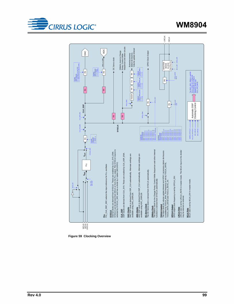
WM8904
Rev 4.0 99
MC
LK
FL
Lf R
EF
f OU
Tf/N
FL
L
FL
L_
CL
K_R
EF
_S
RC
se
lects
th
e in
pu
t re
fere
nce
fo
r F
LL
oscill
ato
r.
SY
SC
LK
Inte
rna
l clo
cks a
re d
erive
d fro
m S
YS
CL
K. T
he
se
are
en
ab
led
by C
LK
_S
YS
_E
NA
.
SY
SC
LK
ca
n b
e d
erive
d fro
m M
CL
K o
r fr
om
th
e F
LL o
utp
ut. T
he
SY
SC
LK
so
urc
e is
se
lecte
d b
y S
YS
CL
K_S
RC
an
d h
as a
div
ide
by 2
op
tio
n (
MC
LK
DIV
).
CL
K_
DS
P
DS
P c
locks a
re d
erive
d fro
m C
LK
_S
YS
. T
he
se
are
en
ab
led
by C
LK
_D
SP
_E
NA
.
DA
C C
loc
ks
DA
C D
SP
clo
ck is d
erive
d fro
m D
SP
_C
LK
au
tom
atica
lly. A
lte
rna
te s
ettin
gs a
re
ava
ilab
le u
sin
g D
AC
_O
SR
12
8.
AD
C C
loc
ks
AD
C D
SP
clo
ck is d
erive
d fro
m D
SP
_C
LK
au
tom
atica
lly. A
lte
rna
te s
ettin
gs a
re
ava
ilab
le u
sin
g A
DC
_O
SR
12
8.
DC
Se
rvo
Clo
ck
Th
e D
C S
erv
o c
lock is d
erive
d fro
m S
YS
CL
K a
uto
ma
tica
lly.
25
6k
Hz C
loc
k
Th
e 2
56
kH
z c
lock fo
r th
e C
ha
rge
Pu
mp
, C
on
tro
l W
rite
Se
qu
en
ce
r a
nd
oth
er
inte
rna
l
fun
ctio
ns is d
erive
d fro
m S
YS
CL
K a
uto
ma
tica
lly
TO
CL
K C
on
tro
l
Th
e s
low
clo
ck fo
r vo
lum
e u
pd
ate
tim
eo
ut a
nd
GP
IO / a
cce
sso
ry d
ete
ct d
e-b
ou
nce
is e
na
ble
d b
y T
OC
LK
_E
NA
. T
he
fre
qu
en
cy is s
et b
y T
OC
LK
_R
AT
E,
TO
CL
K_R
AT
E_
DIV
16
an
d T
OC
LK
_R
AT
E_X
4.
OP
CL
K O
utp
ut
GP
IO o
utp
ut clo
ck fre
qu
en
cy is s
et b
y O
PC
LK
_D
IV.
LR
CL
K R
ate
LR
CL
K r
ate
is s
et b
y L
RC
LK
_R
AT
E in
ma
ste
r m
od
e. T
he
BC
LK
in
pu
t to
th
is d
ivid
er
ma
y b
e in
tern
al o
r e
xte
rna
l.
BC
LK
Ra
te
BC
LK
ra
te is s
et b
y B
CL
K_D
IV in
ma
ste
r m
od
e.
SY
SC
LK
_S
RC
CL
K_
SY
S_
EN
A
FL
L_
CL
K_
RE
F_S
RC
R1
4h[0
]
MC
LK
_D
IV
0 =
MC
LK
1 =
MC
LK
/ 2
CL
K_
DS
P_E
NA C
LK
_D
SP
64
fs o
r 1
28
fsf/N
AD
Cf/N
R0
Ah
[0]
AD
C_O
SR
12
8
0 =
f /
4 (
64
fs)
1 =
f /
2 (
12
8fs
)
DA
Cf/N
Au
tom
atic D
SP
Clo
ckin
g C
on
tro
l
SA
MP
LE
_R
AT
E [
2:0
]
CL
K_S
YS
_R
AT
E [3
:0]
Th
e D
AC
, A
DC
, 2
56
kH
z, a
nd
DC
Se
rvo
clo
cks a
re c
on
fig
ure
d
au
tom
atica
lly a
cco
rdin
g to
SA
MP
LE
_R
AT
E a
nd
CL
K_
SY
S_
RA
TE
.
SY
SC
LK
DA
C_O
SR
12
8
f/N
DC
Se
rvo
clo
ck
GP
IO C
lock O
utp
ut
f/N
OP
CL
K_
DIV
R1
Ah
[11:8
]
OP
CL
K_
DIV
[3:0
]
00
00
= S
YS
CL
K
00
01
= S
YS
CL
K /
2
00
10
= S
YS
CL
K /
3
00
11
= S
YS
CL
K /
4
01
00
= S
YS
CL
K /
5.5
01
01
= S
YS
CL
K /
6
01
10
= S
YS
CL
K /
8
01
11
= S
YS
CL
K /
12
10
00
= S
YS
CL
K /
16
10
01
to
11
11
= R
ese
rve
d
OP
CL
K_
EN
A
f/N
25
6kH
z c
lock to
Ch
arg
e
Pu
mp, C
on
tro
l W
rite
Se
qu
en
ce
r a
nd
oth
er
circu
its
f.N
TO
CL
K_
EN
A
Bu
tto
n/a
cce
sso
ry
de
tect d
e-b
ou
nce
,
Vo
lum
e u
pd
ate
tim
eo
ut
f/N
f/1
02
4
R1
4h
[13
]
TO
CL
K_R
AT
E_X
4
0 =
f x
1
1 =
f x
4
R1
6h
[12]
TO
CL
K_
RA
TE
0 =
f / 2
1 =
f / 1
R1
Ah
[4:0
]
BC
LK
_D
IV[4
:0]
(Ma
ste
r M
od
e)
00
00
0 =
SY
SC
LK
00
00
1 =
SY
SC
LK
/ 1
.5
00
01
0 =
SY
SC
LK
/ 2
00
01
1 =
SY
SC
LK
/ 3
00
10
0 =
SY
SC
LK
/ 4
00
10
1 =
SY
SC
LK
/ 5
00
11
0 =
SY
SC
LK
/ 5
.5
00
11
1 =
SY
SC
LK
/ 6
01
00
0 =
SY
SC
LK
/ 8
01
00
1 =
SY
SC
LK
/ 1
0
01
01
0 =
SY
SC
LK
/ 1
1
01
01
1 =
SY
SC
LK
/ 1
2
01
10
0 =
SY
SC
LK
/ 1
6
01
10
1 =
SY
SC
LK
/ 2
0
01
11
0 =
SY
SC
LK
/ 2
2
BC
LK
_D
IV
[3:0
]
LR
CL
K_
RA
TE
[10:0
]
LR
CL
K
BC
LK
MC
LK
_IN
V
f/N
R1
4h
[14
]
TO
CL
K_R
AT
E_
DIV
16
0 =
f / 1
1 =
f / 1
6
BC
LK
LR
CL
K
AD
C_O
SR
12
8
f/N
R2
1h
[6]
DA
C_
OS
R1
28
0 =
Lo
w p
ow
er
(no
rma
l O
SR
)
1 =
Hig
h p
erf
orm
an
ce
(d
ou
ble
OS
R)
BC
LK
_D
IRL
RC
LK
_D
IR
f/N
MA
ST
ER
MO
DE
CL
OC
K
OU
TP
UT
Sf/N
Figure 59 Clocking Overview

WM8904
100 Rev 4.0
SYSCLK CONTROL
The SYSCLK_SRC bit is used to select the source for SYSCLK. The source may be either the MCLK
input or the FLL output. The MCLK input can be inverted or non-inverted, as selected by the
MCLK_INV bit. The selected source may also be adjusted by the MCLK_DIV divider to generate
SYSCLK. These register fields are described in Table 61. See “Frequency Locked Loop (FLL)” for
more details of the Frequency Locked Loop clock generator.
The SYSCLK signal is enabled by register bit CLK_SYS_ENA. This bit should be set to 0 when
reconfiguring clock sources. It is not recommended to change SYSCLK_SRC while the
CLK_SYS_ENA bit is set.
The following operating frequency limits must be observed when configuring SYSCLK. Failure to
observe these limits will result in degraded noise performance and/or incorrect ADC/DAC functionality.
SYSCLK 3MHz
If DAC_OSR128 = 1 then SYSCLK 6MHz
If DAC_MONO = 1, then SYSCLK 64 x fs
If DAC_MONO = 0, then SYSCLK 128 x fs
If ADCL_ENA = 1 or ADCR_ENA = 1 then SYSCLK 256 x fs
Note that DAC Mono mode (DAC_MONO = 1) is only valid when one or other DAC is disabled. If both
DACs are enabled, then the minimum SYSCLK for clocking the DACs is 128 x fs.
The SYSCLK control register fields are defined in Table 61.
REGISTER
ADDRESS
BIT LABEL DEFAULT DESCRIPTION
R22 (16h)
Clock Rates
2
15 MCLK_INV 0 MCLK Invert
0 = MCLK not inverted
1 = MCLK inverted
14 SYSCLK_SRC 0 SYSCLK Source Select
0 = MCLK
1 = FLL output
2 CLK_SYS_ENA 0 System Clock enable
0 = Disabled
1 = Enabled
R20 (14h)
Clock Rates
0
0 MCLK_DIV 0 Enables divide by 2 on MCLK
0 = SYSCLK = MCLK
1 = SYSCLK = MCLK / 2
Table 61 MCLK and SYSCLK Control
CONTROL INTERFACE CLOCKING
Register map access is possible with or without a Master Clock (MCLK). However, if CLK_SYS_ENA
has been set to 1, then a Master Clock must be present for control register Read/Write operations. If
CLK_SYS_ENA = 1 and MCLK is not present, then register access will be unsuccessful. (Note that
read/write access to register R22, containing CLK_SYS_ENA, is always possible.)
If it cannot be assured that MCLK is present when accessing the register map, then it is required to
set CLK_SYS_ENA = 0 to ensure correct operation.
It is possible to use the WM8904 analogue bypass paths to the differential line outputs (LON/LOP and
RON/ROP) without MCLK. Note that MCLK is always required when using HPOUTL, HPOUTR,
LINEOUTL or LINEOUTR.

WM8904
Rev 4.0 101
CLOCKING CONFIGURATION
The WM8904 supports a wide range of standard audio sample rates from 8kHz to 48kHz. The
Automatic Clocking Configuration simplifies the configuration of the clock dividers in the WM8904 by
deriving most of the necessary parameters from a minimum number of user registers.
The SAMPLE_RATE field selects the sample rate, fs, of the ADC and DAC. Note that the same
sample rate always applies to the ADC and DAC.
The CLK_SYS_RATE field must be set according to the ratio of SYSCLK to fs. When these fields are
set correctly, the Sample Rate Decoder circuit automatically determines the clocking configuration for
all other circuits within the WM8904.
A high performance mode of DAC operation can be selected by setting the DAC_OSR128 bit; in
48kHz sample mode, the DAC_OSR128 feature results in 128x oversampling. Audio performance is
improved, but power consumption is also increased.
REGISTER
ADDRESS
BIT LABEL DEFAULT DESCRIPTION
R33 (21h)
DAC Digital
1
6 DAC_OSR128 0 DAC Oversample Rate Select
0 = Low power (normal OSR)
1 = High performance (double OSR)
R21 (15h)
Clock Rates
1
13:10 CLK_SYS_RAT
E [3:0]
0011 Selects the SYSCLK / fs ratio
0000 = 64
0001 = 128
0010 = 192
0011 = 256
0100 = 384
0101 = 512
0110 = 768
0111 = 1024
1000 = 1408
1001 = 1536
2:0 SAMPLE_RATE
[2:0]
101 Selects the Sample Rate (fs)
000 = 8kHz
001 = 11.025kHz, 12kHz
010 = 16kHz
011 = 22.05kHz, 24kHz
100 = 32kHz
101 = 44.1kHz, 48kHz
110 to 111 = Reserved
Table 62 Automatic Clocking Configuration Control

WM8904
102 Rev 4.0
ADC / DAC CLOCK CONTROL
The clocking of the ADC and DAC circuits is derived from CLK_DSP, which is enabled by
CLK_DSP_ENA. CLK_DSP is generated from SYSCLK which is separately enabled, using the
register bit CLK_SYS_ENA.
Two modes of ADC operation can be selected using the ADC_OSR128 bit; in 48kHz sample mode,
setting the ADC_OSR128 bit results in 128x oversampling. This bit is enabled by default, giving best
audio performance. Deselecting this bit gives 64x oversampling in 48kHz mode, resulting in
decreased power consumption.
Higher performance DAC operation can be achieved by increasing the DAC oversample rate - see
Table 62.
The ADC / DAC Clock Control registers are defined in Table 63.
REGISTER
ADDRESS
BIT LABEL DEFAULT DESCRIPTION
R10 (0Ah)
Analog ADC 0
0 ADC_OSR128 1 ADC Oversampling Ratio
0 = Low Power (64 x fs)
1 = High Performance (128 x fs)
R22 (16h)
Clock Rates 2
1 CLK_DSP_ENA 0 DSP Clock enable
0 = Disabled
1 = Enabled
Table 63 ADC / DAC Clock Control
OPCLK CONTROL
A clock output (OPCLK) derived from SYSCLK may be output on a GPIO pin. This clock is enabled by
register bit OPCLK_ENA, and its frequency is controlled by OPCLK_DIV.
This output of this clock is also dependent upon the GPIO register settings described under “General
Purpose Input/Output (GPIO)”.
REGISTER
ADDRESS
BIT LABEL DEFAULT DESCRIPTION
R22 (16h)
Clock Rates 2
3 OPCLK_ENA 0 GPIO Clock Output Enable
0 = disabled
1 = enabled
R26 (1Ah)
Audio
Interface 2
11:8 OPCLK_DIV [3:0] 0000 GPIO Output Clock Divider
0000 = SYSCLK
0001 = SYSCLK / 2
0010 = SYSCLK / 3
0011 = SYSCLK / 4
0100 = SYSCLK / 5.5
0101 = SYSCLK / 6
0110 = SYSCLK / 8
0111 = SYSCLK / 12
1000 = SYSCLK / 16
1001 to 1111 = Reserved
Table 64 OPCLK Control

WM8904
Rev 4.0 103
TOCLK CONTROL
A slow clock (TOCLK) is derived from the internally generated 256kHz clock to enable input de-
bouncing and volume update timeout functions. This clock is enabled by register bit TOCLK_ENA,
and its frequency is controlled by TOCLK_RATE and TOCLK_RATE_X4, as described in Table 65.
REGISTER
ADDRESS
BIT LABEL DEFAULT DESCRIPTION
R22 (16h)
Clock Rates 2
12 TOCLK_RATE 0 TOCLK Rate Divider (/2)
0 = f / 2
1 = f / 1
0 TOCLK_ENA 0 Zero Cross timeout enable
0 = Disabled
1 = Enabled
R20 (14h)
Clock Rates 0
14 TOCLK_RATE_
DIV16
0 TOCLK Rate Divider (/16)
0 = f / 1
1 = f / 16
13 TOCLK_RATE_
X4
0 TOCLK Rate Multiplier
0 = f x 1
1 = f x 4
Table 65 TOCLK Control
A list of possible TOCLK rates is provided in Table 66.
TOCLK_RATE TOCLK_RATE_X4 TOCLK_RATE_DIV16
TOCLK
FREQ (Hz) PERIOD
(ms)
1 1 0 1000 1
0 1 0 500 2
1 0 0 250 4
0 0 0 125 8
1 1 1 62.5 16
0 1 1 31.25 32
1 0 1 15.625 64
0 0 1 7.8125 128
Table 66 TOCLK Rates
ADC / DAC OPERATION AT 88.2K / 96K
The WM8904 supports ADC or DAC operation at 88.2kHz and 96kHz sample rates. This section
details specific conditions applicable to these operating modes. Note that simultaneous ADC and DAC
operation at 88.2kHz or 96kHz is not possible.
For DAC operation at 88.2kHz or 96kHz sample rates, the available clocking configurations are
detailed in Table 67. DAC operation at these sample rates is achieved by setting the SAMPLE_RATE
field to half the required sample rate (eg. select 48kHz for 96kHz mode).
For DAC operation at 88.2kHz or 96kHz sample rates, the ADCs must both be disabled (ADCL_ENA
= 0 and ADCR_ENA = 0). Also, the DAC_OSR128 register must be set to 0. ReTuneTM Mobile can not
be used during 88.2kHz or 96kHz operation, so EQ_ENA must be set to 0.
The SYSCLK frequency is derived from MCLK. The maximum MCLK frequency is defined in the
“Signal Timing Requirements” section.

WM8904
104 Rev 4.0
SAMPLE RATE REGISTER CONFIGURATION CLOCKING RATIO
88.2kHz SAMPLE_RATE = 101
CLK_SYS_RATE = 0001 (SYSCLK / fs = 128)
BCLK_DIV = 00010
LRCLK_RATE = 040h
SYSCLK = 128 x fs
96kHz SAMPLE_RATE = 101
CLK_SYS_RATE = 0001 (SYSCLK / fs = 128)
BCLK_DIV = 00010
LRCLK_RATE = 040h
SYSCLK = 128 x fs
Table 67 DAC Operation at 88.2kHz and 96kHz Sample Rates
For ADC operation at 88.2kHz or 96kHz sample rates, the available clocking configurations are
detailed in Table 68.
ADC operation at these sample rates is achieved by setting the SAMPLE_RATE field to half the
required sample rate (eg. select 48kHz for 96kHz mode). For ADC operation at 88.2kHz or 96kHz
sample rates, the DACs must both be disabled (DACL_ENA = 0 and DACR_ENA = 0). Note that
ADC_OSR128, ADC_128_OSR_TST_MODE, and ADC_BIASX1P5 must be configured according to
Table 68.
The SYSCLK frequency is derived from MCLK. The maximum MCLK frequency is defined in the
“Signal Timing Requirements” section.
SAMPLE RATE REGISTER CONFIGURATION CLOCKING RATIO
88.2kHz SAMPLE_RATE = 101
CLK_SYS_RATE = 0001 (SYSCLK / fs = 128)
BCLK_DIV = 00010
LRCLK_RATE = 040h
ADC_OSR128 = 0
ADC_128_OSR_TST_MODE = 0
ADC_BIASX1P5 = 0
SYSCLK = 128 x fs
96kHz SAMPLE_RATE = 101
CLK_SYS_RATE = 0001 (SYSCLK / fs = 128)
BCLK_DIV = 00010
LRCLK_RATE = 040h
ADC_OSR128 = 0
ADC_128_OSR_TST_MODE = 0
ADC_BIASX1P5 = 0
SYSCLK = 128 x fs
Table 68 ADC Operation at 88.2kHz and 96kHz Sample Rates
FREQUENCY LOCKED LOOP (FLL)
The integrated FLL can be used to generate SYSCLK from a wide variety of different reference
sources and frequencies. The FLL can use either MCLK, BCLK or LRCLK as its reference, which may
be a high frequency (eg. 12.288MHz) or low frequency (eg. 32,768kHz) reference. The FLL is tolerant
of jitter and may be used to generate a stable SYSCLK from a less stable input signal. The FLL
characteristics are summarised in “Electrical Characteristics”.
Note that the FLL can be used to generate a free-running clock in the absence of an external
reference source. This is described in the “Free-Running FLL Clock” section below.
The FLL is enabled using the FLL_ENA register bit. Note that, when changing FLL settings, it is
recommended that the digital circuit be disabled via FLL_ENA and then re-enabled after the other
register settings have been updated. When changing the input reference frequency FREF, it is
recommended the FLL be reset by setting FLL_ENA to 0.
The FLL_CLK_REF_SRC field allows MCLK, BCLK or LRCLK to be selected as the input reference
clock.

WM8904
Rev 4.0 105
The field FLL_CLK_REF_DIV provides the option to divide the input reference (MCLK, BCLK or
LRCLK) by 1, 2, 4 or 8. This field should be set to bring the reference down to 13.5MHz or below. For
best performance, it is recommended that the highest possible frequency - within the 13.5MHz limit -
should be selected.
The field FLL_CTRL_RATE controls internal functions within the FLL; it is recommended that only the
default setting be used for this parameter. FLL_GAIN controls the internal loop gain and should be set
to the recommended value quoted in Table 71.
The FLL output frequency is directly determined from FLL_FRATIO, FLL_OUTDIV and the real
number represented by FLL_N and FLL_K. The field FLL_N is an integer (LSB = 1); FLL_K is the
fractional portion of the number (MSB = 0.5). The fractional portion is only valid in Fractional Mode
when enabled by the field FLL_FRACN_ENA.
It is recommended that FLL_FRACN_ENA is enabled at all times. Power consumption in the FLL is
reduced in integer mode; however, the performance may also be reduced, with increased noise or
jitter on the output.
If low power consumption is required, then FLL settings must be chosen when N.K is an integer (ie.
FLL_K = 0). In this case, the fractional mode can be disabled by setting FLL_FRACN_ENA = 0.
For best FLL performance, a non-integer value of N.K is required. In this case, the fractional mode
must be enabled by setting FLL_FRACN_ENA = 1. The FLL settings must be adjusted, if necessary,
to produce a non-integer value of N.K.
The FLL output frequency is generated according to the following equation:
FOUT = (FVCO / FLL_OUTDIV)
The FLL operating frequency, FVCO is set according to the following equation:
FVCO = (FREF x N.K x FLL_FRATIO)
See Table 71 for the coding of the FLL_OUTDIV and FLL_FRATIO fields.
FREF is the input frequency, as determined by FLL_CLK_REF_DIV.
FVCO must be in the range 90-100 MHz. Frequencies outside this range cannot be supported.
Note that the output frequencies that do not lie within the ranges quoted above cannot be guaranteed
across the full range of device operating temperatures.
In order to follow the above requirements for FVCO, the value of FLL_OUTDIV should be selected
according to the desired output FOUT. The divider, FLL_OUTDIV, must be set so that FVCO is in the
range 90-100MHz. The available divisions are integers from 4 to 64. Some typical settings of
FLL_OUTDIV are noted in Table 69.
OUTPUT FREQUENCY FOUT FLL_OUTDIV
2.8125 MHz - 3.125 MHz 011111 (divide by 32)
3.75 MHz - 4.1667 MHz 011000 (divide by 24)
5.625 MHz - 6.25 MHz 001111 (divide by 16)
11.25 MHz - 12.5 MHz 000111 (divide by 8)
18 MHz - 20 MHz 000100 (divide by 5)
22.5 MHz - 25 MHz 000011 (divide by 4)
Table 69 Selection of FLL_OUTDIV

WM8904
106 Rev 4.0
The value of FLL_FRATIO should be selected as described in Table 70.
REFERENCE FREQUENCY FREF FLL_FRATIO
1MHz - 13.5MHz 0h (divide by 1)
256kHz - 1MHz 1h (divide by 2)
128kHz - 256kHz 2h (divide by 4)
64kHz - 128kHz 3h (divide by 8)
Less than 64kHz 4h (divide by 16)
Table 70 Selection of FLL_FRATIO
In order to determine the remaining FLL parameters, the FLL operating frequency, FVCO, must be
calculated, as given by the following equation:
FVCO = (FOUT x FLL_OUTDIV)
The value of FLL_N and FLL_K can then be determined as follows:
N.K = FVCO / (FLL_FRATIO x FREF)
See Table 71 for the coding of the FLL_OUTDIV and FLL_FRATIO fields.
Note that FREF is the input frequency, after division by FLL_CLK_REF_DIV, where applicable.
In FLL Fractional Mode, the fractional portion of the N.K multiplier is held in the FLL_K register field.
This field is coded as a fixed point quantity, where the MSB has a weighting of 0.5. Note that, if
desired, the value of this field may be calculated by multiplying K by 216 and treating FLL_K as an
integer value, as illustrated in the following example:
If N.K = 8.192, then K = 0.192
Multiplying K by 216 gives 0.192 x 65536 = 12582.912 (decimal)
Apply rounding to the nearest integer = 12583 (decimal) = 3127 (hex)
For best performance, FLL Fractional Mode should always be used. Therefore, if the calculations yield
an integer value of N.K, then it is recommended to adjust FLL_OUTDIV in order to obtain a non-
integer value of N.K. Care must always be taken to ensure that the FLL operating frequency, FVCO, is
within its recommended limits of 90-100 MHz.
The register fields that control the FLL are described in Table 71. Example settings for a variety of
reference frequencies and output frequencies are shown in Table 73.

WM8904
Rev 4.0 107
REGISTER
ADDRESS
BIT LABEL DEFAULT DESCRIPTION
R116 (74h)
FLL Control 1
2 FLL_FRACN_E
NA
0 FLL Fractional enable
0 = Integer Mode
1 = Fractional Mode
Fractional Mode
(FLL_FRACN_ENA=1) is
recommended in all cases
1 FLL_OSC_ENA 0 FLL Oscillator enable
0 = Disabled
1 = Enabled
FLL_OSC_ENA must be enabled
before enabling FLL_ENA.
Note that this field is required for free-
running FLL modes only.
0 FLL_ENA 0 FLL Enable
0 = Disabled
1 = Enabled
FLL_OSC_ENA must be enabled
before enabling FLL_ENA.
R117 (75h)
FLL Control 2
13:8 FLL_OUTDIV
[5:0]
00_0000 FLL FOUT clock divider
00_0000 = Reserved
00_0001 = Reserved
00_0010 = Reserved
00_0011 = 4
00_0100 = 5
00_0101 = 6
…
11_1110 = 63
11_1111 = 64
(FOUT = FVCO / FLL_OUTDIV)
6:4 FLL_CTRL_RAT
E [2:0]
000 Frequency of the FLL control block
000 = FVCO / 1 (Recommended
value)
001 = FVCO / 2
010 = FVCO / 3
011 = FVCO / 4
100 = FVCO / 5
101 = FVCO / 6
110 = FVCO / 7
111 = FVCO / 8
Recommended that these are not
changed from default.

WM8904
108 Rev 4.0
REGISTER
ADDRESS
BIT LABEL DEFAULT DESCRIPTION
2:0 FLL_FRATIO
[2:0]
111 FVCO clock divider
000 = divide by 1
001 = divide by 2
010 = divide by 4
011 = divide by 8
1XX = divide by 16
000 recommended for FREF > 1MHz
100 recommended for FREF < 64kHz
R118 (76h)
FLL Control 3
15:0 FLL_K [15:0] 0000h Fractional multiply for FREF
(MSB = 0.5)
R119 (77h)
FLL Control 4
14:5 FLL_N [9:0] 177h Integer multiply for FREF
(LSB = 1)
3:0 FLL_GAIN [3:0] 0h Gain applied to error
0000 = x 1 (Recommended value)
0001 = x 2
0010 = x 4
0011 = x 8
0100 = x 16
0101 = x 32
0110 = x 64
0111 = x 128
1000 = x 256
Recommended that these are not
changed from default.
R120 (78h)
FLL Control 5
4:3 FLL_CLK_REF_
DIV [1:0]
00 FLL Clock Reference Divider
00 = MCLK / 1
01 = MCLK / 2
10 = MCLK / 4
11 = MCLK / 8
MCLK (or other input reference) must
be divided down to <=13.5MHz.
For lower power operation, the
reference clock can be divided down
further if desired.
1:0 FLL_CLK_REF_
SRC [1:0]
00 FLL Clock source
00 = MCLK
01 = BCLK
10 = LRCLK
11 = Reserved
Table 71 FLL Register Map

WM8904
Rev 4.0 109
FREE-RUNNING FLL CLOCK
The FLL can generate a clock signal even when no external reference is available. However, it should
be noted that the accuracy of this clock is reduced, and a reference source should always be used
where possible. Note that, in free-running mode, the FLL is not sufficiently accurate for hi-fi ADC or
DAC applications. However, the free-running mode is suitable for clocking most other functions,
including the Write Sequencer, Charge Pump, DC Servo and Class W output driver.
If an accurate reference clock is available at FLL start-up, then the FLL should be configured as
described above. The FLL will continue to generate a stable output clock after the reference input is
stopped or disconnected.
If no reference clock is available at the time of starting up the FLL, then an internal clock frequency of
approximately 12MHz can be generated by enabling the FLL Analogue Oscillator using the
FLL_OSC_ENA register bit, and setting FOUT clock divider to divide by 8 (FLL_OUTDIV = 07h), as
defined in Table 71. Under recommended operating conditions, the FLL output may be forced to
approximately 12MHz by then enabling the FLL_FRC_NCO bit and setting FLL_FRC_NCO_VAL to
19h (see Table 72). The resultant SYSCLK delivers the required clock frequencies for the Class W
output driver, DC Servo, Charge Pump and other functions. Note that the value of
FLL_FRC_NCO_VAL may be adjusted to control FOUT, but care should be taken to maintain the
correct relationship between SYSCLK and the aforementioned functional blocks.
REGISTER
ADDRESS
BIT LABEL DEFAULT DESCRIPTION
R248 (F8h)
FLL NCO Test 1
5:0 FLL_FRC_NCO_
VAL [5:0]
01_1001 FLL Forced oscillator value
Valid range is 000000 to 111111
0x19h (011001) = 12MHz approx
(Note that this field is required for
free-running FLL modes only)
R247 (F7h)
FLL NCO Test 0
0 FLL_FRC_NCO 0 FLL Forced control select
0 = Normal
1 = FLL oscillator controlled by
FLL_FRC_NCO_VAL
(Note that this field is required for
free-running FLL modes only)
Table 72 FLL Free-Running Mode
In both cases described above, the FLL must be selected as the SYSCLK source by setting
SYSCLK_SRC (see Table 61). Note that, in the absence of any reference clock, the FLL output is
subject to a very wide tolerance. See “Electrical Characteristics” for details of the FLL accuracy.
GPIO OUTPUTS FROM FLL
The WM8904 has an internal signal which indicates whether the FLL Lock has been achieved. The
FLL Lock status is an input to the Interrupt control circuit and can be used to trigger an Interrupt event
- see “Interrupts”.
The FLL Lock signal can be output directly on a GPIO pin as an external indication of FLL Lock. See
“General Purpose Input/Output (GPIO)” for details of how to configure a GPIO pin to output the FLL
Lock signal.
The FLL Clock can be output directly on a GPIO pin as a clock signal for other circuits. Note that the
FLL Clock may be output even if the FLL is not selected as the WM8904 SYSCLK source. The
clocking configuration is illustrated in Figure 59. See “General Purpose Input/Output (GPIO)” for
details of how to configure a GPIO pin to output the FLL Clock.

WM8904
110 Rev 4.0
EXAMPLE FLL CALCULATION
To generate 12.288 MHz output (FOUT) from a 12.000 MHz reference clock (FREF):
Set FLL_CLK_REF_DIV in order to generate FREF <=13.5MHz:
FLL_CLK_REF_DIV = 00 (divide by 1)
Set FLL_CTRL_RATE to the recommended setting:
FLL_CTRL_RATE = 000 (divide by 1)
Set FLL_GAIN to the recommended setting:
FLL_GAIN = 0000 (multiply by 1)
Set FLL_OUTDIV for the required output frequency as shown in Table 69:-
FOUT = 12.288 MHz, therefore FLL_OUTDIV = 07h (divide by 8)
Set FLL_FRATIO for the given reference frequency as shown in Table 70:
FREF = 12MHz, therefore FLL_FRATIO = 0h (divide by 1)
Calculate FVCO as given by FVCO = FOUT x FLL_OUTDIV:-
FVCO = 12.288 x 8 = 98.304MHz
Calculate N.K as given by N.K = FVCO / (FLL_FRATIO x FREF):
N.K = 98.304 / (1 x 12) = 8.192
Determine FLL_N and FLL_K from the integer and fractional portions of N.K:-
FLL_N is 8. FLL_K is 0.192
Confirm that N.K is a fractional quantity and set FLL_FRACN_ENA:
N.K is fractional. Set FLL_FRACN_ENA = 1.
Note that, if N.K is an integer, then an alternative value of FLL_FRATIO should be selected in order
to produce a fractional value of N.K.

WM8904
Rev 4.0 111
EXAMPLE FLL SETTINGS
Table 73 provides example FLL settings for generating common SYSCLK frequencies from a variety
of low and high frequency reference inputs.
FREF FOUT FLL_CLK_
REF_DIV
FVCO FLL_N FLL_K FLL_
FRATIO
FLL_
OUTDIV
FLL_
FRACN
_ENA
32.768 kHz 12.288 MHz Divide by 1
(0h)
98.304
MHz
187
(0BBh)
0.5
(8000h)
16
(4h)
8
(7h)
1
32.768 kHz 11.288576
MHz
Divide by 1
(0h)
90.308608
MHz
344
(158h)
0.5
(8000h)
8
(3h)
8
(7h)
1
32.768 kHz 11.2896
MHz
Divide by 1
(0h)
90.3168
MHz
344
(158h)
0.53125
(8800h)
8
(3h)
8
(7h)
1
48 kHz 12.288 MHz Divide by 1
(0h)
98.304
MHz
256
(100h)
0
(0000h)
8
(3h)
8
(7h)
0
12.000 MHz 12.288 MHz Divide by 1
(0h)
98.3040
MHz
8
(008h)
0.192
(3127h)
1
(0h)
8
(7h)
1
12.000 MHz 11.289597
MHz
Divide by 1
(0h)
90.3168
MHz
7
(007h)
0.526398
(86C2h)
1
(0h)
8
(7h)
1
12.288 MHz 12.288 MHz Divide by 1
(0h)
98.304
MHz
8
(008h)
0
(0000h)
1
(0h)
8
(7h)
0
12.288 MHz 11.2896
MHz
Divide by 1
(0h)
90.3168
MHz
7
(007h)
0.35
(599Ah)
1
(0h)
8
(7h)
1
13.000 MHz 12.287990
MHz
Divide by 1
(0h)
98.3040
MHz
7
(007h)
0.56184
(8FD5h)
1
(0h)
8
(7h)
1
13.000 MHz 11.289606
MHz
Divide by 1
(0h)
90.3168
MHz
6
(006h)
0.94745
(F28Ch)
1
(0h)
8
(7h)
1
19.200 MHz 12.287988
MHz
Divide by 2
(1h)
98.3039
MHz
5
(005h)
0.119995
(1EB8h)
1
(0h)
8
(7h)
1
19.200 MHz 11.289588
MHz
Divide by 2
(1h)
90.3168
MHz
4
(004h)
0.703995
(B439h)
1
(0h)
8
(7h)
1
Table 73 Example FLL Settings

WM8904
112 Rev 4.0
GENERAL PURPOSE INPUT/OUTPUT (GPIO)
The WM8904 provides four multifunction pins that can be configured to provide a number of different
functions. These are digital input/output pins on the DBVDD power domain. The GPIO pins are:
IRQ/GPIO1
GPIO2
GPIO3
BCLK/GPIO4
Each general purpose I/O pin can be configured to be a GPIO input or configured as one of a number
of output functions. Signal de-bouncing can be selected on GPIO input pins for use with jack/button
detect applications. Table 74 lists the functions that are available on each of the GPIO pins.
GPIO Pin Function
GPIO PINS
IRQ / GPIO1 GPIO2 GPIO3 BCLK / GPIO4
GPIO input
(including jack/button detect)
Yes Yes Yes Yes
GPIO output Yes Yes Yes Yes
BCLK No No No Yes
Interrupt (IRQ) Yes Yes Yes Yes
MICBIAS current detect Yes Yes Yes Yes
MICBIAS short-circuit detect Yes Yes Yes Yes
Digital microphone interface
(DMIC clock output)
Yes Yes Yes Yes
FLL Lock output Yes Yes Yes Yes
FLL Clock output Yes Yes Yes Yes
Table 74 GPIO Functions Available
IRQ/GPIO1
The IRQ/GPIO1 pin is configured using the register bits described in Table 75. By default, this pin is
IRQ output with pull-down resistor enabled.
REGISTER
ADDRESS
BIT LABEL DEFAULT DESCRIPTION
R121 (79h)
GPIO
Control 1
5 GPIO1_PU 0 GPIO1 pull-up resistor enable
0 = pull-up disabled
1 = pull-up enabled
4 GPIO1_PD 1 GPIO1 pull-down resistor enable
0 = pull-down disabled
1 = pull-down enabled
3:0 GPIO1_SEL [3:0] 0100 GPIO1 Function Select
0000 = Input pin
0001 = Clock output
(f=SYSCLK/OPCLKDIV)
0010 = Logic '0'
0011 = Logic '1'
0100 = IRQ (default)
0101 = FLL Lock
0110 = Mic Detect
0111 = Mic Short
1000 = DMIC clock out
1001 = FLL Clock Output
1010 to 1111 = Reserved
Table 75 IRQ/GPIO1 Control

WM8904
Rev 4.0 113
GPIO2
The GPIO2 pin is configured using the register bits described in Table 76. By default, this pin is GPIO
input with pull-down resistor enabled.
REGISTER
ADDRESS
BIT LABEL DEFAULT DESCRIPTION
R122 (7Ah)
GPIO
Control 2
5 GPIO2_PU 0 GPIO2 pull-up resistor enable
0 = pull-up disabled
1 = pull-up enabled
4 GPIO2_PD 1 GPIO2 pull-down resistor enable
0 = pull-down disabled
1 = pull-down enabled
3:0 GPIO2_SEL [3:0] 0000 GPIO2 Function Select
0000 = Input pin (default)
0001 = Clock output
(f=SYSCLK/OPCLKDIV)
0010 = Logic '0'
0011 = Logic '1'
0100 = IRQ
0101 = FLL Lock
0110 = Mic Detect
0111 = Mic Short
1000 = DMIC clock out
1001 = FLL Clock Output
1010 to 1111 = Reserved
Table 76 GPIO2 Control
GPIO3
The GPIO3 pin is configured using the register bits described in Table 77. By default, this pin is GPIO
input with pull-down resistor enabled.
REGISTER
ADDRESS
BIT LABEL DEFAULT DESCRIPTION
R123 (7Bh)
GPIO
Control 3
5 GPIO3_PU 0 GPIO3 pull-up resistor enable
0 = pull-up disabled
1 = pull-up enabled
4 GPIO3_PD 1 GPIO3 pull-down resistor enable
0 = pull-down disabled
1 = pull-down enabled
3:0 GPIO3_SEL [3:0] 0000 GPIO3 Function Select
0000 = Input pin (default)
0001 = Clock output
(f=SYSCLK/OPCLKDIV)
0010 = Logic '0'
0011 = Logic '1'
0100 = IRQ
0101 = FLL Lock
0110 = Mic Detect
0111 = Mic Short
1000 = DMIC clock out
1001 = FLL Clock Output
1010 to 1111 = Reserved
Table 77 GPIO3 Control

WM8904
114 Rev 4.0
BCLK/GPIO4
The BCLK/GPIO4 pin is configured using the register bits described in Table 78. By default, this pin
provides the BCLK function associated with the Digital Audio Interface. The BCLK function can
operate in slave mode (BCLK input) or in master mode (BCLK output), depending on the BCLK_DIR
register bit as described in the “Digital Audio Interface” section.
It is possible to configure the BCLK/GPIO4 pin to provide various GPIO functions; in this case, the
BCLK function is provided using the MCLK pin. Note that the BCLK function is always in slave mode
(BCLK input) in this mode.
To select the GPIO4 functions, it is required to set BCLK_DIR = 0 (see Table 56) and to set
GPIO_BCLK_MODE_ENA = 1 (see Table 78 below). In this configuration, the MCLK input is used as
the bit-clock (BCLK) for the Digital Audio Interface.
When the BCLK/GPIO4 pin is configured as GPIO4, then the pin function is determined by the
GPIO_BCLK_SEL register field.
REGISTER
ADDRESS
BIT LABEL DEFAULT DESCRIPTION
R124 (7Ch)
GPIO
Control 4
7 GPIO_BCLK_MODE_
ENA
0 Selects BCLK/GPIO4 pin function
0 = BCLK/GPIO4 is used as BCLK
1 = BCLK/GPIO4 is used as GPIO.
MCLK provides the BCLK in the AIF
in this mode.
3:0 GPIO_BCLK_SEL
[3:0]
0000 GPIO_BCLK function select:
0000 = Input Pin (default)
0001 = Clock output
(f=SYSCLK/OPCLKDIV)
0010 = Logic '0'
0011 = Logic '1'
0100 = IRQ
0101 = FLL Lock
0110 = Mic Detect
0111 = Mic Short
1000 = DMIC clock out
1001 = FLL Clock Output
1010 to 1111 = Reserved
Table 78 BCLK/GPIO4 Control

WM8904
Rev 4.0 115
INTERRUPTS
The Interrupt Controller has multiple inputs; these include the GPIO input pins and the MICBIAS
current detection circuits. Any combination of these inputs can be used to trigger an Interrupt (IRQ)
event.
WM8904 interrupt events may be triggered in response to external GPIO inputs, FLL Lock status,
MICBIAS status or Write Sequencer status. Note that the GPIO inputs (including GPI7 and GPI8) are
only supported as interrupt events when the respective pin is configured as a GPIO input.
There is an Interrupt Status field associated with each of the IRQ inputs. These are contained in the
Interrupt Status Register (R127), as described in Table 79. The status of the IRQ inputs can be read
from this register at any time, or in response to the Interrupt Output being signalled via a GPIO pin.
Individual mask bits can select or deselect different functions from the Interrupt controller. These are
listed within the Interrupt Status Mask register (R128), as described in Table 80. Note that the
Interrupt Status fields remain valid, even when masked, but the masked bits will not cause the
Interrupt (IRQ) output to be asserted.
The Interrupt (IRQ) output represents the logical ‘OR’ of all unmasked IRQ inputs. The bits within the
Interrupt Status register (R127) are latching fields and, once set, are not reset until a ‘1’ is written to
the respective register bit in the Interrupt Status Register. The Interrupt (IRQ) output is not reset until
each of the unmasked IRQ inputs has been reset.
Each of the IRQ inputs can be individually inverted in the Interrupt function, enabling either active high
or active low behaviour on each IRQ input. The polarity inversion is controlled using the bits contained
in the Interrupt Polarity register (R129).
Each of the IRQ inputs can be debounced to ensure that spikes and transient glitches do not assert
the Interrupt Output. This is selected using the bits contained in the Interrupt Debounce Register
(R130).
The WM8904 Interrupt Controller circuit is illustrated in Figure 60. The associated control fields are
described in Table 79 through to Table 82.
GPIO4
WSEQ Busy Status
GPIO_BCLK_EINT_POL
WSEQ_EINT_POL
IM_GPIO_BCLK_EINT
GPIO3
GPIO2
GPIO3_EINT_POL
GPIO2_EINT_POL
GPIO_BCLK_EINT_DB
WSEQ_EINT_DB
GPIO3_EINT_DB
GPIO2_EINT_DB
GPIO_BCLK_EINT
WSEQ_EINT
GPIO3_EINT
GPIO2_EINT
IM_WSEQ_EINT
IM_GPIO3_EINT
IM_GPIO2_EINT
IRQ
GPIO1
GPI8
GPIO1_EINT_POL
GPI8_EINT_POL
IM_GPIO1_EINT
GPI7
FLL Lock
GPI7_EINT_POL
FLL_LOCK_EINT_POL
GPIO1_EINT_DB
GPI8_EINT_DB
GPI7_EINT_DB
FLL_LOCK_EINT_DB
GPIO1_EINT
GPI8_EINT
GPI7_EINT
FLL_LOCK_EINT
IM_GPI8_EINT
IM_GPI7_EINT
IM_FLL_LOCK_EINT
Mic Detect
MIC_SHRT_EINT_POL
MIC_DET_EINT_POL
MIC_SHRT_EINT_DB
MIC_DET_EINT_DB
MIC_SHRT_EINT
MIC_DET_EINT
IM_MIC_SHRT_EINT
IM_MIC_DET_EINT
Input De-
Bounce
Status
Register
Latches
Cleared
when a ‘1’
is written
Mic Short Circuit
Figure 60 Interrupt Controller

WM8904
116 Rev 4.0
REGISTER
ADDRESS
BIT LABEL DEFAULT DESCRIPTION
R127 (7Fh)
Interrupt
Status
10 IRQ 0 Logical OR of all other interrupt
flags
9 GPIO_BCLK_EINT 0 GPIO4 interrupt
0 = interrupt not set
1 = interrupt is set
Cleared when a ‘1’ is written
8 WSEQ_EINT 0 Write Sequence interrupt
0 = interrupt not set
1 = interrupt is set
Cleared when a ‘1’ is written.
Note that the read value of
WSEQ_EINT is not valid whilst the
Write Sequencer is Busy
7 GPIO3_EINT 0 GPIO3 interrupt
0 = interrupt not set
1 = interrupt is set
Cleared when a ‘1’ is written
6 GPIO2_EINT 0 GPIO2 interrupt
0 = interrupt not set
1 = interrupt is set
Cleared when a ‘1’ is written
5 GPIO1_EINT 0 GPIO1 interrupt
0 = interrupt not set
1 = interrupt is set
Cleared when a ‘1’ is written
4 GPI8_EINT 0 GPI8 interrupt
0 = interrupt not set
1 = interrupt is set
Cleared when a ‘1’ is written
3 GPI7_EINT 0 GPI7 interrupt
0 = interrupt not set
1 = interrupt is set
Cleared when a ‘1’ is written
2 FLL_LOCK_EINT 0 FLL Lock interrupt
0 = interrupt not set
1 = interrupt is set
Cleared when a ‘1’ is written
1 MIC_SHRT_EINT 0 MICBIAS short circuit interrupt
0 = interrupt not set
1 = interrupt is set
Cleared when a ‘1’ is written
0 MIC_DET_EINT 0 MICBIAS current detect interrupt
0 = interrupt not set
1 = interrupt is set
Cleared when a ‘1’ is written
Table 79 Interrupt Status Registers

WM8904
Rev 4.0 117
REGISTER
ADDRESS
BIT LABEL DEFAULT DESCRIPTION
R128 (80h)
Interrupt
Status Mask
9 IM_GPIO_BCLK_EINT 1 GPIO4 interrupt mask
0 = do not mask interrupt
1 = mask interrupt
8 IM_WSEQ_EINT 1 Write sequencer interrupt
mask
0 = do not mask interrupt
1 = mask interrupt
7 IM_GPIO3_EINT 1 GPIO3 interrupt mask
0 = do not mask interrupt
1 = mask interrupt
6 IM_GPIO2_EINT 1 GPIO2 interrupt mask
0 = do not mask interrupt
1 = mask interrupt
5 IM_GPIO1_EINT 1 GPIO1 interrupt mask
0 = do not mask interrupt
1 = mask interrupt
4 IM_GPI8_EINT 1 GPI8 interrupt mask
0 = do not mask interrupt
1 = mask interrupt
3 IM_GPI7_EINT 1 GPI7 interrupt mask
0 = do not mask interrupt
1 = mask interrupt
2 IM_FLL_LOCK_EINT 1 FLL Lock interrupt mask
0 = do not mask interrupt
1 = mask interrupt
1 IM_MIC_SHRT_EINT 1 MICBIAS short circuit interrupt
mask
0 = do not mask interrupt
1 = mask interrupt
0 IM_MIC_DET_EINT 1 MICBIAS current detect
interrupt mask
0 = do not mask interrupt
1 = mask interrupt
Table 80 Interrupt Mask Registers
REGISTER
ADDRESS
BIT LABEL DEFAULT DESCRIPTION
R129 (81h)
Interrupt
Polarity
9 GPIO_BCLK_EINT_POL 0 GPIO4 interrupt polarity
0 = active high
1 = active low
8 WSEQ_EINT_POL 0 Write Sequencer interrupt
polarity
0 = active high (interrupt is
triggered when WSEQ is
busy)
1 = active low (interrupt is
triggered when WSEQ is idle)
7 GPIO3_EINT_POL 0 GPIO3 interrupt polarity
0 = active high
1 = active low
6 GPIO2_EINT_POL 0 GPIO2 interrupt polarity
0 = active high
1 = active low

WM8904
118 Rev 4.0
REGISTER
ADDRESS
BIT LABEL DEFAULT DESCRIPTION
5 GPIO1_EINT_POL 0 GPIO1 interrupt polarity
0 = active high
1 = active low
4 GPI8_EINT_POL 0 GPI8 interrupt polarity
0 = active high
1 = active low
3 GPI7_EINT_POL 0 GPI7 interrupt polarity
0 = active high
1 = active low
2 FLL_LOCK_EINT_POL 0 FLL Lock interrupt polarity
0 = active high (interrupt is
triggered when FLL Lock is
reached)
1 = active low (interrupt is
triggered when FLL is not
locked)
1 MIC_SHRT_EINT_POL 0 MICBIAS short circuit interrupt
polarity
0 = active high
1 = active low
0 MIC_DET_EINT_POL 0 MICBIAS current detect
interrupt polarity
0 = active high
1 = active low
Table 81 Interrupt Polarity Registers
REGISTER
ADDRESS
BIT LABEL DEFAULT DESCRIPTION
R130 (82h)
Interrupt
Debounce
9 GPIO_BCLK_EINT_DB 0 GPIO4 interrupt debounce
0 = disabled
1 = enabled
8 WSEQ_EINT_DB 0 Write Sequencer interrupt
debounce enable
0 = disabled
1 = enabled
7 GPIO3_EINT_DB 0 GPIO3 input debounce
0 = disabled
1 = enabled
6 GPIO2_EINT_DB 0 GPIO2 input debounce
0 = disabled
1 = enabled
5 GPIO1_EINT_DB 0 GPIO1 input debounce
0 = disabled
1 = enabled
4 GPI8_EINT_DB 0 GPI8 input debounce
0 = disabled
1 = enabled
3 GPI7_EINT_DB 0 GPI7 input debounce
0 = disabled
1 = enabled
2 FLL_LOCK_EINT_DB 0 FLL Lock debounce
0 = disabled
1 = enabled

WM8904
Rev 4.0 119
REGISTER
ADDRESS
BIT LABEL DEFAULT DESCRIPTION
1 MIC_SHRT_EINT_DB 0 MICBIAS short circuit interrupt
debounce
0 = disabled
1 = enabled
0 MIC_DET_EINT_DB 0 MICBIAS current detect
interrupt debounce
0 = disabled
1 = enabled
Table 82 Interrupt Debounce Registers
USING IN1L AND IN1R AS INTERRUPT INPUTS
IN1L pin has three input functions.
Analogue audio input
Digital microphone input (DMICDAT1)
Digital interrupt input (GPI7)
IN1R pin has three input functions.
Analogue audio input
Digital microphone input (DMICDAT2)
Digital interrupt input (GPI8)
To use these pins as digital interrupt inputs, they must be enabled using the GPI7_ENA and
GPI8_ENA bits as described in Table 83.
REGISTER
ADDRESS
BIT LABEL DEFAULT DESCRIPTION
R124 (7Ch)
GPIO Control 4
9 GPI7_ENA 0 GPI7 input enable
0 = disabled
1 = enabled
8 GPI8_ENA 0 GPI8 input enable
0 = disabled
1 = enabled
Table 83 Enabling IN1L and IN1R as Interrupts GPI7 and GPI8

WM8904
120 Rev 4.0
CONTROL INTERFACE
The WM8904 is controlled by writing to registers through a 2-wire serial control interface. Readback is
available for all registers, including Chip ID, power management status and GPIO status.
Note that, if it cannot be assured that MCLK is present when accessing the register map, then it is
required to set CLK_SYS_ENA = 0 to ensure correct operation. See “Clocking and Sample Rates” for
details of CLK_SYS_ENA.
The WM8904 is a slave device on the control interface; SCLK is a clock input, while SDA is a bi-
directional data pin. To allow arbitration of multiple slaves (and/or multiple masters) on the same
interface, the WM8904 transmits logic 1 by tri-stating the SDA pin, rather than pulling it high. An
external pull-up resistor is required to pull the SDA line high so that the logic 1 can be recognised by
the master.
In order to allow many devices to share a single 2-wire control bus, every device on the bus has a
unique 8-bit device ID (this is not the same as the 8-bit address of each register in the WM8904). The
WM8904 device ID is 0011 0100 (34h). The LSB of the device ID is the Read/Write bit; this bit is set to
logic 1 for “Read” and logic 0 for “Write”.
The WM8904 operates as a slave device only. The controller indicates the start of data transfer with a
high to low transition on SDA while SCLK remains high. This indicates that a device ID, register
address and data will follow. The WM8904 responds to the start condition and shifts in the next eight
bits on SDA (8-bit device ID including Read/Write bit, MSB first). If the device ID received matches the
device ID of the WM8904, then the WM8904 responds by pulling SDA low on the next clock pulse
(ACK). If the device ID is not recognised or the R/W bit is ‘1’ when operating in write only mode, the
WM8904 returns to the idle condition and waits for a new start condition and valid address.
If the device ID matches the device ID of the WM8904, the data transfer continues as described
below. The controller indicates the end of data transfer with a low to high transition on SDA while
SCLK remains high. After receiving a complete address and data sequence the WM8904 returns to
the idle state and waits for another start condition. If a start or stop condition is detected out of
sequence at any point during data transfer (i.e. SDA changes while SCLK is high), the device returns
to the idle condition.
The WM8904 supports the following read and write operations:
Single write
Single read
Multiple write using auto-increment
Multiple read using auto-increment
The sequence of signals associated with a single register write operation is illustrated in Figure 61.
A1D7 D1 A7SDA
SCLK
device ID data bits B15 – B8
A0 B15 B8 B1 B0
Note: The SDA pin is used as input for the control register address and data; SDA is
pulled low by the receiving device to provide the acknowledge (ACK) response
R/W B9 B7
register address data bits B7 – B0START (Write) ACK ACK ACK STOPACK
Figure 61 Control Interface Register Write
The sequence of signals associated with a single register read operation is illustrated in Figure 62.

WM8904
Rev 4.0 121
A1D7 D1 A7SDA
SCLK
device ID device ID
A0 D6 B9 B8
Note: The SDA pin is driven by both the master and slave devices in turn to transfer device address, register address, data and ACK responses
R/W D0 B15
register address data bits B15 – B8START (Write) ACK ACK ACK
R/W
(Read)
B1 B0B7
data bits B15 – B8ACK STOPACKRptSTART
Figure 62 Control Interface Register Read
The Control Interface also supports other register operations, as listed above. The interface protocol
for these operations is summarised below. The terminology used in the following figures is detailed in
Table 84.
Note that multiple write and multiple read operations are supported using the auto-increment mode.
This feature enables the host processor to access sequential blocks of the data in the WM8904
register map faster than is possible with single register operations.
TERMINOLOGY DESCRIPTION
S Start Condition
Sr Repeated start
A Acknowledge (SDA Low)
A Not Acknowledge (SDA High)
P Stop Condition
R/W ReadNotWrite 0 = Write
1 = Read
[White field] Data flow from bus master to WM8904
[Grey field] Data flow from WM8904 to bus master
Table 84 Control Interface Terminology
S A Register Address
(0)
A MSByte Data A LSByte Data A P
8 bits 8 bits 8 bits 8 bits
Device ID RW
Figure 63 Single Register Write to Specified Address
Sr A PMSByte Data
(1)
LSByte DataAS A Register Address
(0)
A ADevice ID RW Device ID RW
Figure 64 Single Register Read from Specified Address
S A Register Address
(0)
A MSByte Data 0 A LSByte Data 0 A
Written to 'Register Address'
A MSByte Data N A LSByte Data N A P
Written to 'Register Address+N'
MSByte Data 1
MSByte Data N-2 A MSByte Data N-1 A LSByte Data N-1
Written to 'Register Address+N-1'
Device ID RW
Figure 65 Multiple Register Write to Specified Address using Auto-increment

WM8904
122 Rev 4.0
SrS A Register Address
(0)
A A
(1)
Read from 'Register Address'
MSByte Data 0 LSByte Data 0A A
PMSByte Data N LSByte Data NA AAMSByte Data N-1 LSByte Data N-1AA
Read from 'Last Register Address+N'Read from 'Last Register Address+N-1'
Device ID RW Device ID RW
Figure 66 Multiple Register Read from Specified Address using Auto-increment
A
PMSByte Data N
(1)
LSByte Data NA
S
AA
MSByte Data 0 LSByte Data 0A A
MSByte Data N-1 LSByte Data N-1AA
Read from 'Last Register Address'
Read from 'Last Register Address+N'Read from 'Last Register Address+N-1'
MSByte Data 1 LSByte Data 1A A
Read from 'Last Register Address+1'
Device ID RW
Figure 67 Multiple Register Read from Last Address using Auto-increment
CONTROL WRITE SEQUENCER
The Control Write Sequencer is a programmable unit that forms part of the WM8904 control interface
logic. It provides the ability to perform a sequence of register write operations with the minimum of
demands on the host processor - the sequence may be initiated by a single operation from the host
processor and then left to execute independently.
Default sequences for Start-Up and Shutdown are provided (see “Default Sequences” section). It is
recommended that these default sequences are used unless changes become necessary.
When a sequence is initiated, the sequencer performs a series of pre-defined register writes. The host
processor informs the sequencer of the start index of the required sequence within the sequencer’s
memory. At each step of the sequence, the contents of the selected register fields are read from the
sequencer’s memory and copied into the WM8904 control registers. This continues sequentially
through the sequencer’s memory until an “End of Sequence” bit is encountered; at this point, the
sequencer stops and an Interrupt status flag is asserted. For cases where the timing of the write
sequence is important, a programmable delay can be set for specific steps within the sequence.
Note that the Control Write Sequencer’s internal clock is derived from the internal clock SYSCLK. An
external MCLK signal must be present when using the Control Write Sequencer, and SYSCLK must
be enabled by setting CLK_SYS_ENA (see “Clocking and Sample Rates”). The clock division from
MCLK is handled transparently by the WM8904 without user intervention, as long as MCLK and
sample rates are set correctly.
INITIATING A SEQUENCE
The Register fields associated with running the Control Write Sequencer are described in Table 85.
The Write Sequencer Clock is enabled by setting the WSEQ_ENA bit. Note that the operation of the
Control Write Sequencer also requires the internal clock SYSCLK to be enabled via the
CLK_SYS_ENA (see “Clocking and Sample Rates”).
The start index of the required sequence must be written to the WSEQ_START_INDEX field. Setting
the WSEQ_START bit initiates the sequencer at the given start index.
The Write Sequencer can be interrupted by writing a logic 1 to the WSEQ_ABORT bit.

WM8904
Rev 4.0 123
The current status of the Write Sequencer can be read using two further register fields - when the
WSEQ_BUSY bit is asserted, this indicates that the Write Sequencer is busy. Note that, whilst the
Control Write Sequencer is running a sequence (indicated by the WSEQ_BUSY bit), normal read/write
operations to the Control Registers cannot be supported. (The Write Sequencer registers and the
Software Reset register can still be accessed when the Sequencer is busy.) The index of the current
step in the Write Sequencer can be read from the WSEQ_CURRENT_INDEX field; this is an indicator
of the sequencer’s progress. On completion of a sequence, this field holds the index of the last step
within the last commanded sequence.
When the Write Sequencer reaches the end of a sequence, it asserts the WSEQ_EINT flag in
Register R127 (see Table 79 within the “Interrupts” section). This flag can be used to generate an
Interrupt Event on completion of the sequence. Note that the WSEQ_EINT flag is asserted to indicate
that the WSEQ is NOT Busy.
REGISTER
ADDRESS
BIT LABEL DEFAULT DESCRIPTION
R108 (6Ch)
Write
Sequencer 0
8 WSEQ_ENA 0 Write Sequencer Enable.
0 = Disabled
1 = Enabled
R111 (6Fh)
Write
Sequencer 3
9 WSEQ_ABORT 0 Writing a 1 to this bit aborts the
current sequence and returns
control of the device back to the
serial control interface.
8 WSEQ_START 0 Writing a 1 to this bit starts the write
sequencer at the memory location
indicated by the
WSEQ_START_INDEX field. The
sequence continues until it reaches
an “End of sequence” flag. At the
end of the sequence, this bit will be
reset by the Write Sequencer.
5:0 WSEQ_START_
INDEX [5:0]
00_0000 Sequence Start Index. This is the
memory location of the first
command in the selected sequence.
0 to 31 = RAM addresses
32 to 48 = ROM addresses
49 to 63 = Reserved
R112 (70h)
Write
Sequencer 4
9:4 WSEQ_CURRE
NT_INDEX [5:0]
00_0000 Sequence Current Index (read only):
This is the location of the most
recently accessed command in the
write sequencer memory.
0 WSEQ_BUSY 0 Sequencer Busy flag (read only):
0 = Sequencer idle
1 = Sequencer busy
Note: it is not possible to write to
control registers via the control
interface while the Sequencer is
Busy.
Table 85 Write Sequencer Control - Initiating a Sequence
PROGRAMMING A SEQUENCE
A sequence consists of write operations to data bits (or groups of bits) within the control registers. The
register fields associated with programming the Control Write Sequencer are described in Table 86.
For each step of the sequence being programmed, the Sequencer Index must be written to the
WSEQ_WRITE_INDEX field. The values 0 to 31 correspond to all the available RAM addresses within
the Write Sequencer memory. (Note that memory addresses 32 to 48 also exist, but these are ROM
addresses, which are not programmable.)
Having set the Index as described above, Register R109 must be written to (containing the Control
Register Address, the Start Bit Position and the Field Width applicable to this step of the sequence).

WM8904
124 Rev 4.0
Also, Register R110 must be written to (containing the Register Data, the End of Sequence flag and
the Delay time required after this step is executed). After writing to these two registers, the next step in
the sequence may be programmed by updating WSEQ_WRITE_INDEX and repeating the procedure.
WSEQ_ADDR is an 8-bit field containing the Control Register Address in which the data should be
written.
WSEQ_DATA_START is a 4-bit field which identifies the LSB position within the selected Control
Register to which the data should be written. Setting WSEQ_DATA_START = 0100 will cause 1-bit
data to be written to bit 4. With this setting, 4-bit data would be written to bits 7:4 and so on.
WSEQ_DATA_WIDTH is a 3-bit field which identifies the width of the data block to be written. This
enables selected portions of a Control Register to be updated without any concern for other bits within
the same register, eliminating the need for read-modify-write procedures. Values of 0 to 7 correspond
to data widths of 1 to 8 respectively. For example, setting WSEQ_DATA_WIDTH = 010 will cause a
3-bit data block to be written. Note that the maximum value of this field corresponds to an 8-bit data
block; writing to register fields greater than 8 bits wide must be performed using two separate
operations of the Control Write Sequencer.
WSEQ_DATA is an 8-bit field which contains the data to be written to the selected Control Register.
The WSEQ_DATA_WIDTH field determines how many of these bits are written to the selected
register; the most significant bits (above the number indicated by WSEQ_DATA_WIDTH) are ignored.
WSEQ_DELAY is a 4-bit field which controls the waiting time between the current step and the next
step in the sequence. The total delay time per step (including execution) is given by:
T = k × (2 WSEQ_DELAY + 8)
where k = 62.5s (under recommended operating conditions)
This gives a useful range of execution/delay times from 562s up to 2.048s per step.
WSEQ_EOS is a 1-bit field which indicates the End of Sequence. If this bit is set, then the Control
Write Sequencer will automatically stop after this step has been executed.
REGISTER
ADDRESS
BIT LABEL DEFAULT DESCRIPTION
R108 (6Ch)
Write
Sequencer
0
4:0 WSEQ_WRITE
_INDEX [4:0]
0_0000 Sequence Write Index. This is the
memory location to which any updates
to R109 and R110 will be copied.
0 to 31 = RAM addresses
R109 (6Dh)
Write
Sequencer
1
14:12 WSEQ_DATA_
WIDTH [2:0]
000 Width of the data block written in this
sequence step.
000 = 1 bit
001 = 2 bits
010 = 3 bits
011 = 4 bits
100 = 5 bits
101 = 6 bits
110 = 7 bits
111 = 8 bits
11:8 WSEQ_DATA_
START [3:0]
0000 Bit position of the LSB of the data
block written in this sequence step.
0000 = Bit 0
…
1111 = Bit 15
7:0 WSEQ_ADDR
[7:0]
0000_0000 Control Register Address to be written
to in this sequence step.

WM8904
Rev 4.0 125
REGISTER
ADDRESS
BIT LABEL DEFAULT DESCRIPTION
R110 (6Eh)
Write
Sequencer
2
14 WSEQ_EOS 0 End of Sequence flag. This bit
indicates whether the Control Write
Sequencer should stop after executing
this step.
0 = Not end of sequence
1 = End of sequence (Stop the
sequencer after this step).
11:8 WSEQ_DELAY
[3:0]
0000 Time delay after executing this step.
Total delay time per step (including
execution)=
62.5µs × (2^WSEQ_DELAY + 8)
7:0 WSEQ_DATA
[7:0]
0000_0000 Data to be written in this sequence
step. When the data width is less than
8 bits, then one or more of the MSBs of
WSEQ_DATA are ignored. It is
recommended that unused bits be set
to 0.
Table 86 Write Sequencer Control - Programming a Sequence
Note that a ‘Dummy’ write can be inserted into a control sequence by commanding the sequencer to
write a value of 0 to bit 0 of Register R255 (FFh). This is effectively a write to a non-existent register
location. This can be used in order to create placeholders ready for easy adaptation of the sequence.
For example, a sequence could be defined to power-up a mono signal path from DACL to headphone,
with a ‘dummy’ write included to leave space for easy modification to a stereo signal path
configuration. Dummy writes can also be used in order to implement additional time delays between
register writes. Dummy writes are included in the default start-up sequence – see Table 88.
In summary, the Control Register to be written is set by the WSEQ_ADDR field. The data bits that are
written are determined by a combination of WSEQ_DATA_START, WSEQ_DATA_WIDTH and
WSEQ_DATA. This is illustrated below for an example case of writing to the VMID_RES field within
Register R5 (05h).
In this example, the Start Position is bit 01 (WSEQ_DATA_START = 0001b) and the Data width is 2
bits (WSEQ_DATA_WIDTH = 0001b). With these settings, the Control Write Sequencer would
updated the Control Register R5 [2:1] with the contents of WSEQ_DATA [1:0].
b15 b14 b13 b12 b11 b10 b09 b08 b07 b06 b05 b04 b03 b02 b01 b00
R5 (05h)
VMID Control 0
LSB position = b01
WSEQ_DATA_STARTn = 0001
Data Width = 2 bits
WSEQ_DATA_WIDTHn = 0001
WSEQ_DATAn (8 bits) b07 b06 b05 b04 b03 b02 b01 b00
WSEQ_DATA_WIDTHn = 2 bits.
Therefore, only the Least Significant 2 bits are valid. Bits 02 to 07 are discarded
XXXXXX
VMID_RES
Figure 68 Control Write Sequencer Example

WM8904
126 Rev 4.0
DEFAULT SEQUENCES
When the WM8904 is powered up, two Control Write Sequences are available through default settings
in both RAM and ROM memory locations. The purpose of these sequences, and the register write
required to initiate them, is summarised in Table 87. In both cases, a single register write will initiate
the sequence.
WSEQ START
INDEX
WSEQ FINISH
INDEX
PURPOSE TO INITIATE
0 (00h) 22 (16h) Start-Up sequence Write 0100h to
Register R111 (6Fh)
25 (19h) 39 (27h) Shutdown sequence Write 0119h to
Register R111 (6Fh)
Table 87 Write Sequencer Default Sequences
Note on Shutdown sequence: The instruction at Index Address 25 (19h) shorts the outputs LINEOUTL
and LINEOUTR. If the Line outputs are not in use at the time the sequence is run, then the sequence
could, instead, be started at Index Address 26.
Index addresses 0 to 31 may be programmed to users’ own settings at any time, as described in
“Programming a Sequence”. Users’ own settings remain in memory and are not affected by software
resets (i.e. writing to Register R0). However, any non-default sequences are lost when the device is
powered down.
START-UP SEQUENCE
The Start-up sequence is initiated by writing 0100h to Register R111 (6Fh). This single operation
starts the Control Write Sequencer at Index Address 0 (00h) and executes the sequence defined in
Table 88.
For typical clocking configurations with MCLK=12.288MHz, this sequence takes approximately 300ms
to run.
Note that, for fast startup, step 18 may be overwritten with dummy data in order to achieve startup
within 50ms (see “Quick Start-Up and Shutdown”).
WSEQ
INDEX
REGISTER
ADDRESS
WIDTH START DATA DELAY EOS DESCRIPTION
0 (00h) R4 (04h) 5 bits Bit 0 1Ah 0h 0b ISEL = 10b
BIAS_ENA = 0
(delay = 0.5625ms)
1 (01h) R5 (05h) 8 bits Bit 0 47h 6h 0b VMID_BUF_ENA = 1
VMID_RES[1:0] = 11b
VMID_ENA = 1
(delay = 4.5ms)
2 (02h) R5 (05h) 2 bits Bit 1 01h 0h 0b VMID_RES[1:0] = 01b
(delay = 0.5625ms)
3 (03h) R4 (04h) 1 bit Bit 0 01h 0h 0b BIAS_ENA = 1
(delay = 0.5625ms)
4 (04h) R14 (0Eh) 2 bits Bit 0 03h 0h 0b HPL_PGA_ENA = 1
HPR_PGA_ENA = 1
(delay = 0.5625ms)
5 (05h) R15 (0Fh) 2 bits Bit 0 03h 0h 0b LINEOUTL_PGA_ENA = 1
LINEOUTR_PGA_ENA = 1
(delay = 0.5625ms)
6 (06h) R22 (16h) 1 bit Bit 1 01h 0h 0b CLK_DSP_ENA = 1
(delay = 0.5625ms)
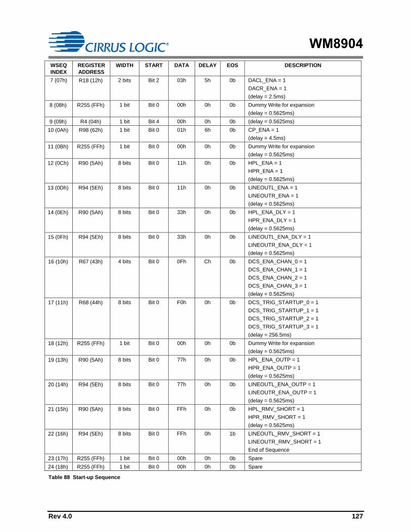
WM8904
Rev 4.0 127
WSEQ
INDEX
REGISTER
ADDRESS
WIDTH START DATA DELAY EOS DESCRIPTION
7 (07h) R18 (12h) 2 bits Bit 2 03h 5h 0b DACL_ENA = 1
DACR_ENA = 1
(delay = 2.5ms)
8 (08h) R255 (FFh) 1 bit Bit 0 00h 0h 0b Dummy Write for expansion
(delay = 0.5625ms)
9 (09h) R4 (04h) 1 bit Bit 4 00h 0h 0b (delay = 0.5625ms)
10 (0Ah) R98 (62h) 1 bit Bit 0 01h 6h 0b CP_ENA = 1
(delay = 4.5ms)
11 (0Bh) R255 (FFh) 1 bit Bit 0 00h 0h 0b Dummy Write for expansion
(delay = 0.5625ms)
12 (0Ch) R90 (5Ah) 8 bits Bit 0 11h 0h 0b HPL_ENA = 1
HPR_ENA = 1
(delay = 0.5625ms)
13 (0Dh) R94 (5Eh) 8 bits Bit 0 11h 0h 0b LINEOUTL_ENA = 1
LINEOUTR_ENA = 1
(delay = 0.5625ms)
14 (0Eh) R90 (5Ah) 8 bits Bit 0 33h 0h 0b HPL_ENA_DLY = 1
HPR_ENA_DLY = 1
(delay = 0.5625ms)
15 (0Fh) R94 (5Eh) 8 bits Bit 0 33h 0h 0b LINEOUTL_ENA_DLY = 1
LINEOUTR_ENA_DLY = 1
(delay = 0.5625ms)
16 (10h) R67 (43h) 4 bits Bit 0 0Fh Ch 0b DCS_ENA_CHAN_0 = 1
DCS_ENA_CHAN_1 = 1
DCS_ENA_CHAN_2 = 1
DCS_ENA_CHAN_3 = 1
(delay = 0.5625ms)
17 (11h) R68 (44h) 8 bits Bit 0 F0h 0h 0b DCS_TRIG_STARTUP_0 = 1
DCS_TRIG_STARTUP_1 = 1
DCS_TRIG_STARTUP_2 = 1
DCS_TRIG_STARTUP_3 = 1
(delay = 256.5ms)
18 (12h) R255 (FFh) 1 bit Bit 0 00h 0h 0b Dummy Write for expansion
(delay = 0.5625ms)
19 (13h) R90 (5Ah) 8 bits Bit 0 77h 0h 0b HPL_ENA_OUTP = 1
HPR_ENA_OUTP = 1
(delay = 0.5625ms)
20 (14h) R94 (5Eh) 8 bits Bit 0 77h 0h 0b LINEOUTL_ENA_OUTP = 1
LINEOUTR_ENA_OUTP = 1
(delay = 0.5625ms)
21 (15h) R90 (5Ah) 8 bits Bit 0 FFh 0h 0b HPL_RMV_SHORT = 1
HPR_RMV_SHORT = 1
(delay = 0.5625ms)
22 (16h) R94 (5Eh) 8 bits Bit 0 FFh 0h 1b LINEOUTL_RMV_SHORT = 1
LINEOUTR_RMV_SHORT = 1
End of Sequence
23 (17h) R255 (FFh) 1 bit Bit 0 00h 0h 0b Spare
24 (18h) R255 (FFh) 1 bit Bit 0 00h 0h 0b Spare
Table 88 Start-up Sequence

WM8904
128 Rev 4.0
SHUTDOWN SEQUENCE
The Shutdown sequence is initiated by writing 0119h to Register R111 (6Fh). This single operation
starts the Control Write Sequencer at Index Address 25 (19h) and executes the sequence defined in
Table 89.
For typical clocking configurations with MCLK=12.288MHz, this sequence takes approximately 350ms.
WSEQ
INDEX
REGISTER
ADDRESS
WIDTH START DATA DELAY EOS DESCRIPTION
25 (19h) R94 (5Eh) 8 bits Bit 0 77h 0h 0b LINEOUTL_RMV_SHORT = 0
LINEOUTR_RMV_SHORT = 0
(delay = 0.5625ms)
26 (1Ah) R90 (5Ah) 8 bits Bit 0 77h 0h 0b HPL_RMV_SHORT = 0
HPR_RMV_SHORT = 0
(delay = 0.5625ms)
27 (1Bh) R90 (5Ah) 8 bits Bit 0 00h 0h 0b HPL_ENA_OUTP = 0
HPL_ENA_DLY = 0
HPL_ENA = 0
HPR_ENA_OUTP = 0
HPR_ENA_DLY = 0
HPR_ENA = 0
(delay = 0.5625ms)
28 (1Ch) R94 (5Eh) 8 bits Bit 0 00h 0h 0b LINEOUTL_ENA_OUTP = 0
LINEOUTL_ENA_DLY = 0
LINEOUTL_ENA = 0
LINEOUTR_ENA_OUTP = 0
LINEOUTR_ENA_DLY = 0
LINEOUTR_ENA = 0
(delay = 0.5625ms)
29 (1Dh) R67 (43h) 4 bits Bit 0 00h 0h 0b DCS_ENA_CHAN_0 = 0
DCS_ENA_CHAN_1 = 0
DCS_ENA_CHAN_2 = 0
DCS_ENA_CHAN_3 = 0
(delay = 0.5625ms)
30 (1Eh) R98 (62h) 1 bit Bit 0 00h 0h 0b CP_ENA = 0
(delay = 0.5625ms)
31 (1Fh) R18 (12h) 2 bits Bit 2 00h 0h 0b DACL_ENA = 0
DACR_ENA = 0
(delay = 0.5625ms)
32 (20h) R22 (16h) 1 bit Bit 1 00h 0h 0b CLK_DSP_ENA = 0
(delay = 0.5625ms)
33 (21h) R14 (0Eh) 2 bits Bit 0 00h 0h 0b HPL_PGA_ENA = 0
HPR_PGA_ENA = 0
(delay = 0.5625ms)
34 (22h) R15 (0Fh) 2 bits Bit 0 00h 0h 0b LINEOUTL_PGA_ENA = 0
LINEOUTR_PGA_ENA = 0
(delay = 0.5625ms)
35 (23h) R4 (04h) 1 bit Bit 0 00h 0h 0b BIAS_ENA = 0
(delay = 0.5625ms)
36 (24h) R5 (05h) 1 bit Bit 0 00h Ch 0b VMID_ENA = 0
(delay = 256.5ms)
37 (25h) R5 (05h) 1 bit Bit 0 00h 9h 0b VMID_ENA = 0
(delay = 32.5ms)
38 (26h) R5 (05h) 8 bits Bit 0 00h 0h 0b VMID_BUF_ENA = 0
VMID_RES[1:0] = 00
VMID_ENA = 0

WM8904
Rev 4.0 129
WSEQ
INDEX
REGISTER
ADDRESS
WIDTH START DATA DELAY EOS DESCRIPTION
(delay = 0.5625ms)
39 (27h) R4 (04h) 2 bits Bit 0 00h 0h 1b BIAS_ENA = 0
End of Sequence
Table 89 Shutdown Sequence
POWER-ON RESET
The WM8904 includes an internal Power-On-Reset (POR) circuit, which is used to reset the digital
logic into a default state after power up. The POR circuit is powered from AVDD and monitors
DCVDD. The internal POR¯¯¯ signal is asserted low when AVDD or DCVDD are below minimum
thresholds.
The specific behaviour of the circuit will vary, depending on the relative timing of the supply voltages.
Typical scenarios are illustrated in Figure 69 and Figure 70.
DCVDD
Vpord_on
0V
AVDD
0V
Vpora
Vpora_off
LO
HI
Internal POR
Device readyPOR active POR active
POR undefined
Figure 69 Power On Reset timing - AVDD enabled first

WM8904
130 Rev 4.0
DCVDD
0V
AVDD
0V
Vpora
Vpord_off
LO
HI
Internal POR
Device ready
Vpora_on
POR active POR active
POR undefined
Figure 70 Power On Reset timing - DCVDD enabled first
The POR¯¯¯ signal is undefined until AVDD has exceeded the minimum threshold, Vpora Once this
threshold has been exceeded, POR¯¯¯ is asserted low and the chip is held in reset. In this condition, all
writes to the control interface are ignored. Once AVDD and DCVDD have reached their respective
power on thresholds, POR¯¯¯ is released high, all registers are in their default state, and writes to the
control interface may take place.
Note that a minimum power-on reset period, TPOR, applies even if AVDD and DCVDD have zero rise
time. (This specification is guaranteed by design rather than test.)
On power down, POR¯¯¯ is asserted low when any of AVDD or DCVDD falls below their respective
power-down thresholds.
Typical Power-On Reset parameters for the WM8904 are defined in Table 90.
SYMBOL DESCRIPTION TYP UNIT
Vpora AVDD threshold below which POR is undefined 0.25 V
Vpora_on Power-On threshold (AVDD) 1.15 V
Vpora_off Power-Off threshold (AVDD) 1.12 V
Vpord_on Power-On threshold (DCVDD) 0.57 V
Vpord_off Power-Off threshold (DCVDD) 0.55 V
TPOR Minimum Power-On Reset period 9.5 s
Table 90 Typical Power-On Reset parameters
Notes:
1. If AVDD and DCVDD suffer a brown-out (i.e. drop below the minimum recommended operating
level but do not go below Vpora_off or Vpord_off) then the chip does not reset and resumes normal
operation when the voltage is back to the recommended level again.
2. The chip enters reset at power down when AVDD or DCVDD falls below Vpora_off or Vpord_off. This
may be important if the supply is turned on and off frequently by a power management system.
3. The minimum Tpor period is maintained even if DCVDD and AVDD have zero rise time. This
specification is guaranteed by design rather than test.

WM8904
Rev 4.0 131
QUICK START-UP AND SHUTDOWN
The WM8904 has the capability to perform a quick start-up and shutdown with a minimum number of
register operations. This is achieved using the Control Write Sequencer, which is configured with
default start-up settings that set up the device for DAC playback via Headphone and Line output.
Assuming a 12.288MHz external clock, the start-up sequence configures the device for 48kHz
playback mode.
The default start-up sequence requires three register write operations. The default shutdown
sequence requires just a single register write. The minimum procedure for executing the quick start-up
and shutdown sequences is described below. See “Control Write Sequencer” for more details.
After the default start-up sequence has been performed, the DC offset correction values will be held in
memory, provided that power is maintained and a software reset is not performed. Fast start-up using
the stored values of DC offset correction is also possible, as described below.
QUICK START-UP (DEFAULT SEQUENCE)
An external clock must be applied to MCLK. Assuming 12.288MHz input clock, the start-up sequence
will take approximately 300ms to complete.
The following register operations will initiate the quick start-up sequence.
REGISTER
ADDRESS
VALUE DESCRIPTION
R108 (6Ch)
Write Sequencer 0
0100h WSEQ_ENA = 1
WSEQ_WRITE_INDEX = 00h
This enables the Write Sequencer
R111 (6Fh)
Write Sequencer 3
0100h WSEQ_ABORT = 0
WSEQ_START = 1
WSEQ_START_INDEX = 00h
This starts the Write Sequencer at Index address 0 (00h)
R33 (21h)
DAC Digital 1
0000h DAC_MONO = 0
DAC_SB_FILT = 0
DAC_MUTERATE = 0
DAC_UNMUTE_RAMP = 0
DAC_OSR128 = 0
DAC_MUTE = 0
DEEMPH = 00
This un-mutes the DACs
Table 91 Quick Start-up Control
The WSEQ_BUSY bit (in Register R112, see Table 85) will be set to 1 while the sequence runs. When
this bit returns to 0, the device has been set up and is ready for DAC playback operation.

WM8904
132 Rev 4.0
FAST START-UP FROM STANDBY
The default start-up sequence runs the DC Servo to remove DC offsets from the outputs. The offset
for this path selection is then stored in memory. Provided that power is maintained to the chip, and a
software reset is not performed, then the DC offset correction will be held in memory on the WM8904.
This allows the DC Servo calibrations to be omitted from the start-up sequence if the offset correction
has already been performed. By omitting this part of the start-up sequence, a fast start-up time of less
than 50ms can be achieved.
The register write sequence described in Table 92 replaces the default DC Servo operation with
dummy operations, allowing a fast start-up to be achieved, assuming the device is initially in a standby
condition with DC offset correction previously performed.
Note that, if power is removed from the WM8904 or if a software reset is performed, then the default
sequence will be restored, and the DC offset correction will be necessary on the output paths once
more.
REGISTER
ADDRESS VALUE DESCRIPTION
R108 (6Ch)
Write Sequencer 0
0111h WSEQ_ENA = 1
WSEQ_WRITE_INDEX = 11h
This enables the Write Sequencer and selects WSEQ
Index 17 (11h) for modification
R109 (6Dh)
Write Sequencer 1
00FFh WSEQ_DATA_WIDTH = 000
WSEQ_DATA_START = 0000
WSEQ_ADDR = FFh
This modifies WSEQ Index 17 (11h) with Dummy step
R110 (6Eh)
Write Sequencer 2
0000h WSEQ_EOS = 0
WSEQ_DELAY = 0000
WSEQ_DATA = 00h
This modifies WSEQ Index 17 (11h) with Dummy step
R111 (6Fh)
Write Sequencer 3
0100h WSEQ_ABORT = 0
WSEQ_START = 1
WSEQ_START_INDEX = 00h
This starts the Write Sequencer at Index address 0 (00h)
R33 (21h)
DAC Digital 1
0000h DAC_MONO = 0
DAC_SB_FILT = 0
DAC_MUTERATE = 0
DAC_UNMUTE_RAMP = 0
DAC_OSR128 = 0
DAC_MUTE = 0
DEEMPH = 00
This un-mutes the DACs
Table 92 Fast Start-up from Standby Control
The WSEQ_BUSY bit (in Register R112, see Table 85) will be set to 1 while the sequence runs. When
this bit returns to 0, the device has been set up and is ready for DAC playback operation.

WM8904
Rev 4.0 133
QUICK SHUTDOWN (DEFAULT SEQUENCE)
The default shutdown sequence assumes the initial device conditions are as configured by the default
start-up sequence. Assuming 12.288MHz input clock, the shutdown sequence will take approximately
350ms to complete.
The following register operation will initiate the default shutdown sequence.
REGISTER
ADDRESS VALUE DESCRIPTION
R111 (6Fh)
Write Sequencer 3
0119h WSEQ_ABORT = 0
WSEQ_START = 1
WSEQ_START_INDEX = 19h
This starts the Write Sequencer at Index address 25 (19h)
Table 93 Quick Shutdown Control
The WSEQ_BUSY bit (in Register R112, see Table 85) will be set to 1 while the sequence runs. When
this bit returns to 0, the system clock can be disabled (CLK_SYS_ENA=0) and MCLK can be stopped.
SOFTWARE RESET AND CHIP ID
A Software Reset can be commanded by writing to Register R0. This is a read-only register field and
the contents will not be affected by writing to this Register.
The Chip ID can be read back from Register R0.
REGISTER
ADDRESS
BIT LABEL DEFAULT DESCRIPTION
R0 (00h)
SW Reset
and ID
15:0 SW_RST_DE
V_ID1 [15:0]
8904h Writing to this register resets all
registers to their default state.
Reading from this register will indicate
Device ID 8904h.
Table 94 Software Reset and Chip ID

WM8904
134 Rev 4.0
REGISTER MAP
De
c A
dd
rH
ex
Ad
dr
Na
me
15
14
13
12
11
10
98
76
54
32
10
Bin
De
fa
ult
00
0S
W R
eset
and
ID
100
0_
100
1_0
00
0_
010
0
40
4B
ias C
ontr
ol 0
00
00
00
00
00
01
0B
IAS
_E
NA
00
00
_0
00
0_
00
01_
100
0
50
5V
MID
Co
ntr
ol 0
00
00
00
00
0V
MID
_B
UF
_E
NA
00
0V
MID
_E
NA
00
00
_0
00
0_
00
00
_0
00
0
60
6M
ic B
ias C
ontr
ol 0
00
00
00
00
0M
ICD
ET
_E
NA
MIC
BIA
S_
EN
A0
00
0_
00
00
_0
00
0_
00
00
70
7M
ic B
ias C
ontr
ol 1
00
00
00
00
00
00
00
00
0_
00
00
_0
00
0_
00
00
100
AA
nalo
gue A
DC
00
00
00
00
00
00
00
00
AD
C_
OS
R12
80
00
0_
00
00
_0
00
0_
00
01
120
CP
ow
er
Manag
em
ent
00
00
00
00
00
00
00
0IN
L_
EN
AIN
R_
EN
A0
00
0_
00
00
_0
00
0_
00
00
140
EP
ow
er
Manag
em
ent
20
00
00
00
00
00
00
0H
PL_
PG
A_
EN
AH
PR
_P
GA
_E
NA
00
00
_0
00
0_
00
00
_0
00
0
150
FP
ow
er
Manag
em
ent
30
00
00
00
00
00
00
0LIN
EO
UT
L_
PG
A_
EN
A
LIN
EO
UT
R_
PG
A_
E
NA
00
00
_0
00
0_
00
00
_0
00
0
1812
Po
wer
Manag
em
ent
60
00
00
00
00
00
0D
AC
L_
EN
AD
AC
R_
EN
AA
DC
L_
EN
AA
DC
R_
EN
A0
00
0_
00
00
_0
00
0_
00
00
20
14C
lock R
ate
s 0
1T
OC
LK
_R
AT
E_
DIV
1
6T
OC
LK
_R
AT
E_
X4
01
10
00
10
11
11
MC
LK
_D
IV10
00
_11
00
_0
101_
1110
21
15C
lock R
ate
s 1
00
00
00
00
00
00
0_
110
0_
00
00
_0
101
22
16C
lock R
ate
s 2
MC
LK
_IN
VS
YS
CLK
_S
RC
0T
OC
LK
_R
AT
E0
00
00
00
0O
PC
LK
_E
NA
CLK
_S
YS
_E
NA
CLK
_D
SP
_E
NA
TO
CLK
_E
NA
00
00
_0
00
0_
00
00
_0
00
0
24
18A
ud
io Inte
rface 0
00
0D
AC
L_
DA
TIN
VD
AC
R_
DA
TIN
VLO
OP
BA
CK
AIF
AD
CL_
SR
CA
IFA
DC
R_
SR
CA
IFD
AC
L_
SR
CA
IFD
AC
R_
SR
CA
DC
_C
OM
PA
DC
_C
OM
PM
OD
ED
AC
_C
OM
PD
AC
_C
OM
PM
OD
E0
00
0_
00
00
_0
101_
00
00
25
19A
ud
io Inte
rface 1
00
AIF
DA
C_
TD
MA
IFD
AC
_T
DM
_C
H
AN
AIF
AD
C_
TD
MA
IFA
DC
_T
DM
_C
H
AN
0A
IF_
TR
ISA
IF_
BC
LK
_IN
VB
CLK
_D
IR0
AIF
_LR
CLK
_IN
V0
00
0_
00
00
_0
00
0_
1010
26
1AA
ud
io Inte
rface 2
00
00
11
10
00
0_
00
00
_11
10_
010
0
27
1BA
ud
io Inte
rface 3
00
00
LR
CLK
_D
IR0
00
0_
00
00
_0
100
_0
00
0
30
1ED
AC
Dig
ital V
olu
me L
eft
00
00
00
0D
AC
_V
U0
00
0_
00
0P
_11
00
_0
00
0
31
1FD
AC
Dig
ital V
olu
me R
ight
00
00
00
0D
AC
_V
U0
00
0_
00
0P
_11
00
_0
00
0
32
20
DA
C D
igit
al 0
00
00
00
00
_0
00
0_
00
00
_0
00
0
33
21
DA
C D
igit
al 1
00
0D
AC
_M
ON
OD
AC
_S
B_
FIL
TD
AC
_M
UT
ER
AT
ED
AC
_U
NM
UT
E_
RA
MP
00
DA
C_
OS
R12
80
0D
AC
_M
UT
E0
00
00
_0
00
0_
00
00
_10
00
36
24
AD
C D
igit
al V
olu
me L
eft
00
00
00
0A
DC
_V
U0
00
0_
00
0P
_11
00
_0
00
0
37
25
AD
C D
igit
al V
olu
me R
ight
00
00
00
0A
DC
_V
U0
00
0_
00
0P
_11
00
_0
00
0
38
26
AD
C D
igit
al 0
00
00
00
00
0A
DC
_H
PF
00
AD
CL_
DA
TIN
VA
DC
R_
DA
TIN
V0
00
0_
00
00
_0
00
1_0
00
0
39
27
Dig
ital M
icro
pho
ne 0
00
0D
MIC
_E
NA
DM
IC_
SR
C0
00
00
00
00
00
00
00
_0
00
0_
00
00
_0
00
0
40
28
DR
C 0
DR
C_
EN
AD
RC
_D
AC
_P
AT
H0
DR
C_
FF
_D
ELA
Y0
DR
C_
GS
_E
NA
DR
C_
QR
DR
C_
AN
TIC
LIP
DR
C_
GS
_H
YS
T0
00
0_
00
01_
1010
_11
11
41
29
DR
C 1
00
11_
00
10_
010
0_
100
0
42
2A
DR
C 2
00
00
00
00
00
00
00
_0
00
0_
00
00
_0
00
0
43
2B
DR
C 3
00
00
00
00
0_
00
00
_0
00
0_
00
00
ISE
L [
1:0
]
LR
CLK
_R
AT
E[1
0:0
]
DR
C_
KN
EE
_O
P[4
:0]
DR
C_
HI_
CO
MP
[2:0
]
DR
C_
AT
K[3
:0]
DR
C_
DC
Y[3
:0]
DR
C_
MA
XG
AIN
[1:0
]
DR
C_
KN
EE
_IP
[5:0
]
DR
C_
MIN
GA
IN[1
:0]
DR
C_
QR
_T
HR
[1:0
]
DR
C_
LO
_C
OM
P[2
:0]
DE
EM
PH
[1:0
]
AIF
_W
L[1
:0]
DA
CR
_V
OL[7
:0]
DA
CL_
VO
L[7
:0]
AIF
_F
MT
[1:0
]
AD
CR
_V
OL[7
:0]
DR
C_
QR
_D
CY
[1:0
]
AD
CL_
VO
L[7
:0]
OP
CLK
_D
IV[3
:0]
BC
LK
_D
IV[4
:0]
SW
_R
ST
_D
EV
_ID
1[15
:0]
VM
ID_
RE
S[1
:0]
MIC
SH
OR
T_
TH
R[1
:0]
MIC
DE
T_
TH
R[2
:0]
MIC
BIA
S_
SE
L[2
:0]
CLK
_S
YS
_R
AT
E[3
:0]
DA
C_
BO
OS
T[1
:0]
SA
MP
LE
_R
AT
E[2
:0]
AD
CL_
DA
C_
SV
OL[3
:0]
DR
C_
ST
AR
TU
P_
GA
IN[4
:0]
AD
CR
_D
AC
_S
VO
L[3
:0]
DR
C_
GS
_H
YS
T_
LV
L[1
:0]
AD
C_
TO
_D
AC
R[1
:0]
AD
C_
TO
_D
AC
L[1
:0]
AD
C_
HP
F_
CU
T[1
:0]

WM8904
Rev 4.0 135
Dec
Ad
dr
Hex
Ad
dr
Nam
e1
51
41
31
21
11
09
87
65
43
21
0B
in D
efa
ult
44
2C
An
alo
gu
e L
eft
In
pu
t 0
00
00
00
00
LIN
MU
TE
00
00
00
_0
00
0_
10
00
_0
10
1
45
2D
An
alo
gu
e R
igh
t In
pu
t 0
00
00
00
00
RIN
MU
TE
00
00
00
_0
00
0_
10
00
_0
10
1
46
2E
An
alo
gu
e L
eft
In
pu
t 1
00
00
00
00
0IN
L_
CM
_E
NA
00
00
_0
00
0_
01
00
_0
10
0
47
2F
An
alo
gu
e R
igh
t In
pu
t 1
00
00
00
00
0IN
R_C
M_
EN
A0
00
0_
00
00
_0
10
0_
01
00
57
39
An
alo
gu
e O
UT
1 L
eft
00
00
00
0H
PO
UT
L_M
UT
EH
PO
UT
_V
UH
PO
UT
LZ
C0
00
0_
00
00
_P
01
0_
11
01
58
3A
An
alo
gu
e O
UT
1 R
igh
t0
00
00
00
HP
OU
TR
_MU
TE
HP
OU
T_
VU
HP
OU
TR
ZC
00
00
_0
00
0_
P0
10
_1
10
1
59
3B
An
alo
gu
e O
UT
2 L
eft
00
00
00
0LI
NE
OU
TL_
MU
TE
LIN
EO
UT
_V
UL
INE
OU
TL
ZC
00
00
_0
00
0_
P0
11
_1
00
1
60
3C
An
alo
gu
e O
UT
2 R
igh
t0
00
00
00
LIN
EO
UT
R_M
UT
EL
INE
OU
T_
VU
LIN
EO
UT
RZ
C0
00
0_
00
00
_P
01
1_
10
01
61
3D
An
alo
gu
e O
UT
12
ZC
00
00
00
00
00
00
HP
L_
BY
P_
EN
AH
PR
_B
YP
_E
NA
LIN
EO
UT
L_
BY
P_
EN
A
LIN
EO
UT
R_B
YP
_E
NA
00
00
_0
00
0_
00
00
_0
00
0
67
43
DC
Se
rvo
00
00
00
00
00
00
0D
CS
_E
NA
_C
HA
N
_3
DC
S_
EN
A_
CH
AN
_2
DC
S_
EN
A_
CH
AN
_1
DC
S_
EN
A_
CH
AN
_0
00
00
_0
00
0_
00
00
_0
00
0
68
44
DC
Se
rvo
1D
CS
_T
RIG
_S
ING
LE
_3
DC
S_
TR
IG_
SIN
G
LE
_2
DC
S_
TR
IG_
SIN
G
LE
_1
DC
S_
TR
IG_
SIN
G
LE
_0
DC
S_
TR
IG_
SE
RI
ES
_3
DC
S_
TR
IG_
SE
RI
ES
_2
DC
S_
TR
IG_
SE
RI
ES
_1
DC
S_
TR
IG_
SE
RI
ES
_0
DC
S_
TR
IG_
ST
A
RT
UP
_3
DC
S_
TR
IG_
ST
A
RT
UP
_2
DC
S_
TR
IG_
ST
A
RT
UP
_1
DC
S_
TR
IG_
ST
A
RT
UP
_0
DC
S_
TR
IG_
DA
C
_W
R_3
DC
S_
TR
IG_
DA
C
_W
R_2
DC
S_
TR
IG_
DA
C
_W
R_1
DC
S_
TR
IG_
DA
C
_W
R_0
PP
PP
_P
PP
P_
PP
PP
_P
PP
P
69
45
DC
Se
rvo
20
00
00
00
01
01
0_
10
10
_1
01
0_
10
10
71
47
DC
Se
rvo
40
00
00
00
00
10
10
_1
01
0_
10
10
_1
01
0
72
48
DC
Se
rvo
50
00
00
00
00
10
10
_1
01
0_
10
10
_1
01
0
73
49
DC
Se
rvo
60
00
00
00
00
00
0_
00
00
_0
00
0_
00
00
74
4A
DC
Se
rvo
70
00
00
00
00
00
0_
00
00
_0
00
0_
00
00
75
4B
DC
Se
rvo
80
00
00
00
00
00
0_
00
00
_0
00
0_
00
00
76
4C
DC
Se
rvo
90
00
00
00
00
00
0_
00
00
_0
00
0_
00
00
77
4D
DC
Se
rvo
Re
ad
ba
ck 0
00
00
00
00
_0
00
0_
00
00
_0
00
0
90
5A
An
alo
gu
e H
P 0
00
00
00
00
HP
L_
RM
V_
SH
O
RT
HP
L_
EN
A_
OU
TP
HP
L_
EN
A_
DLY
HP
L_
EN
AH
PR
_R
MV
_S
HO
RT
HP
R_E
NA
_O
UT
PH
PR
_E
NA
_D
LY
HP
R_E
NA
00
00
_0
00
0_
00
00
_0
00
0
94
5E
An
alo
gu
e L
ine
ou
t 0
00
00
00
00
LIN
EO
UT
L_
RM
V
_S
HO
RT
LIN
EO
UT
L_
EN
A_
OU
TP
LIN
EO
UT
L_
EN
A_
DLY
LIN
EO
UT
L_
EN
AL
INE
OU
TR
_R
MV
_S
HO
RT
LIN
EO
UT
R_E
NA
_O
UT
P
LIN
EO
UT
R_E
NA
_D
LY
LIN
EO
UT
R_E
NA
00
00
_0
00
0_
00
00
_0
00
0
98
62
Cha
rge
Pu
mp
00
00
00
00
00
00
00
00
CP
_E
NA
00
00
_0
00
0_
00
00
_0
00
0
10
46
8C
lass
W 0
00
00
00
00
00
00
00
0C
P_D
YN
_PW
R00
00_0
000_
0000
_010
0
10
86
CW
rite
Se
qu
en
ce
r 0
00
00
00
0W
SE
Q_
EN
A0
00
00
00
_0
00
0_
00
00
_0
00
0
10
96
DW
rite
Se
qu
en
ce
r 1
00
00
0_
00
00
_0
00
0_
00
00
11
06
EW
rite
Se
qu
en
ce
r 2
0W
SE
Q_
EO
S0
00
00
0_
00
00
_0
00
0_
00
00
11
16
FW
rite
Se
qu
en
ce
r 3
00
00
00
WS
EQ
_A
BO
RT
WS
EQ
_S
TA
RT
00
00
00
_0
00
0_
00
00
_0
00
0
11
27
0W
rite
Se
qu
en
ce
r 4
00
00
00
00
0W
SE
Q_
BU
SY
00
00
_0
00
0_
00
00
_0
00
0
DC
S_
DA
C_W
R_V
AL
_2
[7:0
]
WS
EQ
_D
AT
A_
WID
TH
[2:0
]
WS
EQ
_D
AT
A[7
:0]
WS
EQ
_D
AT
A_
ST
AR
T[3
:0]
WS
EQ
_S
TA
RT
_IN
DE
X[5
:0]
DC
S_
SE
RIE
S_
NO
_2
3[6
:0]
L_
MO
DE
[1:0
]
LIN
_V
OL
[4:0
]
RIN
_V
OL
[4:0
]
DC
S_
TIM
ER
_P
ER
IOD
_0
1[3
:0]
HP
OU
TL
_V
OL
[5:0
]
HP
OU
TR
_V
OL
[5:0
]
DC
S_
TIM
ER
_P
ER
IOD
_2
3[3
:0]
R_IP
_S
EL
_P
[1:0
]R
_IP
_S
EL
_N
[1:0
]
LIN
EO
UT
L_
VO
L[5
:0]
DC
S_
SE
RIE
S_
NO
_0
1[6
:0]
DC
S_
DA
C_W
R_V
AL
_3
[7:0
]
DC
S_
DA
C_W
R_V
AL
_1
[7:0
]
R_M
OD
E[1
:0]
L_
IP_
SE
L_
P[1
:0]
L_
IP_
SE
L_
N[1
:0]
LIN
EO
UT
R_V
OL
[5:0
]
WS
EQ
_D
EL
AY
[3:0
]
WS
EQ
_C
UR
RE
NT
_IN
DE
X[5
:0]
WS
EQ
_W
RIT
E_
IND
EX
[4:0
]
WS
EQ
_A
DD
R[7
:0]
DC
S_
DA
C_W
R_V
AL
_0
[7:0
]
DC
S_
DA
C_W
R_C
OM
PL
ET
E[3
:0]
DC
S_
CA
L_
CO
MP
LE
TE
[3:0
]D
CS
_S
TA
RT
UP
_C
OM
PL
ET
E[3
:0]

WM8904
136 Rev 4.0
Dec
Ad
dr
Hex
Ad
dr
Nam
e1
51
41
31
21
11
09
87
65
43
21
0B
in D
efa
ult
11
67
4F
LL
Co
ntr
ol 1
00
00
00
00
00
00
0F
LL_F
RA
CN
_EN
AF
LL_O
SC
_EN
AF
LL_E
NA
00
00
_0
00
0_
00
00
_0
00
0
11
77
5F
LL
Co
ntr
ol 2
00
00
00
00
_0
00
0_
00
00
_0
11
1
11
87
6F
LL
Co
ntr
ol 3
00
00
_0
00
0_
00
00
_0
00
0
11
97
7F
LL
Co
ntr
ol 4
00
00
10
_1
11
0_
11
10
_0
00
0
12
07
8F
LL
Co
ntr
ol 5
00
00
00
00
00
01
00
00
_0
00
0_
00
00
_0
10
0
12
17
9G
PIO
Co
ntr
ol 1
00
00
00
00
00
GP
IO1_
PU
GP
IO1_
PD
00
00
_0
00
0_
00
01
_0
10
0
12
27
AG
PIO
Co
ntr
ol 2
00
00
00
00
00
GP
IO2_
PU
GP
IO2_
PD
00
00
_0
00
0_
00
01
_0
00
0
12
37
BG
PIO
Co
ntr
ol 3
00
00
00
00
00
GP
IO3_
PU
GP
IO3_
PD
00
00
_0
00
0_
00
01
_0
00
0
12
47
CG
PIO
Co
ntr
ol 4
00
00
00
GP
I7_
EN
AG
PI8
_E
NA
GP
IO_
BC
LK
_M
O
DE
_E
NA
00
00
00
0_
00
00
_0
00
0_
00
00
12
67
ED
igita
l P
ulls
00
00
00
00
MC
LK
_P
UM
CLK
_P
DD
AC
DA
T_
PU
DA
CD
AT
_P
DL
RC
LK
_P
UL
RC
LK
_P
DB
CLK
_P
UB
CLK
_P
D0
00
0_
00
00
_0
00
0_
00
00
12
77
FIn
terr
up
t S
tatu
s0
00
00
IRQ
GP
IO_
BC
LK
_E
IN
TW
SE
Q_
EIN
TG
PIO
3_
EIN
TG
PIO
2_
EIN
TG
PIO
1_
EIN
TG
PI8
_E
INT
GP
I7_
EIN
TF
LL
_L
OC
K_
EIN
TM
IC_
SH
RT
_E
INT
MIC
_D
ET
_E
INT
XX
XX
_X
PP
P_
PP
PP
_P
PP
P
12
88
0In
terr
up
t S
tatu
s M
ask
00
00
00
IM_
GP
IO_
BC
LK
_
EIN
TIM
_W
SE
Q_
EIN
TIM
_G
PIO
3_
EIN
TIM
_G
PIO
2_
EIN
TIM
_G
PIO
1_
EIN
TIM
_G
PI8
_E
INT
IM_
GP
I7_
EIN
TIM
_F
LL
_L
OC
K_
E
INT
IM_
MIC
_S
HR
T_
E
INT
IM_
MIC
_D
ET
_E
I
NT
11
11
_1
11
1_
11
11
_1
11
1
12
98
1In
terr
up
t P
ola
rity
00
00
00
GP
IO_
BC
LK
_E
IN
T_
PO
L
WS
EQ
_E
INT
_P
O
L
GP
IO3
_E
INT
_P
O
L
GP
IO2
_E
INT
_P
O
L
GP
IO1
_E
INT
_P
O
LG
PI8
_E
INT
_P
OL
GP
I7_
EIN
T_
PO
LF
LL
_L
OC
K_
EIN
T
_P
OL
MIC
_S
HR
T_
EIN
T
_P
OL
MIC
_D
ET
_E
INT
_
PO
L0
00
0_
00
00
_0
00
0_
00
00
13
08
2In
terr
up
t D
eb
ou
nce
00
00
00
GP
IO_
BC
LK
_E
IN
T_
DB
WS
EQ
_E
INT
_D
BG
PIO
3_
EIN
T_
DB
GP
IO2
_E
INT
_D
BG
PIO
1_
EIN
T_
DB
GP
I8_
EIN
T_
DB
GP
I7_
EIN
T_
DB
FL
L_
LO
CK
_E
INT
_D
B
MIC
_S
HR
T_
EIN
T
_D
B
MIC
_D
ET
_E
INT
_
DB
00
00
_0
00
0_
00
00
_0
00
0
13
48
6E
Q1
00
00
00
00
00
00
00
0E
Q_
EN
A0
00
0_
00
00
_0
00
0_
00
00
13
58
7E
Q2
00
00
00
00
00
00
00
0_
00
00
_0
00
0_
11
00
13
68
8E
Q3
00
00
00
00
00
00
00
0_
00
00
_0
00
0_
11
00
13
78
9E
Q4
00
00
00
00
00
00
00
0_
00
00
_0
00
0_
11
00
13
88
AE
Q5
00
00
00
00
00
00
00
0_
00
00
_0
00
0_
11
00
13
98
BE
Q6
00
00
00
00
00
00
00
0_
00
00
_0
00
0_
11
00
14
08
CE
Q7
00
00
_1
11
1_
11
00
_1
01
0
14
18
DE
Q8
00
00
_0
10
0_
00
00
_0
00
0
14
28
EE
Q9
00
00
_0
00
0_
11
01
_1
00
0
14
38
FE
Q1
00
00
1_
11
10
_1
01
1_
01
01
14
49
0E
Q1
11
11
1_
00
01
_0
10
0_
01
01
14
59
1E
Q1
20
00
0_
10
11
_0
11
1_
01
01
14
69
2E
Q1
30
00
0_
00
01
_1
10
0_
01
01
14
79
3E
Q1
40
00
1_
11
00
_0
10
1_
10
00
14
89
4E
Q1
51
11
1_
00
11
_0
11
1_
00
11
14
99
5E
Q1
60
00
0_
10
10
_0
10
1_
01
00
15
09
6E
Q1
70
00
0_
01
01
_0
10
1_
10
00
15
19
7E
Q1
80
00
1_
01
10
_1
00
0_
11
10
FLL
_CLK
_RE
F_D
IV[1
:0]
FLL
_CLK
_RE
F_S
RC
[1:0
]
EQ
_B
5_
GA
IN[4
:0]
EQ
_B
1_
A[1
5:0
]
GP
IO_
BC
LK
_S
EL
[3:0
]
FLL
_CT
RL_
RA
TE
[2:0
]F
LL_F
RA
TIO
[2:0
]
FLL
_K[1
5:0]
FL
L_
OU
TD
IV[5
:0]
EQ
_B
3_
A[1
5:0
]
EQ
_B
2_
B[1
5:0
]
EQ
_B
2_
C[1
5:0
]
EQ
_B
3_
GA
IN[4
:0]
EQ
_B
4_
GA
IN[4
:0]
FLL
_GA
IN[3
:0]
GP
IO2
_S
EL
[3:0
]
EQ
_B
1_
PG
[15
:0]
EQ
_B
2_
PG
[15
:0]
EQ
_B
1_
GA
IN[4
:0]
EQ
_B
2_
GA
IN[4
:0]
EQ
_B
1_
B[1
5:0
]
EQ
_B
3_
C[1
5:0
]
EQ
_B
3_
B[1
5:0
]
FLL
_N[9
:0]
EQ
_B
2_
A[1
5:0
]
GP
IO1
_S
EL
[3:0
]
GP
IO3
_S
EL
[3:0
]
EQ
_B
4_
A[1
5:0
]
EQ
_B
3_
PG
[15
:0]

WM8904
Rev 4.0 137
Dec
Ad
dr
Hex
Ad
dr
Nam
e1
51
41
31
21
11
09
87
65
43
21
0B
in D
efa
ult
15
29
8E
Q1
91
11
1_
10
00
_0
01
0_
10
01
15
39
9E
Q2
00
00
0_
01
11
_1
01
0_
11
01
15
49
AE
Q2
10
00
1_
00
01
_0
00
0_
00
11
15
59
BE
Q2
20
00
0_
01
01
_0
11
0_
01
00
15
69
CE
Q2
30
00
0_
01
01
_0
10
1_
10
01
15
79
DE
Q2
40
10
0_
00
00
_0
00
0_
00
00
19
8C
6A
DC
Te
st
00
00
00
00
00
00
00
AD
C_
12
8_
OS
R_
TS
T_
MO
DE
0A
DC
_B
IAS
X1
P5
00
00
_0
00
0_
00
00
_0
00
0
24
7F
7F
LL
NC
O T
est
00
00
00
00
00
00
00
00
FLL
_FR
C_N
CO
00
00
_0
00
0_
00
00
_0
00
0
24
8F
8F
LL
NC
O T
est
10
00
00
00
00
00
00
0_
00
00
_0
00
1_
10
01
EQ
_B
4_
PG
[15
:0]
EQ
_B
5_
B[1
5:0
]
EQ
_B
5_
PG
[15
:0]
EQ
_B
4_
C[1
5:0
]
EQ
_B
5_
A[1
5:0
]
EQ
_B
4_
B[1
5:0
]
FL
L_
FR
C_
NC
O_
VA
L[5
:0]

WM8904
138 Rev 4.0
REGISTER BITS BY ADDRESS
REGISTER
ADDRESS
BIT LABEL DEFAULT DESCRIPTION REFER TO
R0 (00h) SW
Reset and ID
15:0 SW_RST_DEV_
ID1 [15:0]
1000_1001
_0000_010
0
Writing to this register resets all registers to their default
state.
Reading from this register will indicate Device ID 8904h.
Software Reset and
Chip ID
Register 00h SW Reset and ID
REGISTER
ADDRESS
BIT LABEL DEFAULT DESCRIPTION REFER TO
R4 (04h) Bias
Control 0
3:2 ISEL [1:0] 10 Master Bias Control
00 = Low power bias
01 = Reserved
10 = High performance bias (default)
11 = Reserved
Note that the ISEL register should only be changed as part
of the Low Power Mode Enable/Disable sequences.
Reference Voltages
and Master Bias
0 BIAS_ENA 0 Enables the Normal bias current generator (for all analogue
functions)
0 = Disabled
1 = Enabled
Reference Voltages
and Master Bias
Register 04h Bias Control 0
REGISTER
ADDRESS
BIT LABEL DEFAULT DESCRIPTION REFER TO
R5 (05h)
VMID Control
0
6 VMID_BUF_EN
A
0 Enable VMID buffer to unused Inputs/Outputs
0 = Disabled
1 = Enabled
Analogue Outputs
2:1 VMID_RES [1:0] 00 VMID Divider Enable and Select
00 = VMID disabled (for OFF mode)
01 = 2 x 50k divider (for normal operation)
10 = 2 x 250k divider (for low power standby)
11 = 2 x 5k divider (for fast start-up)
Analogue Outputs
0 VMID_ENA 0 VMID Buffer Enable
0 = Disabled
1 = Enabled
Analogue Outputs
Register 05h VMID Control 0

WM8904
Rev 4.0 139
REGISTER
ADDRESS
BIT LABEL DEFAULT DESCRIPTION REFER TO
R6 (06h) Mic
Bias Control
0
6:4 MICDET_THR
[2:0]
000 MICBIAS Current Detect Threshold (AVDD = 1.8V)
000 = 0.070mA
001 = 0.260mA
010 = 0.450mA
011 = 0.640mA
100 = 0.830mA
101 = 1.020mA
110 = 1.210mA
111 = 1.400mA
Note that the value scales with AVDD. The value quoted is
correct for AVDD=1.8V.
Electret Condenser
Microphone
Interface
3:2 MICSHORT_TH
R [1:0]
00 MICBIAS Short Circuit Threshold (AVDD = 1.8V)
00 = 0.520mA
01 = 0.880mA
10 = 1.240mA
11 = 1.600mA
Note that the value scales with AVDD. The value quoted is
correct for AVDD=1.8V.
Electret Condenser
Microphone
Interface
1 MICDET_ENA 0 MICBIAS Current and Short Circuit Detect Enable
0 = disabled
1 = enabled
Electret Condenser
Microphone
Interface
0 MICBIAS_ENA 0 MICBIAS Enable
0 = disabled
1 = enabled
Electret Condenser
Microphone
Interface
Register 06h Mic Bias Control 0
REGISTER
ADDRESS
BIT LABEL DEFAULT DESCRIPTION REFER TO
R7 (07h) Mic
Bias Control
1
2:0 MICBIAS_SEL
[2:0]
000 Selects MICBIAS voltage
000 = 9/10 x AVDD (1.6V)
001 = 10/9 x AVDD (2.0V)
010 = 7/6 x AVDD (2.1V)
011 = 4/3 x AVDD (2.4V)
100 to 111 = 3/2 x AVDD (2.7V)
Note that the voltage scales with AVDD. The value quoted
in brackets is correct for AVDD=1.8V.
Electret Condenser
Microphone
Interface
Register 07h Mic Bias Control 1

WM8904
140 Rev 4.0
REGISTER
ADDRESS
BIT LABEL DEFAULT DESCRIPTION REFER TO
R10 (0Ah)
Analogue
ADC 0
0 ADC_OSR128 1 ADC Oversampling Ratio
0 = Low Power (64 x fs)
1 = High Performance (128 x fs)
ADC Oversampling
Ratio (OSR)
Register 0Ah Analogue ADC 0
REGISTER
ADDRESS
BIT LABEL DEFAULT DESCRIPTION REFER TO
R12 (0Ch)
Power
Management
0
1 INL_ENA 0 Left Input PGA Enable
0 = disabled
1 = enabled
Input PGA Enable
0 INR_ENA 0 Right Input PGA Enable
0 = disabled
1 = enabled
Input PGA Enable
Register 0Ch Power Management 0
REGISTER
ADDRESS
BIT LABEL DEFAULT DESCRIPTION REFER TO
R14 (0Eh)
Power
Management
2
1 HPL_PGA_ENA 0 Left Headphone Output Enable
0 = disabled
1 = enabled
Output Signal Paths
Enable
0 HPR_PGA_ENA 0 Right Headphone Output Enable
0 = disabled
1 = enabled
Output Signal Paths
Enable
Register 0Eh Power Management 2
REGISTER
ADDRESS
BIT LABEL DEFAULT DESCRIPTION REFER TO
R15 (0Fh)
Power
Management
3
1 LINEOUTL_PGA
_ENA
0 Left Line Output Enable
0 = disabled
1 = enabled
Output Signal Paths
Enable
0 LINEOUTR_PG
A_ENA
0 Right Line Output Enable
0 = disabled
1 = enabled
Output Signal Paths
Enable
Register 0Fh Power Management 3
REGISTER
ADDRESS
BIT LABEL DEFAULT DESCRIPTION REFER TO
R18 (12h)
Power
Management
6
3 DACL_ENA 0 Left DAC Enable
0 = DAC disabled
1 = DAC enabled
Digital-to-Analogue
Converter (DAC)
2 DACR_ENA 0 Right DAC Enable
0 = DAC disabled
1 = DAC enabled
Digital-to-Analogue
Converter (DAC)
1 ADCL_ENA 0 Left ADC Enable
0 = disabled
1 = enabled
Digital-to-Analogue
Converter (DAC)
0 ADCR_ENA 0 Right ADC Enable
0 = disabled
1 = enabled
Digital-to-Analogue
Converter (DAC)
Register 12h Power Management 6

WM8904
Rev 4.0 141
REGISTER
ADDRESS
BIT LABEL DEFAULT DESCRIPTION REFER TO
R20 (14h)
Clock Rates
0
14 TOCLK_RATE_
DIV16
0 TOCLK Rate Divider (/16)
0 = f / 1
1 = f / 16
Clocking and
Sample Rates
13 TOCLK_RATE_
X4
0 TOCLK Rate Multiplier
0 = f x 1
1 = f x 4
Clocking and
Sample Rates
0 MCLK_DIV 0 Enables divide by 2 on MCLK
0 = SYSCLK = MCLK
1 = SYSCLK = MCLK / 2
Clocking and
Sample Rates
Register 14h Clock Rates 0
REGISTER
ADDRESS
BIT LABEL DEFAULT DESCRIPTION REFER TO
R21 (15h)
Clock Rates
1
13:10 CLK_SYS_RAT
E [3:0]
0011 Selects the SYSCLK / fs ratio
0000 = 64
0001 = 128
0010 = 192
0011 = 256
0100 = 384
0101 = 512
0110 = 768
0111 = 1024
1000 = 1408
1001 = 1536
Clocking and
Sample Rates
2:0 SAMPLE_RATE
[2:0]
101 Selects the Sample Rate (fs)
000 = 8kHz
001 = 11.025kHz, 12kHz
010 = 16kHz
011 = 22.05kHz, 24kHz
100 = 32kHz
101 = 44.1kHz, 48kHz
110 to 111 = Reserved
Clocking and
Sample Rates
Register 15h Clock Rates 1
REGISTER
ADDRESS
BIT LABEL DEFAULT DESCRIPTION REFER TO
R22 (16h)
Clock Rates
2
15 MCLK_INV 0 MCLK Invert
0 = MCLK not inverted
1 = MCLK inverted
Clocking and
Sample Rates
14 SYSCLK_SRC 0 SYSCLK Source Select
0 = MCLK
1 = FLL output
Clocking and
Sample Rates
12 TOCLK_RATE 0 TOCLK Rate Divider (/2)
0 = f / 2
1 = f / 1
Clocking and
Sample Rates
3 OPCLK_ENA 0 GPIO Clock Output Enable
0 = disabled
1 = enabled
Clocking and
Sample Rates
2 CLK_SYS_ENA 0 System Clock enable
0 = Disabled
1 = Enabled
Clocking and
Sample Rates

WM8904
142 Rev 4.0
REGISTER
ADDRESS
BIT LABEL DEFAULT DESCRIPTION REFER TO
1 CLK_DSP_ENA 0 DSP Clock enable
0 = Disabled
1 = Enabled
Clocking and
Sample Rates
0 TOCLK_ENA 0 Zero Cross timeout enable
0 = Disabled
1 = Enabled
Clocking and
Sample Rates
Register 16h Clock Rates 2
REGISTER
ADDRESS
BIT LABEL DEFAULT DESCRIPTION REFER TO
R24 (18h)
Audio
Interface 0
12 DACL_DATINV 0 Left DAC Invert
0 = Left DAC output not inverted
1 = Left DAC output inverted
Digital Mixing
11 DACR_DATINV 0 Right DAC Invert
0 = Right DAC output not inverted
1 = Right DAC output inverted
Digital Mixing
10:9 DAC_BOOST
[1:0]
00 DAC Digital Input Volume Boost
00 = 0dB
01 = +6dB (Input data must not exceed -6dBFS)
10 = +12dB (Input data must not exceed -12dBFS)
11 = +18dB (Input data must not exceed -18dBFS)
Digital Mixing
8 LOOPBACK 0 Digital Loopback Function
0 = No loopback
1 = Loopback enabled (ADC data output is directly input
to DAC data input)
Digital Audio
Interface Control
7 AIFADCL_SRC 0 Left Digital Audio channel source
0 = Left ADC data is output on left channel
1 = Right ADC data is output on left channel
Digital Audio
Interface Control
6 AIFADCR_SRC 1 Right Digital Audio channel source
0 = Left ADC data is output on right channel
1 = Right ADC data is output on right channel
Digital Audio
Interface Control
5 AIFDACL_SRC 0 Left DAC Data Source Select
0 = Left DAC outputs left channel data
1 = Left DAC outputs right channel data
Digital Audio
Interface Control
4 AIFDACR_SRC 1 Right DAC Data Source Select
0 = Right DAC outputs left channel data
1 = Right DAC outputs right channel data
Digital Audio
Interface Control
3 ADC_COMP 0 ADC Companding Enable
0 = disabled
1 = enabled
Digital Audio
Interface Control
2 ADC_COMPMOD
E
0 ADC Companding Type
0 = µ-law
1 = A-law
Digital Audio
Interface Control
1 DAC_COMP 0 DAC Companding Enable
0 = disabled
1 = enabled
Digital Audio
Interface Control
0 DAC_COMPMOD
E
0 DAC Companding Type
0 = µ-law
1 = A-law
Digital Audio
Interface Control
Register 18h Audio Interface 0

WM8904
Rev 4.0 143
REGISTER
ADDRESS
BIT LABEL DEFAULT DESCRIPTION REFER TO
R25 (19h)
Audio
Interface 1
13 AIFDAC_TDM 0 DAC TDM Enable
0 = Normal DACDAT operation
1 = TDM enabled on DACDAT
Digital Audio
Interface Control
12 AIFDAC_TDM_
CHAN
0 DACDAT TDM Channel Select
0 = DACDAT data input on slot 0
1 = DACDAT data input on slot 1
Digital Audio
Interface Control
11 AIFADC_TDM 0 ADC TDM Enable
0 = Normal ADCDAT operation
1 = TDM enabled on ADCDAT
Digital Audio
Interface Control
10 AIFADC_TDM_
CHAN
0 ADCDAT TDM Channel Select
0 = ADCDAT outputs data on slot 0
1 = ADCDAT output data on slot 1
Digital Audio
Interface Control
8 AIF_TRIS 0 Audio Interface Tristate
0 = Audio interface pins operate normally
1 = Tristate all audio interface pins
Digital Audio
Interface Control
7 AIF_BCLK_INV 0 BCLK Invert
0 = BCLK not inverted
1 = BCLK inverted
Digital Audio
Interface Control
6 BCLK_DIR 0 Audio Interface BCLK Direction
0 = BCLK is input
1 = BCLK is output
Digital Audio
Interface Control
4 AIF_LRCLK_INV 0 LRC Polarity / DSP Mode A-B select.
Right, left and I2S modes – LRC polarity
0 = Not Inverted
1 = Inverted
DSP Mode – Mode A-B select
0 = MSB is available on 2nd BCLK rising edge after LRC
rising edge (mode A)
1 = MSB is available on 1st BCLK rising edge after LRC
rising edge (mode B)
Digital Audio
Interface Control
3:2 AIF_WL [1:0] 10 Digital Audio Interface Word Length
00 = 16 bits
01 = 20 bits
10 = 24 bits
11 = 32 bits
Digital Audio
Interface Control
1:0 AIF_FMT [1:0] 10 Digital Audio Interface Format
00 = Right Justified
01 = Left Justified
10 = I2S
11 = DSP
Digital Audio
Interface Control
Register 19h Audio Interface 1

WM8904
144 Rev 4.0
REGISTER
ADDRESS
BIT LABEL DEFAULT DESCRIPTION REFER TO
R26 (1Ah)
Audio
Interface 2
11:8 OPCLK_DIV [3:0] 0000 GPIO Output Clock Divider
0000 = SYSCLK
0001 = SYSCLK / 2
0010 = SYSCLK / 3
0011 = SYSCLK / 4
0100 = SYSCLK / 5.5
0101 = SYSCLK / 6
0110 = SYSCLK / 8
0111 = SYSCLK / 12
1000 = SYSCLK / 16
1001 to 1111 = Reserved
Digital Audio
Interface Control
4:0 BCLK_DIV [4:0] 0_0100 BCLK Frequency (Master Mode)
00000 = SYSCLK
00001 = SYSCLK / 1.5
00010 = SYSCLK / 2
00011 = SYSCLK / 3
00100 = SYSCLK / 4 (default)
00101 = SYSCLK / 5
00110 = SYSCLK / 5.5
00111 = SYSCLK / 6
01000 = SYSCLK / 8
01001 = SYSCLK / 10
01010 = SYSCLK / 11
01011 = SYSCLK / 12
01100 = SYSCLK / 16
01101 = SYSCLK / 20
01110 = SYSCLK / 22
01111 = SYSCLK / 24
10000 = SYSCLK / 25
10001 = SYSCLK / 30
10010 = SYSCLK / 32
10011 = SYSCLK / 44
10100 = SYSCLK / 48
Digital Audio
Interface Control
Register 1Ah Audio Interface 2
REGISTER
ADDRESS
BIT LABEL DEFAULT DESCRIPTION REFER TO
R27 (1Bh)
Audio
Interface 3
11 LRCLK_DIR 0 Audio Interface LRC Direction
0 = LRC is input
1 = LRC is output
Digital Audio
Interface Control
10:0 LRCLK_RATE
[10:0]
000_0100_
0000
LRC Rate (Master Mode)
LRC clock output = BCLK / LRCLK_RATE
Integer (LSB = 1)
Valid range: 8 to 2047
Digital Audio
Interface Control
Register 1Bh Audio Interface 3
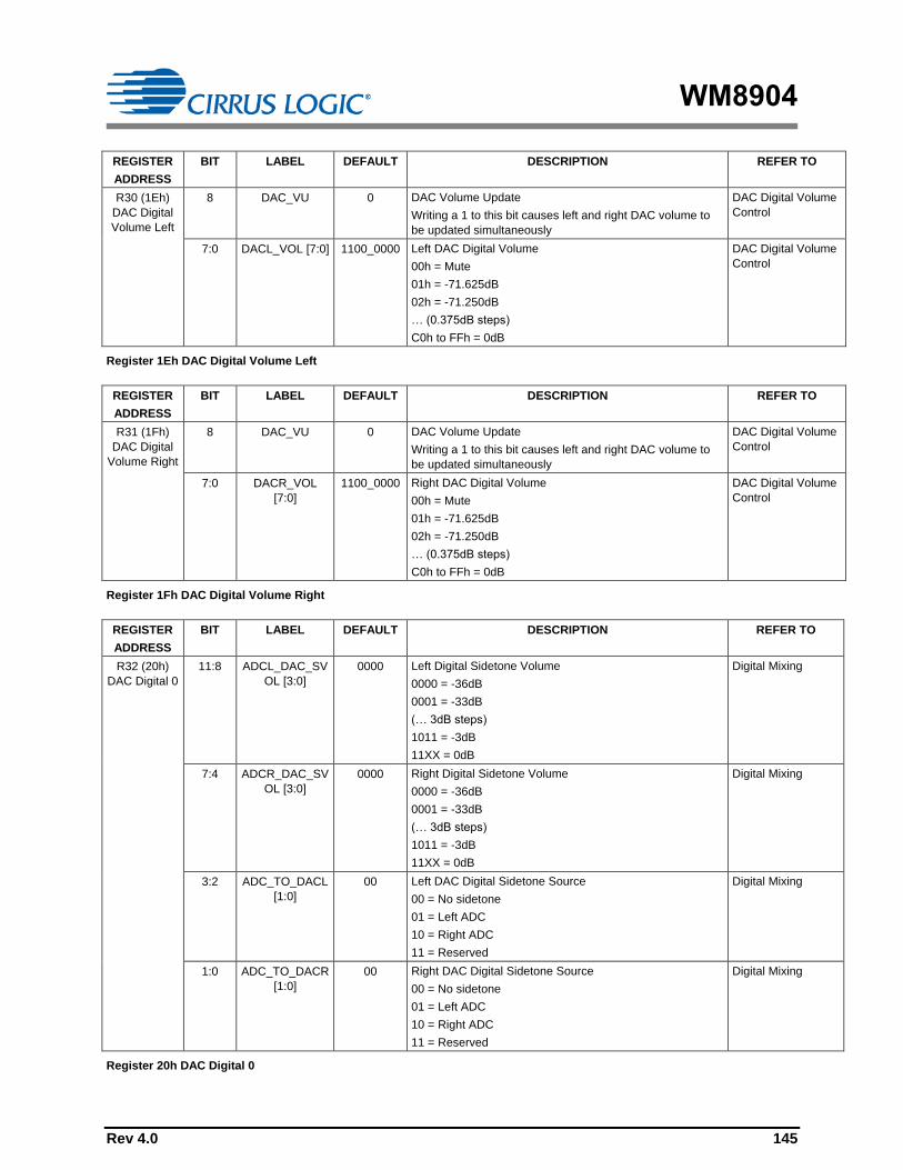
WM8904
Rev 4.0 145
REGISTER
ADDRESS
BIT LABEL DEFAULT DESCRIPTION REFER TO
R30 (1Eh)
DAC Digital
Volume Left
8 DAC_VU 0 DAC Volume Update
Writing a 1 to this bit causes left and right DAC volume to
be updated simultaneously
DAC Digital Volume
Control
7:0 DACL_VOL [7:0] 1100_0000 Left DAC Digital Volume
00h = Mute
01h = -71.625dB
02h = -71.250dB
… (0.375dB steps)
C0h to FFh = 0dB
DAC Digital Volume
Control
Register 1Eh DAC Digital Volume Left
REGISTER
ADDRESS
BIT LABEL DEFAULT DESCRIPTION REFER TO
R31 (1Fh)
DAC Digital
Volume Right
8 DAC_VU 0 DAC Volume Update
Writing a 1 to this bit causes left and right DAC volume to
be updated simultaneously
DAC Digital Volume
Control
7:0 DACR_VOL
[7:0]
1100_0000 Right DAC Digital Volume
00h = Mute
01h = -71.625dB
02h = -71.250dB
… (0.375dB steps)
C0h to FFh = 0dB
DAC Digital Volume
Control
Register 1Fh DAC Digital Volume Right
REGISTER
ADDRESS
BIT LABEL DEFAULT DESCRIPTION REFER TO
R32 (20h)
DAC Digital 0
11:8 ADCL_DAC_SV
OL [3:0]
0000 Left Digital Sidetone Volume
0000 = -36dB
0001 = -33dB
(… 3dB steps)
1011 = -3dB
11XX = 0dB
Digital Mixing
7:4 ADCR_DAC_SV
OL [3:0]
0000 Right Digital Sidetone Volume
0000 = -36dB
0001 = -33dB
(… 3dB steps)
1011 = -3dB
11XX = 0dB
Digital Mixing
3:2 ADC_TO_DACL
[1:0]
00 Left DAC Digital Sidetone Source
00 = No sidetone
01 = Left ADC
10 = Right ADC
11 = Reserved
Digital Mixing
1:0 ADC_TO_DACR
[1:0]
00 Right DAC Digital Sidetone Source
00 = No sidetone
01 = Left ADC
10 = Right ADC
11 = Reserved
Digital Mixing
Register 20h DAC Digital 0
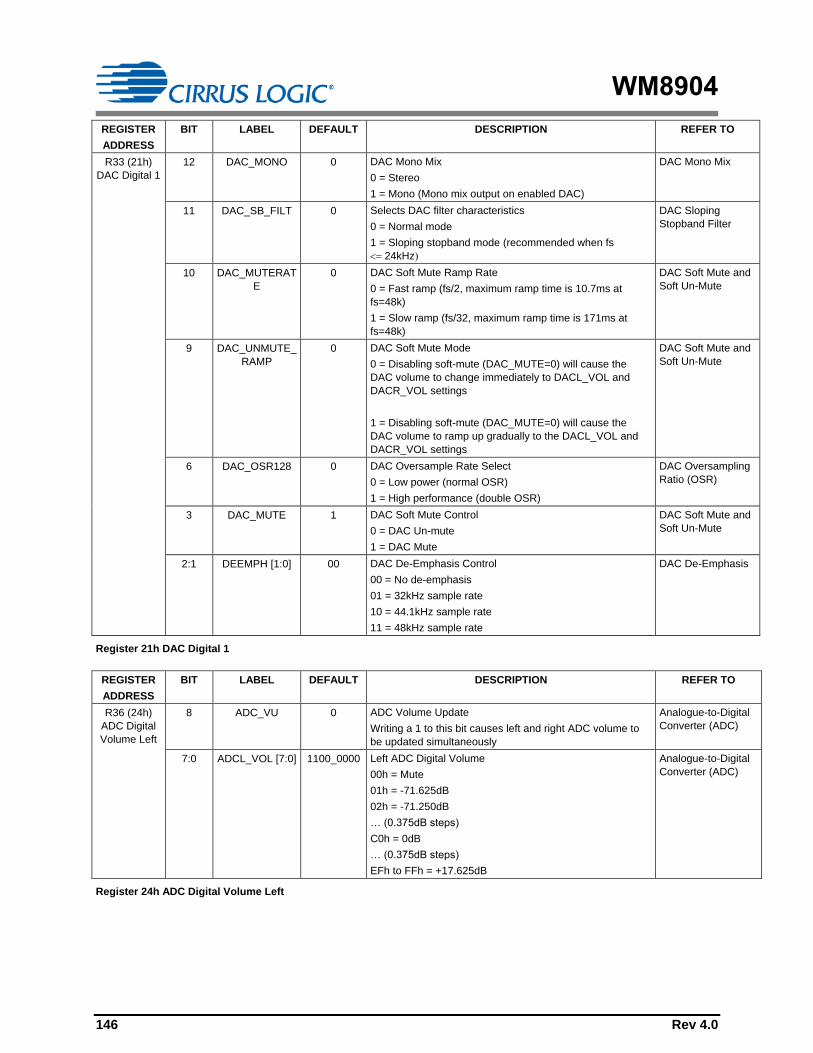
WM8904
146 Rev 4.0
REGISTER
ADDRESS
BIT LABEL DEFAULT DESCRIPTION REFER TO
R33 (21h)
DAC Digital 1
12 DAC_MONO 0 DAC Mono Mix
0 = Stereo
1 = Mono (Mono mix output on enabled DAC)
DAC Mono Mix
11 DAC_SB_FILT 0 Selects DAC filter characteristics
0 = Normal mode
1 = Sloping stopband mode (recommended when fs
24kHz
DAC Sloping
Stopband Filter
10 DAC_MUTERAT
E
0 DAC Soft Mute Ramp Rate
0 = Fast ramp (fs/2, maximum ramp time is 10.7ms at
fs=48k)
1 = Slow ramp (fs/32, maximum ramp time is 171ms at
fs=48k)
DAC Soft Mute and
Soft Un-Mute
9 DAC_UNMUTE_
RAMP
0 DAC Soft Mute Mode
0 = Disabling soft-mute (DAC_MUTE=0) will cause the
DAC volume to change immediately to DACL_VOL and
DACR_VOL settings
1 = Disabling soft-mute (DAC_MUTE=0) will cause the
DAC volume to ramp up gradually to the DACL_VOL and
DACR_VOL settings
DAC Soft Mute and
Soft Un-Mute
6 DAC_OSR128 0 DAC Oversample Rate Select
0 = Low power (normal OSR)
1 = High performance (double OSR)
DAC Oversampling
Ratio (OSR)
3 DAC_MUTE 1 DAC Soft Mute Control
0 = DAC Un-mute
1 = DAC Mute
DAC Soft Mute and
Soft Un-Mute
2:1 DEEMPH [1:0] 00 DAC De-Emphasis Control
00 = No de-emphasis
01 = 32kHz sample rate
10 = 44.1kHz sample rate
11 = 48kHz sample rate
DAC De-Emphasis
Register 21h DAC Digital 1
REGISTER
ADDRESS
BIT LABEL DEFAULT DESCRIPTION REFER TO
R36 (24h)
ADC Digital
Volume Left
8 ADC_VU 0 ADC Volume Update
Writing a 1 to this bit causes left and right ADC volume to
be updated simultaneously
Analogue-to-Digital
Converter (ADC)
7:0 ADCL_VOL [7:0] 1100_0000 Left ADC Digital Volume
00h = Mute
01h = -71.625dB
02h = -71.250dB
… (0.375dB steps)
C0h = 0dB
… (0.375dB steps)
EFh to FFh = +17.625dB
Analogue-to-Digital
Converter (ADC)
Register 24h ADC Digital Volume Left

WM8904
Rev 4.0 147
REGISTER
ADDRESS
BIT LABEL DEFAULT DESCRIPTION REFER TO
R37 (25h)
ADC Digital
Volume Right
8 ADC_VU 0 ADC Volume Update
Writing a 1 to this bit causes left and right ADC volume to
be updated simultaneously
Analogue-to-Digital
Converter (ADC)
7:0 ADCR_VOL
[7:0]
1100_0000 Right ADC Digital Volume
00h = Mute
01h = -71.625dB
02h = -71.250dB
… (0.375dB steps)
C0h = 0dB
… (0.375dB steps)
EFh to FFh = +17.625dB
Analogue-to-Digital
Converter (ADC)
Register 25h ADC Digital Volume Right
REGISTER
ADDRESS
BIT LABEL DEFAULT DESCRIPTION REFER TO
R38 (26h)
ADC Digital 0
6:5 ADC_HPF_CUT
[1:0]
00 ADC Digital High Pass Filter Cut-Off Frequency (fc)
00 = Hi-fi mode (fc=4Hz at fs=48kHz)
01 = Voice mode 1 (fc=127Hz at fs=16kHz)
10 = Voice mode 2 (fc=130Hz at fs=8kHz)
11 = Voice mode 3 (fc=267Hz at fs=8kHz)
(Note: fc scales with sample rate fs.)
Analogue-to-Digital
Converter (ADC)
4 ADC_HPF 1 ADC Digital High Pass Filter Enable
0 = disabled
1 = enabled
Analogue-to-Digital
Converter (ADC)
1 ADCL_DATINV 0 Left ADC Invert
0 = Left ADC output not inverted
1 = Left ADC output inverted
Analogue-to-Digital
Converter (ADC)
0 ADCR_DATINV 0 Right ADC Invert
0 = Right ADC output not inverted
1 = Right ADC output inverted
Analogue-to-Digital
Converter (ADC)
Register 26h ADC Digital 0
REGISTER
ADDRESS
BIT LABEL DEFAULT DESCRIPTION REFER TO
R39 (27h)
Digital
Microphone 0
12 DMIC_ENA 0 Enables Digital Microphone mode
0 = Audio DSP input is from ADC
1 = Audio DSP input is from digital microphone interface
When DMIC_ENA = 0, the Digital microphone clock
(DMICCLK) is held low.
Digital Microphone
Interface
11 DMIC_SRC 0 Selects Digital Microphone Data Input pin
0 = IN1L/DMICDAT1
1 = IN1R/DMICDAT2
Digital Microphone
Interface
Register 27h Digital Microphone 0

WM8904
148 Rev 4.0
REGISTER
ADDRESS
BIT LABEL DEFAULT DESCRIPTION REFER TO
R40 (28h)
DRC 0
15 DRC_ENA 0 DRC enable
1 = enabled
0 = disabled
Dynamic Range
Control (DRC)
14 DRC_DAC_PATH 0 DRC path select
0 = ADC path
1 = DAC path
Dynamic Range
Control (DRC)
12:11 DRC_GS_HYST_
LVL [1:0]
00 Gain smoothing hysteresis threshold
00 = Low
01 = Medium (recommended)
10 = High
11 = Reserved
Dynamic Range
Control (DRC)
10:6 DRC_STARTUP_
GAIN [4:0]
0_0110 Initial gain at DRC startup
00000 = -3dB
00001 = -2.5dB
00010 = -2dB
00011 = -1.5dB
00100 = -1dB
00101 = -0.5dB
00110 = 0dB (default)
00111 = 0.5dB
01000 = 1dB
01001 = 1.5dB
01010 = 2dB
01011 = 2.5dB
01100 = 3dB
01101 = 3.5dB
01110 = 4dB
01111 = 4.5dB
10000 = 5dB
10001 = 5.5dB
10010 = 6dB
10011 to 11111 = Reserved
Dynamic Range
Control (DRC)
5 DRC_FF_DELAY 1 Feed-forward delay for anti-clip feature
0 = 5 samples
1 = 9 samples
Time delay can be calculated as 5/fs or 9/ fs, where fs is
the sample rate.
Dynamic Range
Control (DRC)
3 DRC_GS_ENA 1 Gain smoothing enable
0 = disabled
1 = enabled
Dynamic Range
Control (DRC)
2 DRC_QR 1 Quick release enable
0 = disabled
1 = enabled
Dynamic Range
Control (DRC)
1 DRC_ANTICLIP 1 Anti-clip enable
0 = disabled
1 = enabled
Dynamic Range
Control (DRC)
0 DRC_GS_HYST 1 Gain smoothing hysteresis enable
0 = disabled
1 = enabled
Dynamic Range
Control (DRC)
Register 28h DRC 0

WM8904
Rev 4.0 149
REGISTER
ADDRESS
BIT LABEL DEFAULT DESCRIPTION REFER TO
R41 (29h)
DRC 1
15:12 DRC_ATK [3:0] 0011 Gain attack rate (seconds/6dB)
0000 = Reserved
0001 = 182µs
0010 = 363µs
0011 = 726µs (default)
0100 = 1.45ms
0101 = 2.9ms
0110 = 5.8ms
0111 = 11.6ms
1000 = 23.2ms
1001 = 46.4ms
1010 = 92.8ms
1011-1111 = Reserved
Dynamic Range
Control (DRC)
11:8 DRC_DCY [3:0] 0010 Gain decay rate (seconds/6dB)
0000 = 186ms
0001 = 372ms
0010 = 743ms (default)
0011 = 1.49s
0100 = 2.97s
0101 = 5.94s
0110 = 11.89s
0111 = 23.78s
1000 = 47.56s
1001-1111 = Reserved
Dynamic Range
Control (DRC)
7:6 DRC_QR_THR
[1:0]
01 Quick release crest factor threshold
00 = 12dB
01 = 18dB (default)
10 = 24dB
11 = 30dB
Dynamic Range
Control (DRC)
5:4 DRC_QR_DCY
[1:0]
00 Quick release decay rate (seconds/6dB)
00 = 0.725ms (default)
01 = 1.45ms
10 = 5.8ms
11 = Reserved
Dynamic Range
Control (DRC)
3:2 DRC_MINGAIN
[1:0]
10 Minimum gain the DRC can use to attenuate audio
signals
00 = 0dB (default)
01 = -6dB
10 = -12dB
11 = -18dB
Dynamic Range
Control (DRC)
1:0 DRC_MAXGAIN
[1:0]
00 Maximum gain the DRC can use to boost audio signals
00 = 12dB
01 = 18dB (default)
10 = 24dB
11 = 36dB
Dynamic Range
Control (DRC)
Register 29h DRC 1

WM8904
150 Rev 4.0
REGISTER
ADDRESS
BIT LABEL DEFAULT DESCRIPTION REFER TO
R42 (2Ah)
DRC 2
5:3 DRC_HI_COMP
[2:0]
000 Compressor slope (upper region)
000 = 1 (no compression)
001 = 1/2
010 = 1/4
011 = 1/8
100 = 1/16
101 = 0
110 to 111 = Reserved
Dynamic Range
Control (DRC)
2:0 DRC_LO_COM
P [2:0]
000 Compressor slope (lower region)
000 = 1 (no compression)
001 = 1/2
010 = 1/4
011 = 1/8
100 = 0
101 to 111 = Reserved
Dynamic Range
Control (DRC)
Register 2Ah DRC 2
REGISTER
ADDRESS
BIT LABEL DEFAULT DESCRIPTION REFER TO
R43 (2Bh)
DRC 3
10:5 DRC_KNEE_IP
[5:0]
00_0000 Input signal at the Compressor 'knee'.
000000 = 0dB
000001 = -0.75dB
000010 = -1.5dB
… (-0.75dB steps)
111100 = -45dB
111101 to 111111 = Reserved
Dynamic Range
Control (DRC)
4:0 DRC_KNEE_OP
[4:0]
0_0000 Output signal at the Compressor 'knee'.
00000 = 0dB
00001 = -0.75dB
00010 = -1.5dB
… (-0.75dB steps)
11110 = -22.5dB
11111 = Reserved
Dynamic Range
Control (DRC)
Register 2Bh DRC 3

WM8904
Rev 4.0 151
REGISTER
ADDRESS
BIT LABEL DEFAULT DESCRIPTION REFER TO
R44 (2Ch)
Analogue Left
Input 0
7 LINMUTE 1 Left Input PGA Mute
0 = not muted
1 = muted
Input PGA Gain
Control
4:0 LIN_VOL [4:0] 0_0101 Left Input PGA Volume
If L_MODE = 00 (Single ended)
OR L_MODE = 01 (Differential Line)
00000 = -1.5 dB
00001 = -1.3 dB
00010 = -1.0 dB
00011 = -0.7 dB
00100 = -0.3 dB
00101 = +0.0 dB (default)
00110 = +0.3 dB
00111 = +0.7 dB
01000 = +1.0 dB
01001 = +1.4 dB
01010 = +1.8 dB
01011 = +2.3 dB
01100 = +2.7 dB
01101 = +3.2 dB
01110 = +3.7 dB
01111 = +4.2 dB
10000 = +4.8 dB
10001 = +5.4 dB
10010 = +6.0 dB
10011 = +6.7 dB
10100 = +7.5 dB
10101 = +8.3 dB
10110 = +9.2 dB
10111 = +10.2 dB
11000 = +11.4 dB
11001 = +12.7 dB
11010 = +14.3 dB
11011 = +16.2 dB
11100 = +19.2 dB
11101 = +22.3 dB
11110 = +25.2 dB
11111 = +28.3 dB
If L_MODE = 10 (Differential MIC)
00000 = Reserved
00001 = +12 dB
00010 = +15 dB
00011 = +18 dB
00100 = +21 dB
00101 = +24 dB (default)
00110 = +27 dB
00111 to 11111 = +30 dB
Input PGA Gain
Control
Register 2Ch Analogue Left Input 0

WM8904
152 Rev 4.0
REGISTER
ADDRESS
BIT LABEL DEFAULT DESCRIPTION REFER TO
R45 (2Dh)
Analogue
Right Input 0
7 RINMUTE 1 Right Input PGA Mute
0 = not muted
1 = muted
Input PGA Gain
Control
4:0 RIN_VOL [4:0] 0_0101 Right Input PGA Volume
If R_MODE = 00 (Single ended)
OR R_MODE = 01 (Differential Line)
00000 = -1.5 dB
00001 = -1.3 dB
00010 = -1.0 dB
00011 = -0.7 dB
00100 = -0.3 dB
00101 = +0.0 dB (default)
00110 = +0.3 dB
00111 = +0.7 dB
01000 = +1.0 dB
01001 = +1.4 dB
01010 = +1.8 dB
01011 = +2.3 dB
01100 = +2.7 dB
01101 = +3.2 dB
01110 = +3.7 dB
01111 = +4.2 dB
10000 = +4.8 dB
10001 = +5.4 dB
10010 = +6.0 dB
10011 = +6.7 dB
10100 = +7.5 dB
10101 = +8.3 dB
10110 = +9.2 dB
10111 = +10.2 dB
11000 = +11.4 dB
11001 = +12.7 dB
11010 = +14.3 dB
11011 = +16.2 dB
11100 = +19.2 dB
11101 = +22.3 dB
11110 = +25.2 dB
11111 = +28.3 dB
If R_MODE = 10 (Differential MIC)
00000 = Reserved
00001 = +12 dB
00010 = +15 dB
00011 = +18 dB
00100 = +21 dB
00101 = +24 dB (default)
00110 = +27 dB
00111 to 11111 = +30 dB
Input PGA Gain
Control
Register 2Dh Analogue Right Input 0

WM8904
Rev 4.0 153
REGISTER
ADDRESS
BIT LABEL DEFAULT DESCRIPTION REFER TO
R46 (2Eh)
Analogue Left
Input 1
6 INL_CM_ENA 1 Left Input PGA Common Mode Rejection enable
0 = Disabled
1 = Enabled
(only available for L_MODE=01 – Differential Line)
Input PGA Common
Mode Amplifier
5:4 L_IP_SEL_N
[1:0]
00 In Single-Ended or Differential Line Modes, this field selects
the input pin for the inverting side of the left input path.
In Differential Mic Mode, this field selects the input pin for
the non-inverting side of the left input path.
00 = IN1L
01 = IN2L
1X = IN3L
Analogue Input
Signal Path
3:2 L_IP_SEL_P
[1:0]
01 In Single-Ended or Differential Line Modes, this field selects
the input pin for the non-inverting side of the left input path.
In Differential Mic Mode, this field selects the input pin for
the inverting side of the left input path.
00 = IN1L
01 = IN2L
1X = IN3L
Analogue Input
Signal Path
1:0 L_MODE [1:0] 00 Sets the mode for the left analogue input:
00 = Single-Ended
01 = Differential Line
10 = Differential MIC
11 = Reserved
Analogue Input
Signal Path
Register 2Eh Analogue Left Input 1
REGISTER
ADDRESS
BIT LABEL DEFAULT DESCRIPTION REFER TO
R47 (2Fh)
Analogue
Right Input 1
6 INR_CM_ENA 1 Right Input PGA Common Mode Rejection enable
0 = Disabled
1 = Enabled
(only available for R_MODE=01 – Differential Line)
Input PGA Common
Mode Amplifier
5:4 R_IP_SEL_N
[1:0]
00 In Single-Ended or Differential Line Modes, this field selects
the input pin for the inverting side of the right input path.
In Differential Mic Mode, this field selects the input pin for
the non-inverting side of the right input path.
00 = IN1R
01 = IN2R
1X = IN3R
Analogue Input
Signal Path
3:2 R_IP_SEL_P
[1:0]
01 In Single-Ended or Differential Line Modes, this field selects
the input pin for the non-inverting side of the right input
path.
In Differential Mic Mode, this field selects the input pin for
the inverting side of the right input path.
00 = IN1R
01 = IN2R
1X = IN3R
Analogue Input
Signal Path
1:0 R_MODE [1:0] 00 Sets the mode for the right analogue input:
00 = Single-Ended
01 = Differential Line
10 = Differential MIC
11 = Reserved
Analogue Input
Signal Path
Register 2Fh Analogue Right Input 1

WM8904
154 Rev 4.0
REGISTER
ADDRESS
BIT LABEL DEFAULT DESCRIPTION REFER TO
R57 (39h)
Analogue
OUT1 Left
8 HPOUTL_MUTE 0 Left Headphone Output Mute
0 = Un-mute
1 = Mute
Output Volume
Control
7 HPOUT_VU 0 Headphone Output Volume Update
Writing a 1 to this bit will update HPOUTL and HPOUTR
volumes simultaneously.
Output Volume
Control
6 HPOUTLZC 0 Left Headphone Output Zero Cross Enable
0 = disabled
1 = enabled
Output Volume
Control
5:0 HPOUTL_VOL
[5:0]
10_1101 Left Headphone Output Volume
000000 = -57dB
000001 = -56dB
(… 1dB steps)
111001 = 0dB
(… 1dB steps)
111110 = +5dB
111111 = +6dB
Output Volume
Control
Register 39h Analogue OUT1 Left
REGISTER
ADDRESS
BIT LABEL DEFAULT DESCRIPTION REFER TO
R58 (3Ah)
Analogue
OUT1 Right
8 HPOUTR_MUT
E
0 Right Headphone Output Mute
0 = Un-mute
1 = Mute
Output Volume
Control
7 HPOUT_VU 0 Headphone Output Volume Update
Writing a 1 to this bit will update HPOUTL and HPOUTR
volumes simultaneously.
Output Volume
Control
6 HPOUTRZC 0 Right Headphone Output Zero Cross Enable
0 = disabled
1 = enabled
Output Volume
Control
5:0 HPOUTR_VOL
[5:0]
10_1101 Right Headphone Output Volume
000000 = -57dB
000001 = -56dB
(… 1dB steps)
111001 = 0dB
(… 1dB steps)
111110 = +5dB
111111 = +6dB
Output Volume
Control
Register 3Ah Analogue OUT1 Right

WM8904
Rev 4.0 155
REGISTER
ADDRESS
BIT LABEL DEFAULT DESCRIPTION REFER TO
R59 (3Bh)
Analogue
OUT2 Left
8 LINEOUTL_MU
TE
0 Left Line Output Mute
0 = Un-mute
1 = Mute
Output Volume
Control
7 LINEOUT_VU 0 Line Output Volume Update
Writing a 1 to this bit will update LINEOUTL and
LINEOUTR volumes simultaneously.
Output Volume
Control
6 LINEOUTLZC 0 Left Line Output Zero Cross Enable
0 = disabled
1 = enabled
Output Volume
Control
5:0 LINEOUTL_VOL
[5:0]
11_1001 Left Line Output Volume
000000 = -57dB
000001 = -56dB
(… 1dB steps)
111001 = 0dB
(… 1dB steps)
111110 = +5dB
111111 = +6dB
Output Volume
Control
Register 3Bh Analogue OUT2 Left
REGISTER
ADDRESS
BIT LABEL DEFAULT DESCRIPTION REFER TO
R60 (3Ch)
Analogue
OUT2 Right
8 LINEOUTR_MU
TE
0 Right Line Output Mute
0 = Un-mute
1 = Mute
Output Volume
Control
7 LINEOUT_VU 0 Line Output Volume Update
Writing a 1 to this bit will update LINEOUTL and
LINEOUTR volumes simultaneously.
Output Volume
Control
6 LINEOUTRZC 0 Right Line Output Zero Cross Enable
0 = disabled
1 = enabled
Output Volume
Control
5:0 LINEOUTR_VO
L [5:0]
11_1001 Right Line Output Volume
000000 = -57dB
000001 = -56dB
(… 1dB steps)
111001 = 0dB
(… 1dB steps)
111110 = +5dB
111111 = +6dB
Output Volume
Control
Register 3Ch Analogue OUT2 Right

WM8904
156 Rev 4.0
REGISTER
ADDRESS
BIT LABEL DEFAULT DESCRIPTION REFER TO
R61 (3Dh)
Analogue
OUT12 ZC
3 HPL_BYP_ENA 0 Selects input for left headphone output MUX
0 = Left DAC
1 = Left input PGA (Analogue bypass)
Output Signal Paths
Enable
2 HPR_BYP_ENA 0 Selects input for right headphone output MUX
0 = Right DAC
1 = Right input PGA (Analogue bypass)
Output Signal Paths
Enable
1 LINEOUTL_BYP
_ENA
0 Selects input for left line output MUX
0 = Left DAC
1 = Left input PGA (Analogue bypass)
Output Signal Paths
Enable
0 LINEOUTR_BY
P_ENA
0 Selects input for right line output MUX
0 = Right DAC
1 = Right input PGA (Analogue bypass)
Output Signal Paths
Enable
Register 3Dh Analogue OUT12 ZC
REGISTER
ADDRESS
BIT LABEL DEFAULT DESCRIPTION REFER TO
R67 (43h) DC
Servo 0
3 DCS_ENA_CHA
N_3
0 DC Servo enable for LINEOUTR
0 = disabled
1 = enabled
DC Servo
2 DCS_ENA_CHA
N_2
0 DC Servo enable for LINEOUTL
0 = disabled
1 = enabled
DC Servo
1 DCS_ENA_CHA
N_1
0 DC Servo enable for HPOUTR
0 = disabled
1 = enabled
DC Servo
0 DCS_ENA_CHA
N_0
0 DC Servo enable for HPOUTL
0 = disabled
1 = enabled
DC Servo
Register 43h DC Servo 0
REGISTER
ADDRESS
BIT LABEL DEFAULT DESCRIPTION REFER TO
R68 (44h) DC
Servo 1
15 DCS_TRIG_SIN
GLE_3
0 Writing 1 to this bit selects a single DC offset correction for
LINEOUTR.
In readback, a value of 1 indicates that the DC Servo single
correction is in progress.
DC Servo
14 DCS_TRIG_SIN
GLE_2
0 Writing 1 to this bit selects a single DC offset correction for
LINEOUTL.
In readback, a value of 1 indicates that the DC Servo single
correction is in progress.
DC Servo
13 DCS_TRIG_SIN
GLE_1
0 Writing 1 to this bit selects a single DC offset correction for
HPOUTR.
In readback, a value of 1 indicates that the DC Servo single
correction is in progress.
DC Servo
12 DCS_TRIG_SIN
GLE_0
0 Writing 1 to this bit selects a single DC offset correction for
HPOUTL.
In readback, a value of 1 indicates that the DC Servo single
correction is in progress.
DC Servo
11 DCS_TRIG_SE
RIES_3
0 Writing 1 to this bit selects a series of DC offset corrections
for LINEOUTR.
In readback, a value of 1 indicates that the DC Servo DAC
Write correction is in progress.
DC Servo

WM8904
Rev 4.0 157
REGISTER
ADDRESS
BIT LABEL DEFAULT DESCRIPTION REFER TO
10 DCS_TRIG_SE
RIES_2
0 Writing 1 to this bit selects a series of DC offset corrections
for LINEOUTL.
In readback, a value of 1 indicates that the DC Servo DAC
Write correction is in progress.
DC Servo
9 DCS_TRIG_SE
RIES_1
0 Writing 1 to this bit selects a series of DC offset corrections
for HPOUTR.
In readback, a value of 1 indicates that the DC Servo DAC
Write correction is in progress.
DC Servo
8 DCS_TRIG_SE
RIES_0
0 Writing 1 to this bit selects a series of DC offset corrections
for HPOUTL.
In readback, a value of 1 indicates that the DC Servo DAC
Write correction is in progress.
DC Servo
7 DCS_TRIG_STA
RTUP_3
0 Writing 1 to this bit selects Start-Up DC Servo mode for
LINEOUTR.
In readback, a value of 1 indicates that the DC Servo Start-
Up correction is in progress.
DC Servo
6 DCS_TRIG_STA
RTUP_2
0 Writing 1 to this bit selects Start-Up DC Servo mode for
LINEOUTL.
In readback, a value of 1 indicates that the DC Servo Start-
Up correction is in progress.
DC Servo
5 DCS_TRIG_STA
RTUP_1
0 Writing 1 to this bit selects Start-Up DC Servo mode for
HPOUTR.
In readback, a value of 1 indicates that the DC Servo Start-
Up correction is in progress.
DC Servo
4 DCS_TRIG_STA
RTUP_0
0 Writing 1 to this bit selects Start-Up DC Servo mode for
HPOUTL.
In readback, a value of 1 indicates that the DC Servo Start-
Up correction is in progress.
DC Servo
3 DCS_TRIG_DA
C_WR_3
0 Writing 1 to this bit selects DAC Write DC Servo mode for
LINEOUTR.
In readback, a value of 1 indicates that the DC Servo DAC
Write correction is in progress.
DC Servo
2 DCS_TRIG_DA
C_WR_2
0 Writing 1 to this bit selects DAC Write DC Servo mode for
LINEOUTL.
In readback, a value of 1 indicates that the DC Servo DAC
Write correction is in progress.
DC Servo
1 DCS_TRIG_DA
C_WR_1
0 Writing 1 to this bit selects DAC Write DC Servo mode for
HPOUTR.
In readback, a value of 1 indicates that the DC Servo DAC
Write correction is in progress.
DC Servo
0 DCS_TRIG_DA
C_WR_0
0 Writing 1 to this bit selects DAC Write DC Servo mode for
HPOUTL.
In readback, a value of 1 indicates that the DC Servo DAC
Write correction is in progress.
DC Servo
Register 44h DC Servo 1

WM8904
158 Rev 4.0
REGISTER
ADDRESS
BIT LABEL DEFAULT DESCRIPTION REFER TO
R69 (45h) DC
Servo 2
11:8 DCS_TIMER_PE
RIOD_23 [3:0]
1010 Time between periodic updates for
LINEOUTL/LINEOUTR. Time is calculated as 0.256s x
(2^PERIOD)
0000 = Off
0001 = 0.52s
1010 = 266s (4min 26s)
1111 = 8519s (2hr 22s)
DC Servo
3:0 DCS_TIMER_PE
RIOD_01 [3:0]
1010 Time between periodic updates for HPOUTL/HPOUTR.
Time is calculated as 0.256s x (2^PERIOD)
0000 = Off
0001 = 0.52s
1010 = 266s (4min 26s)
1111 = 8519s (2hr 22s)
DC Servo
Register 45h DC Servo 2
REGISTER
ADDRESS
BIT LABEL DEFAULT DESCRIPTION REFER TO
R71 (47h) DC
Servo 4
6:0 DCS_SERIES_N
O_23 [6:0]
010_1010 Number of DC Servo updates to perform in a series
event for LINEOUTL/LINEOUTR.
0 = 1 updates
1 = 2 updates
...
127 = 128 updates
DC Servo
Register 47h DC Servo 4
REGISTER
ADDRESS
BIT LABEL DEFAULT DESCRIPTION REFER TO
R72 (48h) DC
Servo 5
6:0 DCS_SERIES_N
O_01 [6:0]
010_1010 Number of DC Servo updates to perform in a series
event for HPOUTL/HPOUTR.
0 = 1 updates
1 = 2 updates
...
127 = 128 updates
DC Servo
Register 48h DC Servo 5
REGISTER
ADDRESS
BIT LABEL DEFAULT DESCRIPTION REFER TO
R73 (49h) DC
Servo 6
7:0 DCS_DAC_WR_
VAL_3 [7:0]
0000_0000 DC Offset value for LINEOUTR in DAC Write DC Servo
mode in two's complement format.
In readback, the current DC offset value is returned in
two's complement format.
Two’s complement format:
LSB is 0.25mV.
Range is +/-32mV
DC Servo
Register 49h DC Servo 6

WM8904
Rev 4.0 159
REGISTER
ADDRESS
BIT LABEL DEFAULT DESCRIPTION REFER TO
R74 (4Ah)
DC Servo 7
7:0 DCS_DAC_WR_
VAL_2 [7:0]
0000_0000 DC Offset value for LINEOUTL in DAC Write DC Servo
mode in two's complement format.
In readback, the current DC offset value is returned in
two's complement format.
Two’s complement format:
LSB is 0.25mV.
Range is +/-32mV
DC Servo
Register 4Ah DC Servo 7
REGISTER
ADDRESS
BIT LABEL DEFAULT DESCRIPTION REFER TO
R75 (4Bh)
DC Servo 8
7:0 DCS_DAC_WR_
VAL_1 [7:0]
0000_0000 DC Offset value for HPOUTR in DAC Write DC Servo
mode in two's complement format.
In readback, the current DC offset value is returned in
two's complement format.
Two’s complement format:
LSB is 0.25mV.
Range is +/-32mV
DC Servo
Register 4Bh DC Servo 8
REGISTER
ADDRESS
BIT LABEL DEFAULT DESCRIPTION REFER TO
R76 (4Ch)
DC Servo 9
7:0 DCS_DAC_WR_
VAL_0 [7:0]
0000_0000 DC Offset value for HPOUTL in DAC Write DC Servo
mode in two's complement format.
In readback, the current DC offset value is returned in
two's complement format.
Two’s complement format:
LSB is 0.25mV.
Range is +/-32mV
DC Servo
Register 4Ch DC Servo 9
REGISTER
ADDRESS
BIT LABEL DEFAULT DESCRIPTION REFER TO
R77 (4Dh)
DC Servo
Readback 0
11:8 DCS_CAL_COMP
LETE [3:0]
0000 DC Servo Complete status
[3] - LINEOUTR
[2] - LINEOUTL
[1] - HPOUTR
[0] - HPOUTL
0 = DAC Write or Start-Up DC Servo mode not
completed.
1 = DAC Write or Start-Up DC Servo mode complete.
DC Servo

WM8904
160 Rev 4.0
REGISTER
ADDRESS
BIT LABEL DEFAULT DESCRIPTION REFER TO
7:4 DCS_DAC_WR_C
OMPLETE [3:0]
0000 DC Servo DAC Write status
[3] - LINEOUTR
[2] - LINEOUTL
[1] - HPOUTR
[0] - HPOUTL
0 = DAC Write DC Servo mode not completed.
1 = DAC Write DC Servo mode complete.
DC Servo
3:0 DCS_STARTUP_
COMPLETE [3:0]
0000 DC Servo Start-Up status
[3] - LINEOUTR
[2] - LINEOUTL
[1] - HPOUTR
[0] - HPOUTL
0 = Start-Up DC Servo mode not completed..
1 = Start-Up DC Servo mode complete.
DC Servo
Register 4Dh DC Servo Readback 0
REGISTER
ADDRESS
BIT LABEL DEFAULT DESCRIPTION REFER TO
R90 (5Ah)
Analogue HP
0
7 HPL_RMV_SHOR
T
0 Removes HPOUTL short
0 = HPOUTL short enabled
1 = HPOUTL short removed
For normal operation, this bit should be set as the final
step of the HPL Enable sequence.
Pop Suppression
Control
6 HPL_ENA_OUTP 0 Enables HPOUTL output stage
0 = Disabled
1 = Enabled
For normal operation, this bit should be set to 1 after the
DC offset cancellation has been scheduled.
Pop Suppression
Control
5 HPL_ENA_DLY 0 Enables HPOUTL intermediate stage
0 = Disabled
1 = Enabled
For normal operation, this bit should be set to 1 after the
output signal path has been configured, and before DC
offset cancellation is scheduled. This bit should be set
with at least 20us delay after HPL_ENA.
Pop Suppression
Control
4 HPL_ENA 0 Enables HPOUTL input stage
0 = Disabled
1 = Enabled
For normal operation, this bit should be set as the first
step of the HPL Enable sequence.
Pop Suppression
Control
3 HPR_RMV_SHO
RT
0 Removes HPOUTR short
0 = HPOUTR short enabled
1 = HPOUTR short removed
For normal operation, this bit should be set as the final
step of the HPR Enable sequence.
Pop Suppression
Control
2 HPR_ENA_OUTP 0 Enables HPOUTR output stage
0 = Disabled
1 = Enabled
For normal operation, this bit should be set to 1 after the
DC offset cancellation has been scheduled.
Pop Suppression
Control
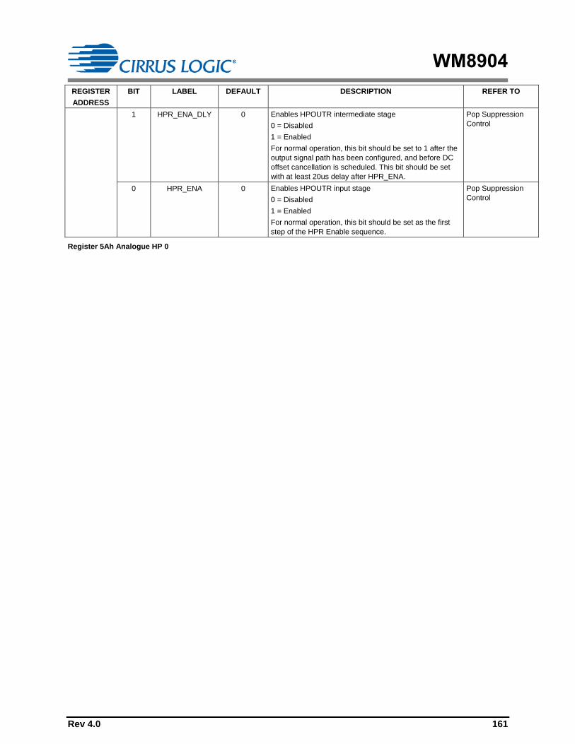
WM8904
Rev 4.0 161
REGISTER
ADDRESS
BIT LABEL DEFAULT DESCRIPTION REFER TO
1 HPR_ENA_DLY 0 Enables HPOUTR intermediate stage
0 = Disabled
1 = Enabled
For normal operation, this bit should be set to 1 after the
output signal path has been configured, and before DC
offset cancellation is scheduled. This bit should be set
with at least 20us delay after HPR_ENA.
Pop Suppression
Control
0 HPR_ENA 0 Enables HPOUTR input stage
0 = Disabled
1 = Enabled
For normal operation, this bit should be set as the first
step of the HPR Enable sequence.
Pop Suppression
Control
Register 5Ah Analogue HP 0

WM8904
162 Rev 4.0
REGISTER
ADDRESS
BIT LABEL DEFAULT DESCRIPTION REFER TO
R94 (5Eh)
Analogue
Lineout 0
7 LINEOUTL_RMV
_SHORT
0 Removes LINEOUTL short
0 = LINEOUTL short enabled
1 = LINEOUTL short removed
For normal operation, this bit should be set as the final
step of the LINEOUTL Enable sequence.
Pop Suppression
Control
6 LINEOUTL_ENA_
OUTP
0 Enables LINEOUTL output stage
0 = Disabled
1 = Enabled
For normal operation, this bit should be set to 1 after the
DC offset cancellation has been scheduled.
Pop Suppression
Control
5 LINEOUTL_ENA_
DLY
0 Enables LINEOUTL intermediate stage
0 = Disabled
1 = Enabled
For normal operation, this bit should be set to 1 after the
output signal path has been configured, and before DC
offset cancellation is scheduled. This bit should be set
with at least 20us delay after LINEOUTL_ENA.
Pop Suppression
Control
4 LINEOUTL_ENA 0 Enables LINEOUTL input stage
0 = Disabled
1 = Enabled
For normal operation, this bit should be set as the first
step of the LINEOUTL Enable sequence.
Pop Suppression
Control
3 LINEOUTR_RMV
_SHORT
0 Removes LINEOUTR short
0 = LINEOUTR short enabled
1 = LINEOUTR short removed
For normal operation, this bit should be set as the final
step of the LINEOUTR Enable sequence.
Pop Suppression
Control
2 LINEOUTR_ENA
_OUTP
0 Enables LINEOUTR output stage
0 = Disabled
1 = Enabled
For normal operation, this bit should be set to 1 after the
DC offset cancellation has been scheduled.
Pop Suppression
Control
1 LINEOUTR_ENA
_DLY
0 Enables LINEOUTR intermediate stage
0 = Disabled
1 = Enabled
For normal operation, this bit should be set to 1 after the
output signal path has been configured, and before DC
offset cancellation is scheduled. This bit should be set
with at least 20us delay after LINEOUTR_ENA.
Pop Suppression
Control
0 LINEOUTR_ENA 0 Enables LINEOUTR input stage
0 = Disabled
1 = Enabled
For normal operation, this bit should be set as the first
step of the LINEOUTR Enable sequence.
Pop Suppression
Control
Register 5Eh Analogue Lineout 0

WM8904
Rev 4.0 163
REGISTER
ADDRESS
BIT LABEL DEFAULT DESCRIPTION REFER TO
R98 (62h)
Charge Pump
0
0 CP_ENA 0 Enable charge-pump digits
0 = disable
1 = enable
Charge Pump
Register 62h Charge Pump 0
REGISTER
ADDRESS
BIT LABEL DEFAULT DESCRIPTION REFER TO
R104 (68h)
Class W
0 CP_DYN_PWR 0 Enable dynamic charge pump power control
0 = Charge pump controlled by volume register settings
(Class G)
1 = Charge pump controlled by real-time audio level
(Class W)
Class W is recommended for lowest power consumption.
Charge Pump
Register 68h Class W
REGISTER
ADDRESS
BIT LABEL DEFAULT DESCRIPTION REFER TO
R108 (6Ch)
Write
Sequencer 0
8 WSEQ_ENA 0 Write Sequencer Enable.
0 = Disabled
1 = Enabled
Control Write
Sequencer
4:0 WSEQ_WRITE_I
NDEX [4:0]
0_0000 Sequence Write Index. This is the memory location to
which any updates to R109 and R110 will be copied.
0 to 31 = RAM addresses
Control Write
Sequencer
Register 6Ch Write Sequencer 0
REGISTER
ADDRESS
BIT LABEL DEFAULT DESCRIPTION REFER TO
R109 (6Dh)
Write
Sequencer 1
14:12 WSEQ_DATA_WI
DTH [2:0]
000 Width of the data block written in this sequence step.
000 = 1 bit
001 = 2 bits
010 = 3 bits
011 = 4 bits
100 = 5 bits
101 = 6 bits
110 = 7 bits
111 = 8 bits
Control Write
Sequencer
11:8 WSEQ_DATA_ST
ART [3:0]
0000 Bit position of the LSB of the data block written in this
sequence step.
0000 = Bit 0
…
1111 = Bit 15
Control Write
Sequencer
7:0 WSEQ_ADDR
[7:0]
0000_0000 Control Register Address to be written to in this
sequence step.
Control Write
Sequencer
Register 6Dh Write Sequencer 1

WM8904
164 Rev 4.0
REGISTER
ADDRESS
BIT LABEL DEFAULT DESCRIPTION REFER TO
R110 (6Eh)
Write
Sequencer 2
14 WSEQ_EOS 0 End of Sequence flag. This bit indicates whether the
Control Write Sequencer should stop after executing this
step.
0 = Not end of sequence
1 = End of sequence (Stop the sequencer after this
step).
Control Write
Sequencer
11:8 WSEQ_DELAY
[3:0]
0000 Time delay after executing this step.
Total delay time per step (including execution)=
62.5µs × (2^WSEQ_DELAY + 8)
Control Write
Sequencer
7:0 WSEQ_DATA
[7:0]
0000_0000 Data to be written in this sequence step. When the data
width is less than 8 bits, then one or more of the MSBs
of WSEQ_DATA are ignored. It is recommended that
unused bits be set to 0.
Control Write
Sequencer
Register 6Eh Write Sequencer 2
REGISTER
ADDRESS
BIT LABEL DEFAULT DESCRIPTION REFER TO
R111 (6Fh)
Write
Sequencer 3
9 WSEQ_ABORT 0 Writing a 1 to this bit aborts the current sequence and
returns control of the device back to the serial control
interface.
Control Write
Sequencer
8 WSEQ_START 0 Writing a 1 to this bit starts the write sequencer at the
memory location indicated by the WSEQ_START_INDEX
field. The sequence continues until it reaches an “End of
sequence” flag. At the end of the sequence, this bit will
be reset by the Write Sequencer.
Control Write
Sequencer
5:0 WSEQ_START_I
NDEX [5:0]
00_0000 Sequence Start Index. This is the memory location of the
first command in the selected sequence.
0 to 31 = RAM addresses
32 to 48 = ROM addresses
49 to 63 = Reserved
Control Write
Sequencer
Register 6Fh Write Sequencer 3
REGISTER
ADDRESS
BIT LABEL DEFAULT DESCRIPTION REFER TO
R112 (70h)
Write
Sequencer 4
9:4 WSEQ_CURREN
T_INDEX [5:0]
00_0000 Sequence Current Index (read only):
This is the location of the most recently accessed
command in the write sequencer memory.
Control Write
Sequencer
0 WSEQ_BUSY 0 Sequencer Busy flag (read only):
0 = Sequencer idle
1 = Sequencer busy
Note: it is not possible to write to control registers via the
control interface while the Sequencer is Busy.
Control Write
Sequencer
Register 70h Write Sequencer 4

WM8904
Rev 4.0 165
REGISTER
ADDRESS
BIT LABEL DEFAULT DESCRIPTION REFER TO
R116 (74h)
FLL Control 1
2 FLL_FRACN_EN
A
0 FLL Fractional enable
0 = Integer Mode
1 = Fractional Mode
Fractional Mode (FLL_FRACN_ENA=1) is recommended
in all cases
Frequency Locked
Loop (FLL)
1 FLL_OSC_ENA 0 FLL Oscillator enable
0 = Disabled
1 = Enabled
FLL_OSC_ENA must be enabled before enabling
FLL_ENA.
Note that this field is required for free-running FLL modes
only.
Frequency Locked
Loop (FLL)
0 FLL_ENA 0 FLL Enable
0 = Disabled
1 = Enabled
FLL_OSC_ENA must be enabled before enabling
FLL_ENA.
Frequency Locked
Loop (FLL)
Register 74h FLL Control 1
REGISTER
ADDRESS
BIT LABEL DEFAULT DESCRIPTION REFER TO
R117 (75h)
FLL Control 2
13:8 FLL_OUTDIV [5:0] 00_0000 FLL FOUT clock divider
00_0000 = Reserved
00_0001 = Reserved
00_0010 = Reserved
00_0011 = 4
00_0100 = 5
00_0101 = 6
…
11_1110 = 63
11_1111 = 64
(FOUT = FVCO / FLL_OUTDIV)
Frequency Locked
Loop (FLL)
6:4 FLL_CTRL_RATE
[2:0]
000 Frequency of the FLL control block
000 = FVCO / 1 (Recommended value)
001 = FVCO / 2
010 = FVCO / 3
011 = FVCO / 4
100 = FVCO / 5
101 = FVCO / 6
110 = FVCO / 7
111 = FVCO / 8
Recommended that these are not changed from default.
Frequency Locked
Loop (FLL)
2:0 FLL_FRATIO [2:0] 111 FVCO clock divider
000 = divide by 1
001 = divide by 2
010 = divide by 4
011 = divide by 8
1XX = divide by 16
Frequency Locked
Loop (FLL)

WM8904
166 Rev 4.0
REGISTER
ADDRESS
BIT LABEL DEFAULT DESCRIPTION REFER TO
000 recommended for FREF > 1MHz
100 recommended for FREF < 64kHz
Register 75h FLL Control 2
REGISTER
ADDRESS
BIT LABEL DEFAULT DESCRIPTION REFER TO
R118 (76h)
FLL Control 3
15:0 FLL_K [15:0] 0000_0000_00
00_0000
Fractional multiply for FREF
(MSB = 0.5)
Frequency Locked
Loop (FLL)
Register 76h FLL Control 3
REGISTER
ADDRESS
BIT LABEL DEFAULT DESCRIPTION REFER TO
R119 (77h)
FLL Control 4
14:5 FLL_N [9:0] 01_0111_01
11
Integer multiply for FREF
(LSB = 1)
Frequency Locked
Loop (FLL)
3:0 FLL_GAIN [3:0] 0000 FLL Gain applied to error
0000 = x 1 (Recommended value)
0001 = x 2
0010 = x 4
0011 = x 8
0100 = x 16
0101 = x 32
0110 = x 64
0111 = x 128
1000 = x 256
Recommended that these are not changed from default.
Frequency Locked
Loop (FLL)
Register 77h FLL Control 4
REGISTER
ADDRESS
BIT LABEL DEFAULT DESCRIPTION REFER TO
R120 (78h)
FLL Control 5
4:3 FLL_CLK_REF_D
IV [1:0]
00 FLL Clock Reference Divider
00 = MCLK / 1
01 = MCLK / 2
10 = MCLK / 4
11 = MCLK / 8
MCLK (or other input reference) must be divided down to
<=13.5MHz.
For lower power operation, the reference clock can be
divided down further if desired.
Frequency Locked
Loop (FLL)
1:0 FLL_CLK_REF_S
RC [1:0]
00 FLL Clock source
00 = MCLK
01 = BCLK
10 = LRCLK
11 = Reserved
Frequency Locked
Loop (FLL)
Register 78h FLL Control 5

WM8904
Rev 4.0 167
REGISTER
ADDRESS
BIT LABEL DEFAULT DESCRIPTION REFER TO
R121 (79h)
GPIO Control
1
5 GPIO1_PU 0 GPIO1 pull-up resistor enable
0 = pull-up disabled
1 = pull-up enabled
General Purpose
Input/Output (GPIO)
4 GPIO1_PD 1 GPIO1 pull-down resistor enable
0 = pull-down disabled
1 = pull-down enabled
General Purpose
Input/Output (GPIO)
3:0 GPIO1_SEL [3:0] 0100 GPIO1 Function Select
0000 = Input pin
0001 = Clock output (f=SYSCLK/OPCLKDIV)
0010 = Logic '0'
0011 = Logic '1'
0100 = IRQ (default)
0101 = FLL Lock
0110 = Mic Detect
0111 = Mic Short
1000 = DMIC clock out
1001 = FLL Clock Output
1010 to 1111 = Reserved
General Purpose
Input/Output (GPIO)
Register 79h GPIO Control 1
REGISTER
ADDRESS
BIT LABEL DEFAULT DESCRIPTION REFER TO
R122 (7Ah)
GPIO Control
2
5 GPIO2_PU 0 GPIO2 pull-up resistor enable
0 = pull-up disabled
1 = pull-up enabled
General Purpose
Input/Output (GPIO)
4 GPIO2_PD 1 GPIO2 pull-down resistor enable
0 = pull-down disabled
1 = pull-down enabled
General Purpose
Input/Output (GPIO)
3:0 GPIO2_SEL [3:0] 0000 GPIO2 Function Select
0000 = Input pin (default)
0001 = Clock output (f=SYSCLK/OPCLKDIV)
0010 = Logic '0'
0011 = Logic '1'
0100 = IRQ
0101 = FLL Lock
0110 = Mic Detect
0111 = Mic Short
1000 = DMIC clock out
1001 = FLL Clock Output
1010 to 1111 = Reserved
General Purpose
Input/Output (GPIO)
Register 7Ah GPIO Control 2

WM8904
168 Rev 4.0
REGISTER
ADDRESS
BIT LABEL DEFAULT DESCRIPTION REFER TO
R123 (7Bh)
GPIO Control
3
5 GPIO3_PU 0 GPIO3 pull-up resistor enable
0 = pull-up disabled
1 = pull-up enabled
General Purpose
Input/Output (GPIO)
4 GPIO3_PD 1 GPIO3 pull-down resistor enable
0 = pull-down disabled
1 = pull-down enabled
General Purpose
Input/Output (GPIO)
3:0 GPIO3_SEL [3:0] 0000 GPIO3 Function Select
0000 = Input pin (default)
0001 = Clock output (f=SYSCLK/OPCLKDIV)
0010 = Logic '0'
0011 = Logic '1'
0100 = IRQ
0101 = FLL Lock
0110 = Mic Detect
0111 = Mic Short
1000 = DMIC clock out
1001 = FLL Clock Output
1010 to 1111 = Reserved
General Purpose
Input/Output (GPIO)
Register 7Bh GPIO Control 3
REGISTER
ADDRESS
BIT LABEL DEFAULT DESCRIPTION REFER TO
R124 (7Ch)
GPIO Control
4
9 GPI7_ENA 0 GPI7 input enable
0 = disabled
1 = enabled
General Purpose
Input/Output (GPIO)
8 GPI8_ENA 0 GPI8 input enable
0 = disabled
1 = enabled
General Purpose
Input/Output (GPIO)
7 GPIO_BCLK_MO
DE_ENA
0 Selects BCLK/GPIO4 pin function
0 = BCLK/GPIO4 is used as BCLK
1 = BCLK/GPIO4 is used as GPIO. MCLK provides the
BCLK in the AIF in this mode.
General Purpose
Input/Output (GPIO)
3:0 GPIO_BCLK_SEL
[3:0]
0000 GPIO_BCLK function select:
0000 = Input Pin (default)
0001 = Clock output (f=SYSCLK/OPCLKDIV)
0010 = Logic '0'
0011 = Logic '1'
0100 = IRQ
0101 = FLL Lock
0110 = Mic Detect
0111 = Mic Short
1000 = DMIC clock out
1001 = FLL Clock Output
1010 to 1111 = Reserved
General Purpose
Input/Output (GPIO)
Register 7Ch GPIO Control 4
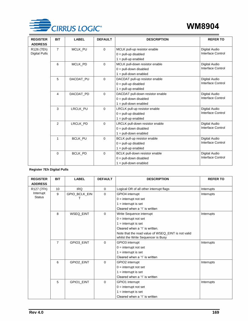
WM8904
Rev 4.0 169
REGISTER
ADDRESS
BIT LABEL DEFAULT DESCRIPTION REFER TO
R126 (7Eh)
Digital Pulls
7 MCLK_PU 0 MCLK pull-up resistor enable
0 = pull-up disabled
1 = pull-up enabled
Digital Audio
Interface Control
6 MCLK_PD 0 MCLK pull-down resistor enable
0 = pull-down disabled
1 = pull-down enabled
Digital Audio
Interface Control
5 DACDAT_PU 0 DACDAT pull-up resistor enable
0 = pull-up disabled
1 = pull-up enabled
Digital Audio
Interface Control
4 DACDAT_PD 0 DACDAT pull-down resistor enable
0 = pull-down disabled
1 = pull-down enabled
Digital Audio
Interface Control
3 LRCLK_PU 0 LRCLK pull-up resistor enable
0 = pull-up disabled
1 = pull-up enabled
Digital Audio
Interface Control
2 LRCLK_PD 0 LRCLK pull-down resistor enable
0 = pull-down disabled
1 = pull-down enabled
Digital Audio
Interface Control
1 BCLK_PU 0 BCLK pull-up resistor enable
0 = pull-up disabled
1 = pull-up enabled
Digital Audio
Interface Control
0 BCLK_PD 0 BCLK pull-down resistor enable
0 = pull-down disabled
1 = pull-down enabled
Digital Audio
Interface Control
Register 7Eh Digital Pulls
REGISTER
ADDRESS
BIT LABEL DEFAULT DESCRIPTION REFER TO
R127 (7Fh)
Interrupt
Status
10 IRQ 0 Logical OR of all other interrupt flags Interrupts
9 GPIO_BCLK_EIN
T
0 GPIO4 interrupt
0 = interrupt not set
1 = interrupt is set
Cleared when a ‘1’ is written
Interrupts
8 WSEQ_EINT 0 Write Sequence interrupt
0 = interrupt not set
1 = interrupt is set
Cleared when a ‘1’ is written.
Note that the read value of WSEQ_EINT is not valid
whilst the Write Sequencer is Busy
Interrupts
7 GPIO3_EINT 0 GPIO3 interrupt
0 = interrupt not set
1 = interrupt is set
Cleared when a ‘1’ is written
Interrupts
6 GPIO2_EINT 0 GPIO2 interrupt
0 = interrupt not set
1 = interrupt is set
Cleared when a ‘1’ is written
Interrupts
5 GPIO1_EINT 0 GPIO1 interrupt
0 = interrupt not set
1 = interrupt is set
Cleared when a ‘1’ is written
Interrupts

WM8904
170 Rev 4.0
REGISTER
ADDRESS
BIT LABEL DEFAULT DESCRIPTION REFER TO
4 GPI8_EINT 0 GPI8 interrupt
0 = interrupt not set
1 = interrupt is set
Cleared when a ‘1’ is written
Interrupts
3 GPI7_EINT 0 GPI7 interrupt
0 = interrupt not set
1 = interrupt is set
Cleared when a ‘1’ is written
Interrupts
2 FLL_LOCK_EINT 0 FLL Lock interrupt
0 = interrupt not set
1 = interrupt is set
Cleared when a ‘1’ is written
Interrupts
1 MIC_SHRT_EINT 0 MICBIAS short circuit interrupt
0 = interrupt not set
1 = interrupt is set
Cleared when a ‘1’ is written
Interrupts
0 MIC_DET_EINT 0 MICBIAS current detect interrupt
0 = interrupt not set
1 = interrupt is set
Cleared when a ‘1’ is written
Interrupts
Register 7Fh Interrupt Status
REGISTER
ADDRESS
BIT LABEL DEFAULT DESCRIPTION REFER TO
R128 (80h)
Interrupt
Status Mask
9 IM_GPIO_BCLK_
EINT
1 GPIO4 interrupt mask
0 = do not mask interrupt
1 = mask interrupt
Interrupts
8 IM_WSEQ_EINT 1 Write sequencer interrupt mask
0 = do not mask interrupt
1 = mask interrupt
Interrupts
7 IM_GPIO3_EINT 1 GPIO3 interrupt mask
0 = do not mask interrupt
1 = mask interrupt
Interrupts
6 IM_GPIO2_EINT 1 GPIO2 interrupt mask
0 = do not mask interrupt
1 = mask interrupt
Interrupts
5 IM_GPIO1_EINT 1 GPIO1 interrupt mask
0 = do not mask interrupt
1 = mask interrupt
Interrupts
4 IM_GPI8_EINT 1 GPI8 interrupt mask
0 = do not mask interrupt
1 = mask interrupt
Interrupts
3 IM_GPI7_EINT 1 GPI7 interrupt mask
0 = do not mask interrupt
1 = mask interrupt
Interrupts
2 IM_FLL_LOCK_EI
NT
1 FLL Lock interrupt mask
0 = do not mask interrupt
1 = mask interrupt
Interrupts
1 IM_MIC_SHRT_E
INT
1 MICBIAS short circuit interrupt mask
0 = do not mask interrupt
1 = mask interrupt
Interrupts
0 IM_MIC_DET_EI
NT
1 MICBIAS current detect interrupt mask Interrupts

WM8904
Rev 4.0 171
REGISTER
ADDRESS
BIT LABEL DEFAULT DESCRIPTION REFER TO
0 = do not mask interrupt
1 = mask interrupt
Register 80h Interrupt Status Mask
REGISTER
ADDRESS
BIT LABEL DEFAULT DESCRIPTION REFER TO
R129 (81h)
Interrupt
Polarity
9 GPIO_BCLK_EIN
T_POL
0 GPIO4 interrupt polarity
0 = active high
1 = active low
Interrupts
8 WSEQ_EINT_PO
L
0 Write Sequencer interrupt polarity
0 = active high (interrupt is triggered when WSEQ is
busy)
1 = active low (interrupt is triggered when WSEQ is idle)
Interrupts
7 GPIO3_EINT_PO
L
0 GPIO3 interrupt polarity
0 = active high
1 = active low
Interrupts
6 GPIO2_EINT_PO
L
0 GPIO2 interrupt polarity
0 = active high
1 = active low
Interrupts
5 GPIO1_EINT_PO
L
0 GPIO1 interrupt polarity
0 = active high
1 = active low
Interrupts
4 GPI8_EINT_POL 0 GPI8 interrupt polarity
0 = active high
1 = active low
Interrupts
3 GPI7_EINT_POL 0 GPI7 interrupt polarity
0 = active high
1 = active low
Interrupts
2 FLL_LOCK_EINT
_POL
0 FLL Lock interrupt polarity
0 = active high (interrupt is triggered when FLL Lock is
reached)
1 = active low (interrupt is triggered when FLL is not
locked)
Interrupts
1 MIC_SHRT_EINT
_POL
0 MICBIAS short circuit interrupt polarity
0 = active high
1 = active low
Interrupts
0 MIC_DET_EINT_
POL
0 MICBIAS current detect interrupt polarity
0 = active high
1 = active low
Interrupts
Register 81h Interrupt Polarity

WM8904
172 Rev 4.0
REGISTER
ADDRESS
BIT LABEL DEFAULT DESCRIPTION REFER TO
R130 (82h)
Interrupt
Debounce
9 GPIO_BCLK_EIN
T_DB
0 GPIO4 interrupt debounce
0 = disabled
1 = enabled
Interrupts
8 WSEQ_EINT_DB 0 Write Sequencer interrupt debounce enable
0 = disabled
1 = enabled
Interrupts
7 GPIO3_EINT_DB 0 GPIO3 input debounce
0 = disabled
1 = enabled
Interrupts
6 GPIO2_EINT_DB 0 GPIO2 input debounce
0 = disabled
1 = enabled
Interrupts
5 GPIO1_EINT_DB 0 GPIO1 input debounce
0 = disabled
1 = enabled
Interrupts
4 GPI8_EINT_DB 0 GPI8 input debounce
0 = disabled
1 = enabled
Interrupts
3 GPI7_EINT_DB 0 GPI7 input debounce
0 = disabled
1 = enabled
Interrupts
2 FLL_LOCK_EINT
_DB
0 FLL Lock debounce
0 = disabled
1 = enabled
Interrupts
1 MIC_SHRT_EINT
_DB
0 MICBIAS short circuit interrupt debounce
0 = disabled
1 = enabled
Interrupts
0 MIC_DET_EINT_
DB
0 MICBIAS current detect interrupt debounce
0 = disabled
1 = enabled
Interrupts
Register 82h Interrupt Debounce
REGISTER
ADDRESS
BIT LABEL DEFAULT DESCRIPTION REFER TO
R134 (86h)
EQ1
0 EQ_ENA 0 EQ enable
0 = EQ disabled
1 = EQ enabled
ReTuneTM Mobile
Parametric
Equalizer (EQ)
Register 86h EQ1
REGISTER
ADDRESS
BIT LABEL DEFAULT DESCRIPTION REFER TO
R135 (87h)
EQ2
4:0 EQ_B1_GAIN
[4:0]
0_1100 Gain for EQ band 1
00000 = -12dB
00001 = -11dB
(… 1dB steps)
01100 = 0dB
(… 1dB steps)
11000 = +12dB
11001 to 11111 = reserved
ReTuneTM Mobile
Parametric
Equalizer (EQ)
Register 87h EQ2

WM8904
Rev 4.0 173
REGISTER
ADDRESS
BIT LABEL DEFAULT DESCRIPTION REFER TO
R136 (88h)
EQ3
4:0 EQ_B2_GAIN
[4:0]
0_1100 Gain for EQ band 2
00000 = -12dB
00001 = -11dB
(… 1dB steps)
01100 = 0dB
(… 1dB steps)
11000 = +12dB
11001 to 11111 = reserved
ReTuneTM Mobile
Parametric
Equalizer (EQ)
Register 88h EQ3
REGISTER
ADDRESS
BIT LABEL DEFAULT DESCRIPTION REFER TO
R137 (89h)
EQ4
4:0 EQ_B3_GAIN
[4:0]
0_1100 Gain for EQ band 3
00000 = -12dB
00001 = -11dB
(… 1dB steps)
01100 = 0dB
(… 1dB steps)
11000 = +12dB
11001 to 11111 = reserved
ReTuneTM Mobile
Parametric
Equalizer (EQ)
Register 89h EQ4
REGISTER
ADDRESS
BIT LABEL DEFAULT DESCRIPTION REFER TO
R138 (8Ah)
EQ5
4:0 EQ_B4_GAIN
[4:0]
0_1100 Gain for EQ band 4
00000 = -12dB
00001 = -11dB
(… 1dB steps)
01100 = 0dB
(… 1dB steps)
11000 = +12dB
11001 to 11111 = reserved
ReTuneTM Mobile
Parametric
Equalizer (EQ)
Register 8Ah EQ5
REGISTER
ADDRESS
BIT LABEL DEFAULT DESCRIPTION REFER TO
R139 (8Bh)
EQ6
4:0 EQ_B5_GAIN
[4:0]
0_1100 Gain for EQ band5
00000 = -12dB
00001 = -11dB
(… 1dB steps)
01100 = 0dB
(… 1dB steps)
11000 = +12dB
11001 to 11111 = reserved
ReTuneTM Mobile
Parametric
Equalizer (EQ)
Register 8Bh EQ6

WM8904
174 Rev 4.0
REGISTER
ADDRESS
BIT LABEL DEFAULT DESCRIPTION REFER TO
R140 (8Ch)
EQ7
15:0 EQ_B1_A [15:0] 0000_1111_11
00_1010
EQ Band 1 Coefficient A ReTuneTM Mobile
Parametric
Equalizer (EQ)
Register 8Ch EQ7
REGISTER
ADDRESS
BIT LABEL DEFAULT DESCRIPTION REFER TO
R141 (8Dh)
EQ8
15:0 EQ_B1_B [15:0] 0000_0100_
0000_0000
EQ Band 1 Coefficient B ReTuneTM Mobile
Parametric
Equalizer (EQ)
Register 8Dh EQ8
REGISTER
ADDRESS
BIT LABEL DEFAULT DESCRIPTION REFER TO
R142 (8Eh)
EQ9
15:0 EQ_B1_PG [15:0] 0000_0000_11
01_1000
EQ Band 1 Coefficient PG ReTuneTM Mobile
Parametric
Equalizer (EQ)
Register 8Eh EQ9
REGISTER
ADDRESS
BIT LABEL DEFAULT DESCRIPTION REFER TO
R143 (8Fh)
EQ10
15:0 EQ_B2_A [15:0] 0001_1110_10
11_0101
EQ Band 2 Coefficient A ReTuneTM Mobile
Parametric
Equalizer (EQ)
Register 8Fh EQ10
REGISTER
ADDRESS
BIT LABEL DEFAULT DESCRIPTION REFER TO
R144 (90h)
EQ11
15:0 EQ_B2_B [15:0] 1111_0001_01
00_0101
EQ Band 2 Coefficient B ReTuneTM Mobile
Parametric
Equalizer (EQ)
Register 90h EQ11
REGISTER
ADDRESS
BIT LABEL DEFAULT DESCRIPTION REFER TO
R145 (91h)
EQ12
15:0 EQ_B2_C [15:0] 0000_1011_01
11_0101
EQ Band 2 Coefficient C ReTuneTM Mobile
Parametric
Equalizer (EQ)
Register 91h EQ12
REGISTER
ADDRESS
BIT LABEL DEFAULT DESCRIPTION REFER TO
R146 (92h)
EQ13
15:0 EQ_B2_PG [15:0] 0000_0001_11
00_0101
EQ Band 2 Coefficient PG ReTuneTM Mobile
Parametric
Equalizer (EQ)
Register 92h EQ13
REGISTER
ADDRESS
BIT LABEL DEFAULT DESCRIPTION REFER TO
R147 (93h)
EQ14
15:0 EQ_B3_A [15:0] 0001_1100_01
01_1000
EQ Band 3 Coefficient A ReTuneTM Mobile
Parametric
Equalizer (EQ)
Register 93h EQ14

WM8904
Rev 4.0 175
REGISTER
ADDRESS
BIT LABEL DEFAULT DESCRIPTION REFER TO
R148 (94h)
EQ15
15:0 EQ_B3_B [15:0] 1111_0011_01
11_0011
EQ Band 3 Coefficient B ReTuneTM Mobile
Parametric
Equalizer (EQ)
Register 94h EQ15
REGISTER
ADDRESS
BIT LABEL DEFAULT DESCRIPTION REFER TO
R149 (95h)
EQ16
15:0 EQ_B3_C [15:0] 0000_1010_01
01_0100
EQ Band 3 Coefficient C ReTuneTM Mobile
Parametric
Equalizer (EQ)
Register 95h EQ16
REGISTER
ADDRESS
BIT LABEL DEFAULT DESCRIPTION REFER TO
R150 (96h)
EQ17
15:0 EQ_B3_PG [15:0] 0000_0101_01
01_1000
EQ Band 3 Coefficient PG ReTuneTM Mobile
Parametric
Equalizer (EQ)
Register 96h EQ17
REGISTER
ADDRESS
BIT LABEL DEFAULT DESCRIPTION REFER TO
R151 (97h)
EQ18
15:0 EQ_B4_A [15:0] 0001_0110_10
00_1110
EQ Band 4 Coefficient A ReTuneTM Mobile
Parametric
Equalizer (EQ)
Register 97h EQ18
REGISTER
ADDRESS
BIT LABEL DEFAULT DESCRIPTION REFER TO
R152 (98h)
EQ19
15:0 EQ_B4_B [15:0] 1111_1000_00
10_1001
EQ Band 4 Coefficient B ReTuneTM Mobile
Parametric
Equalizer (EQ)
Register 98h EQ19
REGISTER
ADDRESS
BIT LABEL DEFAULT DESCRIPTION REFER TO
R153 (99h)
EQ20
15:0 EQ_B4_C [15:0] 0000_0111_10
10_1101
EQ Band 4 Coefficient C ReTuneTM Mobile
Parametric
Equalizer (EQ)
Register 99h EQ20
REGISTER
ADDRESS
BIT LABEL DEFAULT DESCRIPTION REFER TO
R154 (9Ah)
EQ21
15:0 EQ_B4_PG [15:0] 0001_0001_00
00_0011
EQ Band 4 Coefficient PG ReTuneTM Mobile
Parametric
Equalizer (EQ)
Register 9Ah EQ21
REGISTER
ADDRESS
BIT LABEL DEFAULT DESCRIPTION REFER TO
R155 (9Bh)
EQ22
15:0 EQ_B5_A [15:0] 0000_0101_01
10_0100
EQ Band 5 Coefficient A ReTuneTM Mobile
Parametric
Equalizer (EQ)
Register 9Bh EQ22

WM8904
176 Rev 4.0
REGISTER
ADDRESS
BIT LABEL DEFAULT DESCRIPTION REFER TO
R156 (9Ch)
EQ23
15:0 EQ_B5_B [15:0] 0000_0101_01
01_1001
EQ Band 1 Coefficient B ReTuneTM Mobile
Parametric
Equalizer (EQ)
Register 9Ch EQ23
REGISTER
ADDRESS
BIT LABEL DEFAULT DESCRIPTION REFER TO
R157 (9Dh)
EQ24
15:0 EQ_B5_PG [15:0] 0100_0000_00
00_0000
EQ Band 5 Coefficient PG ReTuneTM Mobile
Parametric
Equalizer (EQ)
Register 9Dh EQ24
REGISTER
ADDRESS
BIT LABEL DEFAULT DESCRIPTION REFER TO
R198 (C6h)
ADC Test 0
2 ADC_128_OSR
_TST_MODE
0 ADC Bias Control (1)
Set this bit to 1 in ADC 64fs mode (ADC_OSR128 = 0).
Set this bit to 0 in ADC 128fs mode (ADC_OSR128 = 1).
ADC
Oversampling
Ratio (OSR)
0 ADC_BIASX1P5 0 ADC Bias Control (2)
Set this bit to 1 in ADC 64fs mode (ADC_OSR128 = 0).
Set this bit to 0 in ADC 128fs mode (ADC_OSR128 = 1).
ADC
Oversampling
Ratio (OSR)
Register C6h ADC Test 0
REGISTER
ADDRESS
BIT LABEL DEFAULT DESCRIPTION REFER TO
R247 (F7h)
FLL NCO
Test 0
0 FLL_FRC_NCO 0 FLL Forced control select
0 = Normal
1 = FLL oscillator controlled by FLL_FRC_NCO_VAL
(Note that this field is required for free-running FLL modes
only)
Frequency Locked
Loop (FLL)
Register F7h FLL NCO Test 0
REGISTER
ADDRESS
BIT LABEL DEFAULT DESCRIPTION REFER TO
R248 (F8h)
FLL NCO
Test 1
5:0 FLL_FRC_NCO
_VAL [5:0]
01_1001 FLL Forced oscillator value
Valid range is 000000 to 111111
0x19h (011001) = 12MHz approx
(Note that this field is required for free-running FLL modes
only)
Frequency Locked
Loop (FLL)
Register F8h FLL NCO Test 1

WM8904
Rev 4.0 177
APPLICATIONS INFORMATION
RECOMMENDED EXTERNAL COMPONENTS
Figure 71 Recommended External Components
Notes:
1. Decoupling Capacitors
X5R ceramic capacitor is recommended for capacitors C1, C2, C3, C4, C5, C15, C16, C17 and C18.
The positioning of C17 and C18 is very important - these should be as close to the WM8904 as possible.
Capacitors C15 and C16 should also be positioned as close to the WM8904 as possible.
2. Charge Pump Capacitors
Specific recommendations for C14, C15 and C16 are provided in Table 95. Note that two different recommendations are
provided for C15 and C16; either of these components is suitable, depending upon size requirements and availability.
The positioning of C14 is very important - this should be as close to the WM8904 as possible.
It is important to select a suitable capacitor type for the Charge Pump. Note that the capacitance may vary with DC voltage;
care is required to ensure that required capacitance is achieved at the applicable operating voltage, as specified in Table 95.
The capacitor datasheet should be consulted for this information.
COMPONENT REQUIRED
CAPACITANCE
VALUE PART NUMBER VOLTAGE TYPE SIZE
C14 (CPCA-CPCB) 1F at 2VDC 2.2F Kemet C0402C225M9PAC 6.3v X5R 0402
C15 (CPVOUTN)
C16 (CPVOUTP) 2F at 2VDC
2.2F MuRata GRM188R61A225KE34D 10v X5R 0603
4.7F MuRata GRM155R60J475M_EIA 6.3v X5R 0402
Table 95 Charge Pump Capacitors

WM8904
178 Rev 4.0
3. Zobel Networks
The Zobel network shown in Figure 71 is required on HPOUTL, HPOUTR, LINEOUTL and LINEOUTR whenever that output is
enabled. Stability of these ground-referenced outputs across all process corners cannot be guaranteed without the Zobel
network components. (Note that, if any ground-referenced output pin is not required, the zobel network components can be
omitted from the output pin, and the pin can be left floating.) The Zobel network requirement is detailed further in the
applications note WAN_0212 “Class W Headphone Impedance Compensation”.
Zobel networks (C6, C7, C8, C9, R1, R2, R3, R4) should be positioned reasonably close to the WM8904.
4. Microphone Grounding
R7 and R8 can be populated with other values to remove common mode noise on the microphone if required.

WM8904
Rev 4.0 179
MIC DETECTION SEQUENCE USING MICBIAS CURRENT
This section details an example sequence which summarises how the host processor can configure
and detect the events supported by the MICBIAS current detect function (see “Electret Condenser
Microphone Interface”):
Mic insertion/removal
Hook switch press/release
Figure 72 shows an example of how the MICBIAS current flow varies versus time, during mic insertion
and hook switch events. The Y axis is annotated with the Mic detection thresholds, and the X axis is
annotated with the stages of an example sequence as detailed in Table 96, to illustrate how the host
processor can implement mic insertion and hook switch detection.
The sequence assumes that the microphone insertion and hook switch detection functions are
monitored by polling the interrupt flags using the control interface. Note that the maximum mechanical
bounce times for mic insertion and removal must be fully understood by the software programmer.
A GPIO pin could be used as an alternative mechanism to monitor the MICBIAS detection functions.
This enables the host processor to detect mechanical bounce at any time.
Time
Mic Hook Switch Threshold
Mic Detect Interrupt
MIC
BIA
S C
urr
en
t
(1) (2) (4) (5) (6) (7) (8) (9)
TDETTDET
Mic Detect Threshold
Hysteresis
(3) (10)
TSHORT
TSHORT
Mic Detect Interrupt Polarity
Mic Short Interrupt
Mic Short Interrupt Polarity
MIC_DET_EINT
MIC_DET_EINT_POL
MIC_SHRT_EINT
MIC_SHRT_EINT_POL
HOST
PROCESSOR
Read the Mic detect interrupt
flag. If high, can then set
MIC_DET_EINT_POL to 1,
but only if mechanical bounce
phase has finished. Clear
MIC_DET_EINT by writing ‘1’.
Read the Hook switch interrupt flag.
If high, can immediately set
MIC_SHRT_EINT_POL to 1. Clear
MIC_SHRT_EINT by writing ‘1’.
Read the Hook switch interrupt flag. If high, can
immediately clear MIC_SHRT_EINT_POL to 0.
Clear MIC_SHRT_EINT by writing ‘1’.
Read the Mic detect interrupt flag. If high, can
then clear MIC_DET_EINT_POL to 0, but only
if mechanical bounce phase has finished.
Clear MIC_DET_EINT by writing ‘1’.
Step
(1) (2) (4) (5) (6) (7) (8) (9)(3) (10)Step
Example plot of MICBIAS Current versus time
Mic inserted
Hook switch
pressed
Figure 72 Mic Insert and Hook Switch Detect: Example MICBIAS Current Plot

WM8904
180 Rev 4.0
STEP DETAILS
1 Mic not inserted. To detect mic insertion, Host processor must initialise interrupts and clear MIC_DET_EINT_POL = 0.
At every step, the host processor should poll the interrupt status register.
Note that Mic Insertion de-bounce circuitry can be enabled by setting MIC_DET_EINT_DB = 1.
2 Mechanical bounce of jack socket during Mic insertion. Host processor may already detect a mic insertion interrupt
(MIC_DET_EINT) during this step. Once detected, the host processor can set MIC_DET_EINT_POL = 1 and then
clear the interrupt, unless mechanical bounce can last longer than the shortest possible TDET, in which case the host
processor should wait until step 3.
3 Mic fully inserted. If not already set, the host processor must now set MIC_DET_EINT_POL = 1. If not already cleared,
the host processor must now clear the MIC_DET_EINT interrupt. To detect Hook switch press, the host processor
must clear MIC_SHRT_EINT_POL = 0. At this step, the diagram shows no AC current swing, due to a very low
ambient noise level.
4 Mic fully inserted. Diagram shows AC current swing due to high levels of background noise (such as wind).
5 Mechanical bounce during hook switch press. The hook switch interrupt is unlikely to be set during this step, because
10 successive samples of the MICBIAS current exceeding the hook switch threshold have not yet been sampled.
Note that Hook Switch de-bounce circuitry can be enabled by setting MIC_SHRT_EINT_DB = 1.
6 Hook switch is fully pressed down. After TSHORT, 10 successive samples of the MICBIAS current exceeding the hook
switch threshold have been detected, hence a hook switch interrupt (MIC_SHRT_EINT) will be generated. Once
detected, the host processor can immediately set MIC_SHRT_EINT_POL = 1 and then clear the MIC_SHRT_EINT
interrupt.
7 Mechanical bounce during hook switch release. The hook switch interrupt is unlikely to be set during this step, because
10 successive samples of the MICBIAS current lower than the hook switch threshold have not yet been sampled.
8 Hook switch fully released. After TSHORT, 10 successive samples of the MICBIAS current lower than the hook switch
threshold have been detected, hence a hook switch interrupt (MIC_SHRT_EINT) will be generated. Once detected, the
host processor can immediately clear MIC_SHRT_EINT_POL = 0 and then clear the MIC_SHRT_EINT interrupt.
9 Mechanical bounce of jack socket during Mic removal. Host processor may already detect a mic removal interrupt
(MIC_DET_EINT) during this step. Once detected, the host processor can clear MIC_DET_EINT_POL = 0 and then
clear the interrupt, unless mechanical bounce can last longer than the shortest possible TDET, in which case the host
processor should wait until step 10.
10 Mic fully removed. If not already cleared, the host processor must now clear MIC_DET_EINT_POL = 0. If not already
cleared, the host processor must now clear the MIC_DET_EINT interrupt.
Table 96 Mic Insert and Hook Switch Detect: Example Sequence
Alternatively, utilising a GPIO pin to monitor the MICBIAS current detect functionality permits the host
processor to monitor the steady state of microphone detection or hook switch press functions.
Because the GPIO shows the steady state condition, software de-bounce may be easier to implement
in the host processor, dependant on the processor performance characteristics, hence use of the
GPIO is likely to simplify the rejection of mechanical bounce. Changes of state in the GPIO pin are
also subject to the time delays tDET and tSHORT.

WM8904
Rev 4.0 181
PACKAGE DIMENSIONS
The 36-ball W-CSP package drawing is shown below.
B: 36 BALL W-CSP PACKAGE 2.651 X 2.525 X 0.504mm BODY, 0.40 mm BALL PITCH
A1
CORNER
TOP VIEW
E
Aaaa2 X
D
5
4
DETAIL 2
DETAIL 2
A
A2
2
Baaa2 X
A1
Zbbb
Z
1
E1
A
D1
DETAIL 1
D
C
B
F
E
e
e
BOTTOM VIEW
16 5 4 3 2
g
NOTES:
1. PRIMARY DATUM -Z- AND SEATING PLANE ARE DEFINED BY THE SPHERICAL CROWNS OF THE SOLDER BALLS.
2. THIS DIMENSION INCLUDES STAND-OFF HEIGHT ‘A1’ AND BACKSIDE COATING.
3. A1 CORNER IS IDENTIFIED BY INK/LASER MARK ON TOP PACKAGE.
4. BILATERAL TOLERANCE ZONE IS APPLIED TO EACH SIDE OF THE PACKAGE BODY.
5. ‘e’ REPRESENTS THE BASIC SOLDER BALL GRID PITCH.
6. THIS DRAWING IS SUBJECT TO CHANGE WITHOUT NOTICE.
7. FOLLOWS JEDEC DESIGN GUIDE MO-211-C.
A1 0.172
D
D1
E
E1
e
2.000 BSC
2.525
0.326 BSC
2.000 BSC
0.400 BSC
2.651
Dimensions (mm)Symbols
MIN NOM MAX NOTE
A 0.504
A2 0.265 0.280 0.295
5
f1
0.5380.470
0.202 0.232
g 0.022
h 0.262
f2 0.263 BSC
f1
f2
h
DM066.D
2.621 2.681
2.495 2.555
0.222 0.302
4
A
BZddd M A B
Zccc
aaa
bbb
ccc
ddd
0.025
0.060
0.030
0.015
DETAIL 1
0.0250.019
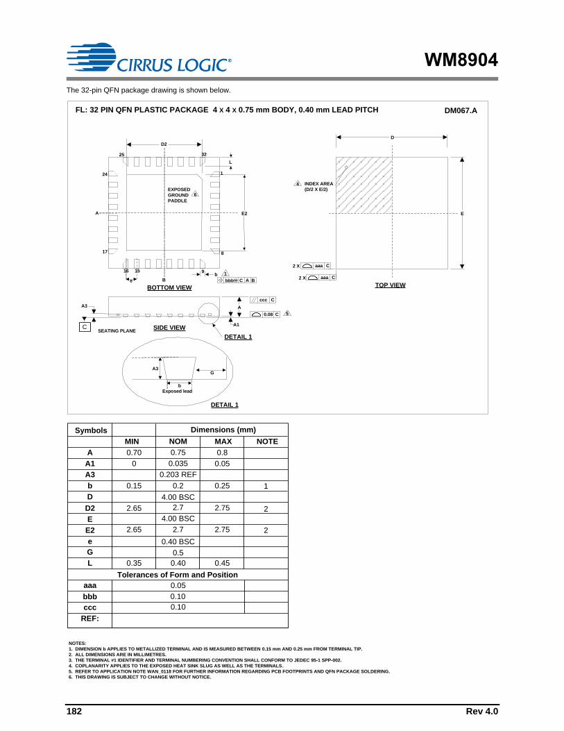
WM8904
182 Rev 4.0
The 32-pin QFN package drawing is shown below.
FL: 32 PIN QFN PLASTIC PACKAGE 4 X 4 X 0.75 mm BODY, 0.40 mm LEAD PITCH
E2
bB
15
A
8
9
e
C0.08
Cccc
A
A1C
A3
SEATING PLANE
1
L
INDEX AREA
(D/2 X E/2)
TOP VIEW
D
Caaa2 X
Caaa2 X
E
1
17
24
25 32
D2
BCbbb M A
5
4
NOTES:
1. DIMENSION b APPLIES TO METALLIZED TERMINAL AND IS MEASURED BETWEEN 0.15 mm AND 0.25 mm FROM TERMINAL TIP.
2. ALL DIMENSIONS ARE IN MILLIMETRES.
3. THE TERMINAL #1 IDENTIFIER AND TERMINAL NUMBERING CONVENTION SHALL CONFORM TO JEDEC 95-1 SPP-002.
4. COPLANARITY APPLIES TO THE EXPOSED HEAT SINK SLUG AS WELL AS THE TERMINALS.
5. REFER TO APPLICATION NOTE WAN_0118 FOR FURTHER INFORMATION REGARDING PCB FOOTPRINTS AND QFN PACKAGE SOLDERING.
6. THIS DRAWING IS SUBJECT TO CHANGE WITHOUT NOTICE.
A3G
b
Exposed lead
DETAIL 1
DETAIL 1
EXPOSED
GROUND
PADDLE
6
BOTTOM VIEW
SIDE VIEW
16
DM067.A
Dimensions (mm)Symbols
MIN NOM MAX NOTE
A
A1
A3
0.70 0.75 0.8
0.050.0350
0.203 REF
b
D
D2
E
E2
e
L
0.250.15
4.00 BSC
2.752.72.65
0.40 BSC
0.35 0.40 0.45
1
2
2
4.00 BSC
2.752.72.65
0.10
aaa
bbb
ccc
REF:
0.05
0.10
Tolerances of Form and Position
0.2
0.5G

WM8904
Rev 4.0 183
IMPORTANT NOTICE
Contacting Cirrus Logic Support For all product questions and inquiries, contact a Cirrus Logic Sales Representative.
To find one nearest you, go to www.cirrus.com.
"Pre-Production” product information describes products that are in production, but for which full characterization data is not yet
available. For the purposes of our terms and conditions of sale, "Preliminary" or "Advanced" datasheets are non-final datasheets
that include but are not limited to datasheets marked as “Target”, “Advance”, “Product Preview”, “Preliminary Technical Data”
and/or “Pre-production.” Products provided with any such datasheet are therefore subject to relevant terms and conditions
associated with "Preliminary" or "Advanced" designations. The products and services of Cirrus Logic International (UK) Limited;
Cirrus Logic, Inc.; and other companies in the Cirrus Logic group (collectively either “Cirrus Logic” or “Cirrus”) are sold subject to
Cirrus Logic’s terms and conditions of sale supplied at the time of order acknowledgment, including those pertaining to warranty,
indemnification, and limitation of liability. Software is provided pursuant to applicable license terms. Cirrus Logic reserves the right
to make changes to its products and specifications or to discontinue any product or service without notice. Customers should
therefore obtain the latest version of relevant information from Cirrus Logic to verify that the information is current and complete.
Testing and other quality control techniques are utilized to the extent Cirrus Logic deems necessary. Specific testing of all
parameters of each device is not necessarily performed. In order to minimize risks associated with customer applications, the
customer must use adequate design and operating safeguards to minimize inherent or procedural hazards. Cirrus Logic is not
liable for applications assistance or customer product design. The customer is solely responsible for its selection and use of Cirrus
Logic products. Use of Cirrus Logic products may entail a choice between many different modes of operation, some or all of which
may require action by the user, and some or all of which may be optional. Nothing in these materials should be interpreted as
instructions or suggestions to choose one mode over another. Likewise, description of a single mode should not be interpreted as a
suggestion that other modes should not be used or that they would not be suitable for operation. Features and operations
described herein are for illustrative purposes only.
CERTAIN APPLICATIONS USING SEMICONDUCTOR PRODUCTS MAY INVOLVE POTENTIAL RISKS OF DEATH, PERSONAL
INJURY, OR SEVERE PROPERTY OR ENVIRONMENTAL DAMAGE (“CRITICAL APPLICATIONS”). CIRRUS LOGIC
PRODUCTS ARE NOT DESIGNED, AUTHORIZED OR WARRANTED FOR USE IN PRODUCTS SURGICALLY IMPLANTED
INTO THE BODY, AUTOMOTIVE SAFETY OR SECURITY DEVICES, NUCLEAR SYSTEMS, LIFE SUPPORT PRODUCTS OR
OTHER CRITICAL APPLICATIONS. INCLUSION OF CIRRUS LOGIC PRODUCTS IN SUCH APPLICATIONS IS UNDERSTOOD
TO BE FULLY AT THE CUSTOMER’S RISK AND CIRRUS LOGIC DISCLAIMS AND MAKES NO WARRANTY, EXPRESS,
STATUTORY OR IMPLIED, INCLUDING THE IMPLIED WARRANTIES OF MERCHANTABILITY AND FITNESS FOR
PARTICULAR PURPOSE, WITH REGARD TO ANY CIRRUS LOGIC PRODUCT THAT IS USED IN SUCH A MANNER. IF THE
CUSTOMER OR CUSTOMER’S CUSTOMER USES OR PERMITS THE USE OF CIRRUS LOGIC PRODUCTS IN CRITICAL
APPLICATIONS, CUSTOMER AGREES, BY SUCH USE, TO FULLY INDEMNIFY CIRRUS LOGIC, ITS OFFICERS, DIRECTORS,
EMPLOYEES, DISTRIBUTORS AND OTHER AGENTS FROM ANY AND ALL LIABILITY, INCLUDING ATTORNEYS’ FEES AND
COSTS, THAT MAY RESULT FROM OR ARISE IN CONNECTION WITH THESE USES.
This document is the property of Cirrus Logic and by furnishing this information, Cirrus Logic grants no license, express or implied,
under any patents, mask work rights, copyrights, trademarks, trade secrets or other intellectual property rights. Any provision or
publication of any third party’s products or services does not constitute Cirrus Logic’s approval, license, warranty or endorsement
thereof. Cirrus Logic gives consent for copies to be made of the information contained herein only for use within your organization
with respect to Cirrus Logic integrated circuits or other products of Cirrus Logic, and only if the reproduction is without alteration
and is accompanied by all associated copyright, proprietary and other notices and conditions (including this notice). This consent
does not extend to other copying such as copying for general distribution, advertising or promotional purposes, or for creating any
work for resale. This document and its information is provided “AS IS” without warranty of any kind (express or implied). All
statutory warranties and conditions are excluded to the fullest extent possible. No responsibility is assumed by Cirrus Logic for the
use of information herein, including use of this information as the basis for manufacture or sale of any items, or for infringement of
patents or other rights of third parties. Cirrus Logic, Cirrus, the Cirrus Logic logo design, SoundClear, WISCE, SmartDAC, and
SilentSwitch are among the trademarks of Cirrus Logic. Other brand and product names may be trademarks or service marks of
their respective owners.
Copyright © 2009–2016 Cirrus Logic, Inc. All rights reserved.

WM8904
184 Rev 4.0
REVISION HISTORY
DATE REV DESCRIPTION OF CHANGES PAGE CHANGED BY
05/08/11 3.3 Low Power Playback mode definition and characteristics added.
ISEL (bias control) register added
22,23,81,
82,142
PH
10/01/12 3.3 Order codes updated to WM8904CGEFL/V and WM8904CGEFL/RV
to reflect change to copper wire bonding
8 JMacD
24/08/12 3.3 36 Ball package diagram updated to DM066.C 185 JMacD
27/08/12 3.3 Headline DAC to headphone playback power consumption updated
to 3.0mW.
1 ssaunders
03/09/12 3.3 W-CSP reel quantity changed to 5,000 8 JMacD
24/06/14 3.4 W-CSP reel quantity changed to 3,500 8 JMacD
11/11/16 3.5 36-ball package drawing updated to DM066.D 181 PH
21/12/16 4.0 Revision status updated PH