Embed Size (px)
Citation preview
Work in Progress --- Not for Publication1 ERD WG 7/10/11 San Francisco FxF Meeting
2011 ERD Critical Review Survey
2011 Process for Critically Reviewing Emerging Research Logic
and Memory Devices
Work in Progress --- Not for Publication2 ERD WG 7/10/11 San Francisco FxF Meeting
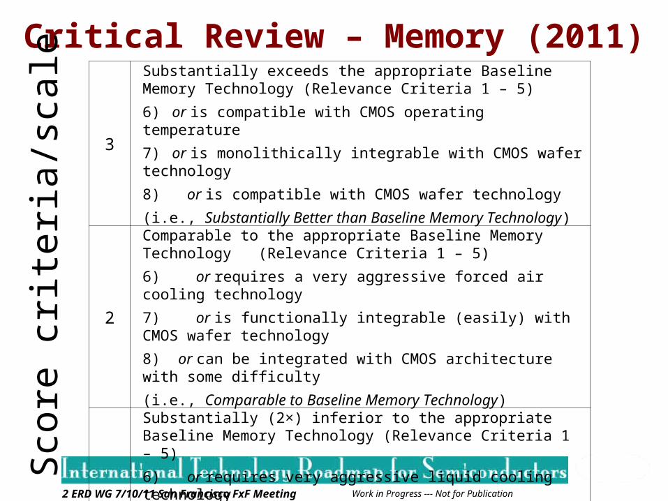
Critical Review – Memory (2011)S
core
cri
teri
a/sc
ale 3
Substantially exceeds the appropriate Baseline Memory Technology (Relevance Criteria 1 – 5)
6) or is compatible with CMOS operating temperature
7) or is monolithically integrable with CMOS wafer technology
8) or is compatible with CMOS wafer technology
(i.e., Substantially Better than Baseline Memory Technology)
2
Comparable to the appropriate Baseline Memory Technology (Relevance Criteria 1 – 5)
6) or requires a very aggressive forced air cooling technology
7) or is functionally integrable (easily) with CMOS wafer technology
8) or can be integrated with CMOS architecture with some difficulty
(i.e., Comparable to Baseline Memory Technology)
1
Substantially (2×) inferior to the appropriate Baseline Memory Technology (Relevance Criteria 1 – 5)
6) or requires very aggressive liquid cooling technology
7) or is not integrable with CMOS wafer technology
8) or can not be integrated with CMOS architecture
(i.e., Substantially Worse than Baseline Memory Technology)
Work in Progress --- Not for Publication3 ERD WG 7/10/11 San Francisco FxF Meeting
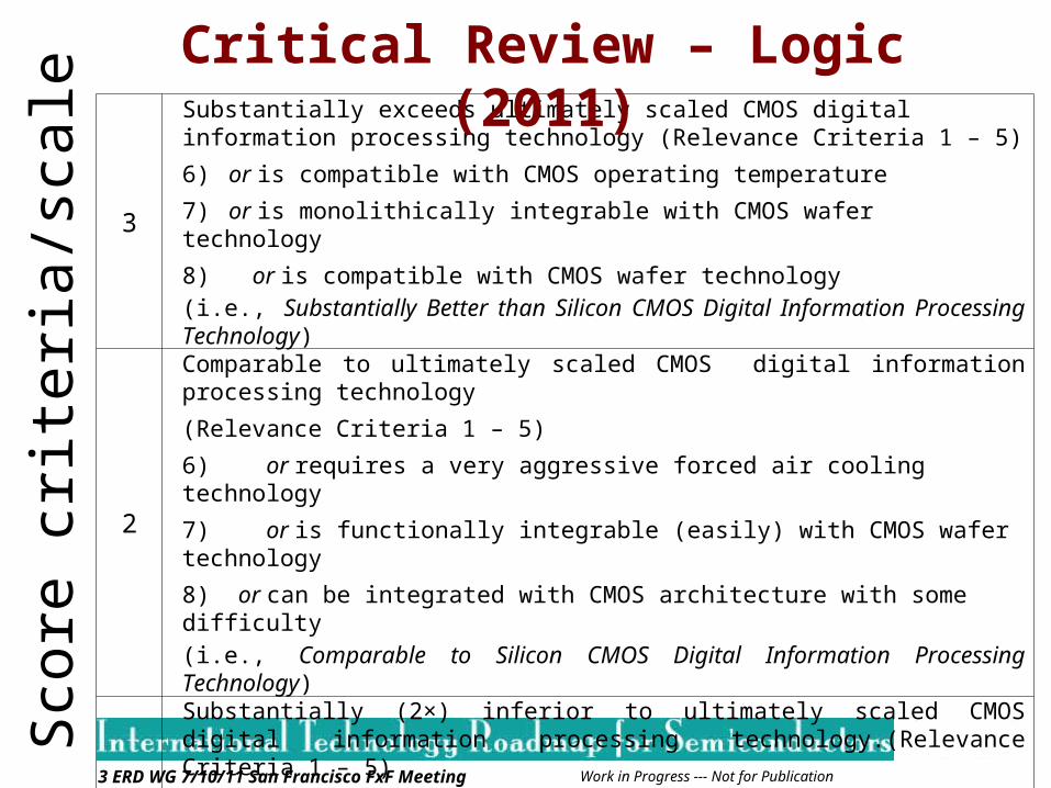
3
Substantially exceeds ultimately scaled CMOS digital information processing technology (Relevance Criteria 1 – 5)
6) or is compatible with CMOS operating temperature
7) or is monolithically integrable with CMOS wafer technology
8) or is compatible with CMOS wafer technology
(i.e., Substantially Better than Silicon CMOS Digital Information Processing Technology)
2
Comparable to ultimately scaled CMOS digital information processing technology
(Relevance Criteria 1 – 5)
6) or requires a very aggressive forced air cooling technology
7) or is functionally integrable (easily) with CMOS wafer technology
8) or can be integrated with CMOS architecture with some difficulty
(i.e., Comparable to Silicon CMOS Digital Information Processing Technology)
1
Substantially (2×) inferior to ultimately scaled CMOS digital information processing technology.(Relevance Criteria 1 – 5)
6) or requires very aggressive liquid cooling technology
7) or is not integrable with CMOS wafer technology
8) or can not be integrated with CMOS architecture
(i.e., Substantially Worse than Silicon CMOS Digital Information Processing Technology)
Critical Review – Logic (2011)S
core
cri
teri
a/sc
ale
Work in Progress --- Not for Publication4 ERD WG 7/10/11 San Francisco FxF Meeting
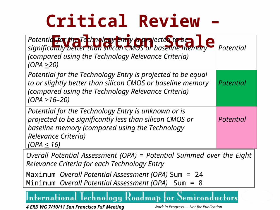
Critical Review – Evaluation Scale
Overall Potential Assessment (OPA) = Potential Summed over the Eight Relevance Criteria for each Technology Entry
Maximum Overall Potential Assessment (OPA) Sum = 24Minimum Overall Potential Assessment (OPA) Sum = 8
Potential for the Technology Entry is projected to be significantly better than silicon CMOS or baseline memory (compared using the Technology Relevance Criteria) (OPA >20)
Potential
Potential for the Technology Entry is projected to be equal to or slightly better than silicon CMOS or baseline memory (compared using the Technology Relevance Criteria)(OPA >16–20)
Potential
Potential for the Technology Entry is unknown or is projected to be significantly less than silicon CMOS or baseline memory (compared using the Technology Relevance Criteria)(OPA < 16)
Potential
Work in Progress --- Not for Publication5 ERD WG 7/10/11 San Francisco FxF Meeting
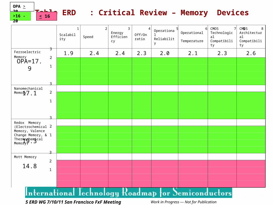
Scalability SpeedEnergy Efficiency
Off/On ratio
Operational Reliability
Operational Temperature
CMOS Technological Compatibility
CMOS Architectural Compatibility
Ferroelectric Memory
1.9 2.4 2.4 2.3 2.0 2.1 2.3 2.6
Nanomechanical Memory
Redox Memory (Electrochemical Memory, Valence Change Memory, & Thermochemical Memory)
Mott Memory
3
2
1
3
2
1
3
2
1
3
2
1
Table ERD : Critical Review – Memory DevicesOPA > 20
>16 - 20 < 16
81 3 12 5 14 7 16
OPA=17.9
17.1
19.3
14.8
Work in Progress --- Not for Publication6 ERD WG 7/10/11 San Francisco FxF Meeting
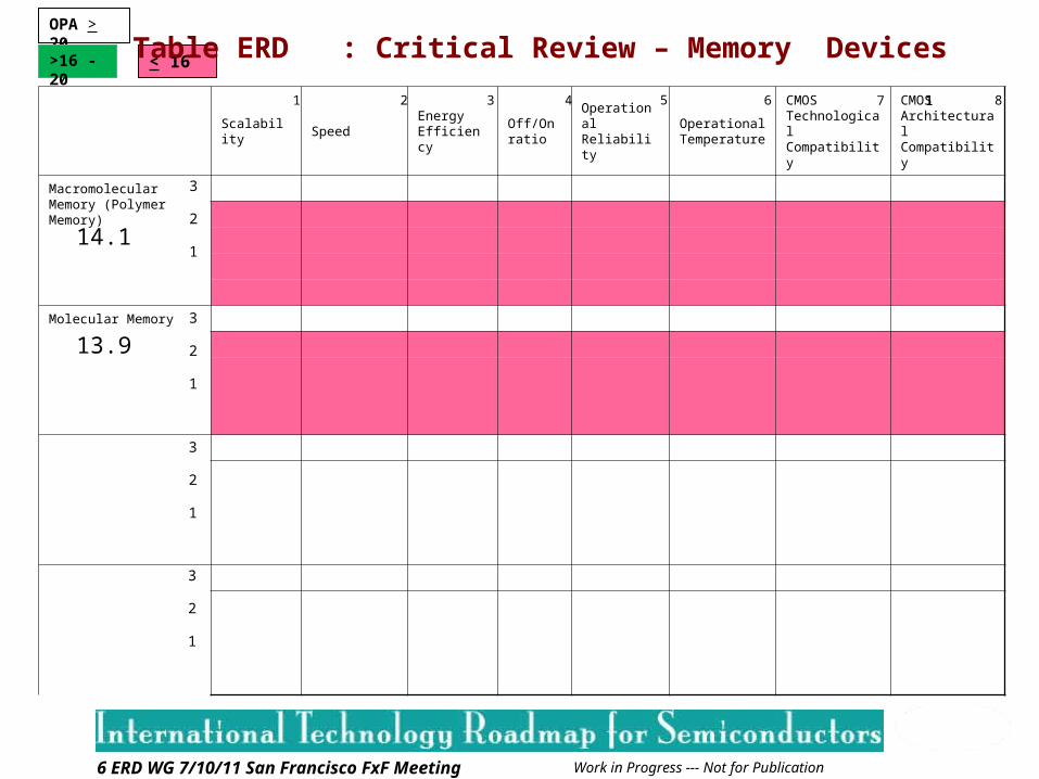
Scalability SpeedEnergy Efficiency
Off/On ratio
Operational Reliability
Operational Temperature
CMOS Technological Compatibility
CMOS Architectural Compatibility
Macromolecular Memory (Polymer Memory)
Molecular Memory
3
2
1
3
2
1
3
2
1
3
2
1
OPA > 20
>16 - 20 < 16
81 3 12 5 14 76
Table ERD : Critical Review – Memory Devices
14.1
13.9
Work in Progress --- Not for Publication7 ERD WG 7/10/11 San Francisco FxF Meeting
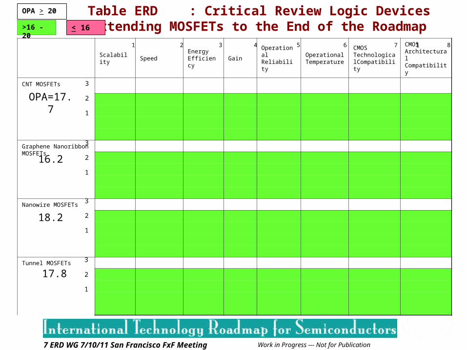
Scalability SpeedEnergy Efficiency
GainOperational Reliability
Operational Temperature
CMOS TechnologicalCompatibility
CMOS Architectural Compatibility
CNT MOSFETs
Graphene Nanoribbon MOSFETs
Nanowire MOSFETs
Tunnel MOSFETs
3
2
1
3
2
1
3
2
1
3
2
1
Table ERD : Critical Review Logic DevicesExtending MOSFETs to the End of the Roadmap
OPA > 20
>16 - 20 < 16
81 3 12 5 14 76
OPA=17.7
16.2
18.2
17.8
Work in Progress --- Not for Publication8 ERD WG 7/10/11 San Francisco FxF Meeting
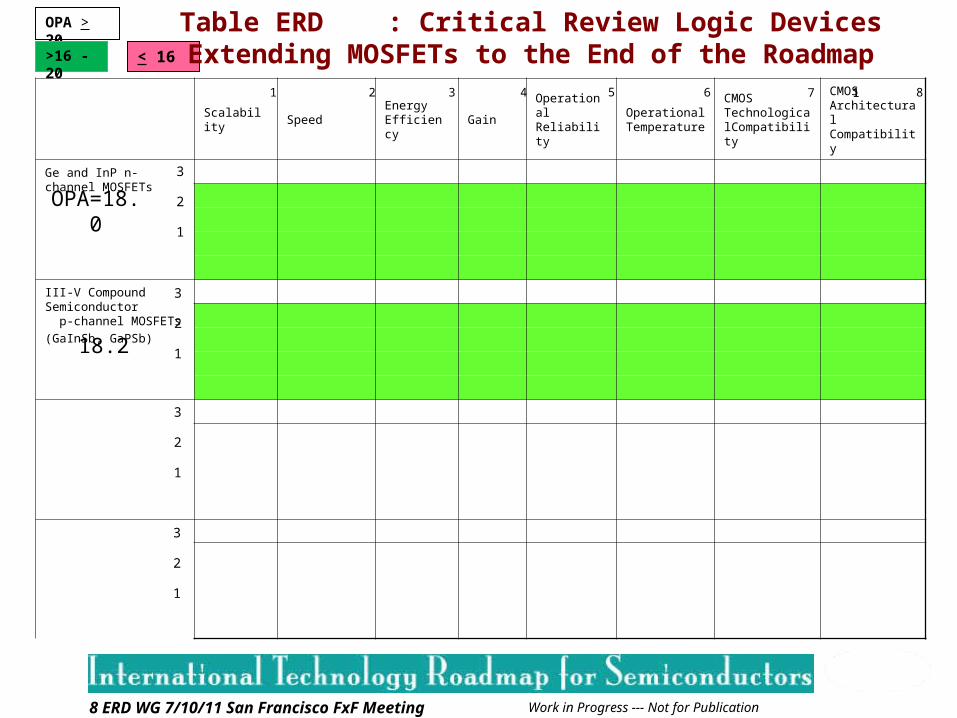
Scalability SpeedEnergy Efficiency
GainOperational Reliability
Operational Temperature
CMOS TechnologicalCompatibility
CMOS Architectural Compatibility
Ge and InP n-channel MOSFETs
III-V Compound Semiconductor p-channel MOSFETs(GaInSb, GaPSb)
3
2
1
3
2
1
3
2
1
OPA > 20
>16 - 20 < 16
81 3 12 5 14 76
3
2
1
Table ERD : Critical Review Logic DevicesExtending MOSFETs to the End of the Roadmap
OPA=18.0
18.2

Work in Progress --- Not for Publication9 ERD WG 7/10/11 San Francisco FxF Meeting
Scalability SpeedEnergy Efficiency
GainOperational Reliability
Operational Temperature
CMOS TechnologicalCompatibility
CMOS Architectural Compatibility
Spin FET and Spin MOSET
I MOSFETs
NEMs Devices
Atomic Switch
3
2
1
3
2
1
3
2
1
3
2
1
OPA > 20
>16 - 20 < 16
81 3 12 5 14 76
Table ERD : Critical Review Logic DevicesNon-conventional FETs and other Charge-based Devices
OPA=16.2
16.6
15.7
15.7
Work in Progress --- Not for Publication10 ERD WG 7/10/11 San Francisco FxF Meeting
Scalability SpeedEnergy Efficiency
GainOperational Reliability
Operational Temperature
CMOS TechnologicalCompatibility
CMOS Architectural Compatibility
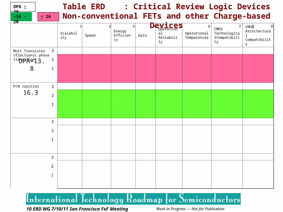
Mott Transistor (Electronic phase transition)
P/N Junction
3
2
1
3
2
1
3
2
1
3
2
1
OPA > 20
>16 - 20 < 16
81 3 12 5 14 76
Table ERD : Critical Review Logic DevicesNon-conventional FETs and other Charge-based Devices
16.3
OPA=13.8
Work in Progress --- Not for Publication11 ERD WG 7/10/11 San Francisco FxF Meeting
Scalability SpeedEnergy Efficiency
GainOperational Reliability
Operational Temperature
CMOS TechnologicalCompatibility
CMOS Architectural Compatibility
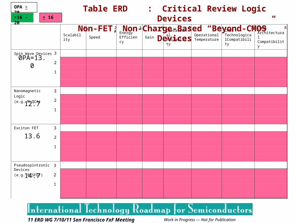
Spin Wave Devices
Nanomagnetic Logic(e.g. M:QCA)
Exciton FET
Pseudospintronic Devices (e.g. BISFET)
3
2
1
3
2
1
3
2
1
3
2
1
Table ERD : Critical Review Logic DevicesNon-FET, Non-Charge-Based “Beyond-CMOS” Devices
OPA > 20
>16 - 20 < 16
81 3 12 5 14 76
12.7
13.6
14.7
0PA=13.0

Work in Progress --- Not for Publication12 ERD WG 7/10/11 San Francisco FxF Meeting
Scalability SpeedEnergy Efficiency
GainOperational Reliability
Operational Temperature
CMOS TechnologicalCompatibility
CMOS Architectural Compatibility
Ferroelectric Negative Cg
Spin Torque Majority Gate
All Spin Logic
3
2
1
3
2
1
3
2
1
3
2
1
OPA > 20
>16 - 20 < 16
81 3 12 5 14 76
Table ERD : Critical Review Logic DevicesNon-FET, Non-Charge-Based “Beyond-CMOS” Devices
15.0
OPA=16.2
13.5
Work in Progress --- Not for Publication13 ERD WG 7/10/11 San Francisco FxF Meeting
[1] Scalability—First and foremost the major incentive for developing and investing in a new information processing technology is to discover and exploit a new domain for scaling information processing functional density and throughput per Joule substantially beyond that attainable by ultimately-scaled CMOS. Silicon-based CMOS has provided several decades of scaling of MOSFET densities. The goal of a new information processing technology is to replicate this success by providing additional decades of functional and information throughput rate scaling using a new technology. In other words, it should be possible to articulate a Moore’s law for the proposed technology over additional decades.[2] Speed— A future information processing technology must continue to provide (at least) incremental improvements in speed beyond that attainable by ultimately scaled CMOS technology. In addition, nanodevices that implement both logic and memory functions in the same device would revolutionize circuit and nanoarchitecture implementations. [3] Energy Efficiency—Energy efficiency appears likely to be the limiting factor of any beyond CMOS device using electronic charge or electric current as a computational state variable. It also appears likely that it will be a dominant criterion in determining the ultimate applicability of alternate state variable devices. Clock speed versus density trade-offs for electron transport devices will dictate that for future technology generations, clock speed will need to be decreased for very high densities or conversely, density will need to be decreased for very high clock speeds. Nanoscale electron transport devices will best suit implementations that rely on the efficient use of parallel processing to minimize energy dissipation more than on fast switching.[4A] OFF/ON or “1/0” Ratio (Memory Devices)—The OFF/ON ratio of a memory device is the ratio of the access resistance of a memory storage element in the OFF state to its access resistance in the ON state. For non-volatile memories, the OFF/ON ratio represents the ratio between leakage current of an unselected memory cell to the read current of a selected cell. In cross-point memories, a very large OFF/ON ratio is required to minimize power dissipation and maintain adequate read signal margin.[4B] Gain (Logic Devices)—The gain of nanodevices is an important limitation for presently used combinatorial logic where gate fan-outs require significant drive current and low voltages make gates more noise sensitive. New logic and low-fan-out memory circuit approaches will be needed to use most of these nanodevices for computing applications. Signal regeneration for large circuits of nanodevices may need to be accomplished by integration with CMOS. In the near-term integratability of nanodevices with silicon CMOS is a requirement due to the need for signal restoration for many logic implementations and to be compatible with the established technology and market base. This integration will be necessary at all levels from design tools and circuits to process technology. [5] Operational Reliability—Operational reliability is the ability of the memory and logic devices to operate reliably within their operational error tolerance given in their performance specifications. The error rate of all nanoscale devices and circuits is a major concern. These errors arise from the difficulty of providing highly precise dimensional control needed to fabricate the devices and also from interference from the local environment, such as spurious background charges in SETs. Large-scale and powerful error detection and correction schemes will need to be a central theme of any architecture and implementations that use nanoscale devices.[6] Operational Temperature—Nanodevices must be able to operate close to a room temperature environment for most practical applications with sufficient tolerance for higher temperature (e.g., 100oC) operation internal to the device structure.[7] CMOS Technological Compatibility—The semiconductor industry has been based for the last 40 years on incremental scaling of device dimensions to achieve performance gains. The principle economic benefit of such an approach is it allows the industry to fully apply previous technology investments to future products. Any alternative technology as a goal should utilize the tremendous investment in infrastructure to the highest degree possible.[8] CMOS Architectural Compatibility—This criterion is motivated by the same set of concerns that motivate the CMOS technological compatibility, namely the ability to utilize the existing CMOS infrastructure. Architectural compatibly is defined in terms of the logic system and the data representation used by the alternative technology. CMOS utilizes Boolean logic and a binary data representation and ideally, an alternative technology would need to do so as well.
Evaluation Criteria Defined