Embed Size (px)
Citation preview

Feature-level Compensation & Control
WorkshopSeptember 8, 2004
A UC Discovery Project

9/8/2004 FLCC - Sensors and Control
2
FLCC
Sensors and Control
Faculty: Nathan Cheung, Costas Spanos, Kameshwar Poolla
Students: Zhongsheng Luo, Jing Xue, Charlie Zhang, Paul Friedberg
UCB
FLCC Workshop & ReviewSeptember 8th, 2004

9/8/2004 FLCC - Sensors and Control
3
FLCC
Year 1 MilestonesIntegrated sensor platform development 1 (M11)
Create a prototype of a 3x3 pixel zero-footprint optical mapping wafer with encapsulated power source and wired input-output capability.Initial test with etched thin-film thickness measurements using wet etch and the Centura test bed.
Initial modeling studies for CD Uniformity control (M12)Assess controllability of various actuator settings in the litho-etch sequence for reduction of CD non-uniformity.Select processing sequence. Build sensitivity model for PEB Step.(New) Assess potential CDU improvement based on CD offset model.Experimentally verify CDU improvement using Plasma/PEB actuation.
Exploiting Spatial Correlation for IC Optimization(New) Extract within-die spatial correlation from dense gate length measurements(New) Develop basic spatial correlation model(New) Investigate effects of spatial corr. on circuit performance variability
Aerial Image Metrology (M16)Design transducer capable of nm-scale aerial image resolution.

9/8/2004 FLCC - Sensors and Control
4
FLCC
Accomplishments• Completed a 3 x 3 multi-pixel metrology wafer
platform.• Demonstrated refractive index sensitivity better
than 0.001 with one-pixel measurement. • Completed E&M simulation of Integrated Aerial
Image Sensor Concept• Completed experimental “proof of concept” of
Moiré pattern detection.• Completed CDU modeling of PEB impact.• Initiated project capitalizing on CDU spatial
correlation control.

9/8/2004 FLCC - Sensors and Control
5
FLCC
Zero-Footprint Optical Metrology Wafer
Zhongsheng LuoPrototyping a zero-footprint optical metrology wafer for real-time monitoring of dielectric film deposition/etching, photoresist curing/development and metal etch end-points.
Metrology wafer to monitor and map optical reflectance and interference of surface layers.
Data Transmission
Photo-/RF Transmitter
Dielectric Layer as Optical Window
Battery Data Acquisition Unit
500µm
Si
Data Transmission
Photo-/RF Transmitter
Dielectric Layer as Optical Window
Battery Data Acquisition Unit
500µm
Si

9/8/2004 FLCC - Sensors and Control
6
FLCC
3 x 3 Pixels Optical Metrology Prototype
Bottom Wafer with LEDPhotodetector integrated
Top Wafer
0 20 40 60 80 100 1200
20
40
60
80
100
120
140
PPD
read
ing
(a.u
.)
RPD reading (a.u.)
Air (slope=1.1677+0.0006) Water (slope=1.0988+0.0005) PR (slope=1.0745+0.0005)
Refractive index sensitivity better than 0.001

9/8/2004 FLCC - Sensors and Control
7
FLCC
Zero-Footprint Metrology Wafer Status and Future
☺Completed a 3 x 3 multi-pixel metrology wafer platform.
☺Demonstrated refractive index sensitivity better than 0.001 with one-pixel measurement.
☺Experimentally verified:
Experiments in progress to calibrate thickness and refractive index of transparent films (photoresist and dielectrics)
Governing equation of the methodology:(Vr- V0
r) = [R /(gRref)] (Vref- V0ref)

9/8/2004 FLCC - Sensors and Control
8
FLCC
An Integrated Aerial Image Sensor
Jing Xue
Easy-to-deploy Aerial Image metrology is needed for the deep sub 1/10th micron region.Proposed metrology follows the ex-situ to in-line paradigm shiftAdditional advantages:
“wafer’s eye view” of the processhigh throughput in-production monitoring
Goal is a novel aerial image sensor capable of being integrated into the substrate of autonomous test wafers to enable advanced process control and diagnosis.

9/8/2004 FLCC - Sensors and Control
9
FLCC
• The feature size to be printed (~70nm) is much smaller than the practical detector pixel size (~20µm)
I
SiO2 SiO2p+
n+
UV light
PD window
How can the detector retrieve nanometer-scale resolution of the aerial image?
How can the detector retrieve nanometer-scale resolution of the aerial image?
• Design idea: A dark contact mask to form a “moving”aperture to capture incident electromagnetic field.
Poly mask
Substrate
Photo- detectorMask aperture
Φ1 Φ2 Φ3 Φ1 Φ2 Φ3
p-Si

9/8/2004 FLCC - Sensors and Control
10
FLCC)2/sin(/ θLW =
Testing Moiré Pattern Rotation Mask Design, at high spatial resolution
Two Patterns Overlap Upper pattern rotate 4o Upper pattern rotate 8o Upper pattern rotate 16o
Φ
Φ
W
L
Actual mask design L=2.2µmTempest Simulation

9/8/2004 FLCC - Sensors and Control
11
FLCC
Testing Moiré Pattern Rotation
50 100 150 200
0.75
0.80
0.85
0.90
0.95
1.00
1.05
Wavg=28.3p, ϕ=0.33o
Wavg
=26.9p, ϕ=0.345o
Wavg=26.6p, ϕ=0.348o
Wavg=26.1p, ϕ=0.35o
inte
nsity
x (pixel)
50 100 150 2000.70
0.75
0.80
0.85
0.90
0.95
1.00
1.05
Wavg=23.8p, ϕ=0.393o
Wavg=23.4p, ϕ=0.399o
Wavg=16.7p, ϕ=0.559o
Wavg=16.3p, ϕ=0.573o
Wavg=13.8p, ϕ=0.677o
inte
nsity
x (pixel)
50 100 150 2000.720.740.760.780.800.820.840.860.880.900.920.940.960.981.001.02
Wavg=44.7p, ϕ=0.209o
Wavg=41.3p, ϕ=0.226o
Wavg=38.9p, ϕ=0.24o
Wavg=37.7p, ϕ=0.248o
Wavg=32.0p, ϕ=0.29o
inte
nsity
x (pixel)
0.6 0.8 1.0 1.2 1.4 1.6 1.8 2.0 2.2 2.410
15
20
25
30
35
40
45
inte
grat
ed in
tens
ity
x (pixel)
data Polynomial Fit of Data11_B

9/8/2004 FLCC - Sensors and Control
12
FLCC
CD Uniformity OptimizationCharlie Zhang
• Across-wafer CD uniformity (CDU) is critical for:– Advanced logic devices, MPU and memory– Yield improvement
• Etch tool sets have limited control authority to address spatial non-uniformity.
– Dual-zone He chuck is often the only knob
• Litho tool sets have much more control authority to address spatial non-uniformity.
– Multi-zone PEB bake plate– Variable dose settings at exposure

9/8/2004 FLCC - Sensors and Control
13
FLCC
Our Approach• Compensate for systematic across-wafer CD variation sources across the
litho-etch sequence using all available control authority:– Exposure step: die to die dose– PEB step: temperature of multi-zone bake plate– Etch: backside pressure of dual-zone He chuck
Exposure PEB /Develop Etch
CDMetrologyOptimizer
Scatterometry/CDSEM
dosetemp He
pressure

9/8/2004 FLCC - Sensors and Control
14
FLCC
Extracted CD Offset Model
Offset 1 Offset 2 Offset 3
Offset 7Offset 6Offset 5Offset 4-0.2
0
0.2
0.4
0.6
0.8
nm/unit

9/8/2004 FLCC - Sensors and Control
15
FLCC
Exploiting Spatial Correlation for IC Optimization
Paul Friedberg
• Manufacturing-induced variation in device parameters leads to variability in circuit performance
• Two approaches to address this concern:– Tailor IC design to minimize sensitivity to parameter variation– Use process control to reduce manufacturing variation
• Both approaches can be investigated through Monte Carlo analysis of canonical circuits
– Various design styles can tested for susceptibility to variation– Hypothetical control scenarios can be mapped directly into
circuit performance space to determine robustness
9/8/2004 FLCC - Sensors and Control
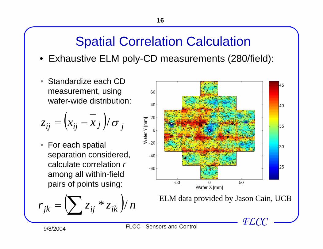
16
FLCC
Spatial Correlation Calculation• Exhaustive ELM poly-CD measurements (280/field):
• Standardize each CD measurement, using wafer-wide distribution:
• For each spatial separation considered, calculate correlation ramong all within-field pairs of points using:
( ) nzzr ikijjk /*∑=
( ) jjijij xxz σ/−=
ELM data provided by Jason Cain, UCB

9/8/2004 FLCC - Sensors and Control
17
FLCC
Impact of Correlation on Delay Variability• Assuming n indep. random variables with equal mean
and variance, the variance of the sum is:
• For ρ = 1, σtot = nσindv
• For ρ = 0, σtot = n1/2σindv
• Potential improvement is factor of n1/2 (i.e., for a 16-stage path, maximum total delay variation reduction is ~4x…)
( )[ ] 2
22
22
)1)((
2
indv
indvnindvtot
nnn
Cn
σρ
σρσσ
−+=
+=Relative Reduction in Delay Variation vs. Correlation between stages, # of stages, with ONLY L_eff varying
0
0.1
0.2
0.3
0.4
0.5
0.6
0.7
0.8
0.9
1
0 0.2 0.4 0.6 0.8 1
Delay Variation, normalized to corr=1 case
Corr
elat
ion
coef
ficie
nt
N=2N=4
N=8N=16

9/8/2004 FLCC - Sensors and Control
18
FLCC
Year 2 MilestonesIntegrated sensor platform development 2 (M26)Gather CMP and etching rate data and correlate with process variables.Zero-footprint Optical Metrology Wafer (Added)Evaluate and calibrate dielectric thickness monitoring (resolution, sensitivity, and stability). Metal etch endpoint and pre-endpoint (<50nm) detection and monitoring. Testing the prototype metrology wafer in vacuum environment.Complete experimental study for CD non-uniformity reducing across the litho-etch sequence (M27)Assess predictive capability of mode, and build optimizing software to compute optimal changes in control parameters. Provide proof of concept test of CD non-uniformity reduction scheme based on direct CD metrology.Aerial Image Metrology (M31)Integrate prototype transducer for use and deployment on a silicon wafer.Using Spatial CD Correlation in IC Design (new)Develop test structures and measurement plans for extracting spatial correlation characteristics.