Embed Size (px)
Citation preview
偉詮電子股份有限公司 Weltrend Semiconductor, Inc.
新竹市科學工業園區工業東九路24號2樓 2F, No. 24, Industry E. 9th RD., Science-Based Industrial Park, Hsin-Chu, Taiwan TEL:886-3-5780241 FAX:886-3-5794278.5770419 Email:[email protected]
`
WT7525
PC POWER SUPPLY SUPERVISOR
Data Sheet
REV. 0.40 Preliminary release
February 21, 2005 The information in this document is subject to change without notice. Weltrend Semiconductor, Inc. All Rights Reserved.
WT7525 Preliminary release Rev. 0.40
Weltrend Semiconductor, Inc. Page 2
GENERAL DESCRIPTION
The WT7525 provides protection circuits, power good output (PGO), fault protection latch (FPOB), and a protection detector function (PSONB) control. It can minimize external components of switching power supply systems in personal computer.
The Over / Under Voltage Detector (OVD / UVD) monitors V33, V5, V12A, V12B and V12C input voltage level. The Over Current Detector (OCD) monitor IS33, IS5, IS12A, IS12B and IS12C input current sense. When OVD or UVD or OCD detect the fault voltage level, the FPOB is latched HIGH and PGO go low. The latch can be reset by PSONB go HIGH. There is 3.5 ms delay time for PSONB turn off FPOB.
When OVD and UVD and OCD detect the right voltage level, the power good output (PGO) will be issue.
FEATURES • The Over/Under Voltage Detector (OVD / UVD) monitors V33, V5, V12A, V12B and V12C input
voltage. • The Over Current Detector (OCD) monitors IS33, IS5, IS12A, IS12B and IS12C input current sense. • Both of the power good output (PGO) and fault protection latch (FPOB) are Open Drain Output. • 75 / 300 ms time delay for UVD. • 300 ms time delay for PGO. • 38 ms for PSONB input signal De–bounce. • 73 us for PGI/OVD/UVD internal signal De–glitches. • 1.2 ms for OCD internal signal De–glitches. • 3.5 ms time delay for PSONB turn-off FPOB.
WT7525 Preliminary release Rev. 0.40
Weltrend Semiconductor, Inc. Page 3
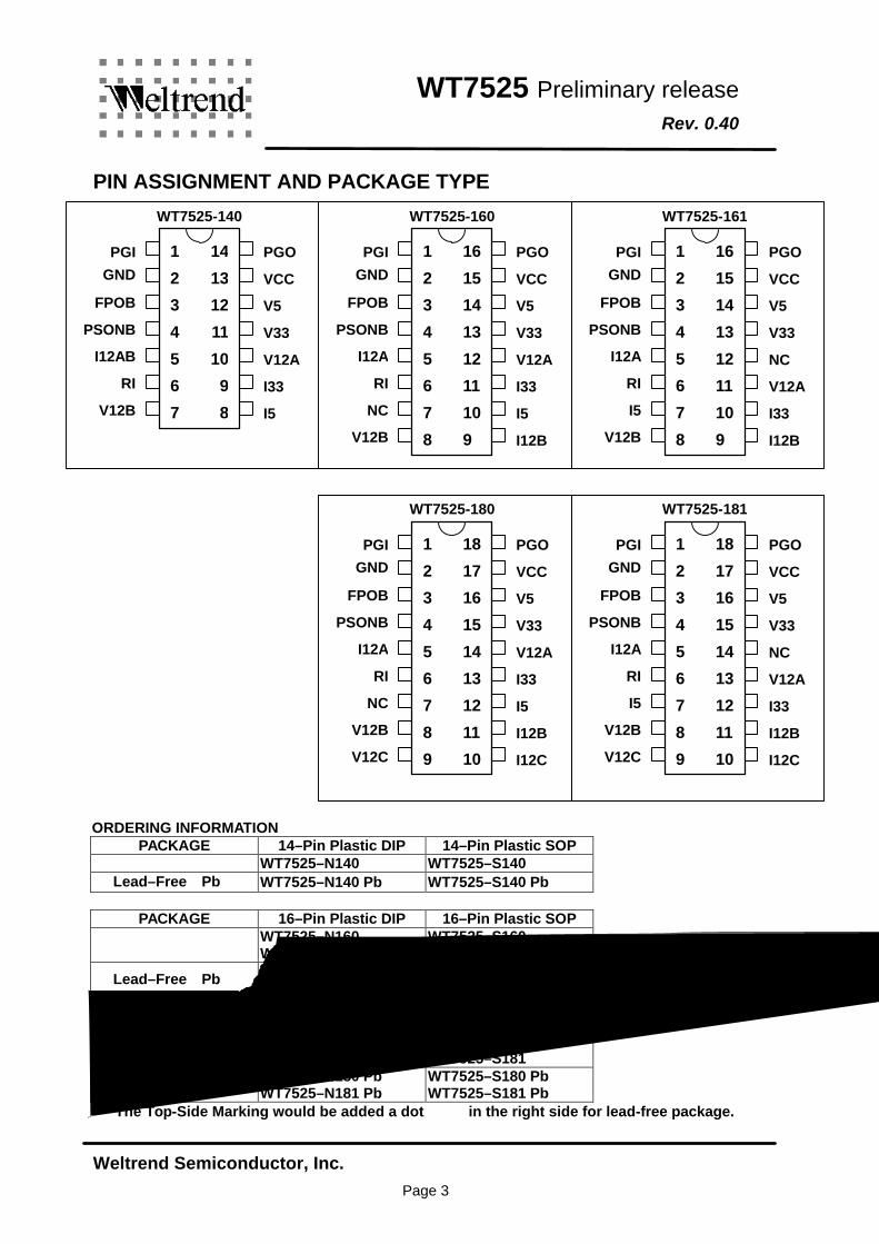
PIN ASSIGNMENT AND PACKAGE TYPE
ORDERING INFORMATION PACKAGE 14–Pin Plastic DIP 14–Pin Plastic SOP
WT7525–N140 WT7525–S140 Lead–Free(Pb) WT7525–N140 Pb WT7525–S140 Pb
PACKAGE 16–Pin Plastic DIP 16–Pin Plastic SOP
WT7525–N160 WT7525–N161
WT7525–S160 WT7525–S161
Lead–Free(Pb) WT7525–N160 Pb WT7525–N161 Pb
WT7525–S160 Pb WT7525–S161 Pb
PACKAGE 18–Pin Plastic DIP 18–Pin Plastic SOP
WT7525–N180 WT7525–N181
WT7525–S180 WT7525–S181
Lead–Free(Pb) WT7525–N180 Pb WT7525–N181 Pb
WT7525–S180 Pb WT7525–S181 Pb
※ The Top-Side Marking would be added a dot(●)in the right side for lead-free package.
PGI
GND
FPOB
PSONB
I12A
RI
NC
V12B
PGO
VCC
V5
V33
V12A
I33
I5
I12B
16
15
14
13
12
11
10
9
1
2
3
4
5
6
7
8
WT7525-160
PGI
GND
FPOB
PSONB
I12AB
RI
V12B
PGO
VCC
V5
V33
V12A
I33
I5
14
13
12
11
10
9
8
1
2
3
4
5
6
7
WT7525-140
PGI
GND
FPOB
PSONB
I12A
RI
I5
V12B
PGO
VCC
V5
V33
NC
V12A
I33
I12B
16
15
14
13
12
11
10
9
1
2
3
4
5
6
7
8
WT7525-161
PGI
GND
FPOB
PSONB
I12A
RI
I5
V12B
V12C
PGO
VCC
V5
V33
NC
V12A
I33
I12B
I12C
18
17
16
15
14
13
12
11
10
1
2
3
4
5
6
7
8
9
WT7525-181
PGI
GND
FPOB
PSONB
I12A
RI
NC
V12B
V12C
PGO
VCC
V5
V33
V12A
I33
I5
I12B
I12C
18
17
16
15
14
13
12
11
10
1
2
3
4
5
6
7
8
9
WT7525-180
WT7525 Preliminary release Rev. 0.40
Weltrend Semiconductor, Inc. Page 4
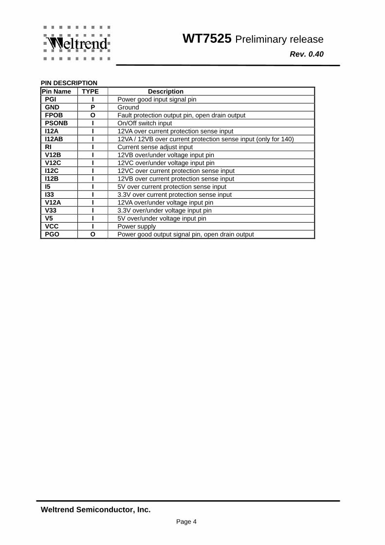
PIN DESCRIPTION Pin Name TYPE Description PGI I Power good input signal pin GND P Ground FPOB O Fault protection output pin, open drain output PSONB I On/Off switch input I12A I 12VA over current protection sense input I12AB I 12VA / 12VB over current protection sense input (only for 140) RI I Current sense adjust input V12B I 12VB over/under voltage input pin V12C I 12VC over/under voltage input pin I12C I 12VC over current protection sense input I12B I 12VB over current protection sense input I5 I 5V over current protection sense input I33 I 3.3V over current protection sense input V12A I 12VA over/under voltage input pin V33 I 3.3V over/under voltage input pin V5 I 5V over/under voltage input pin VCC I Power supply PGO O Power good output signal pin, open drain output
WT7525 Preliminary release Rev. 0.40
Weltrend Semiconductor, Inc. Page 5
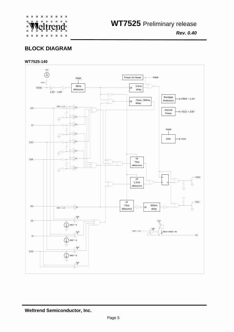
BLOCK DIAGRAM WT7525-140
R
S Q
+-
+-
+-
+-
+-
+-
+-
+-
+-
+-
+-
+-
+-
+-
VCC
VCCI
PSONB
V33
V5
V12A
V12B
FPOB
PGO
PGI
I33
RII5
I12AB
WT7525C-140 BLOCK DIAGRAM
1.2ms
delay75ms / 300msclr
3.5ms
Power On Reset
clrdelay
PWR
clr
debounce
clr73us
debounce
VREF = 1.2V UN
1.2V ~ 1.8V
300msclr
clr73us
debounce delay
38ms
IREF * 8
IREF * 8
IREF * 8
V12A
V12A
V12A
V12A
VREF = 1.2V
VREF = 1.2V
V12A
IREF=VREF / RI
V12A
UN
OV
Power
Reference
Internal
Bandgap
OSC
PWR
CLK
VCCI = 3.6V
VREF = 1.2V
PWR
debounce
UN
UN
OV
UN
OV
OV
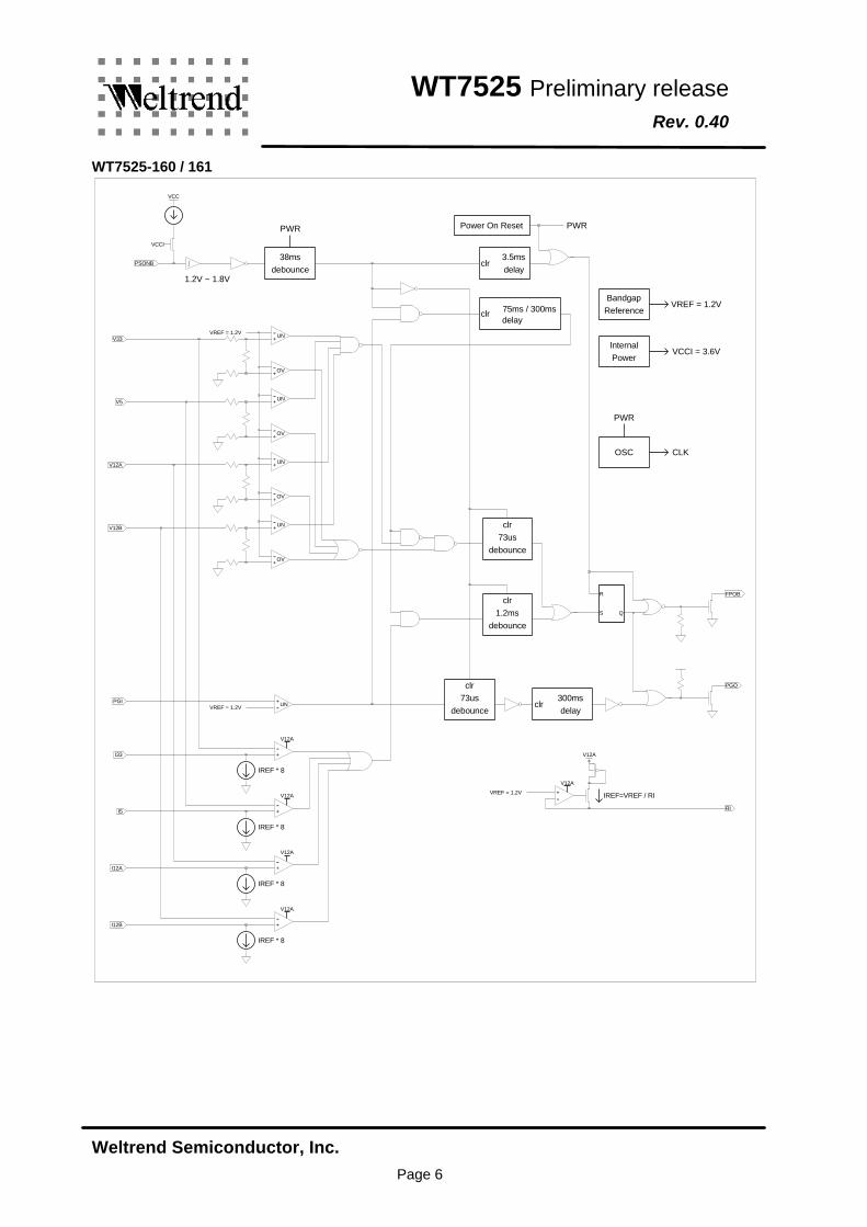
WT7525 Preliminary release Rev. 0.40
Weltrend Semiconductor, Inc. Page 6
WT7525-160 / 161
R
S Q
+-
+-
+-
+-
+-
+-
+-
+-
+-
+-
+-
+-
+-
+-
VCC
VCCI
PSONB
V33
V5
V12A
V12B
FPOB
PGO
PGI
I33
RII5
I12A
I12B
1.2ms
WT7525C-160 BLOCK DIAGRAM
IREF * 8
IREF * 8
delay75ms / 300msclr
3.5ms
Power On Reset
clrdelay
PWR
clr
debounce
clr73us
debounce
VREF = 1.2V UN
1.2V ~ 1.8V
300msclr
clr73us
debounce delay
38ms
IREF * 8
IREF * 8
V12A
V12A
V12A
V12A
VREF = 1.2V
VREF = 1.2V
V12A
IREF=VREF / RI
V12A
UN
OV
Power
Reference
Internal
Bandgap
OSC
PWR
CLK
VCCI = 3.6V
VREF = 1.2V
PWR
debounce
UN
UN
OV
UN
OV
OV
WT7525 Preliminary release Rev. 0.40
Weltrend Semiconductor, Inc. Page 7
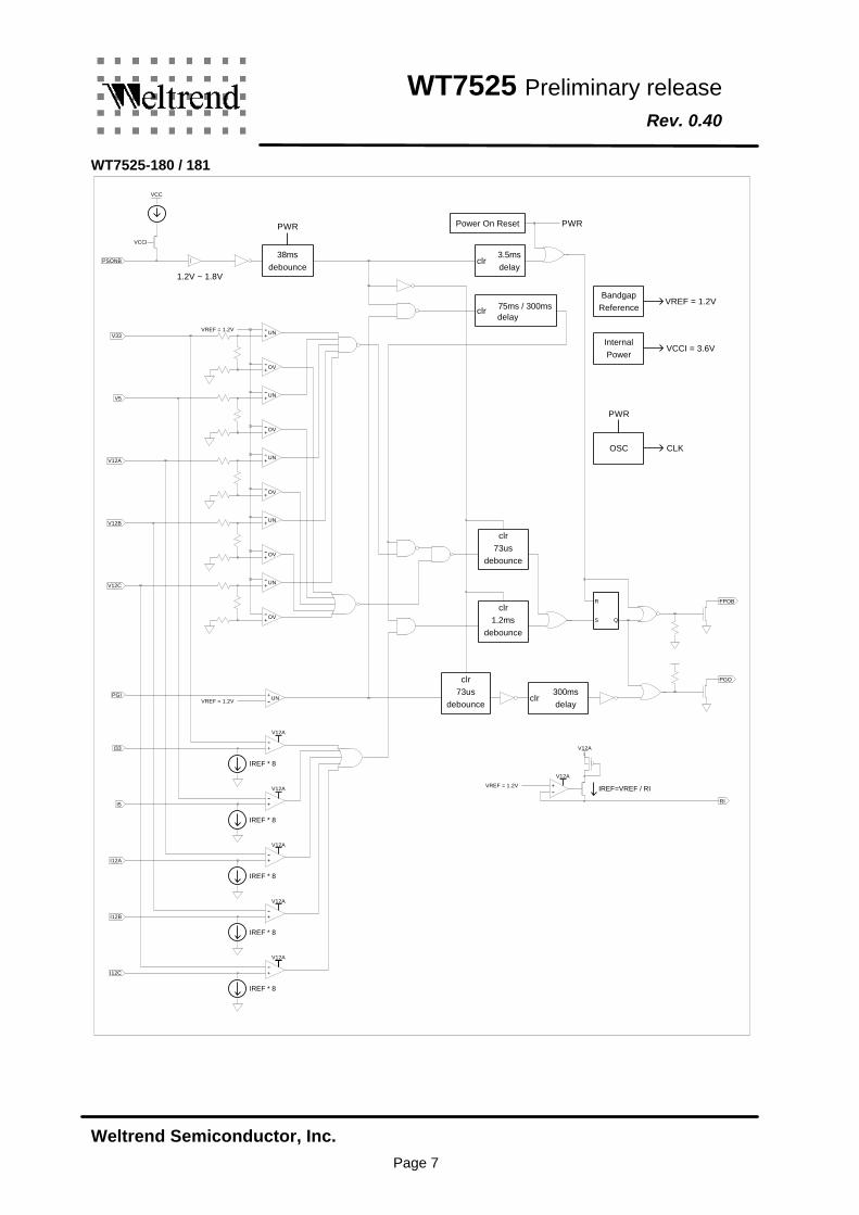
WT7525-180 / 181
R
S Q
+-
+-
+-
+-
+-
+-
+-
+-
+-
+-
+-
+-
+-
+-
+-
+-
+-
VCC
VCCI
PSONB
V33
V5
V12A
V12B
V12C
FPOB
PGO
PGI
I33
RII5
I12A
I12B
I12C
clr73us
debounce
1.2msclr
debounce
38ms
PWR
debounce
UN
OV
UN
OV
V12A
IREF * 8
V12A
IREF * 8
IREF * 8
VREF = 1.2V UN
1.2V ~ 1.8V
IREF * 8
IREF * 8
V12A
V12A
V12A
VREF = 1.2V UN
UN
OV
UN
OV
OV
WT7525C-180 BLOCK DIAGRAM
delay75ms / 300msclr
3.5ms
Power On Reset
clrdelay
PWR
300msclr
clr73us
debounce delay
VREF = 1.2V
V12A
IREF=VREF / RI
V12A
Power
Reference
Internal
Bandgap
OSC
PWR
CLK
VCCI = 3.6V
VREF = 1.2V
WT7525 Preliminary release Rev. 0.40
Weltrend Semiconductor, Inc. Page 8
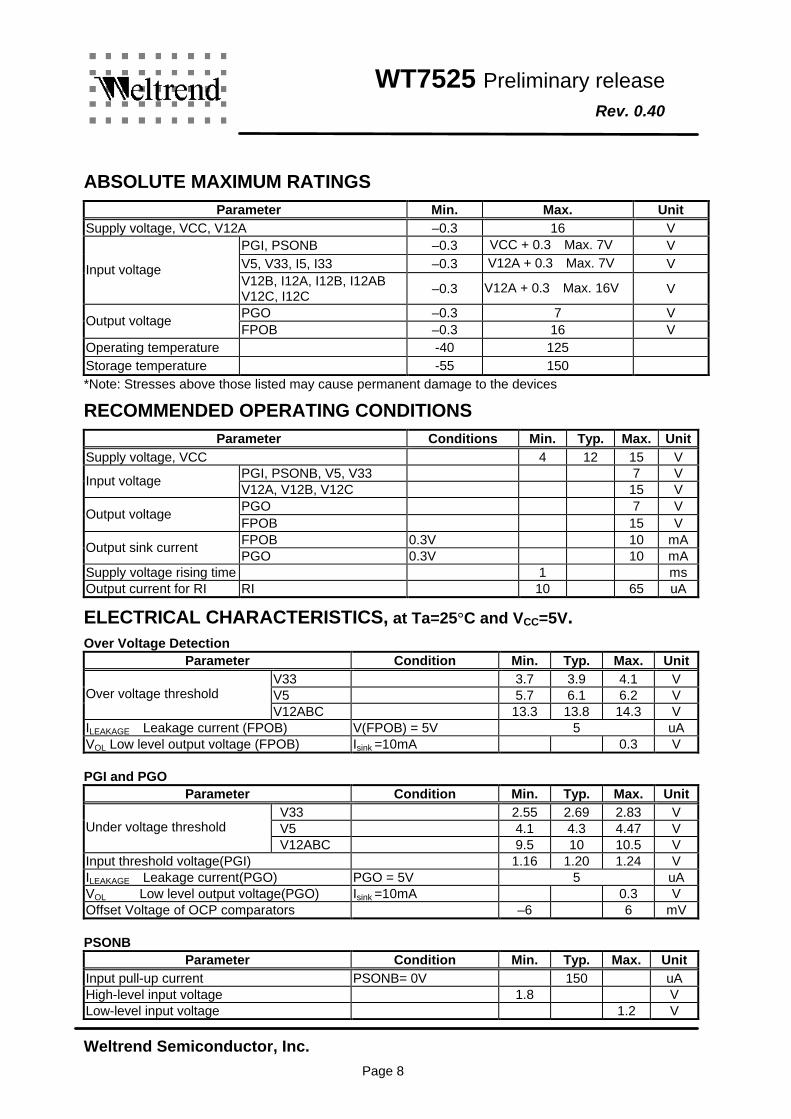
ABSOLUTE MAXIMUM RATINGS Parameter Min. Max. Unit
Supply voltage, VCC, V12A –0.3 16 V PGI, PSONB –0.3 VCC + 0.3(Max. 7V) V V5, V33, I5, I33 –0.3 V12A + 0.3(Max. 7V) V Input voltage V12B, I12A, I12B, I12AB V12C, I12C –0.3 V12A + 0.3(Max. 16V) V
PGO –0.3 7 V Output voltage FPOB –0.3 16 V
Operating temperature -40 125 ℃ Storage temperature -55 150 ℃ *Note: Stresses above those listed may cause permanent damage to the devices
RECOMMENDED OPERATING CONDITIONS Parameter Conditions Min. Typ. Max. Unit
Supply voltage, VCC 4 12 15 V PGI, PSONB, V5, V33 7 V Input voltage V12A, V12B, V12C 15 V PGO 7 V Output voltage FPOB 15 V FPOB 0.3V 10 mA Output sink current PGO 0.3V 10 mA
Supply voltage rising time 1 ms Output current for RI RI 10 65 uA
ELECTRICAL CHARACTERISTICS, at Ta=25°C and VCC=5V. Over Voltage Detection
Parameter Condition Min. Typ. Max. Unit V33 3.7 3.9 4.1 V V5 5.7 6.1 6.2 V Over voltage threshold V12ABC 13.3 13.8 14.3 V
ILEAKAGE Leakage current (FPOB) V(FPOB) = 5V 5 uA VOL Low level output voltage (FPOB) Isink =10mA 0.3 V PGI and PGO
Parameter Condition Min. Typ. Max. Unit V33 2.55 2.69 2.83 V V5 4.1 4.3 4.47 V Under voltage threshold V12ABC 9.5 10 10.5 V
Input threshold voltage(PGI) 1.16 1.20 1.24 V ILEAKAGE Leakage current(PGO) PGO = 5V 5 uA VOL Low level output voltage(PGO) Isink =10mA 0.3 V Offset Voltage of OCP comparators –6 6 mV PSONB
Parameter Condition Min. Typ. Max. Unit Input pull-up current PSONB= 0V 150 uA High-level input voltage 1.8 V Low-level input voltage 1.2 V
WT7525 Preliminary release Rev. 0.40
Weltrend Semiconductor, Inc. Page 9
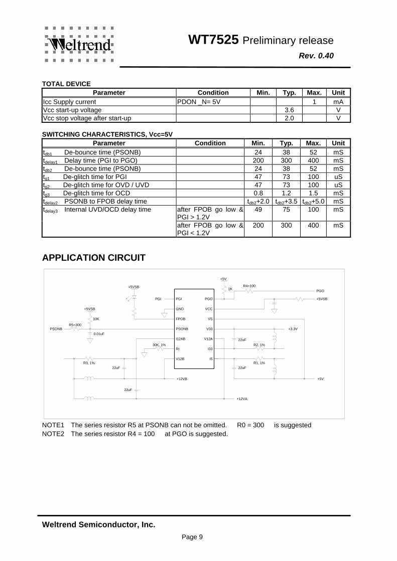
TOTAL DEVICE
Parameter Condition Min. Typ. Max. Unit Icc Supply current PDON _N= 5V 1 mA Vcc start-up voltage 3.6 V Vcc stop voltage after start-up 2.0 V SWITCHING CHARACTERISTICS, Vcc=5V
Parameter Condition Min. Typ. Max. Unit tdb1 De-bounce time (PSONB) 24 38 52 mS tdelay1 Delay time (PGI to PGO) 200 300 400 mS tdb2 De-bounce time (PSONB) 24 38 52 mS tg1 De-glitch time for PGI 47 73 100 uS tg2 De-glitch time for OVD / UVD 47 73 100 uS tg3 De-glitch time for OCD 0.8 1.2 1.5 mS tdelay2 PSONB to FPOB delay time tdb2+2.0 tdb2+3.5 tdb2+5.0 mS
after FPOB go low & PGI > 1.2V
49 75 100 mS tdelay3 Internal UVD/OCD delay time
after FPOB go low & PGI < 1.2V
200 300 400 mS
APPLICATION CIRCUIT
I33
I5
PGI
PSONB
V12A
V33
VCC
VSFPOB
GND
I12AB
PGO
RI
V12BR3, 1%
PGOR4=100
+5VSB
0.01uF
R5=300
10K
+5VSB
PSONB
+12VA
22uF
+12VB
22uF
+5V
R1, 1%22uF
+3.3V
22uFR2, 1%30K, 1%
PGI
+5VSB
+5V
1K
NOTE1:The series resistor R5 at PSONB can not be omitted. (R0 = 300Ω is suggested) NOTE2:The series resistor R4 = 100Ω at PGO is suggested.
WT7525 Preliminary release Rev. 0.40
Weltrend Semiconductor, Inc. Page 10
APPLICATION NOTE
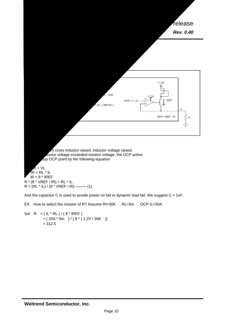
When the current cross inductor raised, inductor voltage raised. And when inductor voltage exceeded resistor voltage, the OCP active. We can setup OCP point by the following equation Let VR = VL R * IR = RL * IL ∵ IR = 8 * IREF R * (8 * VREF / RI) = RL * IL R = (RL * IL) / (8 * VREF / RI) ––––– (1) And the capacitor C is used to avoide power on fail or dynamic load fail. We suggest C > 1uF.
EX:How to select the resistor of R? Assume RI=30KΩ, RL=5mΩ, OCP IL=20A。
Sol:R = ( IL * RL ) / ( 8 * IREF )
= ( 20A * 5mΩ) / { 8 * ( 1.2V / 30KΩ)} = 312.5Ω
WT7525 Preliminary release Rev. 0.40
Weltrend Semiconductor, Inc. Page 11
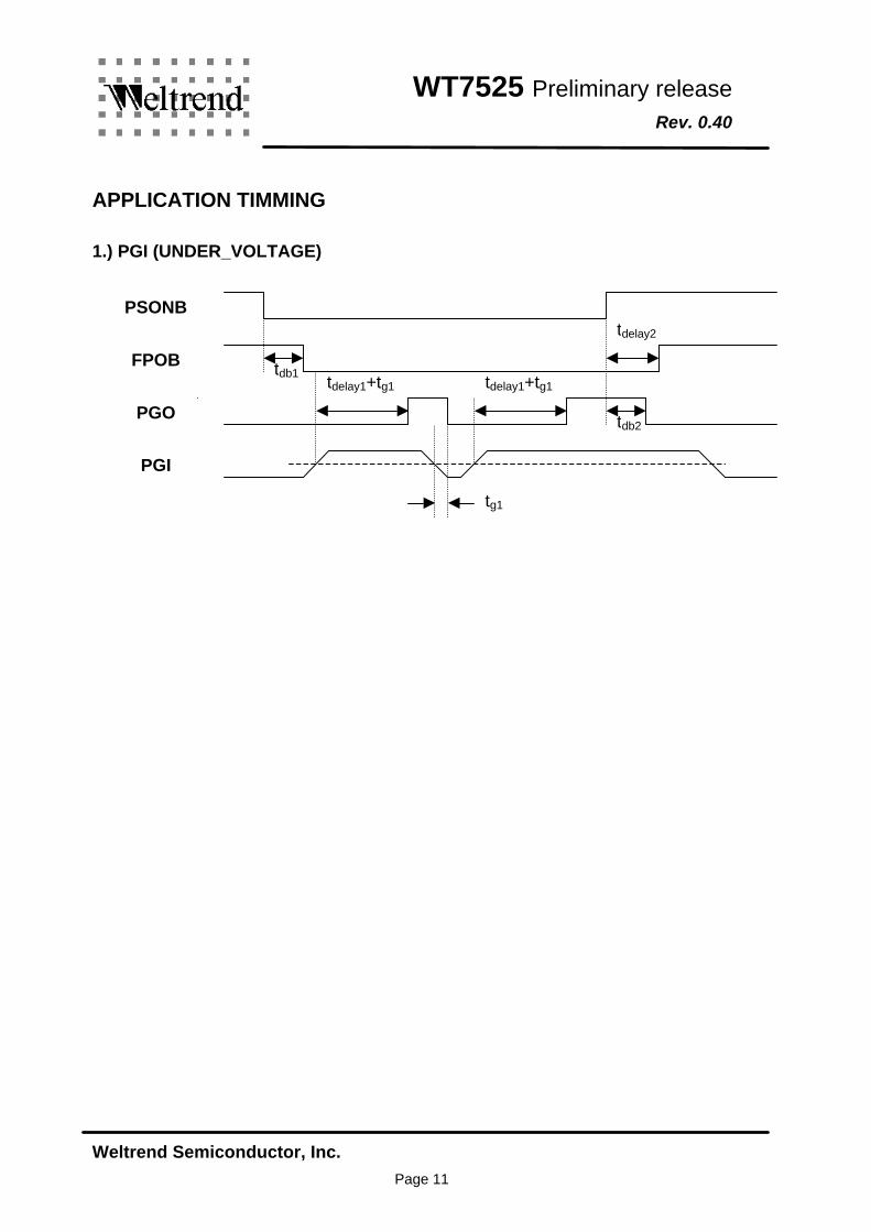
APPLICATION TIMMING 1.) PGI (UNDER_VOLTAGE):
PSONB
FPOB
PGO
PGI
tdb1 tdelay1+tg1
tdb2
tdelay2
tdelay1+tg1
tg1
WT7525 Preliminary release Rev. 0.40
Weltrend Semiconductor, Inc. Page 12
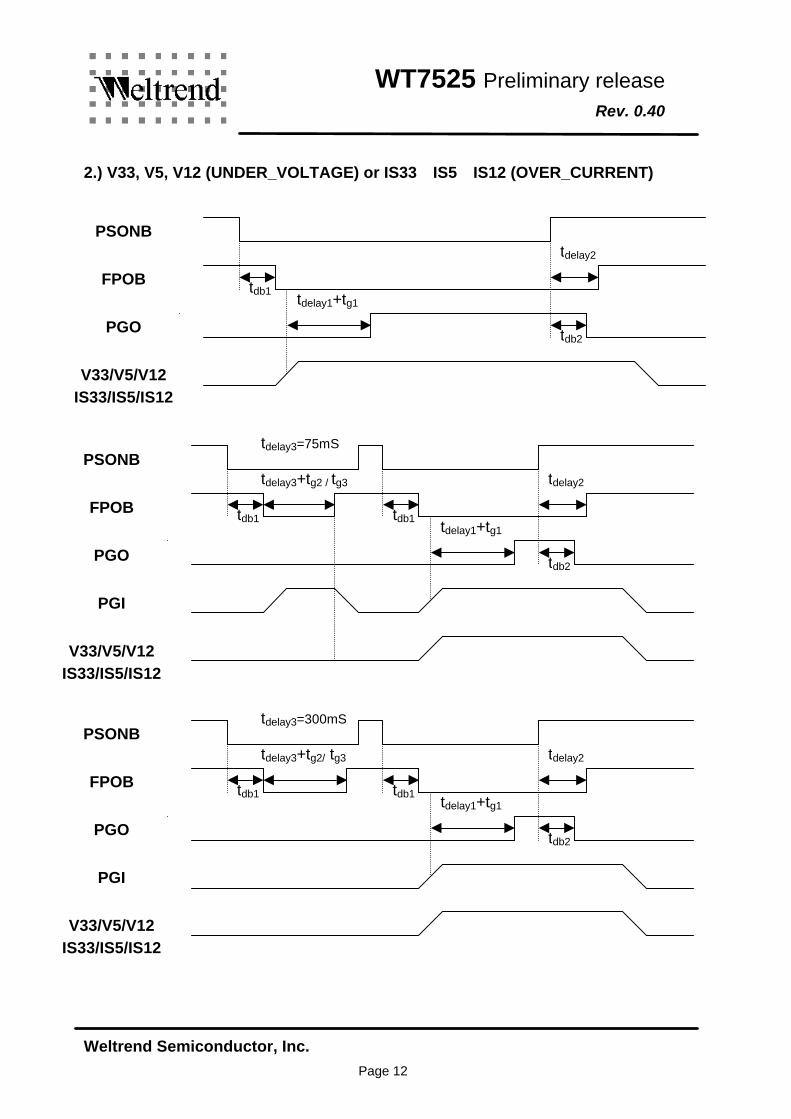
2.) V33, V5, V12 (UNDER_VOLTAGE) or IS33,IS5,IS12 (OVER_CURRENT):
PSONB
FPOB
PGO
V33/V5/V12 IS33/IS5/IS12
tdb1 tdelay1+tg1
tdb2
tdelay2
tdb1 tdelay1+tg1
tdb2
tdelay2 tdelay3+tg2/ tg3
tdb1
PSONB
FPOB
PGO
PGI
V33/V5/V12 IS33/IS5/IS12
tdelay3=300mS
PSONB
FPOB
PGO
PGI
V33/V5/V12 IS33/IS5/IS12
tdb1 tdelay1+tg1
tdb2
tdelay2 tdelay3+tg2 / tg3
tdb1
tdelay3=75mS
WT7525 Preliminary release Rev. 0.40
Weltrend Semiconductor, Inc. Page 13
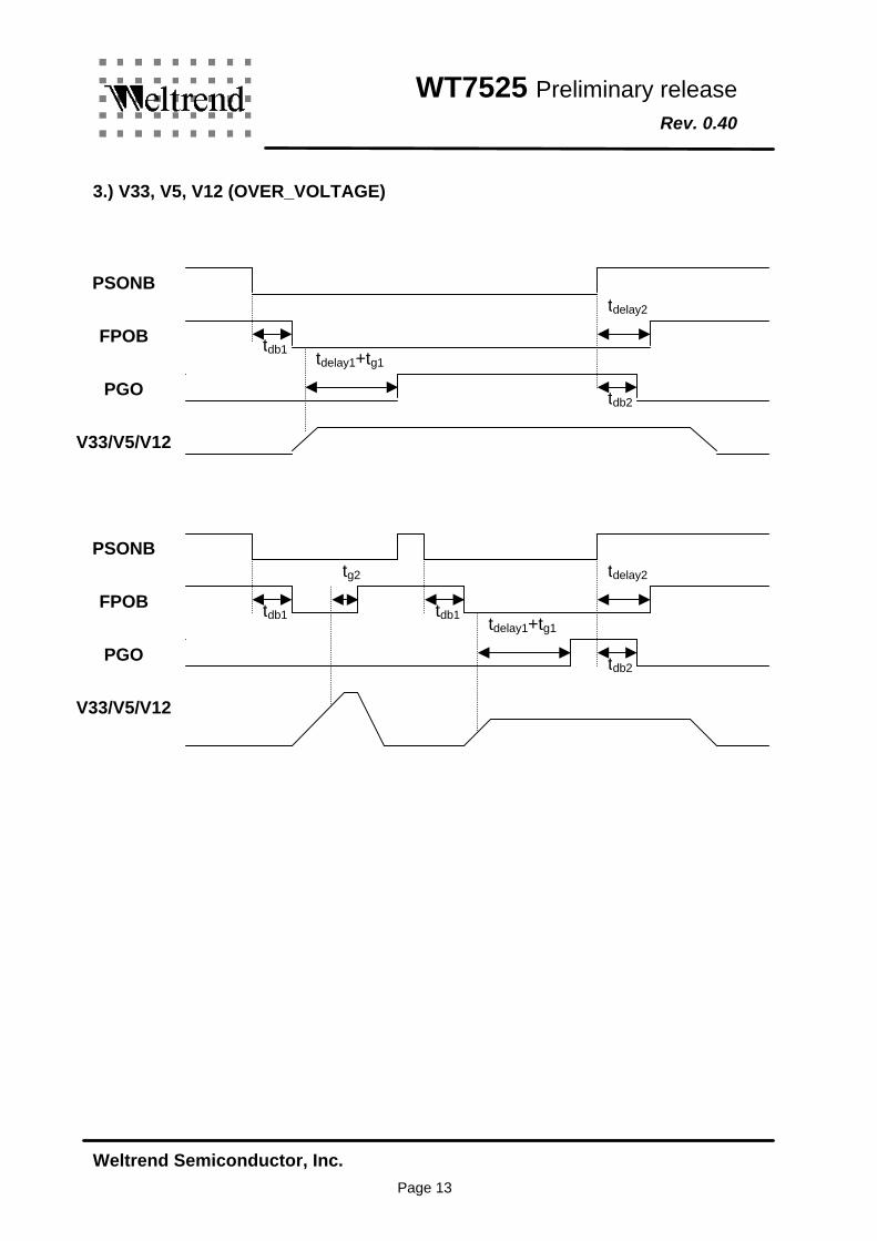
3.) V33, V5, V12 (OVER_VOLTAGE):
PSONB
FPOB
PGO
V33/V5/V12
tdb1 tdelay1+tg1
tdb2
tdelay2
PSONB
FPOB
PGO
V33/V5/V12
tdb1 tdelay1+tg1
tdb2
tdelay2 tg2
tdb1
WT7525 Preliminary release Rev. 0.40
Weltrend Semiconductor, Inc. Page 14
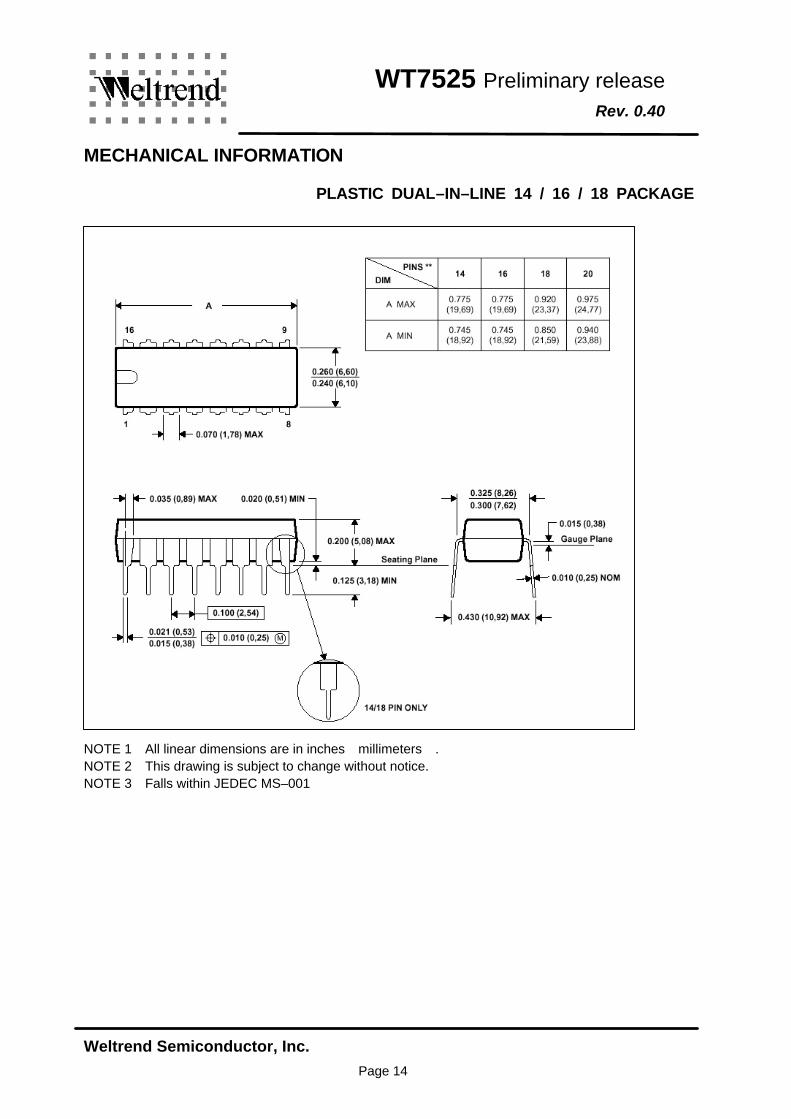
MECHANICAL INFORMATION
PLASTIC DUAL–IN–LINE 14 / 16 / 18 PACKAGE
NOTE 1:All linear dimensions are in inches(millimeters). NOTE 2:This drawing is subject to change without notice. NOTE 3:Falls within JEDEC MS–001
WT7525 Preliminary release Rev. 0.40
Weltrend Semiconductor, Inc. Page 15
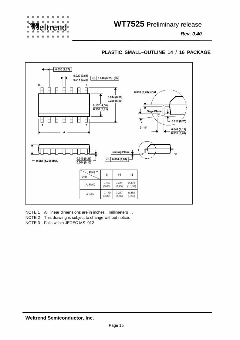
PLASTIC SMALL–OUTLINE 14 / 16 PACKAGE
NOTE 1:All linear dimensions are in inches(millimeters). NOTE 2:This drawing is subject to change without notice. NOTE 3:Falls within JEDEC MS–012
WT7525 Preliminary release Rev. 0.40
Weltrend Semiconductor, Inc. Page 16
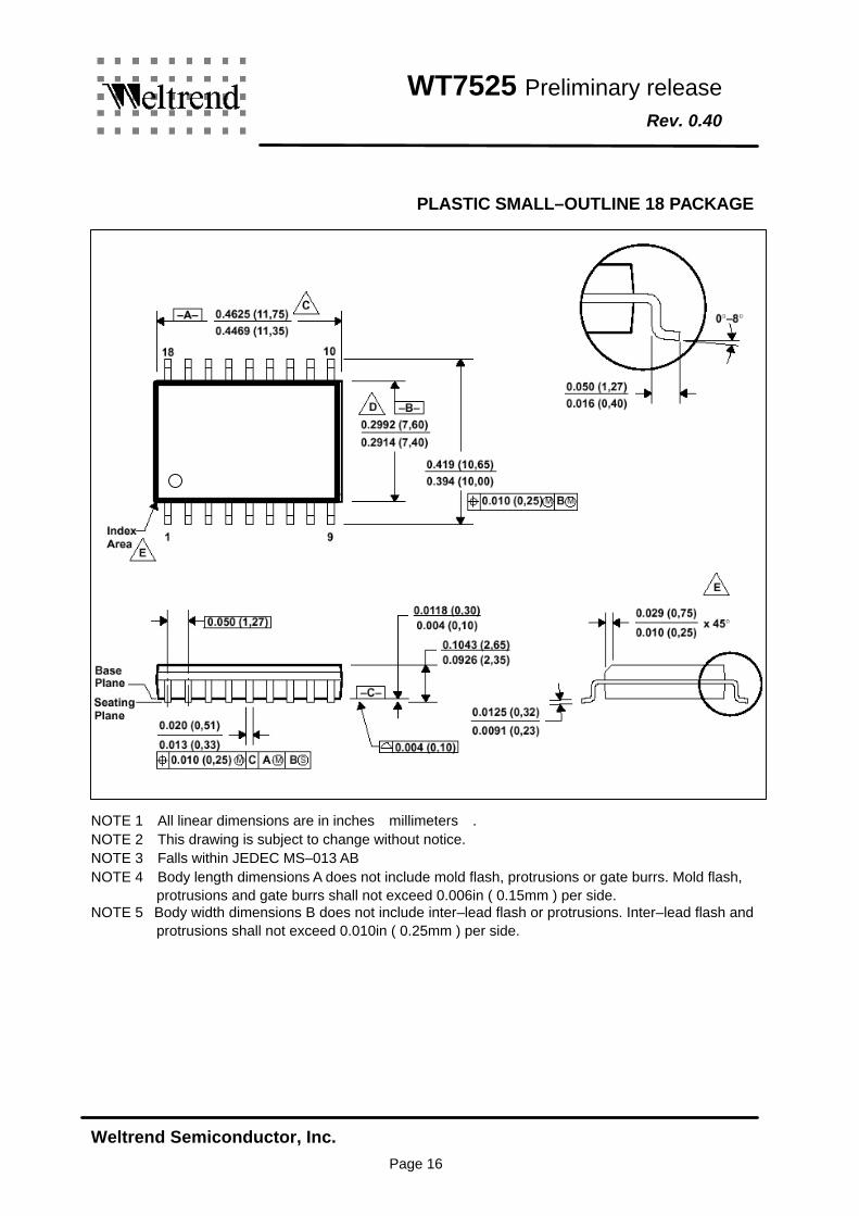
PLASTIC SMALL–OUTLINE 18 PACKAGE NOTE 1:All linear dimensions are in inches(millimeters). NOTE 2:This drawing is subject to change without notice. NOTE 3:Falls within JEDEC MS–013 AB NOTE 4:Body length dimensions A does not include mold flash, protrusions or gate burrs. Mold flash, protrusions and gate burrs shall not exceed 0.006in ( 0.15mm ) per side. NOTE 5:Body width dimensions B does not include inter–lead flash or protrusions. Inter–lead flash and protrusions shall not exceed 0.010in ( 0.25mm ) per side.