Embed Size (px)
Citation preview
1 CHAN PARK, MSE, SNU Spring-2019 Crystal Structure Analyses
X-ray for characterization of thin films
CHAN PARK
Many slides from the ppt made by Bruker, Panalytical, Rigaku and Dr. Scott A. Speakman (prism.mit.edu/xray) were used
2 CHAN PARK, MSE, SNU Spring-2019 Crystal Structure Analyses
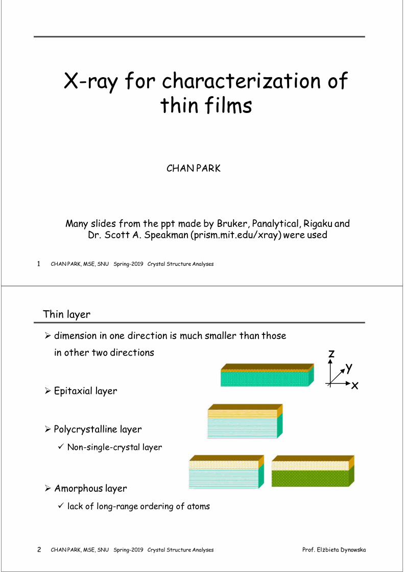
Thin layer
dimension in one direction is much smaller than those
in other two directions
Epitaxial layer
Polycrystalline layer
Non-single-crystal layer
Amorphous layer
lack of long-range ordering of atoms
xy
z
Prof. Elżbieta Dynowska
3 CHAN PARK, MSE, SNU Spring-2019 Crystal Structure Analyses
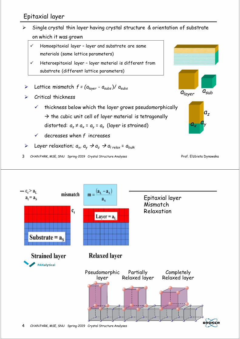
Epitaxial layer
Single crystal thin layer having crystal structure & orientation of substrate
on which it was grown
Homoepitaxial layer – layer and substrate are same
materials (same lattice parameters)
Heteroepitaxial layer – layer material is different from
substrate (different lattice parameters)
Lattice mismatch f = (alayer - asubs )/ asubs
Critical thickness
thickness below which the layer grows pseudomorphically
the cubic unit cell of layer material is tetragonally
distorted: az ≠ ax = ay = as (layer is strained)
decreases when f increases
Layer relaxation; ax, ay az al relax = abulk
alayerasub
ayax
az
Prof. Elżbieta Dynowska
4 CHAN PARK, MSE, SNU Spring-2019 Crystal Structure Analyses
Epitaxial layerMismatchRelaxation
PartiallyRelaxed layer
CompletelyRelaxed layer
Pseudomorphiclayer
5 CHAN PARK, MSE, SNU Spring-2019 Crystal Structure Analyses
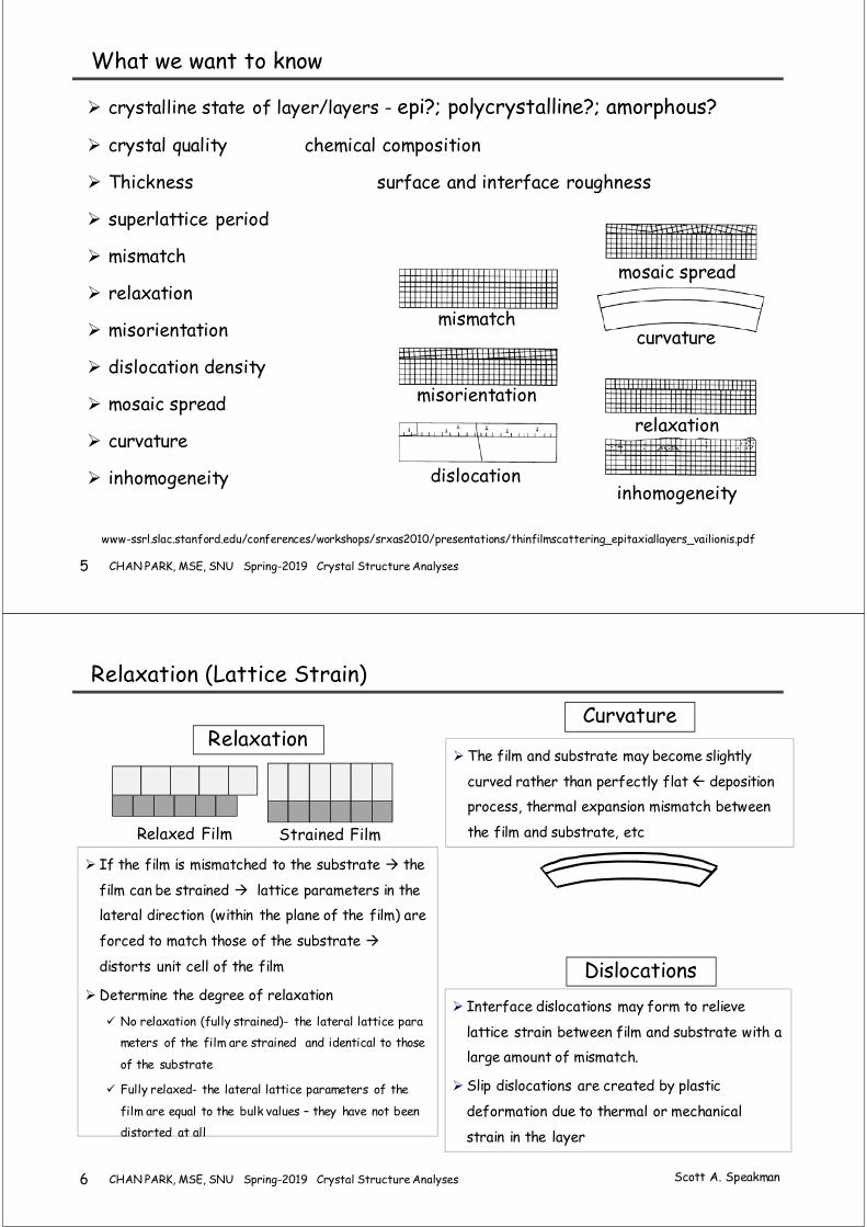
What we want to know
crystalline state of layer/layers - epi?; polycrystalline?; amorphous?
crystal quality chemical composition
Thickness surface and interface roughness
superlattice period
mismatch
relaxation
misorientation
dislocation density
mosaic spread
curvature
inhomogeneity
mismatch
misorientation
dislocation
mosaic spread
curvature
relaxation
inhomogeneity
www-ssrl.slac.stanford.edu/conferences/workshops/srxas2010/presentations/thinfilmscattering_epitaxiallayers_vailionis.pdf
6 CHAN PARK, MSE, SNU Spring-2019 Crystal Structure Analyses
Relaxation (Lattice Strain)
If the film is mismatched to the substrate the
film can be strained lattice parameters in the
lateral direction (within the plane of the film) are
forced to match those of the substrate
distorts unit cell of the film
Determine the degree of relaxation
No relaxation (fully strained)- the lateral lattice para
meters of the film are strained and identical to those
of the substrate
Fully relaxed- the lateral lattice parameters of the
film are equal to the bulk values – they have not been
distorted at all
Relaxed Film Strained Film
Scott A. Speakman
The film and substrate may become slightly
curved rather than perfectly flat deposition
process, thermal expansion mismatch between
the film and substrate, etc
Interface dislocations may form to relieve
lattice strain between film and substrate with a
large amount of mismatch.
Slip dislocations are created by plastic
deformation due to thermal or mechanical
strain in the layer
Curvature
Dislocations
Relaxation
7 CHAN PARK, MSE, SNU Spring-2019 Crystal Structure Analyses
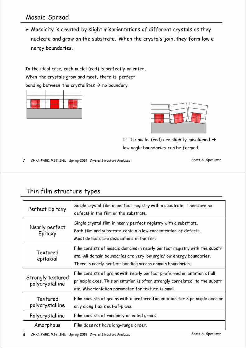
Mosaic Spread
Mosaicity is created by slight misorientations of different crystals as they
nucleate and grow on the substrate. When the crystals join, they form low e
nergy boundaries.
In the ideal case, each nuclei (red) is perfectly oriented.
When the crystals grow and meet, there is perfect
bonding between the crystallites no boundary
If the nuclei (red) are slightly misaligned
low angle boundaries can be formed.
Scott A. Speakman
8 CHAN PARK, MSE, SNU Spring-2019 Crystal Structure Analyses
Thin film structure types
Perfect EpitaxySingle crystal film in perfect registry with a substrate. There are no
defects in the film or the substrate.
Nearly perfect Epitaxy
Single crystal film in nearly perfect registry with a substrate.
Both film and substrate contain a low concentration of defects.
Most defects are dislocations in the film.
Texturedepitaxial
Film consists of mosaic domains in nearly perfect registry with the substr
ate. All domain boundaries are very low angle/low energy boundaries.
There is nearly perfect bonding across domain boundaries.
Strongly textured polycrystalline
Film consists of grains with nearly perfect preferred orientation of all
principle axes. This orientation is often strongly correlated to the substr
ate. Misorientation parameter for texture is small.
Texturedpolycrystalline
Film consists of grains with a preferred orientation for 3 principle axes or
only along 1 axis out-of-plane.
Polycrystalline Film consists of randomly oriented grains.
Amorphous Film does not have long-range order.
Scott A. Speakman
9 CHAN PARK, MSE, SNU Spring-2019 Crystal Structure Analyses
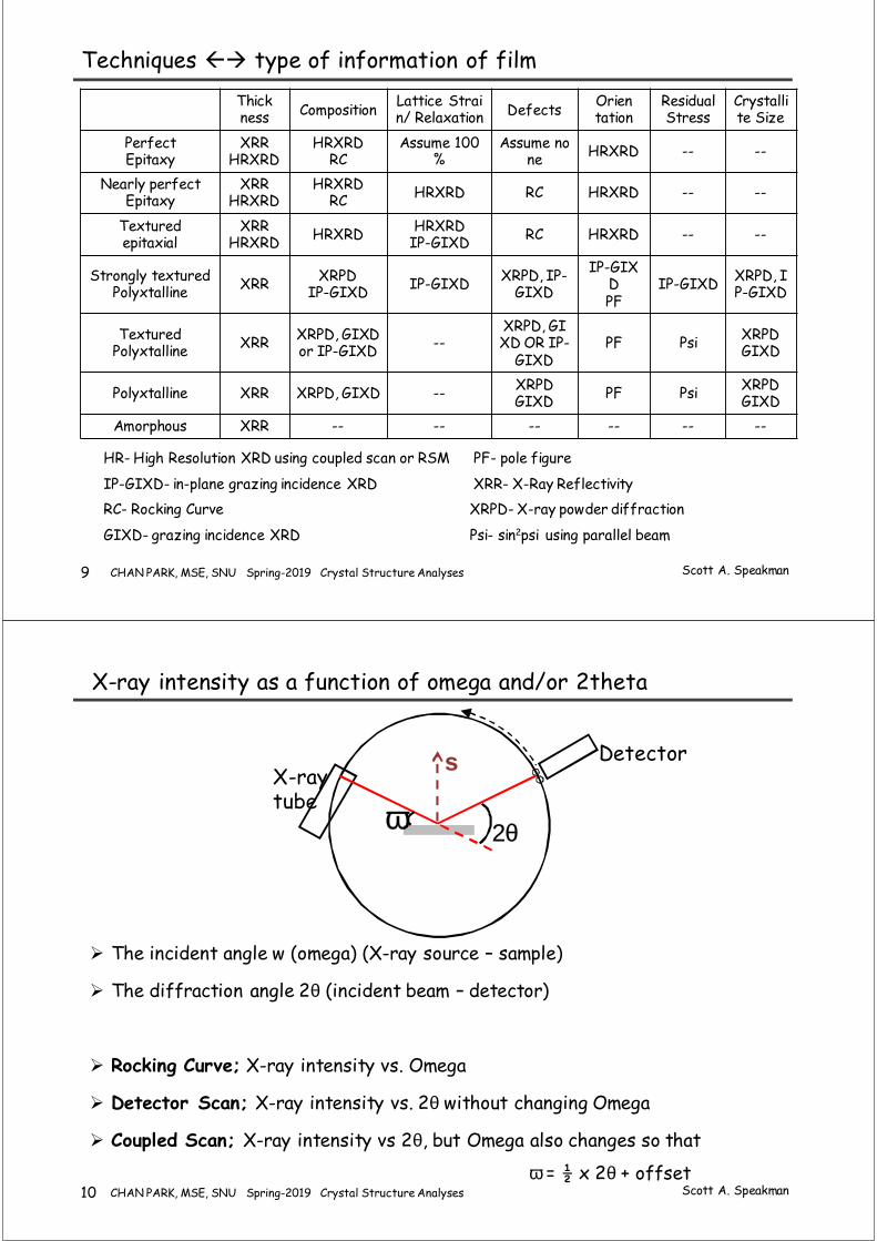
Techniques type of information of film
Thickness Composition Lattice Strai
n/ Relaxation Defects Orientation
ResidualStress
Crystallite Size
PerfectEpitaxy
XRRHRXRD
HRXRDRC
Assume 100%
Assume none HRXRD -- --
Nearly perfect Epitaxy
XRRHRXRD
HRXRDRC HRXRD RC HRXRD -- --
Texturedepitaxial
XRRHRXRD HRXRD HRXRD
IP-GIXD RC HRXRD -- --
Strongly textured Polyxtalline XRR XRPD
IP-GIXD IP-GIXD XRPD, IP-GIXD
IP-GIXDPF
IP-GIXD XRPD, IP-GIXD
TexturedPolyxtalline XRR XRPD, GIXD
or IP-GIXD --XRPD, GIXD OR IP-
GIXDPF Psi XRPD
GIXD
Polyxtalline XRR XRPD, GIXD -- XRPDGIXD PF Psi XRPD
GIXD
Amorphous XRR -- -- -- -- -- --
HR- High Resolution XRD using coupled scan or RSM PF- pole figure
IP-GIXD- in-plane grazing incidence XRD XRR- X-Ray Reflectivity
RC- Rocking Curve XRPD- X-ray powder diffraction
GIXD- grazing incidence XRD Psi- sin2psi using parallel beam
Scott A. Speakman
10 CHAN PARK, MSE, SNU Spring-2019 Crystal Structure Analyses
X-ray intensity as a function of omega and/or 2theta
The incident angle w (omega) (X-ray source – sample)
The diffraction angle 2θ (incident beam – detector)
Rocking Curve; X-ray intensity vs. Omega
Detector Scan; X-ray intensity vs. 2θ without changing Omega
Coupled Scan; X-ray intensity vs 2θ, but Omega also changes so that
ω = ½ x 2θ + offset
ω 2θ
X-raytube
Detectors
Scott A. Speakman
11 CHAN PARK, MSE, SNU Spring-2019 Crystal Structure Analyses
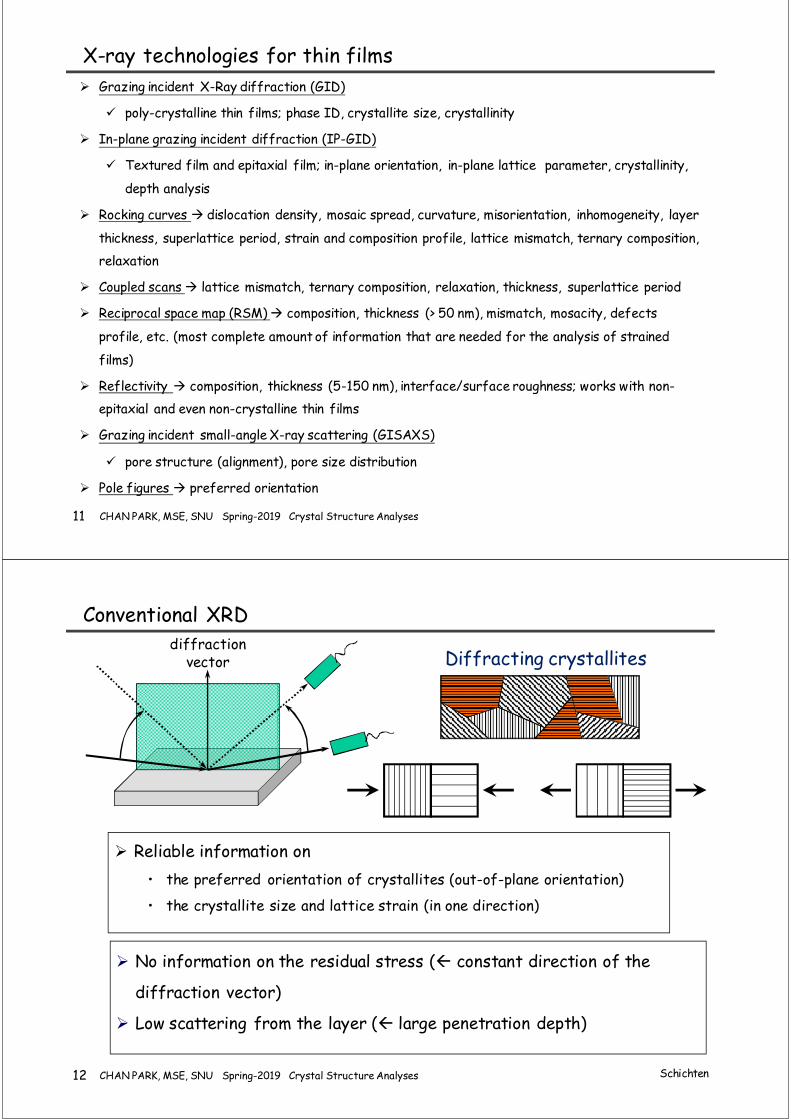
X-ray technologies for thin films Grazing incident X-Ray diffraction (GID)
poly-crystalline thin films; phase ID, crystallite size, crystallinity
In-plane grazing incident diffraction (IP-GID)
Textured film and epitaxial film; in-plane orientation, in-plane lattice parameter, crystallinity,
depth analysis
Rocking curves dislocation density, mosaic spread, curvature, misorientation, inhomogeneity, layer
thickness, superlattice period, strain and composition profile, lattice mismatch, ternary composition,
relaxation
Coupled scans lattice mismatch, ternary composition, relaxation, thickness, superlattice period
Reciprocal space map (RSM) composition, thickness (> 50 nm), mismatch, mosacity, defects
profile, etc. (most complete amount of information that are needed for the analysis of strained
films)
Reflectivity composition, thickness (5-150 nm), interface/surface roughness; works with non-
epitaxial and even non-crystalline thin films
Grazing incident small-angle X-ray scattering (GISAXS)
pore structure (alignment), pore size distribution
Pole figures preferred orientation
12 CHAN PARK, MSE, SNU Spring-2019 Crystal Structure Analyses
Conventional XRD
Reliable information on
• the preferred orientation of crystallites (out-of-plane orientation)
• the crystallite size and lattice strain (in one direction)
Diffracting crystallites
No information on the residual stress ( constant direction of the
diffraction vector)
Low scattering from the layer ( large penetration depth)
Schichten
diffraction vector
13 CHAN PARK, MSE, SNU Spring-2019 Crystal Structure Analyses
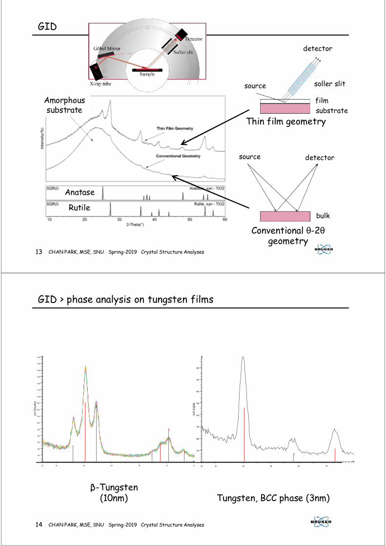
GID
Anatase
Rutile
Amorphous substrate
Conventional θ-2θgeometry
source detector
bulk
Thin film geometry
filmsubstrate
source
detector
soller slit
14 CHAN PARK, MSE, SNU Spring-2019 Crystal Structure Analyses
GID > phase analysis on tungsten films
Lin
(C
ps)
0
100
200
300
400
500
600
700
800
25 30 40 50 60 70
Lin
(C
ounts
)
0
100
200
300
400
500
600
700
800
900
1000
1100
1200
1300
1400
1500
1600
25 30 40 50 60 70 80
β-Tungsten(10nm) Tungsten, BCC phase (3nm)
15 CHAN PARK, MSE, SNU Spring-2019 Crystal Structure Analyses
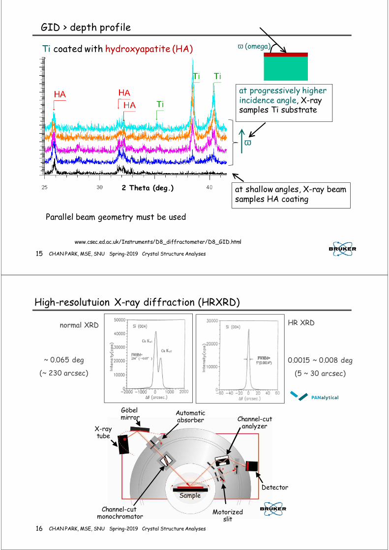
GID > depth profile
at shallow angles, X-ray beam samples HA coating
www.csec.ed.ac.uk/Instruments/D8_diffractometer/D8_GID.html
Ti coated with hydroxyapatite (HA)
Parallel beam geometry must be used
at progressively higher incidence angle, X-ray samples Ti substrate
ω (omega)
ω
2 Theta (deg.)
16 CHAN PARK, MSE, SNU Spring-2019 Crystal Structure Analyses
High-resolutuion X-ray diffraction (HRXRD)
X-raytube
Göbelmirror
Channel-cut monochromator
Sample
Motorizedslit
Detector
Channel-cutanalyzer
Automatic absorber
~ 0.065 deg
(~ 230 arcsec)
0.0015 ~ 0.008 deg
(5 ~ 30 arcsec)
normal XRD HR XRD
17 CHAN PARK, MSE, SNU Spring-2019 Crystal Structure Analyses
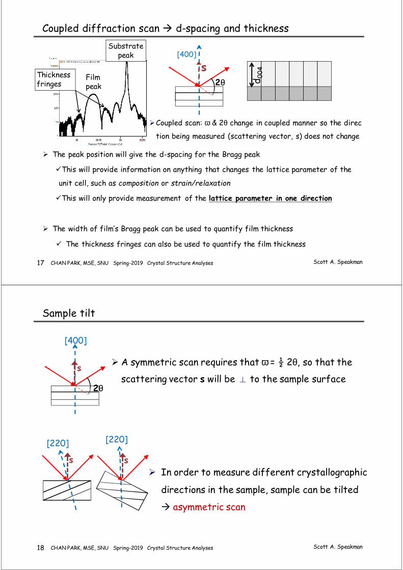
Coupled diffraction scan d-spacing and thickness
The peak position will give the d-spacing for the Bragg peak
This will provide information on anything that changes the lattice parameter of the
unit cell, such as composition or strain/relaxation
This will only provide measurement of the lattice parameter in one direction
The width of film’s Bragg peak can be used to quantify film thickness
The thickness fringes can also be used to quantify the film thickness
2θ
s[400]
d 004
Substrate peak
Film peak
Thickness fringes
Coupled scan: ω & 2θ change in coupled manner so the direc
tion being measured (scattering vector, s) does not change
Scott A. Speakman
18 CHAN PARK, MSE, SNU Spring-2019 Crystal Structure Analyses
Sample tilt
A symmetric scan requires that ω = ½ 2θ, so that the
scattering vector s will be ⊥ to the sample surface2θ
s
[400]
[220]
s
[220]
s
In order to measure different crystallographic
directions in the sample, sample can be tilted
asymmetric scan
Scott A. Speakman
19 CHAN PARK, MSE, SNU Spring-2019 Crystal Structure Analyses
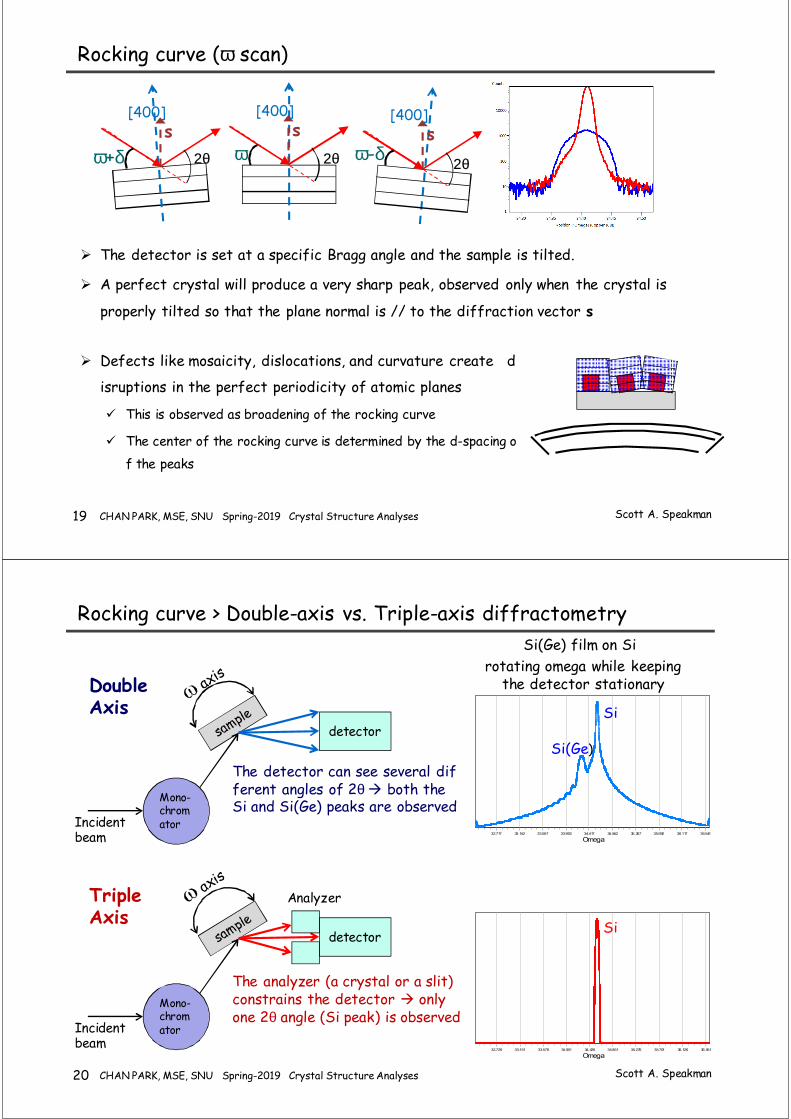
Rocking curve (ω scan)
Defects like mosaicity, dislocations, and curvature create d
isruptions in the perfect periodicity of atomic planes
This is observed as broadening of the rocking curve
The center of the rocking curve is determined by the d-spacing o
f the peaks
The detector is set at a specific Bragg angle and the sample is tilted.
A perfect crystal will produce a very sharp peak, observed only when the crystal is
properly tilted so that the plane normal is // to the diffraction vector s
2θ
s[400]
2θ
s[400]
2θ
s[400]
Scott A. Speakman
ω+δ ω-δω
20 CHAN PARK, MSE, SNU Spring-2019 Crystal Structure Analyses
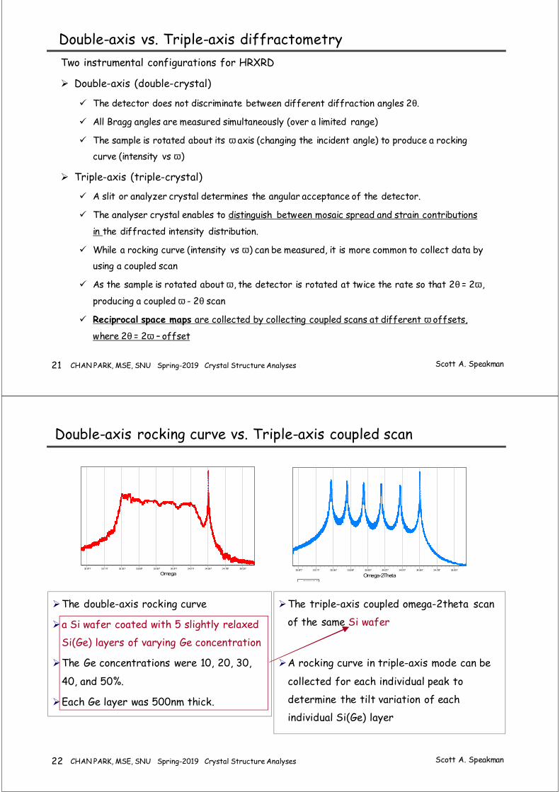
Rocking curve > Double-axis vs. Triple-axis diffractometry
Mono-chromator
detector
Incident beam
Mono-chromator
detector
Incident beam
The detector can see several different angles of 2θ both the Si and Si(Ge) peaks are observed
Analyzer
Omega36.54136.11735.69235.26734.84234.41733.99233.56733.14232.717
Si(Ge)
Si
Omega36.55136.12635.70135.27634.85134.42634.00133.57633.15132.726
Si
The analyzer (a crystal or a slit) constrains the detector only one 2θ angle (Si peak) is observed
Double Axis
Triple Axis
Scott A. Speakman
Si(Ge) film on Si rotating omega while keeping
the detector stationary
21 CHAN PARK, MSE, SNU Spring-2019 Crystal Structure Analyses
Double-axis vs. Triple-axis diffractometryTwo instrumental configurations for HRXRD
Double-axis (double-crystal)
The detector does not discriminate between different diffraction angles 2θ.
All Bragg angles are measured simultaneously (over a limited range)
The sample is rotated about its ω axis (changing the incident angle) to produce a rocking
curve (intensity vs ω)
Triple-axis (triple-crystal)
A slit or analyzer crystal determines the angular acceptance of the detector.
The analyser crystal enables to distinguish between mosaic spread and strain contributions
in the diffracted intensity distribution.
While a rocking curve (intensity vs ω) can be measured, it is more common to collect data by
using a coupled scan
As the sample is rotated about ω , the detector is rotated at twice the rate so that 2θ = 2ω ,
producing a coupled ω - 2θ scan
Reciprocal space maps are collected by collecting coupled scans at different ω offsets,
where 2θ = 2ω – offset
Scott A. Speakman
22 CHAN PARK, MSE, SNU Spring-2019 Crystal Structure Analyses
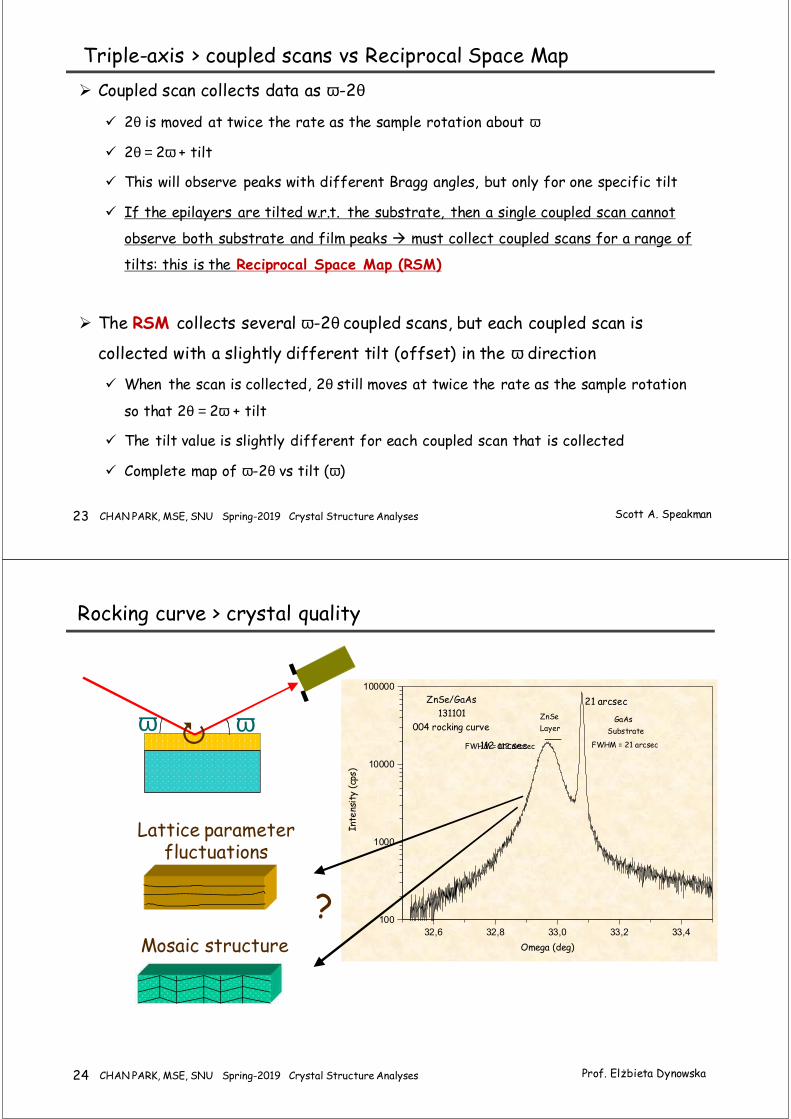
Double-axis rocking curve vs. Triple-axis coupled scan
The double-axis rocking curve
a Si wafer coated with 5 slightly relaxed
Si(Ge) layers of varying Ge concentration
The Ge concentrations were 10, 20, 30,
40, and 50%.
Each Ge layer was 500nm thick.
The triple-axis coupled omega-2theta scan
of the same Si wafer
A rocking curve in triple-axis mode can be
collected for each individual peak to
determine the tilt variation of each
individual Si(Ge) layer
Sim (Sample 1)
Omega-2Theta
35.03734.79734.55734.31734.07733.83733.59733.35733.11732.877
Omega
35.03734.79734.55734.31734.07733.83733.59733.35733.11732.877
Scott A. Speakman
23 CHAN PARK, MSE, SNU Spring-2019 Crystal Structure Analyses
Triple-axis > coupled scans vs Reciprocal Space Map
Coupled scan collects data as ω-2θ
2θ is moved at twice the rate as the sample rotation about ω
2θ = 2ω + tilt
This will observe peaks with different Bragg angles, but only for one specific tilt
If the epilayers are tilted w.r.t. the substrate, then a single coupled scan cannot
observe both substrate and film peaks must collect coupled scans for a range of
tilts: this is the Reciprocal Space Map (RSM)
The RSM collects several ω-2θ coupled scans, but each coupled scan is
collected with a slightly different tilt (offset) in the ω direction
When the scan is collected, 2θ still moves at twice the rate as the sample rotation
so that 2θ = 2ω + tilt
The tilt value is slightly different for each coupled scan that is collected
Complete map of ω-2θ vs tilt (ω)
Scott A. Speakman
24 CHAN PARK, MSE, SNU Spring-2019 Crystal Structure Analyses
Rocking curve > crystal quality
32,6 32,8 33,0 33,2 33,4
100
1000
10000
100000
ZnSe/GaAs 131101004 rocking curve
FWHM = 112 arcsec
ZnSeLayer
FWHM = 21 arcsec
GaAsSubstrate
Omega (deg)
Inte
nsit
y (c
ps)
?
21 arcsec
112 arcsec
Prof. Elżbieta Dynowska
�
Lattice parameter fluctuations
Mosaic structure
ωω
25 CHAN PARK, MSE, SNU Spring-2019 Crystal Structure Analyses
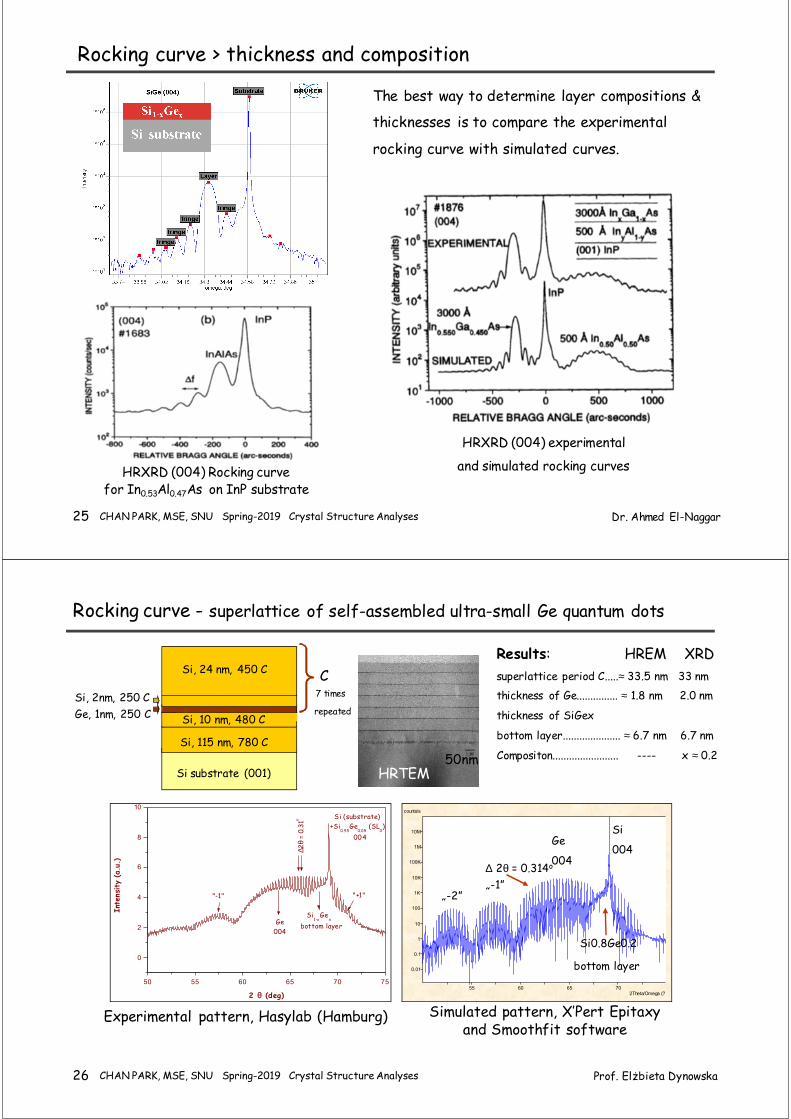
Rocking curve > thickness and composition
HRXRD (004) Rocking curvefor In0.53Al0.47As on InP substrate
Dr. Ahmed El-Naggar
HRXRD (004) experimental
and simulated rocking curves
The best way to determine layer compositions &
thicknesses is to compare the experimental
rocking curve with simulated curves.
26 CHAN PARK, MSE, SNU Spring-2019 Crystal Structure Analyses
50 55 60 65 70 75
0
2
4
6
8
10
∆2θ
= 0.
31o
Si1-x
Gex
bottom layer
"-1" "+1"
Ge004
S i (substrate) +Si
0.95Ge
0.05 (SL
0)
004
Int
ensity
(a.u
.)
2 θ (deg)
Si substrate (001)
Si, 115 nm, 780 C
Si, 10 nm, 480 C
Si, 24 nm, 450 C
Si, 2nm, 250 CGe, 1nm, 250 C
7 times
repeated
55 60 65 702Theta/Omega (?
0.01
0.1
1
10
100
1K
10K
100K
1M
10M
counts/s
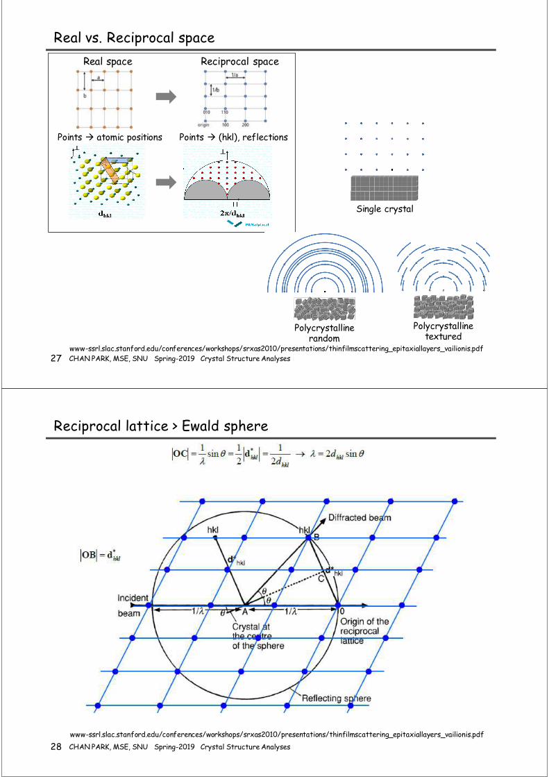
Rocking curve - superlattice of self-assembled ultra-small Ge quantum dots
Experimental pattern, Hasylab (Hamburg) Simulated pattern, X’Pert Epitaxy and Smoothfit software
Si
004Ge
004∆ 2θ = 0.314o
Si0.8Ge0.2
bottom layer
„-1”„-2”
CResults: HREM XRDsuperlattice period C.....≈ 33.5 nm 33 nm
thickness of Ge............... ≈ 1.8 nm 2.0 nm
thickness of SiGex
bottom layer..................... ≈ 6.7 nm 6.7 nm
Compositon........................ ---- x ≈ 0.250nmHRTEM
Prof. Elżbieta Dynowska
27 CHAN PARK, MSE, SNU Spring-2019 Crystal Structure Analyses
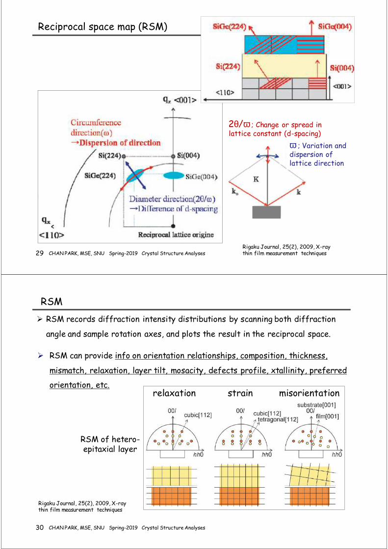
Real vs. Reciprocal space
Real space Reciprocal space
Points atomic positions Points (hkl), reflections
www-ssrl.slac.stanford.edu/conferences/workshops/srxas2010/presentations/thinfilmscattering_epitaxiallayers_vailionis.pdf
Polycrystalline textured
Polycrystalline random
Single crystal
28 CHAN PARK, MSE, SNU Spring-2019 Crystal Structure Analyses
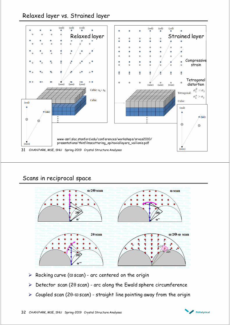
Reciprocal lattice > Ewald sphere
www-ssrl.slac.stanford.edu/conferences/workshops/srxas2010/presentations/thinfilmscattering_epitaxiallayers_vailionis.pdf
29 CHAN PARK, MSE, SNU Spring-2019 Crystal Structure Analyses
Reciprocal space map (RSM)
Rigaku Journal, 25(2), 2009, X-ray thin film measurement techniques
2θ/ω ; Change or spread in lattice constant (d-spacing)
ω ; Variation and dispersion of lattice direction
30 CHAN PARK, MSE, SNU Spring-2019 Crystal Structure Analyses
RSM
RSM records diffraction intensity distributions by scanning both diffraction
angle and sample rotation axes, and plots the result in the reciprocal space.
Rigaku Journal, 25(2), 2009, X-ray thin film measurement techniques
RSM can provide info on orientation relationships, composition, thickness,
mismatch, relaxation, layer tilt, mosacity, defects profile, xtallinity, preferred
orientation, etc.
RSM of hetero-epitaxial layer
relaxation strain misorientation
31 CHAN PARK, MSE, SNU Spring-2019 Crystal Structure Analyses
www-ssrl.slac.stanford.edu/conferences/workshops/srxas2010/presentations/thinfilmscattering_epitaxiallayers_vailionis.pdf
Relaxed layer vs. Strained layer
Strained layerRelaxed layer
Tetragonal distortion
Compressive strain
32 CHAN PARK, MSE, SNU Spring-2019 Crystal Structure Analyses
Scans in reciprocal space
Rocking curve (ω scan) - arc centered on the origin
Detector scan (2θ scan) - arc along the Ewald sphere circumference
Coupled scan (2θ-ω scan) - straight line pointing away from the origin
33 CHAN PARK, MSE, SNU Spring-2019 Crystal Structure Analyses
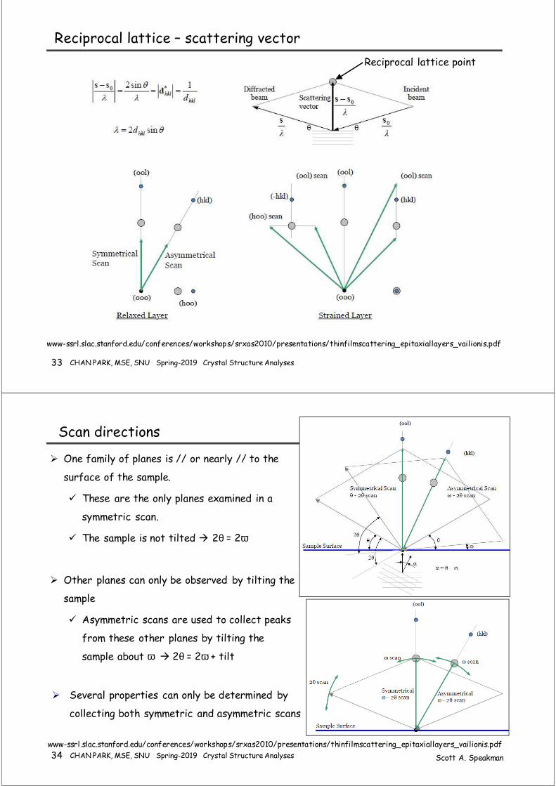
Reciprocal lattice – scattering vector
www-ssrl.slac.stanford.edu/conferences/workshops/srxas2010/presentations/thinfilmscattering_epitaxiallayers_vailionis.pdf
Reciprocal lattice point
34 CHAN PARK, MSE, SNU Spring-2019 Crystal Structure Analyseswww-ssrl.slac.stanford.edu/conferences/workshops/srxas2010/presentations/thinfilmscattering_epitaxiallayers_vailionis.pdf
Scan directions
One family of planes is // or nearly // to the
surface of the sample.
These are the only planes examined in a
symmetric scan.
The sample is not tilted 2θ = 2ω
Other planes can only be observed by tilting the
sample
Asymmetric scans are used to collect peaks
from these other planes by tilting the
sample about ω 2θ = 2ω + tilt
Several properties can only be determined by
collecting both symmetric and asymmetric scans
Scott A. Speakman
35 CHAN PARK, MSE, SNU Spring-2019 Crystal Structure Analyses
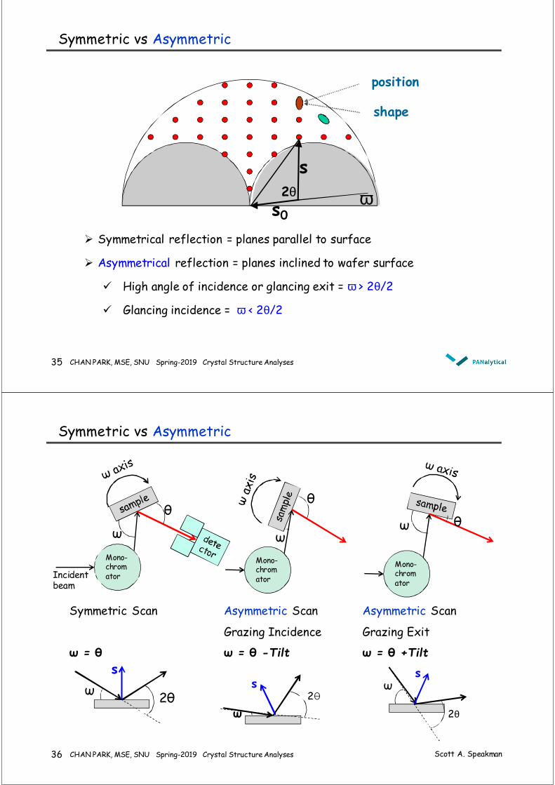
Symmetric vs Asymmetric
Symmetrical reflection = planes parallel to surface
Asymmetrical reflection = planes inclined to wafer surface
High angle of incidence or glancing exit = ω > 2θ/2
Glancing incidence = ω < 2θ/2
shape
s0ω
s2θ
position
36 CHAN PARK, MSE, SNU Spring-2019 Crystal Structure Analyses
Symmetric vs Asymmetric
Mono-chromatorIncident
beam
ω
θ
Symmetric Scan
ω = θ
Mono-chromator
ω
θ
Asymmetric Scan
Grazing Incidence
ω = θ -Tilt
Mono-chromator
ω θ
Asymmetric Scan
Grazing Exit
ω = θ +Tilt
s
ω 2θ
Scott A. Speakman
s
ω
2θ
sω
2θ
37 CHAN PARK, MSE, SNU Spring-2019 Crystal Structure Analyses
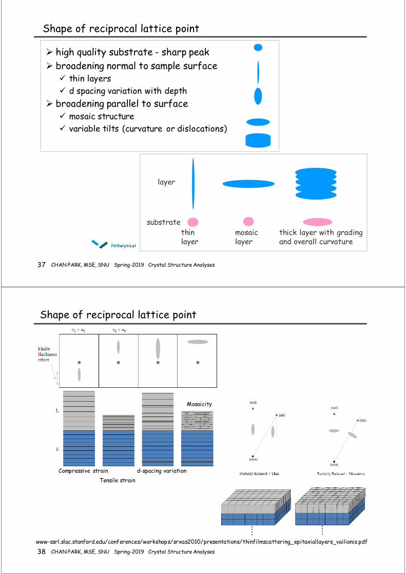
Shape of reciprocal lattice point
high quality substrate - sharp peak broadening normal to sample surface
thin layers d spacing variation with depth
broadening parallel to surface mosaic structure variable tilts (curvature or dislocations)
layer
substratethinlayer
mosaiclayer
thick layer with grading and overall curvature
38 CHAN PARK, MSE, SNU Spring-2019 Crystal Structure Analyses
Shape of reciprocal lattice point
www-ssrl.slac.stanford.edu/conferences/workshops/srxas2010/presentations/thinfilmscattering_epitaxiallayers_vailionis.pdf
Compressive strain
Tensile strain
d-spacing variation
Mosaicity
39 CHAN PARK, MSE, SNU Spring-2019 Crystal Structure Analyses
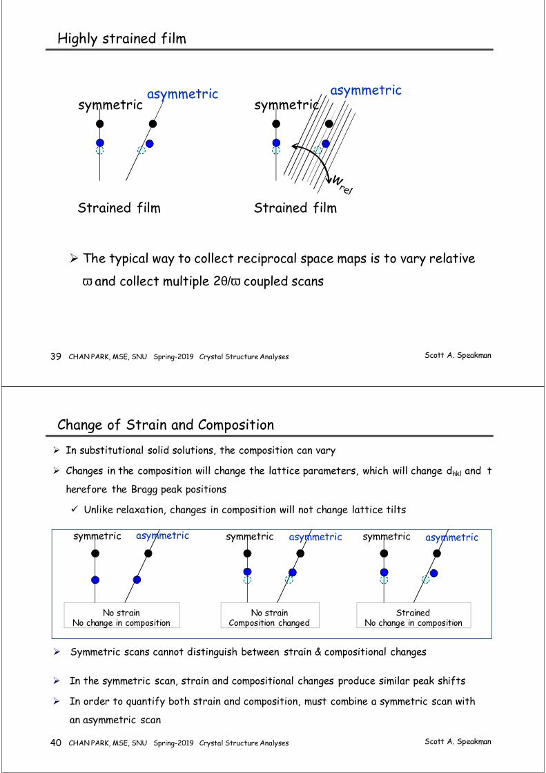
Highly strained film
The typical way to collect reciprocal space maps is to vary relative
ω and collect multiple 2θ/ω coupled scans
Strained film
symmetricasymmetric
Strained film
symmetricasymmetric
Scott A. Speakman
40 CHAN PARK, MSE, SNU Spring-2019 Crystal Structure Analyses
Change of Strain and Composition
In substitutional solid solutions, the composition can vary
Changes in the composition will change the lattice parameters, which will change dhkl and t
herefore the Bragg peak positions
Unlike relaxation, changes in composition will not change lattice tilts
No strainNo change in composition
No strainComposition changed
StrainedNo change in composition
symmetric asymmetric symmetric asymmetric symmetric asymmetric
Scott A. Speakman
In the symmetric scan, strain and compositional changes produce similar peak shifts
In order to quantify both strain and composition, must combine a symmetric scan with
an asymmetric scan
Symmetric scans cannot distinguish between strain & compositional changes
41 CHAN PARK, MSE, SNU Spring-2019 Crystal Structure Analyses
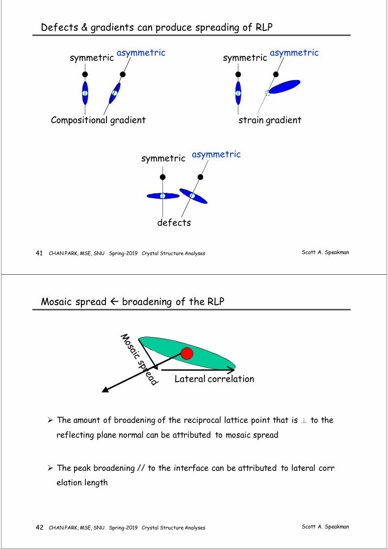
Defects & gradients can produce spreading of RLP
Compositional gradient
symmetric asymmetric
strain gradient
symmetric asymmetric
defects
symmetric asymmetric
Scott A. Speakman
42 CHAN PARK, MSE, SNU Spring-2019 Crystal Structure Analyses
Mosaic spread broadening of the RLP
The amount of broadening of the reciprocal lattice point that is ⊥ to the
reflecting plane normal can be attributed to mosaic spread
The peak broadening // to the interface can be attributed to lateral corr
elation length
Lateral correlation
Scott A. Speakman
43 CHAN PARK, MSE, SNU Spring-2019 Crystal Structure Analyses
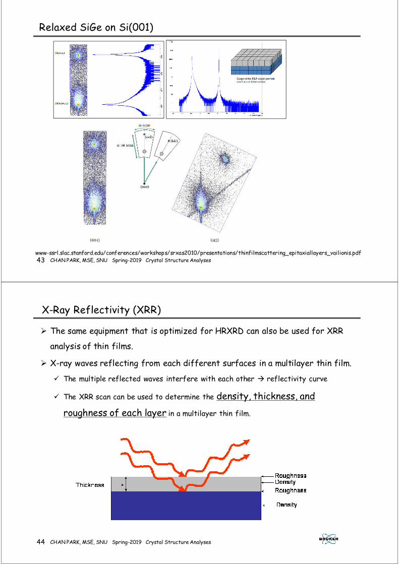
Relaxed SiGe on Si(001)
www-ssrl.slac.stanford.edu/conferences/workshops/srxas2010/presentations/thinfilmscattering_epitaxiallayers_vailionis.pdf
44 CHAN PARK, MSE, SNU Spring-2019 Crystal Structure Analyses
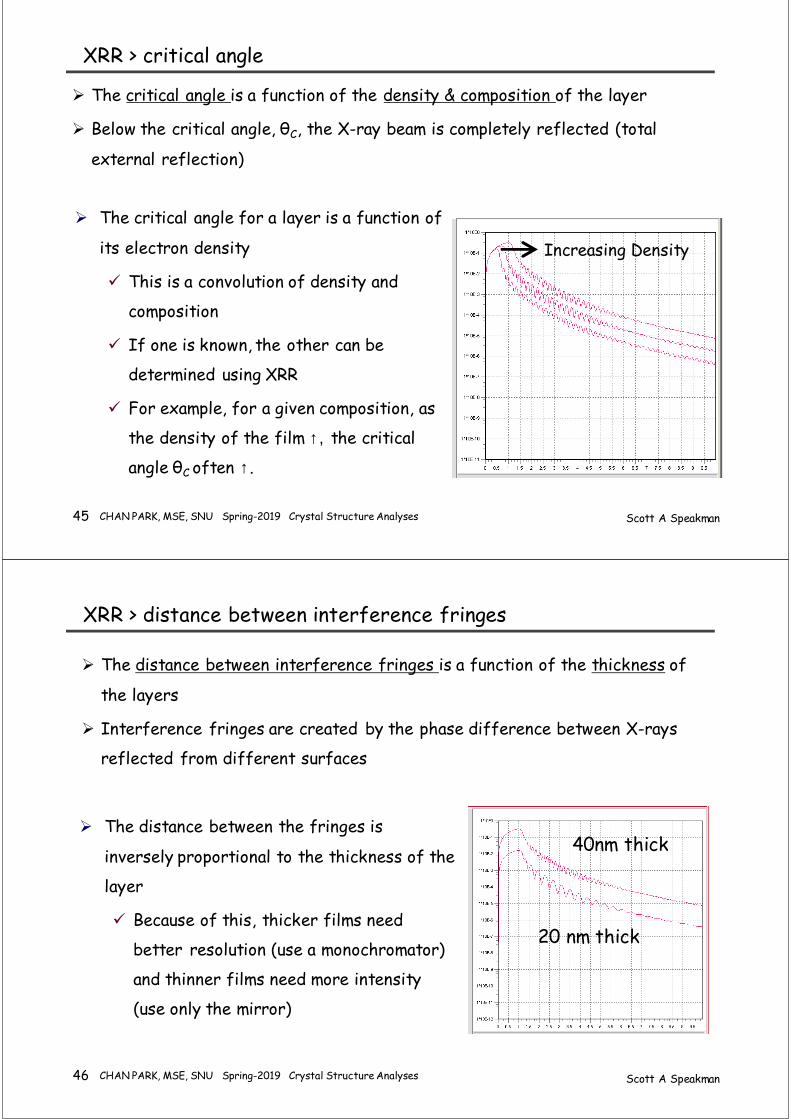
X-Ray Reflectivity (XRR)
The same equipment that is optimized for HRXRD can also be used for XRR
analysis of thin films.
X-ray waves reflecting from each different surfaces in a multilayer thin film.
The multiple reflected waves interfere with each other reflectivity curve
The XRR scan can be used to determine the density, thickness, and
roughness of each layer in a multilayer thin film.
45 CHAN PARK, MSE, SNU Spring-2019 Crystal Structure Analyses
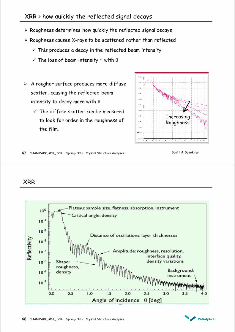
XRR > critical angle
The critical angle is a function of the density & composition of the layer
Below the critical angle, θC, the X-ray beam is completely reflected (total
external reflection)
Increasing Density
The critical angle for a layer is a function of
its electron density
This is a convolution of density and
composition
If one is known, the other can be
determined using XRR
For example, for a given composition, as
the density of the film ↑, the critical
angle θC often ↑.
Scott A Speakman
46 CHAN PARK, MSE, SNU Spring-2019 Crystal Structure Analyses
XRR > distance between interference fringes
The distance between interference fringes is a function of the thickness of
the layers
Interference fringes are created by the phase difference between X-rays
reflected from different surfaces
The distance between the fringes is
inversely proportional to the thickness of the
layer
Because of this, thicker films need
better resolution (use a monochromator)
and thinner films need more intensity
(use only the mirror)
40nm thick
20 nm thick
Scott A Speakman
47 CHAN PARK, MSE, SNU Spring-2019 Crystal Structure Analyses
XRR > how quickly the reflected signal decays
Roughness determines how quickly the reflected signal decays
Roughness causes X-rays to be scattered rather than reflected
This produces a decay in the reflected beam intensity
The loss of beam intensity ↑ with θ
Scott A Speakman
A rougher surface produces more diffuse
scatter, causing the reflected beam
intensity to decay more with θ
The diffuse scatter can be measured
to look for order in the roughness of
the film.
Increasing Roughness
48 CHAN PARK, MSE, SNU Spring-2019 Crystal Structure Analyses
XRR
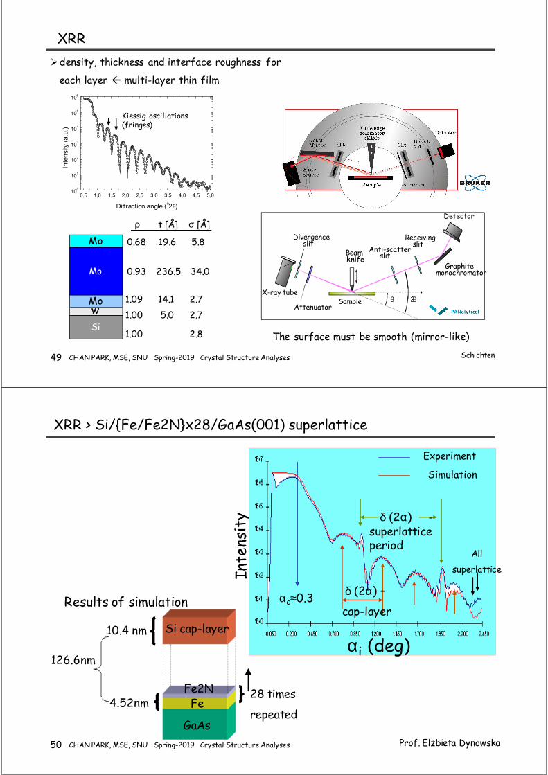
49 CHAN PARK, MSE, SNU Spring-2019 Crystal Structure Analyses
XRR
density, thickness and interface roughness for
each layer multi-layer thin film
The surface must be smooth (mirror-like)
0,5 1,0 1,5 2,0 2,5 3,0 3,5 4,0 4,5 5,010
0
101
102
103
104
105
106
Inte
nsity
(a
.u.)
Diffraction angle (o2θ)
Kiessig oscillations (fringes)
Schichten
Si
Mo
Mo
Mo
ρ t [Å] σ [Å]
0.68 19.6 5.8
0.93 236.5 34.0
W
1.09 14.1 2.7
1.00 5.0 2.7
1.00 2.8
θ 2θX-ray tube
Divergence slit
AttenuatorSample
Detector
Graphite monochromator
Anti-scatter slitBeam
knife
Receiving slit
50 CHAN PARK, MSE, SNU Spring-2019 Crystal Structure Analyses
XRR > Si/{Fe/Fe2N}x28/GaAs(001) superlattice
28 times
repeatedGaAs
FeFe2N
Si cap-layer
Results of simulation
10.4 nm
4.52nm
126.6nmαi (deg)
αc≈0.3
δ (2α) -superlattice period
δ (2α) –
cap-layer
Experiment
Simulation
All
superlattice
Prof. Elżbieta Dynowska
51 CHAN PARK, MSE, SNU Spring-2019 Crystal Structure Analyses
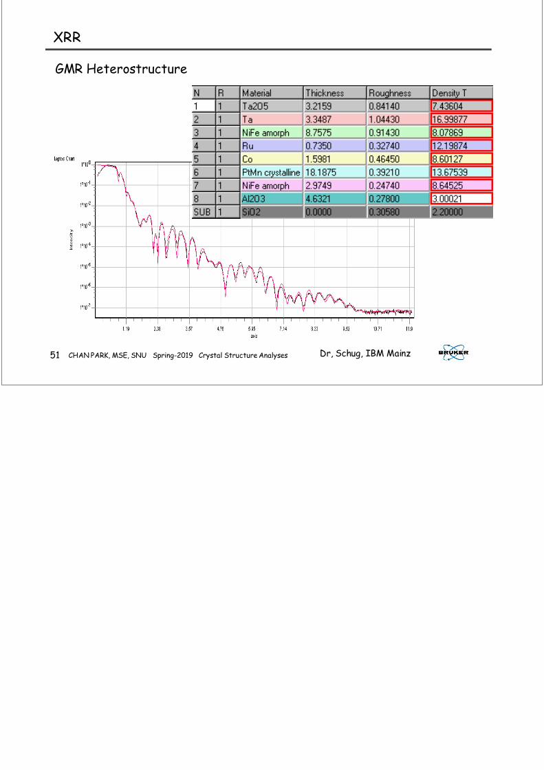
XRR
GMR Heterostructure
Dr, Schug, IBM Mainz