Embed Size (px)
Citation preview
Applications of XAFS to
materials and nano – science
Federico Boscherini
Department of Physics and Astronomy
University of Bologna, Italy
www.unibo.it/faculty/federico.boscherini
Tutorial on XAFS, IUCr Congress, Montreal, August 5th, 2014

Plan• Examples of applications, using both
– results which have “stood the test of time”
– recent results
Today’s topics
• Dopants, defects
• Alloys
• Phase transitions
• Thin films, interfaces
• Nanostructures
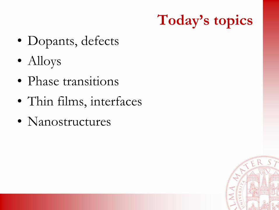
XAFS and dopants/dilute elements
• Only the structure around the photo-excited
atom is probed
• Fluorescence detection greatly enhances
sensitivity
• Present sensitivity limit (depends on sample)
– dopants in the bulk
• EXAFS 1018 at/cm3
• XANES 1017 at/cm3
– thin films (single layer) 1014 at/cm2
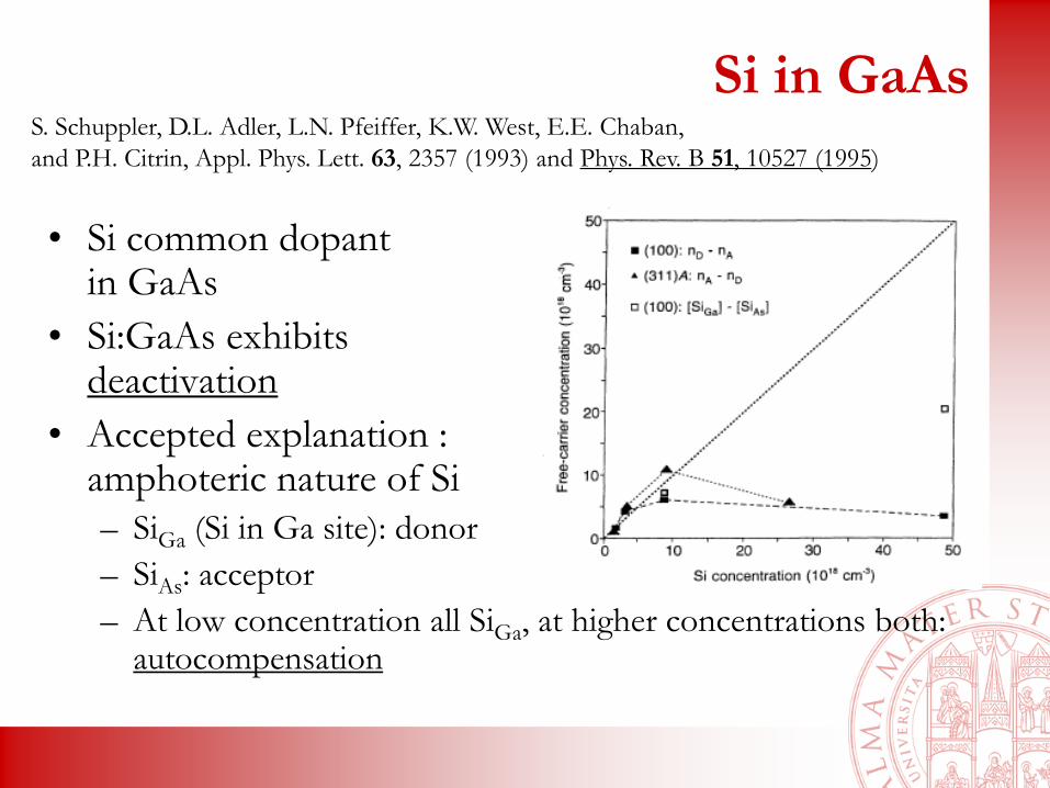
Si in GaAs
• Si common dopant in GaAs
• Si:GaAs exhibits deactivation
• Accepted explanation : amphoteric nature of Si
– SiGa (Si in Ga site): donor
– SiAs: acceptor
– At low concentration all SiGa, at higher concentrations both: autocompensation
S. Schuppler, D.L. Adler, L.N. Pfeiffer, K.W. West, E.E. Chaban,
and P.H. Citrin, Appl. Phys. Lett. 63, 2357 (1993) and Phys. Rev. B 51, 10527 (1995)
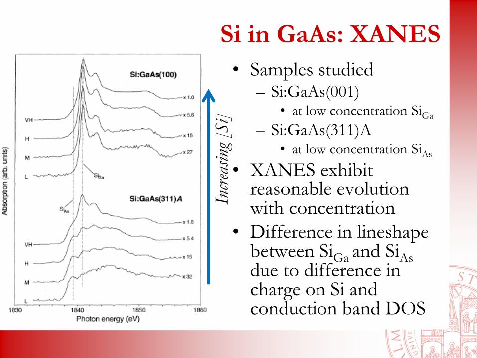
Si in GaAs: XANES
• Samples studied– Si:GaAs(001)
• at low concentration SiGa
– Si:GaAs(311)A• at low concentration SiAs
• XANES exhibit reasonable evolution with concentration
• Difference in lineshape between SiGa and SiAs due to difference in charge on Si and conduction band DOS
Incr
easi
ng [
Si]
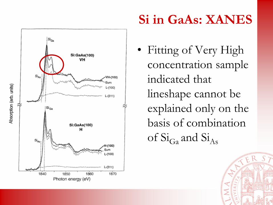
Si in GaAs: XANES
• Fitting of Very High
concentration sample
indicated that
lineshape cannot be
explained only on the
basis of combination
of SiGa and SiAs

Si in GaAs : EXAFS
• Compare EXAFS spectra with those of SixGe1-x
random alloys
• Ge has similar scattering amplitude to Ga and As
• VH sample spectrum very similar to Si0.2Ge0.8
– 20% of Si is bonded to Si
• Conclusion: deactivation due also to presence ofSi dimers and clusters

Fe in GaN•A. Bonanni, A. Navarro-Quezada, Tian Li, M. Wegscheider, Z. Matěj, V. Holý, R. T. Lechner, G. Bauer, M. Rovezzi,
F. D’Acapito, M. Kiecana, M. Sawicki, and T. Dietl, Phys. Rev. Lett. 101, 135502 (2008)
• M. Rovezzi, F. D’Acapito, A. Navarro-Quezada, B. Faina, T. Li, A. Bonanni, F. Filippone, A. Amore Bonapasta,
and T. Dietl, Phys. Rev. B 79, 195209 (2009)
•A. Navarro-Quezada, W. Stefanowicz, Tian Li, B. Faina, M. Rovezzi, R. T. Lechner, T. Devillers, F. D’Acapito,
G. Bauer, M. Kiecana, M. Sawicki, T. Dietl, and A. Bonanni Phys. Rev. 81, 205206 (2010)
• Candidate material for spintronic applications
• Grown by Metal Organic Vapor Phase Epitaxy
• Fe concentrations
4 1019 cm-3 - 4 1020 cm-3
• Aims:
– Determine the site of Fe in GaN
– Determine the effect of Si co-dopant
– Correlate with magnetic properties
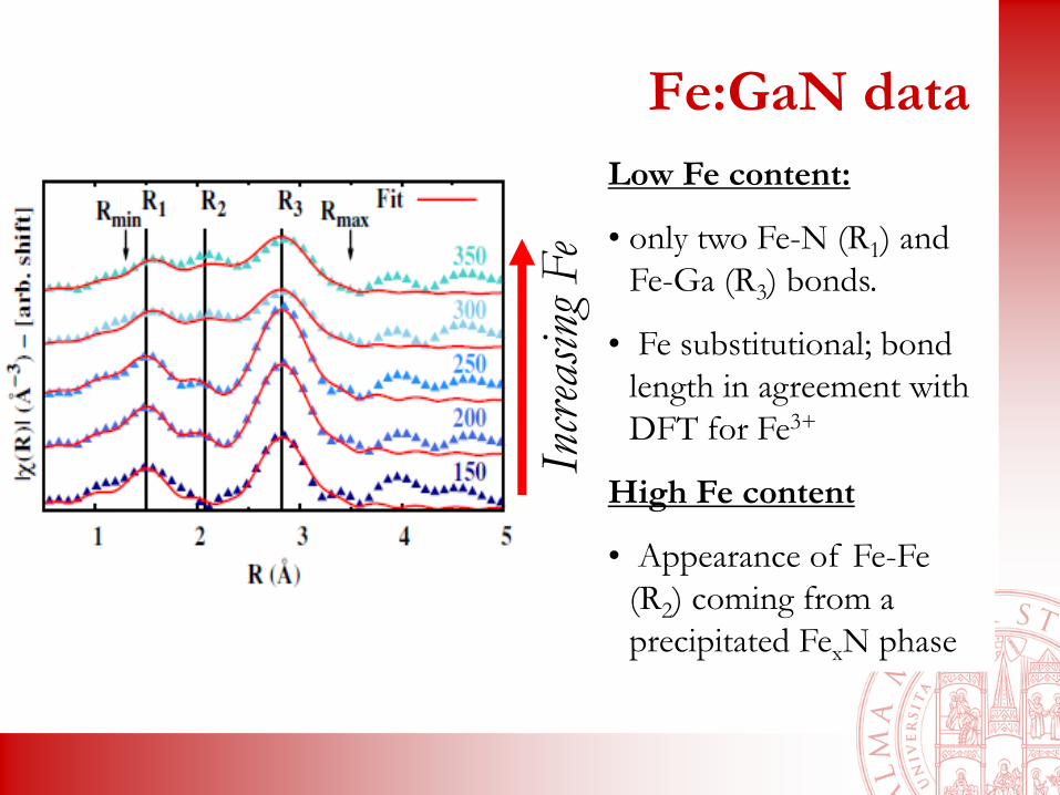
Fe:GaN data
Low Fe content:
• only two Fe-N (R1) and
Fe-Ga (R3) bonds.
• Fe substitutional; bond
length in agreement with
DFT for Fe3+
High Fe content
• Appearance of Fe-Fe
(R2) coming from a
precipitated FexN phase
Incr
easi
ng F
e
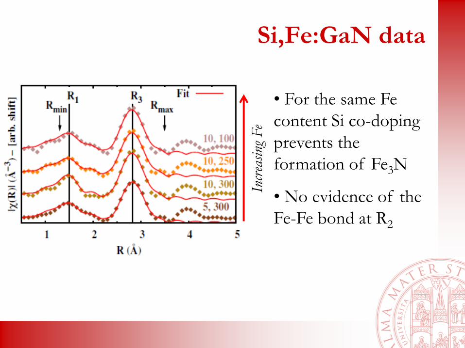
Si,Fe:GaN data
• For the same Fe
content Si co-doping
prevents the
formation of Fe3N
• No evidence of the
Fe-Fe bond at R2
Incr
easi
ng F
e
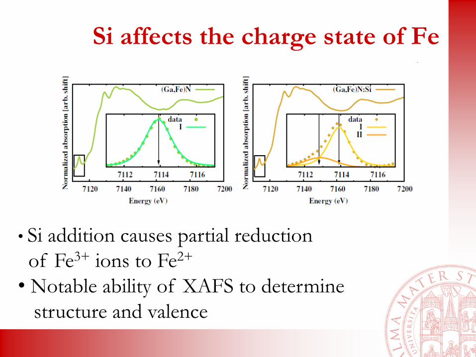
Si affects the charge state of Fe
• Si addition causes partial reduction
of Fe3+ ions to Fe2+
• Notable ability of XAFS to determine
structure and valence
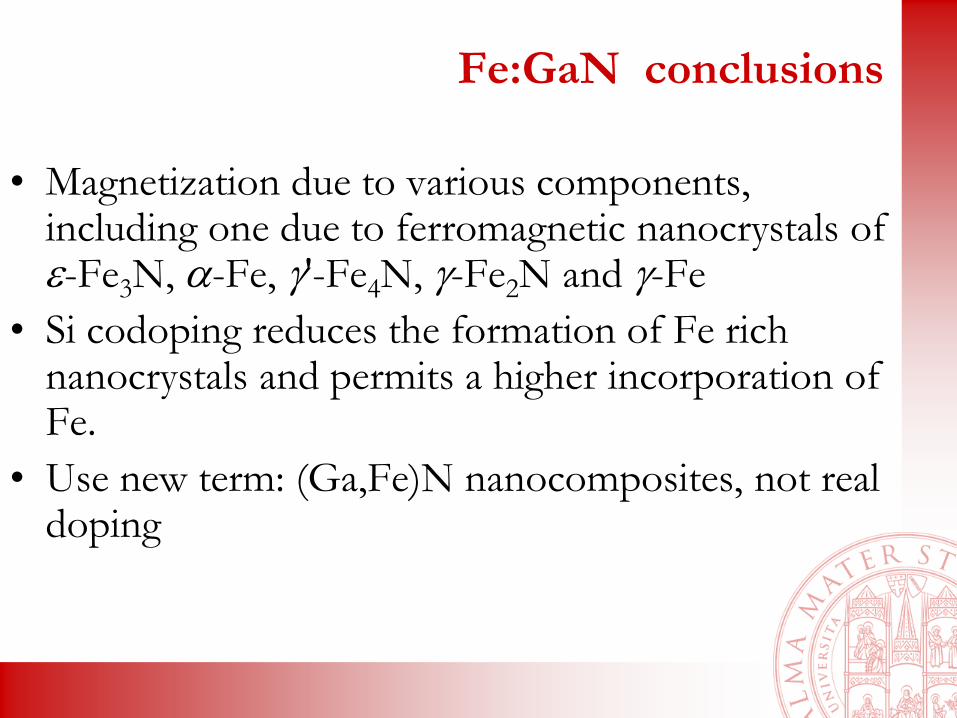
Fe:GaN conclusions
• Magnetization due to various components, including one due to ferromagnetic nanocrystals of e-Fe3N, a-Fe, g'-Fe4N, g-Fe2N and g-Fe
• Si codoping reduces the formation of Fe rich nanocrystals and permits a higher incorporation of Fe.
• Use new term: (Ga,Fe)N nanocomposites, not real doping

Low Z dopants and XAS• C, N & O often used as dopants
• Experimentally difficult: low fluorescence yield, soft X-rays, UHV
ALOISA beamline @ ELETTRA10
-4
10-3
10-2
10-1
100
5 10 15 20 25 30
Flu
ore
scen
ceY
ield
Z
K edges LIII
edges
K edge yield
LIII
edge yield

Dilute nitrides: GaAs1-yNy, InxGa1-xAs1-yNy
0.0 0.5 1.0
3.25 eV
Eg (eV)
GaAs
GaN
y
1.42 eV
• Anomalous non-linear optical
and electronic proprieties of
III-V nitrides
• Red shift of the band gap by
adding few % of nitrogen (
0.05-0.1 eV per N atomic
percent in InGaAsN )
• Huge and composition
dependent optical bowing
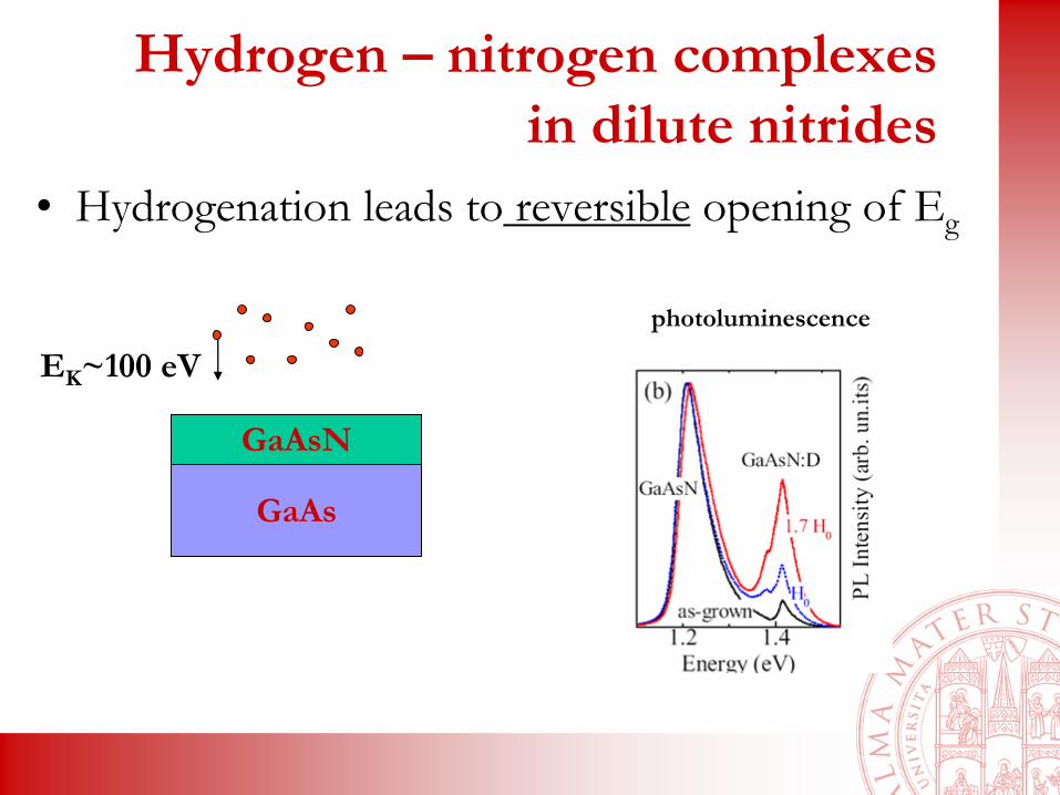
Hydrogen – nitrogen complexes
in dilute nitrides
• Hydrogenation leads to reversible opening of Eg
photoluminescence
GaAs
GaAsN
EK~100 eV

Hydrogen – nitrogen complexes in
dilute nitrides
• Which is the hydrogen
–nitrogen complex
responsible for these
changes?
Some candidate
low energy structures
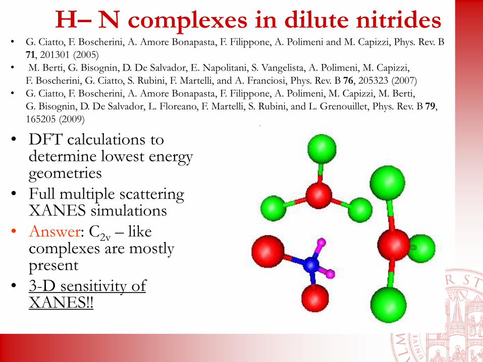
H– N complexes in dilute nitrides
• DFT calculations to determine lowest energygeometries
• Full multiple scatteringXANES simulations
• Answer: C2v – likecomplexes are mostlypresent
• 3-D sensitivity of XANES!! 390 400 410 420 430
Ab
sorp
tio
n c
ross
-sec
tio
n
Energy (eV)
N-HBC
N-H3
C2v
As grown
Hydrogenated
• G. Ciatto, F. Boscherini, A. Amore Bonapasta, F. Filippone, A. Polimeni and M. Capizzi, Phys. Rev. B
71, 201301 (2005)
• M. Berti, G. Bisognin, D. De Salvador, E. Napolitani, S. Vangelista, A. Polimeni, M. Capizzi,
F. Boscherini, G. Ciatto, S. Rubini, F. Martelli, and A. Franciosi, Phys. Rev. B 76, 205323 (2007)
• G. Ciatto, F. Boscherini, A. Amore Bonapasta, F. Filippone, A. Polimeni, M. Capizzi, M. Berti,
G. Bisognin, D. De Salvador, L. Floreano, F. Martelli, S. Rubini, and L. Grenouillet, Phys. Rev. B 79,
165205 (2009)
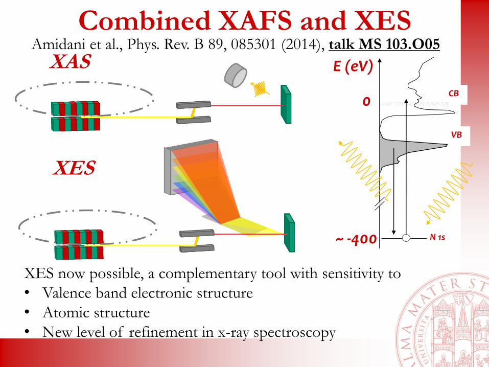
XAS
XES
VB
CB
N 1s~ -400
0
E (eV)
XES now possible, a complementary tool with sensitivity to
• Valence band electronic structure
• Atomic structure
• New level of refinement in x-ray spectroscopy
Combined XAFS and XESAmidani et al., Phys. Rev. B 89, 085301 (2014), talk MS 103.O05
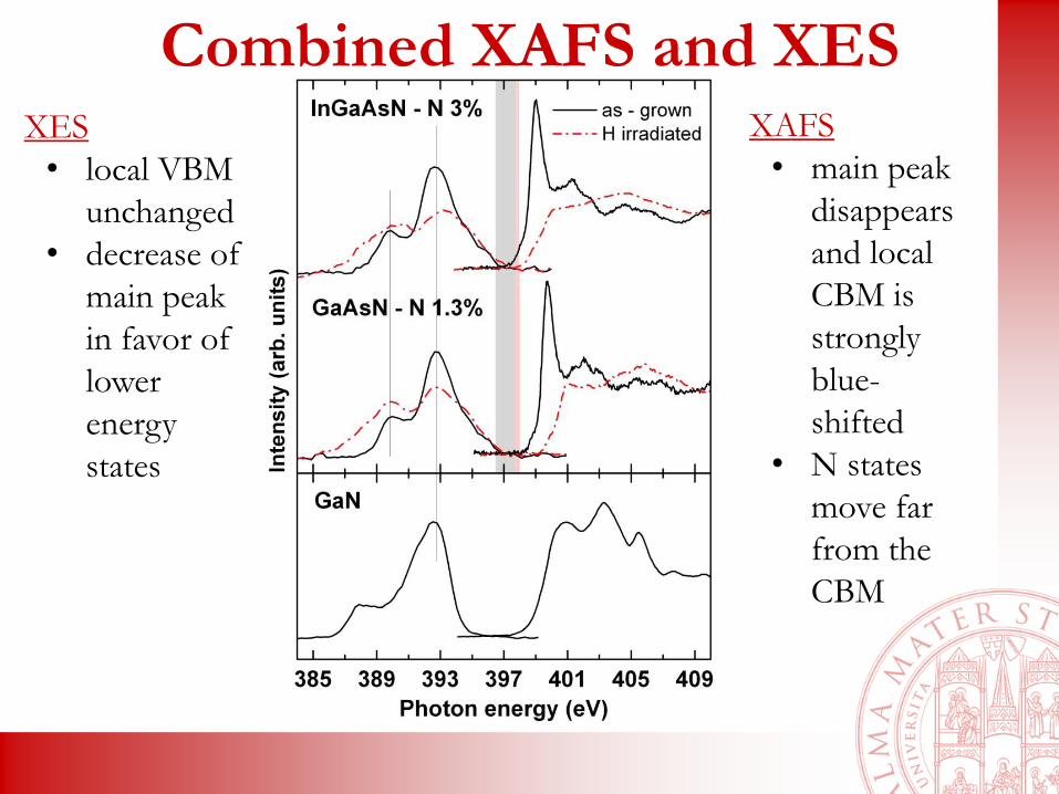
XAFS
• main peak
disappears
and local
CBM is
strongly
blue-
shifted
• N states
move far
from the
CBM
XES
• local VBM
unchanged
• decrease of
main peak
in favor of
lower
energy
states
Combined XAFS and XES
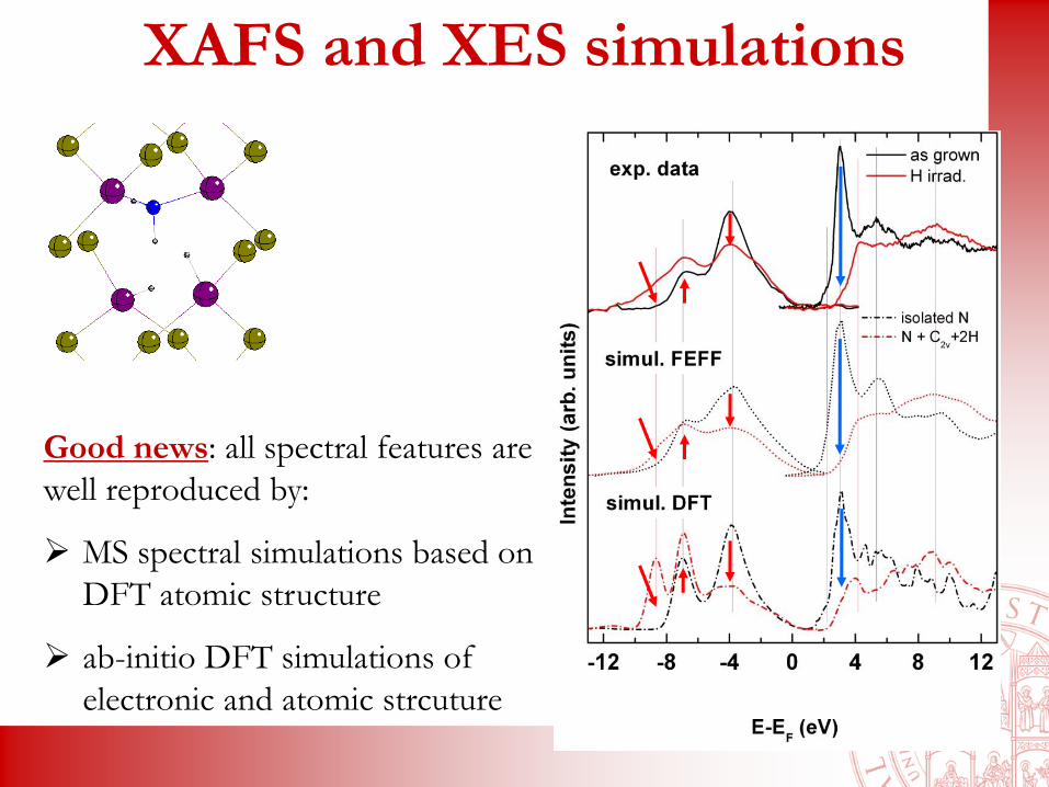
XAFS and XES simulations
Good news: all spectral features are
well reproduced by:
MS spectral simulations based on
DFT atomic structure
ab-initio DFT simulations of
electronic and atomic strcuture
XAFS and alloys
• High resolution in probing the local
coordination in first few coordination shells
• Study, as a function of composition
– Deviation of local structure from average
structure
– Atomic ordering

Semiconductor alloys
• For example: InxGa1-xAs
• Alloying leads to changes in
– band-gap
– lattice parameter
Lattice parameter (Å)
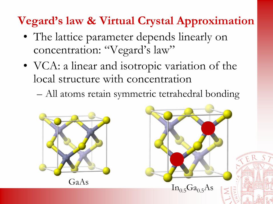
Vegard’s law & Virtual Crystal Approximation
• The lattice parameter depends linearly on concentration: “Vegard’s law”
• VCA: a linear and isotropic variation of the local structure with concentration
– All atoms retain symmetric tetrahedral bonding
GaAsIn0.5Ga0.5As

Bond lengths in InxGa1-xAs
• The high resolution of EXAFS in determining bond lengths (0.01 Å) has shown that they stay close to sum of covalent radii
• Violation of the VCA• First evidence of strong local
structural distortions• Mikkelsen Jr. and Boyce,
Phys. Rev. Lett. 49, 1412 (1982)

XAFS and phase transitions
• Measure local structure through the phase
transition
• XAFS has highlighted the difference between
the real local structure and the average
structure
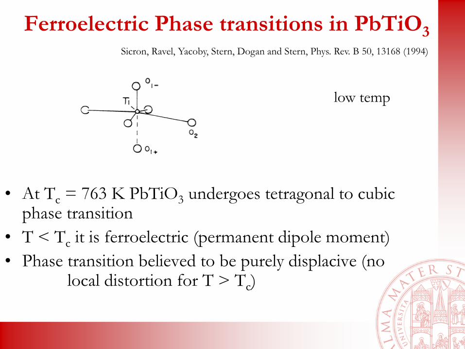
Ferroelectric Phase transitions in PbTiO3
• At Tc = 763 K PbTiO3 undergoes tetragonal to cubic phase transition
• T < Tc it is ferroelectric (permanent dipole moment)
• Phase transition believed to be purely displacive (nolocal distortion for T > Tc)
low temp
Sicron, Ravel, Yacoby, Stern, Dogan and Stern, Phys. Rev. B 50, 13168 (1994)
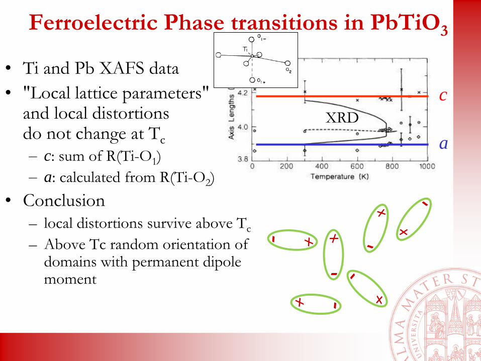
Ferroelectric Phase transitions in PbTiO3
• Ti and Pb XAFS data
• "Local lattice parameters"and local distortionsdo not change at Tc
– c: sum of R(Ti-O1)
– a: calculated from R(Ti-O2)
• Conclusion
– local distortions survive above Tc
– Above Tc random orientation of domains with permanent dipolemoment
c
a
XRD
+
-
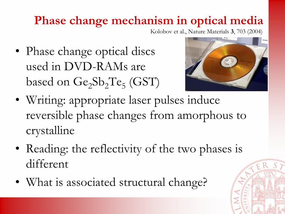
Phase change mechanism in optical media
• Phase change optical discs
used in DVD-RAMs are
based on Ge2Sb2Te5 (GST)
• Writing: appropriate laser pulses induce
reversible phase changes from amorphous to
crystalline
• Reading: the reflectivity of the two phases is
different
• What is associated structural change?
Kolobov et al., Nature Materials 3, 703 (2004)
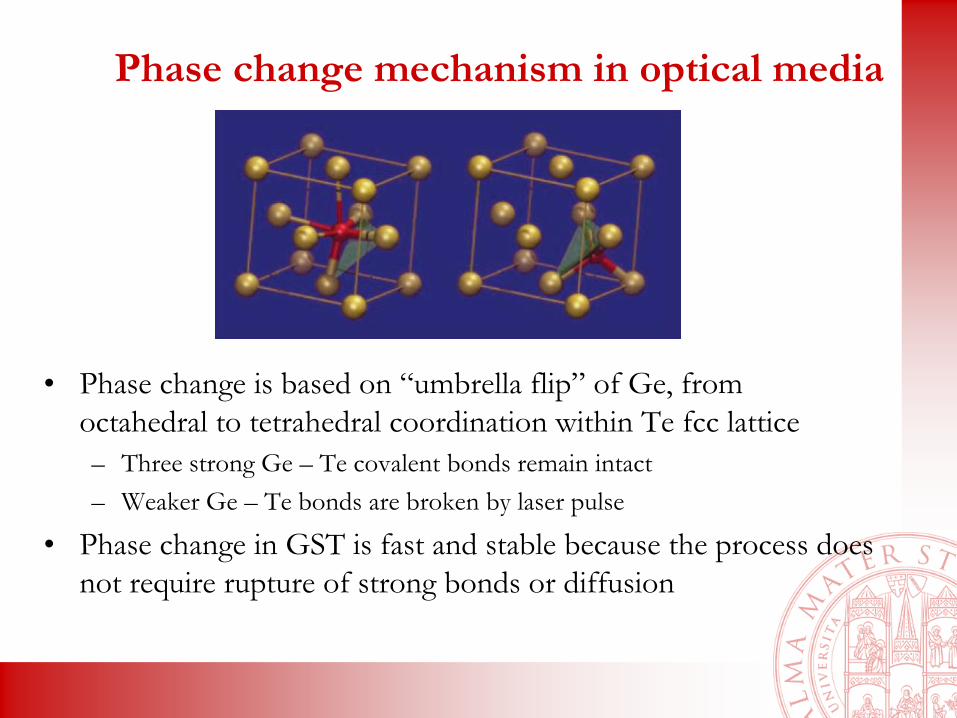
Phase change mechanism in optical media
• Phase change is based on “umbrella flip” of Ge, from
octahedral to tetrahedral coordination within Te fcc lattice
– Three strong Ge – Te covalent bonds remain intact
– Weaker Ge – Te bonds are broken by laser pulse
• Phase change in GST is fast and stable because the process does
not require rupture of strong bonds or diffusion

Time resolved XAFS of phase change
• Sub nanosecond time resolved XAFS with mm spot size at SPring-8
• The intensity of the “white line” is different for crystalline, amorphous and liquid phases
Fons et al., Phys. Rev. B 82, 041203 (2010)
As-deposited
amorphous
Crystallized band
Amorphous
marks
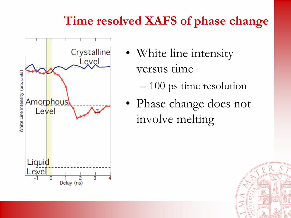
Time resolved XAFS of phase change
• White line intensity
versus time
– 100 ps time resolution
• Phase change does not
involve melting
XAFS and thin films / interfaces
• With specific detection schemes sensitivity to
very thin films achievable
– Grazing incidence
– Electron / fluo detection
• Exploit linear polarization of SR to obtain
information on
– Orientation
– Lattice symmetry
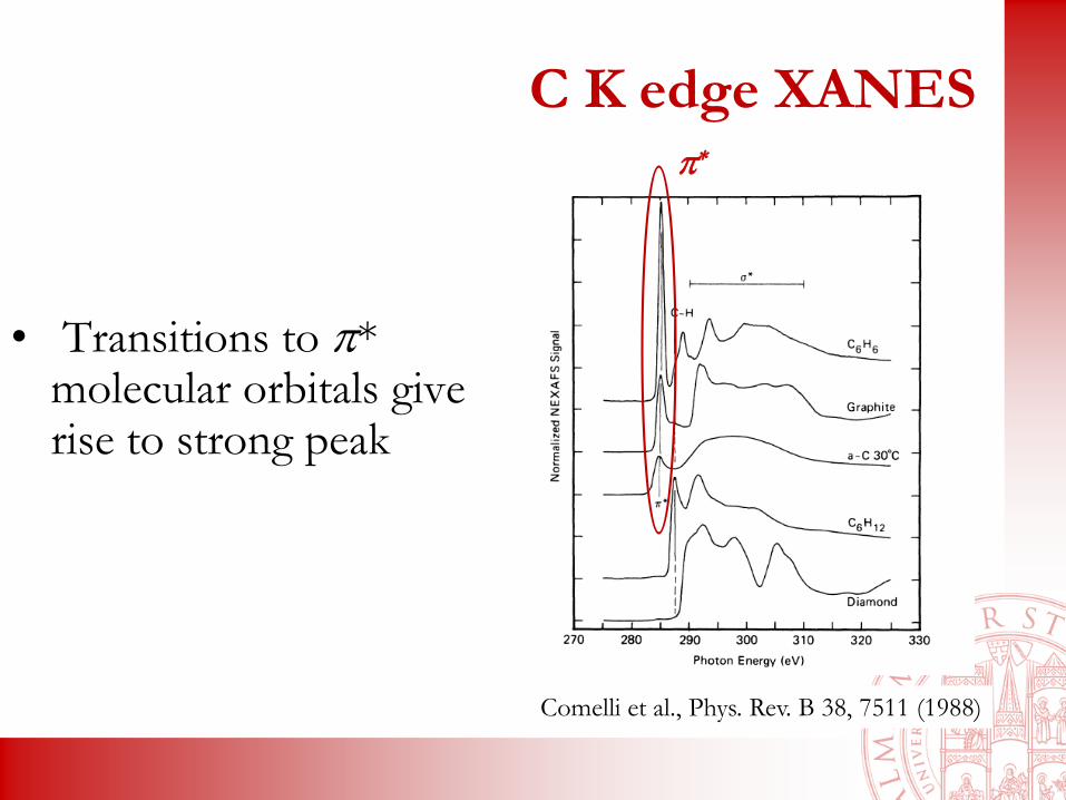
C K edge XANES
• Transitions to p* molecular orbitals give rise to strong peak
Comelli et al., Phys. Rev. B 38, 7511 (1988)
p*
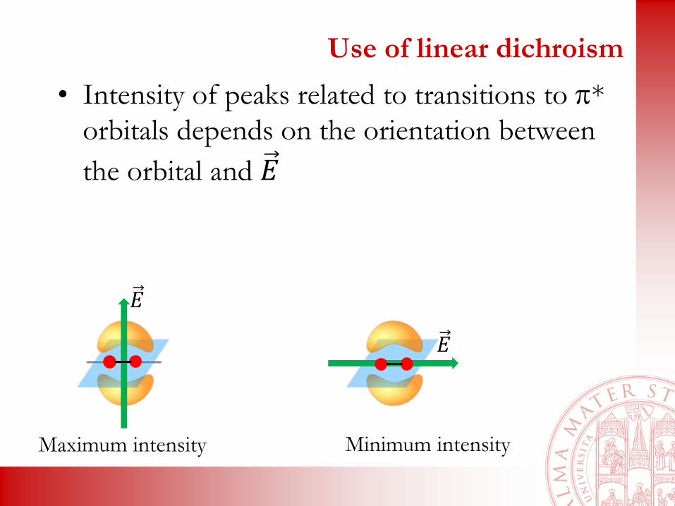
Use of linear dichroism
• Intensity of peaks related to transitions to p*
orbitals depends on the orientation between
the orbital and 𝐸
Maximum intensity Minimum intensity
𝐸
𝐸
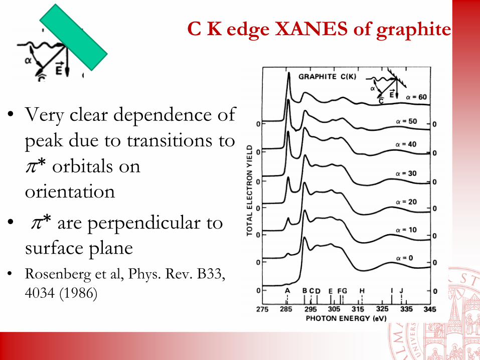
C K edge XANES of graphite
• Very clear dependence of
peak due to transitions to
p* orbitals on
orientation
• p* are perpendicular to
surface plane
• Rosenberg et al, Phys. Rev. B33,
4034 (1986)
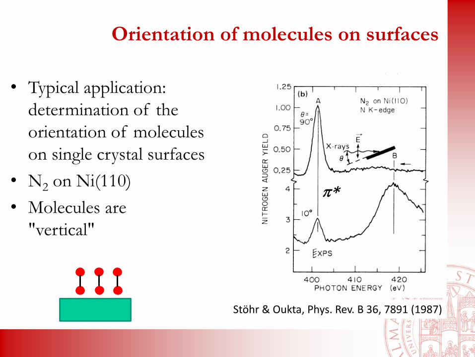
• Typical application:
determination of the
orientation of molecules
on single crystal surfaces
• N2 on Ni(110)
• Molecules are
"vertical"
Orientation of molecules on surfaces
Stöhr & Oukta, Phys. Rev. B 36, 7891 (1987)
p*

XAFS and nanostructures
• XAFS is a local, short range, effect
– Origin: core hole lifetime (thole = 10-16 – 10-15 s) and electron mean free path (5 – 10 Å).
• Same formalism applies to molecule, cluster or crystalline solid
– insenstive to variations of morphology
– sensitive to low thicknesses, high dilutions
• Excellent probe of variations in local environment due to
– Size effects
– Change 3D / 2D / 1D
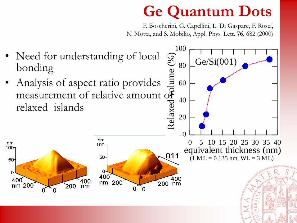
Ge Quantum Dots
• Need for understanding of localbonding
• Analysis of aspect ratio providesmeasurement of relative amount of relaxed islands
F. Boscherini, G. Capellini, L. Di Gaspare, F. Rosei,
N. Motta, and S. Mobilio, Appl. Phys. Lett. 76, 682 (2000)
0
20
40
60
80
100
0 5 10 15 20 25 30 35 40
Rel
axed
vo
lum
e (%
)
equivalent thickness (nm)
Ge/Si(001)
(1 ML = 0.135 nm, WL = 3 ML)

Quantum Dots: Ge edge XAFS
0 2 4 6
Ge in Si
Ge bulk
dots
interatomic distance (Å)
Ge
Fou T
ransf
0
1
2
3
4
2 4 6 8 10 12 14 16
k (Å-1
)
k
(k)
(Å-1
)
Ge:Si
(111)
1 nm
(001)
7.8 nm
(001)
38 nm
Ge
•Assuming random alloyaverage composition
is Ge0.70Si0.30
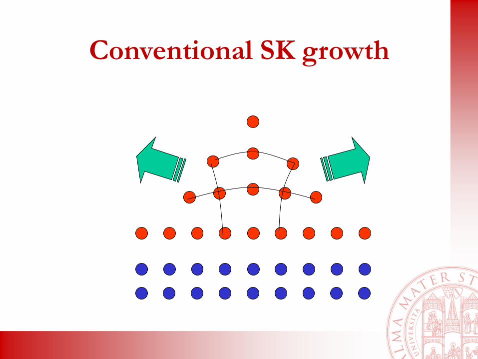
Conventional SK growth
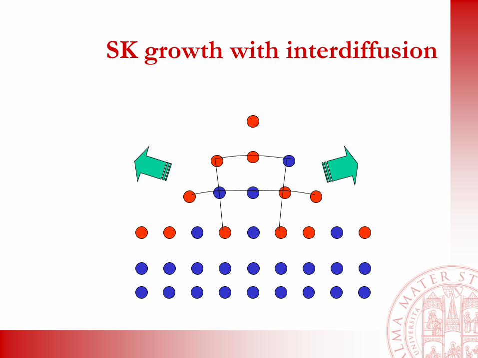
SK growth with interdiffusion
Conclusions
• XAFS has been used to address important
structural issues in materials/nano science
• It has specific advantages, especially– Atomic selectivity
– Sensitivity to high dilutions & surfaces/interfaces
– Equally applicable to ordered or disordered matter
– EXAFS: high resolution for first few coordination shells
– XANES:
• valence/oxidation state
• 3D structural sensitivity
– mm spot size now available and decreasing fast
– Time resolution in the 10 -100 ps range available and with FELs
decreasing to 10 fs
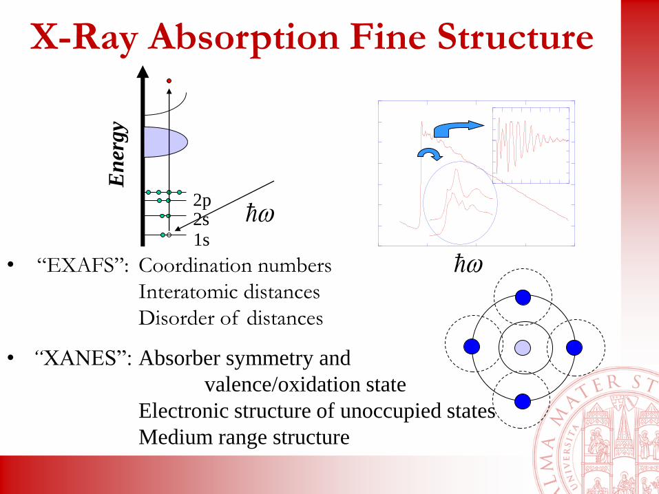
X-Ray Absorption Fine Structure
• “EXAFS”: Coordination numbers
Interatomic distances
Disorder of distances
• “XANES”: Absorber symmetry and
valence/oxidation state
Electronic structure of unoccupied states
Medium range structure
Ener
gy
1s2s2p

EXAFS• Extended X-ray Absorption Fine Structure
• When applicable, fit with the “standard” EXAFS
equation
Debye Waller factor
- thermal vibration
- static disorder
Coordination
number
Interatomic
distance
222
1
2
0 ]22[)()( jk
jjj
shellsj
j ekrSinkANSk
Measure:
From ab-initio calculations or from reference compounds
BEmk
2

XANES• X-ray Absorption Near Edge Structure
(also NEXAFS)
• “Molecular orbital” approach: 1 electron approximation,
constant matrix element: probe site and symmetry projected
density of states of final electronic states
• “Multiple scattering” approach: structural interpretation through
simulation
)(ˆ422
fEfri eap
light) pol. (lin.
0,1 m
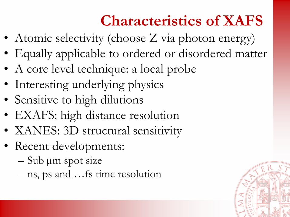
Characteristics of XAFS• Atomic selectivity (choose Z via photon energy)
• Equally applicable to ordered or disordered matter
• A core level technique: a local probe
• Interesting underlying physics
• Sensitive to high dilutions
• EXAFS: high distance resolution
• XANES: 3D structural sensitivity
• Recent developments:– Sub mm spot size
– ns, ps and …fs time resolution

Role of XAFS in Materials Science
Nakamura et al., Jpn. J. Appl. Phys. 35, L217, 1996
Growth
MBE@TASC
Structure
Physical Properties
XAFS
Objective: an understanding of physical properties of novel materials based on knowledge of their local structure