Embed Size (px)
Citation preview
1/25
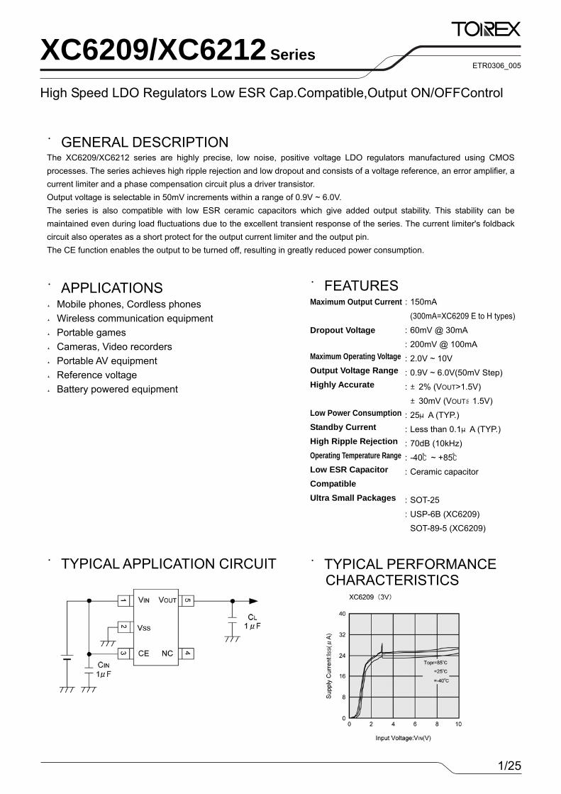
High Speed LDO Regulators Low ESR Cap.Compatible,Output ON/OFFControl
XC6209/XC6212 Series
■GENERAL DESCRIPTION The XC6209/XC6212 series are highly precise, low noise, positive voltage LDO regulators manufactured using CMOS processes. The series achieves high ripple rejection and low dropout and consists of a voltage reference, an error amplifier, a current limiter and a phase compensation circuit plus a driver transistor. Output voltage is selectable in 50mV increments within a range of 0.9V ~ 6.0V. The series is also compatible with low ESR ceramic capacitors which give added output stability. This stability can be maintained even during load fluctuations due to the excellent transient response of the series. The current limiter's foldback circuit also operates as a short protect for the output current limiter and the output pin. The CE function enables the output to be turned off, resulting in greatly reduced power consumption.
■APPLICATIONS ●Mobile phones, Cordless phones ●Wireless communication equipment ●Portable games ●Cameras, Video recorders ●Portable AV equipment ●Reference voltage ●Battery powered equipment
■TYPICAL APPLICATION CIRCUIT
■FEATURES Maximum Output Current Dropout Voltage Maximum Operating Voltage Output Voltage Range Highly Accurate Low Power Consumption Standby Current High Ripple Rejection Operating Temperature Range Low ESR Capacitor Compatible Ultra Small Packages
■TYPICAL PERFORMANCE CHARACTERISTICS
: 150mA
(300mA=XC6209 E to H types)
: 60mV @ 30mA
: 200mV @ 100mA
: 2.0V ~ 10V
: 0.9V ~ 6.0V(50mV Step)
: ±2% (VOUT>1.5V)
±30mV (VOUT≦1.5V)
: 25μA (TYP.)
: Less than 0.1μA (TYP.)
: 70dB (10kHz)
: -40℃~ +85℃
: Ceramic capacitor
: SOT-25
: USP-6B (XC6209) SOT-89-5 (XC6209)
ETR0306_005
2/25
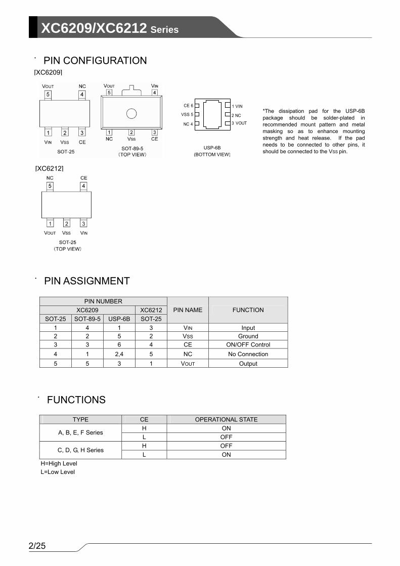
XC6209/XC6212 Series
TYPE CE OPERATIONAL STATE
H ON A, B, E, F Series
L OFF H OFF
C, D, G, H Series L ON
H=High Level L=Low Level
■PIN CONFIGURATION [XC6209]
[XC6212]
*The dissipation pad for the USP-6B package should be solder-plated in recommended mount pattern and metal masking so as to enhance mounting strength and heat release. If the pad needs to be connected to other pins, it should be connected to the VSS pin.
VSS 5
NC 4
CE 6 1 VIN
2 NC
3 VOUT
USP-6B (BOTTOM VIEW)
PIN NUMBER XC6209 XC6212
SOT-25 SOT-89-5 USP-6B SOT-25 PIN NAME FUNCTION
1 4 1 3 VIN Input 2 2 5 2 VSS Ground 3 3 6 4 CE ON/OFF Control 4 1 2,4 5 NC No Connection 5 5 3 1 VOUT Output
■PIN ASSIGNMENT
■FUNCTIONS
3/25
XC6209/XC6212Series
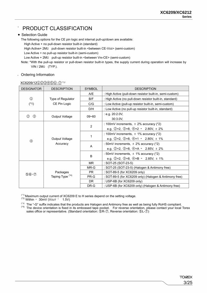
DESIGNATOR DESCRIPTION SYMBOL DESCRIPTION A/E : High Active (pull-down resistor built-in, semi-custom) B/F : High Active (no pull-down resistor built-in, standard) C/G : Low Active (pull-up resistor built-in, semi-custom)
① (*1)
Type of Regulator CE Pin Logic
D/H : Low Active (no pull-up resistor built-in, standard)
② ③ Output Voltage 09~60 : e.g. 20:2.0V, 30:3.0V,
2 : 100mV increments, ±2% accuracy (*2)
e.g. ②=2, ③=8, ④=2 → 2.80V, ±2%
1 : 100mV increments, ±1% accuracy (*2)
e.g. ②=2, ③=8, ④=1 → 2.80V, ±1%
A : 50mV increments, ±2% accuracy (*2)
e.g. ②=2, ③=8, ④=A → 2.85V, ±2%
④ Output Voltage
Accuracy
B : 50mV increments, ±1% accuracy (*2)
e.g. ②=2, ③=8, ④=B → 2.85V, ±1% MR : SOT-25 (SOT-23-5)
MR-G : SOT-25 (SOT-23-5) (Halogen & Antimony free) PR : SOT-89-5 (for XC6209 only)
PR-G : SOT-89-5 (for XC6209 only) (Halogen & Antimony free) DR : USP-6B (for XC6209 only)
⑤⑥-⑦ Packages
Taping Type (*4)
DR-G : USP-6B (for XC6209 only) (Halogen & Antimony free)
■PRODUCT CLASSIFICATION●Selection Guide
The following options for the CE pin logic and internal pull-up/down are available: High Active + no pull-down resistor built-in (standard) High Active+ 2MΩ pull-down resistor built-in <between CE-VSS> (semi-custom) Low Active + no pull-up resistor built-in (semi-custom) Low Active + 2MΩ pull-up resistor built-in <between VIN-CE> (semi-custom)
Note: *With the pull-up resistor or pull-down resistor built-in types, the supply current during operation will increase by VIN / 2MΩ (TYP.).
●Ordering Information
(*1) Maximum output current of XC6209 E to H series depend on the setting voltage.(*2) Within ±30mV (VOUT ≦ 1.5V)
XC6209/12①②③④⑤⑥-⑦(*3)
(*3) The “-G” suffix indicates that the products are Halogen and Antimony free as well as being fully RoHS compliant.(*4) The device orientation is fixed in its embossed tape pocket. For reverse orientation, please contact your local Torex
sales office or representative. (Standard orientation: ⑤R-⑦, Reverse orientation: ⑤L-⑦)
4/25
XC6209/XC6212 Series
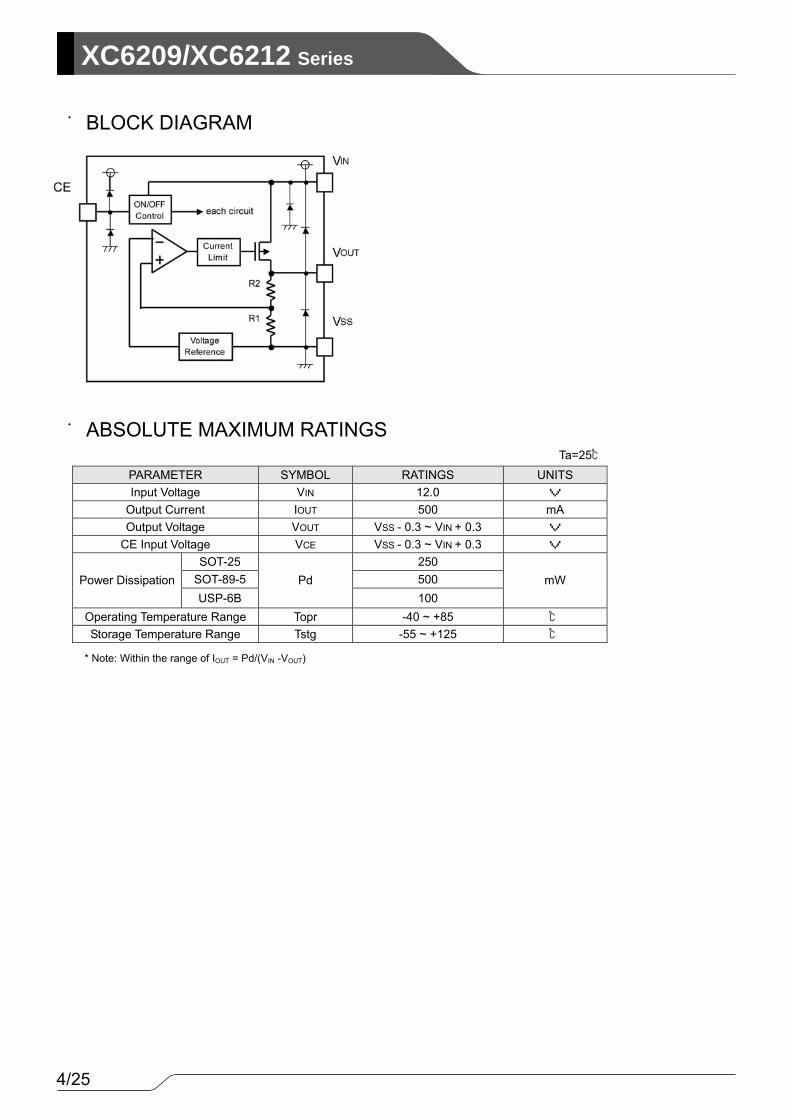
PARAMETER SYMBOL RATINGS UNITS Input Voltage VIN 12.0 V
Output Current IOUT 500 mA Output Voltage VOUT VSS - 0.3 ~ VIN + 0.3 V
CE Input Voltage VCE VSS - 0.3 ~ VIN + 0.3 V SOT-25 250
SOT-89-5 500 Power Dissipation USP-6B
Pd 100
mW
Operating Temperature Range Topr -40 ~ +85 ℃ Storage Temperature Range Tstg -55 ~ +125 ℃
■BLOCK DIAGRAM
■ABSOLUTE MAXIMUM RATINGSTa=25℃
* Note: Within the range of IOUT = Pd/(VIN -VOUT)
5/25
XC6209/XC6212Series
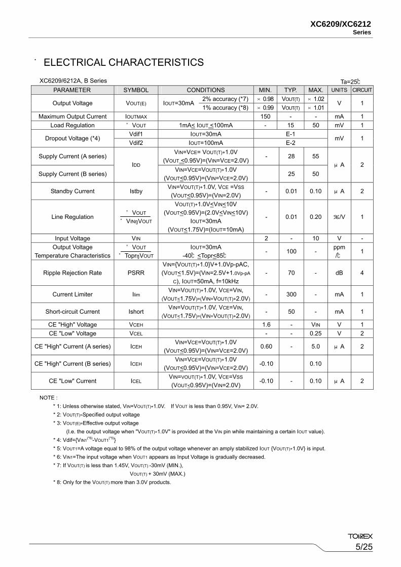
PARAMETER SYMBOL CONDITIONS MIN. TYP. MAX. UNITS CIRCUIT
2% accuracy (*7) ×0.98 VOUT(T) ×1.02 Output Voltage VOUT(E) IOUT=30mA
1% accuracy (*8) ×0.99 VOUT(T) ×1.01 V 1
Maximum Output Current IOUTMAX 150 - - mA 1 Load Regulation △VOUT 1mA< IOUT <100mA - 15 50 mV 1
Vdif1 IOUT=30mA E-1 Dropout Voltage (*4)
Vdif2 IOUT=100mA E-2 mV 1
Supply Current (A series) VIN=VCE= VOUT(T)+1.0V
(VOUT <0.95V)=(VIN=VCE=2.0V)- 28 55
Supply Current (B series) IDD
VIN=VCE=VOUT(T)+1.0V (VOUT<0.95V)=(VIN=VCE=2.0V)
25 50 μA 2
Standby Current Istby VIN=VOUT(T)+1.0V, VCE =VSS (VOUT<0.95V)=(VIN=2.0V)
- 0.01 0.10 μA 2
Line Regulation
△VOUT △VIN・VOUT
VOUT(T)+1.0V<VIN<10V (VOUT<0.95V)=(2.0V<VIN<10V)
IOUT=30mA (VOUT<1.75V)=(IOUT=10mA)
- 0.01 0.20 %/V 1
Input Voltage VIN 2 - 10 V - Output Voltage
Temperature Characteristics △VOUT
△Topr・VOUT IOUT=30mA
-40℃<Topr<85℃ - 100 -
ppm/℃
1
Ripple Rejection Rate PSRR VIN={VOUT(T)+1.0}V+1.0Vp-pAC,(VOUT<1.5V)=(VIN=2.5V+1.0Vp-pA
C), IOUT=50mA, f=10kHz - 70 - dB 4
Current Limiter Ilim VIN=VOUT(T)+1.0V, VCE=VIN,
(VOUT<1.75V)=(VIN=VOUT(T)+2.0V)- 300 - mA 1
Short-circuit Current Ishort VIN=VOUT(T)+1.0V, VCE=VIN,
(VOUT<1.75V)=(VIN=VOUT(T)+2.0V)- 50 - mA 1
CE "High" Voltage VCEH 1.6 - VIN V 1 CE "Low" Voltage VCEL - - 0.25 V 2
CE "High" Current (A series) ICEH VIN=VCE=VOUT(T)+1.0V
(VOUT<0.95V)=(VIN=VCE=2.0V)0.60 - 5.0 μA 2
CE "High" Current (B series) ICEH VIN=VCE=VOUT(T)+1.0V
(VOUT<0.95V)=(VIN=VCE=2.0V)-0.10 0.10
CE "Low" Current ICEL VIN=VOUT(T)+1.0V, VCE=VSS (VOUT<0.95V)=(VIN=2.0V)
-0.10 - 0.10 μA 2
■ELECTRICAL CHARACTERISTICS
NOTE : * 1: Unless otherwise stated, VIN=VOUT(T)+1.0V. If VOUT is less than 0.95V, VIN= 2.0V.
* 2: VOUT(T)=Specified output voltage * 3: VOUT(E)=Effective output voltage (I.e. the output voltage when "VOUT(T)+1.0V" is provided at the VIN pin while maintaining a certain IOUT value). * 4: Vdif={VIN1
(*6)-VOUT1(*5)}
* 5: VOUT1=A voltage equal to 98% of the output voltage whenever an amply stabilized IOUT {VOUT(T)+1.0V} is input. * 6: VIN1=The input voltage when VOUT1 appears as Input Voltage is gradually decreased. * 7: If VOUT(T) is less than 1.45V, VOUT(T) -30mV (MIN.), VOUT(T) + 30mV (MAX.) * 8: Only for the VOUT(T) more than 3.0V products.
Ta=25℃XC6209/6212A, B Series
6/25
XC6209/XC6212 Series
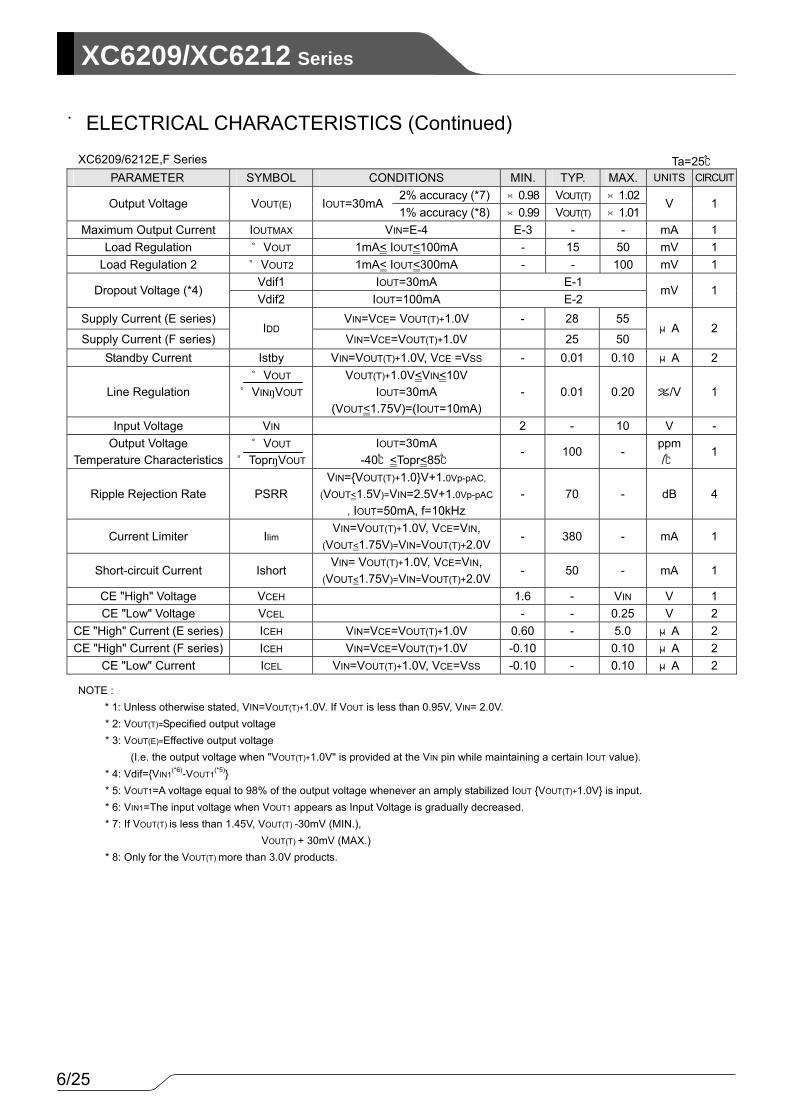
PARAMETER SYMBOL CONDITIONS MIN. TYP. MAX. UNITS CIRCUIT
2% accuracy (*7) ×0.98 VOUT(T) ×1.02 Output Voltage VOUT(E) IOUT=30mA
1% accuracy (*8) ×0.99 VOUT(T) ×1.01 V 1
Maximum Output Current IOUTMAX VIN=E-4 E-3 - - mA 1 Load Regulation △VOUT 1mA< IOUT<100mA - 15 50 mV 1
Load Regulation 2 △VOUT2 1mA< IOUT<300mA - - 100 mV 1 Vdif1 IOUT=30mA E-1
Dropout Voltage (*4) Vdif2 IOUT=100mA E-2
mV 1
Supply Current (E series) VIN=VCE= VOUT(T)+1.0V - 28 55
Supply Current (F series) IDD
VIN=VCE=VOUT(T)+1.0V 25 50 μA 2
Standby Current Istby VIN=VOUT(T)+1.0V, VCE =VSS - 0.01 0.10 μA 2
Line Regulation △VOUT △VIN・VOUT
VOUT(T)+1.0V<VIN<10V IOUT=30mA
(VOUT<1.75V)=(IOUT=10mA) - 0.01 0.20 %/V 1
Input Voltage VIN 2 - 10 V - Output Voltage
Temperature Characteristics △VOUT
△Topr・VOUT IOUT=30mA
-40℃<Topr<85℃ - 100 -
ppm/℃
1
Ripple Rejection Rate PSRR VIN={VOUT(T)+1.0}V+1.0Vp-pAC,
(VOUT<1.5V)=VIN=2.5V+1.0Vp-pAC
, IOUT=50mA, f=10kHz - 70 - dB 4
Current Limiter Ilim VIN=VOUT(T)+1.0V, VCE=VIN,
(VOUT<1.75V)=VIN=VOUT(T)+2.0V- 380 - mA 1
Short-circuit Current Ishort VIN= VOUT(T)+1.0V, VCE=VIN,
(VOUT<1.75V)=VIN=VOUT(T)+2.0V- 50 - mA 1
CE "High" Voltage VCEH 1.6 - VIN V 1 CE "Low" Voltage VCEL - - 0.25 V 2
CE "High" Current (E series) ICEH VIN=VCE=VOUT(T)+1.0V 0.60 - 5.0 μA 2 CE "High" Current (F series) ICEH VIN=VCE=VOUT(T)+1.0V -0.10 0.10 μA 2
CE "Low" Current ICEL VIN=VOUT(T)+1.0V, VCE=VSS -0.10 - 0.10 μA 2
■ELECTRICAL CHARACTERISTICS (Continued)
NOTE : * 1: Unless otherwise stated, VIN=VOUT(T)+1.0V. If VOUT is less than 0.95V, VIN= 2.0V.
* 2: VOUT(T)=Specified output voltage * 3: VOUT(E)=Effective output voltage (I.e. the output voltage when "VOUT(T)+1.0V" is provided at the VIN pin while maintaining a certain IOUT value). * 4: Vdif={VIN1
(*6)-VOUT1(*5)}
* 5: VOUT1=A voltage equal to 98% of the output voltage whenever an amply stabilized IOUT {VOUT(T)+1.0V} is input. * 6: VIN1=The input voltage when VOUT1 appears as Input Voltage is gradually decreased. * 7: If VOUT(T) is less than 1.45V, VOUT(T) -30mV (MIN.), VOUT(T) + 30mV (MAX.) * 8: Only for the VOUT(T) more than 3.0V products.
Ta=25℃XC6209/6212E,F Series
7/25
XC6209/XC6212Series
SYMBOL E-0 E-1 E-2 OUTPUT VOLTAGE (V)
(2%) DROPOUT VOLTAGE 1 (mV)
(IOUT=30mA) DROPOUT VOLTAGE 2 (mV)
(IOUT=100mA)
VOUT Vdif1 Vdif2 VOUT(T) MIN MAX TYP MAX TYP MAX
0.90 0.870 0.930 0.95 0.920 0.980 1100 1110 1150 1200
1.00 0.970 1.030 1.05 1.020 1.080 1000 1010 1050 1100
1.10 1.070 1.130 1.15 1.120 1.180 900 910 950 1000
1.20 1.170 1.230 1.25 1.220 1.280 800 810 850 900
1.30 1.270 1.330 1.35 1.320 1.380 700 710 750 800
1.40 1.370 1.430 1.45 1.420 1.480 600 610 650 700
1.50 1.470 1.530 1.55 1.519 1.581 500 510 550 600
1.60 1.568 1.632 1.65 1.617 1.683 400 410 500 550
1.70 1.666 1.734 1.75 1.715 1.785 300 310 400 450
1.80 1.764 1.836 1.85 1.813 1.887 200 210 300 400
1.90 1.862 1.938 1.95 1.911 1.989 120 150 280 380
2.00 1.960 2.040 2.05 2.009 2.091 350
2.10 2.058 2.142 2.15 2.107 2.193 2.20 2.156 2.244 2.25 2.205 2.295
330
2.30 2.254 2.346 2.35 2.303 2.397 2.40 2.352 2.448 2.45 2.401 2.499
80 120 240
310
2.50 2.450 2.550 2.55 2.499 2.601 2.60 2.548 2.652 2.65 2.597 2.703 2.70 2.646 2.754 2.75 2695 2.805
290
2.80 2.744 2.856 2.85 2.793 2.907 2.90 2.842 2.958 2.95 2.891 3.009
70 100 220
3.00 2.940 3.060 3.05 2.989 3.111
270
3.10 3.038 3.162 3.15 3.087 3.213 3.20 3.136 3.264 3.25 3.185 3.315 3.30 3.234 3.366 3.35 3.283 3.417 3.40 3.332 3.468 3.45 3.381 3.519 3.50 3.430 3.570 3.55 3.479 3.621
60 90 200 250
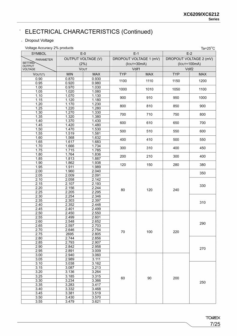
●Dropout Voltage
Voltage Accuracy 2% products
■ELECTRICAL CHARACTERISTICS (Continued)
Ta=25OC
SETTING OUTPUT VOLTAGE
PARAMETER
8/25
XC6209/XC6212 Series
SYMBOL E-0 E-1 E-2 OUTPUT VOLTAGE (V)
(2%) DROPOUT VOLTAGE 1 (mV)
(IOUT=30mA) DROPOUT VOLTAGE 2 (mV)
(IOUT=100mA)
VOUT Vdif1 Vdif2 VOUT(T) MIN MAX TYP MAX TYP MAX
3.60 3.528 3.672 3.65 3.577 3.723 3.70 3.626 3.774 3.75 3.675 3.825 3.80 3.724 3.876 3.85 3.773 3.927 3.90 3.822 3.978 3.95 3.871 4.029
90 200 250
4.00 3.920 4.080 4.05 3.969 4.131 4.10 4.018 4.182 4.15 4.067 4.233 4.20 4.116 4.284 4.25 4.165 4.335 4.30 4.214 4.386 4.35 4.263 4.437 4.40 4.312 4.488 4.45 4.361 4.539 4.50 4.410 4.590 4.55 4.459 4.641 4.60 4.508 4.692 4.65 4.557 4.743 4.70 4.606 4.794 4.75 4.655 4.845 4.80 4.704 4.896 4.85 4.753 4.947 4.90 4.802 4.998 4.95 4.851 5.049
60
80 180 230
5.00 4.900 5.100 5.05 4.949 5.151 5.10 4.998 5.202 5.15 5.047 5.253 5.20 5.096 5.304 5.25 5.145 5.355 5.30 5.194 5.406 5.35 5.243 5.457 5.40 5.292 5.508 5.45 5.341 5.559 5.50 5.390 5.610 5.55 5.439 5.661 5.60 5.488 5.712 5.65 5.537 5.763 5.70 5.586 5.814 5.75 5.635 5.865 5.80 5.684 5.916 5.85 5.733 5.967 5.90 5.782 6.018 5.95 5.831 6.069 6.00 5.880 6.120
50 70 160 210
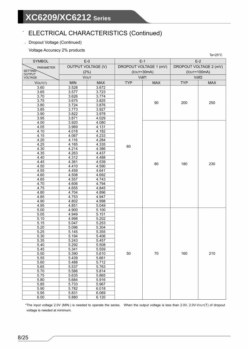
*The input voltage 2.0V (MIN.) is needed to operate the series. When the output voltage is less than 2.0V, 2.0V-VOUT(T) of dropout voltage is needed at minimum.
SETTING OUTPUT VOLTAGE
PARAMETER
●Dropout Voltage (Continued)
Voltage Accuracy 2% products
■ELECTRICAL CHARACTERISTICS (Continued)
Ta=25OC
9/25
XC6209/XC6212Series
SYMBOL E-0 SYMBOL E-0 OUTPUT VOLTAGE (V)
(1%)
OUTPUT VOLTAGE (V) (1%)
VOUT
VOUT VOUT(T) MIN MAX VOUT(T) MIN MAX
3.00 2.970 3.030 4.55 4.505 4.596 3.05 3.020 3.081 4.60 4.554 4.646 3.10 3.069 3.131 4.65 4.604 4.697 3.15 3.119 3.182 4.70 4.653 4.747 3.20 3.168 3.232 4.75 4.703 4.798 3.25 3.218 3.283 4.80 4.752 4.848 3.30 3.267 3.333 4.85 4.802 4.899 3.35 3.317 3.384 4.90 4.851 4.949 3.40 3.366 3.434 4.95 4.901 5.000 3.45 3.416 3.485 5.00 4.950 5.050 3.50 3.465 3.535 5.05 4.000 5.101 3.55 3.515 3.586 5.10 4.049 5.151 3.60 3.564 3.636 5.15 4.099 5.202 3.65 3.614 3.687 5.20 4.148 5.252 3.70 3.663 3.737 5.25 5.198 5.303 3.75 3.713 3.788 5.30 5.247 5.353 3.80 3.762 3.838 5.35 5.297 5.404 3.85 3.812 3.889 5.40 5.346 5.454 3.90 3.861 3.939 5.45 5.396 5.505 3.95 3.911 3.990 5.50 5.445 5.555 4.00 3.960 4.040 5.55 5.495 5.606 4.05 4.010 4.091 5.60 5.544 5.656 4.10 4.059 4.141 5.65 5.594 5.707 4.15 4.109 4.192 5.70 5.643 5.757 4.20 4.158 4.242 5.75 5.963 5.808 4.25 4.208 4.293 5.80 5.742 5.858 4.30 4.257 4.343 5.85 5.792 5.909 4.35 4.307 4.394 5.90 5.841 5.959 4.40 4.356 4.444 5.95 5.891 6.010 4.45 4.405 4.494 6.00 5.940 6.060 4.50 4.455 4.545
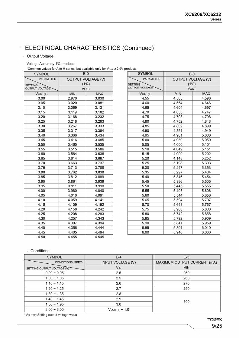
SYMBOL E-4 E-3 . INPUT VOLTAGE (V) MAXIMUM OUTPUT CURRENT (mA)
SETTING OUTPUT VOLTAGE (V) VIN MIN
0.90 ~ 0.95 2.5 260 1.00 ~ 1.05 2.5 260 1.10 ~ 1.15 2.6 270 1.20 ~ 1.25 2.7 290 1.30 ~ 1.35 2.8 1.40 ~ 1.45 2.9 1.50 ~ 1.95 3.0 2.00 ~ 6.00 VOUT(T) + 1.0
300
* VOUT(T): Setting output voltage value
●Output Voltage
Voltage Accuracy 1% products *Common values for A to H series, but available only for VOUT ≥ 2.9V products.
PARAMETER
SETTING OUTPUT VOLTAGE
PARAMETER
SETTING OUTPUT VOLTAGE
●Conditions
CONDITIONS, SPEC
■ELECTRICAL CHARACTERISTICS (Continued)
10/25
XC6209/XC6212 Series
1 Please use this IC within the stated absolute maximum ratings.
The IC is liable to malfunction should the ratings be exceeded. 2 Where wiring impedance is high, operations may become unstable due to noise and/or phase lag depending on
output current. Please strengthen VIN and VSS wiring in particular. 3 Please wire the input capacitor (CIN) and the output capacitor (CL) as close to the IC as possible.
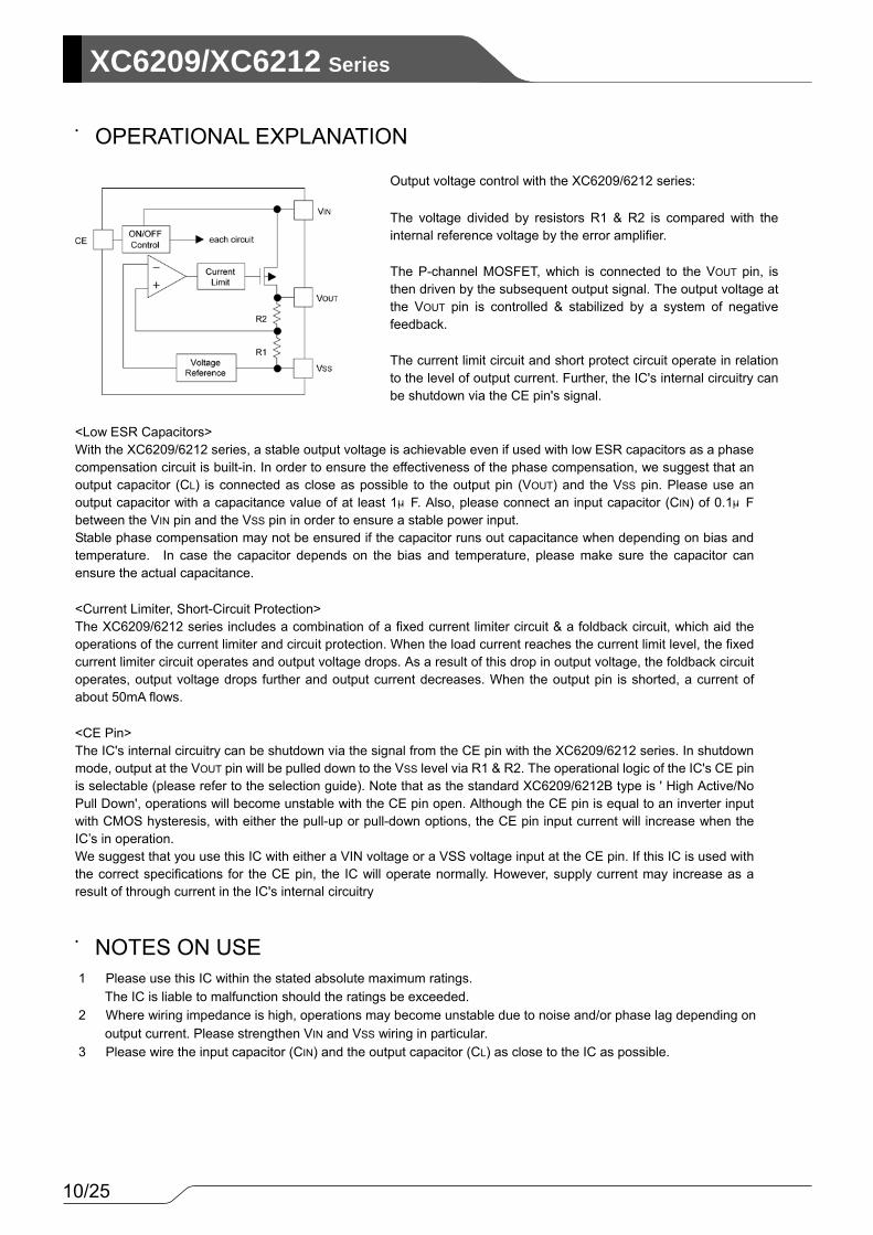
■OPERATIONAL EXPLANATION
Output voltage control with the XC6209/6212 series:
The voltage divided by resistors R1 & R2 is compared with the internal reference voltage by the error amplifier.
The P-channel MOSFET, which is connected to the VOUT pin, is then driven by the subsequent output signal. The output voltage at the VOUT pin is controlled & stabilized by a system of negative feedback.
The current limit circuit and short protect circuit operate in relation to the level of output current. Further, the IC's internal circuitry can be shutdown via the CE pin's signal.
<Low ESR Capacitors> With the XC6209/6212 series, a stable output voltage is achievable even if used with low ESR capacitors as a phase compensation circuit is built-in. In order to ensure the effectiveness of the phase compensation, we suggest that an output capacitor (CL) is connected as close as possible to the output pin (VOUT) and the VSS pin. Please use an output capacitor with a capacitance value of at least 1μF. Also, please connect an input capacitor (CIN) of 0.1μF between the VIN pin and the VSS pin in order to ensure a stable power input. Stable phase compensation may not be ensured if the capacitor runs out capacitance when depending on bias and temperature. In case the capacitor depends on the bias and temperature, please make sure the capacitor can ensure the actual capacitance.
<Current Limiter, Short-Circuit Protection> The XC6209/6212 series includes a combination of a fixed current limiter circuit & a foldback circuit, which aid the operations of the current limiter and circuit protection. When the load current reaches the current limit level, the fixed current limiter circuit operates and output voltage drops. As a result of this drop in output voltage, the foldback circuit operates, output voltage drops further and output current decreases. When the output pin is shorted, a current of about 50mA flows.
<CE Pin> The IC's internal circuitry can be shutdown via the signal from the CE pin with the XC6209/6212 series. In shutdown mode, output at the VOUT pin will be pulled down to the VSS level via R1 & R2. The operational logic of the IC's CE pin is selectable (please refer to the selection guide). Note that as the standard XC6209/6212B type is ' High Active/No Pull Down', operations will become unstable with the CE pin open. Although the CE pin is equal to an inverter input with CMOS hysteresis, with either the pull-up or pull-down options, the CE pin input current will increase when the IC’s in operation. We suggest that you use this IC with either a VIN voltage or a VSS voltage input at the CE pin. If this IC is used with the correct specifications for the CE pin, the IC will operate normally. However, supply current may increase as a result of through current in the IC's internal circuitry
■NOTES ON USE
11/25
XC6209/XC6212Series
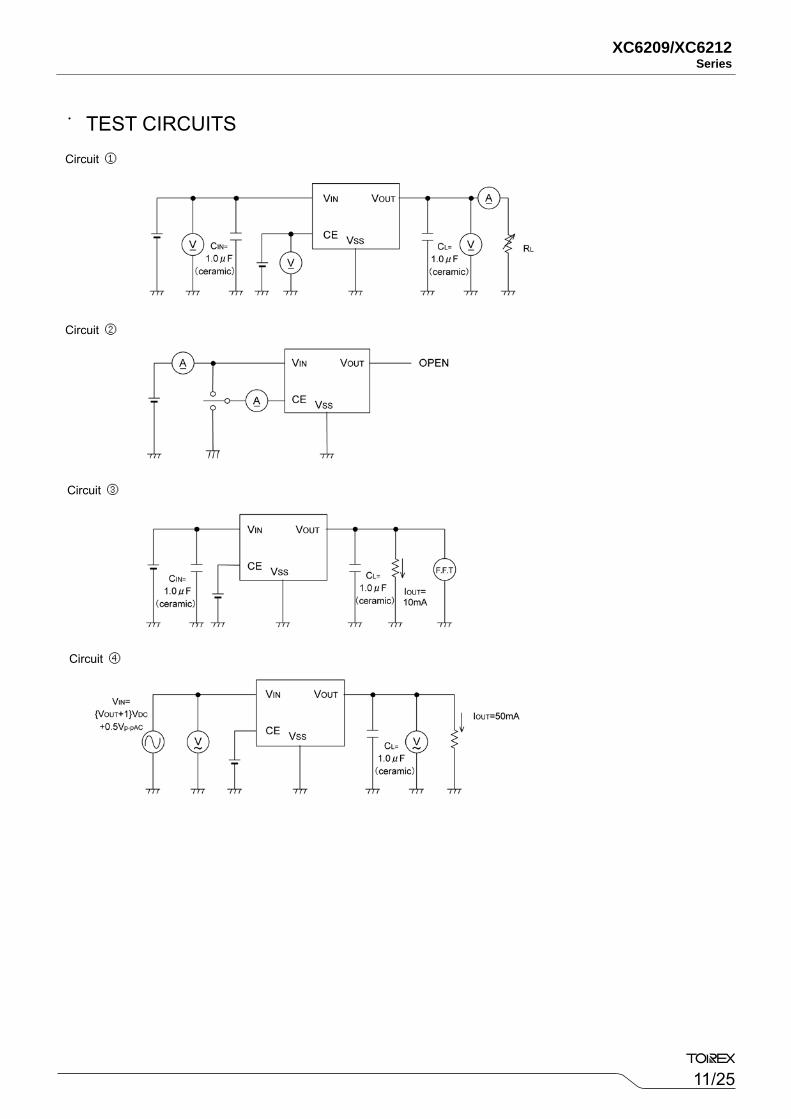
■TEST CIRCUITSCircuit ①
Circuit ③
Circuit ④
Circuit ②
12/25
XC6209/XC6212 Series
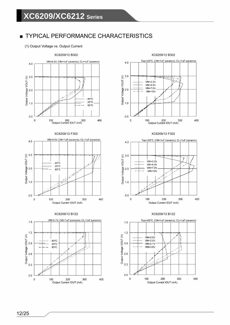
■TYPICAL PERFORMANCE CHARACTERISTICS (1) Output Voltage vs. Output Current
XC6209/12 B302 XC6209/12 B302
XC6209/12 F302 XC6209/12 F302
XC6209/12 B122 XC6209/12 B122
13/25
XC6209/XC6212Series
■TYPICAL PERFORMANCE CHARACTERISTICS (Continued)
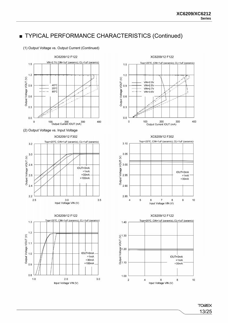
(1) Output Voltage vs. Output Current (Continued)
XC6209/12 F122 XC6209/12 F122
XC6209/12 F302 XC6209/12 F302
XC6209/12 F122 XC6209/12 F122
(2) Output Voltage vs. Input Voltage
14/25
XC6209/XC6212 Series
■TYPICAL PERFORMANCE CHARACTERISTICS (Continued)
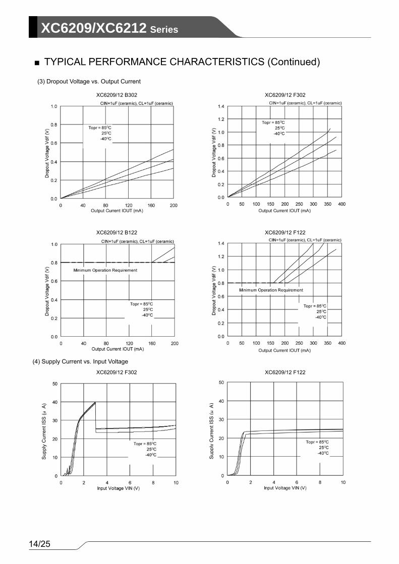
XC6209/12 B302 XC6209/12 F302
(3) Dropout Voltage vs. Output Current
XC6209/12 B122 XC6209/12 F122
XC6209/12 F302 XC6209/12 F122
(4) Supply Current vs. Input Voltage
Supp
ly C
urre
nt IS
S (μ
A)
Supp
ly C
urre
nt IS
S (μ
A)
15/25
XC6209/XC6212Series
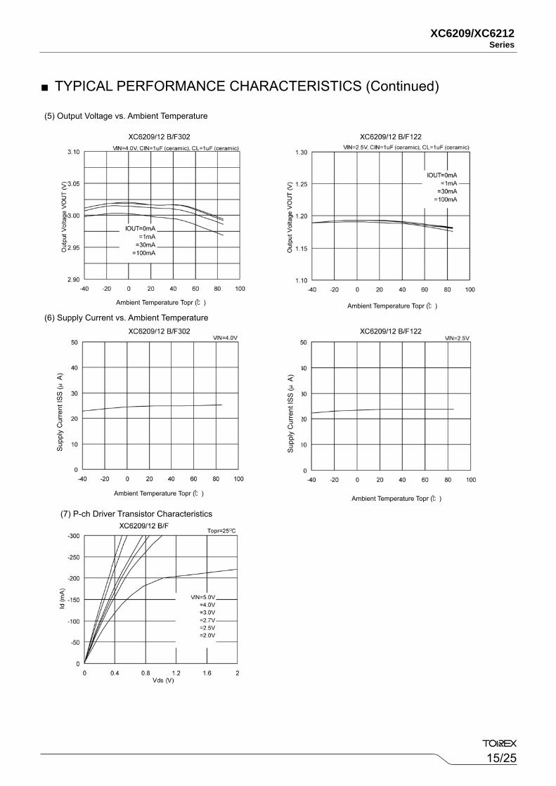
■TYPICAL PERFORMANCE CHARACTERISTICS (Continued)
(5) Output Voltage vs. Ambient Temperature
(6) Supply Current vs. Ambient Temperature
(7) P-ch Driver Transistor Characteristics
Supp
ly C
urre
nt IS
S (μ
A)
Supp
ly C
urre
nt IS
S (μ
A)
Ambient Temperature Topr (℃) Ambient Temperature Topr (℃)
Ambient Temperature Topr (℃) Ambient Temperature Topr (℃)
16/25
XC6209/XC6212 Series
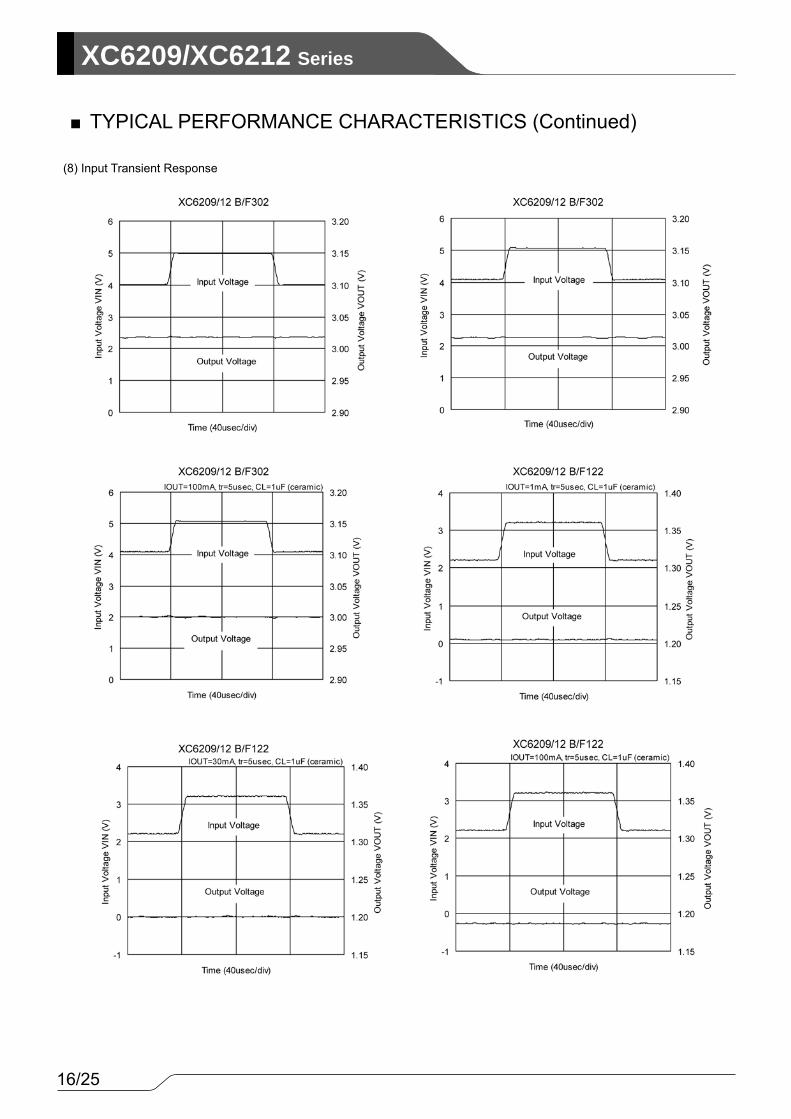
■TYPICAL PERFORMANCE CHARACTERISTICS (Continued)
(8) Input Transient Response
17/25
XC6209/XC6212Series
■TYPICAL PERFORMANCE CHARACTERISTICS (Continued)
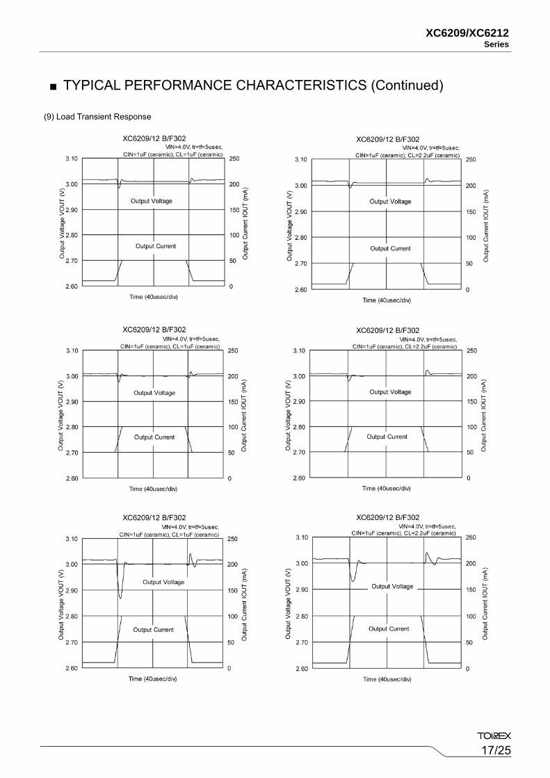
(9) Load Transient Response
18/25
XC6209/XC6212 Series
■TYPICAL PERFORMANCE CHARACTERISTICS (Continued)
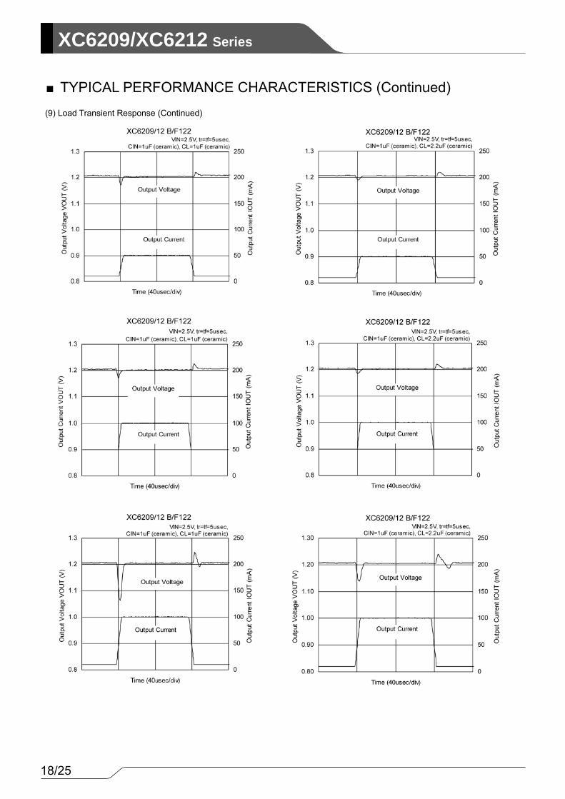
(9) Load Transient Response (Continued)
19/25
XC6209/XC6212Series
■TYPICAL PERFORMANCE CHARACTERISTICS (Continued)
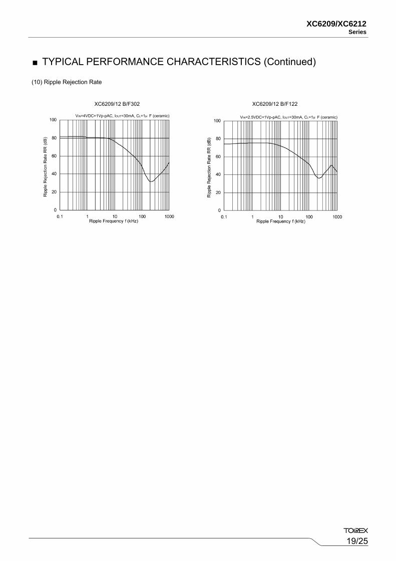
(10) Ripple Rejection Rate
VIN=4VDC+1Vp-pAC, IOUT=30mA, CL=1μF (ceramic)
XC6209/12 B/F302 XC6209/12 B/F122
VIN=2.5VDC+1Vp-pAC, IOUT=30mA, CL=1μF (ceramic)
20/25
XC6209/XC6212 Series
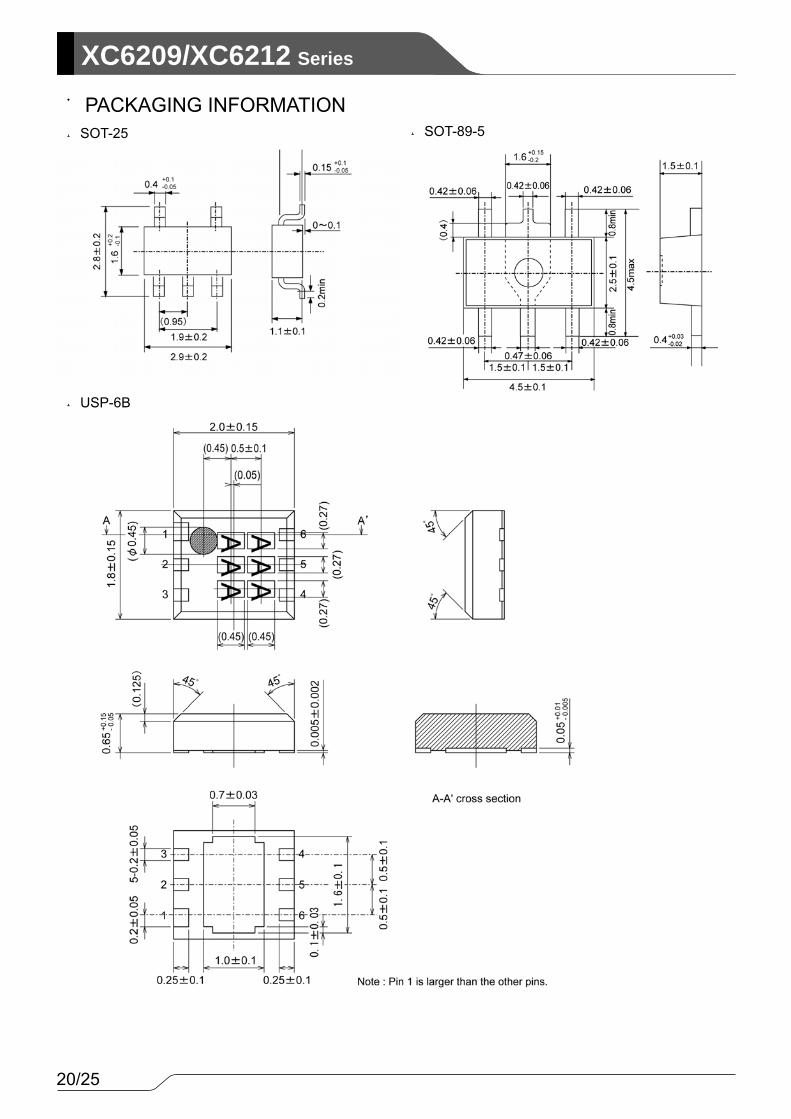
■PACKAGING INFORMATION●SOT-25
●USP-6B
●SOT-89-5
21/25
XC6209/XC6212Series
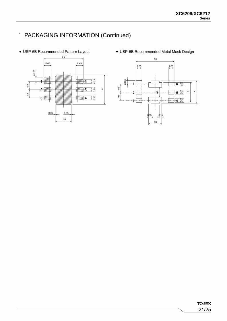
■PACKAGING INFORMATION (Continued)
●USP-6B Recommended Pattern Layout ●USP-6B Recommended Metal Mask Design
22/25
XC6209/XC6212 Series
MARK OUTPUT VOLTAGE (V) MARK OUTPUT VOLTAGE (V) 0 - 3.1 - 3.15 F 1.6 4.6 1.65 4.651 - 3.2 - 3.25 H 1.7 4.7 1.75 4.752 - 3.3 - 3.35 K 1.8 4.8 1.85 4.853 - 3.4 - 3.45 L 1.9 4.9 1.95 4.954 - 3.5 - 3.55 M 2.0 5.0 2.05 5.055 - 3.6 - 3.65 N 2.1 5.1 2.15 5.156 - 3.7 - .3.75 P 2.2 5.2 2.25 5.257 - 3.8 - 3.85 R 2.3 5.3 2.35 5.358 0.9 3.9 0.95 3.95 S 2.4 5.4 2.45 5.459 1.0 4.0 1.05 4.05 T 2.5 5.5 2.55 5.55A 1.1 4.1 1.15 4.15 U 2.6 5.6 2.65 5.65B 1.2 4.2 1.25 4.25 V 2.7 5.7 2.75 5.75C 1.3 4.3 1.35 4.35 X 2.8 5.8 2.85 5.85D 1.4 4.4 1.45 4.45 Y 2.9 5.9 2.95 5.95E 1.5 4.5 1.55 4.55 Z 3.0 6.0 3.05 -
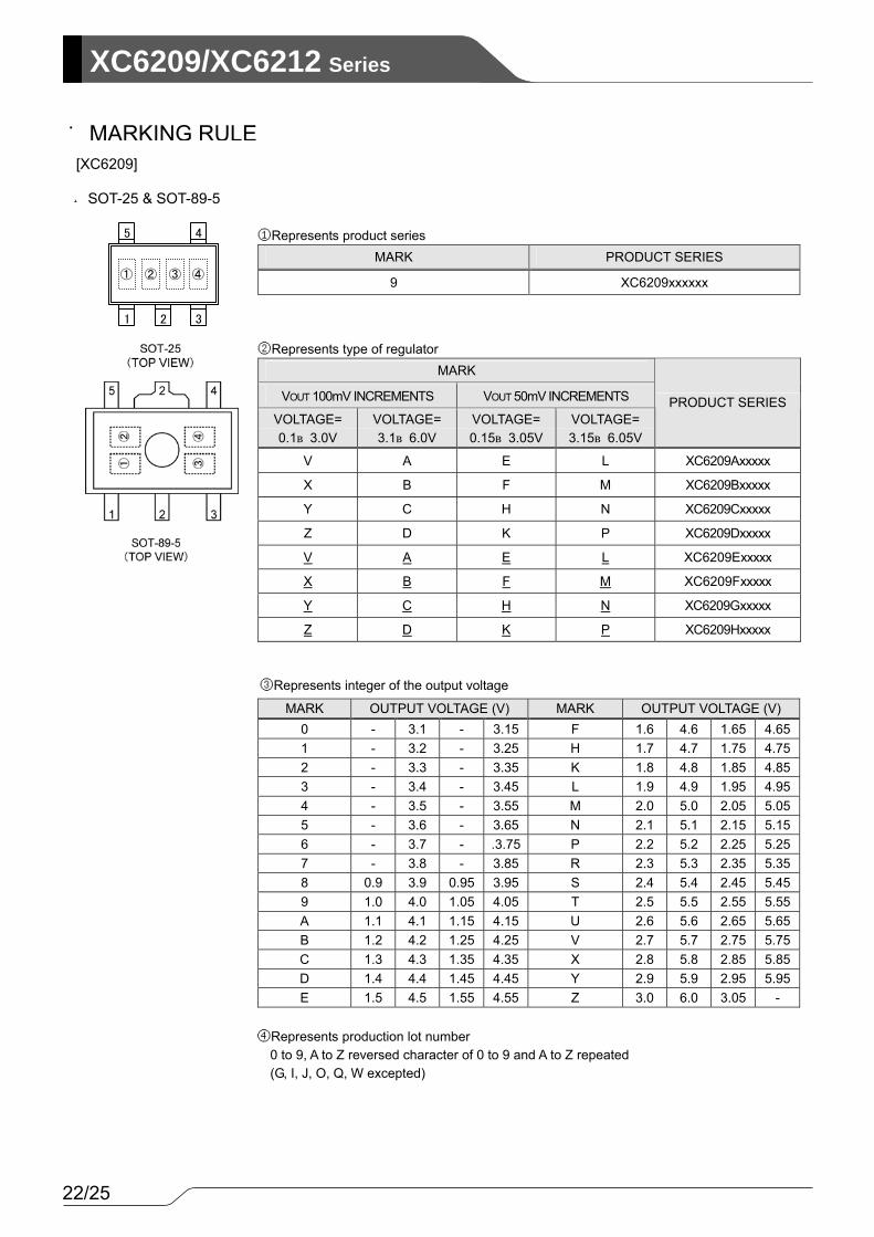
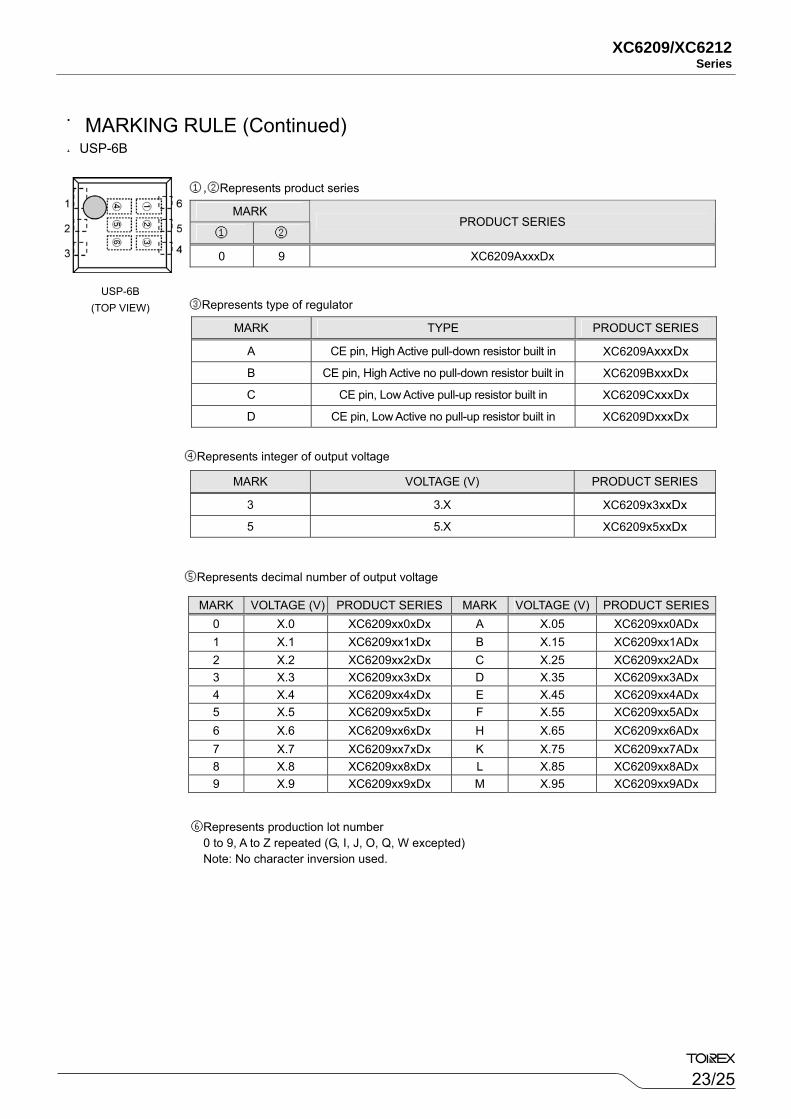
■MARKING RULE[XC6209]
●SOT-25 & SOT-89-5
①Represents product series MARK PRODUCT SERIES
9 XC6209xxxxxx
②Represents type of regulator MARK
VOUT 100mV INCREMENTS VOUT 50mV INCREMENTS
VOLTAGE= 0.1~3.0V
VOLTAGE= 3.1~6.0V
VOLTAGE= 0.15~3.05V
VOLTAGE= 3.15~6.05V
PRODUCT SERIES
V A E L XC6209Axxxxx
X B F M XC6209Bxxxxx
Y C H N XC6209Cxxxxx
Z D K P XC6209Dxxxxx
V A E L XC6209Exxxxx
X B F M XC6209Fxxxxx
Y C H N XC6209Gxxxxx
Z D K P XC6209Hxxxxx
③Represents integer of the output voltage
④Represents production lot number 0 to 9, A to Z reversed character of 0 to 9 and A to Z repeated (G, I, J, O, Q, W excepted)
① ② ③ ④
1 2 3
5 4
23/25
XC6209/XC6212Series
MARK
① ② PRODUCT SERIES
0 9 XC6209AxxxDx
MARK TYPE PRODUCT SERIES
A CE pin, High Active pull-down resistor built in XC6209AxxxDx
B CE pin, High Active no pull-down resistor built in XC6209BxxxDx
C CE pin, Low Active pull-up resistor built in XC6209CxxxDx
D CE pin, Low Active no pull-up resistor built in XC6209DxxxDx
MARK VOLTAGE (V) PRODUCT SERIES
3 3.X XC6209x3xxDx
5 5.X XC6209x5xxDx
MARK VOLTAGE (V) PRODUCT SERIES MARK VOLTAGE (V) PRODUCT SERIES0 X.0 XC6209xx0xDx A X.05 XC6209xx0ADx 1 X.1 XC6209xx1xDx B X.15 XC6209xx1ADx 2 X.2 XC6209xx2xDx C X.25 XC6209xx2ADx 3 X.3 XC6209xx3xDx D X.35 XC6209xx3ADx 4 X.4 XC6209xx4xDx E X.45 XC6209xx4ADx 5 X.5 XC6209xx5xDx F X.55 XC6209xx5ADx 6 X.6 XC6209xx6xDx H X.65 XC6209xx6ADx 7 X.7 XC6209xx7xDx K X.75 XC6209xx7ADx 8 X.8 XC6209xx8xDx L X.85 XC6209xx8ADx 9 X.9 XC6209xx9xDx M X.95 XC6209xx9ADx
●USP-6B
①,②Represents product series
③Represents type of regulator
④Represents integer of output voltage
⑤Represents decimal number of output voltage
⑥Represents production lot number 0 to 9, A to Z repeated (G, I, J, O, Q, W excepted)
Note: No character inversion used.
■MARKING RULE (Continued)
USP-6B (TOP VIEW)
24/25
XC6209/XC6212 Series
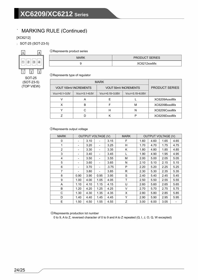
MARK PRODUCT SERIES
9 XC6212xxxMx
MARK
VOUT 100mV INCREMENTS VOUT 50mV INCREMENTS
VOUT=0.1~3.0V VOUT=3.1~6.0V VOUT=0.15~3.05V VOUT=3.15~6.05V
PRODUCT SERIES
V A E L XC6209AxxxMx
X B F M XC6209BxxxMx
Y C H N XC6209CxxxMx
Z D K P XC6209DxxxMx
MARK OUTPUT VOLTAGE (V) MARK OUTPUT VOLTAGE (V) 0 - 3.10 - 3.15 F 1.60 4.60 1.65 4.651 - 3.20 - 3.25 H 1.70 4.70 1.75 4.752 - 3.30 - 3.35 K 1.80 4.80 1.85 4.853 - 3.40 - 3.45 L 1.90 4.90 1.95 4.954 - 3.50 - 3.55 M 2.00 5.00 2.05 5.055 - 3.60 - 3.65 N 2.10 5.10 2.15 5.156 - 3.70 - .3.75 P 2.20 5.20 2.25 5.257 - 3.80 - 3.85 R 2.30 5.30 2.35 5.358 0.90 3.90 0.95 3.95 S 2.40 5.40 2.45 5.459 1.00 4.00 1.05 4.05 T 2.50 5.50 2.55 5.55A 1.10 4.10 1.15 4.15 U 2.60 5.60 2.65 5.65B 1.20 4.20 1.25 4.25 V 2.70 5.70 2.75 5.75C 1.30 4.30 1.35 4.35 X 2.80 5.80 2.85 5.85D 1.40 4.40 1.45 4.45 Y 2.90 5.90 2.95 5.95E 1.50 4.50 1.55 4.55 Z 3.00 6.00 3.05 -
[XC6212]
①Represents product series
④Represents production lot number 0 to 9, A to Z, reversed character of 0 to 9 and A to Z repeated (G, I, J, O, Q, W excepted)
SOT-25 (SOT-23-5) (TOP VIEW)
②Represents type of regulator
③Represents output voltage
■MARKING RULE (Continued)
●SOT-25 (SOT-23-5)
① ② ③ ④
1 2 3
5 4
25/25
XC6209/XC6212Series
1. The products and product specifications contained herein are subject to change without
notice to improve performance characteristics. Consult us, or our representatives
before use, to confirm that the information in this datasheet is up to date.
2. We assume no responsibility for any infringement of patents, patent rights, or other
rights arising from the use of any information and circuitry in this datasheet.
3. Please ensure suitable shipping controls (including fail-safe designs and aging
protection) are in force for equipment employing products listed in this datasheet.
4. The products in this datasheet are not developed, designed, or approved for use with
such equipment whose failure of malfunction can be reasonably expected to directly
endanger the life of, or cause significant injury to, the user.
(e.g. Atomic energy; aerospace; transport; combustion and associated safety
equipment thereof.)
5. Please use the products listed in this datasheet within the specified ranges.
Should you wish to use the products under conditions exceeding the specifications,
please consult us or our representatives.
6. We assume no responsibility for damage or loss due to abnormal use.
7. All rights reserved. No part of this datasheet may be copied or reproduced without the
prior permission of TOREX SEMICONDUCTOR LTD.