Embed Size (px)
Citation preview
EIC Detector R&D Progress Report: from December 2015 to July 2016
Project Name: eRD6, Proposal for detector R&D towards an EIC detector
Project Leader:
Brookhaven National Lab: Craig WoodyFlorida Tech: Marcus HohlmannINFN Trieste: Silvia Dalla TorreStony Brook University: Klaus Dehmelt, Thomas HemmickUniversity of Virginia: Kondo Gnanvo, Nilanga LiyanageWIS: Alexander MilovYale University: Richard Majka, Nikolai Smirnov
Date: June, 2016
Abstract
To be inserted. We might need to place some words regarding the newly extended consortium with INFN and WIS.
1
Past
What was planned for this period?
Brookhaven National Lab:
The primary goal for this period was to prepare the TPC/Cherenkov (TPCC) prototype detector for a test beam measurement at the Fermilab test beam facility, perform the beam test, and analyze the data. All of our work was done in collaboration with the group at Stony Brook University, headed by prof. Thomas Hemmick. The hit-list for preparing the detector initially involved making the field cage robust against sparks, and performing in lab measurements including reconstructing TPC tracks from cosmics, drift velocity, gain, charge spread, and charge attachment measurements, all using pure CF4, i.e., the detector gas to be used during the beam test. We also planned to make the photocathode for the Cherenkov portion of the detector, consisting of a GEM coated with CsI using a sophisticated evaporator system at Stony Brook. After fully assembling the TPCC with the new photocathode, we planned to transport the detector from Stony Brook to FNAL while under gas flow for the purpose of keeping the CsI quantum efficiency intact. Once the beam test is complete, we planned to carry out the data analysis in a collaborative manner with Stony Brook. Along the way, we also planned to develop online monitoring tools to do quick quality checks on measured tracks within the TPC and light yield measurements within the Cherenkov portion of the detector for the beam test. In addition, during this time, we started to design several variants of a new chevron readout pattern aimed at improved resolution performance, and hoped to have one particular design fabricated in time for use in the TPC portion of the prototype.
Florida Institute of Technology:
1. Finish our second paper on EIC R&D results and submit it to a peer-reviewed journal. The topic is a study of the geometric-mean method for determining the spatial resolution of tracking detectors in the presence of multiple scattering.
2. Analyze the BNL scan data for the zigzag readout boards obtained in Nov 2015.3. Before producing the new large zigzag readout board or foil for the next Forward
Tracker (FT) GEM prototype, demonstrate that the re-designed zigzag strips have a more linear response. To that end, produce new radial zigzag boards for a 10 cm × 10 cm GEM detector with the re-designed zigzag pattern and scan them at BNL.
4. Start producing the large common GEM foils and send out the designs for drift and readout foils and the various frames for quotes. Attempt to get them produced if feasible in the current 6 month time period. Investigate stiff carbon fiber frames for assembling the next EIC FT GEM prototype.
INFN Trieste:
N/A
Stony Brook University:
It was planned to refurbish the Big Mac evaporator after finalization of design consideration so that the necessary equipment for the mirror production can be purchased. The diameter of the vessel is about 7 feet and therefore would allow the insertion of large sized mirror blanks for evaporating with MgF2.
2
Another project was to design a pad readout board with snowflake pattern, locally at Stony Brook with engineers and aiming for placing an order to our previous PCB vendor.
University of Virginia:
1. Continue the tests of the Cr-GEM detector in x-ray box to study the performance under severe background conditions
2. Complete the design of the zebra-to-Panasonic adapter board and of the GEM frames and mechanical structure of the triple-GEM chamber
3. The new 2D U-V strips readout design with narrow strips present several advantages that are beneficial for EIC tracking detectors. However, a few new ideas such as etching the top and bottom strips contacts on the same Kapton support and the zebra connectors for electrical contacts need to be tested before we produce the EIC-size board for the second prototype. We plan to develop a small (10 × 10 cm2) 2D U-V strips readout board with the new zebra-based connection scheme and zebra-to-Panasonic adapter and perform validation tests.
Weizmann Institute of Science:
N/A
Yale University:
3-Coordinate GEM During the past period it was planned to complete the analysis.
Hybrid Gain Structure for TPC readout – 2 GEM plus Micromegas (2-GEM+MMG)During this period it was planned to submit a paper on the results achieved to date. It was also planned to continue study of 2-GEM+MMG with resistive planes. Further study to understand the corona like discharge at high intensity was planned.
Multi-element stacked gated gridContinued setup and characterization of the stacked gated grid was planned
3
What was achieved?
Brookhaven National Lab:
Beam Test Preparation
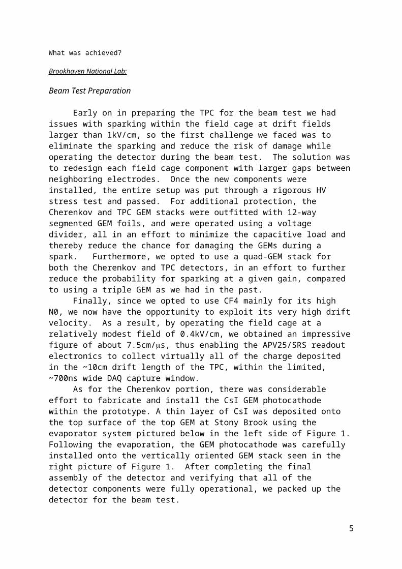
Early on in preparing the TPC for the beam test we had issues with sparking within the field cage at drift fields larger than 1kV/cm, so the first challenge we faced was to eliminate the sparking and reduce the risk of damage while operating the detector during the beam test. The solution was to redesign each field cage component with larger gaps between neighboring electrodes. Once the new components were installed, the entire setup was put through a rigorous HV stress test and passed. For additional protection, the Cherenkov and TPC GEM stacks were outfitted with 12-way segmented GEM foils, and were operated using a voltage divider, all in an effort to minimize the capacitive load and thereby reduce the chance for damaging the GEMs during a spark. Furthermore, we opted to use a quad-GEM stack for both the Cherenkov and TPC detectors, in an effort to further reduce the probability for sparking at a given gain, compared to using a triple GEM as we had in the past. Finally, since we opted to use CF4 mainly for its high N0, we now have the opportunity to exploit its very high drift velocity. As a result, by operating the field cage at a relatively modest field of 0.4kV/cm, we obtained an impressive figure of about 7.5cm/s, thus enabling the APV25/SRS readout electronics to collect virtually all of the charge deposited in the ~10cm drift length of the TPC, within the limited, ~700ns wide DAQ capture window. As for the Cherenkov portion, there was considerable effort to fabricate and install the CsI GEM photocathode within the prototype. A thin layer of CsI was deposited onto the top surface of the top GEM at Stony Brook using the evaporator system pictured below in the left side of Figure 1. Following the evaporation, the GEM photocathode was carefully installed onto the vertically oriented GEM stack seen in the right picture of Figure 1. After completing the final assembly of the detector and verifying that all of the detector components were fully operational, we packed up the detector for the beam test.
Fig. 1 Picture of the vacuum CsI evaporator at Stony Brook Univ. (left), and a CsI coated gold GEM foil, standing vertically inside a glove box with low water levels to keep the CsI intact (right).
4
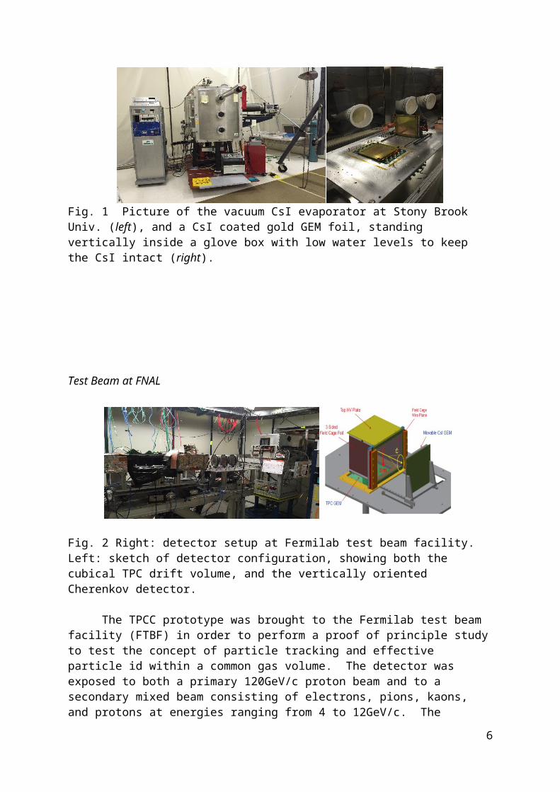
Test Beam at FNAL
Fig. 2 Right: detector setup at Fermilab test beam facility. Left: sketch of detector configuration, showing both the cubical TPC drift volume, and the vertically oriented Cherenkov detector.
The TPCC prototype was brought to the Fermilab test beam facility (FTBF) in order to perform a proof of principle study to test the concept of particle tracking and effective particle id within a common gas volume. The detector was exposed to both a primary 120GeV/c proton beam and to a secondary mixed beam consisting of electrons, pions, kaons, and protons at energies ranging from 4 to 12GeV/c. The prototype was also placed just downstream of a 12 layer Si telescope which was used to measure high resolution reference tracks for comparison with tracks measured in the TPC.
Cherenkov detector
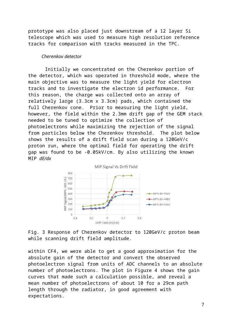
Initially we concentrated on the Cherenkov portion of the detector, which was operated in threshold mode, where the main objective was to measure the light yield for electron tracks and to investigate the electron id performance. For this reason, the charge was collected onto an array of relatively large (3.3cm x 3.3cm) pads, which contained the full Cherenkov cone. Prior to measuring the light yield, however, the field within the 2.3mm drift gap of the GEM stack needed to be tuned to optimize the collection of photoelectrons while maximizing the rejection of the signal from particles below the Cherenkov threshold. The plot below shows the results of a drift field scan during a 120GeV/c proton run, where the optimal field for operating the drift gap was found to be -0.05kV/cm. By also utilizing the known MIP dE/dx
Fig. 3 Response of Cherenkov detector to 120GeV/c proton beam while scanning drift field amplitude.
5
within CF4, we were able to get a good approximation for the absolute gain of the detector and convert the observed photoelectron signal from units of ADC channels to an absolute number of photoelectrons. The plot in Figure 4 shows the gain curves that made such a calculation possible, and reveal a mean number of photoelectrons of about 10 for a 29cm path length through the radiator, in good agreement with expectations.
410 420 430 440 450 460 470 480 49010
100
1000
10000
f(x) = 8.27245845151281E-11 exp( 0.062967052448368 x )f(x) = 1.77066215158974E-10 exp( 0.0635998786422317 x )
Gain Vs GEM dV
MPV (FB)Exponential (MPV (FB))MPV (RB)Exponential (MPV (RB))
dV [Volts]
Abso
lute
Gai
n
Fig. 4 Gain curves measured in 120GeV/c proton beam with the Cherenkov detector in forward bais (FB = 0.7kV/cm), and reverse bias (RB=-0.05kV/cm).
In addition, preliminary analysis of the Cherenkov data already shows a reasonable separation in the signal amplitude between particles above and below the Cherenkov threshold, as seen in Figure 5 below.
Fig. 5 Cherenkov detector pulse height distributions for 12GeV/c particles above and below the Cherenkov threshold for varying GEM voltages. The blue curve corresponds to electrons and pions, which are above the Cherenkov threshold and the red curve corresponds to kaons and protons.
6
GEM dV=475V
GEM dV=465VGEM dV=455V
TPC detector
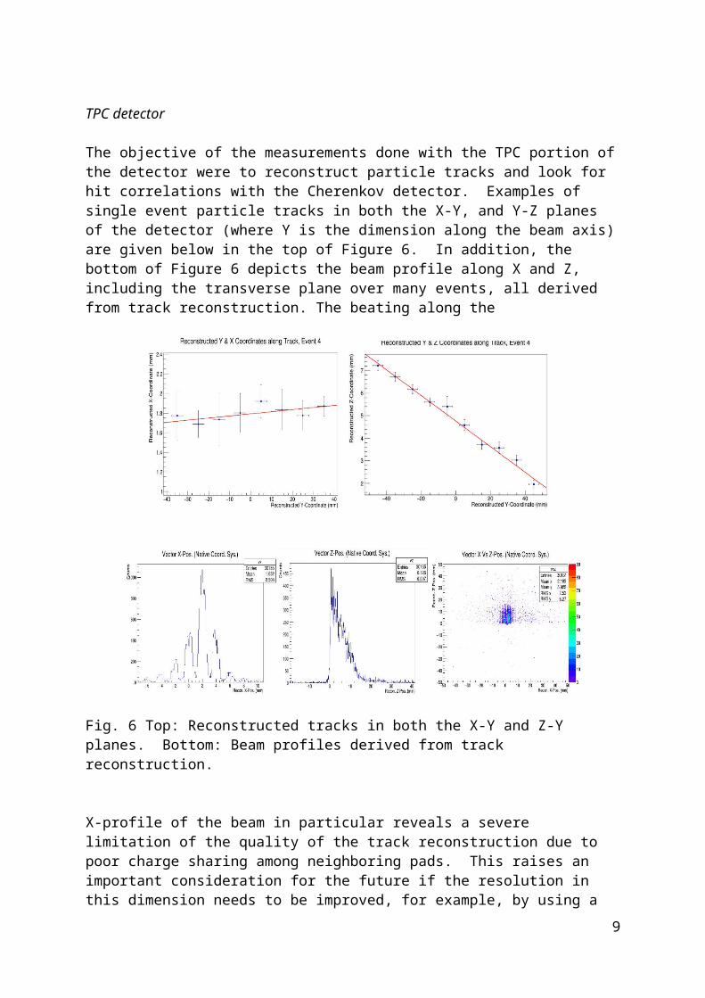
The objective of the measurements done with the TPC portion of the detector were to reconstruct particle tracks and look for hit correlations with the Cherenkov detector. Examples of single event particle tracks in both the X-Y, and Y-Z planes of the detector (where Y is the dimension along the beam axis) are given below in the top of Figure 6. In addition, the bottom of Figure 6 depicts the beam profile along X and Z, including the transverse plane over many events, all derived from track reconstruction. The beating along the
Fig. 6 Top: Reconstructed tracks in both the X-Y and Z-Y planes. Bottom: Beam profiles derived from track reconstruction.
X-profile of the beam in particular reveals a severe limitation of the quality of the track reconstruction due to poor charge sharing among neighboring pads. This raises an important consideration for the future if the resolution in this dimension needs to be improved, for example, by using a gas with enhanced transverse charge diffusion. As the analysis progresses, the resolution of the TPC tracks in both the X and Z dimensions will be determined by comparison to the Si reference tracks. So far, the correlation of the spatial coordinates of the Si and TC tracks is evidenced in the plot in Fig. 7 below.
7
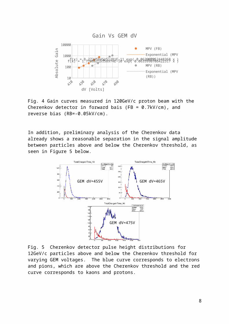
Fig. 7 Correlation plots for X and Y track coordinates, respectively for the TPC and Si detectors derived from vector reconstruction.
A significant improvement of this beam test compared to the previous one, done with the minidrift detector, is the that we measured the phase offset between the global beam trigger and the SRS DAQ clock edge, in order to enable a direct correction for the corresponding phase uncertainty. Finally, the plots in Fig. 8 nicely demonstrate the hit correlation between the Cherenkov and TPC detectors.
Fig. 8 3D event displays demonstrating the hit correlations between TPC tracks and the corresponding hits in the Cherenkov detector in the vertical plane (red: below threshold, green: above threshold).
The beam test was an overall success as these initial results indicate, and upon the completion of the analysis we will have more conclusive results as to the viability of this novel detector.
Florida Institute of Technology:
Publishing and Presenting R&D results
We submitted our paper “Accuracy of the geometric-mean method for determining spatial resolutions of tracking detectors in the presence of multiple Coulomb scattering” to the Journal of Instrumentation (JINST) and posted it on the e-print arXiv (1604.06130). This is our second paper that is an outcome of the first eRD6 beam test at FNAL.We also submitted an abstract on the “Study of non-linear response of a GEM read out with radial zigzag strips” to the 2016 IEEE NSS/MIC conference in Strasbourg, France.
8
Results on non-linearity of zigzag strip readouts from X-ray scans
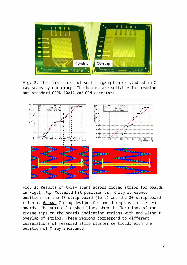
We scanned two zigzag-strip readout boards using a standard 10 cm by 10 cm triple-GEM detector and a collimated X-ray gun on a 2D motorized stage at BNL and analyzed the data. The patterns of the zigzag strips on these boards are identical to those implemented in the readout PCB of the first large 1-m GEM detector that we had tested at Fermilab and reported on earlier. The objective was to gain more information on the non-linear behavior of this readout type that was observed in the Fermilab data so that the design can be modified to produce a more linear behavior.As shown in Fig. 2, one board has 30 strips and the other one has 48 strips. The strips run radially with an azimuthal angle pitch of 1.37 mrad and they measure the azimuthal phi-coordinate of incident particles. The difference between the two boards is that the radial zigzag strips are located at different radii. Specifically, the radial range for the 48-strip (30-strip) board is about 1420-1520 mm (2240-2340 mm) corresponding to the narrow (wide) end of our first large-area prototype chamber.
Fig. 2: The first batch of small zigzag boards studied in X-ray scans by our group. The boards are suitable for reading out standard CERN 10×10 cm2 GEM detectors.
9
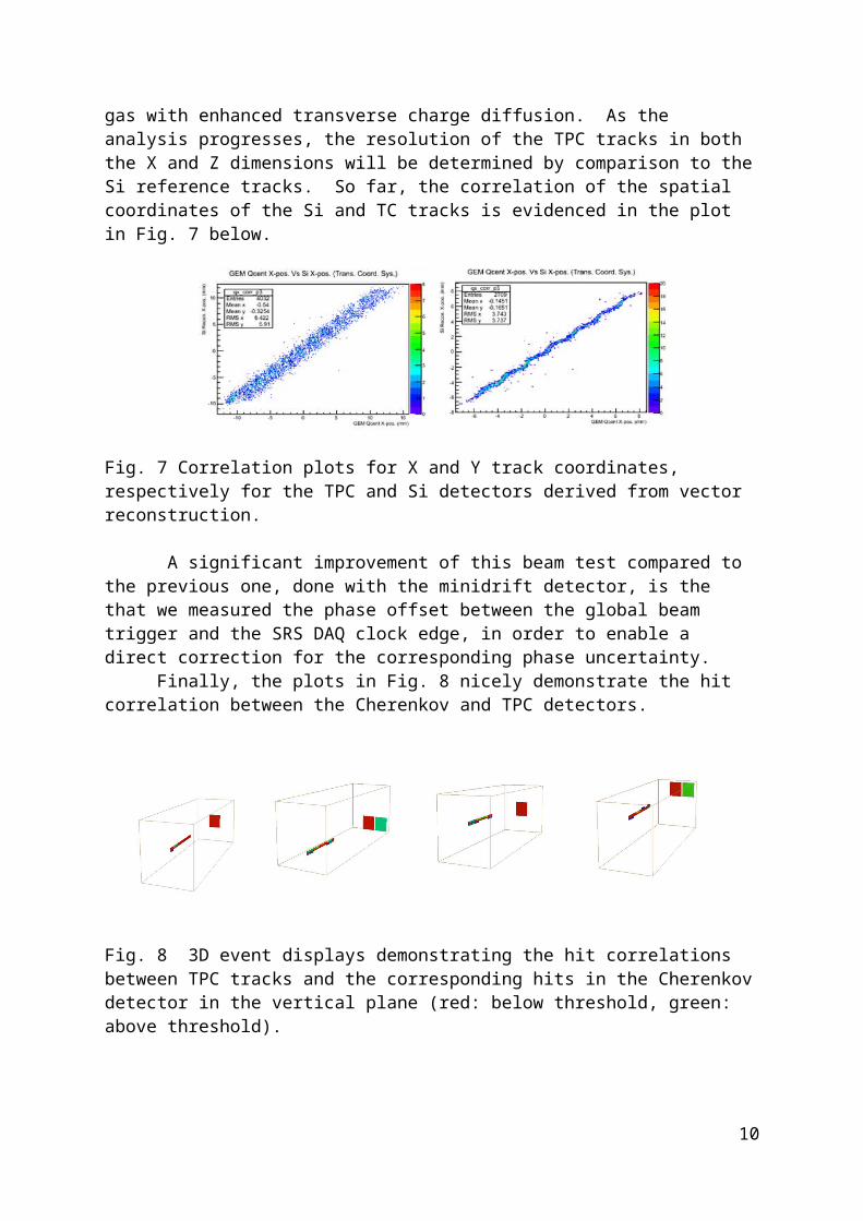
Fig. 3: Results of X-ray scans across zigzag strips for boards in Fig.1. Top: Measured hit position vs. X-ray reference position for the 48-strip board (left) and the 30-strip board (right). Bottom: Zigzag design of scanned regions on the two boards. The vertical dashed lines show the locations of the zigzag tips on the boards indicating regions with and without overlap of strips. These regions correspond to different correlations of measured strip cluster centroids with the position of X-ray incidence.
Fig. 3 (top) shows the measured hit position versus the position of incident X-rays for the two boards from the scans across zigzag strips. We observe in the scans that the measured hit position is not linearly related to the X-ray gun position, i.e. there is a non-linear response of the zigzag strips. In particular, the curves have some flat regions where the readout is not very sensitive to the incident particle position because only one strip is fired in those regions; the obtained hit position is then just the center of the strip as no charge is shared between strips. This is confirmed by inspecting the scanned positions on the boards (Fig. 3, bottom) as well as by checking the strip multiplicity of the charge clusters (Fig. 4).
Fig. 4: Mean cluster size vs. X-ray position for the 48-strip board (left) and 30-strip board (right) from the X-ray scans across zigzag strips.
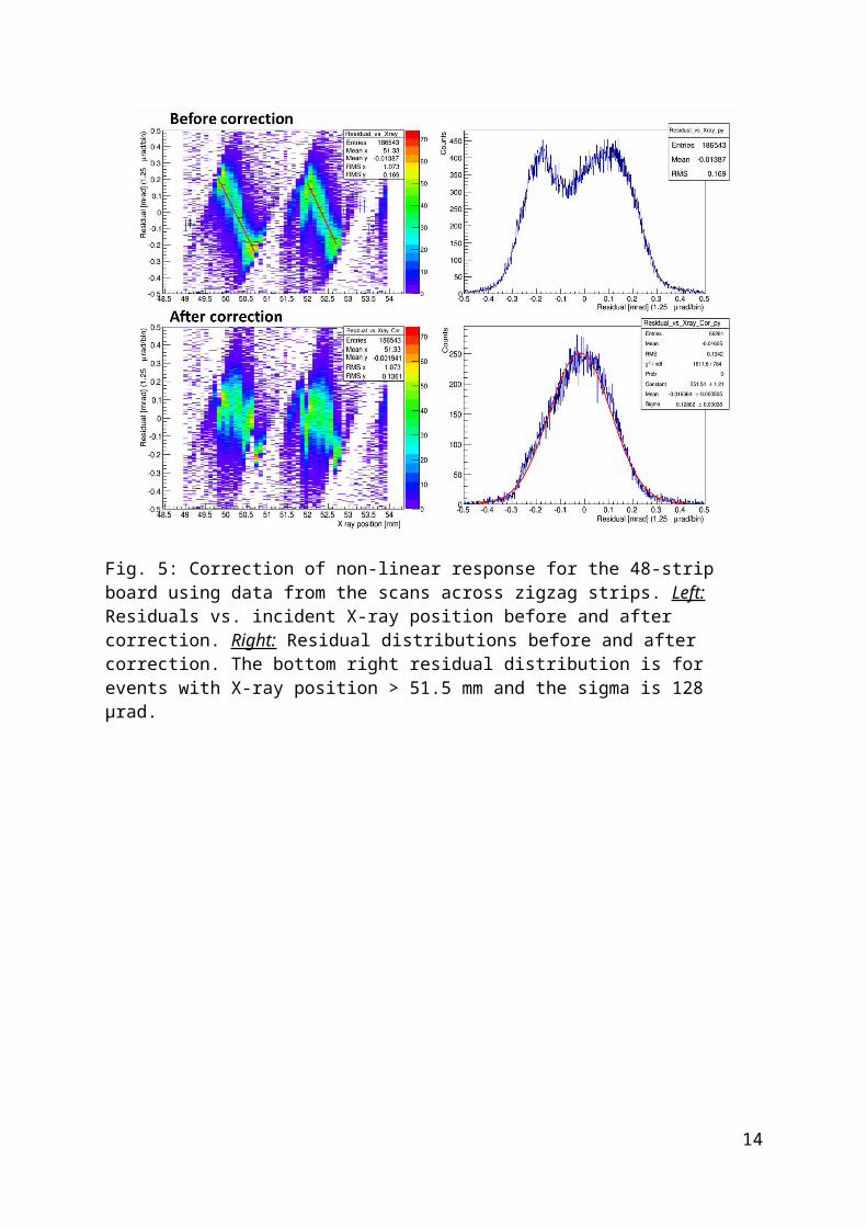
We correct the non-linear response offline using the data. For example, for the 48-strip board, we plot the residuals of the linear fits in Fig.3 vs. X-ray position and get global correction functions by fitting the resulting profiles (Fig. 5, top left). Plotting globally corrected residuals vs. X-ray position (Fig. 5, bottom left), we observe that the overall residual distribution improves (Fig. 5, right). For example, if we select events at X-ray positions larger than 51.5 mm, the observed residual sigma is about 128 μrad (Fig. 5, bottom right).
10
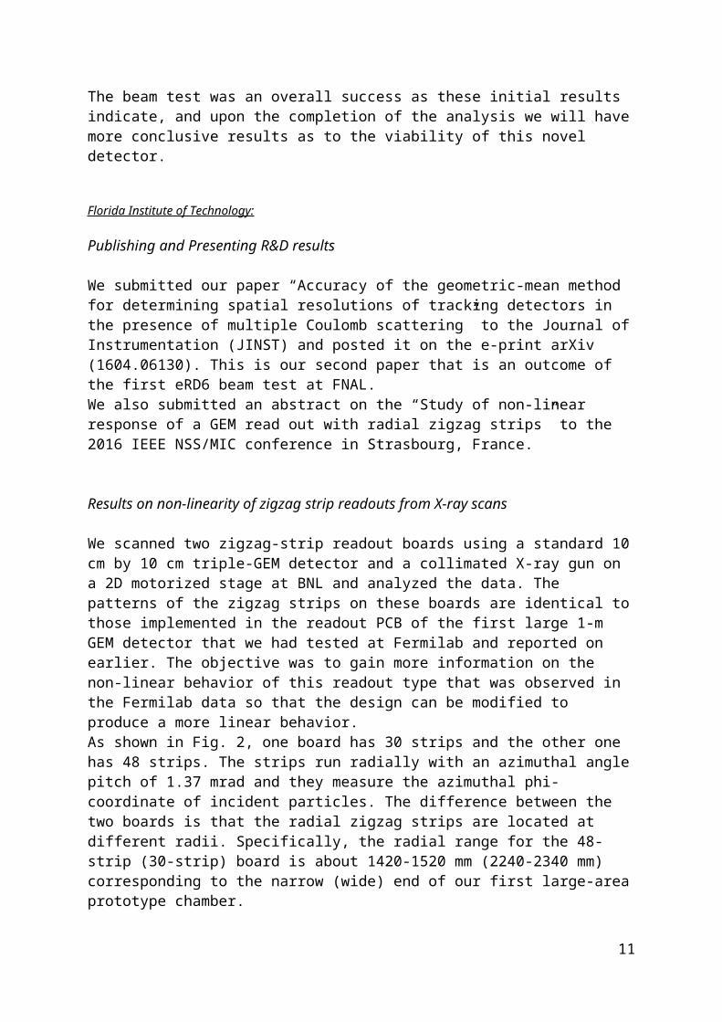
Fig. 5: Correction of non-linear response for the 48-strip board using data from the scans across zigzag strips. Left: Residuals vs. incident X-ray position before and after correction. Right: Residual distributions before and after correction. The bottom right residual distribution is for events with X-ray position > 51.5 mm and the sigma is 128 μrad.
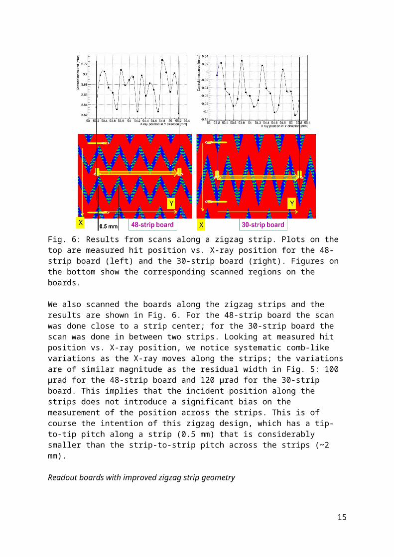
Fig. 6: Results from scans along a zigzag strip. Plots on the top are measured hit position vs. X-ray position for the 48-strip board (left) and the 30-strip board (right). Figures on the bottom show the corresponding scanned regions on the boards.
11
We also scanned the boards along the zigzag strips and the results are shown in Fig. 6. For the 48-strip board the scan was done close to a strip center; for the 30-strip board the scan was done in between two strips. Looking at measured hit position vs. X-ray position, we notice systematic comb-like variations as the X-ray moves along the strips; the variations are of similar magnitude as the residual width in Fig. 5: 100 μrad for the 48-strip board and 120 μrad for the 30-strip board. This implies that the incident position along the strips does not introduce a significant bias on the measurement of the position across the strips. This is of course the intention of this zigzag design, which has a tip-to-tip pitch along a strip (0.5 mm) that is considerably smaller than the strip-to-strip pitch across the strips (~2 mm).
Readout boards with improved zigzag strip geometry
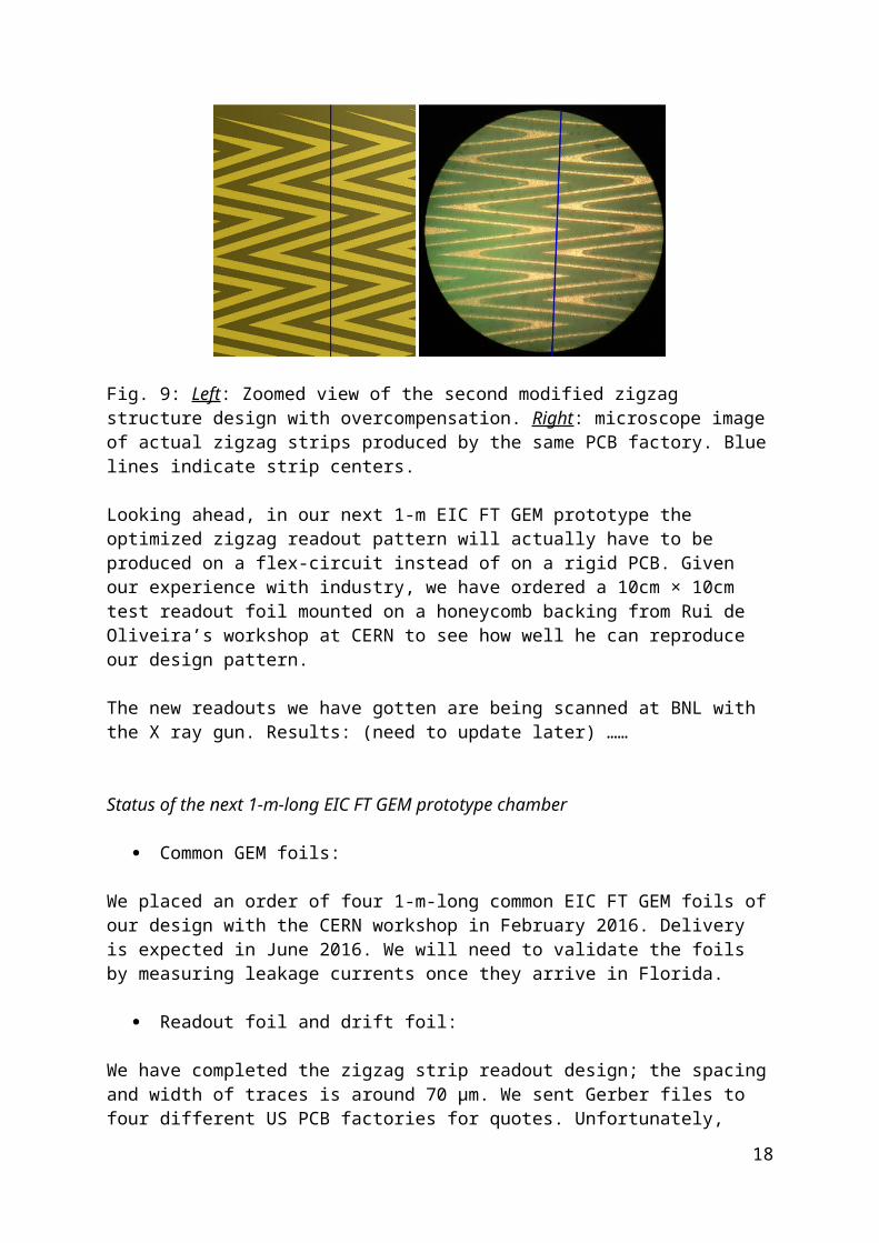
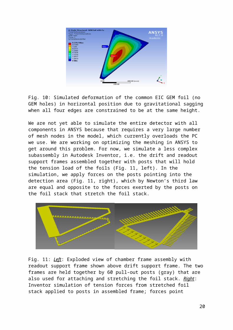
In the particular designs of the original two zigzag boards discussed above, the “zigs” and “zags” of a strip interleave with its neighboring strips only to a certain extent (Fig. 7). Much of the center region of each strip is not covered by adjacent strips and this explains that only one strip fires when a particle hits that region (Fig. 4). In the actual physical PCB implementation of this design, this flaw is exacerbated due to a rounding of sharp tips and troughs in the etching process (Fig. 7, right).In order to reduce the non-linear response of the zigzag strips due to this flaw in the strip geometry, we have modified the geometry of the zigzag structures so that the tips of the “zigs” and “zags” of a strip reach all the way to the centers of its neighboring strips (Fig. 8, left). At the same time, the tip-to-tip pitch of 0.5 mm is maintained. However, it appears that PCB industry has some difficulties to produce exactly what we have designed. The “zigs” and “zags” of the actual physical strips on the PCB do not fully reach the centers of neighboring strips (Fig. 8, right). Also, the strips come out much thinner than in the design. Consequently, we made a third design where the “zigs” and “zags” go even beyond the centers of neighboring strips (Fig. 9, left) in the hope that this would compensate for the production process and give us a PCB with the desired design. The resulting PCB produced by the same company comes close to the desired interleaving of zigs and zags; interestingly, the compensation in the design resulted in a slight overcompensation on the actual PCB (Fig. 9, right). However, strips are still coming out much thinner than designed. The company has suggested that this problem might be overcome by using a thinner copper layer on the PCB that requires less etching. We will continue working with the company to see if they can produce a PCB as we have designed it.
12
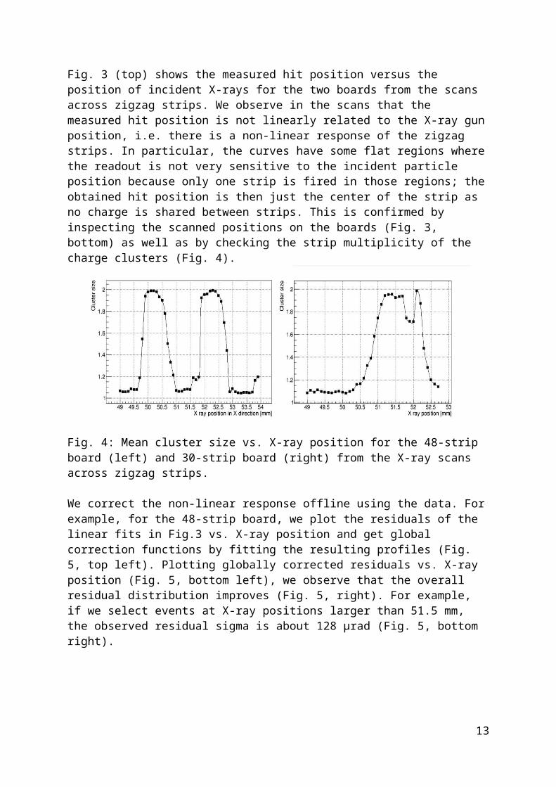
Fig. 7: Left: Zoomed view of a few readout strips in our original zigzag design. Right: Actual zigzag strips produced by a PCB factory. Blue lines indicate strip centers.
Fig. 8: Left: Zoomed view of the first modified zigzag structure design. Right: microscope image of actual zigzag strips produced by a PCB factory. Blue lines indicate strip centers.
Fig. 9: Left: Zoomed view of the second modified zigzag structure design with overcompensation. Right: microscope image of actual zigzag strips produced by the same PCB factory. Blue lines indicate strip centers.
13
Looking ahead, in our next 1-m EIC FT GEM prototype the optimized zigzag readout pattern will actually have to be produced on a flex-circuit instead of on a rigid PCB. Given our experience with industry, we have ordered a 10cm × 10cm test readout foil mounted on a honeycomb backing from Rui de Oliveira’s workshop at CERN to see how well he can reproduce our design pattern.
The new readouts we have gotten are being scanned at BNL with the X ray gun. Results: (need to update later) ……
Status of the next 1-m-long EIC FT GEM prototype chamber
Common GEM foils:
We placed an order of four 1-m-long common EIC FT GEM foils of our design with the CERN workshop in February 2016. Delivery is expected in June 2016. We will need to validate the foils by measuring leakage currents once they arrive in Florida.
Readout foil and drift foil:
We have completed the zigzag strip readout design; the spacing and width of traces is around 70 μm. We sent Gerber files to four different US PCB factories for quotes. Unfortunately, none of these factories is able to produce 1-meter-long flex PCB with the precision that is required. Then we approached the CERN workshop again and found that Rui Oliveira is able to produce this readout foil for us. We worked with his design team to tune and finalize the design. As mentioned above, in order to make sure that we can actually get produced what we have in the design, we asked Rui to first produce a small board for testing purposes. If the small CERN foil can be validated for our purposes, we will place the order for the full-size readout foil. We would then expect to receive that foil in August 2016. The much more straight-forward drift foil design is also finished. We have obtained quotes for both readout foil and drift foil from Rui.
Mechanical aspects of chamber construction and assembly:
As described in previous progress reports, we have adopted a modified mechanical stretching method without spacers that the CMS GEM collaboration has been using for large GEM chamber construction. In order to reduce material in the active detection area of the EIC FT prototype, we make a stack from five foils (three GEM foils, one drift foil, and one readout foil), sandwich it between two support frames made from some stiff material, and stretch the stack against so-called pull-out posts that are fixed on the support frames.
We completed the details of the 3D mechanical design for the prototype chamber in Autodesk Inventor by adding screws and nuts into the design. We are currently studying the expected deformations of this design with finite-element analyses using Autodesk Inventor and ANSYS. The reason to use ANSYS is that we found that Inventor cannot handle a stress analysis for thin foils. With help from our mechanical engineering department we have gained access to an ANSYS research license. We use these tools to define the required mechanical strengths and dimensions of support frames, screws, and other mechanical elements. We also study the expected deformation of the foils after stretching, e.g. under
14
gravitational load (Fig. 10), so that we can optimize the force loads that are applied in the stretching process.
Fig. 10: Simulated deformation of the common EIC GEM foil (no GEM holes) in horizontal position due to gravitational sagging when all four edges are constrained to be at the same height.
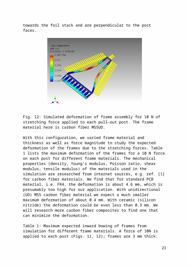
We are not yet able to simulate the entire detector with all components in ANSYS because that requires a very large number of mesh nodes in the model, which currently overloads the PC we use. We are working on optimizing the meshing in ANSYS to get around this problem. For now, we simulate a less complex subassembly in Autodesk Inventor, i.e. the drift and readout support frames assembled together with posts that will hold the tension load of the foils (Fig. 11, left). In the simulation, we apply forces on the posts pointing into the detection area (Fig. 11, right), which by Newton’s third law are equal and opposite to the forces exerted by the posts on the foil stack that stretch the foil stack.
Fig. 11: Left: Exploded view of chamber frame assembly with readout support frame shown above drift support frame. The two frames are held together by 60 pull-out posts (gray) that are also used for attaching and stretching the foil stack. Right: Inventor simulation of tension forces from stretched foil stack applied to posts in assembled frame; forces point towards the foil stack and are perpendicular to the post faces.
15
Fig. 12: Simulated deformation of frame assembly for 10 N of stretching force applied to each pull-out post. The frame material here is carbon fiber M55UD.
With this configuration, we varied frame material and thickness as well as force magnitude to study the expected deformation of the frames due to the stretching forces. Table 1 lists the maximum deformation of the frames for a 10 N force on each post for different frame materials. The mechanical properties (density, Young’s modulus, Poisson ratio, shear modulus, tensile modulus) of the materials used in the simulation are researched from internet sources, e.g. ref. [1] for carbon fiber materials. We find that for standard PCB material, i.e. FR4, the deformation is about 4.6 mm, which is presumably too high for our application. With unidirectional (UD) M55 carbon fiber material we expect a much smaller maximum deformation of about 0.4 mm. With ceramic (silicon nitride) the deformation could be even less than 0.3 mm. We will research more carbon fiber composites to find one that can minimize the deformation.
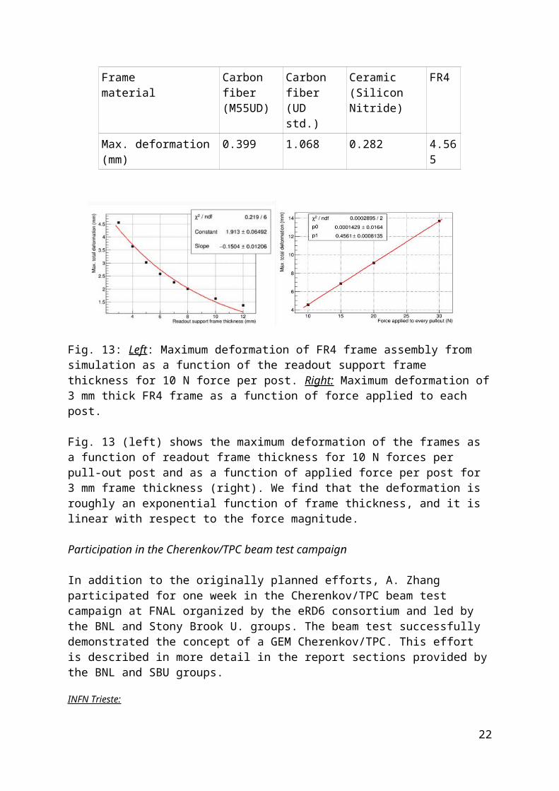
Table 1: Maximum expected inward bowing of frames from simulation for different frame materials. A force of 10N is applied to each post (Figs. 11, 12); frames are 3 mm thick.
Frame material
Carbon fiber (M55UD)
Carbon fiber (UD std.)
Ceramic (Silicon Nitride)
FR4
Max. deformation (mm) 0.399 1.068 0.282 4.565
16
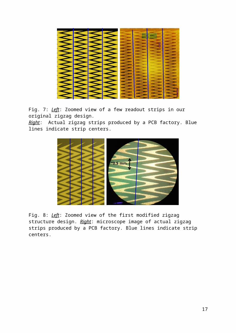
Fig. 13: Left: Maximum deformation of FR4 frame assembly from simulation as a function of the readout support frame thickness for 10 N force per post. Right: Maximum deformation of 3 mm thick FR4 frame as a function of force applied to each post.
Fig. 13 (left) shows the maximum deformation of the frames as a function of readout frame thickness for 10 N forces per pull-out post and as a function of applied force per post for 3 mm frame thickness (right). We find that the deformation is roughly an exponential function of frame thickness, and it is linear with respect to the force magnitude.
Participation in the Cherenkov/TPC beam test campaign
In addition to the originally planned efforts, A. Zhang participated for one week in the Cherenkov/TPC beam test campaign at FNAL organized by the eRD6 consortium and led by the BNL and Stony Brook U. groups. The beam test successfully demonstrated the concept of a GEM Cherenkov/TPC. This effort is described in more detail in the report sections provided by the BNL and SBU groups.
INFN Trieste:
N/A
Stony Brook University:
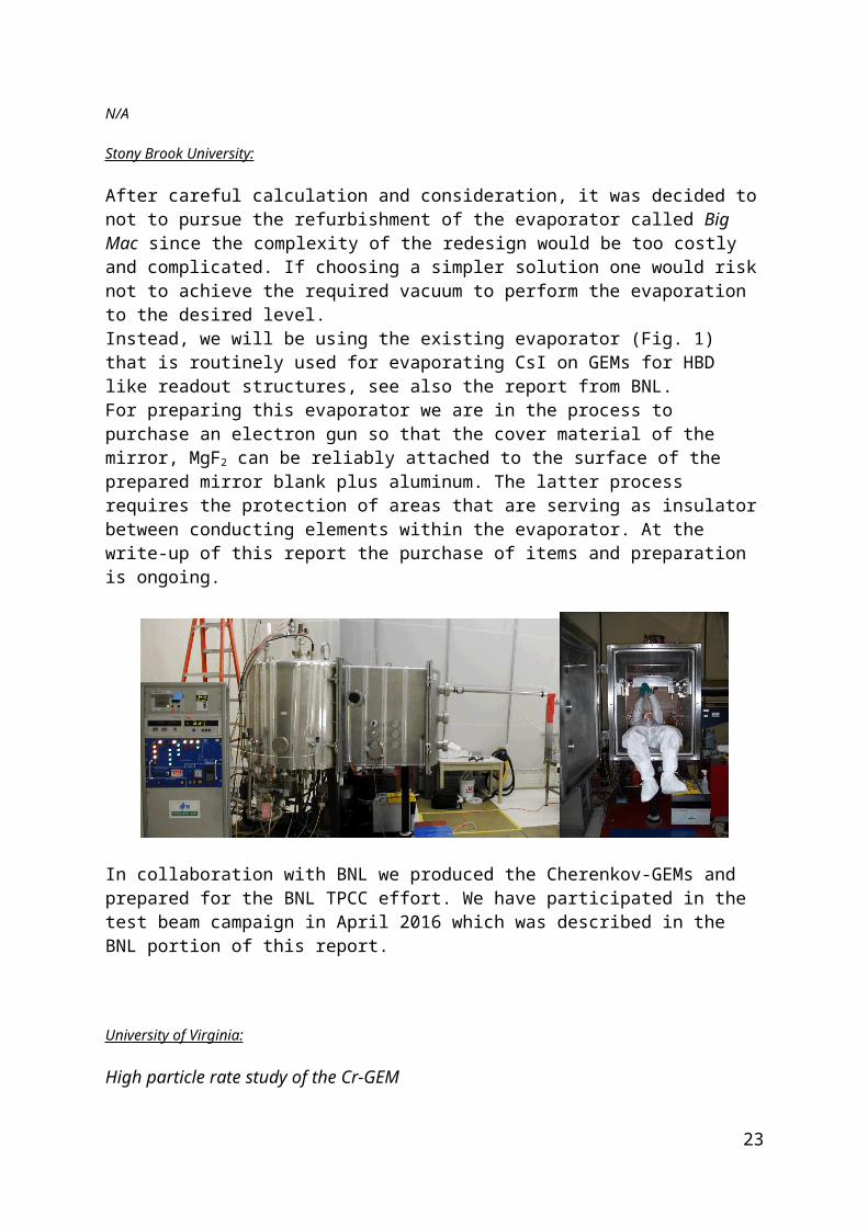
After careful calculation and consideration, it was decided to not to pursue the refurbishment of the evaporator called Big Mac since the complexity of the redesign would be too costly and complicated. If choosing a simpler solution one would risk not to achieve the required vacuum to perform the evaporation to the desired level.Instead, we will be using the existing evaporator (Fig. 1) that is routinely used for evaporating CsI on GEMs for HBD like readout structures, see also the report from BNL.For preparing this evaporator we are in the process to purchase an electron gun so that the cover material of the mirror, MgF2 can be reliably attached to the surface of the prepared mirror blank plus aluminum. The latter process requires the protection of areas that are serving as insulator between conducting elements within the evaporator. At the write-up of this report the purchase of items and preparation is ongoing.
In collaboration with BNL we produced the Cherenkov-GEMs and prepared for the BNL TPCC effort. We have participated in the test beam campaign in April 2016 which was described in the BNL portion of this report.
17
University of Virginia:
High particle rate study of the Cr-GEM
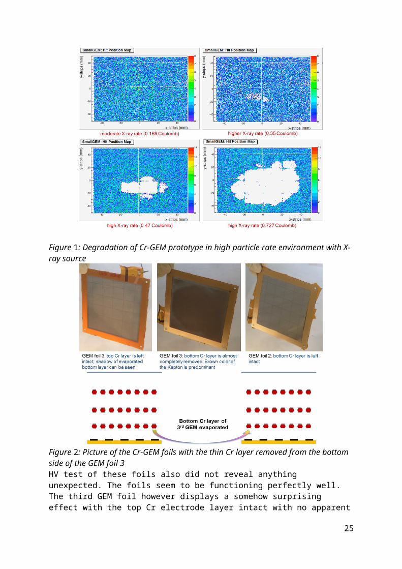
The Cr-GEM concept would allow the reduction of GEM detector material thickness by a factor of two. Our results indicate that the Cr-GEM detectors work very well under low particle rate, while extreme particle fluxes appear to damage some components of the detector. Our observations show that a similar detector with some re configuration may be able to function well under high fluxes.The study consists of a uniform exposure of the Cr-GEM in the high intensity x-ray source to analyse the response of the chamber such as uniformity and efficiency for various particle rates. For each measurement, the total charge (Coulombs) integrated over 24 hours is used as a measure of the particle rate. The top left hit map plot of Figure 1 shows no degradation of the chamber after an exposition to moderate particle rate an integrated charge of about 0.17 C. With an increase of the intensity of the x-ray source corresponding to an accumulated current of 0.35 C in 24 hours, we observe the appearence of a small dead area spot as shown on the top right plot. The dead area size increases dramatically with increasing rate as shown on the bottom two plots of Figure 1, with almost half of the active area of the chamber dead when the rate increases up to .7 C a day. We opened the Cr-GEM prototype in the clean room to inspect the individual GEM foils after the intense high rate test and subsequent efficiency drop. Preliminary visual inspection shows that the first two GEM foils seem intact with no noticeable damage due to the high rate irradiation.
Figure 1: Degradation of Cr-GEM prototype in high particle rate environment with X-ray source
18

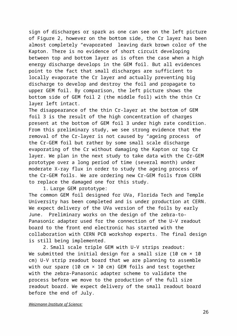
Figure 2: Picture of the Cr-GEM foils with the thin Cr layer removed from the bottom side of the GEM foil 3HV test of these foils also did not reveal anything unexpected. The foils seem to be functioning perfectly well. The third GEM foil however displays a somehow surprising effect with the top Cr electrode layer intact with no apparent sign of discharges or spark as one can see on the left picture of Figure 2, however on the bottom side, the Cr layer has been almost completely “evaporated” leaving dark brown color of the Kapton. There is no evidence of short circuit developing between top and bottom layer as is often the case when a high energy discharge develops in the GEM foil. But all evidences point to the fact that small discharges are sufficient to locally evaporate the Cr layer and actually preventing big discharge to develop and destroy the foil and propagate to upper GEM foil. By comparison, the left picture shows the bottom side of GEM foil 2 (the middle foil) with the thin Cr layer left intact. The disappearance of the thin Cr-layer at the bottom of GEM foil 3 is the result of the high concentration of charges present at the bottom of GEM foil 3 under high rate condition. From this preliminary study, we see strong evidence that the removal of the Cr-layer is not caused by “ageing process” of the Cr-GEM foil but rather by some small scale discharge evaporating of the Cr without damaging the Kapton or top Cr layer. We plan in the next study to take data with the Cr-GEM prototype over a long period of time (several month) under moderate X-ray flux in order to study the ageing process of the Cr-GEM foils. We are ordering new Cr-GEM foils from CERN to replace the damaged one for this study.
1. Large GEM prototype: The common GEM foil designed for UVa, Florida Tech and Temple University has been completed and is under production at CERN. We expect delivery of the UVa version of the foils by early June. Preliminary works on the design of the zebra-to-Panasonic adapter used for the connection of the U-V readout board to the front end electronic has started with the collaboration with CERN PCB workshop experts. The final design is still being implemented.
2. Small scale triple GEM with U-V strips readout: We submitted the initial design for a small size (10 cm × 10 cm) U-V strip readout board that we are planning to assemble with our spare (10 cm × 10 cm) GEM foils and test together with the zebra-Panasonic adapter scheme to validate the process before we move to the
19
production of the full size readout board. We expect delivery of the small readout board before the end of July.
Weizmann Institute of Science:
N/A
Yale University:
3-Coordinate GEMExperienced personnel were added to this effort and the analysis is near completion. The final pad response functions are being extracted to develop the required corrections.
Hybrid Gain Structure for TPC readout – 2 GEM plus MicromegasA paper on the results to date has been submitted to NIM and is available at: http://arxiv.org/abs/1603.08473Results and status were also presented atRD51 Collaboration Meeting (08-11 March 2016), CERN, Combined of Gas Electron Multipliers and Micromegas as Gain Elements in a High Rate Time Projection ChamberandECFA LC workshop, May 30th – June 5th, 2016, Santander (Spain); Invited report; Combined of Gas Electron Multipliers and Micromegas as Gain Elements in a High Rate Time Projection Chamber
Consulting with other groups it was determined that the high intensity corona-like discharges seen in the resistive layer MMG’s are a problem with the manufacture of the resistive layers for the particular chambers we have. We will submit these for rebuild.
Multi-element stacked gated gridInitial measurements to determine voltages needed for transparency and ion clearing are completed.
20
What was not achieved?
Brookhaven National Lab:
As mentioned, alongside bench testing the TPCC, we designed a new chevron readout pattern for the TPC and hoped to have it installed in time for the beam test in April. It turns out that this hope was too ambitious as the design was not completed early enough for us to be able to have it fabricated in time to test and install it in the detector, before departing for Fermilab. Moving forward, we plan to complete the design of a variety of promising chevron patterns, guided by simulation, have them fabricated and then tested in our lab. The lab setup consists of a collimated x-ray gun mounted to a precision X-Y stage that moves the source a known distance, which is then compared to the reconstructed position, to provide a measure of the position resolution. Though these tests may not be as effective as testing the boards in a beam test, comparing the performance of the various designs under similar conditions in the lab will allow us to attach an absolute figure of merit to each design.
Florida Institute of Technology:
We achieved most of what we had planned for this period.
We were slowed down somewhat on the production of the zigzag readout for the large FT GEM prototype because the production of test boards with proper zigzag strips to understand the non-linear response is more difficult than anticipated. We are addressing this issue with the PCB company and with the CERN workshop.
We have not yet been able to experimentally investigate stiff chamber frames, e.g. made from carbon fiber; we have just started investigating this issue in the finite-element simulations.
INFN Trieste:
N/A
Stony Brook University:
As described above the evaporator Big Mac was not refurbished and instead the redesign of the existing CsI evaporating facility is ongoing.The design of a snowflake readout pad had been postponed due to the support activity of the TPCC effort of BNL.
University of Virginia:
a It has taken longer than expected to get funding transferred from BNL to UVa. The final paperwork for fund transfer has been submitted to BNL and we are now waiting for funds to arrive at UVa.
a The design of the support frames for the GEM foils and the mechanical structure of the detector is a few months behind schedule. This was in part due to our other commitment to the PRad experiment run at JLab that just started in May 13, 2013. Our detector group at UVa was in charge of the construction, commissioning and installation in Hall B a JLab and operation of the large PRad GEM chambers as well as its readout electronics. Preparation for the PRad experiment required that we focus our resources for the last 6 months or so on the PRad GEM detectors. We will resume the drawing and design of the frames in the coming weeks.
21
a For the same reasons as state above, our plan to test the small size U-V readout board with zebra connection has been delayed as well. We have just managed during this cycle to finalize the drawings and place the order. We expect to receive the board in about a month for now and we would then start the validation test of the new ideas.
Weizmann Institute of Science:
N/A
Yale University:
3-Coordinate GEMSubmission of a paper on the final analysis remains to be completed.
Hybrid Gain Structure for TPC readout – 2 GEM plus MicromegasStudy of the resistive layer 2-GEM+MMG was delayed by an apparent problem with the manufacture of the MMG we have.
22
Future
What is planned for the next funding cycle and beyond? How, if at all, is this planning different from the original plan?
Brookhaven National Lab:
Our planned activities during the next funding cycle are as follows:
Complete the analysis of the TPCC test beam data and publish the results in IEEE TNS: The anticipated outcome from this test is that we demonstrate a proof of principle of the concept behind this hybrid detector, and include several import performance specifications such at the track position resolution of the TPC, and the light yield and eid performance of the Cherenkov portion of the detector.
Simulation/Design/Testing of new chevron patterns: Our colleagues at BNL are working to fully simulate the propagation of charge through the TPC, from the point where the primary charge is deposited in the gas volume to the point where the shaper response of the readout electronics is analyzed from each chevron pad. The effects of diffusion, the avalanche process, and the specific electric field shape in the GEM holes and near the readout electrodes are all taken into account in three dimensional space in an effort to accurately simulate the response of a variety of readout patterns. These results would then be used to guide design specs, for instance the periodicity and pitch of the chevron, to maximize resolution with minimal instrumentation. Finally, we plan to test each of the candidate chevron designs in the lab, as described above.
Working with Stony Brook to build TPC prototype field cage (hardware): Stony Brook has already initiated designing and building a portion of a prototype TPC field cage for use at EIC. The BNL group plans to aid the Stony Brook effort in any way that we can, though we cannot state specifics at this point.
Working with Stony Brook on Ion Back-Flow (IBF) measurements: A critical component for the successful operation of the TPC is to understand the magnitude of ion back flow to be expected in the TPC and to minimize it. These measurements will mainly deal with testing a new idea for shielding IBF in a multi-GEM readout, which entails operating the top GEM at a gain of one and applying a field in the first transfer gap in order to impose minimum fluctuations on the charge as is passes through the GEM. At the same time, the transparency of field lines through the top GEM should be minimal, thus cutting the IBF tremendously.
Work with Stony Brook to measure reflectivity of VUV mirrors: Stony Brook plans to produce high quality Al/MgF2 coated mirrors for future RICH detectors. We will use the VUV spectrometer at BNL in order to measure the reflectivity of these mirrors. However, the spectrometer requires new hardware, commissioning, and possibly new software before this measurement may be performed, which we anticipate should only take a few weeks to complete.
23

Florida Institute of Technology:
1. We will finish the tests of small zigzag boards to find the zigzag geometry with the most linear position response. We plan to publish the results from this study, most likely in the 2016 NSS IEEE proceedings. We will also apply that optimal geometry to the design of the large readout foil for the FT GEM prototype chamber and then have that foil produced at CERN.
2. We will measure leakage currents of the large common GEM foils once we receive them to assure the foil quality.
3. We need to finish the static structural FE analysis for the mechanical aspect of chamber assembly, specifically with respect to any potential for buckling of the frames under stretching forces, choose proper materials (frames, support boards, etc.), and then identify companies in industry that can produce them for us.
4. We expect to have the second FT GEM prototype chamber assembled by early 2017 so that we can test it in a beam at Fermilab in 2017.
INFN Trieste:
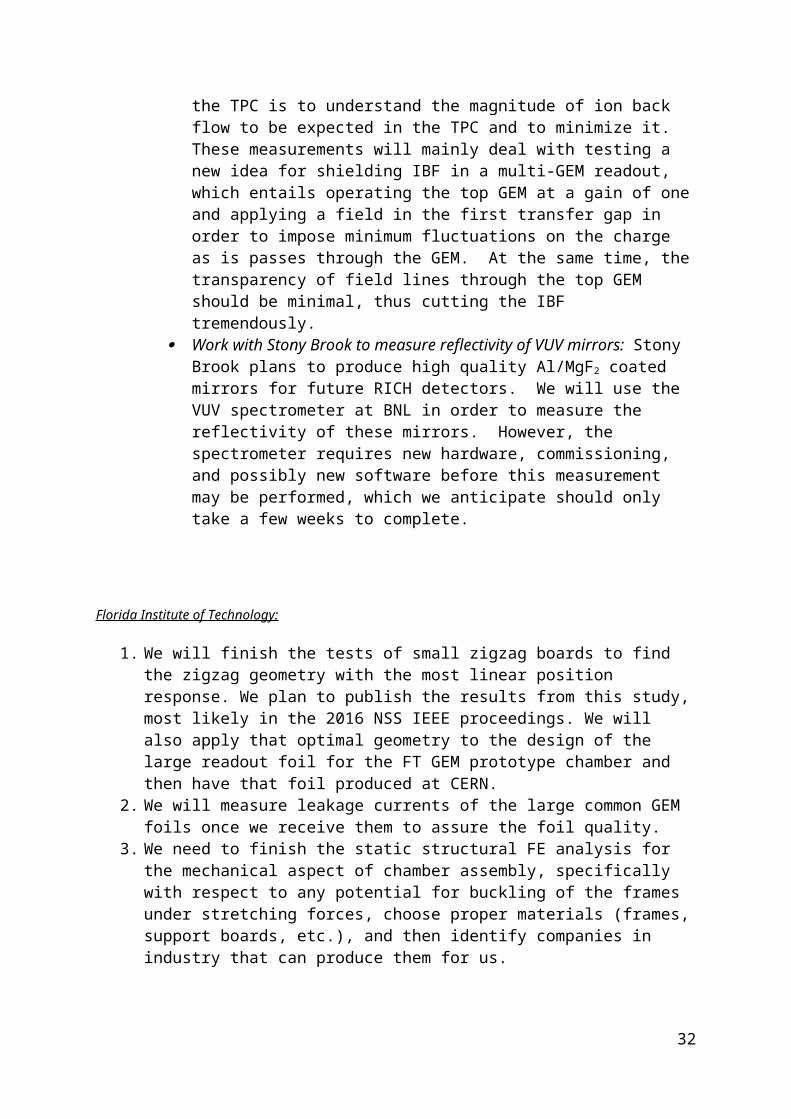
Further development of hybrid MPGDs for single photon detection synergic to TPC read-out sensors.
The concept of the hybrid MPGD detector of single photons has been developed in an eight-year R&D program; the reference figures for the present optimization are the requirement for the upgrade of the gaseous RICH counter of the COMPASS experiment at CERN SPS. The resulting detectors are presently built and installed, while the commissioning will start in the late Spring 2016. The detector architecture (Fig. 1) consists in three multiplication stages: two THick GEMs (THGEM) layers, the first one coated with a CsI film and acting as photocathode, followed by a MicroMegas (MM) multiplication stage. The two THGEMs are staggered: this configuration is beneficial both to reduce the Ion BackFlow (IBF) and to increase the maximum gain at which the detector can be operated exhibiting full electrical
stability. These photon detectors can operate at gains of at least 5 x 10⁴ and exhibit an IBF rate lower than 5%. The gas mixtures used are by Ar and CH4, with a rich methane fraction in order to maximize the photoelectron extraction.
24
Figure 1 – Schematic architecture of the hybrid MPGD detector of single photons (not to scale).
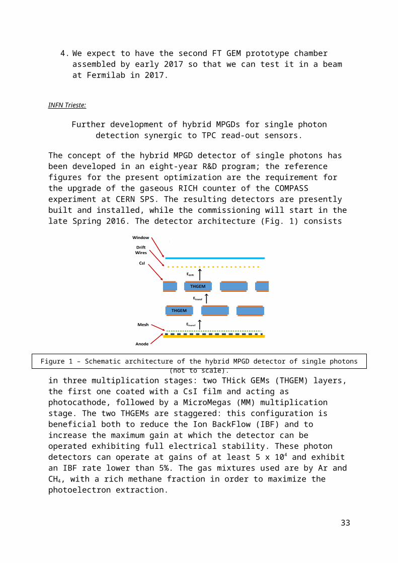
An original element of the hybrid MPGD photon detector is the approach to a resistive MM by discrete elements (Fig. 2), which has been triggered by the resistive MM developed for the ATLAS experiment at CERN LHC [The ATLAS Collaboration, "Technical Design Report for the New Small Wheel," CERN-LHCC-2013-006 / ATLAS-TDR-020, June 2013], but presents substantial differences. The anode elements (pads) facing the micromesh are individually equipped with large-value resistors and the HV is provided, via these resistors, to the anode electrodes, while the micromesh is grounded. A second set of electrodes (pads parallel to the first ones) are embedded in the anode PCB: the signal is transferred by capacitive coupling to these electrodes, which are connected to the front-end read-out electronics. The advantages of the design shortly described above are several:
As in ATLAS resistive MM, applying the HV to the anode instead of to the MM cathode results in larger amplitude signals;
In case of local defects of the MM, a single electrode can be isolated resulting in a dead area as large as the electrode itself, while the large majority of the detector is still active;
No resistive coating is present inside the detector volume; The absence of a resistive layer on top of the anode electrodes is limiting the
degradation of the dE/dx information in the collected signals.
25
Figure 2 – The resistive MM by discrete elements. (a) The principle is illustrated by a single pad; the different layer of the PCB forming the MM anode are schematically shown: the blue pad is the anode electrode of the MM kept at positive voltage; it directly faces the micromesh; the red pad is embedded in the PCB and the signal is transferred from the blue to the red pad by capacitive coupling. (b) The principle is illustrated by the electrical scheme: the top elements of the capacitors are the pad forming the MM anode (blue pad in (a)), the bottom elements of the capacitors (red pad in (a)) are connected to the front-end electronics. (c) Picture of the MM anode PCB in the present version, front view: the pad size is 8 x 8 mm2. (d) Picture of the MM anode PCB in the present version, rear view, detail: the connectors serving 48 pads are grouped together; both the signal connectors and the supports of the resistor arrays are present.
The hybrid detector concept can be further improved in order to match the requirements of high momenta hadron identification at EIC; this challenging task requires:
i. Limited radiator length of the order of 1 m: here one of the most promising approaches is the window-less RICH concept [M. Blatnik et al., IEEE transaction on Nuclear Science 62 (2015) 3256];
ii. Fine space granularity to cope with the modest lever arm related to the radiator length;iii. Control of the IBF rate in order to guarantee stable detector performance over time;iv. Further improvement in the engineering aspects in order to simplify the construction
and control the costs;v. The comparison between hybrid detectors where THGEMs or GEMS in view of an
overall optimization of the detector principle.The R&D program proposed here is meant to match the requirements listed above. It spans three years of activity and it includes five tasks:
1. test of novel materials for THGEM substrate to simplify the detector construction, increase the yield of valid large-size THGEMs and, thus, control the detector costs (related to requirement iv);
2. the development of resistive MM by discrete elements with miniaturized pad size (present size: 8 x 8 mm2) in order to obtain finer space resolution (related to requirement ii);
3. comparison of THGEM vs GEM photocathodes in order to select the best architecture for the photon detectors of the EIC RICH (related to requirement v);
4. further studies in order to enhance the IFB suppression in hybrid MPGDs (related to requirement iii);
5. operation of hybrid MPGDs (THGEMs + MM) in fluorocarbon-rich gas mixtures (related to requirement i).
The overall timelines are provided in Fig. 3.
It is relevant to underline that the further development of the hybrid detector concept, in particular with finer space resolution and low IBF rate is synergic to another sector of great relevance for the future experiments at EIC, namely the read-out sensors for the TPC. A hybrid MPGD approach to TPC read-out has already been proposed making use of traditional non-resistive MMs [A. Aiola et al., “Combination of two Gas Electron Multipliers and a Micromegas as gain elements for a time projection chamber”, http://arxiv.org/abs/1603.08473, submitted to Nucl. Instr. Meth. A]; our approach to resistive MM can offer a detector which exhibits robust electrical stability while preserving a good dE/dx resolution.
26
Figure 3 – Timelines of the R&D activity.
TASK no TASK1st
quarter2nd
quarter3rd
quarter4th
quarter1st
quarter2nd
quarter3rd
quarter4th
quarter1st
quarter2nd
quarter3rd
quarter4th
quarter
1 test of novel materials for THGEM
2resistive MM by discrete elements with miniaturized pad size
3comparison of THGEM vs GEM photocathodes
4enhancement of the IFB suppression in hybrid MPGDs
5operation of hybrid MPGDs (THGEMs + MM) in fluorocarbon-rich gas mixtures
FY 2017 FY 2018 FY 2019
Stony Brook University:
The finalization of redesigning the evaporator for producing large mirrors is expected to be finalized at the beginning of the new funding cycle. The plan is to provide a large surface equipped with smaller mirror blanks at each corner and in the center. The samples will then be evaluated with the VUV spectrometer from BNL. This should represent a good measure of the properties of a large mirror evaporation.Furthermore, data analysis for the TPCC beam test data from April will be performed.In collaboration with the BNL group we are planning to work on the understanding of the magnitude of ion back flow in a TPC and plan to purchase necessary equipment and test it under test beam condition.
University of Virginia:
For the coming cycle from June 2016 to December 2016, we plan to:a Continue the study of Cr-GEM detector with x-ray source. Take data under
moderate particle rate for several months to study the long term stability and ageing of such thin Cr-GEM structures.
a We plan to validate the new ideas such as etching the top and bottom strips contacts on the same Kapton support and the zebra connectors for electrical contacts developed for U-V strips readout of EIC GEM prototype II, on a small scale (10 cm × 10 cm) readout prototype before we move ahead with the full size detector.
a Upon reception of the UVa version of the EIC common GEM foils from CERN, we plan to perform HV tests of the foils for quality control. In the meantime, we would have completed the design of the frames and mechanical structure and the fabrication of the full size U-V readout board is expected to be launched
Weizmann Institute of Science:
The group conducts research on the multilayer micropattern detectors in order to increase the detector performance. This research has direct implication for the TPC upgrade of the sPHENIX detector and its future transition the ePHENIX detector.
The first direction involves optimization of the multi-GEM stack for improving the space charge problem in the TPC, or to improve the IBF characteristics. There are several steps in the plan how that can be achieved beyond the parameters previously measured by the ALICE research groups:
1. Choosing different gas mixtures. The gas system allows testing any gas combination by readjusting gas flow meter settings.
2. Changing the field configuration inside the GEM stack. Both items 1 and 2 were thoroughly studded by the ALICE collaboration, and mentioned here are tools for additional studies.
3. Adding GEM layer. Addition GEM should further suppress the IBF and if properly configured with the electric field to be in gain=1 regime can further suppress the IBF
4. Using additional mesh instead of GEM and changing drift/transfer field ratio.5. Using so-called GEMs with so-called “cobra” pattern that allows more effectively
redirect ions onto GEM electrodes.
27
6. Altering GEM pitch, using so-called small pitch (90 um) and large pitch (200um) GEMs.
7. Explore a possibility to effectively miss-align holes in the construction of the GEM stack of the same pitch to improve the IBF suppression due to geometric factor.
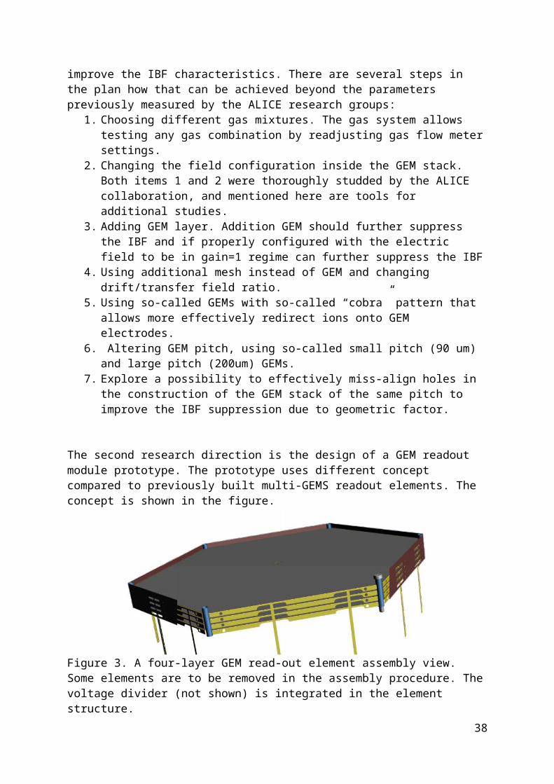
The second research direction is the design of a GEM readout module prototype. The prototype uses different concept compared to previously built multi-GEMS readout elements. The concept is shown in the figure.
Figure 3. A four-layer GEM read-out element assembly view. Some elements are to be removed in the assembly procedure. The voltage divider (not shown) is integrated in the element structure.The readout element is a standalone module, which has several crucial advantages:
1. Almost frameless design (approximately 600um between holes of adjacent modules) allows reducing inactive areas in the detector to a percent level. Residual areas that never fully shadow one single pad would result in a signal reduction rather than in a signal loss. Thus, this design, then proven to work, can be considered virtually a “no dead area” design.
2. Geometry of the GEM elements can be tailored to fit the entire fiducial area. 3. Loss of a single element has small impact on the TPC performance. 4. Each element is build out of approximately 100cm2 GEMs. Such GEMs can be
produced in large quantities at lower cost compared to larger GEMs of the equivalent area.
5. Uniformity of small GEMs is typically better than that of the large GEMs due to less demanding tolerance during the manufacturing stage.
6. Small size of the element may, in principle, allow to (miss-)align holes in different GEM layers for better IBF suppression.
7. Production, and more importantly, testing of GEM elements can be effectively done in parallel by several groups to keep up on the scheduler and to ensure the highest quality of the final detector.
8. Since the element is assembled in its final configuration already at the testing stage it can be fully calibrated before being mounted onto TPC.
9. Low cost of individual element allows pre-selecting the best elements to be used in the experiment and keeping the rest as a contingency.
10. Such element better suites to be used in future HBD-like detectors, there GEMs need to be coated with CsI. Pre-tested and coated element can be installed into its final position avoiding intermediate assembly required in a layer-by-layer procedure.
28
EquipmentThe group at the Weizmann Institute possesses a fully equipped clean room with the area of ~50 m2 shown in Figure 10.
Figure 4. The gaseous detector laboratory at the Weizmann Institute. The numbers on the photograph corresponds to the numbers in the text.
The clean room has the following equipment:
1. Rack with the NIM crates and various logical and service modules, the oscilloscope.2. Laminar Flow Table (LFT) for GEM assembly.3. Olympus BXFM optical system for visual inspection of the GEM foils and GEM
stacks. (This system is not visible in the photo in Figure 10 at location 3)4. CAEN mainframe with 12 channels HV module up to 5 kV. The system is expandable
to 60 HV channels.5. Glassman HV power supply for up to 40 kV.6. Fully automated, computer controlled gas flow system capable of mixing up to 4
different gases with the precision of 2%. The system has three gas flow lines which can be operated independently. The system integrates flow, pressure, humidity and oxygen content control devices.
7. Test cells for micro-pattern gaseous detector testing and gas studies:a. For 10 cm × 10 cm size detectors with 30 cm gas drift volume;b. For 20 cm × 30 cm size detectors without drift volume;c. Cells are connected to the turbo-pump based gas evacuation system;d. Cells are equipped with ionization source, MINI-X X-ray tube, and the UV-
laser system for gas ionization;e. Cells are connected to 10ch and 3ch floating picoampermeter system for
measuring currents in the micropatern detector layers.8. Data acquisition system for 512 channels, expandable to up to 4096 readout channels.9. Alternative DAQ with smaller number of channels.10. Standard laboratory equipment.
The cleanness of the air in the room outside the LFT working volume corresponds to Class ISO-8 clean room standards for particles less than 1 μm and exceeds that for larger particles. The cleanness of the room can be elevated; however, the detectors are normally not exposed to the room air outside the LFT volume. The clean room is considered as the main working place for the project. Additional rooms can be provided by the Institute infrastructure, if required. The resources which are available at the Weizmann Institute of Science and which will be used in order to perform the efforts for this project are listed below:
29

Instrumentation design unit. Machine shops. Electronic shop. Electronics & Data Acquisition unit. Instrument Control, Algorithms & Numerical Simulations unit.
The Institute Campus is situated near the Itzhak Rabin Scientific Park area, where many high-tech and research companies are located. Many can also be reached routinely if needed.
Yale University:
3-Coordinate GEMIn the coming period we will submit a paper on the final analysis.
Hybrid Gain Structure for TPC readoutWe expect to have fully functional MMG with resistive layers and continue to characterize their behavior.
Multi-element stacked gate grid.We will develop the switching circuit and continue investigation of the extended gating grid concept.
What are critical issues?
Brookhaven National Lab:
Our first priority will be to complete the analysis of the test beam data and to publish the final results. We have already gotten off to a good start and anticipate that this will take a few months to finish. In parallel, we are planning to start the IBF measurement at Stony Brook by the beginning of June and have already initiated testing two existing chevron patterns in the lab with our colleagues at FIT. Another important item that we want to start to consider over the next funding cycle is the choice of the TPC detector gas. There are many issues to consider when making this choice such as diffusion, IBF, and matching the drift velocity to the readout electronics, so we anticipate that a final decision will not be made in the near future, however it will be necessary to start to characterize a narrow list of potential candidate gases. Other than ensuring we make progress on these fronts, it is critical for us to complete the new designs of the chevron patterns that we started several months ago, so that we can move on to getting the corresponding boards fabricated and tested. One important concern that we have about this comes from previous experience that the quality of the board fabrication depends very strongly on the PCB shop we choose to make the board. For instance, we’ve had boards produced in the past where the PCB shop was not able to match the point resolution specified in the design. This issue could potentially pose significant delay as far as procuring good quality boards. However, having reached out to another group who has dealt with such issues, we have identified a particular PCB shop who we believe has the ability to produce the high quality boards we are looking for. Finally, identifying electronics suitable for the TPC readout is still an ongoing project, and at this point we are leaning towards using a version of the SAMPA chip used at STAR.
30
Florida Institute of Technology:
The most critical issue specifically for Florida Tech is the continued availability of post-doc Aiwu Zhang throughout construction and testing of the second EIC FT detector prototype, for which funding was initiated following the June 2015 review. The significant progress described in the “What was achieved?” section above, in particular getting publications out and designing the next FT detector prototype, is to a very large extent due to Aiwu’s comprehensive work on the project. He has been simultaneously filling the roles of physicist (data taking and analysis, publication), mechanical engineer (CAD design and FE analysis), and PCB designer (Altium board design) on the project. Due to his involvement on all fronts of the development process, Aiwu’s continued work is absolutely critical for completing the project in 2017. Without him, the EIC R&D effort on the second FT detector prototype at Florida Tech would die instantly. Due to the low overhead rates at Florida Tech, his employment is also a very cost-effective investment for the consortium. Consequently, we request that funding be provided to renew his position for another year in FY17 so that he can see the design, production, and performance testing of the previously funded FT prototype through to the publication of the performance results.
On the technical side, most PCB factories are apparently not able to produce zigzag strips on flexible PCB due to the fact that trace width and space are less than 3 mils in our design. The CERN workshop claims that they can do it, but we will have to validate the foil quality first.
INFN Trieste:
N/A
Stony Brook University:
The implementation of the ordered equipment and working mode for modifying the vacuum evaporator is the critical issue to finalize the evaporation of a large sized mirror.
University of Virginia:
a The production and tests of the new readout design on a smaller scale is a critical step before we can confidently go for the large size prototype. This is an area we would like to investigate in the next six months.
Weizmann Institute of Science:
N/A
Yale University:
Hybrid Gain Structure for TPC readoutCritical issues remain the same: develop methods for operating a TPC at high data rates while maintaining low ion feedback, good energy resolution and robust operation (low discharge rate).
31
Workforce
Include a list of the existing manpower and what approximate fraction each has spenton the project. If students and/or postdocs were funded through the R&D, please state where they were located and who supervised their work.
Brookhaven National Lab:
This work is being carried out by members of the BNL Physics Department. It includes one Senior Scientist (0.2 FTE), one Physics Associate (1.0 FTE), one Assistant Physicist (0.1 FTE) and one Technician (0.3 FTE). All personnel are paid by the BNL Physics Department.
Florida Institute of Technology:
Marcus Hohlmann, P.I., 0.25 FTE, not directly funded under this R&D program Aiwu Zhang, post-doc, 1 FTE, fully funded under this R&D program, located at
Florida Tech and supervised by M. Hohlmann Several undergraduates; unfunded.
INFN Trieste:
The proponents are part of the group from INFN-Sezione di Trieste and Trieste University presently active in the COMPASS experiment at CERN SPS. The group has two main lines of interest: hadron physics items and COMPASS data analysis and in hardware items, including R&D and detector construction; in particular, the Trieste group has designed COMPASS RICH-1, a large acceptance gaseous focusing RICH, has coordinated the project and built most of the counter components. Presently, the group has completed the construction for an upgrade of the RICH based on novel photon detectors by MPGD technologies. Therefore, the group competence in hardware is the field of RICHes and MPGDs. The group is formed by 12 units, including 5 staff ones; about half of the group is directly involved in the R&D proposed for the next three years:S. Dalla Torre (INFN, Staff)S. Dasgupta (Trieste University, PhD student)G. Hamar (INFN, postdoc)S. Levorato (INFN, Staff)F. Tessarotto (INFN, Staff)The contribution of technical personnel from INFN-Trieste is also foreseen according to needs.The manpower for this activity will be enriched by one more postdoc unit specifically enrolled for this R&D, working in Trieste under the supervision of S. Levorato and F. Tessarotto; financial support for this postdoc position is included in the requested founds.
Stony Brook University:
None of the labor at SBU is funded by EIC R&D. The workforce is listed below (in % FTE):K. Dehmelt Research Scientist 40%T. K. Hemmick Professor 10%N. Nguyen Undergraduate student 25%
32
University of Virginia:
None of the labor at UVa is funded by EIC R&D. The workforce is listed below (in % FTE):a N. Liyanage Professor 10%a K. Gnanvo Research Scientist 40%a V. Nelyubin Senior Research Scientist 5%a H. Nguyen Post-doctoral 5%a X. Bai Graduate Student 5%a R. Wang Graduate Student 5%
Weizmann Institute of Science:
The Heavy Ion research group at the Weizmann Institute includes the PI, one senior scientist working part time, 3 post-doctoral researchers, 2 PhD students, visiting scientist and part time graduate and undergraduate students. Personal focused on the detector research are: Prof. Alexander Milov part timeProf. Vladimir Peskov full timeDr. Lior Arazi part timePhD student part time
For short-term projects and critical research steps the manpower of the group can be focused on the detector studies. The group has long term well established relations with other research groups involved in the detector construction. The detector research group of Prof. Amos Breskin, the ATLAS High Energy group involved in the New Small Muon Wheel upgrade, the group of Dr. Shikma Bressler working on the ILC.
Yale University:
None of the labor at Yale is funded by EIC R&D. The workforce is listed below.R. Majka Senior Research Scientist and Scholar 10%N. Smirnov Research Scientist and Scholar 50%
Undergraduate Student 25%
External Funding
Describe what external funding was obtained, if any. The report must clarify what has been accomplished with the EIC R&D funds and what came as a contribution from potential collaborators.
Brookhaven National Lab:
There is currently no other external funding for this R&D effort
Florida Institute of Technology:
Florida Tech has no external grants in nuclear physics. There is a base grant in HEP for CMS that has some synergy with R&D work on large-area GEMs.
All work described above was accomplished with the EIC R&D funds.
INFN Trieste:
33

A request for financial support from INFN will be placed either starting in year 2017 or in year 2018, according to the indications of the INFN management and the general consolidation of the EIC project.
Stony Brook University:
There is no other external funding for this R&D effort.
University of Virginia:
a UVa has DOE basic research grant from Medium Energy Physics. The R&D work on Cr-GEM is funded with the research grant.
a The group also has DOE grants through JLab for the construction of the SBS GEM trackers.
Weizmann Institute of Science:
?
Yale University:
None
34
Budget Request for new EIC R&D funds.
Brookhaven National Lab:
We anticipate the following funding request for the next round of EIC R&D funding in FY17.
1. Expendable materials and supplies for gas detector lab - $10K 2. Travel - $5K 3. Design and materials for new chevron readout patterns - $10K 4. Parts and materials for investigation of GEM/Micromegas operation - $10K 5. New optics for VUV spectrometer - $10K
Total without overhead - $45K Total with overhead - $67.5K
Florida Institute of Technology:
The budget requested by Florida Tech for FY17 is listed in the following table. All amounts are fully loaded with fringe and overhead.
Forward tracking: large-area GEM with zigzag strip readoutPersonnel (post-doc, Aiwu Zhang)
$100k 12 months, fully loaded
GEM readout foil $9k From CERNGEM assembly parts $6k Frames, O-ring, connectors, etc.Supplies & material $2k Gas, T/P monitor, etc.Travel $7k Beam test(s); conference, consortium
meetingsTotal $124k
INFN Trieste:
The founding request for this R&D activity is presented in table 1, where the bare requests are listed and also the overhead is included assuming the typical INFN rate of 20%. The request includes 3 main chapters:
the financial support for a postdoc fully dedicated to the project: the contribution of a dedicated personnel unit will offer a crucial boost to the R&D program; 33000 $ corresponds to one-year postdoc salary in Italy;
traveling resources, mainly to have the possibility of closer interaction with the whole RD6 Consortium and to follow the evolution of the EIC project: 3 trips to US per year require about 9000 $; a minor support is requested for material procurement, to interact with the producers when non-standard components are needed and for the construction of specific detector elements that must be produced at CERN: this needs is estimated to be 3000 $ per year;
Consumables have to cover prototype components and prototype operation costs; the needs for the first year are already well defined and are listed in the following, while the request for the following years indicate a reasonable envelop and the details will be spelt out year by year.
Consumables for FY2017 include: Material and fabrication of novel substrate THGEMs: 6000 $;
35

Mechanics and equipment (connectors, gas connections, mechanical frames) to test the prototypes forming 2 dedicated chambers: 4000 $;
2 PCB for MMs with miniaturized pad-size: 4000 $; Production of two bulk MMs with miniaturized pad-size: 5000 $; Mechanics and equipment (resistors, connectors, gas connections, mechanical frames)
to test the MM with miniaturized pad-size, 1 dedicated chamber: 5000 $; Gas bottles to operate the detectors: 3000 $; Miscellanea of small items: 3000 $.
No founding for equipment is requested because, thanks to the long tradition and activity in the field of MPGDs and RICHes, the home laboratory of the Trieste group has a rich general purpose equipment and specific tools and instrumentation dedicated to the development of gaseous detectors and photon detectors. In particular:
SRS read-out set-up with APV25 front-end chip and related DAQ system; Small- and large-size glove boxes; Gas mixing units with mass flowmeters; X-ray station (source: AMPTEK miniature X-ray tube) with the capability to
illuminate also large surfaces of the order of 0.25 m2; High purity nitrogen generator (O2 contamination below 15 ppm, rate: 5l/min); Clean room, 6 m^2 (overpressure, constant flow of filtered air); Reference table (60 * 50 cm^2); HV systems by Caen; HV control system for voltage regulation to compensate for temperature and pressure
variations, custom, home-made; A large set of fully floating pico-ampmeters, custom, home-made; Set-up for surface polishing including a large-size ultrasonic bath; UV light sources including a Continuous High Intensity Deuterium Lamp UV system
and a pulsed source Picoquant picosecond Pulser PDL 800B with 265 nm and 255 nm UV light sources.
total (k$) (k$) (k$) (k$)
year 2017 2018 2019item manpower (1 unit for the 3 years of the project duration) 33 33 33 99travelling (3 trips to US per year + trips for material procurement and construction) 12 12 12 36consumables (specific for each year, according to the project time-lines) 30 30 30 90total 75 75 75 225
total adding overhead (at 20% level) 90 90 90 270
requested founding
36
Table 1 – Funding request.

Stony Brook University:
1. Purchase of IBF-GEM foils - $5k2. Expendable materials and supplies - $5k3. Support for beam test - $10k4. Travel - $5k
Total without overhead - $25kTotal with overhead - $40k
University of Virginia:
We anticipate the following funding request for the next round of EIC R&D funding in FY17. a Materials and Production of (U-V strips) readout board including the Zebra-
Panasonic adapter boards - $10K a Design and materials and production of GEM support frames - $4K a Expendable materials and supplies - $3K a Support for undergraduate student $5Ka Travel - $3K
Total without overhead - $25K
Weizmann Institute of Science:
GEM foils. Since currently the producer of GEMs is CERN, the cost of a single framed foil costs approximately $450. A non-standard GEM costs $600-$700 depending on design. Additional expense may include tooling ($300) and design work ($300). Depending on the research we would ask $10,000 to be spent on design and production of GEMs.
Another budget item is running the lab, which includes consumables such as gases, cleaning materials, IT service, small tooling and similar. Typical cost is $700 per month, $8400 per year.
Expense AmountDesign and production of GEM elements and tooling $10,000Operation of the detector lab (consumables, tooling, IT support, etc…) $8,400Total w/o overhead $18,400
Yale University: None (?)
37
Publications
Please provide a list of publications coming out of the R&D effort.
Brookhaven National Lab:
“A Study of a Mini-drift GEM Tracking Detector”, B. Azmoun et.al., submitted August, 2015 to the IEEE Transactions on Nuclear Science, accepted for publication in April 2016.
Requested an oral presentation at the IEEE NIS/MIC conference in Strasbourg, France in Fall 2016 on the TPC/Cherenkov hybrid detector.
Florida Institute of Technology:
A. Zhang and M. Hohlmann, “Accuracy of the geometric-mean method for determining spatial resolutions of tracking detectors in the presence of multiple Coulomb scattering,” submitted to JINST and posted on arXiv (1604.06130).
A. Zhang et al., “Study of non-linear response of a GEM read out with radial zigzag strips,” abstract submitted to the 2016 IEEE NSS/MIC conference in Strasbourg, France.
Reference
Carbon fiber mechanical properties, http://www.performance-composites.com/carbonfibre/mechanicalproperties_2.asp
INFN Trieste:
N/A
Stony Brook University:
1. “Performance of a Quintuple-GEM Based RICH Detector Prototype”, IEEE TRANSACTIONS ON NUCLEAR SCIENCE, VOL. 62, NO. 6, DECEMBER 2015.2. ”Performance of a Quintuple-GEM Based RICH Detector Prototype”, Nuclear Science Symposium Conference Record, 2015, IEEE
University of Virginia:
a K. Gnanvo, et al. “Large Size GEM for Super Bigbite Spectrometer (SBS) Polarimeter for Hall A 12 GeV program at JLab”, Nucl. Inst. and Meth. A782, 77-86 (2015). DOI: 10.1016/j.nima.2015.02.017
a K. Gnanvo et al., “Performance in Test Beam of a Large-area and Light-weight GEM detector with 2D Stereo-Angle (U-V) Strip Readout”, Nucl. Inst. and Meth. A808 (2016), pp. 83-92. DOI: 10.1016/j.nima.2015.11.071.
Weizmann Institute of Science:
N/A
Yale University:
A paper on the results to date has been submitted to NIM and is available at: http://arxiv.org/abs/1603.08473Combined Budget Request
38
Institute Total Request (k$)BNL 67.5Florida Tech 124INFN 90Stony Brook 40UVa 25WIS 18.4Yale ?SUM 364.5
39