Embed Size (px)
Citation preview
xE50-433/868 RF Module User Guide 1VV0300905 Rev.13 – 2015-07-28

xE50-433/868 RF Module User Guide 1VV0300905 Rev.13 – 2015-07-28
Reproduction forbidden without written authorizatio n from Telit Communications S.p.A. - All Rights Reserved. Page 2 of 50
APPLICABILITY TABLE
PRODUCT
LE50-433
LE50-868
NE50-868
NE50-433
ME50-868
xE50-433/868 RF Module User Guide 1VV0300905 Rev.13 – 2015-07-28
Reproduction forbidden without written authorizatio n from Telit Communications S.p.A. - All Rights Reserved. Page 3 of 50
SPECIFICATIONS SUBJECT TO CHANGE WITHOUT NOTICE
Notice While reasonable efforts have been made to assure the accuracy of this document, Telit assumes no liability resulting from any inaccuracies or omissions in this document, or from use of the information obtained herein. The information in this document has been carefully checked and is believed to be entirely reliable. However, no responsibility is assumed for inaccuracies or omissions. Telit reserves the right to make changes to any products described herein and reserves the right to revise this document and to make changes from time to time in content hereof with no obligation to notify any person of revisions or changes. Telit does not assume any liability arising out of the application or use of any product, software, or circuit described herein; neither does it convey license under its patent rights or the rights of others. It is possible that this publication may contain references to, or information about Telit products (machines and programs), programming, or services that are not announced in your country. Such references or information must not be construed to mean that Telit intends to announce such Telit products, programming, or services in your country.
Copyrights This instruction manual and the Telit products described in this instruction manual may be, include or describe copyrighted Telit material, such as computer programs stored in semiconductor memories or other media. Laws in the Italy and other countries preserve for Telit and its licensors certain exclusive rights for copyrighted material, including the exclusive right to copy, reproduce in any form, distribute and make derivative works of the copyrighted material. Accordingly, any copyrighted material of Telit and its licensors contained herein or in the Telit products described in this instruction manual may not be copied, reproduced, distributed, merged or modified in any manner without the express written permission of Telit. Furthermore, the purchase of Telit products shall not be deemed to grant either directly or by implication, estoppel, or otherwise, any license under the copyrights, patents or patent applications of Telit, as arises by operation of law in the sale of a product.
Computer Software Copyrights The Telit and 3rd Party supplied Software (SW) products described in this instruction manual may include copyrighted Telit and other 3rd Party supplied computer programs stored in semiconductor memories or other media. Laws in the Italy and other countries preserve for Telit and other 3rd Party supplied SW certain exclusive rights for copyrighted computer programs, including the exclusive right to copy or reproduce in any form the copyrighted computer program. Accordingly, any copyrighted Telit or other 3rd Party supplied SW computer programs contained in the Telit products described in this instruction manual may not be copied (reverse engineered) or reproduced in any manner without the express written permission of Telit or the 3rd Party SW supplier. Furthermore, the purchase of Telit products shall not be deemed to grant either directly or by implication, estoppel, or otherwise, any license under the copyrights, patents or patent applications of Telit or other 3rd Party supplied SW, except for the normal non-exclusive, royalty free license to use that arises by operation of law in the sale of a product.

xE50-433/868 RF Module User Guide 1VV0300905 Rev.13 – 2015-07-28
Reproduction forbidden without written authorizatio n from Telit Communications S.p.A. - All Rights Reserved. Page 4 of 50
Usage and Disclosure Restrictions
License Agreements The software described in this document is the property of Telit and its licensors. It is furnished by express license agreement only and may be used only in accordance with the terms of such an agreement.
Copyrighted Materials Software and documentation are copyrighted materials. Making unauthorized copies is prohibited by law. No part of the software or documentation may be reproduced, transmitted, transcribed, stored in a retrieval system, or translated into any language or computer language, in any form or by any means, without prior written permission of Telit
High Risk Materials Components, units, or third-party products used in the product described herein are NOT fault-tolerant and are NOT designed, manufactured, or intended for use as on-line control equipment in the following hazardous environments requiring fail-safe controls: the operation of Nuclear Facilities, Aircraft Navigation or Aircraft Communication Systems, Air Traffic Control, Life Support, or Weapons Systems (High Risk Activities"). Telit and its supplier(s) specifically disclaim any expressed or implied warranty of fitness for such High Risk Activities.
Trademarks TELIT and the Stylized T Logo are registered in Trademark Office. All other product or service names are the property of their respective owners.
Copyright © Telit Communications S.p.A. 2011.

xE50-433/868 RF Module User Guide 1VV0300905 Rev.13 – 2015-07-28
Reproduction forbidden without written authorizatio n from Telit Communications S.p.A. - All Rights Reserved. Page 5 of 50
Contents
1. Introduction ................................................. 7
1.1. Scope ............................................. ........ 7
1.2. Audience .......................................... ........ 7
1.3. Contact Information, Support ...................... ........ 7
1.4. Document Organization ............................. ........ 8
1.5. Text Conventions .................................. ........ 8
1.6. Related Documents ................................. ........ 9
2. Requirements ................................................ 10
2.1. General Requirements .............................. ....... 10
2.2. 433 MHz band Requirements ......................... ....... 10
2.3. 868 MHz band Requirements ......................... ....... 12
2.4. Other Requirements ................................ ....... 14
2.5. Functional Requirements ........................... ....... 14
2.6. Software .......................................... ....... 14
2.7. Temperature Requirements .......................... ....... 14
3. General Characteristics ..................................... 15
3.1. Mechanical Characteristics ........................ ....... 15
3.2. Mechanical dimensions ............................. ....... 16
3.3. Recommended Land pattern .......................... ....... 16
3.4. DC Characteristics ................................ ....... 17
3.5. LE50-433 Functional Characteristics ............... ....... 18
3.6. LE50-868 Functional Characteristics ............... ....... 20
3.7. NE50-433 Functional Characteristics ............... ....... 23
3.8. NE50-868 Functional Characteristics ............... ....... 25
3.9. ME50-868 Functional Characteristics ............... ....... 26
3.10. Digital Characteristic ............................ ..... 27
3.11. Absolute Maximum Ratings .......................... ..... 27
3.12. Ordering Information .............................. ..... 28
4. Technical Description ....................................... 30
4.1. Module Top View (cover side) ...................... ....... 30
4.2. Pin-out of the module LE50-433 and LE50-868 ....... ....... 31
xE50-433/868 RF Module User Guide 1VV0300905 Rev.13 – 2015-07-28
Reproduction forbidden without written authorizatio n from Telit Communications S.p.A. - All Rights Reserved. Page 6 of 50
4.3. Pin-out of the module NE50-433 and NE50-868 ....... ....... 32
4.4. Pin-out of the module ME50-868 .................... ....... 33
4.5. Pin-out of the DIP Module ......................... ....... 34
4.6. Description of the signals ........................ ....... 35
5. Process Information ......................................... 36
5.1. Delivery .......................................... ....... 36
5.2. Storage ........................................... ....... 37
5.3. Moisture sensibility .............................. ....... 37
5.4. Additional Precautions ............................ ....... 37
5.5. Soldering pad pattern ............................. ....... 37
5.6. Solder paste ...................................... ....... 38
5.7. PCB pad design .................................... ....... 39
5.8. PCB pad dimensions ................................ ....... 39
5.9. Placement ......................................... ....... 39
5.10. Soldering Profile (RoHS Process) .................. ..... 40
6. Board Mounting Recommendation ............................... 42
6.1. Electrical environment ............................ ....... 42
6.2. Power supply decoupling on xE50-433/868 module .... ....... 42
6.3. RF layout considerations .......................... ....... 43
6.4. Antenna connections on printed circuit boards ..... ....... 44
6.5. xE50-433/868 Interfacing .......................... ....... 45
7. Annexes ..................................................... 46
7.1. Examples of propagation attenuation ............... ....... 46
7.2. Declaration of conformity ......................... ....... 47
8. Safety Recommendations ...................................... 48
9. Glossary .................................................... 49
10. Document History ............................................ 50

xE50-433/868 RF Module User Guide 1VV0300905 Rev.13 – 2015-07-28
Reproduction forbidden without written authorizatio n from Telit Communications S.p.A. - All Rights Reserved. Page 7 of 50
1. Introduction
1.1. Scope Scope of this document is to present the features and the application of the Telit xE50-433/868 radio modules (LE50-433, LE50-868, NE50-433, NE50-868 and ME50-868).
1.2. Audience This document is intended for developers using Telit xE50-433/868 radio modules.
1.3. Contact Information, Support For general contact, technical support, to report documentation errors and to order manuals, contact Telit Technical Support Center (TTSC) at:
[email protected] [email protected] [email protected] [email protected]
Alternatively, use:
http://www.telit.com/en/products/technical-support-center/contact.php
For detailed information about where you can buy the Telit modules or for recommendations on accessories and components visit:
http://www.telit.com
To register for product news and announcements or for product questions contact Telit Technical Support Center (TTSC).
Our aim is to make this guide as helpful as possible. Keep us informed of your comments and suggestions for improvements.
Telit appreciates feedback from the users of our information.
xE50-433/868 RF Module User Guide 1VV0300905 Rev.13 – 2015-07-28
Reproduction forbidden without written authorizatio n from Telit Communications S.p.A. - All Rights Reserved. Page 8 of 50
1.4. Document Organization This document contains the following chapters
“Chapter 1: “Introduction” provides a scope for this document, target audience, contact and support information, and text conventions.
“Chapter 2: “Requirements” gives an overview of the limitations imposed by Reference standards.
“Chapter 3: “General Characteristics” describes in details the characteristics of the product.
“Chapter 4: “Technical Description” describes in details the signals and pin-out of the product.
“Chapter 5: “Process information” describes in details the delivery, storage, soldering and placement of the product.
“Chapter 6: “Board Mounting Recommendations” describes in details the interface and coupling of the product.
“Chapter 7: “Annexes” describes examples of propagation attenuation.
“Chapter 8: “Safety Recommendations” describes recommendation for proper usage.
“Chapter 9: “Glossary” shows acronyms used in the document.
“Chapter 10: “Document history” describes the revision history of the document.
1.5. Text Conventions
Danger – This information MUST be followed or catastrophic equipment failure or bodily injury may occur.
Caution or Warning – Alerts the user to important points about integrating the module, if these points are not followed, the module and end user equipment may fail or malfunction.
Tip or Information – Provides advice and suggestions that may be useful when integrating the module.
All dates are in ISO 8601 format, i.e. YYYY-MM-DD.
xE50-433/868 RF Module User Guide 1VV0300905 Rev.13 – 2015-07-28
Reproduction forbidden without written authorizatio n from Telit Communications S.p.A. - All Rights Reserved. Page 9 of 50
1.6. Related Documents
• [1] EN 300 220-2 v2.3.1, ETSI Standards for SRD , February 2010
• [2] ERC Rec 70-03, ERC Recommendation for SRD, June 2010
• [3] 2002/95/EC, Directive of the European Parliament and of the Council, 27 January 2003
• [4] SR Tool User Guide, 1vv0300899
• [5] 2006/771/EC, Harmonization of the radio spectrum for use by short-range devices
• [6] 2009/381/EC, Amending Decision 2006/771/EC on harmonization of the radio spectrum for use by short-range devices
• [7] Star Network Protocol Stack User Guide, 1vv0300873
• [8] Low Power Mesh Protocol Stack User Guide, 1vv0300944
• [9] Wireless M-Bus Part4+Part5 ModeR2 User Guide 1vv0300828
• [10] Wireless M-Bus Part 5 Mode Q User Guide 1vv0300935
• [11] EN 13757-4 : 2013 Wireless M-Bus
• [12] Telit_Wireless_M-bus_2013_Part4_User_Guide 1vv0300953
xE50-433/868 RF Module User Guide 1VV0300905 Rev.13 – 2015-07-28
Reproduction forbidden without written authorizatio n from Telit Communications S.p.A. - All Rights Reserved. Page 10 of 50
2. Requirements
2.1. General Requirements The LE50-433, LE50-868, NE50-868 and ME50-868 (or simply xE50-433/868) modules are multi-band radio boards, delivering up to 25 mW in the 868 MHz ISM band (unlicensed frequency band).
They are delivered with preloaded protocol stacks:
• LE50-433 and LE50-868: “Star Network” Protocol stack
• NE50-433 and NE50-868: “Low Power Mesh” Protocol stack
• ME50-868: “Wireless M-Bus Part4+Part5 ModeR2” Protocol stack, “Wireless M-Bus Part 5 Mode Q” Protocol stack and “Wireless M-Bus Part4:2013 Protocol stack.
LE50-433, LE50-868, NE50-433, NE50-868 and ME50-868 are pin-to-pin compatible with LE, NE and ME modules working at different frequencies.
LE50-433, LE50-868, NE50-433, NE50-868 and ME50-868 are also pin-to-pin compatible with Telit ZE Family (ZigBee PRO stack).
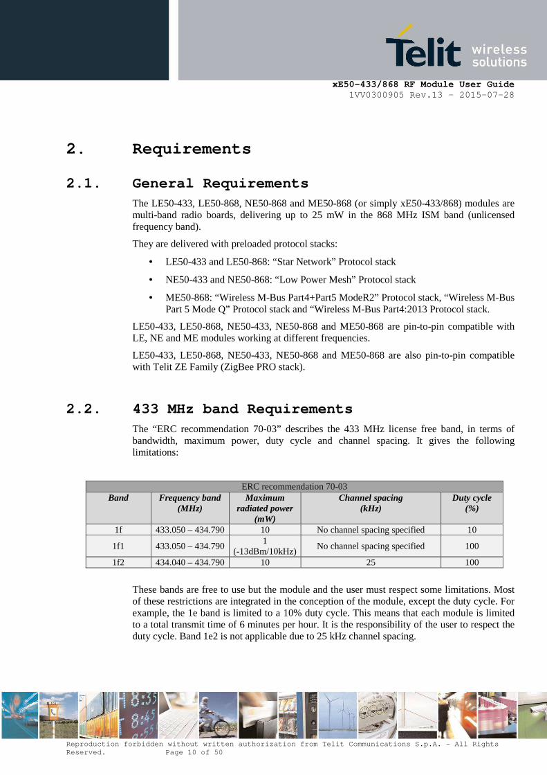
2.2. 433 MHz band Requirements The “ERC recommendation 70-03” describes the 433 MHz license free band, in terms of bandwidth, maximum power, duty cycle and channel spacing. It gives the following limitations:
ERC recommendation 70-03 Band Frequency band
(MHz) Maximum
radiated power (mW)
Channel spacing (kHz)
Duty cycle (%)
1f 433.050 – 434.790 10 No channel spacing specified 10
1f1 433.050 – 434.790 1
(-13dBm/10kHz) No channel spacing specified 100
1f2 434.040 – 434.790 10 25 100
These bands are free to use but the module and the user must respect some limitations. Most of these restrictions are integrated in the conception of the module, except the duty cycle. For example, the 1e band is limited to a 10% duty cycle. This means that each module is limited to a total transmit time of 6 minutes per hour. It is the responsibility of the user to respect the duty cycle. Band 1e2 is not applicable due to 25 kHz channel spacing.
xE50-433/868 RF Module User Guide 1VV0300905 Rev.13 – 2015-07-28
Reproduction forbidden without written authorizatio n from Telit Communications S.p.A. - All Rights Reserved. Page 11 of 50
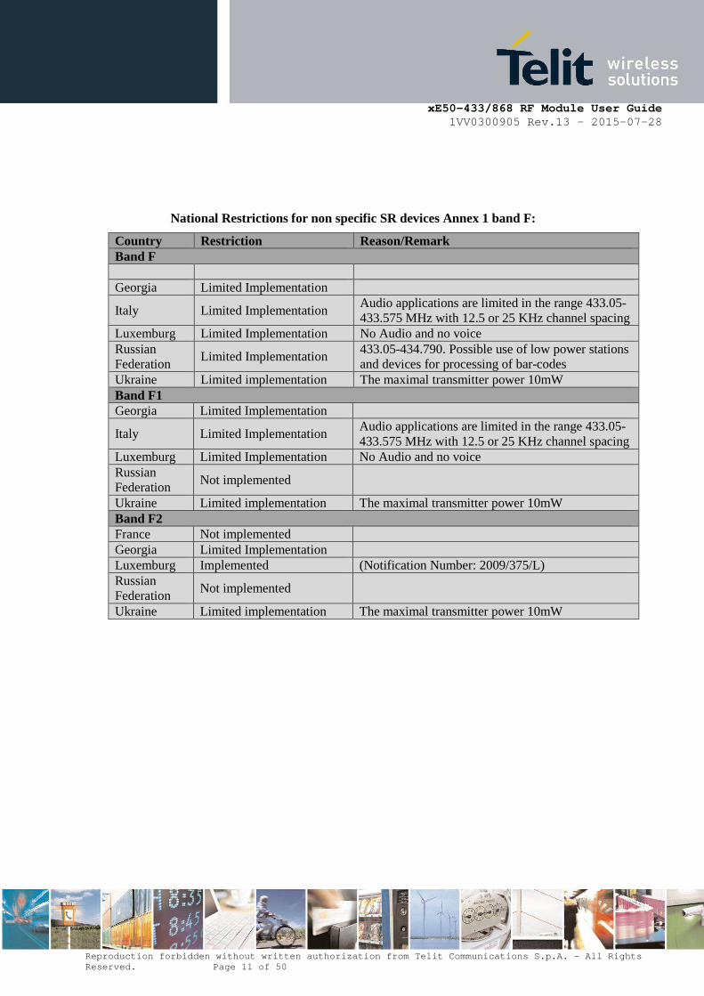
National Restrictions for non specific SR devices Annex 1 band F:
Country Restriction Reason/Remark Band F Georgia Limited Implementation
Italy Limited Implementation Audio applications are limited in the range 433.05-433.575 MHz with 12.5 or 25 KHz channel spacing
Luxemburg Limited Implementation No Audio and no voice Russian Federation
Limited Implementation 433.05-434.790. Possible use of low power stations and devices for processing of bar-codes
Ukraine Limited implementation The maximal transmitter power 10mW Band F1 Georgia Limited Implementation
Italy Limited Implementation Audio applications are limited in the range 433.05-433.575 MHz with 12.5 or 25 KHz channel spacing
Luxemburg Limited Implementation No Audio and no voice Russian Federation
Not implemented
Ukraine Limited implementation The maximal transmitter power 10mW Band F2 France Not implemented Georgia Limited Implementation Luxemburg Implemented (Notification Number: 2009/375/L) Russian Federation
Not implemented
Ukraine Limited implementation The maximal transmitter power 10mW
xE50-433/868 RF Module User Guide 1VV0300905 Rev.13 – 2015-07-28
Reproduction forbidden without written authorizatio n from Telit Communications S.p.A. - All Rights Reserved. Page 12 of 50
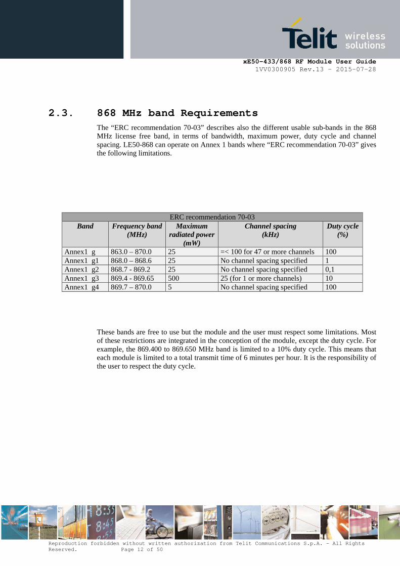
2.3. 868 MHz band Requirements The “ERC recommendation 70-03” describes also the different usable sub-bands in the 868 MHz license free band, in terms of bandwidth, maximum power, duty cycle and channel spacing. LE50-868 can operate on Annex 1 bands where “ERC recommendation 70-03” gives the following limitations.
ERC recommendation 70-03 Band Frequency band
(MHz) Maximum
radiated power (mW)
Channel spacing (kHz)
Duty cycle (%)
Annex1 g 863.0 – 870.0 25 =< 100 for 47 or more channels 100 Annex1 g1 868.0 – 868.6 25 No channel spacing specified 1 Annex1 g2 868.7 - 869.2 25 No channel spacing specified 0,1 Annex1 g3 869.4 - 869.65 500 25 (for 1 or more channels) 10 Annex1 g4 869.7 – 870.0 5 No channel spacing specified 100
These bands are free to use but the module and the user must respect some limitations. Most of these restrictions are integrated in the conception of the module, except the duty cycle. For example, the 869.400 to 869.650 MHz band is limited to a 10% duty cycle. This means that each module is limited to a total transmit time of 6 minutes per hour. It is the responsibility of the user to respect the duty cycle.
xE50-433/868 RF Module User Guide 1VV0300905 Rev.13 – 2015-07-28
Reproduction forbidden without written authorizatio n from Telit Communications S.p.A. - All Rights Reserved. Page 13 of 50
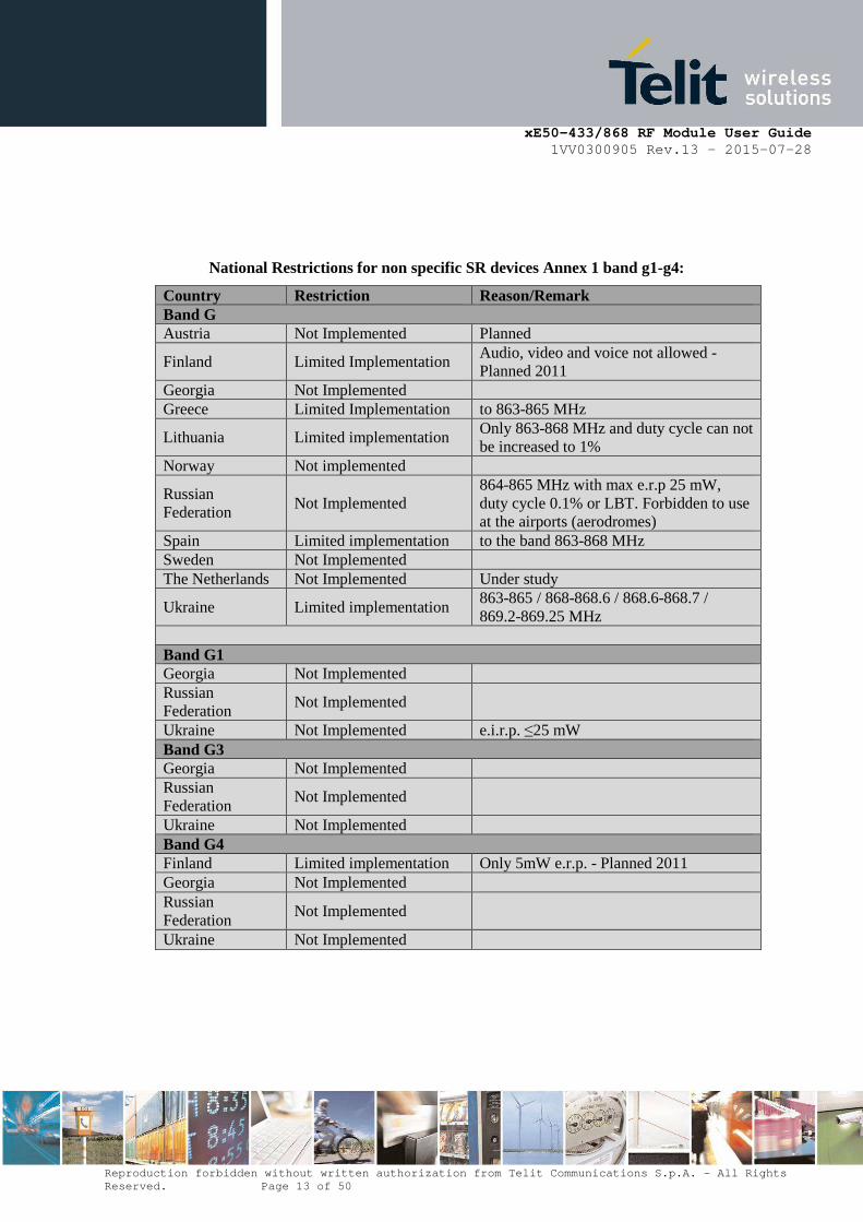
National Restrictions for non specific SR devices Annex 1 band g1-g4:
Country Restriction Reason/Remark Band G Austria Not Implemented Planned
Finland Limited Implementation Audio, video and voice not allowed - Planned 2011
Georgia Not Implemented Greece Limited Implementation to 863-865 MHz
Lithuania Limited implementation Only 863-868 MHz and duty cycle can not be increased to 1%
Norway Not implemented
Russian Federation
Not Implemented 864-865 MHz with max e.r.p 25 mW, duty cycle 0.1% or LBT. Forbidden to use at the airports (aerodromes)
Spain Limited implementation to the band 863-868 MHz Sweden Not Implemented The Netherlands Not Implemented Under study
Ukraine Limited implementation 863-865 / 868-868.6 / 868.6-868.7 / 869.2-869.25 MHz
Band G1 Georgia Not Implemented Russian Federation
Not Implemented
Ukraine Not Implemented e.i.r.p. ≤25 mW Band G3 Georgia Not Implemented Russian Federation
Not Implemented
Ukraine Not Implemented Band G4 Finland Limited implementation Only 5mW e.r.p. - Planned 2011 Georgia Not Implemented
Russian Federation
Not Implemented
Ukraine Not Implemented

xE50-433/868 RF Module User Guide 1VV0300905 Rev.13 – 2015-07-28
Reproduction forbidden without written authorizatio n from Telit Communications S.p.A. - All Rights Reserved. Page 14 of 50
2.4. Other Requirements Furthermore, the module complies with the ETSI 300-220-2 v2.3.1 standards (specific for SRD) which main requirements are described in Appendix 1. ME50-868 also complies which EN 13757-4 standards (Wireless M-Bus Part4).
Finally, the module complies with the new European Directive 2002/95/EC concerning the Restrictive Usage of Hazardous Substances (RoHS).
2.5. Functional Requirements The xE50-433/868 module is a complete solution from serial interface to RF interface. The xE50-868 module has a digital part and a RF part. The radio link is a Half Duplex bi-directional link.
The digital part has the following functionalities: • Communication interface • I/O management • Micro controller with embedded Telit Software Stack
The RF part has the following functionalities: • Frequency synthesis • Front-end • Low noise reception • Power amplification • Packet handling
2.6. Software The xE50-433/868 module is provided pre-flashed with one of the available Telit in-house Protocol Stack.
Please refer to Protocol Stack User Guides [7], [8], [9], [10] or [12] for detailed information.
2.7. Temperature Requirements
Minimum Typical Maximum Unit Operating
Temperature - 40 25 + 85 °C
Relative humidity @ 25°C
20 75 %
Storage
Temperature - 40 25 + 85 °C
xE50-433/868 RF Module User Guide 1VV0300905 Rev.13 – 2015-07-28
Reproduction forbidden without written authorizatio n from Telit Communications S.p.A. - All Rights Reserved. Page 15 of 50
3. General Characteristics
3.1. Mechanical Characteristics
Size : Rectangular 25.8 x 15 mm
Height : 3 mm
Weight : 1.7 g
PCB thickness: 0.8 mm
Cover : • Dimensions : 21 x 14.2 x 2.2mm • Thickness : 200µm
Components : All SMD components, on one side of the PCB.
Connectors : The terminals allowing conveying I/O signals are LGA
Mounting : • SMD • LGA on the 4 external sides
Number of pins : 30

xE50-433/868 RF Module User Guide 1VV0300905 Rev.13 – 2015-07-28
Reproduction forbidden without written authorizatio n from Telit Communications S.p.A. - All Rights Reserved. Page 16 of 50
3.2. Mechanical dimensions
3.3. Recommended Land pattern

xE50-433/868 RF Module User Guide 1VV0300905 Rev.13 – 2015-07-28
Reproduction forbidden without written authorizatio n from Telit Communications S.p.A. - All Rights Reserved. Page 17 of 50
3.4. DC Characteristics
Characteristics xE50 Min. Typ. Max.
Power Supply (VDD):
+2.0V +3.3V +3.6V
Consumption
xE50-433 - Transmission @ 10mW: 33mA 38mA
xE50-868 - Transmission @ 25mW: 45mA 50mA
Reception : 26mA 30mA
Stand-by (32.768 khz On) : 1.5µA 3µA
Sleep (wake up on interruption) : <1µA 1µA
I/O low level : GND - 0.2x VDD
I/O high level : 0.8x VDD - VDD
xE50-433/868 RF Module User Guide 1VV0300905 Rev.13 – 2015-07-28
Reproduction forbidden without written authorizatio n from Telit Communications S.p.A. - All Rights Reserved. Page 18 of 50
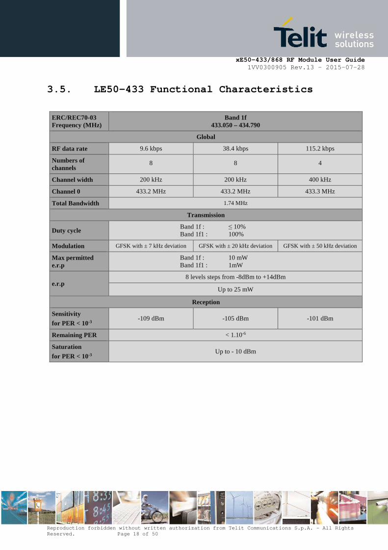
3.5. LE50-433 Functional Characteristics
ERC/REC70-03 Frequency (MHz)
Band 1f 433.050 – 434.790
Global
RF data rate 9.6 kbps 38.4 kbps 115.2 kbps
Numbers of channels
8 8 4
Channel width 200 kHz 200 kHz 400 kHz
Channel 0 433.2 MHz 433.2 MHz 433.3 MHz
Total Bandwidth 1.74 MHz
Transmission
Duty cycle Band 1f : ≤ 10% Band 1f1 : 100%
Modulation GFSK with ± 7 kHz deviation GFSK with ± 20 kHz deviation GFSK with ± 50 kHz deviation
Max permitted e.r.p
Band 1f : 10 mW Band 1f1 : 1mW
e.r.p 8 levels steps from -8dBm to +14dBm
Up to 25 mW
Reception
Sensitivity
for PER < 10-3 -109 dBm -105 dBm -101 dBm
Remaining PER < 1.10-6
Saturation
for PER < 10-3 Up to - 10 dBm

xE50-433/868 RF Module User Guide 1VV0300905 Rev.13 – 2015-07-28
Reproduction forbidden without written authorizatio n from Telit Communications S.p.A. - All Rights Reserved. Page 19 of 50
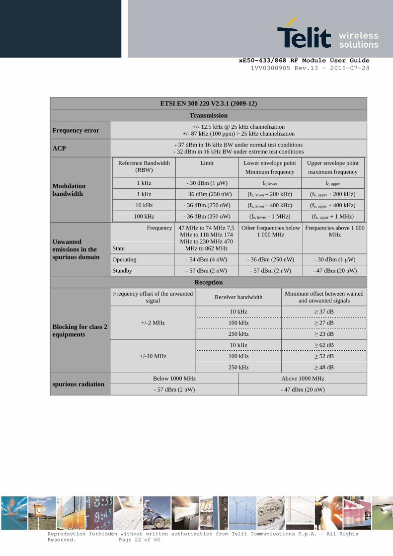
ETSI EN 300 220 V2.3.1 (2009-12)
Transmission
Frequency error +/- 12.5 kHz @ 25 kHz channelization +/- 87 kHz (100 ppm) > 25 kHz channelization
ACP - 37 dBm in 16 kHz BW under normal test conditions - 32 dBm in 16 kHz BW under extreme test conditions
Modulation bandwidth
Reference Bandwidth (RBW)
Limit Lower envelope point
Minimum frequency
Upper envelope point
maximum frequency
1 kHz - 30 dBm (1 µW) fe, lower fe, upper
1 kHz - 36 dBm (250 nW) (fe, lower – 200 kHz) (fe, upper + 200 kHz)
10 kHz - 36 dBm (250 nW) (fe, lower – 400 kHz) (fe, upper + 400 kHz)
100 kHz - 36 dBm (250 nW) (fe, lower – 1 MHz) (fe, upper + 1 MHz)
Unwanted emissions in the spurious domain
Frequency 47 MHz to 74 MHz 7,5 MHz to 118 MHz 174 MHz
to 230 MHz 470 MHz to 862 MHz
Other frequencies below 1 000 MHz
Frequencies above 1 000 MHz
State
Operating - 54 dBm (4 nW) - 36 dBm (250 nW) - 30 dBm (1 µW)
Standby - 57 dBm (2 nW) - 57 dBm (2 nW) - 47 dBm (20 nW)
Reception
Blocking for class 2 equipments
Frequency offset of the unwanted signal
Receiver bandwidth Minimum offset between wanted
and unwanted signals
+/-2 MHz
10 kHz ≥ 37 dB
100 kHz ≥ 27 dB
250 kHz ≥ 23 dB
+/-10 MHz
10 kHz ≥ 62 dB
100 kHz ≥ 52 dB
250 kHz ≥ 48 dB
spurious radiation Below 1000 MHz Above 1000 MHz
- 57 dBm (2 nW) - 47 dBm (20 nW)
xE50-433/868 RF Module User Guide 1VV0300905 Rev.13 – 2015-07-28
Reproduction forbidden without written authorizatio n from Telit Communications S.p.A. - All Rights Reserved. Page 20 of 50
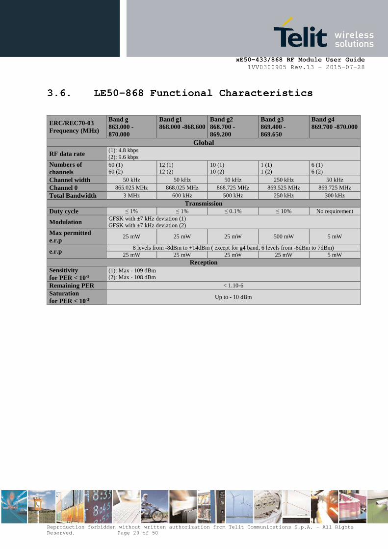
3.6. LE50-868 Functional Characteristics
ERC/REC70-03 Frequency (MHz)
Band g 863.000 -870.000
Band g1 868.000 -868.600
Band g2 868.700 -869.200
Band g3 869.400 -869.650
Band g4 869.700 -870.000
Global
RF data rate (1): 4.8 kbps (2): 9.6 kbps
Numbers of channels
60 (1) 60 (2)
12 (1) 12 (2)
10 (1) 10 (2)
1 (1) 1 (2)
6 (1) 6 (2)
Channel width 50 kHz 50 kHz 50 kHz 250 kHz 50 kHz Channel 0 865.025 MHz 868.025 MHz 868.725 MHz 869.525 MHz 869.725 MHz Total Bandwidth 3 MHz 600 kHz 500 kHz 250 kHz 300 kHz
Transmission Duty cycle ≤ 1% ≤ 1% ≤ 0.1% ≤ 10% No requirement
Modulation GFSK with ±7 kHz deviation (1) GFSK with ±7 kHz deviation (2)
Max permitted e.r.p
25 mW 25 mW 25 mW 500 mW 5 mW
e.r.p 8 levels from -8dBm to +14dBm ( except for g4 band, 6 levels from -8dBm to 7dBm)
25 mW 25 mW 25 mW 25 mW 5 mW Reception
Sensitivity for PER < 10-3
(1): Max - 109 dBm (2): Max - 108 dBm
Remaining PER < 1.10-6 Saturation for PER < 10-3
Up to - 10 dBm
xE50-433/868 RF Module User Guide 1VV0300905 Rev.13 – 2015-07-28
Reproduction forbidden without written authorizatio n from Telit Communications S.p.A. - All Rights Reserved. Page 21 of 50
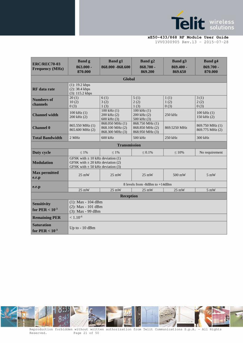
ERC/REC70-03 Frequency (MHz)
Band g
863.000 -870.000
Band g1
868.000 -868.600
Band g2
868.700 -869.200
Band g3
869.400 -869.650
Band g4
869.700 -870.000
Global
RF data rate (1): 19.2 kbps (2): 38.4 kbps (3): 115.2 kbps
Numbers of channels
20 (1) 10 (2) 0 (3)
6 (1) 3 (2) 1 (3)
5 (1) 2 (2) 1 (3)
1 (1) 1 (2) 0 (3)
3 (1) 2 (2) 0 (3)
Channel width 100 kHz (1) 200 kHz (2)
100 kHz (1) 200 kHz (2) 600 kHz (3)
100 kHz (1) 200 kHz (2) 500 kHz (3)
250 kHz 100 kHz (1) 150 kHz (2)
Channel 0 865.550 MHz (1) 865.600 MHz (2)
868.050 MHz (1) 868.100 MHz (2) 868.300 MHz (3)
868.750 MHz (1) 868.850 MHz (2) 868.950 MHz (3)
869.5250 MHz 869.750 MHz (1) 869.775 MHz (2)
Total Bandwidth 2 MHz 600 kHz 500 kHz 250 kHz 300 kHz
Transmission
Duty cycle ≤ 1% ≤ 1% ≤ 0.1% ≤ 10% No requirement
Modulation GFSK with ± 10 kHz deviation (1) GFSK with ± 20 kHz deviation (2) GFSK with ± 50 kHz deviation (3)
Max permitted e.r.p
25 mW 25 mW 25 mW 500 mW 5 mW
e.r.p 8 levels from -8dBm to +14dBm
25 mW 25 mW 25 mW 25 mW 5 mW
Reception
Sensitivity
for PER < 10-3
(1): Max - 104 dBm (2): Max - 101 dBm (3): Max - 99 dBm
Remaining PER < 1.10-6
Saturation
for PER < 10-3 Up to - 10 dBm
xE50-433/868 RF Module User Guide 1VV0300905 Rev.13 – 2015-07-28
Reproduction forbidden without written authorizatio n from Telit Communications S.p.A. - All Rights Reserved. Page 22 of 50
ETSI EN 300 220 V2.3.1 (2009-12)
Transmission
Frequency error +/- 12.5 kHz @ 25 kHz channelization +/- 87 kHz (100 ppm) > 25 kHz channelization
ACP - 37 dBm in 16 kHz BW under normal test conditions - 32 dBm in 16 kHz BW under extreme test conditions
Modulation bandwidth
Reference Bandwidth (RBW)
Limit Lower envelope point
Minimum frequency
Upper envelope point
maximum frequency
1 kHz - 30 dBm (1 µW) fe, lower fe, upper
1 kHz 36 dBm (250 nW) (fe, lower – 200 kHz) (fe, upper + 200 kHz)
10 kHz - 36 dBm (250 nW) (fe, lower – 400 kHz) (fe, upper + 400 kHz)
100 kHz - 36 dBm (250 nW) (fe, lower – 1 MHz) (fe, upper + 1 MHz)
Unwanted emissions in the spurious domain
Frequency 47 MHz to 74 MHz 7,5 MHz to 118 MHz 174 MHz to 230 MHz 470
MHz to 862 MHz
Other frequencies below 1 000 MHz
Frequencies above 1 000 MHz
State
Operating - 54 dBm (4 nW) - 36 dBm (250 nW) - 30 dBm (1 µW)
Standby - 57 dBm (2 nW) - 57 dBm (2 nW) - 47 dBm (20 nW)
Reception
Blocking for class 2 equipments
Frequency offset of the unwanted signal
Receiver bandwidth Minimum offset between wanted
and unwanted signals
+/-2 MHz
10 kHz ≥ 37 dB
100 kHz ≥ 27 dB
250 kHz ≥ 23 dB
+/-10 MHz
10 kHz ≥ 62 dB
100 kHz ≥ 52 dB
250 kHz ≥ 48 dB
spurious radiation Below 1000 MHz Above 1000 MHz
- 57 dBm (2 nW) - 47 dBm (20 nW)
xE50-433/868 RF Module User Guide 1VV0300905 Rev.13 – 2015-07-28
Reproduction forbidden without written authorizatio n from Telit Communications S.p.A. - All Rights Reserved. Page 23 of 50
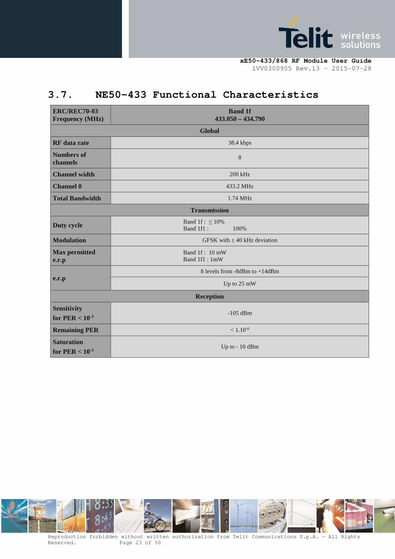
3.7. NE50-433 Functional Characteristics
ERC/REC70-03 Frequency (MHz)
Band 1f 433.050 – 434.790
Global
RF data rate 38.4 kbps
Numbers of channels
8
Channel width 200 kHz
Channel 0 433.2 MHz
Total Bandwidth 1.74 MHz
Transmission
Duty cycle Band 1f : ≤ 10% Band 1f1 : 100%
Modulation GFSK with ± 40 kHz deviation
Max permitted e.r.p
Band 1f : 10 mW Band 1f1 : 1mW
e.r.p 8 levels from -8dBm to +14dBm
Up to 25 mW
Reception
Sensitivity
for PER < 10-3 -105 dBm
Remaining PER < 1.10-6
Saturation
for PER < 10-3 Up to - 10 dBm

xE50-433/868 RF Module User Guide 1VV0300905 Rev.13 – 2015-07-28
Reproduction forbidden without written authorizatio n from Telit Communications S.p.A. - All Rights Reserved. Page 24 of 50
ETSI EN 300 220 V2.3.1 (2009-12)
Transmission
Frequency error +/- 12.5 kHz @ 25 kHz channelization +/- 87 kHz (100 ppm) > 25 kHz channelization
ACP - 37 dBm in 16 kHz BW under normal test conditions - 32 dBm in 16 kHz BW under extreme test conditions
Modulation bandwidth
Reference Bandwidth (RBW)
Limit Lower envelope point
Minimum frequency
Upper envelope point
maximum frequency
1 kHz - 30 dBm (1 µW) fe, lower fe, upper
1 kHz - 36 dBm (250 nW) (fe, lower – 200 kHz) (fe, upper + 200 kHz)
10 kHz - 36 dBm (250 nW) (fe, lower – 400 kHz) (fe, upper + 400 kHz)
100 kHz - 36 dBm (250 nW) (fe, lower – 1 MHz) (fe, upper + 1 MHz)
Unwanted emissions in the spurious domain
Frequency 47 MHz to 74 MHz 7,5 MHz to 118 MHz 174 MHz to 230 MHz 470
MHz to 862 MHz
Other frequencies below 1 000 MHz
Frequencies above 1 000 MHz
State
Operating - 54 dBm (4 nW) - 36 dBm (250 nW) - 30 dBm (1 µW)
Standby - 57 dBm (2 nW) - 57 dBm (2 nW) - 47 dBm (20 nW)
Reception
Blocking for class 2 equipments
Frequency offset of the unwanted signal
Receiver bandwidth Minimum offset between wanted
and unwanted signals
+/-2 MHz
10 kHz ≥ 37 dB
100 kHz ≥ 27 dB
250 kHz ≥ 23 dB
+/-10 MHz
10 kHz ≥ 62 dB
100 kHz ≥ 52 dB
250 kHz ≥ 48 dB
spurious radiation Below 1000 MHz Above 1000 MHz
- 57 dBm (2 nW) - 47 dBm (20 nW)
xE50-433/868 RF Module User Guide 1VV0300905 Rev.13 – 2015-07-28
Reproduction forbidden without written authorizatio n from Telit Communications S.p.A. - All Rights Reserved. Page 25 of 50
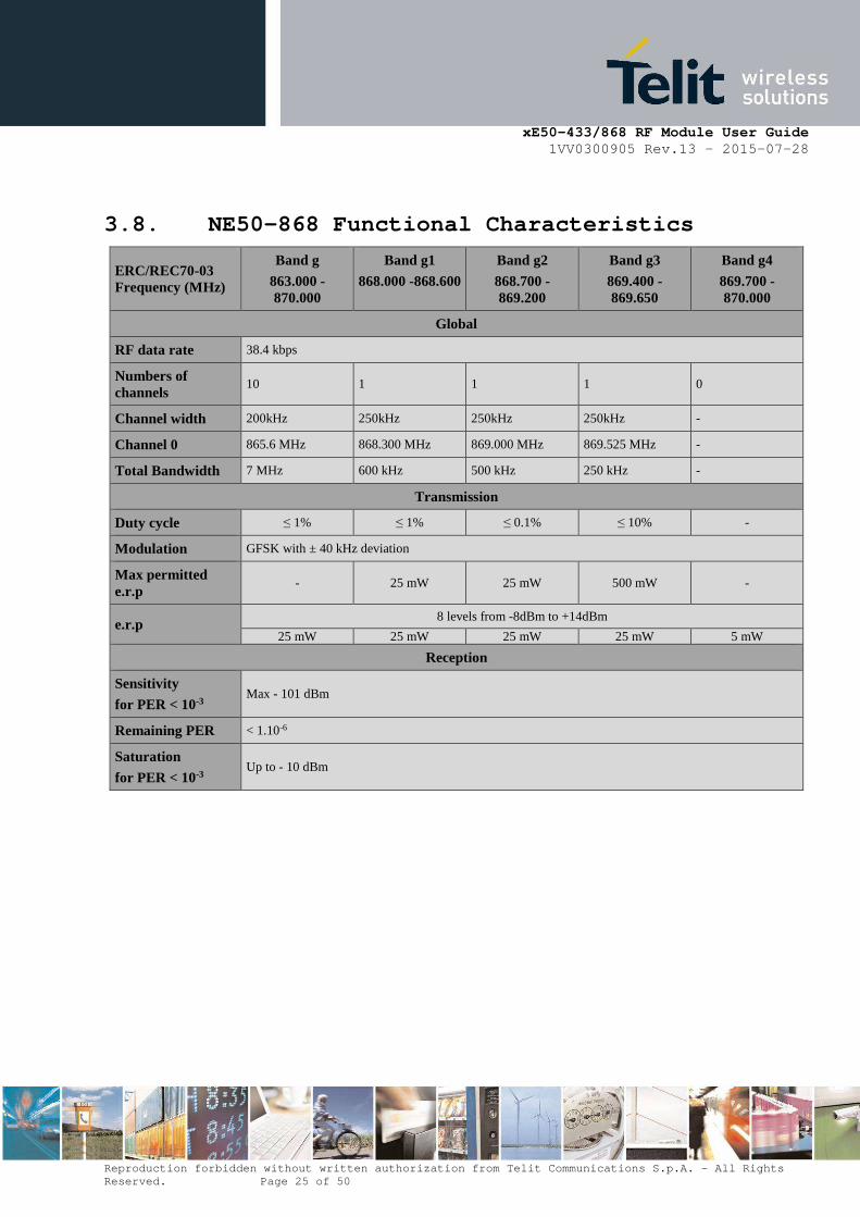
3.8. NE50-868 Functional Characteristics
ERC/REC70-03 Frequency (MHz)
Band g
863.000 -870.000
Band g1
868.000 -868.600
Band g2
868.700 -869.200
Band g3
869.400 -869.650
Band g4
869.700 -870.000
Global
RF data rate 38.4 kbps
Numbers of channels
10 1 1 1 0
Channel width 200kHz 250kHz 250kHz 250kHz -
Channel 0 865.6 MHz 868.300 MHz 869.000 MHz 869.525 MHz -
Total Bandwidth 7 MHz 600 kHz 500 kHz 250 kHz -
Transmission
Duty cycle ≤ 1% ≤ 1% ≤ 0.1% ≤ 10% -
Modulation GFSK with ± 40 kHz deviation
Max permitted e.r.p
- 25 mW 25 mW 500 mW -
e.r.p 8 levels from -8dBm to +14dBm
25 mW 25 mW 25 mW 25 mW 5 mW
Reception
Sensitivity
for PER < 10-3 Max - 101 dBm
Remaining PER < 1.10-6
Saturation
for PER < 10-3 Up to - 10 dBm

xE50-433/868 RF Module User Guide 1VV0300905 Rev.13 – 2015-07-28
Reproduction forbidden without written authorizatio n from Telit Communications S.p.A. - All Rights Reserved. Page 26 of 50
3.9. ME50-868 Functional Characteristics
NOTE: For Wireless Mbus functional characteristics (ME50-868 only) refer to [9] “Wireless M-Bus Part4+Part5 ModeR2 User Guide, to [10] “Wireless M-Bus Part 5 Mode Q User Guide 1vv0300935” and to [12] Telit_Wireless_M-bus_2013_Part4_User_Guide 1vv0300953
xE50-433/868 RF Module User Guide 1VV0300905 Rev.13 – 2015-07-28
Reproduction forbidden without written authorizatio n from Telit Communications S.p.A. - All Rights Reserved. Page 27 of 50
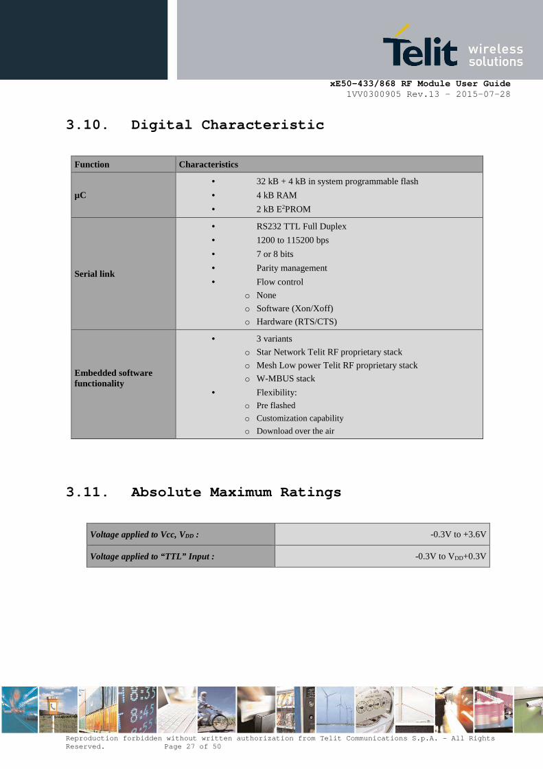
3.10. Digital Characteristic
Function Characteristics
µC
• 32 kB + 4 kB in system programmable flash
• 4 kB RAM
• 2 kB E2PROM
Serial link
• RS232 TTL Full Duplex
• 1200 to 115200 bps
• 7 or 8 bits
• Parity management
• Flow control
o None
o Software (Xon/Xoff)
o Hardware (RTS/CTS)
Embedded software functionality
• 3 variants
o Star Network Telit RF proprietary stack
o Mesh Low power Telit RF proprietary stack
o W-MBUS stack
• Flexibility:
o Pre flashed
o Customization capability
o Download over the air
3.11. Absolute Maximum Ratings
Voltage applied to Vcc, VDD : -0.3V to +3.6V
Voltage applied to “TTL” Input : -0.3V to VDD+0.3V
xE50-433/868 RF Module User Guide 1VV0300905 Rev.13 – 2015-07-28
Reproduction forbidden without written authorizatio n from Telit Communications S.p.A. - All Rights Reserved. Page 28 of 50
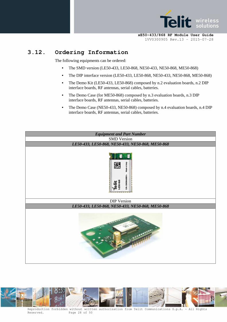
3.12. Ordering Information The following equipments can be ordered:
• The SMD version (LE50-433, LE50-868, NE50-433, NE50-868, ME50-868)
• The DIP interface version (LE50-433, LE50-868, NE50-433, NE50-868, ME50-868)
• The Demo Kit (LE50-433, LE50-868) composed by n.2 evaluation boards, n.2 DIP interface boards, RF antennas, serial cables, batteries.
• The Demo Case (for ME50-868) composed by n.3 evaluation boards, n.3 DIP interface boards, RF antennas, serial cables, batteries.
• The Demo Case (NE50-433, NE50-868) composed by n.4 evaluation boards, n.4 DIP interface boards, RF antennas, serial cables, batteries.
Equipment and Part Number SMD Version
LE50-433, LE50-868, NE50-433, NE50-868, ME50-868
DIP Version LE50-433, LE50-868, NE50-433, NE50-868, ME50-868

xE50-433/868 RF Module User Guide 1VV0300905 Rev.13 – 2015-07-28
Reproduction forbidden without written authorizatio n from Telit Communications S.p.A. - All Rights Reserved. Page 29 of 50
Demo Kit
D LE50 DemoKit
Demo Case
D NE50 DemoCase, D ME50 DemoCase
xE50-433/868 RF Module User Guide 1VV0300905 Rev.13 – 2015-07-28
Reproduction forbidden without written authorizatio n from Telit Communications S.p.A. - All Rights Reserved. Page 30 of 50
4. Technical Description
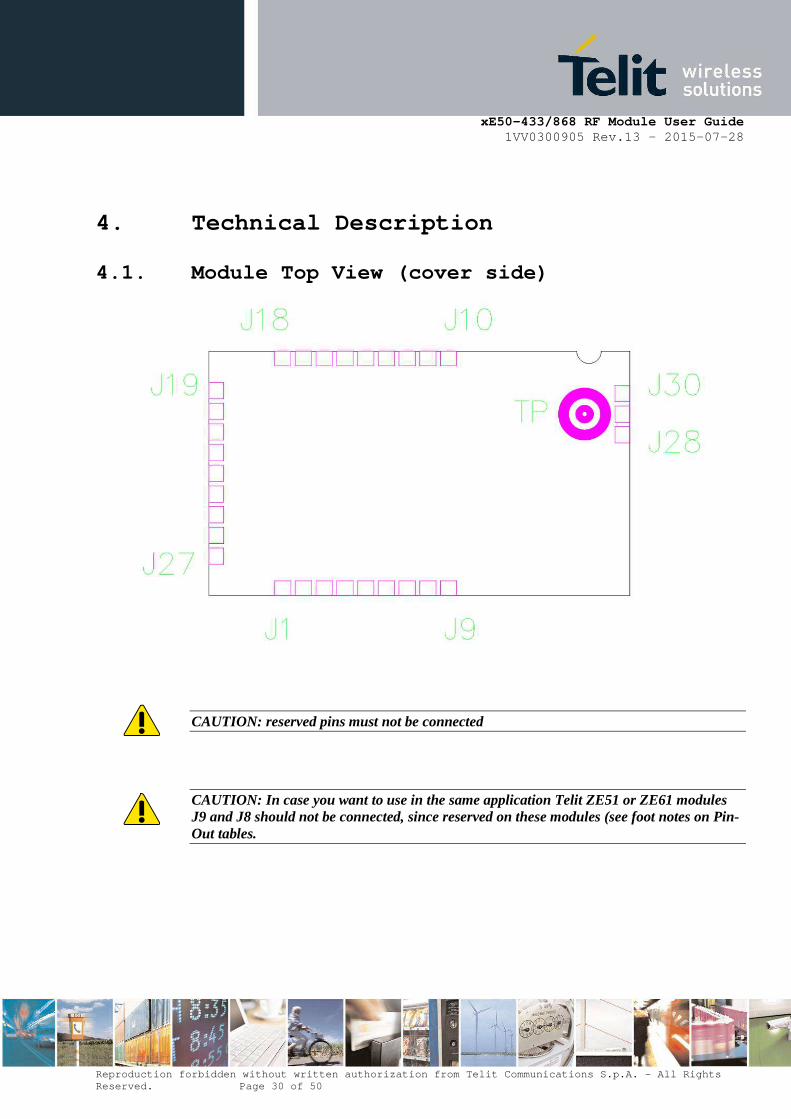
4.1. Module Top View (cover side)
CAUTION: reserved pins must not be connected
CAUTION: In case you want to use in the same application Telit ZE51 or ZE61 modules J9 and J8 should not be connected, since reserved on these modules (see foot notes on Pin-Out tables.

xE50-433/868 RF Module User Guide 1VV0300905 Rev.13 – 2015-07-28
Reproduction forbidden without written authorizatio n from Telit Communications S.p.A. - All Rights Reserved. Page 31 of 50
4.2. Pin-out of the module LE50-433 and LE50-868
Pin Pin name Pin type Signal level Function
J30 GND Gnd RF Ground connection for external antenna
J29 Ext_Antenna RF RF I/O connection to external antenna
J28 GND Gnd RF Ground connection for external antenna
J27 GND Gnd Ground
J26 GND Gnd Ground
J25 VDD Power Digital and Radio part power supply pin
J24 CTS I TTL Clear To Send
J23 RESET I TTL µC reset ( Active low with internal pull-up )
J22 RTS O TTL Request To Send
J21 RXD I TTL RxD UART – Serial Data Reception
J20 GND Gnd Ground
J19 TXD O TTL TxD UART – Serial Data Transmission
J18 STAND_BY I TTL Standby (Active high with internal pull-down: when set to 1 the module is put in stand-by)
J17 GND Gnd Ground
J16 PROG I TTL Signal for serial µC flashing ( Active high with internal pull-down )
J15 GND Gnd Ground
J14 PDI_DATA I/O TTL Program and Debug Interface DATA
J13 GND Gnd Ground
J12 GND Gnd Ground
J11 GND Gnd Ground
J10 PDI_CLK I TTL Program and Debug Interface CLOCK
J9 IO91 I/O TTL Digital I/O N°9 with interrupt
Status TX/RX O TTL See reference document [5] Star Network Protocol Stack User Guide
J8 IO8_AD_DA2 I/O TTL Digital I/O N°8 with interrupt
ACK TX O TTL See reference document [5] Star Network Protocol Stack User Guide
J7 IO7_A I/O TTL Digital I/O N°7 with interrupt
J6 IO6_A I/O analog ADC - Analog Input N°6 (Logic I/O capability)
J5 IO5_A I/O analog ADC - Analog Input N°5 (Logic I/O capability)
J4 IO4_A I/O analog ADC - Analog Input N°4 (Logic I/O capability)
J3 IO3_A I/O analog ADC - Analog Input N°3 (Logic I/O capability)
J2 IO2_P I/O TTL Logic I/O N°2 with interrupt
RX LED O TTL See reference document [5] Star Network Protocol Stack User Guide
J1 IO1_P I/O TTL Logic I/O N°1 with interrupt
TX LED O TTL See reference document [5] Star Network Protocol Stack User Guide
1, 2 In case you want to use in the same application Telit ZE51 or ZE61 modules J9 and J8 should not be connected, since reserved on these modules.

xE50-433/868 RF Module User Guide 1VV0300905 Rev.13 – 2015-07-28
Reproduction forbidden without written authorizatio n from Telit Communications S.p.A. - All Rights Reserved. Page 32 of 50
4.3. Pin-out of the module NE50-433 and NE50-868
Pin Pin name Pin type Signal level Function
J30 GND Gnd RF Ground connection for external antenna
J29 Ext_Antenna RF RF I/O connection to external antenna
J28 GND Gnd RF Ground connection for external antenna
J27 GND Gnd Ground
J26 GND Gnd Ground
J25 VDD Power Digital and Radio part power supply pin
J24 CTS I TTL Clear To Send
J23 RESET I TTL µC reset (Active low with internal pull-up )
J22 RTS O TTL Request To Send
J21 RXD I TTL RxD UART – Serial Data Reception
J20 GND Gnd Ground
J19 TXD O TTL TxD UART – Serial Data Transmission
J18 WAKEUP I TTL Wake-up (Active high with internal pull-down: when set to 1 the module is awakened)
J17 GND Gnd Ground
J16 PROG I TTL Signal for serial µC flashing ( Active high with internal pull-down )
J15 GND Gnd Ground
J14 PDI_DATA I/O TTL Program and Debug Interface DATA
J13 GND Gnd Ground
J12 GND Gnd Ground
J11 GND Gnd Ground
J10 PDI_CLK I TTL Program and Debug Interface CLOCK
J9 IO93 I/O TTL Digital I/O.
J8 IO8_AD_DA4
I/O analog Digital I/O. Analog Input and Interrupt Input capable. (Logic I/O capability)
J7 IO7_A I/O analog Digital I/O. Analog Input and Interrupt Input capable. (Logic I/O capability)
J6 IO6_A I/O analog Digital I/O. Analog Input and Interrupt Input capable. (Logic I/O capability)
J5 IO5_A I/O analog Digital I/O. Analog Input and Interrupt Input capable. (Logic I/O capability)
J4 IO4_A I/O analog Digital I/O. Analog Input and Interrupt Input capable. (Logic I/O capability)
J3 IO3_A I/O analog Digital I/O. Analog Input and Interrupt Input capable. (Logic I/O capability)
J2 STANDBY STATUS
O TTL Signal indicating stand-by status.
J1 ASSO O TTL ASSO - Signal indicating association status.
3, 4 In case you want to use in the same application Telit ZE51 or ZE61 modules J9 and J8 should not be connected, since reserved on these modules.
xE50-433/868 RF Module User Guide 1VV0300905 Rev.13 – 2015-07-28
Reproduction forbidden without written authorizatio n from Telit Communications S.p.A. - All Rights Reserved. Page 33 of 50
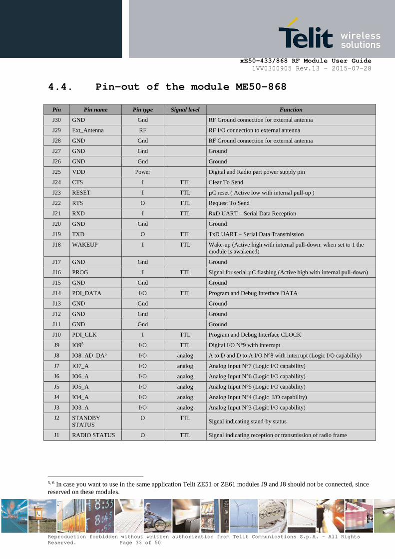
4.4. Pin-out of the module ME50-868
Pin Pin name Pin type Signal level Function
J30 GND Gnd RF Ground connection for external antenna
J29 Ext_Antenna RF RF I/O connection to external antenna
J28 GND Gnd RF Ground connection for external antenna
J27 GND Gnd Ground
J26 GND Gnd Ground
J25 VDD Power Digital and Radio part power supply pin
J24 CTS I TTL Clear To Send
J23 RESET I TTL µC reset ( Active low with internal pull-up )
J22 RTS O TTL Request To Send
J21 RXD I TTL RxD UART – Serial Data Reception
J20 GND Gnd Ground
J19 TXD O TTL TxD UART – Serial Data Transmission
J18 WAKEUP I TTL Wake-up (Active high with internal pull-down: when set to 1 the module is awakened)
J17 GND Gnd Ground
J16 PROG I TTL Signal for serial µC flashing (Active high with internal pull-down)
J15 GND Gnd Ground
J14 PDI_DATA I/O TTL Program and Debug Interface DATA
J13 GND Gnd Ground
J12 GND Gnd Ground
J11 GND Gnd Ground
J10 PDI_CLK I TTL Program and Debug Interface CLOCK
J9 IO95 I/O TTL Digital I/O N°9 with interrupt
J8 IO8_AD_DA6 I/O analog A to D and D to A I/O N°8 with interrupt (Logic I/O capability)
J7 IO7_A I/O analog Analog Input N°7 (Logic I/O capability)
J6 IO6_A I/O analog Analog Input N°6 (Logic I/O capability)
J5 IO5_A I/O analog Analog Input N°5 (Logic I/O capability)
J4 IO4_A I/O analog Analog Input N°4 (Logic I/O capability)
J3 IO3_A I/O analog Analog Input N°3 (Logic I/O capability)
J2 STANDBY STATUS
O TTL Signal indicating stand-by status
J1 RADIO STATUS O TTL Signal indicating reception or transmission of radio frame
5, 6 In case you want to use in the same application Telit ZE51 or ZE61 modules J9 and J8 should not be connected, since reserved on these modules.
xE50-433/868 RF Module User Guide 1VV0300905 Rev.13 – 2015-07-28
Reproduction forbidden without written authorizatio n from Telit Communications S.p.A. - All Rights Reserved. Page 34 of 50
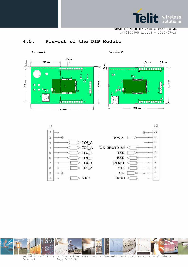
4.5. Pin-out of the DIP Module
Version 1 Version 2
xE50-433/868 RF Module User Guide 1VV0300905 Rev.13 – 2015-07-28
Reproduction forbidden without written authorizatio n from Telit Communications S.p.A. - All Rights Reserved. Page 35 of 50
4.6. Description of the signals
Signals Description
Reset External hardware reset of the radio module. Active on low state.
TXD, RXD Serial link signals, format NRZ/TTL: TXD is for outgoing data. RXD is for incoming data. The ‘1’ is represented by a high state.
CTS Incoming signal. Indicates whether the module can send serial data to user (Active, on low state) or not (inactive, on high state).
RTS Outgoing signal. Indicates whether the user can transmit serial data (active, on low state) or not (inactive, on high state).
IO I/O, configurable as input or as output. See reference document [7] for LE50-868. Available upon request for NE50-433, NE50-868 and ME50-868
STANDBY (LE50-433/868)
Input signal which indicates to the module to switch to pre-selected low-power mode. See reference document [7] for LE50-433/868
WAKEUP (NE50-433/868, ME50-868)
Input signal which indicates to the module to wake up from low-power mode. See reference document document [8] for NE50-433/868 and document [9] for ME50-868..
TX LED (LE50-433 and LE50-868 only)
Output signal set to VCC during radio transmission and set to GND the rest of the time
RX LED (LE50-433 and LE50-868 only)
Output signal set to VCC as soon as a radio frame is detected with correct synchronization word. The signal returns to GND as soon as the frame reception is finished
ACK TX (LE50-433 and LE50-868 only)
In Addressed Secured mode, this signal rises to VCC when an ACK hasn’t been received after frame transmission and repetition. This is the hardware version of “ERROR” serial message. It stays at VCC until next success addressed secured transmission
STATUS TX/RX (LE50-433 and LE50-868 only)
Output signal which indicates the status of the serial port. When serial port is transmitting, Status RX/TX signal goes VCC until the end of serial transmission. The signal stays to GND the rest of the time
ASSO (NE50-868 and NE50-433 only)
The ‘ASSO’ output signal is set to logical ‘1’ continuously when the module is connected to the network. The output signal value changes fast when the module is not connected to the network and the value changes slowly when a valid network has been found and the device is looking for the best parent into this network.
STANDBY STATUS (NE50-433/868 and ME50-868 only)
The ‘STAND BY STATUS’ output signal is set to logical ‘1’ while the module is operating and return to ‘0’ during stand by periods.
xE50-433/868 RF Module User Guide 1VV0300905 Rev.13 – 2015-07-28
Reproduction forbidden without written authorizatio n from Telit Communications S.p.A. - All Rights Reserved. Page 36 of 50
5. Process Information
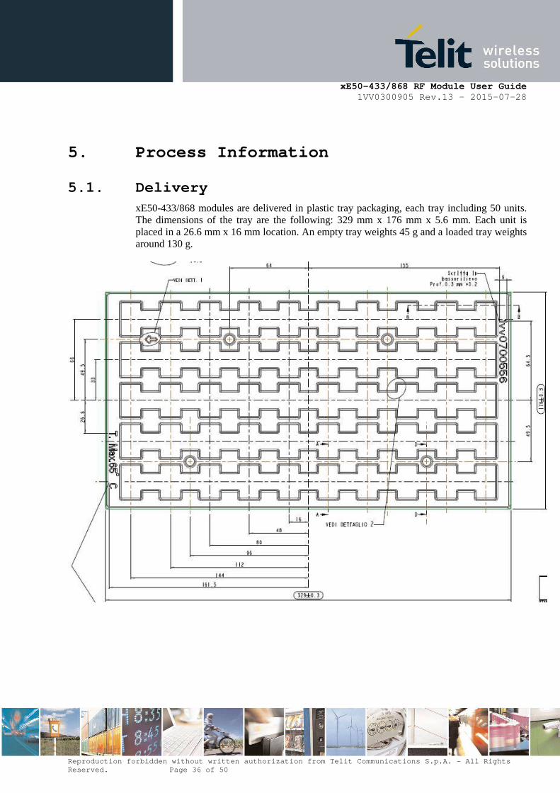
5.1. Delivery xE50-433/868 modules are delivered in plastic tray packaging, each tray including 50 units. The dimensions of the tray are the following: 329 mm x 176 mm x 5.6 mm. Each unit is placed in a 26.6 mm x 16 mm location. An empty tray weights 45 g and a loaded tray weights around 130 g.
xE50-433/868 RF Module User Guide 1VV0300905 Rev.13 – 2015-07-28
Reproduction forbidden without written authorizatio n from Telit Communications S.p.A. - All Rights Reserved. Page 37 of 50
5.2. Storage The optimal storage environment for ME70-169 modules should be dust free, dry and the temperature should be included between -40°C and +85°C.
5.3. Moisture sensibility The level of moisture sensibility of the Product is “3” according with standard IPC/JEDEC JSTD-020, take care of all the relative requirements for using this kind of components. Moreover, the customer has to take care of the following conditions: a) The shelf life of the Product inside of the dry bag must be 12 months from the bag seal
date, b) when stored in a non-condensing atmospheric environment of <= 30°C / 60% RH
according to IPC/JEDEC J-STD-033A paragraph 5 c) The maximum time between the opening of the sealed bag and the reflow process must be
168 hours if condition b) “IPC/JEDEC J-STD-033A paragraph 5.2” is respected d) Baking is required if conditions b) or c) are not respected e) Baking is required if the humidity indicator inside the bag indicates 10% RH or more.
5.4. Additional Precautions Also, it must be noted that due to some components, ME70-169 modules are ESD sensitive
device. Therefore, ESD handling precautions should be carefully observed.
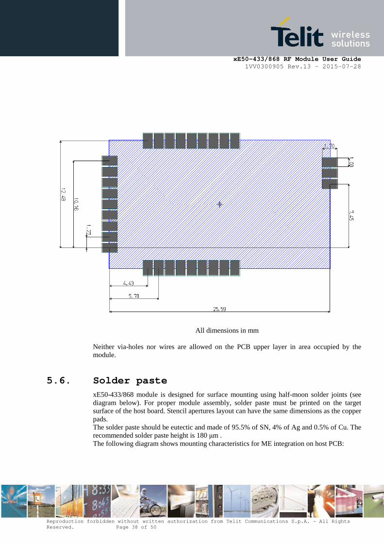
5.5. Soldering pad pattern The surface finished on the printed circuit board pads should be made of Nickel/Gold surface. The recommended soldering pad layout on the host board for the xE50-433/868 is shown in the diagram below:
xE50-433/868 RF Module User Guide 1VV0300905 Rev.13 – 2015-07-28
Reproduction forbidden without written authorizatio n from Telit Communications S.p.A. - All Rights Reserved. Page 38 of 50
All dimensions in mm
Neither via-holes nor wires are allowed on the PCB upper layer in area occupied by the module.
5.6. Solder paste xE50-433/868 module is designed for surface mounting using half-moon solder joints (see diagram below). For proper module assembly, solder paste must be printed on the target surface of the host board. Stencil apertures layout can have the same dimensions as the copper pads. The solder paste should be eutectic and made of 95.5% of SN, 4% of Ag and 0.5% of Cu. The recommended solder paste height is 180 µm . The following diagram shows mounting characteristics for ME integration on host PCB:
xE50-433/868 RF Module User Guide 1VV0300905 Rev.13 – 2015-07-28
Reproduction forbidden without written authorizatio n from Telit Communications S.p.A. - All Rights Reserved. Page 39 of 50
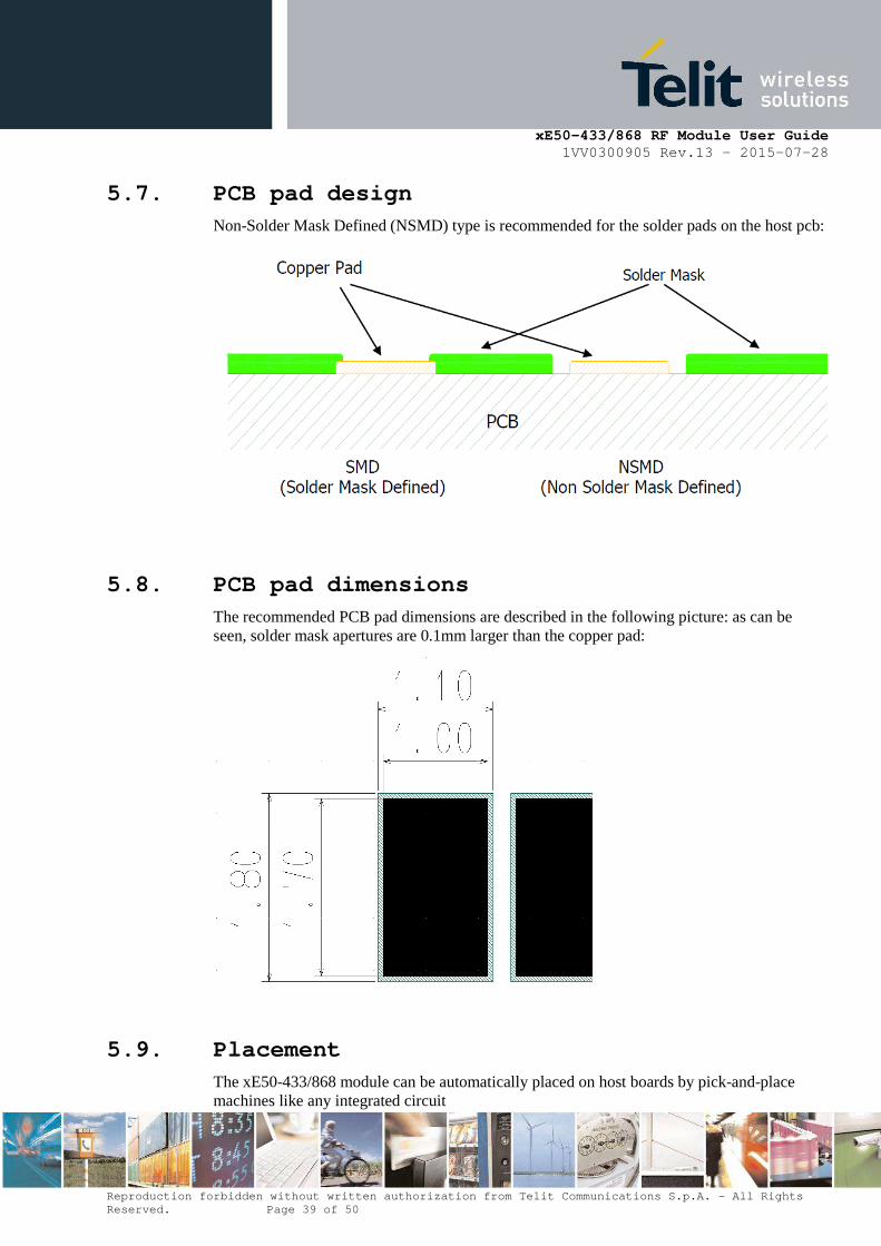
5.7. PCB pad design Non-Solder Mask Defined (NSMD) type is recommended for the solder pads on the host pcb:
5.8. PCB pad dimensions The recommended PCB pad dimensions are described in the following picture: as can be seen, solder mask apertures are 0.1mm larger than the copper pad:
5.9. Placement The xE50-433/868 module can be automatically placed on host boards by pick-and-place machines like any integrated circuit
xE50-433/868 RF Module User Guide 1VV0300905 Rev.13 – 2015-07-28
Reproduction forbidden without written authorizatio n from Telit Communications S.p.A. - All Rights Reserved. Page 40 of 50
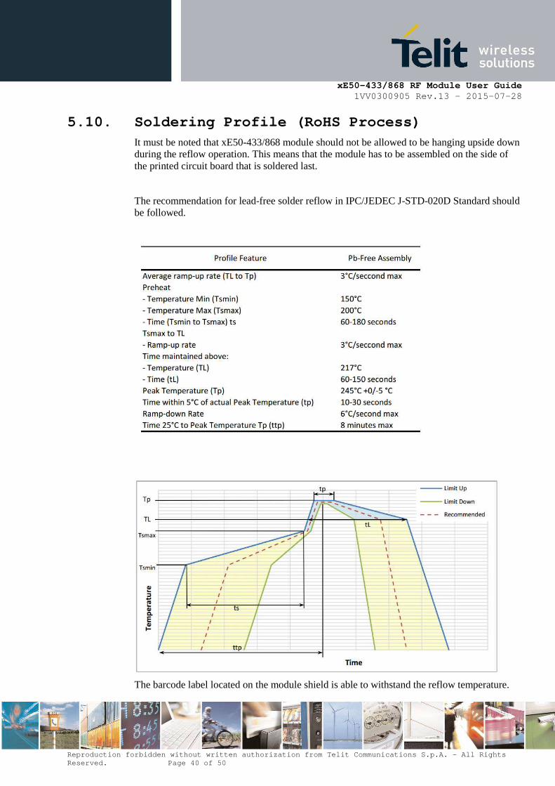
5.10. Soldering Profile (RoHS Process) It must be noted that xE50-433/868 module should not be allowed to be hanging upside down during the reflow operation. This means that the module has to be assembled on the side of the printed circuit board that is soldered last.
The recommendation for lead-free solder reflow in IPC/JEDEC J-STD-020D Standard should be followed.
The barcode label located on the module shield is able to withstand the reflow temperature.
xE50-433/868 RF Module User Guide 1VV0300905 Rev.13 – 2015-07-28
Reproduction forbidden without written authorizatio n from Telit Communications S.p.A. - All Rights Reserved. Page 41 of 50
CAUTION - It must also be noted that if the host board is submitted to a wave soldering after the reflow operation, a solder mask must be used in order to protect the xE50-433/868 radio module’s metal shield from being in contact with the solder wave.
xE50-433/868 RF Module User Guide 1VV0300905 Rev.13 – 2015-07-28
Reproduction forbidden without written authorizatio n from Telit Communications S.p.A. - All Rights Reserved. Page 42 of 50
6. Board Mounting Recommendation
6.1. Electrical environment The best performances of the xE50-433/868 module are obtained in a “clean noise” environment. Some basic recommendations must be followed:
• Noisy electronic components (serial RS232, DC-DC Converter, Display, Ram, bus ,...) must be placed as far as possible from the LE50-868 module.
• Switching components circuits (especially RS-232/TTL interface circuit power supply) must be decoupled with a 100 µF tantalum capacitor. And the decoupling capacitor must be as close as possible to the noisy chip.
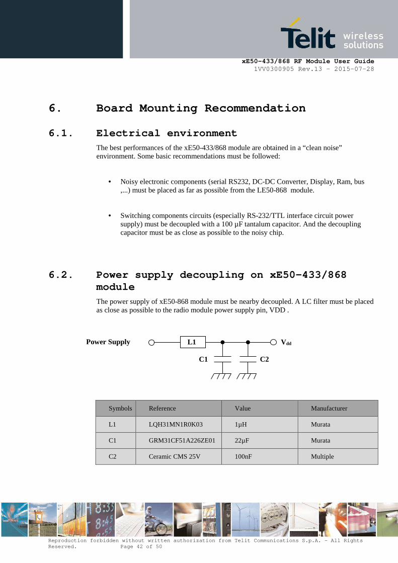
6.2. Power supply decoupling on xE50-433/868 module The power supply of xE50-868 module must be nearby decoupled. A LC filter must be placed as close as possible to the radio module power supply pin, VDD .
Symbols Reference Value Manufacturer
L1 LQH31MN1R0K03 1µH Murata
C1 GRM31CF51A226ZE01 22µF Murata
C2 Ceramic CMS 25V 100nF Multiple
Vdd
C1 C2
Power Supply
L1
xE50-433/868 RF Module User Guide 1VV0300905 Rev.13 – 2015-07-28
Reproduction forbidden without written authorizatio n from Telit Communications S.p.A. - All Rights Reserved. Page 43 of 50
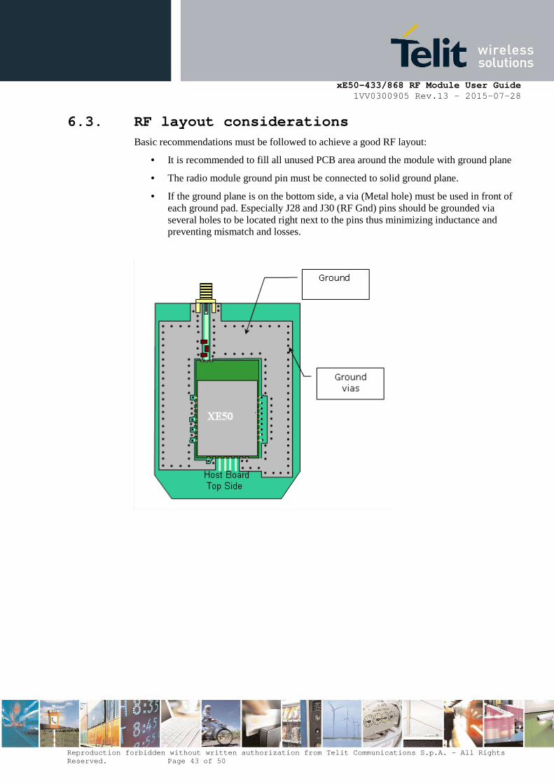
6.3. RF layout considerations Basic recommendations must be followed to achieve a good RF layout:
• It is recommended to fill all unused PCB area around the module with ground plane
• The radio module ground pin must be connected to solid ground plane.
• If the ground plane is on the bottom side, a via (Metal hole) must be used in front of each ground pad. Especially J28 and J30 (RF Gnd) pins should be grounded via several holes to be located right next to the pins thus minimizing inductance and preventing mismatch and losses.

xE50-433/868 RF Module User Guide 1VV0300905 Rev.13 – 2015-07-28
Reproduction forbidden without written authorizatio n from Telit Communications S.p.A. - All Rights Reserved. Page 44 of 50
6.4. Antenna connections on printed circuit boards Special care must be taken when connecting an antenna or a connector to the module. The RF output impedance is 50 ohms, so the strip between the pad and the antenna or connector must be 50 ohms following the tables below. Ground lines should be connected to the ground plane with as many vias as possible, but not too close to the signal line.
PCB material PCB thickness H (mm) Coplanar line W (mm) Coplanar line G (mm)
FR4 0.8 1 0.3
1.6 1 0.2
Table 1 : Values for double face PCB with ground plane around and under coplanar wave guide (recommended)
PCB material PCB thickness H (mm) Coplanar line W (mm) Coplanar line G (mm)
FR4 0.8 1 0.22
1.6 1 0.23
Table 2 : Values for simple face PCB with ground plane around coplanar wave guide (not recommended)
xE50-433/868 RF Module User Guide 1VV0300905 Rev.13 – 2015-07-28
Reproduction forbidden without written authorizatio n from Telit Communications S.p.A. - All Rights Reserved. Page 45 of 50
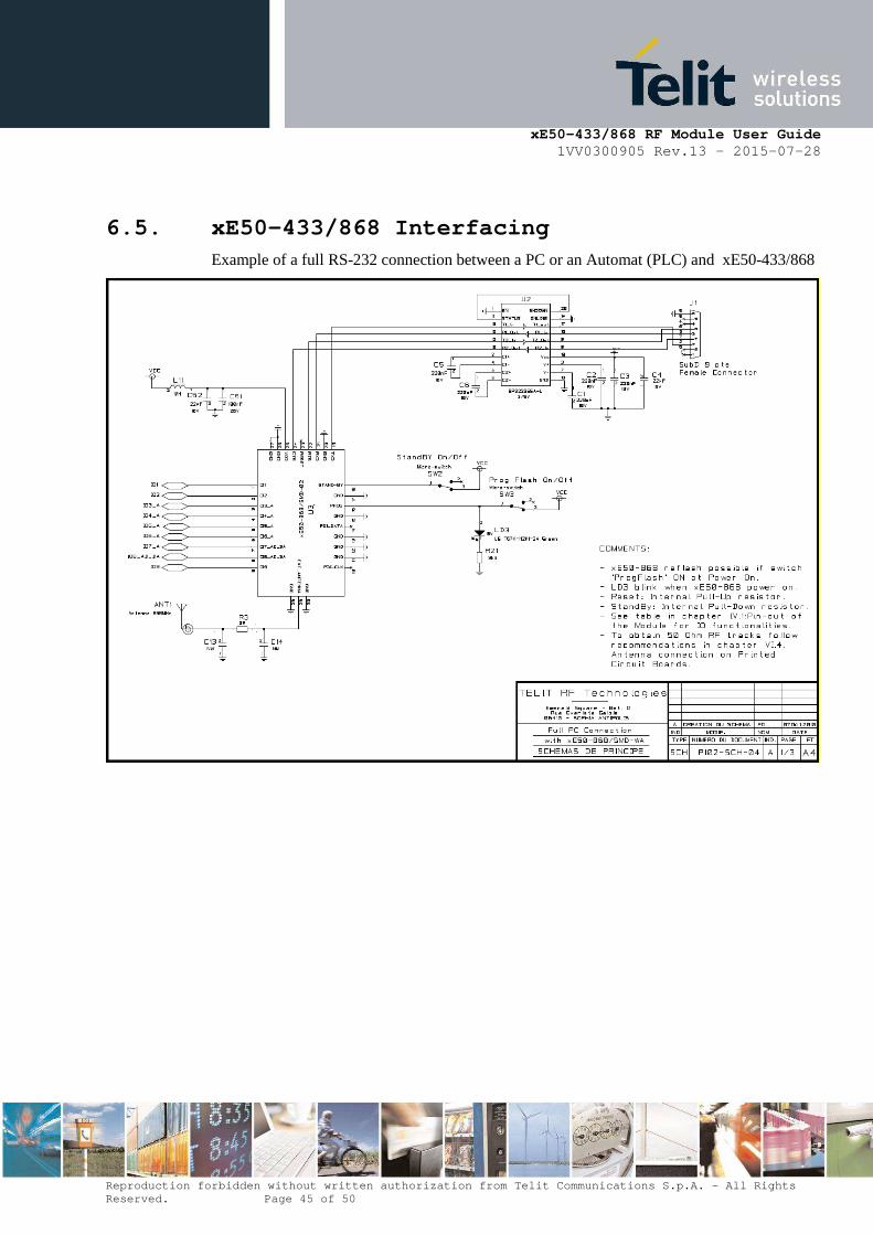
6.5. xE50-433/868 Interfacing Example of a full RS-232 connection between a PC or an Automat (PLC) and xE50-433/868
xE50-433/868 RF Module User Guide 1VV0300905 Rev.13 – 2015-07-28
Reproduction forbidden without written authorizatio n from Telit Communications S.p.A. - All Rights Reserved. Page 46 of 50
7. Annexes
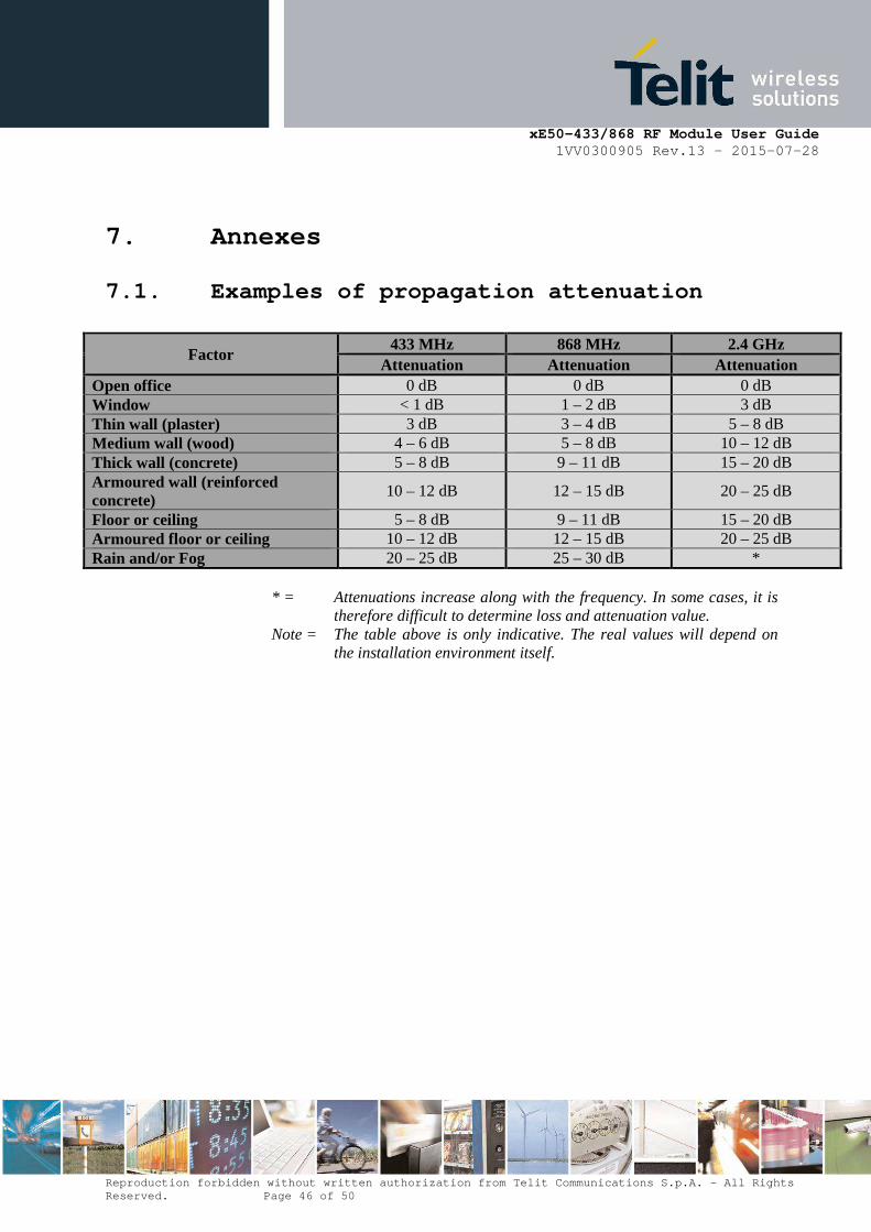
7.1. Examples of propagation attenuation
Factor 433 MHz 868 MHz 2.4 GHz
Attenuation Attenuation Attenuation Open office 0 dB 0 dB 0 dB Window < 1 dB 1 – 2 dB 3 dB Thin wall (plaster) 3 dB 3 – 4 dB 5 – 8 dB Medium wall (wood) 4 – 6 dB 5 – 8 dB 10 – 12 dB Thick wall (concrete) 5 – 8 dB 9 – 11 dB 15 – 20 dB Armoured wall (reinforced concrete)
10 – 12 dB 12 – 15 dB 20 – 25 dB
Floor or ceiling 5 – 8 dB 9 – 11 dB 15 – 20 dB Armoured floor or ceiling 10 – 12 dB 12 – 15 dB 20 – 25 dB Rain and/or Fog 20 – 25 dB 25 – 30 dB *
* = Attenuations increase along with the frequency. In some cases, it is
therefore difficult to determine loss and attenuation value. Note = The table above is only indicative. The real values will depend on
the installation environment itself.

xE50-433/868 RF Module User Guide 1VV0300905 Rev.13 – 2015-07-28
Reproduction forbidden without written authorizatio n from Telit Communications S.p.A. - All Rights Reserved. Page 47 of 50
7.2. Declaration of conformity

xE50-433/868 RF Module User Guide 1VV0300905 Rev.13 – 2015-07-28
Reproduction forbidden without written authorizatio n from Telit Communications S.p.A. - All Rights Reserved. Page 48 of 50
8. Safety Recommendations
READ CAREFULLY Be sure the use of this product is allowed in the country and in the environment required. The use of this product may be dangerous and has to be avoided in the following areas:
• Where it can interfere with other electronic devices in environments such as hospitals, airports, aircrafts, etc.
• Where there is risk of explosion such as gasoline stations, oil refineries, etc. It is responsibility of the user to enforce the country regulation and the specific environment regulation.
Do not disassemble the product; any mark of tampering will compromise the warranty validity. We recommend following the instructions of the hardware user guides for a correct wiring of the product. The product has to be supplied with a stabilized voltage source, Safety Extra Low Voltage, with no energy hazard. The wiring has to be conforming to the security and fire prevention regulations. The product has to be handled with care, avoiding any contact with the pins because electrostatic discharges may damage the product itself. The system integrator is responsible of the functioning of the final product; therefore, care has to be taken to the external components of the module, as well as of any project or installation issue, because the risk of disturbing external devices or having impact on the security. Should there be any doubt, please refer to the technical documentation and the regulations in force. When installed in final product, a fire protection enclosure must be provided. Every module has to be equipped with a proper antenna with specific characteristics. The antenna has to be installed with care in order to avoid any interference with other electronic devices and has to guarantee a minimum distance from the body (20 cm). The European Community provides some Directives for the electronic equipments introduced on the market. All the relevant information’s are available on the European Community website: http://ec.europa.eu/enterprise/sectors/rtte/documents/ The text of the Directive 99/05 regarding telecommunication equipments is available, while the applicable Directives (Low Voltage and EMC) are available at: http://ec.europa.eu/enterprise/sectors/electrical/

xE50-433/868 RF Module User Guide 1VV0300905 Rev.13 – 2015-07-28
Reproduction forbidden without written authorizatio n from Telit Communications S.p.A. - All Rights Reserved. Page 49 of 50
9. Glossary
ACP Adjacent Channel Power AFA Adaptive Frequency Agility bps Bits per second BW Bandwidth dB Decibel dBm Power level in decibel milliwatt (10 log (P/1mW)) E2PROM Electrically Erasable Programmable Read Only Memory e.r.p Effective radiated power ETSI European Telecommunication Standard Institute GFSK Gaussian Frequency Shift Keying I Input ISM Industrial, Scientific and Medical kB KiloByte kbps Kilobits per second kcps Kilochips per second kHz Kilo Hertz LBT Listen Before Talk LGA Land Grid Array MHz Mega Hertz mW milliwatt O Output PER Packet Error Rate ppm Parts per million RAM Random Access Memory RF Radio Frequency RoHS Restriction of Hazardous Substances RxD Receive Data SMD Surface Mounted Device SRD Short Range Device TxD Transmit Data UART Universal Asynchronous Receiver Transmitter µC microcontroller

xE50-433/868 RF Module User Guide 1VV0300905 Rev.13 – 2015-07-28
Reproduction forbidden without written authorizatio n from Telit Communications S.p.A. - All Rights Reserved. Page 50 of 50
10. Document History
Revision Date Changes 0 2011-02-22 First Release 1 2011-05-18 • Updated pin-out table
• New DIP module • Adding RF Layout drawing
2 2011-06-23 • Updated Related Documents • Added a table in 3.5
3 2011-07-05 • Updated 2.1 • Updated 3.5
4 2011-07-27 • Users Guides “NE50-868 RF Module User Guide 1vv0300897” and “ME50-868 RF Module User Guide 1vv0300892” are integrated into the present User Guide
• Added 7.2 5 2011-08-10 • Updated 1.4
• Updated 3.8 • Updated 3.10 • Updated 4.3 • Updated 4.4
6 2011-09-20 • Name of the present User Guide is updated • LE50-433 module is integrated in the present User
Guide • Updated 3.9 • Updated 3.11
7 2011-12-16 • NE50-433 module is integrated in the present User Guide
8 2012-03-14 • Updated J18 Pin description in 4.2 • Updated J2 and J18 Pin name and description in
4.3 • Updated J1, J2, J18 Pin name and description in
4.4 • Updated 4.5 • Updated 4.6
9 2012-06-14 • Updated 3.5 to 3.8 with modified output power level steps
• Updated 7.2 • Updated 8
10 2012-09-28 • Updated 7.2 11 2012-06-20 • Updated 3.5 to 3.9 & 1.6 & 2.1& 2.6 12 2015-06-19 • Updated Process Information 13 2015-07-28 • Updated mounting footprint information