Embed Size (px)
Citation preview

XAPP1164 (v1.0) May 9, 2013 www.xilinx.com 1
© Copyright 2013 Xilinx, Inc. Xilinx, the Xilinx logo, Artix, ISE, Kintex, Spartan, Virtex, Vivado, Zynq, and other designated brands included herein are trademarks of Xilinx in the United States and other countries. All other trademarks are the property of their respective owners.
Summary A Multi-Port Memory Controller (MPMC) is used in applications where multiple devices share a common memory controller. An MPMC is a common requirement in many video, embedded, and communications applications where data from multiple sources moves through a common memory device, typically DDR3 SDRAM.
This application note demonstrates how to create a basic DDR3 MPMC design using a 7 series FPGA and the IP integrator tool within the Vivado® Design Suite[Ref 1]. The MPMC is created by combining the Memory Interface Generator (MIG) core and the AXI Interconnect IP, both of which are provided in the Vivado tools.
AXI is a standardized IP interface protocol based on the Advanced Microcontroller Bus Architecture (AMBA® 4) specification [Ref 2]. This reference design uses the AXI4, AXI4-Lite, and AXI4-Stream interfaces as described in the AXI4 specification. These interfaces provide a common IP interface protocol framework for building the system.
Overview The example design in this application note is a full working hardware system on the KC705 evaluation board in the Xilinx® Kintex™-7 FPGA KC705 Evaluation Kit [Ref 3].
The design implements a basic video system where data from a video Test Pattern Generator (TPG) loops in and out of memory multiple times before being sent to the High-Definition Multimedia Interface (HDMI) technology connector on the board, as follows:
• The DDR3 memory acts as a multi-ported memory being shared by multiple video frame buffers.
• Two AXI Video Direct Memory Access (AXI VDMA) cores control the video frame buffers.
• Each AXI VDMA takes AXI4-Stream data carrying video information and moves the data to or from memory over AXI4 interfaces.
• The AXI Interconnect acts as an arbitrated switch to multiplex AXI4 transactions to the shared memory controller, thus creating an AXI MPMC system.
• A clock generator block supplies clocks throughout the system.
• AXI4-Lite master cores generate the necessary configuration commands to set up the AXI VDMA after reset.
Application Note: 7 Series FPGAs
XAPP1164 (v1.0) May 9, 2013
7 Series FPGAs AXI Multi-Port Memory Controller Using the Vivado IP Integrator ToolAuthor: Khang Dao, Sikta Pany, and Ricky Su

Overview
XAPP1164 (v1.0) May 9, 2013 www.xilinx.com 2
The design uses the Vivado® Design Suite IP integrator tool. The IP integrator is a block-based design and assembly tool that provides a higher level of automation than building the equivalent system using the Vivado tool logic design flow. Vivado IP integrator is used to assemble many of the key blocks of the design into a subsystem. This subsystem is instantiated inside a higher level HDL design and is connected to additional HDL logic to illustrate how to build and integrate subsystems into a complete design.
Figure 1 provides a block diagram of the system and illustrates the basic data flow in the system.
X-Ref Target - Figure 1
Figure 1: Overview of AXI MPMC System

Quick Start
XAPP1164 (v1.0) May 9, 2013 www.xilinx.com 3
Quick Start This section provides the steps to build the design starting from the complete project file set and also shows how to run the demonstration design on the KC705 board.
Note: Instructions to build the design from a new Vivado tools project are covered in Creating the AXI MPMC Design from a New Vivado Project, page 12.
Steps to Open and Rebuild the Design
To open and rebuild the design:
1. Install the Vivado Design Suite 2013.1 (requires a license to use the Vivado IP integrator tool)
2. Install the ISE® Design Suite or ISE Lab Tools 14.5. This installs the iMPACT tool that can be used for downloading the bitstreams.
3. Unzip the reference design files accompanying this application note into a local folder (referred to as <design_dir>).
To run the pre-generated bitstream in hardware without rebuilding the design, go to step 8, page 5
Otherwise, continue with these instructions to rebuild the design:
4. After setting up the Xilinx tools, open the Vivado Integrated Design Environment (IDE):
• In Windows, select Start > Xilinx Design Tools > Vivado 2013.1> Vivado 2013.1.
• In Linux, enter the vivado command.
5. In the Vivado Integrated Development Environment (IDE), select Getting Started > Open Project (Figure 2).

Quick Start
XAPP1164 (v1.0) May 9, 2013 www.xilinx.com 4
6. Select Browse Projects, and choose <design_dir>/vivado/project_1/project_1.xpr (Figure 3).
7. Select Flow > Generate Bitstream, (Figure 4) or, from the Flow Navigator, select Program and Debug > Generate Bitstream (Figure 5).
Note: If a dialog displays asking to run synthesis and implementation, click Yes. The process to run synthesis and implementation on this design can take one hour or longer to complete.
X-Ref Target - Figure 2
Figure 2: Getting Started Dialog Box
X-Ref Target - Figure 3
Figure 3: Browse Project Dialog Box

Quick Start
XAPP1164 (v1.0) May 9, 2013 www.xilinx.com 5
8. When the Bitstream Generation Completed opens, click Cancel to return to the Vivado GUI (Figure 6).
X-Ref Target - Figure 4
Figure 4: Generate Bitstream Option
X-Ref Target - Figure 5
Figure 5: Starting Bitstream Generation Using Icon
X-Ref Target - Figure 6
Figure 6: Bitstream Generation Completed

Quick Start
XAPP1164 (v1.0) May 9, 2013 www.xilinx.com 6
KC705 Board Setup1. The reference design runs on the KC705 board (Rev D), as shown in
Figure 7.
2. Connect the USB cable (provided with the board) from the host PC to the USB JTAG port (1 in Figure 7) of the KC705 board. Ensure that the appropriate device drivers are installed.
3. Connect the HDMI connector of the KC705 board to a video monitor capable of displaying a 1280 x 720p, 60 Hz video signal (2 in Figure 7).
4. Connect the power supply cable to the KC705 board (3 in Figure 7).
5. Turn on the power to the KC705 board (4 in Figure 7).
X-Ref Target - Figure 7
Figure 7: KC705 Board Photo
1
2
3
4

Quick Start
XAPP1164 (v1.0) May 9, 2013 www.xilinx.com 7
Download and Run Bitstream
If the design was not rebuilt, and if you are going to use the pre-generated bitstream included in the design files to program the KC705 board, perform step 1. If the design has already been rebuilt in the Vivado tools and the project is open, go to step 2.
1. Open iMPACT directly by selecting Start > Xilinx Design Tools > ISE Design Suite 14.5 > ISE Design Tools > (32 or64)-bit Tools > iMPACT or enter impact at the command line in Linux, and go to step .
2. Run iMPACT by selecting Flow > Launch iMPACT from the Vivado tools menu bar (Figure 8) or click the icon next to Program and Debug > Launch iMPACT (Figure 9).
X-Ref Target - Figure 8
Figure 8: Running iMPACT Using Menu Options

Quick Start
XAPP1164 (v1.0) May 9, 2013 www.xilinx.com 8
The iMPACT wizard launches automatically.
3. If it does not launch, select Edit > Launch Wizard (Figure 10).
4. In the Welcome to iMPACT dialog box, select Configure devices using Boundary-Scan (JTAG), and click OK (Figure 11).
X-Ref Target - Figure 9
Figure 9: Running iMPACT Using Icons
X-Ref Target - Figure 10
Figure 10: Launching iMPACT Wizard
X-Ref Target - Figure 11
Figure 11: Welcome to iMPACT Dialog Box

Quick Start
XAPP1164 (v1.0) May 9, 2013 www.xilinx.com 9
5. In the Auto Assign Configuration Files Query Dialog box, click Yes (Figure 12).
6. Browse to <design_dir>/vivado/project_1.runs/impl_1, select top.bit, and click Open (Figure 13).
Note: If the design was not rebuilt using the Vivado tools, download the pre-generated bitstream file by opening <design_dir>/ready_to_download/top.bit.
7. For SPI or BPI PROM options, click No (Figure 14).
X-Ref Target - Figure 12
Figure 12: Auto Assign Configuration Files Query Dialog Box
X-Ref Target - Figure 13
Figure 13: Assign New Configuration File Dialog Box
X-Ref Target - Figure 14
Figure 14: Attach SPI or BPI PROM Dialog Box

Quick Start
XAPP1164 (v1.0) May 9, 2013 www.xilinx.com 10
8. In the Device Programming Properties dialog box, click OK (Figure 15).
Program the FPGA9. Right-click the xc7k325t device and select Program (Figure 16).
X-Ref Target - Figure 15
Figure 15: Device Programming Properties Dialog Box
X-Ref Target - Figure 16
Figure 16: Programming the FPGA

Quick Start
XAPP1164 (v1.0) May 9, 2013 www.xilinx.com 11
After the design is downloaded, the video monitor shows a number of white circular ripple patterns that slowly move outward (Figure 17). This demonstrates a live AXI MPMC system in hardware moving multiple frames of video data through DDR3 memory controlled by two AXI VDMA IP blocks.
X-Ref Target - Figure 17
Figure 17: Video Image Displayed on Monitor When KC705 Board is Programmed
Creating the AXI MPMC Design from a New Vivado Project
XAPP1164 (v1.0) May 9, 2013 www.xilinx.com 12
Creating the AXI MPMC Design from a New Vivado Project
This section provides the steps to build the design starting from a new Vivado tools project. It describes how to use the Vivado Design Suite to add or configure IP blocks to the project, connect them together into a system, and implement the design to a bitstream.
Note: Figures might show additional configuration or GUI options than those listed in the instructions. In these cases leave the option at its default value unless instructed to change the setting.
Start a New Vivado Project and Set the Project Options1. Install the Vivado Design Suite 2013.1 (requires a license to use the Vivado
IP integrator tool).
Note: An Early Access license for Vivado IP Integrator is required with 2013.1. To obtain a license, contact your Xilinx Field Application Engineer.
2. Unzip the reference design files into a local folder (referred to as <design_dir>).
3. After setting up the Xilinx tools, open the Vivado Integrated Design Environment (IDE):
• In Windows, select Start > Xilinx Design Tools > Vivado 2013.1> Vivado 2013.1.
• In Linux, enter the vivado command in Linux.
4. Create a new project by selecting Getting Started > Create New Project, refer to Figure 2, page 4.
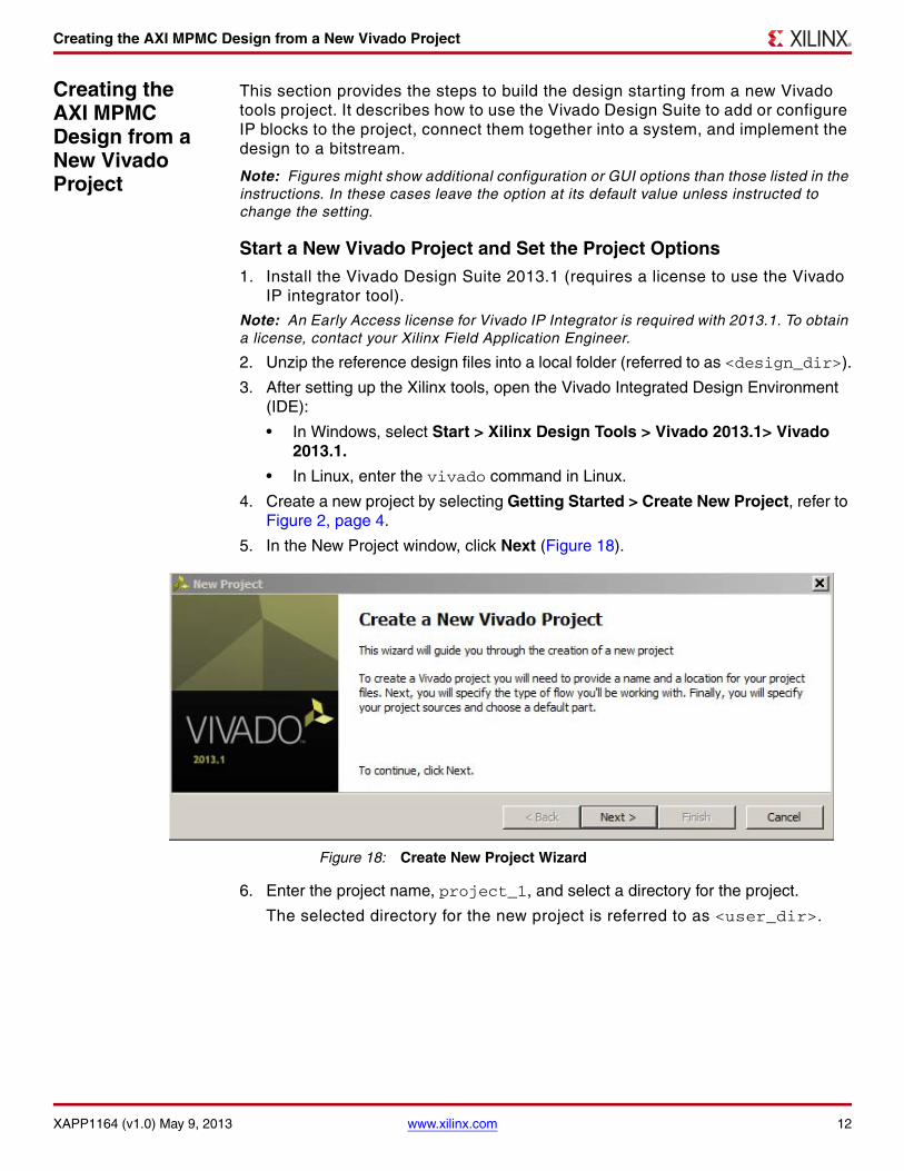
5. In the New Project window, click Next (Figure 18).
6. Enter the project name, project_1, and select a directory for the project.
The selected directory for the new project is referred to as <user_dir>.
X-Ref Target - Figure 18
Figure 18: Create New Project Wizard

Creating the AXI MPMC Design from a New Vivado Project
XAPP1164 (v1.0) May 9, 2013 www.xilinx.com 13
7. In the Project Type dialog box, select RTL Project (Figure 19).
8. In the following dialog boxes, click Next:
• Add Sources
• Add Existing IP
• Add Constraints
The New Project Default Part dialog box opens.
X-Ref Target - Figure 19
Figure 19: New Project Window (Project Type)
Creating the AXI MPMC Design from a New Vivado Project
XAPP1164 (v1.0) May 9, 2013 www.xilinx.com 14
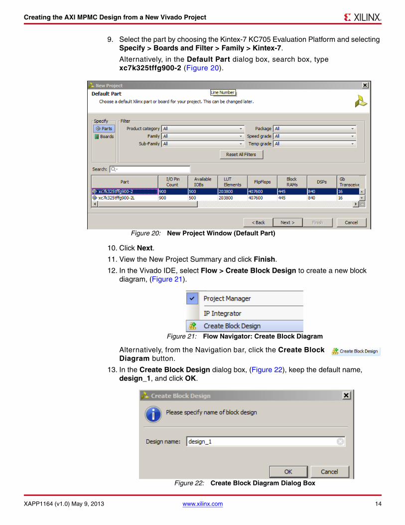
9. Select the part by choosing the Kintex-7 KC705 Evaluation Platform and selecting Specify > Boards and Filter > Family > Kintex-7.
Alternatively, in the Default Part dialog box, search box, type xc7k325tffg900-2 (Figure 20).
10. Click Next.
11. View the New Project Summary and click Finish.
12. In the Vivado IDE, select Flow > Create Block Design to create a new block diagram, (Figure 21).
Alternatively, from the Navigation bar, click the Create Block Diagram button.
13. In the Create Block Design dialog box, (Figure 22), keep the default name, design_1, and click OK.
X-Ref Target - Figure 20
Figure 20: New Project Window (Default Part)
X-Ref Target - Figure 21
Figure 21: Flow Navigator: Create Block Diagram
X-Ref Target - Figure 22
Figure 22: Create Block Diagram Dialog Box

Creating the AXI MPMC Design from a New Vivado Project
XAPP1164 (v1.0) May 9, 2013 www.xilinx.com 15
Adding the Memory Controller (MIG IP Core) to the Design
To add the Memory controller:
1. Right-click the diagram and, from the popup menu, (Figure 23),select Add IP or click the Add IP button on the Diagram toolbar to open the IP Catalog window.
2. In the Search bar, type MIG to find the MIG 7 series IP.
The IP integrator adds the symbol for the MIG 7 series IP to IP integrator diagram.
3. Double-click the IP symbol, (Figure 24), to configure the MIG IP.
X-Ref Target - Figure 23
Figure 23: Add IP Popup Menu
X-Ref Target - Figure 24
Figure 24: Initial MIG Symbol in Block Diagram

Creating the AXI MPMC Design from a New Vivado Project
XAPP1164 (v1.0) May 9, 2013 www.xilinx.com 16
4. In the MIG GUI, review the Vivado project options, and click Next (Figure 25).
5. Choose Create Design, and click Next (Figure 26). K
X-Ref Target - Figure 25
Figure 25: Kintex 7- FPGA Memory Interface Generator (MIG) Front Page
X-Ref Target - Figure 26
Figure 26: MIG Output Options

Creating the AXI MPMC Design from a New Vivado Project
XAPP1164 (v1.0) May 9, 2013 www.xilinx.com 17
6. For Pin Compatible FPGAs settings, (Figure 27), click Next.
This page is normally used for a new board pinout definition that is desired to be compatible across multiple devices in the same package.
7. Click Memory Selection, select DDR3 SDRAM, then click Next (Figure 28).
This creates a memory controller for the DDR3 memory on the KC705 board that has an AXI Interface to later connect to the AXI Interconnect IP.
X-Ref Target - Figure 27
Figure 27: MIG Pin-Compatible Virtex-7 FPGAs
X-Ref Target - Figure 28
Figure 28: MIG Memory Type and Controller Selection

Creating the AXI MPMC Design from a New Vivado Project
XAPP1164 (v1.0) May 9, 2013 www.xilinx.com 18
8. In Controller Options, (Figure 29), set the following:
a. Clock Period: 2500 ps: Sets the design for a 400 MHz memory clock. This clock frequency is supported for the device and speed grade of a KC705 FPGA.
b. Set the memory information to match the KC705 (SODIMM Memory Type, MT8JTF12864HZ-1G6 Memory Part).
c. Scroll down the page as needed to ensure that the Data Mask option is checked (default) and Ordering is set to Normal (default).
d. Click Next.X-Ref Target - Figure 29
Figure 29: MIG Controller Options Page
Creating the AXI MPMC Design from a New Vivado Project
XAPP1164 (v1.0) May 9, 2013 www.xilinx.com 19
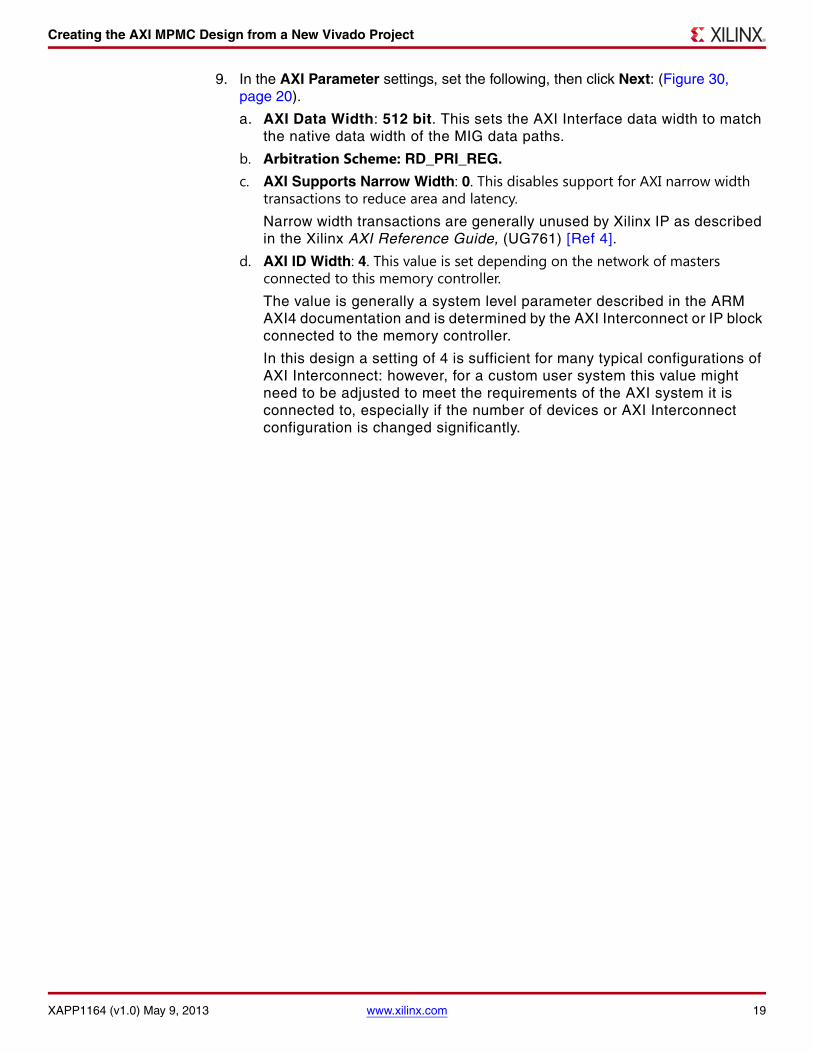
9. In the AXI Parameter settings, set the following, then click Next: (Figure 30, page 20).
a. AXI Data Width: 512 bit. This sets the AXI Interface data width to match the native data width of the MIG data paths.
b. Arbitration Scheme: RD_PRI_REG. c. AXI Supports Narrow Width: 0. This disables support for AXI narrow width
transactions to reduce area and latency. Narrow width transactions are generally unused by Xilinx IP as described in the Xilinx AXI Reference Guide, (UG761) [Ref 4].
d. AXI ID Width: 4. This value is set depending on the network of masters connected to this memory controller. The value is generally a system level parameter described in the ARM AXI4 documentation and is determined by the AXI Interconnect or IP block connected to the memory controller.
In this design a setting of 4 is sufficient for many typical configurations of AXI Interconnect: however, for a custom user system this value might need to be adjusted to meet the requirements of the AXI system it is connected to, especially if the number of devices or AXI Interconnect configuration is changed significantly.

Creating the AXI MPMC Design from a New Vivado Project
XAPP1164 (v1.0) May 9, 2013 www.xilinx.com 20
X-Ref Target - Figure 30
Figure 30: MIG AXI Parameter Options

Creating the AXI MPMC Design from a New Vivado Project
XAPP1164 (v1.0) May 9, 2013 www.xilinx.com 21
10. In Memory Options, select the following, then click Next (Figure 31).
a. Clock Period: 5000ps (200 MHz). This is the clock frequency input available in KC705 board.
b. Read Burst Type: Sequential (default). This is a recommended general setting given which indicates that the masters in the system are video devices generally using sequential bursts.
c. Output Driver Impedance Control: RZQ/7. This matches the design requirements of the KC705 board.
d. Controller Chip Select Pin: Enable (default). This selection enables an actively driven CS pin to the DDR3 memory.
e. RTT/ODT: RZQ/4. This matches the design requirements of the KC705 board.f. Use either Memory Address Mapping Selection setting.
Because the video devices in the system have long sequential access patterns, similar results are likely to be observed.
X-Ref Target - Figure 31
Figure 31: MIG Memory Mode Options

Creating the AXI MPMC Design from a New Vivado Project
XAPP1164 (v1.0) May 9, 2013 www.xilinx.com 22
11. In FPGA Options, select the following, then click Next, (Figure 32).
a. Use the default options for Differential System Clock to match the clock source on the KC705 board.
b. Reference Clock: Use System Clock so the system clock can be shared as the reference clock source.
c. System Reset Polarity: ACTIVE_HIGH. This matches the KC705 board.d. The remaining options can be left default. Leave the internal Vref unchecked.
Note: The setting of XADC instantiation is enabled by default. This matches the normal configuration of the KC705 board where MIG is the only IP in the design using the XADC block.
12. In Extended FPGA Options:
• Check the DCI Cascade checkbox.
• Ensure Internal Termination Impedance is set to 50 Ohms.
This matches the requirement for KC705 board.
X-Ref Target - Figure 32
Figure 32: MIG FPGA Options

Creating the AXI MPMC Design from a New Vivado Project
XAPP1164 (v1.0) May 9, 2013 www.xilinx.com 23
13. Click Next (Figure 33).
14. In Pin/Bank Selection Mode, choose Fixed Pin Out, then click Next (Figure 34).
This lets you enter predefined pin out information for an existing board like the KC705.
Note: The other option is for a new board design where the user desires to have the tool choose a pin out.
X-Ref Target - Figure 33
Figure 33: MIG Extended FPGA Options
X-Ref Target - Figure 34
Figure 34: MIG I/O Planning Options

Creating the AXI MPMC Design from a New Vivado Project
XAPP1164 (v1.0) May 9, 2013 www.xilinx.com 24
15. For Pin Selection a user would normally use the pulldown menus in the GUI to enter the pin out information for I/O signals required by the memory interface (Figure 35).
To save time, the MIG GUI has an option to read a UCF or XDC file to import the pinout information. The format of this file is described in the MIG documentation.
For this design:
a. Click Read XDC/UCF and enter the name of a file pre-generated for the KC705 to save time from entering each pin location manually.
b. Browse and select the file design_1_mig_7series_1_0.ucf or design_1_mig_7series_1_0.xdc in <design_dir>/src/ip/ mig_7series/user_design/constraints/.
c. Click Open to load the KC705 pinout information file. This returns you to the Pin Selection menu.
d. Click Validate to have the MIG tool check the pinout, then click Next. MIG only uses the UCF/XDC file format to save and read back memory interface pinout information.
This file is not used for I/O constraints in the implementation tools.
The Vivado tool uses XDC files generated by the MIG tool to specify I/O constraints for the implementation tools.
X-Ref Target - Figure 35
Figure 35: MIG Pin Selection Using an Existing Pinout

Creating the AXI MPMC Design from a New Vivado Project
XAPP1164 (v1.0) May 9, 2013 www.xilinx.com 25
16. For the System Signals Selection, set the sys_clk_p/n to AD12/AD11 (default), then click Next (Figure 36).
X-Ref Target - Figure 36
Figure 36: MIG System Signals Selection

Creating the AXI MPMC Design from a New Vivado Project
XAPP1164 (v1.0) May 9, 2013 www.xilinx.com 26
17. Review the summary, and click Next.
The Summary page shows the overall IP configuration settings (Figure 37).X-Ref Target - Figure 37
Figure 37: MIG Summary

Creating the AXI MPMC Design from a New Vivado Project
XAPP1164 (v1.0) May 9, 2013 www.xilinx.com 27
18. Review the License Agreement, click Accept, and then Next to have the Vivado tools deliver a memory simulation model for use in creating a simulation testbench (Figure 38). If the License agreement is declined, a separate model must be obtained to perform simulations with this IP core.
Note: This application note does not demonstrate the simulation flow.X-Ref Target - Figure 38
Figure 38: MIG Micron Model License Agreement

Creating the AXI MPMC Design from a New Vivado Project
XAPP1164 (v1.0) May 9, 2013 www.xilinx.com 28
19. This window mentions that important PCB information is contained in the User Guide that is accessible by clicking the button in the lower-left corner (Figure 39).
X-Ref Target - Figure 39
Figure 39: MIG PCB Information

Creating the AXI MPMC Design from a New Vivado Project
XAPP1164 (v1.0) May 9, 2013 www.xilinx.com 29
20. Review the Design Notes and click Generate (Figure 40).
The MIG IP files are generated as the IP customization GUI is running to create the underlying HDL and constraint files.
After several seconds for the generation process to complete, control is returned to the Vivado tools.
This creates a memory controller for the DDR3 memory on the KC705 board that has an AXI Interface to later connect to the AXI Interconnect IP.
X-Ref Target - Figure 40
Figure 40: MIG Design Notes

Creating the AXI MPMC Design from a New Vivado Project
XAPP1164 (v1.0) May 9, 2013 www.xilinx.com 30
Adding AXI Interconnect to the Design
This section describes the steps to add the AXI Interconnect IP block to the project. Detailed information about the AXI Interconnect IP core is described in the AXI Interconnect Data Sheet (DS768) [Ref 5].
The configuration of the AXI Interconnect and the process of optimizing AXI systems is described in the “AXI System Optimization: Tips and Hints” chapter of the AXI Reference Guide (UG761) [Ref 4].
1. In the IP integrator block diagram, launch the Add IP option, find AXI Interconnect IP and add it to the diagram (Figure 41).
2. Double-click the added axi_interconnect to begin configuring the IP.
3. In the Top Level Settings tab of the AXI Interconnect IP configuration GUI, configure the interconnect to support connections from four master endpoint IP cores to one slave. Each AXI_VDMA contains a separate read-only and write-only interface, resulting in a total of four masters between both AXI_VDMAs.
X-Ref Target - Figure 41
Figure 41: axi_interconnect_1 Block Diagram

Creating the AXI MPMC Design from a New Vivado Project
XAPP1164 (v1.0) May 9, 2013 www.xilinx.com 31
4. Use the following settings for this configuration (Figure 42):
• Number of Slave Interfaces: 4.
This allows four AXI master endpoints to be connected to the Interconnect.
• Number of Master Interfaces: 1.
• Interconnect Optimization Strategy: Maximize Performance.
• Keep options in the other tabs as default, then click OK to apply the settings.X-Ref Target - Figure 42
Figure 42: AXI Interconnect Global Settings

Creating the AXI MPMC Design from a New Vivado Project
XAPP1164 (v1.0) May 9, 2013 www.xilinx.com 32
Adding a Clocking Wizard to the Design
The AXI MIG core contains its own clock generation and reset logic, leaving only the 75MHz video clock to be generated with the Clocking Wizard from the Vivado IP Catalog.
MIG provides an output 100MHz clock using the ui_clk which can then be used as the Clocking Wizard input clock.
1. In the IP integrator diagram, launch Add IP.
2. Using the IP search, find the Clocking wizard, and add that IP, as shown in Figure 43.
3. Double-click the added clk_wiz_1 to customize the IP.
4. In the Clocking Options tab:
• Enable the Frequency Synthesis option.
• Disable Phase Alignment. One BUFG can be saved when output clock is not required to be phase aligned to input clock.
• Set primary input clock frequency to 100.000 MHz.
X-Ref Target - Figure 43
Figure 43: clk_wiz_1 Block
Creating the AXI MPMC Design from a New Vivado Project
XAPP1164 (v1.0) May 9, 2013 www.xilinx.com 33
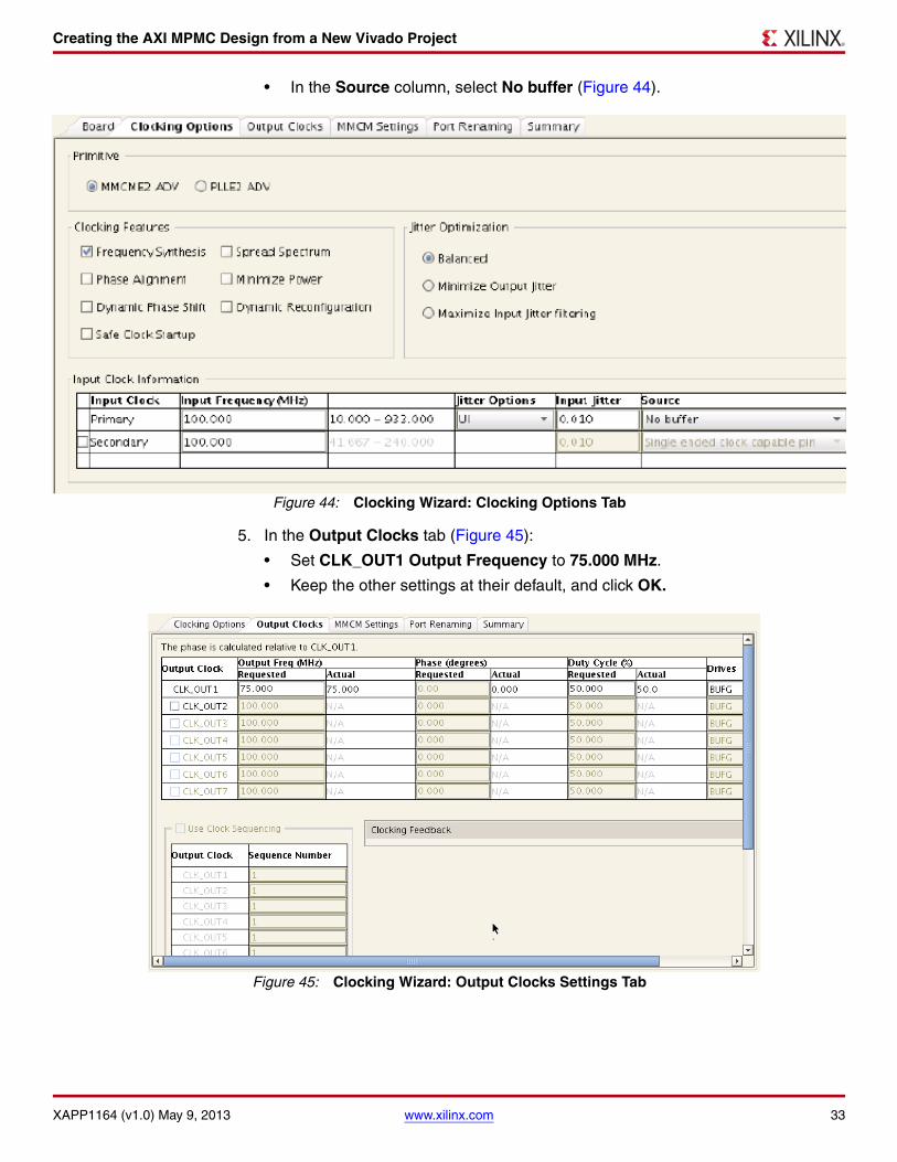
• In the Source column, select No buffer (Figure 44).
5. In the Output Clocks tab (Figure 45):
• Set CLK_OUT1 Output Frequency to 75.000 MHz.
• Keep the other settings at their default, and click OK.
X-Ref Target - Figure 44
Figure 44: Clocking Wizard: Clocking Options Tab
X-Ref Target - Figure 45
Figure 45: Clocking Wizard: Output Clocks Settings Tab

Creating the AXI MPMC Design from a New Vivado Project
XAPP1164 (v1.0) May 9, 2013 www.xilinx.com 34
Adding AXI VDMA to the Design
This section describes the generation of both AXI_VDMA cores into the design. The axi_vdma_1 does the following:
• Receives video data from the master_example core, and places it in DDR3 memory through the write channel.
• Reads data back out, and loops the video data over AXI4-Stream read channels to axi_vdma_2.
The axi_vdma_2 writes the data to memory, and then reads it back out and presents it to the slave_example for display.
Both AXI VDMA cores are configured identically in this design.
1. In the IP integrator diagram, click Add IP.
2. In the IP search, find the AXI Video Direct Memory Access core, and double-click it to add the IP to the diagram (Figure 46).
Configuring VDMA as a Video Frame BufferYou next configure the VDMA to act as a video frame buffer with settings to enable reasonable performance. The following information describes how to configure AXI VDMA.
1. Double-click the axi_vdma_1 block.
2. Duplicate the settings he VDMA Basic tab, as follows:
a. Keep Frame Buffers as 3.
This sets the maximum number of frame buffer ranges needed, and generates associated configuration registers for each. For this design, three frame buffers provides sufficient buffering to allow the MM2S channel to read data, and the channel to write data without the channels overwriting or reading stale data.
X-Ref Target - Figure 46
Figure 46: axi_vdma_1 Block

Creating the AXI MPMC Design from a New Vivado Project
XAPP1164 (v1.0) May 9, 2013 www.xilinx.com 35
b. Enable the Write Channel as follows:- Memory Map Data Width: 32
- Write Burst Size: 256
- Stream Data Width: 32
- Line Buffer Depth: 512
c. Enable the Read Channel as follows:- Memory Map Data Width: 32.
- Write Burst Size: 256
- Stream Data Width: 32
- Line Buffer Depth: 512
This enables the Line Buffers of the VDMA and sets the depth to 512 words.
The line buffers allow some elasticity between the AXI4-Stream and associated AXI4 interfaces providing sufficient buffering to prevent push-back from the VDMA on the AXI4-Stream (Figure 47).
The AXI Interconnect is configured to match the 512 bit x 100 MHz interface of the AXI MIG to which the AXI Interconnect will be connected. This optimizes the performance of the system and reduces the need for width and clock conversion.
X-Ref Target - Figure 47
Figure 47: VDMA Basic Tab

Creating the AXI MPMC Design from a New Vivado Project
XAPP1164 (v1.0) May 9, 2013 www.xilinx.com 36
3. Click the VDMA Advanced tab, ensure that Enable Asynchronous Mode is checked, and configure the settings to match Figure 48, as follows:
a. Write Channel: Fsync options: s2mm fsync
This feature enables the VDMA frame rates to be synchronized to the video endpoint IP to which they are connected.
b. Write Channel: GenLock Mode: Dynamic-Master Gen-Lock is used to maintain frame level synchronization between the read and write channels, thus preventing each interface from overwriting or reading stale data.
c. Read Channel: Fsync Options: mm2s fysnc
d. Read Channel: GenLock Mode: Dynamic Slave 4. Keep all other settings and click OK.
5. In the IP Integrator diagram:
• Select axi_vdma_1, and press Ctrl+C to copy the block.
• Press Ctrl+V to duplicate it as axi_vdma_2, (Figure 49).
X-Ref Target - Figure 48
Figure 48: AXI VDMA Advanced Tab
X-Ref Target - Figure 49
Figure 49: Two VDMA Blocks in Diagram

Creating the AXI MPMC Design from a New Vivado Project
XAPP1164 (v1.0) May 9, 2013 www.xilinx.com 37
Adding Processor System Reset Modules
This subsection describes the generation of both proc_sys_reset cores to the design. The proc_sys_reset_1 generates a reset signal in the MIG 100 MHz clock domain while Proc_sys_reset_2 generates a reset signal in the output of clk_wiz_1 75MHz clock domain.
1. In the IP integrator diagram, click Add IP.
2. Using the Search option, find the Proc Sys Reset core and double-click it to add it to the design.
Figure 50 shows the proc_sys_reset_1 block design.
You can double-click the instance to view the configuration options of the IP; however, the default configuration of the core is used in this design, so no changes are required.
3. Copy (Ctrl+C) proc_sys_reset_1, and then paste (Ctrl+V) the IP block to copy it as proc_sys_reset_2 (Figure 51).
X-Ref Target - Figure 50
Figure 50: proc_reset_1 Block Diagram
X-Ref Target - Figure 51
Figure 51: proc_sys_reset_1 and proc_sys_reset_2 in Block Diagram

Creating the AXI MPMC Design from a New Vivado Project
XAPP1164 (v1.0) May 9, 2013 www.xilinx.com 38
Connecting Modules in the Vivado IDE IP Integrator
This section briefly describes the method of connecting interfaces and signals in the IP integrator block diagram.
Connecting Buses and Wires
1. To make connections between modules, click the port of the module, hold the mouse and drag it to the destination port of another module. If one port has the same type as the source and can be connected with it, there is a green check marked beside the port (Figure 52).
X-Ref Target - Figure 52
Figure 52: Connecting Buses in the Block Diagram

Creating the AXI MPMC Design from a New Vivado Project
XAPP1164 (v1.0) May 9, 2013 www.xilinx.com 39
2. To make connections from one source to multiple destinations, right-click the source port, and select Start Connection Mode, (Figure 53).
3. To connect an I/O port or interface of a module to an external port or interface, right-click the port and select:
• Create Port (for a single I/O port such as init_calib_complete)
• Create Interface Port (for an interface such as DDR3), then click OK (Figure 54).
X-Ref Target - Figure 53
Figure 53: Start Connection Mode from Popup Menu
X-Ref Target - Figure 54
Figure 54: Create Interface Port Option

Creating the AXI MPMC Design from a New Vivado Project
XAPP1164 (v1.0) May 9, 2013 www.xilinx.com 40
Figure 55 shows an external connection in the IP integrator diagram to be used in the design.
You can clean up the diagram and redraw it automatically using the Regenerate button and Zoom buttons (Figure 56).
X-Ref Target - Figure 55
Figure 55: External Connection in IP integrator Diagram
X-Ref Target - Figure 56
Figure 56: Regenerate Button on Design Toolbar

Creating the AXI MPMC Design from a New Vivado Project
XAPP1164 (v1.0) May 9, 2013 www.xilinx.com 41
Setting Clock Properties
The Vivado IDE IP integrator requires frequency information for the output clock ports.
1. To set the clock frequency and the phase for the output port, CLK_OUT1, (Figure 57):
a. Right-click to select External Port Properties.
b. In the External Port Properties window, select the Properties tab. c. Expand the CONFIG property and set FREQ_HZ to 75000000 and PHASE to
0.0. X-Ref Target - Figure 57
Figure 57: Set Frequency for Clock Ports

Creating the AXI MPMC Design from a New Vivado Project
XAPP1164 (v1.0) May 9, 2013 www.xilinx.com 42
External Bus Interface Connection Table
This section lists the bus interfaces which are connected to external ports.
Create the external ports and connect the buses using method described in the IP integrator block diagram, or execute the following Tcl script to complete the same operations.
Bus Connection Table
Table 1 lists the external bus interfaces the internal module name/interface name.
Tcl Script to Create External Interface Port Connectionscreate_bd_intf_port -mode Master -vlnv xilinx.com:interface:ddrx_rtl:1.0 DDR3connect_bd_intf_net [get_bd_intf_ports /DDR3] [get_bd_intf_pins /mig_7series_1/DDR3]create_bd_intf_port -mode Slave -vlnv xilinx.com:interface:aximm_rtl:1.0 S_AXI_LITEconnect_bd_intf_net [get_bd_intf_ports /S_AXI_LITE] [get_bd_intf_pins /axi_vdma_1/S_AXI_LITE]create_bd_intf_port -mode Slave -vlnv xilinx.com:interface:aximm_rtl:1.0 S_AXI_LITE_1connect_bd_intf_net [get_bd_intf_ports /S_AXI_LITE_1] [get_bd_intf_pins /axi_vdma_2/S_AXI_LITE]create_bd_intf_port -mode Slave -vlnv xilinx.com:interface:axis_rtl:1.0 S_AXIS_S2MMconnect_bd_intf_net [get_bd_intf_ports /S_AXIS_S2MM] [get_bd_intf_pins /axi_vdma_1/S_AXIS_S2MM]create_bd_intf_port -mode Master -vlnv xilinx.com:interface:axis_rtl:1.0 M_AXIS_MM2Sconnect_bd_intf_net [get_bd_intf_ports /M_AXIS_MM2S] [get_bd_intf_pins /axi_vdma_2/M_AXIS_MM2S]
Table 2 lists the interface connections.
Tcl Script to Make Connections Between Bus Portsconnect_bd_intf_net [get_bd_intf_pins /axi_vdma_1/M_AXIS_MM2S] [get_bd_intf_pins /axi_vdma_2/S_AXIS_S2MM]connect_bd_intf_net [get_bd_intf_pins /axi_vdma_1/M_AXI_MM2S] [get_bd_intf_pins /axi_interconnect_1/S00_AXI]connect_bd_intf_net [get_bd_intf_pins /axi_vdma_1/M_AXI_S2MM] [get_bd_intf_pins /axi_interconnect_1/S01_AXI]connect_bd_intf_net [get_bd_intf_pins /axi_vdma_2/M_AXI_MM2S] [get_bd_intf_pins /axi_interconnect_1/S02_AXI]connect_bd_intf_net [get_bd_intf_pins /axi_vdma_2/M_AXI_S2MM] [get_bd_intf_pins /axi_interconnect_1/S03_AXI]connect_bd_intf_net [get_bd_intf_pins /axi_interconnect_1/M00_AXI][get_bd_intf_pins /mig_7series_1/S_AXI]
Table 1: External Bus Interface Connections
External Port Name Internal Module Name/Interface Name
DDR3 mig_7series_1/DDR3
S_AXI_LITE axi_vdma_1/S_AXI_LITE
S_AXI_LITE_1 axi_vdma_2/S_AXI_LITE
S_AXIS_S2MM axi_vdma_1/S_AXIS_S2MM
M_AXIS_MM2S axi_vdma_2/M_AXIS_MM2S
Table 2: Interface Connections
Source Module Source Interface Destination Module Destination Interface
axi_vdma_1 M_AXIS_MM2S axi_vdma_2 S_AXIS_S2MM
axi_vdma_1 M_AXI_MM2S axi_interconnect_1 S00_AXI
axi_vdma_1 M_AXI_S2MM; axi_interconnect_1 S01_AXI
axi_vdma_2 M_AXI_MM2S axi_interconnect_1 S02_AXI
axi_vdma_2 M_AXI_S2MM axi_interconnect_1 S03_AXI
axi_interconnect_1 M00_AXI mig_7series_1 S_AXI

Creating the AXI MPMC Design from a New Vivado Project
XAPP1164 (v1.0) May 9, 2013 www.xilinx.com 43
Wire Connection Table
This section lists the wires which are connected in the IP integrator diagram.
Connect the wires using method described in the IP integrator diagram, or execute the following Tcl script to complete the same operations.
Wire Connection Table
Reset Wires Connection Table
Table 3: Clock Wires Connection Table
Source Module Source Wire Destination Module Destination Wire
External Input sys_clk_p mig_7series_1 sys_clk_p
External Input sys_clk_n mig_7series_1 sys_clk_n
mig_7series_1 ui_clk clk_wiz_1 CLK_IN1
mig_7series_1 ui_clk axi_interconnect_1 ACLK
mig_7series_1 ui_clk axi_interconnect_1 M00_ACLK
mig_7series_1 ui_clk proc_sys_reset_1 Slowest_sync_clk
clk_wiz_1 CLK_OUT1 External Output CLK_OUT1
clk_wiz_1 CLK_OUT1 axi_interconnect_1 S00_ACLK
clk_wiz_1 CLK_OUT1 axi_interconnect_1 S01_ACLK
clk_wiz_1 CLK_OUT1 axi_interconnect_1 S02_ACLK
clk_wiz_1 CLK_OUT1 axi_interconnect_1 S03_ACLK
clk_wiz_1 CLK_OUT1 axi_vdma_1 s_axi_lite_aclk
clk_wiz_1 CLK_OUT1 axi_vdma_1 m_axi_mm2s_aclk
clk_wiz_1 CLK_OUT1 axi_vdma_1 m_axis_mm2s_aclk
clk_wiz_1 CLK_OUT1 axi_vdma_1 m_axi_s2mm_aclk
clk_wiz_1 CLK_OUT1 axi_vdma_1 s_axis_s2mm_aclk
clk_wiz_1 CLK_OUT1 axi_vdma_2 s_axi_lite_aclk
clk_wiz_1 CLK_OUT1 axi_vdma_2 m_axi_mm2s_aclk
clk_wiz_1 CLK_OUT1 axi_vdma_2 m_axis_mm2s_aclk
clk_wiz_1 CLK_OUT1 axi_vdma_2 m_axi_s2mm_aclk
clk_wiz_1 CLK_OUT1 axi_vdma_2 s_axis_s2mm_aclk
clk_wiz_1 CLK_OUT1 proc_sys_reset_2 Slowest_sync_clk
Table 4: Reset Wires Connection Table
Source Module Source Wire Destination Module Destination Wire
External Input sys_rst mig_7series_1 sys_rst
mig_7series_1 ui_clk_sync_rst clk_wiz_1 RESET
mig_7series_1 ui_clk_sync_rst proc_sys_reset_1 Ext_Reset_In
mig_7series_1 ui_clk_sync_rst proc_sys_reset_2 Ext_Reset_In
proc_sys_reset_1 Interconnect_aresetn axi_interconnect_1 ARESETN

Creating the AXI MPMC Design from a New Vivado Project
XAPP1164 (v1.0) May 9, 2013 www.xilinx.com 44
General Wires Connection Table
Wire Connection Tcl Scriptcreate_bd_port -dir O init_calib_completeconnect_bd_net [get_bd_ports /init_calib_complete] [get_bd_pins /mig_7series_1/init_calib_complete]create_bd_port -dir I -type rst sys_rstconnect_bd_net [get_bd_ports /sys_rst] [get_bd_pins /mig_7series_1/sys_rst]create_bd_port -dir I -type clk sys_clk_pconnect_bd_net [get_bd_ports /sys_clk_p] [get_bd_pins /mig_7series_1/sys_clk_p]create_bd_port -dir I -type clk sys_clk_nconnect_bd_net [get_bd_ports /sys_clk_n] [get_bd_pins /mig_7series_1/sys_clk_n]
#Next 3 lines were previously performed#create_bd_port -dir O -type clk CLK_OUT1#set_property CONFIG.FREQ_HZ {75000000} [get_bd_ports /CLK_OUT1]#set_property CONFIG.PHASE {0.0} [get_bd_ports /CLK_OUT1]
connect_bd_net [get_bd_ports /CLK_OUT1] [get_bd_pins /clk_wiz_1/CLK_OUT1] [get_bd_pins /axi_vdma_1/s_axi_lite_aclk] [get_bd_pins /axi_vdma_1/m_axi_mm2s_aclk] [get_bd_pins /axi_vdma_1/m_axis_mm2s_aclk] [get_bd_pins /axi_vdma_1/m_axi_s2mm_aclk] [get_bd_pins /axi_vdma_1/s_axis_s2mm_aclk] [get_bd_pins /axi_vdma_2/s_axi_lite_aclk] [get_bd_pins /axi_vdma_2/m_axi_mm2s_aclk] [get_bd_pins /axi_vdma_2/m_axis_mm2s_aclk] [get_bd_pins /axi_vdma_2/m_axi_s2mm_aclk] [get_bd_pins /axi_vdma_2/s_axis_s2mm_aclk] [get_bd_pins /axi_interconnect_1/S00_ACLK] [get_bd_pins /axi_interconnect_1/S01_ACLK] [get_bd_pins /axi_interconnect_1/S02_ACLK] [get_bd_pins /axi_interconnect_1/S03_ACLK] [get_bd_pins /proc_sys_reset_2/Slowest_sync_clk]create_bd_port -dir O -from 0 -to 0 -type rst Peripheral_aresetnconnect_bd_net [get_bd_ports /Peripheral_aresetn] [get_bd_pins /proc_sys_reset_2/Peripheral_aresetn] [get_bd_pins /axi_vdma_1/axi_resetn] [get_bd_pins /axi_vdma_2/axi_resetn]create_bd_port -dir I s2mm_fsyncconnect_bd_net [get_bd_ports /s2mm_fsync] [get_bd_pins /axi_vdma_1/s2mm_fsync]create_bd_port -dir I mm2s_fsyncconnect_bd_net [get_bd_ports /mm2s_fsync] [get_bd_pins /axi_vdma_1/mm2s_fsync] [get_bd_pins /axi_vdma_2/mm2s_fsync] [get_bd_pins /axi_vdma_2/s2mm_fsync]
proc_sys_reset_1 Interconnect_aresetn axi_interconnect_1 M00_ARESETN
proc_sys_reset_2 Interconnect_aresetn axi_interconnect_1 S00_ARESETN
proc_sys_reset_2 Interconnect_aresetn axi_interconnect_1 S01_ARESETN
proc_sys_reset_2 Interconnect_aresetn axi_interconnect_1 S02_ARESETN
proc_sys_reset_2 Interconnect_aresetn axi_interconnect_1 S03_ARESETN
proc_sys_reset_2 Peripheral_aresetn External Output Peripheral_aresetn
proc_sys_reset_2 Peripheral_aresetn axi_vdma_1 axi_resetn
proc_sys_reset_2 Peripheral_aresetn axi_vdma_2 axi_resetn
Table 5: General Wires Connection Table
Source Module Source Wire Destination Module Destination Wire
mig_7series_1 init_calib_complete External Output init_calib_complete
External Input s2mm_fsync axi_vdma_1 s2mm_fsync
External Input mm2s_fsync axi_vdma_1 mm2s_fsync
External Input mm2s_fsync axi_vdma_2 mm2s_fsync
External Input mm2s_fsync axi_vdma_2 s2mm_fsync
clk_wiz_1 LOCKED proc_sys_reset_1 Dcm_locked
clk_wiz_1 LOCKED proc_sys_reset_2 Dcm_locked
Table 4: Reset Wires Connection Table (Cont’d)
Source Module Source Wire Destination Module Destination Wire

Creating the AXI MPMC Design from a New Vivado Project
XAPP1164 (v1.0) May 9, 2013 www.xilinx.com 45
connect_bd_net [get_bd_pins /mig_7series_1/ui_clk_sync_rst] [get_bd_pins /clk_wiz_1/RESET] [get_bd_pins /proc_sys_reset_2/Ext_Reset_In] [get_bd_pins /proc_sys_reset_1/Ext_Reset_In]connect_bd_net [get_bd_pins /mig_7series_1/ui_clk] [get_bd_pins /clk_wiz_1/CLK_IN1] [get_bd_pins /axi_interconnect_1/ACLK] [get_bd_pins /axi_interconnect_1/M00_ACLK] [get_bd_pins /proc_sys_reset_1/Slowest_sync_clk]connect_bd_net [get_bd_pins /proc_sys_reset_1/Interconnect_aresetn] [get_bd_pins /axi_interconnect_1/ARESETN] [get_bd_pins /axi_interconnect_1/M00_ARESETN]connect_bd_net [get_bd_pins /proc_sys_reset_2/Interconnect_aresetn] [get_bd_pins /axi_interconnect_1/S00_ARESETN] [get_bd_pins /axi_interconnect_1/S01_ARESETN] [get_bd_pins /axi_interconnect_1/S02_ARESETN] [get_bd_pins /axi_interconnect_1/S03_ARESETN]connect_bd_net [get_bd_pins /proc_sys_reset_1/Peripheral_aresetn] [get_bd_pins /mig_7series_1/aresetn]connect_bd_net [get_bd_pins /clk_wiz_1/LOCKED] [get_bd_pins /proc_sys_reset_1/Dcm_locked] [get_bd_pins /proc_sys_reset_2/Dcm_locked]
The following additional Tcl commands are needed (or they can be performed by editing the corresponding external wire or interface port properties:
set_property CONFIG.POLARITY {ACTIVE_HIGH} [get_bd_ports /sys_rst]set_property CONFIG.ASSOCIATED_BUSIF {S_AXI_LITE:S_AXI_LITE_1:S_AXIS_S2MM:M_AXIS_MM2S} [get_bd_ports /CLK_OUT1]
Assigning Addresses to the DDR Memory
1. Select the Address Editor tab.
2. Right-click the first entry, axi_vdma_1, and select Auto Assign Address. This maps the 1 GB of DDR3 memory to the address range 0x80000000 to 0xBFFFFFFF and allows the IP integrator tool to configure the address decoders in the AXI Interconnect (Figure 58).
Validating and Saving the Design
The design in the IP integrator tool is complete. Validate the design to check for any errors.
1. Select Tools > Validate, and ensure the message "Validation successful. There are no errors or critical warnings in this design" appears, and click OK.
2. Save the design with File > Save Block Diagram.
X-Ref Target - Figure 58
Figure 58: Auto Assign Address Option

Creating the AXI MPMC Design from a New Vivado Project
XAPP1164 (v1.0) May 9, 2013 www.xilinx.com 46
Figure 59 showns the final IP integrator design.
Adding Other Ready-Made Modules to the Project
Outside of the IP integrator diagram, the user can add custom HDL and connect the custom logic to the IP Integrator subsystem in a higher level HDL file.
Besides the Vivado tool generated IPs for basic building blocks, the system contains some customized logic used to generate test video patterns, configure the DMA engine and display it on the HDMI/DVI display port.
You can add these custom logic blocks as HDL sources or netlists to the project outside of Vivado IDE IP integrator. The following section describes the functions of these modules and the process of adding them to the project.
AXI4-Lite Masters to Configure AXI VDMAs
Each AXI VDMA must be configured at startup to act as a circular frame buffer on 1280x720p video frames. Each AXI VDMA has an AXI4-Lite interface to configure its control registers.
In the system, two, simple write-only AXI4-Lite masters are instantiated.
• Each AXI4-Lite master has an internal state machine that executes a fixed sequence of write commands to properly configure the AXI VDMA blocks.
• A separate AXI4-Lite master IP is connected directly to each AXI VDMA control interface. The AXI4-Lite master design is taken from the sample AXI4-Master design described in Xilinx Answer Record 37425.
X-Ref Target - Figure 59
Figure 59: Final IP Integrator Design Diagram

Creating the AXI MPMC Design from a New Vivado Project
XAPP1164 (v1.0) May 9, 2013 www.xilinx.com 47
AXI4-Stream Test Pattern Generator
The AXI4-Stream source driving AXI VDMA 0 is a video test pattern generator with a Timebase generator (to generate video frame sync signals). The TPG block is delivered as a fixed netlist. The fixed netlist is configured to drive a 1280x720p, 60 hertz video pattern into AXI VDMA 0 using an AXI4-Stream protocol.
AXI4-Stream DVI Display Controller Files
AXI VDMA 1 drives an output AXI4-Stream into a HDMI/DVI display controller with a timebase generator (to generate video frame sync signals).
The DVI display controller block also includes an IIC driver to configure the video chip on the KC705 board. It is delivered as a fixed netlist. The fixed netlist is configured to display a 1280x720p, 60 hertz video signal on the KC705 using an AXI4-Stream protocol from the AXI VDMA 1.
The files related to these modules are in the <design_dir>/src directory. The file names and their functions are listed as follows (Table 6).
Add these files to the project with the following steps:
1. In the Vivado IDE Project Manager, click Project > Add Source > Add or Create Design Sources > Add Files.
2. In the Vivado IDE Source window, browse to the <design_dir>/src/ directory and add the files listed in Table 6.
Table 6: Custom Module File Names
File Name Module File Type
axi_lite_master_vdma_0.v AXI4-Lite Master to Configure AXI VDMAs
Verilog implementation
axi_lite_master_vdma_1.v AXI4-Lite Master to Configure AXI VDMAs
Verilog implementation
axis_master_example.v AXI4-Stream Test Pattern Generator
Netlist-based HDL simulation model and HDL black box definition of the IP
axis_slave_example.v Axi4-Stream DVI Display Controller
Netlist-based HDL simulation model and HDL black box definition of the IP

Creating the AXI MPMC Design from a New Vivado Project
XAPP1164 (v1.0) May 9, 2013 www.xilinx.com 48
3. Click OK (Figure 60).
4. In the Add or Create Design Sources dialog box, confirm the file names and its library and click Finish.
Module Instantiation and System Connection1. In the Design Hierarchy window, go to the Sources tab, right-click the
design_1.bd file, and select Create HDL Wrapper.
This creates design1_wrapper.v, which shows the subsystem instantiation. Normally, the user would then create a top-level HDL file where it instantiates the subsystem and customs cores using the following process sub-steps.
2. To save time, skip to step 3.
a. Create a new top.v file as the top module of the project using the Add Sources dialog box: Add Sources > Add or Create Design Sources > Next > Create File > top.v > OK > Finish > Yes.
b. Copy and paste the IP instantiation template of the IP integrator design, instantiate the remaining custom HDL blocks, and wire them together in top.v.
c. Again, as a time saver, add the completed top-level file, top.v, to integrate all the submodules.
3. From the Project Manager, click Project > Add Source > Add or Create Design Sources > Add Files.
4. In the Add Sources dialog box, browse to <design_dir>/src/top.v, then click OK.
X-Ref Target - Figure 60
Figure 60: Add Source Files Dialog Box

Creating the AXI MPMC Design from a New Vivado Project
XAPP1164 (v1.0) May 9, 2013 www.xilinx.com 49
5. Select the design_1_wrapper.v, then from the popup menu, right-click and select Remove File from Project.
Pinout and Timing Constraints
The design is now completed; however, the design still requires physical constraints for the I/Os and system clock timing constraints.
Pinout constraints can be specified using the Vivado IDE by:
• Synthesizing the design
• Opening the synthesized design and selecting Layout > I/O Planning to display the I/O Planning view (Figure 61). This tool can be used to set location for non-DDR3 related I/O pins.
Note: DDR3 I/O pin location constraints were set in the MIG tool and result in automatically generated core level XDC files associated with the design.
X-Ref Target - Figure 61
Figure 61: I/O Pin Planning Layout

Simulation Testbench
XAPP1164 (v1.0) May 9, 2013 www.xilinx.com 50
This design has only one input clock. All internal clocks are derived from this input clock using the MMCM.
Because the input clock timing constraint was generated by MIG core, and MMCM takes care of all generated clocks. You need only to add the top-level XDC timing constraints for the input clock, and set a false path on the init_calib_complete net, which drives an LED and is not timing sensitive.
The Tcl commands are:
create_clock -period 5.000 -name sys_clk_pin [get_ports sys_clk_p]
set_false_path -through [get_nets init_calib_complete]
To save time, use the completed file <design_dir>/src/constraints/top.xdc, which contains the necessary I/O and timing constraints for the KC705 board.
From the Vivado IDE, select Add Sources > Add or Create Constraints > Add Files > <design_dir>/src/constraints/top.xdc > Finish. (Figure 62).
Simulation Testbench
This design does not support simulation. Because this is a video design with long frame times, simulations of multiple video frames would be impractical.
X-Ref Target - Figure 62
Figure 62: Pin Constraints Added to top.xdc

Equivalent Tcl-Based IP Integrator Design
XAPP1164 (v1.0) May 9, 2013 www.xilinx.com 51
Equivalent Tcl-Based IP Integrator Design
For reference, an equivalent Tcl- based design is implemented. The Tcl script to create the entire Vivado project and all the portions of the design is in <design_dir>/src/tcl/create_design.tcl.
Note: There is an underlying script to build the IP integrator portion of the design at <design_dir>/src/tcl/create_ipi_design.tcl.
To generate the whole project from Tcl, execute the following commands:
1. Create a new empty directory and change to that directory.
2. Open a new Vivado session from the empty directory.
3. In the Tcl Console, type:
source <design_dir>/src/tcl/create_design.tcl
After a few minutes, a new project is created and the AXI MPMC design is created. Then design can then be synthesized, implemented, and a bitstream generated in the GUI, or by running the provided Tcl script.
4. In the Tcl Console, type:
source <design_dir>/src/tcl/generate_design.tcl
Reference Design
Design File Location
The reference design files for this application note can be downloaded at:
https://secure.xilinx.com/webreg/clickthrough.do?cid=333031
Reference Design Checklist
Table 7 is a reference design checklist.
Table 7: Reference Design Checklist
Parameter Description
General
Developer Name Xilinx
Target Devices (Stepping Level, ES, Production, Speed Grades)
Kintex-7 FPGAs
Source Code Provided? Yes (except two blocks delivered as a netlist)
Source Code Format Verilog
Design Uses Code or IP from Existing Reference Design, Application Note, 3rd party, or Vivado Software?
Reference designs provided for flows based on the Vivado tools.
Simulation
Functional Simulation Performed? N/A (simulation not supported)
Timing Simulation Performed? N/A (simulation not supported)
Testbench Provided for Functional and Timing Simulations? N/A (simulation not supported)
Testbench Format N/A (simulation not supported)
Simulator Software and Version N/A (simulation not supported)
SPICE/IBIS Simulations? N/A (simulation not supported)
Implementation

Reference Design
XAPP1164 (v1.0) May 9, 2013 www.xilinx.com 52
Resource Utilization and Clock Frequency
The resource utilization and clock frequency of the system are summarized in Table 8. The system is designed to fit the FPGA resources and speed grade of the XC7K325TFFG900-2 FPGA on the KC705 board. It has not been characterized for other FPGA devices or speed grades.
The AXI MPMC Interconnect and MIG tool are configured for medium to high performance. The system is not area optimized, but is optimized for throughput.
The AXI MPMC portion of the system has more available throughput than the two AXI VDMA masters can consume. The extra available throughput can be used for expansion of the system to include additional AXI4 masters.
See the AXI Reference Guide [Ref 4] for more information about optimizing the AXI MPMC for different area, timing, throughput, latency, and ease of use trade-offs.
Table 9 details the device resource utilization for each IP core.
Note: The information in Table 9 is taken from the Vivado tools by selecting Open Implemented Design and then clicking Implemented Design > Report Utilization (Figure 63, page 53).
Synthesis Software Tools and Version Vivado synthesis 2013.1
Implementation Software Tools and Version Vivado Design Suite 2013.1
Static Timing Analysis Performed? Yes
Hardware Verification
Hardware Verified? Yes
Hardware Platform Used for Verification KC705 Board Rev D
Table 8: Resource Utilization
Parameters Specification/Details
Maximum Frequency (by speed grade) -2 100 MHz (AXI), 400 MHz (Memory Clock)
Device Utilization Slices 12199
LUTs 32894
Registers 33963
GCLK Buffers 3
Block RAMs 58
HDL Language Support Verilog
DDR3 Memory Configuration 64-bit, 400 MHz DDR3 SDRAM
Video Clock Frequency 75 MHz
AXI Interconnect and MIG Main Clocking 100 MHz
Table 7: Reference Design Checklist (Cont’d)
Parameter Description

Reference Design
XAPP1164 (v1.0) May 9, 2013 www.xilinx.com 53
The report shows the resource utilization by resource type and design hierarchy (Figure 64).
Table 9: Module Level Resource Utilization
IP Core Instance Name Slice LUTs
Slice Registers
Block RAMs
MIG mig_7series_1 21208 23072 0
AXI Interconnect axi_interconnect_1 6574 4311 48
VDMA 0 Config axi_lite_master_vdma_0 27 12 0
VDMA 1 Config axi_lite_master_vdma_1 24 9 0
AXI VDMA 0 axi_vdma_1 1718 2276 4
AXI VMDA 1 axi_vdma_2 1709 2260 4
AXI TPG axis_master_example_0 1,037 1,221 2
DVI Controller axis_slave_example_0 586 742 0
Clock Generator clock_generator_1 0 0 0
X-Ref Target - Figure 63
Figure 63: Generating a Resource Utilization Report
X-Ref Target - Figure 64
Figure 64: Obtaining Module Level Resource Utilization

Conclusion
XAPP1164 (v1.0) May 9, 2013 www.xilinx.com 54
The utilization information is approximate due to cross-boundary logic optimizations and logic sharing between modules.
Conclusion This application note describes the steps to build a high-performance AXI MPMC (memory controller and AXI Interconnect) system using the Vivado tools.
It illustrates the steps and design considerations necessary to create a working system in hardware. The AXI MPMC system is exercised by AXI VDMA IP cores moving video frames through DDR3 memory from a video test pattern generator IP block to an HDMI Display IP block. This system can be used as a template and as training information for a new design.
References This document uses the following references:
1. Vivado Design Suite 2013.1 Documentation: http://www.xilinx.com/products/design-tools/vivado/index.htm
2. Advanced Microcontroller Bus Architecture (AMBA) ARM AXI4 specifications http://www.amba.com
3. Kintex-7 FPGA KC705 Evaluation Kit http://www.xilinx.com/products/boards-and-kits/EK-K7-KC705-G.htm
4. UG761, AXI Reference Guide
5. DS768, LogiCORE IP AXI Interconnect Data Sheet
6. UG683, EDK Concepts, Tools, and Techniques: A Hands-On Guide to Effective Embedded System Design
7. UG586, 7 Series FPGAs Memory Interface Solutions User Guide
Revision History
The following table shows the revision history for this document.
Notice of Disclaimer
The information disclosed to you hereunder (the “Materials”) is provided solely for the selection and use ofXilinx products. To the maximum extent permitted by applicable law: (1) Materials are made available "ASIS" and with all faults, Xilinx hereby DISCLAIMS ALL WARRANTIES AND CONDITIONS, EXPRESS,IMPLIED, OR STATUTORY, INCLUDING BUT NOT LIMITED TO WARRANTIES OFMERCHANTABILITY, NON-INFRINGEMENT, OR FITNESS FOR ANY PARTICULAR PURPOSE; and (2)Xilinx shall not be liable (whether in contract or tort, including negligence, or under any other theory ofliability) for any loss or damage of any kind or nature related to, arising under, or in connection with, theMaterials (including your use of the Materials), including for any direct, indirect, special, incidental, orconsequential loss or damage (including loss of data, profits, goodwill, or any type of loss or damagesuffered as a result of any action brought by a third party) even if such damage or loss was reasonablyforeseeable or Xilinx had been advised of the possibility of the same. Xilinx assumes no obligation tocorrect any errors contained in the Materials or to notify you of updates to the Materials or to productspecifications. You may not reproduce, modify, distribute, or publicly display the Materials without priorwritten consent. Certain products are subject to the terms and conditions of the Limited Warranties whichcan be viewed at http://www.xilinx.com/warranty.htm; IP cores may be subject to warranty and supportterms contained in a license issued to you by Xilinx. Xilinx products are not designed or intended to befail-safe or for use in any application requiring fail-safe performance; you assume sole risk and liability foruse of Xilinx products in Critical Applications: http://www.xilinx.com/warranty.htm#critapps.
Date Version Description of Revisions
05/09/13 1.0 Initial Xilinx release.

Automotive Applications Disclaimer
XAPP1164 (v1.0) May 9, 2013 www.xilinx.com 55
Automotive Applications Disclaimer
XILINX PRODUCTS ARE NOT DESIGNED OR INTENDED TO BE FAIL-SAFE, OR FOR USE IN ANY APPLICATION REQUIRING FAIL-SAFE PERFORMANCE, SUCH AS APPLICATIONS RELATED TO: (I) THE DEPLOYMENT OF AIRBAGS, (II) CONTROL OF A VEHICLE, UNLESS THERE IS A FAIL-SAFE OR REDUNDANCY FEATURE (WHICH DOES NOT INCLUDE USE OF SOFTWARE IN THE XILINX DEVICE TO IMPLEMENT THE REDUNDANCY) AND A WARNING SIGNAL UPON FAILURE TO THE OPERATOR, OR (III) USES THAT COULD LEAD TO DEATH OR PERSONAL INJURY. CUSTOMER ASSUMES THE SOLE RISK AND LIABILITY OF ANY USE OF XILINX PRODUCTS IN SUCH APPLICATIONS.


![AXI Protocol Checker v1 - Xilinx · The AXI Protocol Checker core monitors AXI interfaces. When attached to an interface, it ... See ARM AMBA® AXI Protocol v2.0 [Ref 1]. Performance](https://img.pdfslide.net/doc/110x75/5b158bc17f8b9ac7128d1298/axi-protocol-checker-v1-xilinx-the-axi-protocol-checker-core-monitors-axi.jpg)