Embed Size (px)
Citation preview
DS799 June 22, 2011 www.xilinx.com 1Product Specification
© Copyright 2010-2011. Xilinx, Inc. Xilinx, the Xilinx logo, Artix, ISE, Kintex, Spartan, Virtex, Zynq, and other designated brands included herein are trademarks of Xilinx in the United States and other countries. All other trademarks are the property of their respective owners.
IntroductionThe AXI Video Direct Memory Access (AXI VDMA)core is a soft Xilinx IP core for use with the Xilinx®Embedded Development Kit (EDK). The AXI VDMAengine provides high-bandwidth direct memory accessbetween memory and AXI4-Stream-video type targetperipherals. Initialization, status, and managementregisters are accessed through an AXI4-Lite slaveinterface, suitable for the Xilinx MicroBlaze™microprocessor.
Features• AXI4 Compliant
• Primary AXI4 Memory Map data width support of 32, 64, 128, and 256 bits
• Primary AXI4-Stream data width support of 8, 16, 32, 64, 128, and 256 bits
• Optional independent Scatter/Gather DMA support
• Optional register direct mode
• Optional Data Re-Alignment Engine
• Optional Gen-Lock Synchronization
• Optional Line Buffers and Store-And-Forward
• Independent, asynchronous channel operation
LogiCORE IP AXI Video DirectMemory Access (axi_vdma)
(v3.01.a)DS799 June 22, 2011 Product Specification
LogiCORE IP Facts Table
Core Specifics
Supported Device Family(1)
1. For a complete list of supported derivative devices, see IDSEmbedded Edition Derivative Device Support.
Virtex-7, Kintex®-7, Virtex-6, Spartan-6
Supported User Interfaces
AXI4, AXI4-Lite, AXI4-Stream
Resources Frequency
LUTs FFs DSP Slices
Block RAMs Max. Freq.
See Table 41 and Table 42.
Provided with Core
Documentation Product Specification
Design Files VHDL
Example Design Not Provided
Test Bench Not Provided
Constraints File Not Provided
Simulation Model
Not Provided
Tested Design Tools
Design Entry Tools
EDK 13.2 XPS
Simulation(2)
2. For the supported version of the tool, see the ISE Design Suite 13:Release Notes Guide.
QuestaSim-64
Synthesis Tools XST
Support
Provided by Xilinx, Inc.
DS799 June 22, 2011 www.xilinx.com 2Product Specification
LogiCORE IP AXI Video Direct Memory Access (axi_vdma) (v3.01.a)
ApplicationsThe AXI VDMA provides high speed data movement between system memory and AXI4-Stream-based targetVideo IP.
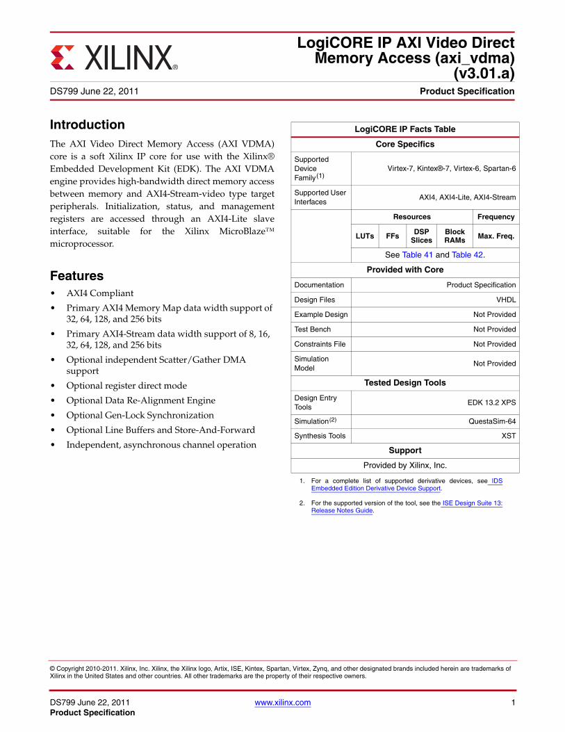
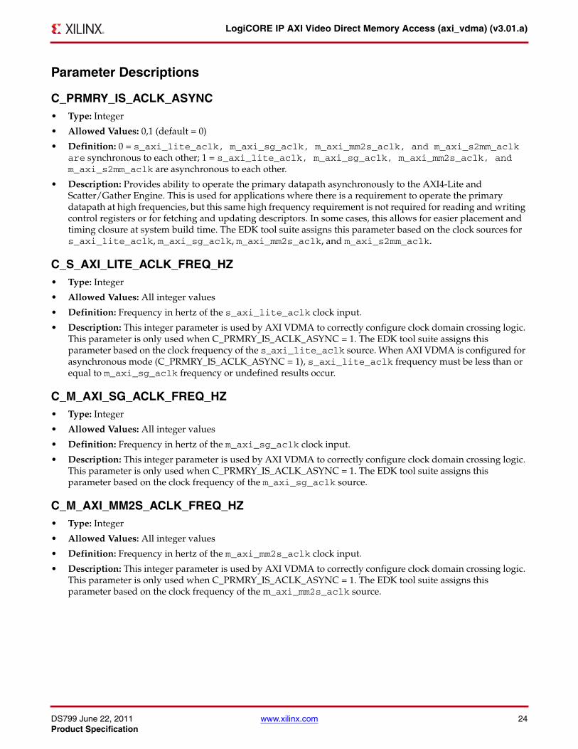
Functional DescriptionFigure 1 illustrates the functional composition of the core when configured for Scatter Gather Mode(C_INCLUDE_SG = 1). The core’s design has four AXI4 Memory Map interfaces: AXI4-Lite Slave, AXI4 MemoryMap Read Master, AXI4 Memory Map Write Master, and AXI4 Memory Map Scatter/Gather Read/Write Master.Associated with the memory map interfaces are two AXI4-Stream interfaces: AXI MM2S Stream Master, AXI S2MMStream Slave.
Optional Gen-Lock and Video Frame Sync Interfaces are also provided for each channel.
Register access and configuration is provided through the AXI4-Lite slave interface. The register module providescontrol and status for DMA operations. X-Ref Target - Figure 1
Figure 1: AXI VDMA Block Diagram (C_INCLUDE_SG = 1)
DS799 June 22, 2011 www.xilinx.com 3Product Specification
LogiCORE IP AXI Video Direct Memory Access (axi_vdma) (v3.01.a)
Primary high-speed DMA data movement between system memory and stream target is through the AXI4 MemoryMap Read Master to AXI MM2S Stream Master, and AXI S2MM Stream Slave to AXI4 Memory Map Write Master.The AXI DataMover is used for high throughput transfer of data from memory to stream and from stream tomemory. The MM2S channel and S2MM channel operate independently and in a full duplex like method. The AXIDataMover provides the AXI VDMA with 4 kbyte address boundary protection, automatic burst partitioning, aswell as providing the ability to queue multiple transfer requests using nearly the full bandwidth capabilities of theAXI4-Stream buses. Furthermore, the AXI DataMover provides byte-level data realignment allowing memoryreads and writes to any byte offset location.
The AXI VDMA provides an Optional Scatter/Gather Engine for offloading CPU management tasks to hardware.The Scatter/Gather Engine fetches and updates buffer descriptors from system memory through the AXI4 MemoryMap Scatter Gather Read/Write Master interface.
DS799 June 22, 2011 www.xilinx.com 4Product Specification
LogiCORE IP AXI Video Direct Memory Access (axi_vdma) (v3.01.a)
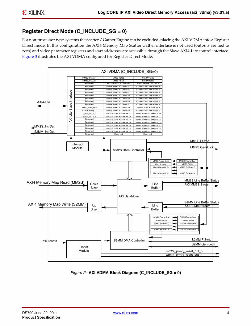
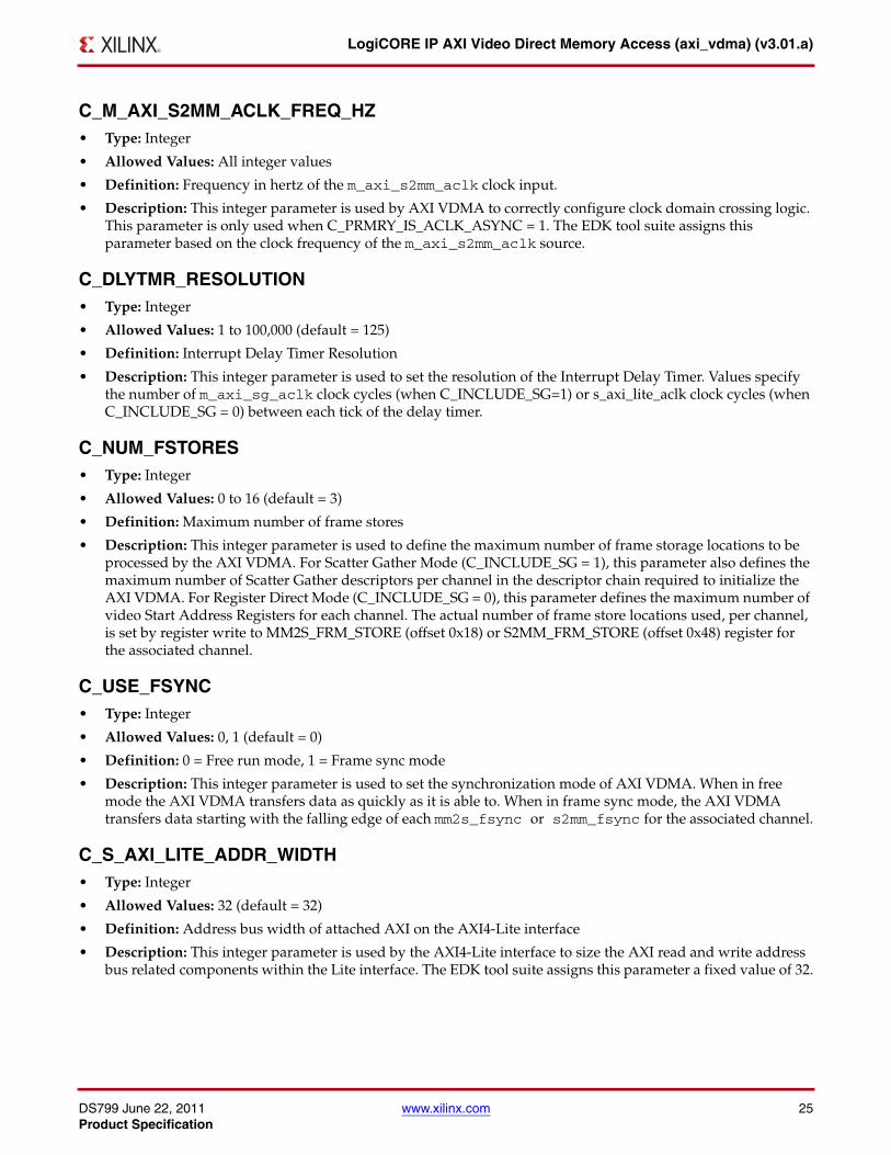
Register Direct Mode (C_INCLUDE_SG = 0)
For non-processor type systems the Scatter / Gather Engine can be excluded, placing the AXI VDMA into a RegisterDirect mode. In this configuration the AXI4 Memory Map Scatter Gather interface is not used (outputs are tied tozero) and video parameter registers and start addresses are accessible through the Slave AXI4-Lite control interface.Figure 3 illustrates the AXI VDMA configured for Register Direct Mode.X-Ref Target - Figure 2
Figure 2: AXI VDMA Block Diagram (C_INCLUDE_SG = 0)
DS799 June 22, 2011 www.xilinx.com 5Product Specification
LogiCORE IP AXI Video Direct Memory Access (axi_vdma) (v3.01.a)
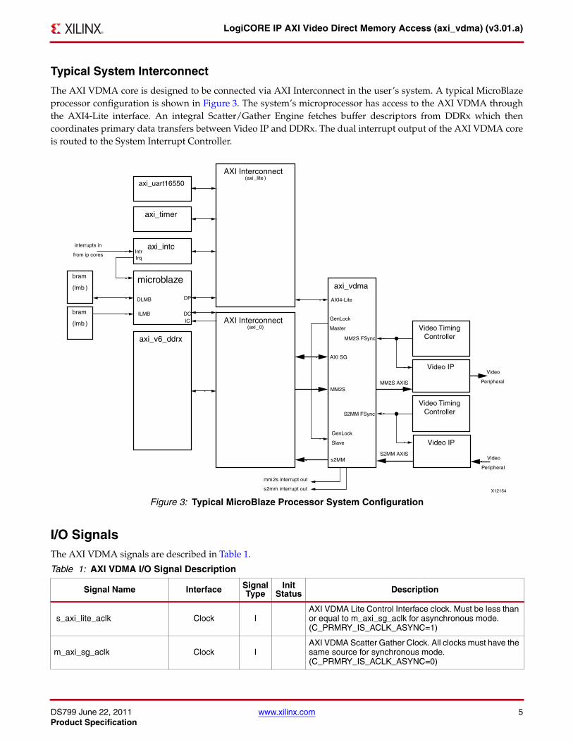
Typical System Interconnect
The AXI VDMA core is designed to be connected via AXI Interconnect in the user’s system. A typical MicroBlazeprocessor configuration is shown in Figure 3. The system’s microprocessor has access to the AXI VDMA throughthe AXI4-Lite interface. An integral Scatter/Gather Engine fetches buffer descriptors from DDRx which thencoordinates primary data transfers between Video IP and DDRx. The dual interrupt output of the AXI VDMA coreis routed to the System Interrupt Controller.
I/O SignalsThe AXI VDMA signals are described in Table 1.
X-Ref Target - Figure 3
Figure 3: Typical MicroBlaze Processor System Configuration
Table 1: AXI VDMA I/O Signal Description
Signal Name Interface SignalType
InitStatus Description
s_axi_lite_aclk Clock IAXI VDMA Lite Control Interface clock. Must be less than or equal to m_axi_sg_aclk for asynchronous mode. (C_PRMRY_IS_ACLK_ASYNC=1)
m_axi_sg_aclk Clock IAXI VDMA Scatter Gather Clock. All clocks must have the same source for synchronous mode. (C_PRMRY_IS_ACLK_ASYNC=0)
DS799 June 22, 2011 www.xilinx.com 6Product Specification
LogiCORE IP AXI Video Direct Memory Access (axi_vdma) (v3.01.a)
m_axi_mm2s_aclk Clock IAXI VDMA MM2S Clock. All clocks must have the same source for synchronous mode. (C_PRMRY_IS_ACLK_ASYNC=0)
m_axi_s2mm_aclk Clock IAXI VDMA S2MM Clock. All clocks must have the same source for synchronous mode. (C_PRMRY_IS_ACLK_ASYNC=0)
axi_resetn Reset I
AXI VDMA Reset. Active low reset. When asserted low, resets entire AXI VDMA core. Must be synchronous to s_axi_lite_aclk and asserted for a minimum 8 clock cycles.
mm2s_introut Interrupt O 0 Interrupt Out for Memory Map to Stream Channel.
s2mm_introut Interrupt O 0 Interrupt Out for Stream to Memory Map Channel.
Video Synchronization Interface
mm2s_fsync Frame Sync I
MM2S Frame Sync Input. When enabled VDMA Operations begin on each falling edge of fsync. This port is only valid when Use Frame Sync is enabled (C_USE_FSYNC=1)
mm2s_fsync_out Frame Sync O 0
MM2S Frame Sync Output. This signal asserts high for 1 axi_mm2s_aclk cycle with each frame boundary. This signals indicates to target video IP when transfer of mms2 new frame data begins.
Note: In free run mode (C_USE_FSYNC = 0) s2mm_fsync_out strobes high when all of the data for a frame as been transferred.
mm2s_prmtr_update Frame Sync O 0
MM2S Parameter Update. This signal indicates new mm2s video parameters take effect on next frame. This signal is asserted for 1 axi_mm2s_aclk cycle coincident with mm2s_fsync_out.
s2mm_fsync Frame Sync I
S2MM Frame Sync Input. When enabled VDMA Operations begin on each falling edge of fsync. This port is only valid when Use Frame Sync is enabled. (C_USE_FSYNC=1)
s2mm_fsync_out Frame Sync O 0
S2MM Frame Sync Output. This signal asserts high for 1 axi_s2mm_aclk cycle with each frame boundary. Indicates when S2MM new frame data can be transferred to the S2MM channel by video IP.
Note: In free run mode (C_USE_FSYNC = 0) s2mm_fsync_out strobes high when all of the data for a frame as been transferred.
s2mm_prmtr_update O 0
S2MM Parameter Update. This signal indicates new s2mm video parameters takes effect on next frame. This signal is asserted for 1 axi_s2mm_aclk cycle coincident with s2mm_fsync_out.
Gen-Lock Interface
mm2s_frame_ptr_in((C_MM2S_GENLOCK_NUM_MASTERS*5)-1: 0)
Gen-Lock IMM2S Frame Pointer Input. In Gen-Lock Slave mode, specifies the next frame for MM2S to operate on.
mm2s_frame_ptr_out(4:0) Gen-Lock O zeros MM2S Frame Pointer Output. In Gen-Lock Master mode, specifies the next frame for the slave VDMA to operate on.
Table 1: AXI VDMA I/O Signal Description (Cont’d)
Signal Name Interface SignalType
InitStatus Description
DS799 June 22, 2011 www.xilinx.com 7Product Specification
LogiCORE IP AXI Video Direct Memory Access (axi_vdma) (v3.01.a)
s2mm_frame_ptr_in((C_S2MM_GENLOCK_NUM_MASTERS*5)-1: 0)
Gen-Lock IS2MM Frame Pointer Input. In Gen-Lock Slave mode, specifies the next frame for S2MM to operate on.
s2mm_frame_ptr_out(4:0) Gen-Lock O zeros S2MM Frame Pointer Output. In Gen-Lock Master mode, specifies the next frame for the slave VDMA to operate on.
Line Buffer interface
mm2s_buffer_empty LineBuffer O 1 MM2S Line Buffer Empty. Indicates the MM2S line buffer contains no stored data elements.
mm2s_buffer_almost_empty LineBuffer O 0
MM2S Line Buffer Almost Empty. Indicates the MM2S line buffer has C_MM2S_LINEBUFFER_THRESH bytes or less stored. When mm2s_buffer_empty asserts mm2s_buffer_almost_empty deasserts.
s2mm_buffer_full LineBuffer O 0 S2MM Line Buffer Full. Indicates the S2MM line buffer as no more room to store data elements
s2mm_buffer_almost_full LineBuffer O 0
S2MM Line Buffer Almost Full. Indicates the S2MM line buffer has C_S2MM_LINEBUFFER_THRESH bytes or more. When s2mm_buffer_full asserts s2mm_buffer_almost_full deasserts.
AXI4-Lite Interface Signals
s_axi_lite_awvalid S_AXI_LITE IAXI4-Lite Write Address Channel Write Address Valid.• 1 = Write address is valid.• 0 = Write address is not valid.
s_axi_lite_awready S_AXI_LITE O 0
AXI4-Lite Write Address Channel Write Address Ready. Indicates DMA ready to accept the write address.• 1 = Ready to accept address.• 0 = Not ready to accept address.
s_axi_lite_awaddr(31:0) S_AXI_LITE I AXI4-Lite Write Address Bus.
s_axi_lite_wvalid S_AXI_LITE IAXI4-Lite Write Data Channel Write Data Valid.• 1 = Write data is valid.• 0 = Write data is not valid.
s_axi_lite_wready S_AXI_LITE O 0
AXI4-Lite Write Data Channel Write Data Ready. Indicates DMA ready to accept the write data.• 1 = Ready to accept data.• 0 = Not ready to accept data.
s_axi_lite_wdata(31:0) S_AXI_LITE I AXI4-Lite Write Data Bus.
s_axi_lite_bresp(1:0) S_AXI_LITE O zeros
AXI4-Lite Write Response Channel. Indicates results of the write transfer. The AXI VDMA Lite interface always responds with OKAY.• 00b = OKAY - Normal access has been successful.• 01b = EXOKAY - Not supported.• 10b = SLVERR - Not supported.• 11b = DECERR - Not supported.
s_axi_lite_bvalid S_AXI_LITE O 0
AXI4-Lite Write Response Channel Response Valid. Indicates response is valid.• 1 = Response is valid.• 0 = Response is not valid.
Table 1: AXI VDMA I/O Signal Description (Cont’d)
Signal Name Interface SignalType
InitStatus Description
DS799 June 22, 2011 www.xilinx.com 8Product Specification
LogiCORE IP AXI Video Direct Memory Access (axi_vdma) (v3.01.a)
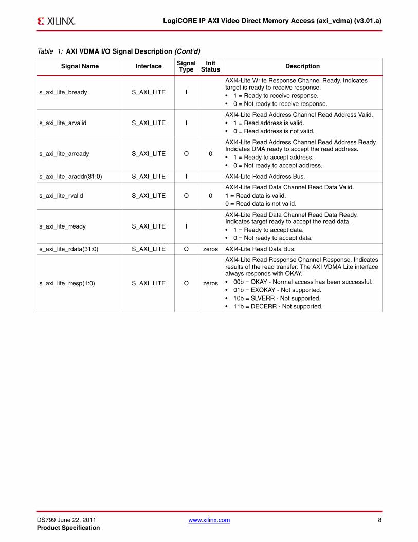
s_axi_lite_bready S_AXI_LITE I
AXI4-Lite Write Response Channel Ready. Indicates target is ready to receive response.• 1 = Ready to receive response.• 0 = Not ready to receive response.
s_axi_lite_arvalid S_AXI_LITE IAXI4-Lite Read Address Channel Read Address Valid.• 1 = Read address is valid.• 0 = Read address is not valid.
s_axi_lite_arready S_AXI_LITE O 0
AXI4-Lite Read Address Channel Read Address Ready. Indicates DMA ready to accept the read address.• 1 = Ready to accept address.• 0 = Not ready to accept address.
s_axi_lite_araddr(31:0) S_AXI_LITE I AXI4-Lite Read Address Bus.
s_axi_lite_rvalid S_AXI_LITE O 0AXI4-Lite Read Data Channel Read Data Valid.1 = Read data is valid.0 = Read data is not valid.
s_axi_lite_rready S_AXI_LITE I
AXI4-Lite Read Data Channel Read Data Ready. Indicates target ready to accept the read data.• 1 = Ready to accept data.• 0 = Not ready to accept data.
s_axi_lite_rdata(31:0) S_AXI_LITE O zeros AXI4-Lite Read Data Bus.
s_axi_lite_rresp(1:0) S_AXI_LITE O zeros
AXI4-Lite Read Response Channel Response. Indicates results of the read transfer. The AXI VDMA Lite interface always responds with OKAY.• 00b = OKAY - Normal access has been successful.• 01b = EXOKAY - Not supported.• 10b = SLVERR - Not supported.• 11b = DECERR - Not supported.
Table 1: AXI VDMA I/O Signal Description (Cont’d)
Signal Name Interface SignalType
InitStatus Description
DS799 June 22, 2011 www.xilinx.com 9Product Specification
LogiCORE IP AXI Video Direct Memory Access (axi_vdma) (v3.01.a)
MM2S Memory Map Read Interface Signals
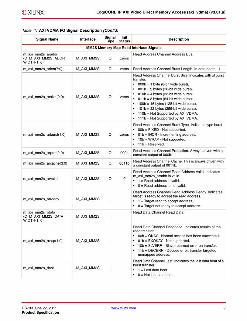
m_axi_mm2s_araddr(C_M_AXI_MM2S_ADDR_WIDTH-1: 0)
M_AXI_MM2S O zerosRead Address Channel Address Bus.
m_axi_mm2s_arlen(7:0) M_AXI_MM2S O zeros Read Address Channel Burst Length. In data beats - 1.
m_axi_mm2s_arsize(2:0) M_AXI_MM2S O zeros
Read Address Channel Burst Size. Indicates with of burst transfer.• 000b = 1 byte (8-bit wide burst).• 001b = 2 bytes (16-bit wide burst).• 010b = 4 bytes (32-bit wide burst).• 011b = 8 bytes (64-bit wide burst).• 100b = 16 bytes (128-bit wide burst).• 101b = 32 bytes (256-bit wide burst).• 110b = Not Supported by AXI VDMA.• 111b = Not Supported by AXI VDMA.
m_axi_mm2s_arburst(1:0) M_AXI_MM2S O zeros
Read Address Channel Burst Type. Indicates type burst.• 00b = FIXED - Not supported.• 01b = INCR - Incrementing address.• 10b = WRAP - Not supported.• 11b = Reserved.
m_axi_mm2s_arprot(2:0) M_AXI_MM2S O 000b Read Address Channel Protection. Always driven with a constant output of 000b.
m_axi_mm2s_arcache(3:0) M_AXI_MM2S O 0011b Read Address Channel Cache. This is always driven with a constant output of 0011b.
m_axi_mm2s_arvalid M_AXI_MM2S O 0
Read Address Channel Read Address Valid. Indicates m_axi_mm2s_araddr is valid.• 1 = Read address is valid.• 0 = Read address is not valid.
m_axi_mm2s_arready M_AXI_MM2S I
Read Address Channel Read Address Ready. Indicates target is ready to accept the read address.• 1 = Target read to accept address.• 0 = Target not ready to accept address.
m_axi_mm2s_rdata(C_M_AXI_MM2S_DATA_WIDTH-1: 0)
M_AXI_MM2S IRead Data Channel Read Data.
m_axi_mm2s_rresp(1:0) M_AXI_MM2S I
Read Data Channel Response. Indicates results of the read transfer.• 00b = OKAY - Normal access has been successful.• 01b = EXOKAY - Not supported.• 10b = SLVERR - Slave returned error on transfer.• 11b = DECERR - Decode error, transfer targeted
unmapped address.
m_axi_mm2s_rlast M_AXI_MM2S I
Read Data Channel Last. Indicates the last data beat of a burst transfer.• 1 = Last data beat.• 0 = Not last data beat.
Table 1: AXI VDMA I/O Signal Description (Cont’d)
Signal Name Interface SignalType
InitStatus Description
DS799 June 22, 2011 www.xilinx.com 10Product Specification
LogiCORE IP AXI Video Direct Memory Access (axi_vdma) (v3.01.a)
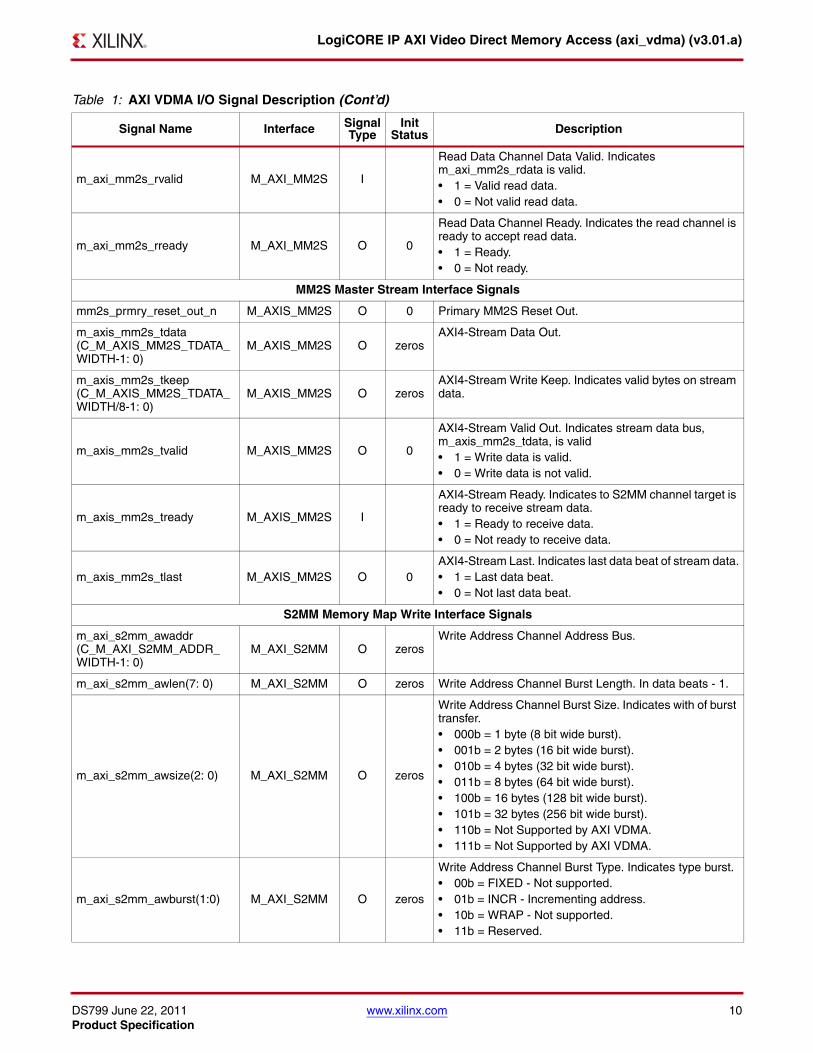
m_axi_mm2s_rvalid M_AXI_MM2S I
Read Data Channel Data Valid. Indicates m_axi_mm2s_rdata is valid.• 1 = Valid read data.• 0 = Not valid read data.
m_axi_mm2s_rready M_AXI_MM2S O 0
Read Data Channel Ready. Indicates the read channel is ready to accept read data.• 1 = Ready.• 0 = Not ready.
MM2S Master Stream Interface Signals
mm2s_prmry_reset_out_n M_AXIS_MM2S O 0 Primary MM2S Reset Out.
m_axis_mm2s_tdata(C_M_AXIS_MM2S_TDATA_WIDTH-1: 0)
M_AXIS_MM2S O zerosAXI4-Stream Data Out.
m_axis_mm2s_tkeep(C_M_AXIS_MM2S_TDATA_WIDTH/8-1: 0)
M_AXIS_MM2S O zerosAXI4-Stream Write Keep. Indicates valid bytes on stream data.
m_axis_mm2s_tvalid M_AXIS_MM2S O 0
AXI4-Stream Valid Out. Indicates stream data bus, m_axis_mm2s_tdata, is valid• 1 = Write data is valid.• 0 = Write data is not valid.
m_axis_mm2s_tready M_AXIS_MM2S I
AXI4-Stream Ready. Indicates to S2MM channel target is ready to receive stream data.• 1 = Ready to receive data.• 0 = Not ready to receive data.
m_axis_mm2s_tlast M_AXIS_MM2S O 0AXI4-Stream Last. Indicates last data beat of stream data.• 1 = Last data beat.• 0 = Not last data beat.
S2MM Memory Map Write Interface Signals
m_axi_s2mm_awaddr(C_M_AXI_S2MM_ADDR_WIDTH-1: 0)
M_AXI_S2MM O zerosWrite Address Channel Address Bus.
m_axi_s2mm_awlen(7: 0) M_AXI_S2MM O zeros Write Address Channel Burst Length. In data beats - 1.
m_axi_s2mm_awsize(2: 0) M_AXI_S2MM O zeros
Write Address Channel Burst Size. Indicates with of burst transfer.• 000b = 1 byte (8 bit wide burst).• 001b = 2 bytes (16 bit wide burst).• 010b = 4 bytes (32 bit wide burst).• 011b = 8 bytes (64 bit wide burst).• 100b = 16 bytes (128 bit wide burst).• 101b = 32 bytes (256 bit wide burst).• 110b = Not Supported by AXI VDMA.• 111b = Not Supported by AXI VDMA.
m_axi_s2mm_awburst(1:0) M_AXI_S2MM O zeros
Write Address Channel Burst Type. Indicates type burst.• 00b = FIXED - Not supported.• 01b = INCR - Incrementing address.• 10b = WRAP - Not supported.• 11b = Reserved.
Table 1: AXI VDMA I/O Signal Description (Cont’d)
Signal Name Interface SignalType
InitStatus Description
DS799 June 22, 2011 www.xilinx.com 11Product Specification
LogiCORE IP AXI Video Direct Memory Access (axi_vdma) (v3.01.a)
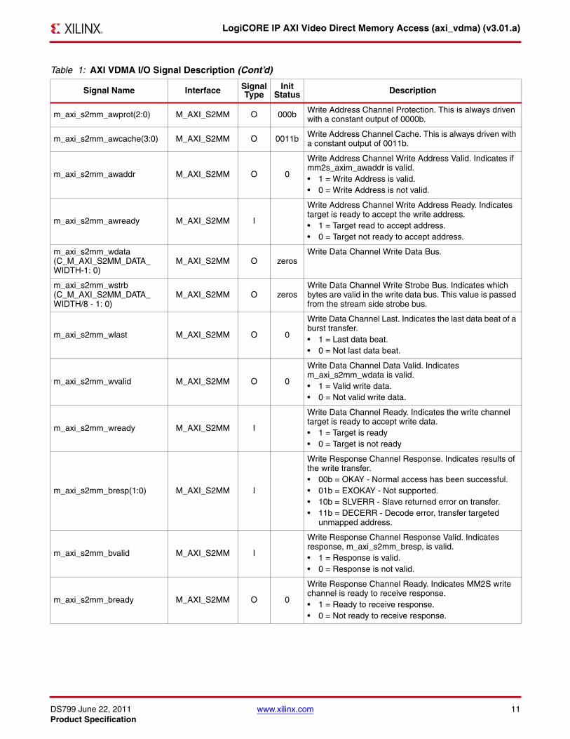
m_axi_s2mm_awprot(2:0) M_AXI_S2MM O 000b Write Address Channel Protection. This is always driven with a constant output of 0000b.
m_axi_s2mm_awcache(3:0) M_AXI_S2MM O 0011b Write Address Channel Cache. This is always driven with a constant output of 0011b.
m_axi_s2mm_awaddr M_AXI_S2MM O 0
Write Address Channel Write Address Valid. Indicates if mm2s_axim_awaddr is valid.• 1 = Write Address is valid.• 0 = Write Address is not valid.
m_axi_s2mm_awready M_AXI_S2MM I
Write Address Channel Write Address Ready. Indicates target is ready to accept the write address.• 1 = Target read to accept address.• 0 = Target not ready to accept address.
m_axi_s2mm_wdata(C_M_AXI_S2MM_DATA_WIDTH-1: 0)
M_AXI_S2MM O zerosWrite Data Channel Write Data Bus.
m_axi_s2mm_wstrb(C_M_AXI_S2MM_DATA_WIDTH/8 - 1: 0)
M_AXI_S2MM O zerosWrite Data Channel Write Strobe Bus. Indicates which bytes are valid in the write data bus. This value is passed from the stream side strobe bus.
m_axi_s2mm_wlast M_AXI_S2MM O 0
Write Data Channel Last. Indicates the last data beat of a burst transfer.• 1 = Last data beat.• 0 = Not last data beat.
m_axi_s2mm_wvalid M_AXI_S2MM O 0
Write Data Channel Data Valid. Indicates m_axi_s2mm_wdata is valid.• 1 = Valid write data.• 0 = Not valid write data.
m_axi_s2mm_wready M_AXI_S2MM I
Write Data Channel Ready. Indicates the write channel target is ready to accept write data.• 1 = Target is ready• 0 = Target is not ready
m_axi_s2mm_bresp(1:0) M_AXI_S2MM I
Write Response Channel Response. Indicates results of the write transfer.• 00b = OKAY - Normal access has been successful.• 01b = EXOKAY - Not supported.• 10b = SLVERR - Slave returned error on transfer.• 11b = DECERR - Decode error, transfer targeted
unmapped address.
m_axi_s2mm_bvalid M_AXI_S2MM I
Write Response Channel Response Valid. Indicates response, m_axi_s2mm_bresp, is valid.• 1 = Response is valid.• 0 = Response is not valid.
m_axi_s2mm_bready M_AXI_S2MM O 0
Write Response Channel Ready. Indicates MM2S write channel is ready to receive response.• 1 = Ready to receive response.• 0 = Not ready to receive response.
Table 1: AXI VDMA I/O Signal Description (Cont’d)
Signal Name Interface SignalType
InitStatus Description
DS799 June 22, 2011 www.xilinx.com 12Product Specification
LogiCORE IP AXI Video Direct Memory Access (axi_vdma) (v3.01.a)
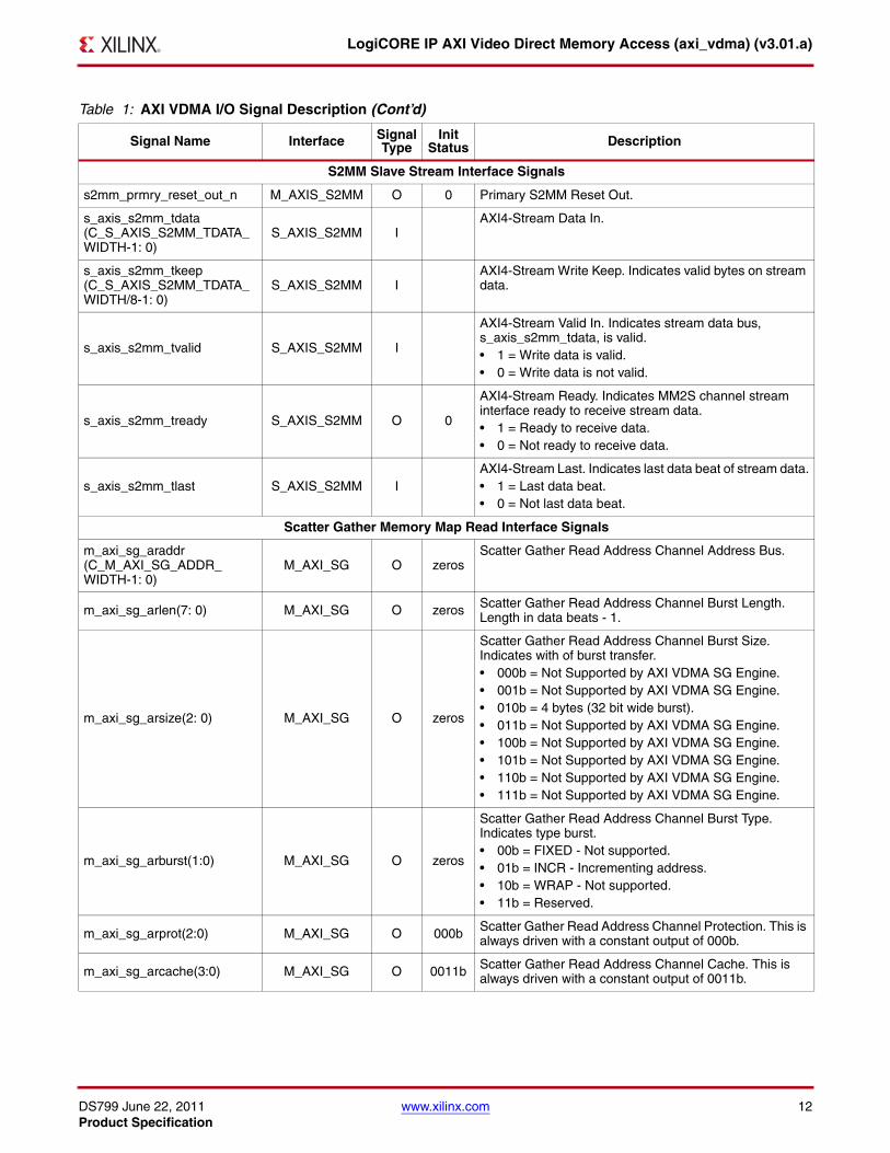
S2MM Slave Stream Interface Signals
s2mm_prmry_reset_out_n M_AXIS_S2MM O 0 Primary S2MM Reset Out.
s_axis_s2mm_tdata(C_S_AXIS_S2MM_TDATA_WIDTH-1: 0)
S_AXIS_S2MM IAXI4-Stream Data In.
s_axis_s2mm_tkeep(C_S_AXIS_S2MM_TDATA_WIDTH/8-1: 0)
S_AXIS_S2MM IAXI4-Stream Write Keep. Indicates valid bytes on stream data.
s_axis_s2mm_tvalid S_AXIS_S2MM I
AXI4-Stream Valid In. Indicates stream data bus, s_axis_s2mm_tdata, is valid.• 1 = Write data is valid.• 0 = Write data is not valid.
s_axis_s2mm_tready S_AXIS_S2MM O 0
AXI4-Stream Ready. Indicates MM2S channel stream interface ready to receive stream data.• 1 = Ready to receive data.• 0 = Not ready to receive data.
s_axis_s2mm_tlast S_AXIS_S2MM IAXI4-Stream Last. Indicates last data beat of stream data.• 1 = Last data beat.• 0 = Not last data beat.
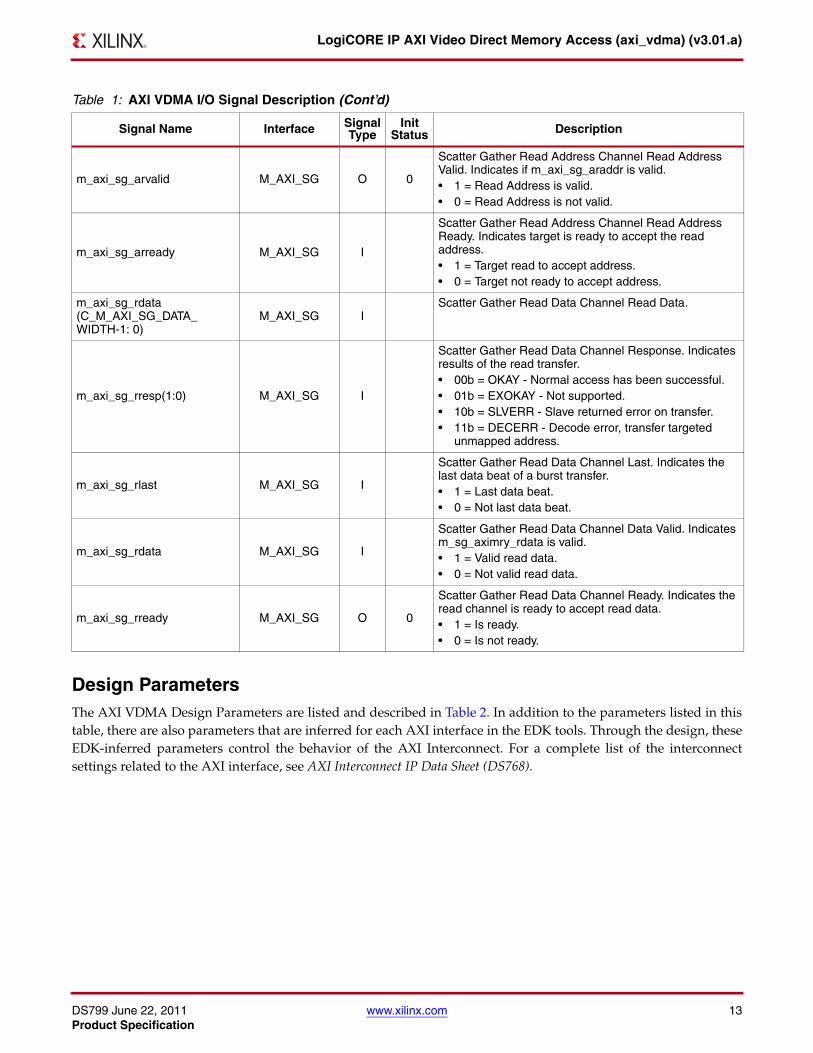
Scatter Gather Memory Map Read Interface Signals
m_axi_sg_araddr(C_M_AXI_SG_ADDR_WIDTH-1: 0)
M_AXI_SG O zerosScatter Gather Read Address Channel Address Bus.
m_axi_sg_arlen(7: 0) M_AXI_SG O zeros Scatter Gather Read Address Channel Burst Length. Length in data beats - 1.
m_axi_sg_arsize(2: 0) M_AXI_SG O zeros
Scatter Gather Read Address Channel Burst Size. Indicates with of burst transfer.• 000b = Not Supported by AXI VDMA SG Engine.• 001b = Not Supported by AXI VDMA SG Engine.• 010b = 4 bytes (32 bit wide burst).• 011b = Not Supported by AXI VDMA SG Engine.• 100b = Not Supported by AXI VDMA SG Engine.• 101b = Not Supported by AXI VDMA SG Engine.• 110b = Not Supported by AXI VDMA SG Engine.• 111b = Not Supported by AXI VDMA SG Engine.
m_axi_sg_arburst(1:0) M_AXI_SG O zeros
Scatter Gather Read Address Channel Burst Type. Indicates type burst.• 00b = FIXED - Not supported.• 01b = INCR - Incrementing address.• 10b = WRAP - Not supported.• 11b = Reserved.
m_axi_sg_arprot(2:0) M_AXI_SG O 000b Scatter Gather Read Address Channel Protection. This is always driven with a constant output of 000b.
m_axi_sg_arcache(3:0) M_AXI_SG O 0011b Scatter Gather Read Address Channel Cache. This is always driven with a constant output of 0011b.
Table 1: AXI VDMA I/O Signal Description (Cont’d)
Signal Name Interface SignalType
InitStatus Description
DS799 June 22, 2011 www.xilinx.com 13Product Specification
LogiCORE IP AXI Video Direct Memory Access (axi_vdma) (v3.01.a)
Design ParametersThe AXI VDMA Design Parameters are listed and described in Table 2. In addition to the parameters listed in thistable, there are also parameters that are inferred for each AXI interface in the EDK tools. Through the design, theseEDK-inferred parameters control the behavior of the AXI Interconnect. For a complete list of the interconnectsettings related to the AXI interface, see AXI Interconnect IP Data Sheet (DS768).
m_axi_sg_arvalid M_AXI_SG O 0
Scatter Gather Read Address Channel Read Address Valid. Indicates if m_axi_sg_araddr is valid.• 1 = Read Address is valid.• 0 = Read Address is not valid.
m_axi_sg_arready M_AXI_SG I
Scatter Gather Read Address Channel Read Address Ready. Indicates target is ready to accept the read address.• 1 = Target read to accept address.• 0 = Target not ready to accept address.
m_axi_sg_rdata(C_M_AXI_SG_DATA_WIDTH-1: 0)
M_AXI_SG IScatter Gather Read Data Channel Read Data.
m_axi_sg_rresp(1:0) M_AXI_SG I
Scatter Gather Read Data Channel Response. Indicates results of the read transfer.• 00b = OKAY - Normal access has been successful.• 01b = EXOKAY - Not supported.• 10b = SLVERR - Slave returned error on transfer.• 11b = DECERR - Decode error, transfer targeted
unmapped address.
m_axi_sg_rlast M_AXI_SG I
Scatter Gather Read Data Channel Last. Indicates the last data beat of a burst transfer.• 1 = Last data beat.• 0 = Not last data beat.
m_axi_sg_rdata M_AXI_SG I
Scatter Gather Read Data Channel Data Valid. Indicates m_sg_aximry_rdata is valid.• 1 = Valid read data.• 0 = Not valid read data.
m_axi_sg_rready M_AXI_SG O 0
Scatter Gather Read Data Channel Ready. Indicates the read channel is ready to accept read data.• 1 = Is ready.• 0 = Is not ready.
Table 1: AXI VDMA I/O Signal Description (Cont’d)
Signal Name Interface SignalType
InitStatus Description
DS799 June 22, 2011 www.xilinx.com 14Product Specification
LogiCORE IP AXI Video Direct Memory Access (axi_vdma) (v3.01.a)
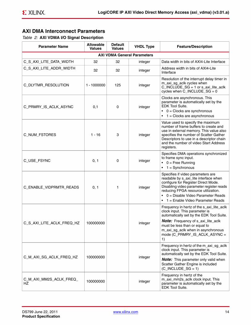
AXI DMA Interconnect ParametersTable 2: AXI VDMA I/O Signal Description
Parameter Name Allowable Values
Default Values VHDL Type Feature/Description
AXI VDMA General Parameters
C_S_AXI_LITE_DATA_WIDTH 32 32 integer Data width in bits of AXI4-Lite Interface
C_S_AXI_LITE_ADDR_WIDTH 32 32 integer Address width in bits of AXI4-Lite Interface
C_DLYTMR_RESOLUTION 1 - 1000000 125 integer
Resolution of the interrupt delay timer in m_axi_sg_aclk cycles when C_INCLUDE_SG = 1 or s_axi_lite_aclk cycles when C_INCLUDE_SG = 0
C_PRMRY_IS_ACLK_ASYNC 0,1 0 integer
Clocks are asynchronous. This parameter is automatically set by the EDK Tool Suite.• 0 = Clocks are synchronous• 1 = Clocks are asynchronous
C_NUM_FSTORES 1 - 16 3 integer
Value used to specify the maximum number of frame buffers to create and use in external memory. This value also specifies the number of Scatter Gather Descriptors to use in a descriptor chain and the number of video Start Address registers.
C_USE_FSYNC 0, 1 0 integer
Specifies DMA operations synchronized to frame sync input.• 0 = Free Running• 1 = Synchronous
C_ENABLE_VIDPRMTR_READS 0, 1 1 integer
Specifies if video parameters are readable by s_axi_lite interface when configure for Register Direct Mode. Disabling video parameter register reads reducing FPGA resource utilization.• 0 = Disable Video Parameter Reads• 1 = Enable Video Parameter Reads
C_S_AXI_LITE_ACLK_FREQ_HZ 100000000 integer
Frequency in hertz of the s_axi_lite_aclk clock input. This parameter is automatically set by the EDK Tool Suite.
Note: Frequency of s_axi_lite_aclk must be less than or equal to m_axi_sg_aclk when in asynchronous mode (C_PRMRY_IS_ACLK_ASYNC = 1)
C_M_AXI_SG_ACLK_FREQ_HZ 100000000 integer
Frequency in hertz of the m_axi_sg_aclk clock input. This parameter is automatically set by the EDK Tool Suite.
Note: This parameter only valid when Scatter Gather Engine is included (C_INCLUDE_SG = 1)
C_M_AXI_MM2S_ACLK_FREQ_HZ 100000000 integer
Frequency in hertz of the m_axi_mm2s_aclk clock input. This parameter is automatically set by the EDK Tool Suite.
DS799 June 22, 2011 www.xilinx.com 15Product Specification
LogiCORE IP AXI Video Direct Memory Access (axi_vdma) (v3.01.a)
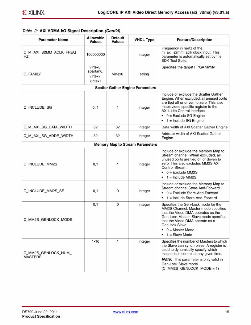
C_M_AXI_S2MM_ACLK_FREQ_HZ 100000000 integer
Frequency in hertz of the m_axi_s2mm_aclk clock input. This parameter is automatically set by the EDK Tool Suite.
C_FAMILY
virtex6, spartan6,virtex7,kintex7
virtex6 string
Specifies the target FPGA family
Scatter Gather Engine Parameters
C_INCLUDE_SG 0, 1 1 integer
Include or exclude the Scatter Gather Engine. When excluded, all unused ports are tied off or driven to zero. This also maps video specific register to the AXI4-Lite Control interface.• 0 = Exclude SG Engine• 1 = Include SG Engine
C_M_AXI_SG_DATA_WIDTH 32 32 integer Data width of AXI Scatter Gather Engine
C_M_AXI_SG_ADDR_WIDTH 32 32 integer Address width of AXI Scatter Gather Engine
Memory Map to Stream Parameters
C_INCLUDE_MM2S 0,1 1 integer
Include or exclude the Memory Map to Stream channel. When excluded, all unused ports are tied off or driven to zero. This also excludes MM2S AXI Control Stream.• 0 = Exclude MM2S• 1 = Include MM2S
C_INCLUDE_MM2S_SF 0,1 0 integer
Include or exclude the Memory Map to Stream channel Store-And-Forward.• 0 = Exclude Store-And-Forward• 1 = Include Store-And-Forward
C_MM2S_GENLOCK_MODE
0,1 0 integer Specifies the Gen-Lock mode for the MM2S Channel. Master mode specifies that the Video DMA operates as the Gen-Lock Master. Slave mode specifies that the Video DMA operate as a Gen-lock Slave.• 0 = Master Mode• 1 = Slave Mode
C_MM2S_GENLOCK_NUM_MASTERS
1-16 1 integer Specifies the number of Masters to which the Slave can synchronize. A register is used to dynamically specify which master is in control at any given time.
Note: This parameter is only valid in Gen-Lock Slave mode (C_MM2S_GENLOCK_MODE = 1)
Table 2: AXI VDMA I/O Signal Description (Cont’d)
Parameter Name Allowable Values
Default Values VHDL Type Feature/Description
DS799 June 22, 2011 www.xilinx.com 16Product Specification
LogiCORE IP AXI Video Direct Memory Access (axi_vdma) (v3.01.a)
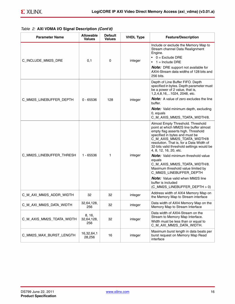
C_INCLUDE_MM2S_DRE 0,1 0 integer
Include or exclude the Memory Map to Stream channel Data Realignment Engine.• 0 = Exclude DRE• 1 = Include DRE
Note: DRE support not available for AXI4-Stream data widths of 128 bits and 256 bits.
C_MM2S_LINEBUFFER_DEPTH 0 - 65536 128 integer
Depth of Line Buffer FIFO. Depth specified in bytes. Depth parameter must be a power of 2 value, that is, 1,2,4,8,16,...1024, 2048, etc.
Note: A value of zero excludes the line buffer.
Note: Valid minimum depth, excluding 0, equals C_M_AXIS_MM2S_TDATA_WIDTH/8.
C_MM2S_LINEBUFFER_THRESH 1 - 65536 1 integer
Almost Empty Threshold. Threshold point at which MM2S line buffer almost empty flag asserts high. Threshold specified in bytes and must be C_M_AXIS_MM2S_TDATA_WIDTH/8 resolution. That is, for a Data Width of 32-bits valid threshold settings would be 4, 8, 12, 16, 20, etc.
Note: Valid minimum threshold value equals C_M_AXIS_MM2S_TDATA_WIDTH/8. Maximum threshold value limited by C_MM2S_LINEBUFFER_DEPTH
Note: Value valid when MM2S line buffer is included (C_MM2S_LINEBUFFER_DEPTH > 0)
C_M_AXI_MM2S_ADDR_WIDTH 32 32 integer Address width of AXI4 Memory Map on the Memory Map to Stream interface
C_M_AXI_MM2S_DATA_WIDTH 32,64,128,256 32 integer Data width of AXI4 Memory Map on the
Memory Map to Stream Interface
C_M_AXIS_MM2S_TDATA_WIDTH8, 16,
32,64,128,256
32 integer
Data width of AXI4-Stream on the Stream to Memory Map Interface. Width must be less than or equal to C_M_AXI_MM2S_DATA_WIDTH.
C_MM2S_MAX_BURST_LENGTH 16,32,64,128,256 16 integer
Maximum burst length in data beats per burst request on Memory Map Read interface
Table 2: AXI VDMA I/O Signal Description (Cont’d)
Parameter Name Allowable Values
Default Values VHDL Type Feature/Description
DS799 June 22, 2011 www.xilinx.com 17Product Specification
LogiCORE IP AXI Video Direct Memory Access (axi_vdma) (v3.01.a)
Stream to Memory Map Parameters
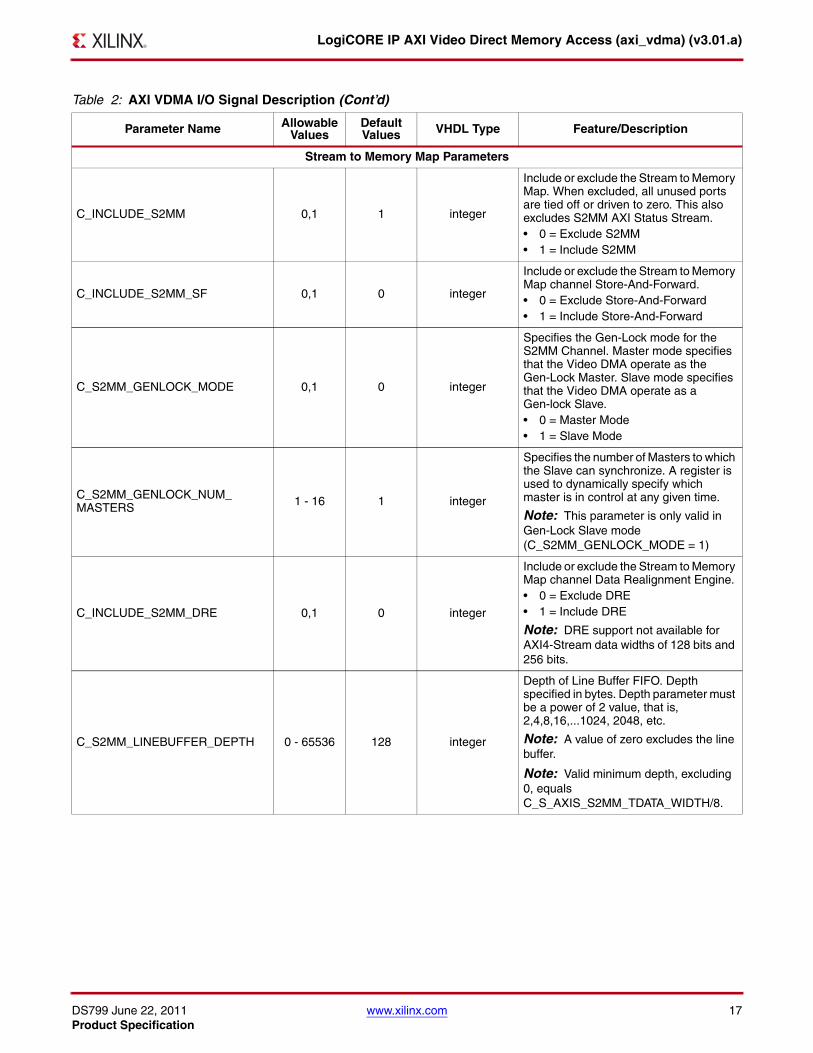
C_INCLUDE_S2MM 0,1 1 integer
Include or exclude the Stream to Memory Map. When excluded, all unused ports are tied off or driven to zero. This also excludes S2MM AXI Status Stream.• 0 = Exclude S2MM• 1 = Include S2MM
C_INCLUDE_S2MM_SF 0,1 0 integer
Include or exclude the Stream to Memory Map channel Store-And-Forward.• 0 = Exclude Store-And-Forward• 1 = Include Store-And-Forward
C_S2MM_GENLOCK_MODE 0,1 0 integer
Specifies the Gen-Lock mode for the S2MM Channel. Master mode specifies that the Video DMA operate as the Gen-Lock Master. Slave mode specifies that the Video DMA operate as a Gen-lock Slave. • 0 = Master Mode• 1 = Slave Mode
C_S2MM_GENLOCK_NUM_MASTERS 1 - 16 1 integer
Specifies the number of Masters to which the Slave can synchronize. A register is used to dynamically specify which master is in control at any given time.
Note: This parameter is only valid in Gen-Lock Slave mode (C_S2MM_GENLOCK_MODE = 1)
C_INCLUDE_S2MM_DRE 0,1 0 integer
Include or exclude the Stream to Memory Map channel Data Realignment Engine.• 0 = Exclude DRE• 1 = Include DRE
Note: DRE support not available for AXI4-Stream data widths of 128 bits and 256 bits.
C_S2MM_LINEBUFFER_DEPTH 0 - 65536 128 integer
Depth of Line Buffer FIFO. Depth specified in bytes. Depth parameter must be a power of 2 value, that is, 2,4,8,16,...1024, 2048, etc.
Note: A value of zero excludes the line buffer.
Note: Valid minimum depth, excluding 0, equals C_S_AXIS_S2MM_TDATA_WIDTH/8.
Table 2: AXI VDMA I/O Signal Description (Cont’d)
Parameter Name Allowable Values
Default Values VHDL Type Feature/Description
DS799 June 22, 2011 www.xilinx.com 18Product Specification
LogiCORE IP AXI Video Direct Memory Access (axi_vdma) (v3.01.a)
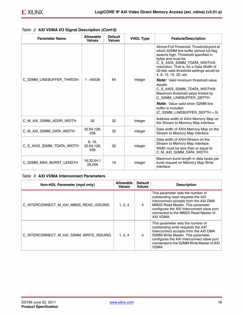
C_S2MM_LINEBUFFER_THRESH 1 - 65536 64 integer
Almost Full Threshold. Threshold point at which S2MM line buffer almost full flag asserts high. Threshold specified in bytes and must be C_S_AXIS_S2MM_TDATA_WIDTH/8 resolution. That is, for a Data Width of 32-bits valid threshold settings would be 4, 8, 12, 16, 20, etc.
Note: Valid minimum threshold value equals C_S_AXIS_S2MM_TDATA_WIDTH/8. Maximum threshold value limited by C_S2MM_LINEBUFFER_DEPTH
Note: Value valid when S2MM line buffer is included (C_S2MM_LINEBUFFER_DEPTH > 0)
C_M_AXI_S2MM_ADDR_WIDTH 32 32 integer Address width of AXI4 Memory Map on the Stream to Memory Map interface
C_M_AXI_S2MM_DATA_WIDTH 32,64,128,256 32 integer Data width of AXI4 Memory Map on the
Stream to Memory Map Interface
C_S_AXIS_S2MM_TDATA_WIDTH8, 16,
32,64,128,256
32 integer
Data width of AXI4-Stream on the Stream to Memory Map Interface. Width must be less than or equal to C_M_AXI_S2MM_DATA_WIDTH.
C_S2MM_MAX_BURST_LENGTH 16,32,64,128,256 16 integer
Maximum burst length in data beats per burst request on Memory Map Write interface
Table 3: AXI VDMA Interconnect Parameters
Non-HDL Parameter (mpd only) Allowable Values
DefaultValues Description
C_INTERCONNECT_M_AXI_MM2S_READ_ISSUING 1, 2, 4 4
This parameter sets the number of outstanding read requests the AXI Interconnect accepts from the AXI DMA MM2S Read Master. This parameter configures the AXI Interconnect slave port connected to the MM2S Read Master of AXI VDMA.
C_INTERCONNECT_M_AXI_S2MM_WRITE_ISSUING 1, 2, 4 4
This parameter sets the number of outstanding write requests the AXI Interconnect accepts from the AXI DMA S2MM Write Master. This parameter configures the AXI Interconnect slave port connected to the S2MM Write Master of AXI VDMA.
Table 2: AXI VDMA I/O Signal Description (Cont’d)
Parameter Name Allowable Values
Default Values VHDL Type Feature/Description
DS799 June 22, 2011 www.xilinx.com 19Product Specification
LogiCORE IP AXI Video Direct Memory Access (axi_vdma) (v3.01.a)
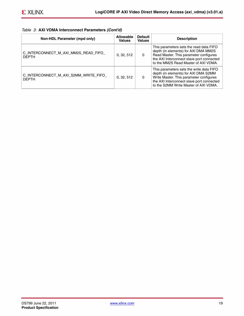
C_INTERCONNECT_M_AXI_MM2S_READ_FIFO_DEPTH 0, 32, 512 0
This parameters sets the read data FIFO depth (in elements) for AXI DMA MM2S Read Master. This parameter configures the AXI Interconnect slave port connected to the MM2S Read Master of AXI VDMA.
C_INTERCONNECT_M_AXI_S2MM_WRITE_FIFO_DEPTH 0, 32, 512 0
This parameters sets the write data FIFO depth (in elements) for AXI DMA S2MM Write Master. This parameter configures the AXI Interconnect slave port connected to the S2MM Write Master of AXI VDMA.
Table 3: AXI VDMA Interconnect Parameters (Cont’d)
Non-HDL Parameter (mpd only) Allowable Values
DefaultValues Description
DS799 June 22, 2011 www.xilinx.com 20Product Specification
LogiCORE IP AXI Video Direct Memory Access (axi_vdma) (v3.01.a)
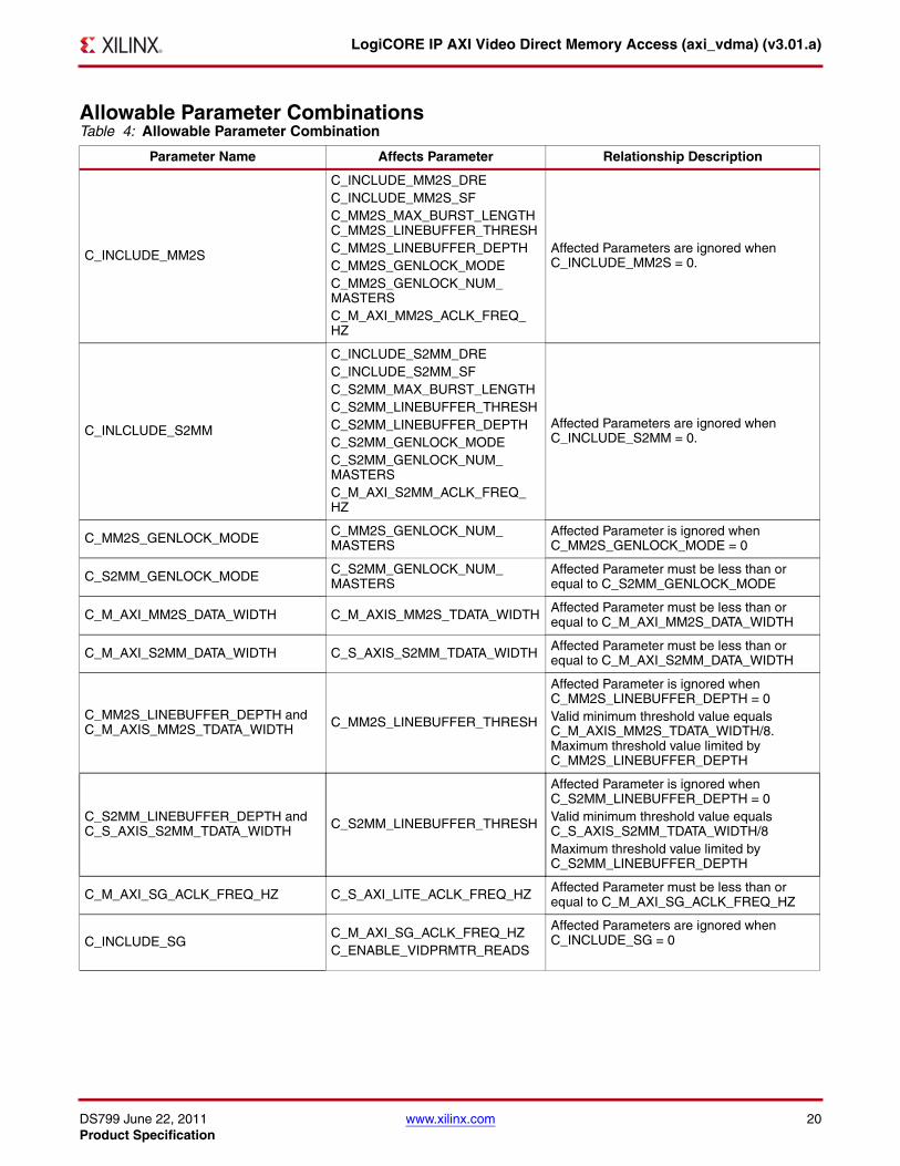
Allowable Parameter CombinationsTable 4: Allowable Parameter Combination
Parameter Name Affects Parameter Relationship Description
C_INCLUDE_MM2S
C_INCLUDE_MM2S_DREC_INCLUDE_MM2S_SFC_MM2S_MAX_BURST_LENGTHC_MM2S_LINEBUFFER_THRESHC_MM2S_LINEBUFFER_DEPTHC_MM2S_GENLOCK_MODEC_MM2S_GENLOCK_NUM_MASTERSC_M_AXI_MM2S_ACLK_FREQ_HZ
Affected Parameters are ignored when C_INCLUDE_MM2S = 0.
C_INLCLUDE_S2MM
C_INCLUDE_S2MM_DREC_INCLUDE_S2MM_SFC_S2MM_MAX_BURST_LENGTHC_S2MM_LINEBUFFER_THRESHC_S2MM_LINEBUFFER_DEPTHC_S2MM_GENLOCK_MODEC_S2MM_GENLOCK_NUM_MASTERSC_M_AXI_S2MM_ACLK_FREQ_HZ
Affected Parameters are ignored when C_INCLUDE_S2MM = 0.
C_MM2S_GENLOCK_MODE C_MM2S_GENLOCK_NUM_MASTERS
Affected Parameter is ignored when C_MM2S_GENLOCK_MODE = 0
C_S2MM_GENLOCK_MODE C_S2MM_GENLOCK_NUM_MASTERS
Affected Parameter must be less than or equal to C_S2MM_GENLOCK_MODE
C_M_AXI_MM2S_DATA_WIDTH C_M_AXIS_MM2S_TDATA_WIDTH Affected Parameter must be less than or equal to C_M_AXI_MM2S_DATA_WIDTH
C_M_AXI_S2MM_DATA_WIDTH C_S_AXIS_S2MM_TDATA_WIDTH Affected Parameter must be less than or equal to C_M_AXI_S2MM_DATA_WIDTH
C_MM2S_LINEBUFFER_DEPTH and C_M_AXIS_MM2S_TDATA_WIDTH C_MM2S_LINEBUFFER_THRESH
Affected Parameter is ignored when C_MM2S_LINEBUFFER_DEPTH = 0Valid minimum threshold value equals C_M_AXIS_MM2S_TDATA_WIDTH/8. Maximum threshold value limited by C_MM2S_LINEBUFFER_DEPTH
C_S2MM_LINEBUFFER_DEPTH and C_S_AXIS_S2MM_TDATA_WIDTH C_S2MM_LINEBUFFER_THRESH
Affected Parameter is ignored when C_S2MM_LINEBUFFER_DEPTH = 0Valid minimum threshold value equals C_S_AXIS_S2MM_TDATA_WIDTH/8Maximum threshold value limited by C_S2MM_LINEBUFFER_DEPTH
C_M_AXI_SG_ACLK_FREQ_HZ C_S_AXI_LITE_ACLK_FREQ_HZ Affected Parameter must be less than or equal to C_M_AXI_SG_ACLK_FREQ_HZ
C_INCLUDE_SGC_M_AXI_SG_ACLK_FREQ_HZC_ENABLE_VIDPRMTR_READS
Affected Parameters are ignored when C_INCLUDE_SG = 0
DS799 June 22, 2011 www.xilinx.com 21Product Specification
LogiCORE IP AXI Video Direct Memory Access (axi_vdma) (v3.01.a)
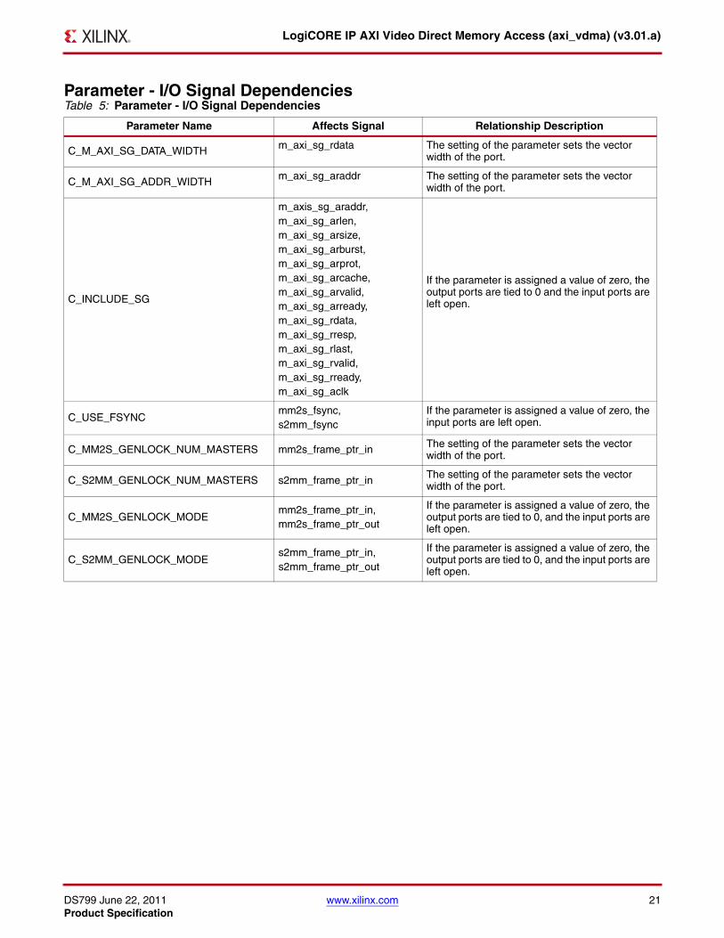
Parameter - I/O Signal DependenciesTable 5: Parameter - I/O Signal Dependencies
Parameter Name Affects Signal Relationship Description
C_M_AXI_SG_DATA_WIDTH m_axi_sg_rdata The setting of the parameter sets the vector width of the port.
C_M_AXI_SG_ADDR_WIDTH m_axi_sg_araddr The setting of the parameter sets the vector width of the port.
C_INCLUDE_SG
m_axis_sg_araddr,m_axi_sg_arlen,m_axi_sg_arsize,m_axi_sg_arburst,m_axi_sg_arprot,m_axi_sg_arcache,m_axi_sg_arvalid,m_axi_sg_arready,m_axi_sg_rdata,m_axi_sg_rresp,m_axi_sg_rlast,m_axi_sg_rvalid,m_axi_sg_rready,m_axi_sg_aclk
If the parameter is assigned a value of zero, the output ports are tied to 0 and the input ports are left open.
C_USE_FSYNCmm2s_fsync,s2mm_fsync
If the parameter is assigned a value of zero, the input ports are left open.
C_MM2S_GENLOCK_NUM_MASTERS mm2s_frame_ptr_in The setting of the parameter sets the vector width of the port.
C_S2MM_GENLOCK_NUM_MASTERS s2mm_frame_ptr_in The setting of the parameter sets the vector width of the port.
C_MM2S_GENLOCK_MODEmm2s_frame_ptr_in,mm2s_frame_ptr_out
If the parameter is assigned a value of zero, the output ports are tied to 0, and the input ports are left open.
C_S2MM_GENLOCK_MODEs2mm_frame_ptr_in,s2mm_frame_ptr_out
If the parameter is assigned a value of zero, the output ports are tied to 0, and the input ports are left open.
DS799 June 22, 2011 www.xilinx.com 22Product Specification
LogiCORE IP AXI Video Direct Memory Access (axi_vdma) (v3.01.a)
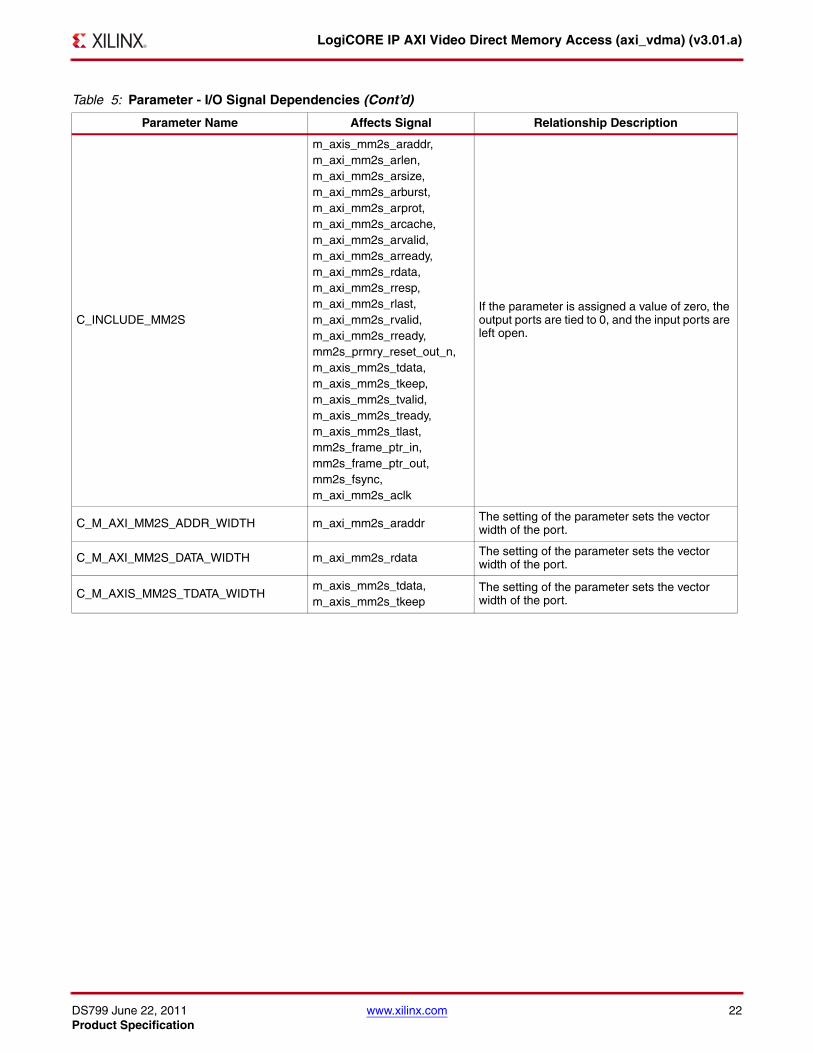
C_INCLUDE_MM2S
m_axis_mm2s_araddr,m_axi_mm2s_arlen,m_axi_mm2s_arsize,m_axi_mm2s_arburst,m_axi_mm2s_arprot,m_axi_mm2s_arcache,m_axi_mm2s_arvalid,m_axi_mm2s_arready,m_axi_mm2s_rdata,m_axi_mm2s_rresp,m_axi_mm2s_rlast,m_axi_mm2s_rvalid,m_axi_mm2s_rready,mm2s_prmry_reset_out_n,m_axis_mm2s_tdata,m_axis_mm2s_tkeep,m_axis_mm2s_tvalid,m_axis_mm2s_tready,m_axis_mm2s_tlast,mm2s_frame_ptr_in,mm2s_frame_ptr_out,mm2s_fsync,m_axi_mm2s_aclk
If the parameter is assigned a value of zero, the output ports are tied to 0, and the input ports are left open.
C_M_AXI_MM2S_ADDR_WIDTH m_axi_mm2s_araddr The setting of the parameter sets the vector width of the port.
C_M_AXI_MM2S_DATA_WIDTH m_axi_mm2s_rdata The setting of the parameter sets the vector width of the port.
C_M_AXIS_MM2S_TDATA_WIDTHm_axis_mm2s_tdata,m_axis_mm2s_tkeep
The setting of the parameter sets the vector width of the port.
Table 5: Parameter - I/O Signal Dependencies (Cont’d)
Parameter Name Affects Signal Relationship Description
DS799 June 22, 2011 www.xilinx.com 23Product Specification
LogiCORE IP AXI Video Direct Memory Access (axi_vdma) (v3.01.a)
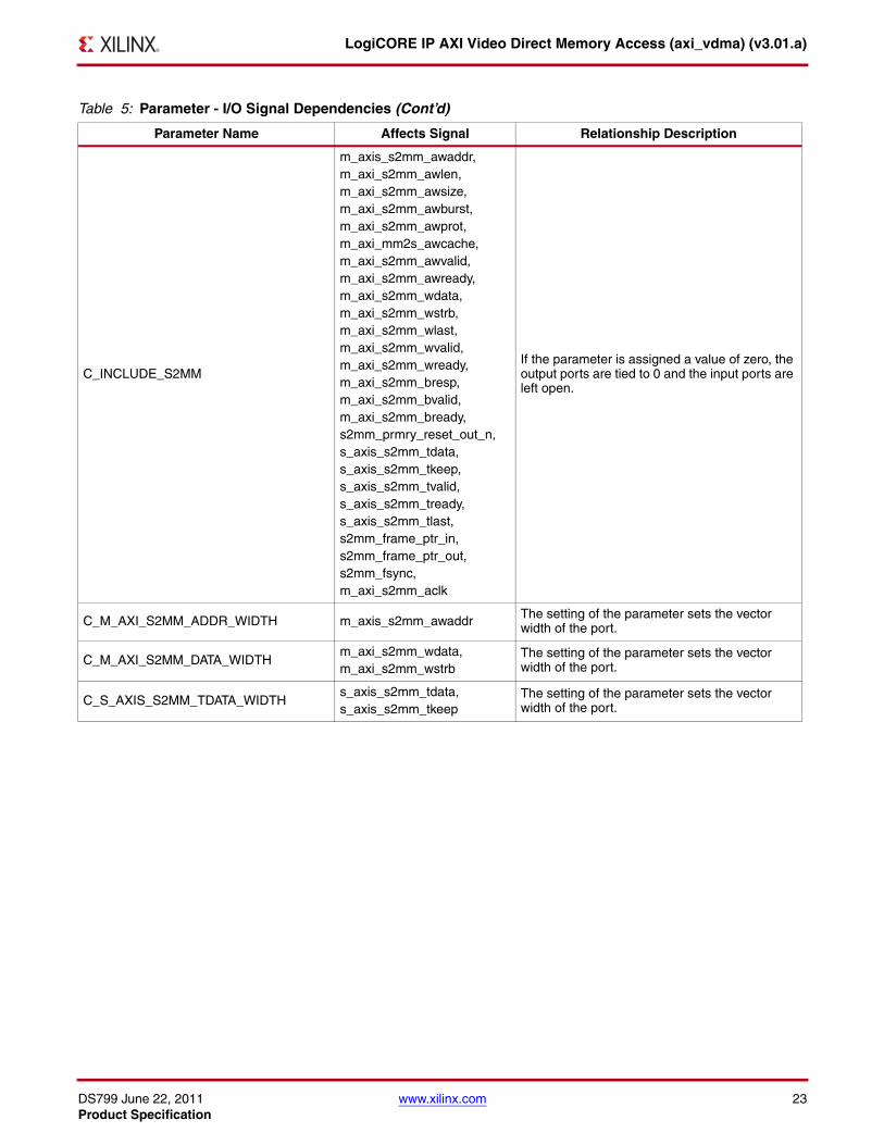
C_INCLUDE_S2MM
m_axis_s2mm_awaddr,m_axi_s2mm_awlen,m_axi_s2mm_awsize,m_axi_s2mm_awburst,m_axi_s2mm_awprot,m_axi_mm2s_awcache,m_axi_s2mm_awvalid,m_axi_s2mm_awready,m_axi_s2mm_wdata,m_axi_s2mm_wstrb,m_axi_s2mm_wlast,m_axi_s2mm_wvalid,m_axi_s2mm_wready,m_axi_s2mm_bresp,m_axi_s2mm_bvalid,m_axi_s2mm_bready,s2mm_prmry_reset_out_n,s_axis_s2mm_tdata,s_axis_s2mm_tkeep,s_axis_s2mm_tvalid,s_axis_s2mm_tready,s_axis_s2mm_tlast,s2mm_frame_ptr_in,s2mm_frame_ptr_out,s2mm_fsync,m_axi_s2mm_aclk
If the parameter is assigned a value of zero, the output ports are tied to 0 and the input ports are left open.
C_M_AXI_S2MM_ADDR_WIDTH m_axis_s2mm_awaddr The setting of the parameter sets the vector width of the port.
C_M_AXI_S2MM_DATA_WIDTHm_axi_s2mm_wdata,m_axi_s2mm_wstrb
The setting of the parameter sets the vector width of the port.
C_S_AXIS_S2MM_TDATA_WIDTHs_axis_s2mm_tdata,s_axis_s2mm_tkeep
The setting of the parameter sets the vector width of the port.
Table 5: Parameter - I/O Signal Dependencies (Cont’d)
Parameter Name Affects Signal Relationship Description
DS799 June 22, 2011 www.xilinx.com 24Product Specification
LogiCORE IP AXI Video Direct Memory Access (axi_vdma) (v3.01.a)
Parameter Descriptions
C_PRMRY_IS_ACLK_ASYNC• Type: Integer
• Allowed Values: 0,1 (default = 0)
• Definition: 0 = s_axi_lite_aclk, m_axi_sg_aclk, m_axi_mm2s_aclk, and m_axi_s2mm_aclk are synchronous to each other; 1 = s_axi_lite_aclk, m_axi_sg_aclk, m_axi_mm2s_aclk, and m_axi_s2mm_aclk are asynchronous to each other.
• Description: Provides ability to operate the primary datapath asynchronously to the AXI4-Lite and Scatter/Gather Engine. This is used for applications where there is a requirement to operate the primary datapath at high frequencies, but this same high frequency requirement is not required for reading and writing control registers or for fetching and updating descriptors. In some cases, this allows for easier placement and timing closure at system build time. The EDK tool suite assigns this parameter based on the clock sources for s_axi_lite_aclk, m_axi_sg_aclk, m_axi_mm2s_aclk, and m_axi_s2mm_aclk.
C_S_AXI_LITE_ACLK_FREQ_HZ• Type: Integer
• Allowed Values: All integer values
• Definition: Frequency in hertz of the s_axi_lite_aclk clock input.
• Description: This integer parameter is used by AXI VDMA to correctly configure clock domain crossing logic. This parameter is only used when C_PRMRY_IS_ACLK_ASYNC = 1. The EDK tool suite assigns this parameter based on the clock frequency of the s_axi_lite_aclk source. When AXI VDMA is configured for asynchronous mode (C_PRMRY_IS_ACLK_ASYNC = 1), s_axi_lite_aclk frequency must be less than or equal to m_axi_sg_aclk frequency or undefined results occur.
C_M_AXI_SG_ACLK_FREQ_HZ• Type: Integer
• Allowed Values: All integer values
• Definition: Frequency in hertz of the m_axi_sg_aclk clock input.
• Description: This integer parameter is used by AXI VDMA to correctly configure clock domain crossing logic. This parameter is only used when C_PRMRY_IS_ACLK_ASYNC = 1. The EDK tool suite assigns this parameter based on the clock frequency of the m_axi_sg_aclk source.
C_M_AXI_MM2S_ACLK_FREQ_HZ• Type: Integer
• Allowed Values: All integer values
• Definition: Frequency in hertz of the m_axi_mm2s_aclk clock input.
• Description: This integer parameter is used by AXI VDMA to correctly configure clock domain crossing logic. This parameter is only used when C_PRMRY_IS_ACLK_ASYNC = 1. The EDK tool suite assigns this parameter based on the clock frequency of the m_axi_mm2s_aclk source.
DS799 June 22, 2011 www.xilinx.com 25Product Specification
LogiCORE IP AXI Video Direct Memory Access (axi_vdma) (v3.01.a)
C_M_AXI_S2MM_ACLK_FREQ_HZ• Type: Integer
• Allowed Values: All integer values
• Definition: Frequency in hertz of the m_axi_s2mm_aclk clock input.
• Description: This integer parameter is used by AXI VDMA to correctly configure clock domain crossing logic. This parameter is only used when C_PRMRY_IS_ACLK_ASYNC = 1. The EDK tool suite assigns this parameter based on the clock frequency of the m_axi_s2mm_aclk source.
C_DLYTMR_RESOLUTION• Type: Integer
• Allowed Values: 1 to 100,000 (default = 125)
• Definition: Interrupt Delay Timer Resolution
• Description: This integer parameter is used to set the resolution of the Interrupt Delay Timer. Values specify the number of m_axi_sg_aclk clock cycles (when C_INCLUDE_SG=1) or s_axi_lite_aclk clock cycles (when C_INCLUDE_SG = 0) between each tick of the delay timer.
C_NUM_FSTORES• Type: Integer
• Allowed Values: 0 to 16 (default = 3)
• Definition: Maximum number of frame stores
• Description: This integer parameter is used to define the maximum number of frame storage locations to be processed by the AXI VDMA. For Scatter Gather Mode (C_INCLUDE_SG = 1), this parameter also defines the maximum number of Scatter Gather descriptors per channel in the descriptor chain required to initialize the AXI VDMA. For Register Direct Mode (C_INCLUDE_SG = 0), this parameter defines the maximum number of video Start Address Registers for each channel. The actual number of frame store locations used, per channel, is set by register write to MM2S_FRM_STORE (offset 0x18) or S2MM_FRM_STORE (offset 0x48) register for the associated channel.
C_USE_FSYNC• Type: Integer
• Allowed Values: 0, 1 (default = 0)
• Definition: 0 = Free run mode, 1 = Frame sync mode
• Description: This integer parameter is used to set the synchronization mode of AXI VDMA. When in free mode the AXI VDMA transfers data as quickly as it is able to. When in frame sync mode, the AXI VDMA transfers data starting with the falling edge of each mm2s_fsync or s2mm_fsync for the associated channel.
C_S_AXI_LITE_ADDR_WIDTH• Type: Integer
• Allowed Values: 32 (default = 32)
• Definition: Address bus width of attached AXI on the AXI4-Lite interface
• Description: This integer parameter is used by the AXI4-Lite interface to size the AXI read and write address bus related components within the Lite interface. The EDK tool suite assigns this parameter a fixed value of 32.
DS799 June 22, 2011 www.xilinx.com 26Product Specification
LogiCORE IP AXI Video Direct Memory Access (axi_vdma) (v3.01.a)
C_S_AXI_LITE_DATA_WIDTH• Type: Integer
• Allowed Values: 32 (default = 32)
• Definition: Data bus width of attached AXI on the AXI4-Lite interface
• Description: This integer parameter is used by the AXI4-Lite interface to size the AXI read and write data bus related components within the Lite interface. The EDK tool suite assigns this parameter a fixed value of 32.
C_INCLUDE_SG• Type: Integer
• Allowed Values: 0,1 (default = 1)
• Definition: 0 = Exclude SG Engine; 1 = Include SG Engine
• Description: Include or exclude Scatter / Gather Engine. Setting this parameter to 0 causes all output ports for the Scatter/Gather engine to be tied to zero, and all of the input ports to be left open. Excluding the Scatter/Gather engine configures the AXI VDMA for Register Direct Mode.
C_M_AXI_SG_DATA_WIDTH• Type: Integer
• Allowed Values: 32 (default = 32)
• Definition: Data bus width of attached AXI on the AXI Scatter/Gather interface
• Description: This integer parameter is used by the AXI Scatter/Gather interface to size the AXI read data bus related components within the Scatter/Gather Engine. The EDK tool suite assigns this parameter a fixed value of 32.
C_M_AXI_SG_ADDR_WIDTH• Type: Integer
• Allowed Values: 32 (default = 32)
• Definition: Address bus width of attached AXI on the AXI Scatter Gather interface
• Description: This integer parameter is used by the AXI Scatter Gather interface to size the AXI read address bus related components within the Scatter Gather Engine. The EDK tool suite assigns this parameter a fixed value of 32.
C_INCLUDE_MM2S• Type: Integer
• Allowed Values: 0,1 (default = 1)
• Definition: 0 = Exclude MM2S Channel; 1 = Include MM2S Channel
• Description: Include or exclude MM2S Channel. Setting this parameter to 0 causes all output ports for the MM2S channel to be tied to zero, and all of the input ports for the respective channel to be left open.
Note: Setting both C_INCLUDE_MM2S = 0 and C_INCLUDE_S2MM = 0 disables all logic within the AXI VDMA and is not a valid configuration.
DS799 June 22, 2011 www.xilinx.com 27Product Specification
LogiCORE IP AXI Video Direct Memory Access (axi_vdma) (v3.01.a)
C_INCLUDE_S2MM• Type: Integer
• Allowed Values: 0,1 (default = 1)
• Definition: 0 = Exclude S2MM Channel; 1 = Include S2MM Channel
• Description: Include or exclude S2MM Channel. Setting this parameter to 0 causes all output ports for the S2MM channel to be tied to zero, and all of the input ports for the respective channel to be left open.
Note: Setting both C_INCLUDE_MM2S = 0 and C_INCLUDE_S2MM = 0 disables all logic within the AXI VDMA and is not a valid configuration.
C_INCLUDE_MM2S_DRE• Type: Integer
• Allowed Values: 0,1 (default = 0)
• Definition: 0 = Exclude MM2S Data Realignment Engine; 1 = Include MM2S Data Realignment Engine
• Description: Include or exclude MM2S Data Realignment Engine. For use cases where all transfers are C_M_AXIS_MM2S_TDATA_WIDTH aligned, this parameter can be set to 0 to exclude DRE-saving FPGA resources. Setting this parameter to 1 allows data realignment to the byte (8 bits) level on the primary memory map datapaths. For the MM2S channel, vertical size (vsize) number of video lines each horizontal size (hsize) bytes long and spaced stride bytes apart (stride is number of bytes between first pixel of each line) are read from memory.
For the case where C_INCLUDE_MM2S_DRE = 1, data reads can start from any Start Address byte offset, be of any horizontal size and stride value and the read data are aligned such that the first byte read is the first valid byte out on the AXI4-Stream.
For the case where C_IN CLUDE_MM2S_DRE = 0, then the Start Address must be aligned to multiples of C_M_AXIS_MM2S_TDATA_WIDTH bytes. Also Horizontal Size and Stride must be specified in even multiples of C_M_AXIS_MM2S_TDATA_WIDTH bytes. For example, if C_M_AXIS_MM2S_TDATA_WIDTH = 32, data is aligned if the Start Address at word offsets (32-bit offset), that is 0x0, 0x4, 0x8, 0xC, etc., Horizontal Size is 0x4, 0x8, 0xC etc. and Stride is 0x4, 0x8, 0xC, etc. If C_M_AXIS_MM2S_TDATA_WIDTH = 64, data is aligned if the Start Address is at double-word offsets (64-bit offsets), that is 0x0, 0x8, 0x10, 0x18, etc., and Horizontal Size, and Stride are at 0x4, 0x8, 0xC, etc.
Note: If DRE is disabled (C_INCLUDE_MM2S_DRE = 0), unaligned start addresses, hsizes, or strides, are not supported. Having an unaligned Start Address, HSize, and/or Stride results in undefined behavior.
Note: DRE Support is only available for AXI4-Stream data width setting of 64-bits and less.
C_INCLUDE_S2MM_DRE• Type: Integer
• Allowed Values: 0,1 (default = 0)
• Definition: 0 = Exclude S2MM Data Realignment Engine, 1 = Include S2MM Data Realignment Engine
• Description: Include or exclude S2MM Data Realignment Engine. For use cases where all transfers are C_S_AXIS_S2MM_TDATA_WIDTH aligned, this parameter can be set to 0 to exclude DRE-saving FPGA resources. Setting this parameter to 1 allows data realignment to the byte (8 bits) level on the primary memory map datapaths. For the S2MM channel, vertical size (vsize) number of video lines each horizontal size (hsize) bytes long and spaced stride bytes apart (stride is number of bytes between first pixel of each line) are written to memory.
For the case where C_INCLUDE_S2MM_DRE = 1, data writes can start from any Start Address byte offset, be of any horizontal size and stride value and the write data are aligned such that first valid byte in on the AXI4-Stream is the byte written to the memory location specified by the Start Address, Hsize, and Stride.
DS799 June 22, 2011 www.xilinx.com 28Product Specification
LogiCORE IP AXI Video Direct Memory Access (axi_vdma) (v3.01.a)
For the case where C_IN CLUDE_S2MM_DRE = 0, then the Start Address must be aligned to multiples of C_S_AXIS_S2MM_TDATA_WIDTH bytes. Also Horizontal Size and Stride must be specified in even multiples of C_S_AXIS_S2MM_TDATA_WIDTH bytes. For example, if C_S_AXIS_S2MM_TDATA_WIDTH = 32, data is aligned if the Start Address at word offsets (32-bit offset), that is 0x0, 0x4, 0x8, 0xC, etc., Horizontal Size is 0x4, 0x8, 0xC etc. and Stride is 0x4, 0x8, 0xC, etc. If C_S_AXIS_S2MM_TDATA_WIDTH = 64, data is aligned if the Start Address is at double-word offsets (64-bit offsets), that is 0x0, 0x8, 0x10, 0x18, etc., and Horizontal Size, and Stride are at 0x4, 0x8, 0xC, etc.
Note: If DRE is disabled (C_INCLUDE_S2MM_DRE = 0), unaligned start addresses, hsizes, or strides, are not support. Having an unaligned Start Address, HSize, and/or Stride results in undefined behavior. DRE Support is only available for AXI4-Stream data width setting of 64-bits and under.
C_INCLUDE_MM2S_SF• Type: Integer
• Allowed Values: 0,1 (default = 0)
• Definition: 0 = Exclude MM2S Store-And-Forward; 1 = Include MM2S Store-And-Forward
• Description: Include or exclude MM2S Store-And-Forward buffer. When included, a Store-And-Forward buffer and manager are instantiated in AXI VDMA preventing the MM2S channel from requesting more read data than can be held in the Store-And-Forward buffer. This is for use cases where the target Video IP cannot accept all of the stream data transmitted by AXI VDMA MM2S channel. After the Store-And-Forward buffer is full, AXI VDMA MM2S channel does not issue any more read requests preventing the AXI4 Slave from being tied up. If both the MM2S Line Buffer is included and the Store-And-Forward buffer is included then m_axis_mm2s_tvalid does not assert high until the set line buffer threshold, C_MM2S_LINEBUFFER_THRESH, is met.When excluded, then no Store-And-Forward buffer is instantiated and as soon as data is read by AXI VDMA, m_axis_mm2s_tvalid asserts. Also read requests by AXI VDMA are made as quickly as possible.
Note: If both the MM2S Line Buffer is included (C_MM2S_LINEBUFFER_DEPTH /= 0) and the Store-And-Forward Buffer is included (C_INCLUDE_MM2S_SF = 1) then both features share a single buffer saving block RAM resources. The depth of the buffer are set to the maximum of C_MM2S_LINEBUFFER_DEPTH or the necessary depth as required by Store-And-Forward, which is the depth that is the next power of two greater than 6 x C_MM2S_MAX_BURST_LENGTH.
C_INCLUDE_S2MM_SF• Type: Integer
• Allowed Values: 0,1 (default = 0)
• Definition: 0 = Exclude S2MM Store-And-Forward; 1 = Include S2MM Store-And-Forward
• Description: Include or exclude S2MM Store-And-Forward buffer. When included, a Store-And-Forward buffer and manager are instantiated in AXI VDMA preventing the S2MM channel from issuing write requests until it has enough data to fulfill the complete requested write. This is for use cases where the source Video IP cannot deliver a contiguous stream of data to be received by AXI VDMA S2MM channel. After the Store-And-Forward buffer has enough data to complete a write then AXI VDMA S2MM channel issues a write request. If there is not enough data for the write to complete then no request is made preventing the AXI4 Slave from being tied up. When excluded, then no Store-And-Forward buffer is instantiated and write requests by AXI VDMA are made as quickly as possible.
Note: If both the S2MM Line Buffer is included (C_S2MM_LINEBUFFER_DEPTH /= 0) and the Store-And-Forward Buffer is included (C_INCLUDE_S2MM_SF = 1) then both features share a single buffer saving block RAM resources. The depth of the buffer are set to the maximum of C_S2MM_LINEBUFFER_DEPTH or the necessary depth as required by Store-And-Forward, which is the depth that is the next power of two greater than 6 x C_S2MM_MAX_BURST_LENGTH.
DS799 June 22, 2011 www.xilinx.com 29Product Specification
LogiCORE IP AXI Video Direct Memory Access (axi_vdma) (v3.01.a)
C_S2MM_GENLOCK_MODE• Type: Integer
• Allowed Values: 0,1 (default = 0)
• Definition: 0 = Gen-Lock Master Mode, 1 = Gen-Lock Slave Mode
• Description: This integer values sets the S2MM Channel Gen-Lock synchronization mode. Master mode specifies that the S2MM VDMA channel operates at the Gen-Lock Master. In Master mode frames are not dropped or repeated. The current master frame being worked on by the S2MM channel is specified on s2mm_frm_ptr_out. Slave mode specifies that the S2MM VDMA channel operates as a Gen-Lock Slave. Gen-Lock slaves automatically drop and repeat frames based on the master and slave frame rates. The Gen-Lock slave looks at the vector slice of s2mm_frm_ptr_in as specified in S2MM DMACR Write Pointer Number field (DMACR.WrPntrNmbr bits 11 downto 8) to determine which frame the master is working on and operates Frame Delay behind the master.
C_MM2S_GENLOCK_MODE• Type: Integer
• Allowed Values: 0,1 (default = 0)
• Definition: 0 = Gen-Lock Master Mode, 1 = Gen-Lock Slave Mode
• Description: This integer parameter sets the MM2S Channel Gen-Lock synchronization mode. Master mode specifies that the MM2S VDMA channel operates at the Gen-Lock Master. In Master mode frames are not dropped or repeated. The current master frame being worked on by the MM2S channel is specified on mm2s_frm_ptr_out. Slave mode specifies that the MM2S VDMA channel operates as a Gen-Lock Slave. Gen-Lock slaves automatically drop and repeat frames based on the master and slave frame rates. The Gen-Lock slave looks at the vector slice of mm2s_frm_ptr_in as specified in MM2S DMACR Read Pointer Number field (DMACR.RdPntrNmbr bits 11 downto 8) to determine which frame the master is working on and operates Frame Delay behind the master.
C_MM2S_GENLOCK_NUM_MASTERS• Type: Integer
• Allowed Values: 1 to 16(default = 1)
• Definition: Number of masters to which the slave synchronizes operations.
• Description: This integer parameter specifies to the Gen-Lock slave the total number of masters to synchronize operations to. This parameter also specifies the vector width of the mm2s_frm_ptr_in port, where each master requires 5 bits on the mm2s_frm_ptr_in vector. Therefore the width of the mm2s_frm_ptr_in port is 5 * C_MM2S_GENLOCK_NUM_MASTERS.
Note: This parameter is only valid for Gen-Lock Slave mode (C_MM2S_GENLOCK_MODE = 1) and is ignored in Gen-Lock Master mode.
DS799 June 22, 2011 www.xilinx.com 30Product Specification
LogiCORE IP AXI Video Direct Memory Access (axi_vdma) (v3.01.a)
C_S2MM_GENLOCK_NUM_MASTERS• Type: Integer
• Allowed Values: 1 to 16 (default = 1)
• Definition: Number of masters to which the slave synchronizes operations.
• Description: This integer parameter specifies to the Gen-Lock slave the total number of masters to synchronize operations to. This parameter also specifies the vector width of the s2mm_frm_ptr_in port, where each master requires 5 bits on the mm2s_frm_ptr_in vector. Therefore the width of the s2mm_frm_ptr_in port is 5 * C_S2MM_GENLOCK_NUM_MASTERS.
Note: This parameter is only valid for Gen-Lock Slave mode (C_S2MM_GENLOCK_MODE = 1) and is ignored in Gen-Lock Master mode.
C_S_AXI_MM2S_ADDR_WIDTH• Type: Integer
• Allowed Values: 32 (default = 32)
• Definition: Address bus width of attached AXI on the AXI MM2S Memory Map Read interface
• Description: This integer parameter is used by the MM2S interface to size the AXI read address bus-related components within the MM2S Channel. The EDK tool suite assigns this parameter a fixed value of 32.
C_M_AXI_MM2S_DATA_WIDTH• Type: Integer
• Allowed Values: 32, 64, 128, 256 (default = 32)
• Definition: Data bus width of attached AXI on the AXI MM2S Memory Map Read interface
• Description: This integer parameter is used by the MM2S interface to size the AXI read data bus related components within the MM2S Channel. The EDK tools ensure correct sizing of the AXI data width based on EDK system configuration.
C_M_AXIS_MM2S_TDATA_WIDTH• Type: Integer
• Allowed Values: 8, 16, 32, 64, 128, 256 (default = 32)
• Definition: Data bus width of attached AXI on the AXI MM2S Master Stream interface
• Description: This integer parameter is used by the MM2S interface to size the AXI Master Stream data bus-related components within the MM2S Channel.
Note: This parameter must be set less than or equal to C_M_AXI_MM2S_DATA_WIDTH.
C_M_AXI_S2MM_ADDR_WIDTH• Type: Integer
• Allowed Values: 32 (default = 32)
• Definition: Address bus width of attached AXI on the AXI S2MM Memory Map Write interface
• Description: This integer parameter is used by the S2MM interface to size the AXI write address bus-related components within the S2MM Channel. The EDK tool suite assigns this parameter a fixed value of 32.
DS799 June 22, 2011 www.xilinx.com 31Product Specification
LogiCORE IP AXI Video Direct Memory Access (axi_vdma) (v3.01.a)
C_M_AXI_S2MM_DATA_WIDTH• Type: Integer
• Allowed Values: 32, 64, 128, 256 (default = 32)
• Definition: Data bus width of attached AXI on the AXI S2MM Memory Map Write interface
• Description: This integer parameter is used by the S2MM interface to size the AXI write data bus-related components within the S2MM Channel. The EDK tools ensure correct sizing of the AXI data width based on EDK system configuration.
C_S_AXIS_S2MM_TDATA_WIDTH• Type: Integer
• Allowed Values: 8, 16, 32, 64, 128, 256 (default = 32)
• Definition: Data bus width of attached AXI on the AXI S2MM Slave Stream interface
• Description: This integer parameter is used by the S2MM interface to size the AXI Slave Stream data bus related components within the S2MM Channel.
Note: This parameter must be set less than or equal to C_M_AXI_S2MM_DATA_WIDTH.
C_MM2S_MAX_BURST_LENGTH• Type: Integer
• Allowed Values: 16, 32, 64, 128, 256 (default = 16)
• Definition: MM2S maximum burst length in data beats
• Description: Maximum burst length of the MM2S memory map interface. This parameter sets the granularity of burst partitioning. For example, if the burst length is set to 16, the maximum burst on the memory map interface will be 16 data beats. Smaller values reduce throughput but result in less impact on the AXI infrastructure. Larger values increase throughput but result in a greater impact on the AXI infrastructure.
C_S2MM_MAX_BURST_LENGTH• Type: Integer
• Allowed Values: 16, 32, 64, 128, 256 (default = 16)
• Definition: S2MM maximum burst length in data beats
• Description: Maximum burst length of the S2MM memory map interface. This parameter sets the granularity of burst partitioning. For example, if the burst length is set to 16, the maximum burst on the memory map interface will be 16 data beats. Smaller values reduce throughput but result in less impact on the AXI infrastructure. Larger values increase throughput but result in a greater impact on the AXI infrastructure.
C_MM2S_LINEBUFFER_DEPTH• Type: Integer
• Allowed Values: 0, 1, 2, 4, 8, 16, 32, 64, 128, 256, 512, 1024, 2048, 4096, 8192, 16384, 32768, 65536 (default = 128)
• Definition: MM2S line buffer depth
• Description: Depth in bytes of the MM2S Line Buffer. Setting a value of zero excludes the MM2S Line Buffer.
DS799 June 22, 2011 www.xilinx.com 32Product Specification
LogiCORE IP AXI Video Direct Memory Access (axi_vdma) (v3.01.a)
C_S2MM_LINEBUFFER_DEPTH• Type: Integer
• Allowed Values: 0, 1, 2, 4, 8, 16, 32, 64, 128, 256, 512, 1024, 2048, 4096, 8192, 16384, 32768, 65536 (default = 128)
• Definition: S2MM line buffer depth
• Description: Depth in bytes of the S2MM Line Buffer. Setting a value of zero excludes the S2MM Line Buffer.
C_MM2S_LINEBUFFER_THRESHOLD• Type: Integer
• Allowed Values: 1 to 65536 (default = 128)
• Definition: MM2S line buffer almost empty threshold in bytes
• Description: Threshold in bytes for line buffer almost empty flag. This setting sets threshold value at which the almost empty flag asserts/deasserts. When the MM2S Line Buffer has C_MM2S_LINEBUFFER_THRESHOLD bytes left in the line buffer, the almost empty flag asserts to a 1. The almost empty flag stays asserted until the line buffer goes empty or more bytes than C_MM2S_LINEBUFFER_THRESHOLD are stored in the line buffer.
Note: Minimum valid threshold value is MM2S AXI4-Stream data width in bytes or C_M_AXIS_MM2S_TDATA_WIDTH / 8 resolution. Maximum valid threshold value is C_MM2S_LINEBUFFER_DEPTH.
C_S2MM_LINEBUFFER_THRESHOLD• Type: Integer
• Allowed Values: 1 to 65536 (default = 128)
• Definition: S2MM line buffer almost full threshold in bytes
• Description: Threshold in bytes for line buffer almost full flag. This setting sets threshold value at which the almost full flag asserts/deasserts. When the S2MM Line Buffer has C_S2MM_LINEBUFFER_THRESHOLD bytes or more in the line buffer the almost full flag asserts to a 1. The almost full flag stays asserted until the line buffer goes full or less bytes than C_S2MM_LINEBUFFER_THRESHOLD are stored in the line buffer.
Note: Minimum valid threshold value is S2MM AXI4-Stream data width in bytes or C_S_AXIS_S2MM_TDATA_WIDTH / 8 resolution. Maximum valid threshold value is C_S2MM_LINEBUFFER_DEPTH.
DS799 June 22, 2011 www.xilinx.com 33Product Specification
LogiCORE IP AXI Video Direct Memory Access (axi_vdma) (v3.01.a)
Register SpaceThe AXI VDMA core register space for Scatter/Gather Mode is shown in Table 6 and for Register Direct Mode isshow in Table 7. The AXI VDMA Registers are memory-mapped into non-cacheable memory space. This memoryspace must be aligned on a AXI word (32-bit) boundary.
AXI VDMA Register Address Mapping For Scatter Gather Mode (C_INCLUDE_SG = 1)
Table 6: Register Address Mapping (C_INCLUDE_SG = 1)
Name Description Address Space Offset(1)
1. Address Space Offset is relative to C_BASEADDR assignment. C_BASEADDR is defined in AXI VDMA mpd file and set by XPS.
MM2S_DMACR MM2S DMA Control Register 00h
MM2S_DMASR MM2S DMA Status Register 04h
MM2S_CURDESC MM2S Current Descriptor Pointer 08h
Reserved N/A 0Ch
MM2S_TAILDESC MM2S Tail Descriptor Pointer 10h
Reserved N/A 14h
MM2S_FRMSTORE MM2S Frame Store Register 18h
Reserved N/A 1Ch to 24h
PARK_PTR_REG MM2S and S2MM Park Pointer Register 28h
VDMA_VERSION Video DMA Version Register 2Ch
S2MM_DMACR S2MM DMA Control Register 30h
S2MM_DMASR S2MM DMA Status Register 34h
S2MM_CURDESC S2MM Current Descriptor Pointer 38h
Reserved N/A 3Ch
S2MM_TAILDESC S2MM Tail Descriptor Pointer 40h
Reserved N/A 44h
S2MM_FRMSTORE S2MM Frame Store Register 48h
DS799 June 22, 2011 www.xilinx.com 34Product Specification
LogiCORE IP AXI Video Direct Memory Access (axi_vdma) (v3.01.a)
AXI VDMA Register Address Mapping For Register Direct Mode (C_INCLUDE_SG = 0)
Table 7: Register Address Mapping (C_INCLUDE_SG = 1)
Name Description Address Space Offset(1)
MM2S_DMACR MM2S DMA Control Register 00h
MM2S_DMASR MM2S DMA Status Register 04h
Reserved N/A 08 to 14h
MM2S_FRMSTORE MM2S Frame Store Register 18h
Reserved N/A 1Ch to 24h
PARK_PTR_REG MM2S and S2MM Park Pointer Register 28h
VDMA_VERSION Video DMA Version Register 2Ch
S2MM_DMACR S2MM DMA Control Register 30h
S2MM_DMASR S2MM DMA Status Register 34h
Reserved N/A 38h to 44h
S2MM_FRMSTORE S2MM Frame Store Register 48h
Reserved N/A 4Ch
MM2S_VSIZE(3) MM2S Vertical Size Register 50h
MM2S_HSIZE(3) MM2S Horizontal Size Register 54h
MM2S_FRMDLY_STRIDE(3) MM2S Frame Delay and Stride Register 58h
MM2S_START_ADDRESS1(3) MM2S Start Address 1 5Ch
MM2S_START_ADDRESS2(2)(3) MM2S Start Address 2 60h
MM2S_START_ADDRESS3(2)(3) MM2S Start Address 3 64h
MM2S_START_ADDRESS4(2)(3) MM2S Start Address 4 68h
MM2S_START_ADDRESS5(2)(3) MM2S Start Address 5 6Ch
MM2S_START_ADDRESS6(2)(3) MM2S Start Address 6 70h
MM2S_START_ADDRESS7(2)(3) MM2S Start Address 7 74h
MM2S_START_ADDRESS8(2)(3) MM2S Start Address 8 78h
MM2S_START_ADDRESS9(2)(3) MM2S Start Address 9 7Ch
MM2S_START_ADDRESS10(2)(3) MM2S Start Address 10 80h
MM2S_START_ADDRESS11(2)(3) MM2S Start Address 11 84h
MM2S_START_ADDRESS12(2)(3) MM2S Start Address 12 88h
MM2S_START_ADDRESS13(2)(3) MM2S Start Address 13 8Ch
MM2S_START_ADDRESS14(2)(3) MM2S Start Address 14 90h
MM2S_START_ADDRESS15(2)(3) MM2S Start Address 15 94h
MM2S_START_ADDRESS16(2)(3) MM2S Start Address 16 98h
Reserved N/A 9Ch
S2MM_VSIZE(3) S2MM Vertical Size Register A0h
S2MM_HSIZE(3) S2MM Horizontal Size Register A4h
S2MM_FRMDLY_STRIDE(3) S2MM Frame Delay and Stride Register A8h
S2MM_START_ADDRESS1(3) S2MM Start Address 1 ACh
DS799 June 22, 2011 www.xilinx.com 35Product Specification
LogiCORE IP AXI Video Direct Memory Access (axi_vdma) (v3.01.a)
Endianess
All registers are in Little Endian format, as shown in Figure 4.
S2MM_START_ADDRESS2(2)(3) S2MM Start Address 2 B0h
S2MM_START_ADDRESS3(2)(3) S2MM Start Address 3 B4h
S2MM_START_ADDRESS4(2)(3) S2MM Start Address 4 B8h
S2MM_START_ADDRESS5(2)(3) S2MM Start Address 5 BCh
S2MM_START_ADDRESS6(2)(3) S2MM Start Address 6 C0h
S2MM_START_ADDRESS7(2)(3) S2MM Start Address 7 C4h
S2MM_START_ADDRESS8(2)(3) S2MM Start Address 8 C8h
S2MM_START_ADDRESS9(2)(3) S2MM Start Address 9 CCh
S2MM_START_ADDRESS10(2)(3) S2MM Start Address 10 D0h
S2MM_START_ADDRESS11(2)(3) S2MM Start Address 11 D4h
S2MM_START_ADDRESS12(2)(3) S2MM Start Address 12 D8h
S2MM_START_ADDRESS13(2)(3) S2MM Start Address 13 DCh
S2MM_START_ADDRESS14(2)(3) S2MM Start Address 14 E0h
S2MM_START_ADDRESS15(2)(3) S2MM Start Address 15 E4h
S2MM_START_ADDRESS16(2)(3) S2MM Start Address 16 E8h
1. Address Space Offset is relative to C_BASEADDR assignment. C_BASEADDR is defined in AXI VDMA mpd file and set by XPS.Start Addresses 2 to 16 for MM2S and S2MM depend on C_NUM_FSTORES parameter. Start address registers greater than C_NUM_FSTORES setting are reserved. Only MM2S_FRMSTORE or S2MM_FRMSTORE start address registers for the respective channel are used for transfers.
3. Video parameter and start address registers are Read/Writable when the video parameter reads are enabled. (C_ENABLE_VIDPRMTR_READS=1) and are Write Only when the video parameter reads are disabled. (C_ENABLE_VIDPRMTR_READS=0).
X-Ref Target - Figure 4
Figure 4: 32-bit Little Endian Example
Table 7: Register Address Mapping (C_INCLUDE_SG = 1) (Cont’d)
Name Description Address Space Offset(1)
BYTE3 BYTE2 BYTE 1 BYTE 031 24 23 16 15 8 7 0
MSB LSBAddr Offset 0x00Addr Offset 0x01Addr Offset 0x02Addr Offset 0x03
DS799 June 22, 2011 www.xilinx.com 36Product Specification
LogiCORE IP AXI Video Direct Memory Access (axi_vdma) (v3.01.a)
Memory Map to Stream Register Detail
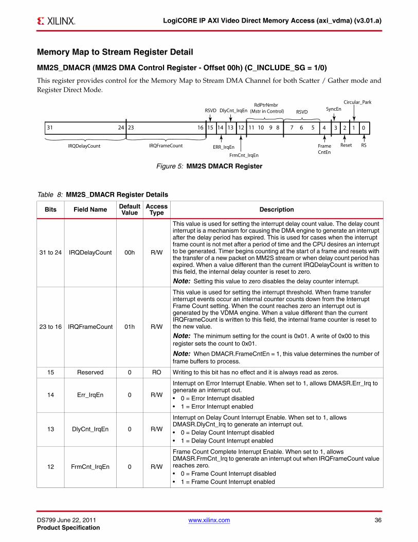
MM2S_DMACR (MM2S DMA Control Register - Offset 00h) (C_INCLUDE_SG = 1/0)
This register provides control for the Memory Map to Stream DMA Channel for both Scatter / Gather mode andRegister Direct Mode.X-Ref Target - Figure 5
Figure 5: MM2S DMACR Register
Table 8: MM2S_DMACR Register Details
Bits Field Name DefaultValue
AccessType Description
31 to 24 IRQDelayCount 00h R/W
This value is used for setting the interrupt delay count value. The delay count interrupt is a mechanism for causing the DMA engine to generate an interrupt after the delay period has expired. This is used for cases when the interrupt frame count is not met after a period of time and the CPU desires an interrupt to be generated. Timer begins counting at the start of a frame and resets with the transfer of a new packet on MM2S stream or when delay count period has expired. When a value different than the current IRQDelayCount is written to this field, the internal delay counter is reset to zero.
Note: Setting this value to zero disables the delay counter interrupt.
23 to 16 IRQFrameCount 01h R/W
This value is used for setting the interrupt threshold. When frame transfer interrupt events occur an internal counter counts down from the Interrupt Frame Count setting. When the count reaches zero an interrupt out is generated by the VDMA engine. When a value different than the current IRQFrameCount is written to this field, the internal frame counter is reset to the new value.
Note: The minimum setting for the count is 0x01. A write of 0x00 to this register sets the count to 0x01.
Note: When DMACR.FrameCntEn = 1, this value determines the number of frame buffers to process.
15 Reserved 0 RO Writing to this bit has no effect and it is always read as zeros.
14 Err_IrqEn 0 R/W
Interrupt on Error Interrupt Enable. When set to 1, allows DMASR.Err_Irq to generate an interrupt out.• 0 = Error Interrupt disabled• 1 = Error Interrupt enabled
13 DlyCnt_IrqEn 0 R/W
Interrupt on Delay Count Interrupt Enable. When set to 1, allows DMASR.DlyCnt_Irq to generate an interrupt out.• 0 = Delay Count Interrupt disabled• 1 = Delay Count Interrupt enabled
12 FrmCnt_IrqEn 0 R/W
Frame Count Complete Interrupt Enable. When set to 1, allows DMASR.FrmCnt_Irq to generate an interrupt out when IRQFrameCount value reaches zero.• 0 = Frame Count Interrupt disabled• 1 = Frame Count Interrupt enabled
RSVD DlyCnt_IrqEn RdPtrNmbr(Mstr in Control)
1516 14 13 12 11 10 931 24 23 8 7 6 5 4
RSVD
3 2 1
Circular_Park
0
IRQDelayCount IRQFrameCount ERR_IrqEn
FrmCnt_IrqEn
RSFrameCntEn
Reset
SyncEn
DS799 June 22, 2011 www.xilinx.com 37Product Specification
LogiCORE IP AXI Video Direct Memory Access (axi_vdma) (v3.01.a)
11 to 8 RdPntrNum zeros RW
Indicates the master in control when MM2S channel is configured for Gen-Lock slave mode (C_MM2S_GENLOCK_MODE = 1).0000b = Controlling master is Master 10001b = Controller master is Master 20010b = Controller master is Master 3etc.
Note: Maximum valid RdPntrNum is C_MM2S_GENLOCK_NUM_MASTER - 1. Setting to a value greater than C_MM2S_GENLOCK_NUM_MASTER - 1 has undefined results.
7 to 5 Reserved 0 RO Writing to these bits has no effect, and they are always read as zeros.
4 FrameCntEn 0 RW
Configures MM2S channel to only allow IRQFrameCount number of transfers to occur. After IRQFrameCount frames have been transferred the MM2S channel halts, DMACR.RS bit is cleared to 0 and DMASR.Halted asserts to 1 when the channel has completely halted.
3 SyncEn 0 RW
Enables Gen-Lock synchronization.• 0 = Gen-Lock synchronization disabled. Gen-Lock input ignored by MM2S• 1 = Gen-Lock synchronization enabled. MM2S synchronized to Gen-Lock
frame input.
Note: This value is only valid when channel configured as Gen-Lock Slave (C_MM2S_GENLOCK_MODE = 1). If configured for Gen-Lock Master mode (C_MM2S_GENLOCK_MODE = 0) then this bit is reserved and always reads as zero.
2 Reset 0 RW
Soft reset for resetting the AXI VDMA MM2S channel. Setting this bit to a 1 causes the AXI VDMA MM2S channel to be reset. Reset is accomplished gracefully. Pending commands/transfers are flushed or completed. AXI4-Stream reset output is asserted. Setting DMACR.Reset = 1 only resets the MM2S channel. After completion of a soft reset all MM2S registers and bits are in the Reset State• 0 = Reset NOT in progress - Normal operation• 1 = Reset in progress
1 Circular_Park 1 RO
Indicates frame buffer Circular mode or frame buffer Park mode.0 = Park Mode- Engine will park on frame buffer referenced by PARK_PTR_REG.RdFrmPntrRef.1 = Circular Mode - Engine continuously circles through MM2S_FRMSTORE frame buffers.
0 RS 0 R/W
Run / Stop controls running and stopping of the VDMA channel. For any DMA operations to commence the AXI VDMA engine must be running (DMACR.RS=1)• 0 = Stop - VDMA stops when current (if any) DMA operations are complete.
Queued descriptors for the associated channel are flushed from the SG Engine. The halted bit in the DMA Status Register asserts to 1 when the DMA engine is halted. This bit gets cleared by AXI VDMA hardware when an error occurs or when the IRQFrameCount is reached when Frame Count Enable is asserted (DMACR.FrameCntEn = 1). The CPU can also choose to clear this bit to stop DMA operations.
• 1 = Run - Start DMA operations. The halted bit in the DMA Status Register deasserts to 0 when the DMA engine begins operations.
Note: On Run/Stop clear, in progress stream transfers might terminate early.
RO = Read Only. Writing has no effect.R/W = Read / Write.
Table 8: MM2S_DMACR Register Details (Cont’d)
Bits Field Name DefaultValue
AccessType Description
DS799 June 22, 2011 www.xilinx.com 38Product Specification
LogiCORE IP AXI Video Direct Memory Access (axi_vdma) (v3.01.a)
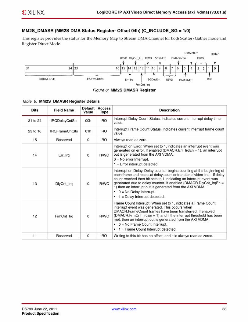
MM2S_DMASR (MM2S DMA Status Register- Offset 04h) (C_INCLUDE_SG = 1/0)
This register provides the status for the Memory Map to Stream DMA Channel for both Scatter/Gather mode andRegister Direct Mode.X-Ref Target - Figure 6
Figure 6: MM2S DMASR Register
Table 9: MM2S_DMASR Register Details
Bits Field Name Default Value
Access Type Description
31 to 24 IRQDelayCntSts 00h RO Interrupt Delay Count Status. Indicates current interrupt delay time value.
23 to 16 IRQFrameCntSts 01h RO Interrupt Frame Count Status. Indicates current interrupt frame count value.
15 Reserved 0 RO Always read as zero.
14 Err_Irq 0 R/WC
Interrupt on Error. When set to 1, indicates an interrupt event was generated on error. If enabled (DMACR.Err_IrqEn = 1), an interrupt out is generated from the AXI VDMA.0 = No error Interrupt.1 = Error interrupt detected.
13 DlyCnt_Irq 0 R/WC
Interrupt on Delay. Delay counter begins counting at the beginning of each frame and resets at delay count or transfer of video line. If delay count reached then bit sets to 1 indicating an interrupt event was generated due to delay counter. If enabled (DMACR.DlyCnt_IrqEn = 1) then an interrupt out is generated from the AXI VDMA.• 0 = No Delay Interrupt.• 1 = Delay Interrupt detected.
12 FrmCnt_Irq 0 R/WC
Frame Count Interrupt. When set to 1, indicates a Frame Count interrupt event was generated. This occurs when DMACR.FrameCount frames have been transferred. If enabled (DMACR.FrmCnt_IrqEn = 1) and if the interrupt threshold has been met, then an interrupt out is generated from the AXI VDMA.• 0 = No Frame Count Interrupt.• 1 = Frame Count Interrupt detected.
11 Reserved 0 RO Writing to this bit has no effect, and it is always read as zeros.
RSVD DlyCnt_Irq RSVD SGSIvErr DMADecErr
1516 14 13 12 11 10 9
DMAIntErr
31 24 23 8 7 6 5 4
RSVD
3 2 1
Halted
0
IRQDlyCntSts IRQFmCntSts Err_Irq
FrmCnt_Irq
SGDecErr IdleRSVD DMASIvErr
DS799 June 22, 2011 www.xilinx.com 39Product Specification
LogiCORE IP AXI Video Direct Memory Access (axi_vdma) (v3.01.a)
10 SGDecErr 0 RO
Scatter Gather Decode Error. In Scatter / Gather Mode (C_INCLUDE_SG =1) this bit indicates a Decode Error was detected by the Scatter Gather Engine. This error occurs if the address request is to an invalid address (that is, CURDESC and/or NXTDESC points to an invalid address). This error condition causes both AXI VDMA channels (MM2S and S2MM) to gracefully halt. The DMACR.RS bit is set to 0, and when the engine has completely shut down, the DMASR.Halted bit is set to 1 for both channels.For Register Direct Mode (C_INCLUDE_SG = 0) this bit is reserved and always read as 0b.• 0 = No SG Decode Errors.• 1 = SG Decode Error detected. DMA Engine halts.
Note: In Scatter / Gather Mode (C_INCLUDE_SG = 1) the CURDESC register is updated with the errored descriptor pointer when this error is detected. If multiple errors are detected, the errors are logged in the DMASR, but only one address is updated to the CURDESC. A reset (soft or hard) must be issued to clear the error condition.
Note: On Error, in progress stream transfers might terminate early.
9 SGSlvErr 0 RO
Scatter Gather Slave Error. In Scatter / Gather Mode (C_INCLUDE_SG =1) this bit indicates a Slave Error was detected by the Scatter Gather Engine. This error occurs if the slave read from on the Memory Map interface issues a Slave error. This error condition causes both AXI VDMA channels (MM2S and S2MM) to gracefully halt. The DMACR.RS bit is set to 0, and when the engine has completely shut down, the DMASR.Halted bit is set to 1 for both channels.For Register Direct Mode (C_INCLUDE_SG = 0) this bit is reserved and always read as 0b.• 0 = No SG Slave Errors.• 1 = SG Slave Error detected. DMA Engine halts.
Note: In Scatter / Gather Mode (C_INCLUDE_SG = 1) the CURDESC register is updated with the errored descriptor pointer when this error is detected. If multiple errors are detected, the errors are logged in the DMASR, but only one address is updated to the CURDESC. A reset (soft or hard) must be issued to clear the error condition.
Note: On Error, in progress stream transfers might terminate early.
8 to 7 Reserved zeros RO Writing to these bits has no effect, and they are always read as zeros.
Table 9: MM2S_DMASR Register Details (Cont’d)
Bits Field Name Default Value
Access Type Description
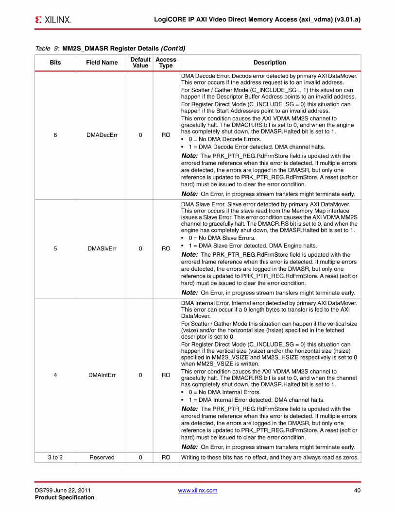
DS799 June 22, 2011 www.xilinx.com 40Product Specification
LogiCORE IP AXI Video Direct Memory Access (axi_vdma) (v3.01.a)
6 DMADecErr 0 RO
DMA Decode Error. Decode error detected by primary AXI DataMover. This error occurs if the address request is to an invalid address.For Scatter / Gather Mode (C_INCLUDE_SG = 1) this situation can happen if the Descriptor Buffer Address points to an invalid address.For Register Direct Mode (C_INCLUDE_SG = 0) this situation can happen if the Start Address/es point to an invalid address.This error condition causes the AXI VDMA MM2S channel to gracefully halt. The DMACR.RS bit is set to 0, and when the engine has completely shut down, the DMASR.Halted bit is set to 1.• 0 = No DMA Decode Errors.• 1 = DMA Decode Error detected. DMA channel halts.
Note: The PRK_PTR_REG.RdFrmStore field is updated with the errored frame reference when this error is detected. If multiple errors are detected, the errors are logged in the DMASR, but only one reference is updated to PRK_PTR_REG.RdFrmStore. A reset (soft or hard) must be issued to clear the error condition.
Note: On Error, in progress stream transfers might terminate early.
5 DMASlvErr 0 RO
DMA Slave Error. Slave error detected by primary AXI DataMover. This error occurs if the slave read from the Memory Map interface issues a Slave Error. This error condition causes the AXI VDMA MM2S channel to gracefully halt. The DMACR.RS bit is set to 0, and when the engine has completely shut down, the DMASR.Halted bit is set to 1.• 0 = No DMA Slave Errors.• 1 = DMA Slave Error detected. DMA Engine halts.
Note: The PRK_PTR_REG.RdFrmStore field is updated with the errored frame reference when this error is detected. If multiple errors are detected, the errors are logged in the DMASR, but only one reference is updated to PRK_PTR_REG.RdFrmStore. A reset (soft or hard) must be issued to clear the error condition.
Note: On Error, in progress stream transfers might terminate early.
4 DMAIntErr 0 RO
DMA Internal Error. Internal error detected by primary AXI DataMover. This error can occur if a 0 length bytes to transfer is fed to the AXI DataMover. For Scatter / Gather Mode this situation can happen if the vertical size (vsize) and/or the horizontal size (hsize) specified in the fetched descriptor is set to 0.For Register Direct Mode (C_INCLUDE_SG = 0) this situation can happen if the vertical size (vsize) and/or the horizontal size (hsize) specified in MM2S_VSIZE and MM2S_HSIZE respectively is set to 0 when MM2S_VSIZE is written.This error condition causes the AXI VDMA MM2S channel to gracefully halt. The DMACR.RS bit is set to 0, and when the channel has completely shut down, the DMASR.Halted bit is set to 1.• 0 = No DMA Internal Errors.• 1 = DMA Internal Error detected. DMA channel halts.
Note: The PRK_PTR_REG.RdFrmStore field is updated with the errored frame reference when this error is detected. If multiple errors are detected, the errors are logged in the DMASR, but only one reference is updated to PRK_PTR_REG.RdFrmStore. A reset (soft or hard) must be issued to clear the error condition.
Note: On Error, in progress stream transfers might terminate early.
3 to 2 Reserved 0 RO Writing to these bits has no effect, and they are always read as zeros.
Table 9: MM2S_DMASR Register Details (Cont’d)
Bits Field Name Default Value
Access Type Description
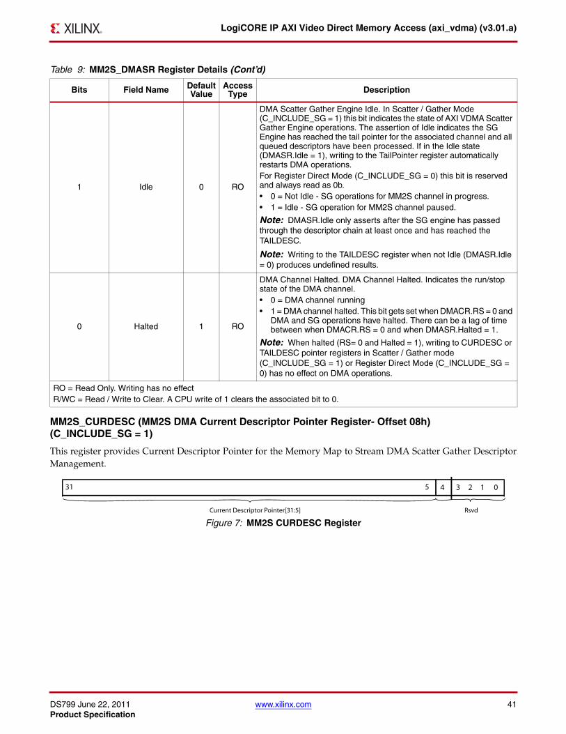
DS799 June 22, 2011 www.xilinx.com 41Product Specification
LogiCORE IP AXI Video Direct Memory Access (axi_vdma) (v3.01.a)
MM2S_CURDESC (MM2S DMA Current Descriptor Pointer Register- Offset 08h) (C_INCLUDE_SG = 1)
This register provides Current Descriptor Pointer for the Memory Map to Stream DMA Scatter Gather DescriptorManagement.
1 Idle 0 RO
DMA Scatter Gather Engine Idle. In Scatter / Gather Mode (C_INCLUDE_SG = 1) this bit indicates the state of AXI VDMA Scatter Gather Engine operations. The assertion of Idle indicates the SG Engine has reached the tail pointer for the associated channel and all queued descriptors have been processed. If in the Idle state (DMASR.Idle = 1), writing to the TailPointer register automatically restarts DMA operations.For Register Direct Mode (C_INCLUDE_SG = 0) this bit is reserved and always read as 0b.• 0 = Not Idle - SG operations for MM2S channel in progress.• 1 = Idle - SG operation for MM2S channel paused.
Note: DMASR.Idle only asserts after the SG engine has passed through the descriptor chain at least once and has reached the TAILDESC.
Note: Writing to the TAILDESC register when not Idle (DMASR.Idle = 0) produces undefined results.
0 Halted 1 RO
DMA Channel Halted. DMA Channel Halted. Indicates the run/stop state of the DMA channel.• 0 = DMA channel running• 1 = DMA channel halted. This bit gets set when DMACR.RS = 0 and
DMA and SG operations have halted. There can be a lag of time between when DMACR.RS = 0 and when DMASR.Halted = 1.
Note: When halted (RS= 0 and Halted = 1), writing to CURDESC or TAILDESC pointer registers in Scatter / Gather mode (C_INCLUDE_SG = 1) or Register Direct Mode (C_INCLUDE_SG = 0) has no effect on DMA operations.
RO = Read Only. Writing has no effectR/WC = Read / Write to Clear. A CPU write of 1 clears the associated bit to 0.
X-Ref Target - Figure 7
Figure 7: MM2S CURDESC Register
Table 9: MM2S_DMASR Register Details (Cont’d)
Bits Field Name Default Value
Access Type Description
31 5 4 3 2 1 0
Current Descriptor Pointer[31:5] Rsvd
DS799 June 22, 2011 www.xilinx.com 42Product Specification
LogiCORE IP AXI Video Direct Memory Access (axi_vdma) (v3.01.a)
Table 10: MM2S_CURDESC Register Details
Bits Field Name Default Value
Access Type Description
31 to 5 Current Descriptor Pointer zeros
R/W(RO)
In Scatter / Gather Mode (C_INCLUDE_SG = 1) indicates the pointer of the current descriptor being worked on. This register must contain a pointer to a valid descriptor prior to writing the TAILDESC register. Otherwise, undefined results occur. When DMACR.RS is 1, CURDESC becomes Read Only (RO) and is used to fetch the first descriptor. When the DMA Engine is running (DMACR.RS=1), CURDESC registers are updated by AXI VDMA to indicate the current descriptor being worked on. On Scatter Gather error detection, CURDESC is updated to reflect the descriptor associated with the detected error.The register can only be written to by the CPU when the DMA Engine is Halted (DMACR.RS=0 and DMASR.Halted =1). At all other times, this register is Read Only (RO). Descriptors must be 8 word aligned, that is, 0x00, 0x20, 0x40, etc. Any other alignment has undefined results.In Register Direct Mode (C_INCLUDE_SG = 0) this field is reserved and always read as zeros.
4 to 0 Reserved 0 RO Writing to these bits has no effect, and they are always read as zeros.
RO = Read Only. Writing has no effect.R/W = Read / Write.
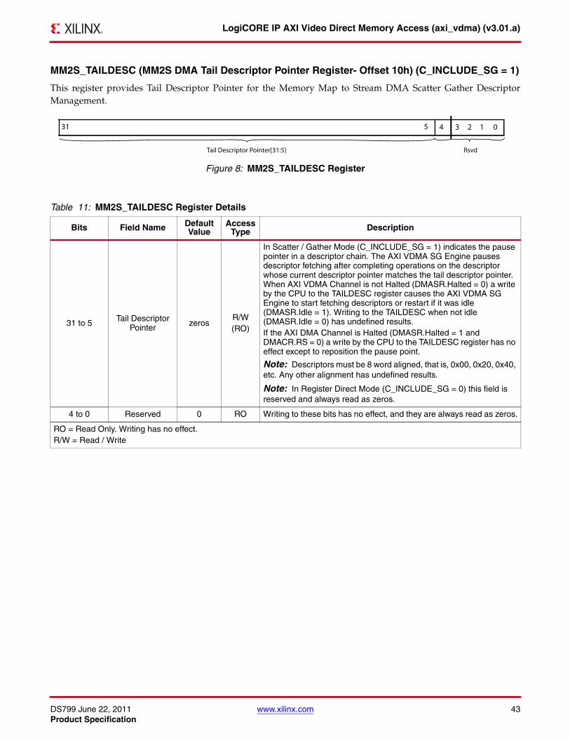
DS799 June 22, 2011 www.xilinx.com 43Product Specification
LogiCORE IP AXI Video Direct Memory Access (axi_vdma) (v3.01.a)
MM2S_TAILDESC (MM2S DMA Tail Descriptor Pointer Register- Offset 10h) (C_INCLUDE_SG = 1)
This register provides Tail Descriptor Pointer for the Memory Map to Stream DMA Scatter Gather DescriptorManagement.X-Ref Target - Figure 8
Figure 8: MM2S_TAILDESC Register
Table 11: MM2S_TAILDESC Register Details
Bits Field Name Default Value
Access Type Description
31 to 5 Tail Descriptor Pointer zeros
R/W(RO)
In Scatter / Gather Mode (C_INCLUDE_SG = 1) indicates the pause pointer in a descriptor chain. The AXI VDMA SG Engine pauses descriptor fetching after completing operations on the descriptor whose current descriptor pointer matches the tail descriptor pointer. When AXI VDMA Channel is not Halted (DMASR.Halted = 0) a write by the CPU to the TAILDESC register causes the AXI VDMA SG Engine to start fetching descriptors or restart if it was idle (DMASR.Idle = 1). Writing to the TAILDESC when not idle (DMASR.Idle = 0) has undefined results.If the AXI DMA Channel is Halted (DMASR.Halted = 1 and DMACR.RS = 0) a write by the CPU to the TAILDESC register has no effect except to reposition the pause point.
Note: Descriptors must be 8 word aligned, that is, 0x00, 0x20, 0x40, etc. Any other alignment has undefined results.
Note: In Register Direct Mode (C_INCLUDE_SG = 0) this field is reserved and always read as zeros.
4 to 0 Reserved 0 RO Writing to these bits has no effect, and they are always read as zeros.
RO = Read Only. Writing has no effect.R/W = Read / Write
31 5 4 3 2 1 0
Tail Descriptor Pointer[31:5] Rsvd
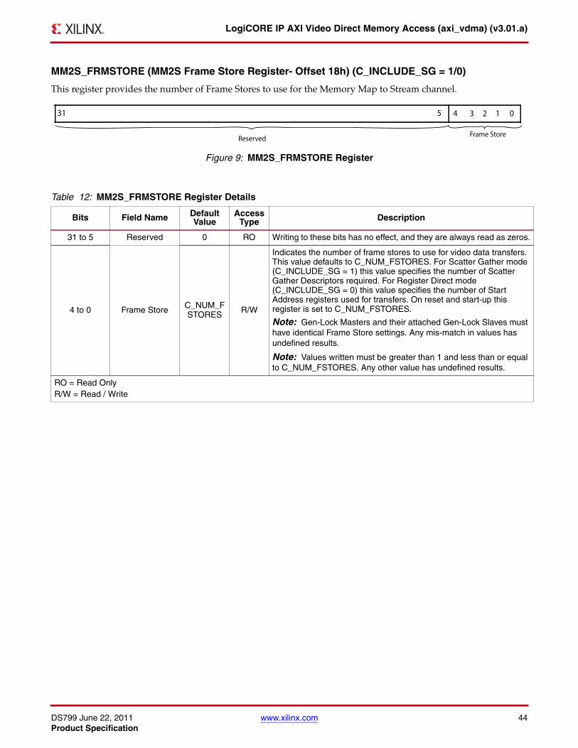
DS799 June 22, 2011 www.xilinx.com 44Product Specification
LogiCORE IP AXI Video Direct Memory Access (axi_vdma) (v3.01.a)
MM2S_FRMSTORE (MM2S Frame Store Register- Offset 18h) (C_INCLUDE_SG = 1/0)
This register provides the number of Frame Stores to use for the Memory Map to Stream channel.X-Ref Target - Figure 9
Figure 9: MM2S_FRMSTORE Register
Table 12: MM2S_FRMSTORE Register Details
Bits Field Name Default Value
Access Type Description
31 to 5 Reserved 0 RO Writing to these bits has no effect, and they are always read as zeros.
4 to 0 Frame Store C_NUM_FSTORES R/W
Indicates the number of frame stores to use for video data transfers. This value defaults to C_NUM_FSTORES. For Scatter Gather mode (C_INCLUDE_SG = 1) this value specifies the number of Scatter Gather Descriptors required. For Register Direct mode (C_INCLUDE_SG = 0) this value specifies the number of Start Address registers used for transfers. On reset and start-up this register is set to C_NUM_FSTORES.
Note: Gen-Lock Masters and their attached Gen-Lock Slaves must have identical Frame Store settings. Any mis-match in values has undefined results.
Note: Values written must be greater than 1 and less than or equal to C_NUM_FSTORES. Any other value has undefined results.
RO = Read OnlyR/W = Read / Write
31 5 4 3 2 1 0
ReservedFrame Store
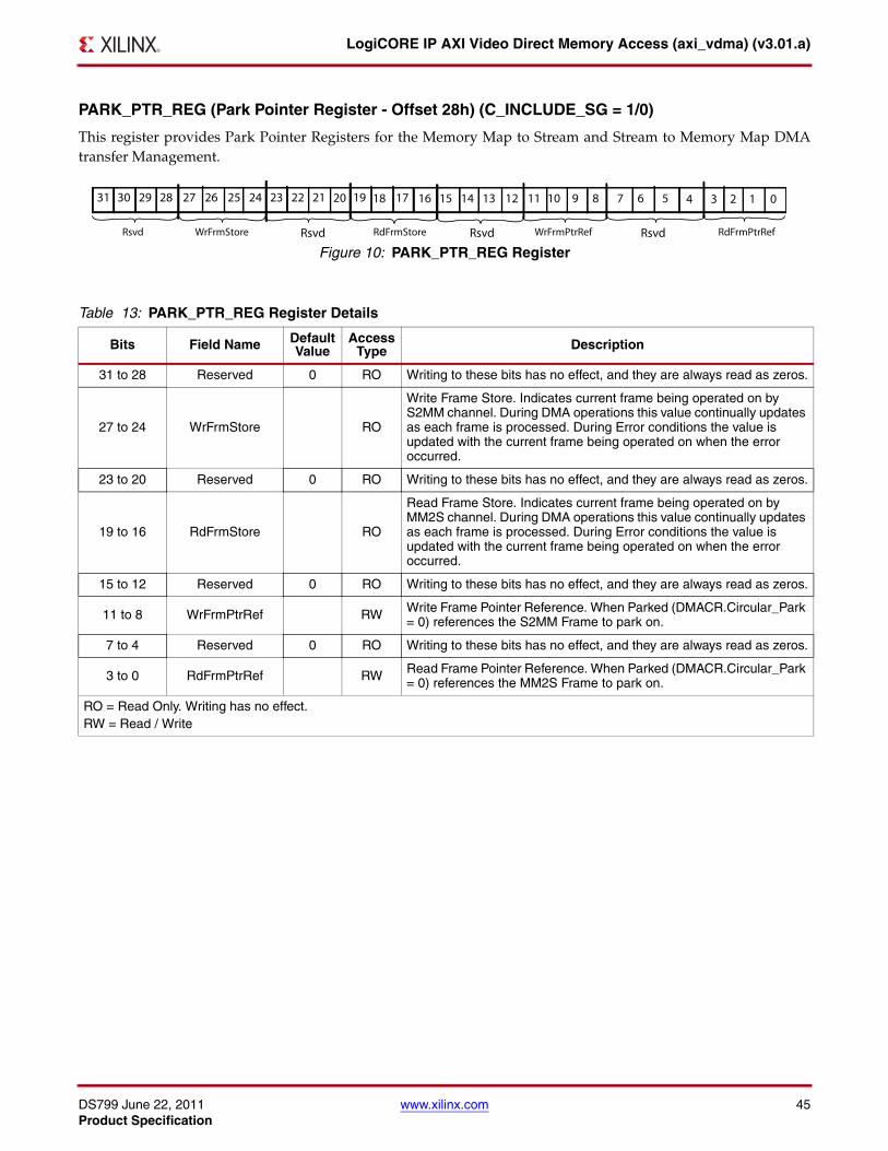
DS799 June 22, 2011 www.xilinx.com 45Product Specification
LogiCORE IP AXI Video Direct Memory Access (axi_vdma) (v3.01.a)
PARK_PTR_REG (Park Pointer Register - Offset 28h) (C_INCLUDE_SG = 1/0)
This register provides Park Pointer Registers for the Memory Map to Stream and Stream to Memory Map DMAtransfer Management.X-Ref Target - Figure 10
Figure 10: PARK_PTR_REG Register
Table 13: PARK_PTR_REG Register Details
Bits Field Name Default Value
Access Type Description
31 to 28 Reserved 0 RO Writing to these bits has no effect, and they are always read as zeros.
27 to 24 WrFrmStore RO
Write Frame Store. Indicates current frame being operated on by S2MM channel. During DMA operations this value continually updates as each frame is processed. During Error conditions the value is updated with the current frame being operated on when the error occurred.
23 to 20 Reserved 0 RO Writing to these bits has no effect, and they are always read as zeros.
19 to 16 RdFrmStore RO
Read Frame Store. Indicates current frame being operated on by MM2S channel. During DMA operations this value continually updates as each frame is processed. During Error conditions the value is updated with the current frame being operated on when the error occurred.
15 to 12 Reserved 0 RO Writing to these bits has no effect, and they are always read as zeros.
11 to 8 WrFrmPtrRef RW Write Frame Pointer Reference. When Parked (DMACR.Circular_Park = 0) references the S2MM Frame to park on.
7 to 4 Reserved 0 RO Writing to these bits has no effect, and they are always read as zeros.
3 to 0 RdFrmPtrRef RW Read Frame Pointer Reference. When Parked (DMACR.Circular_Park = 0) references the MM2S Frame to park on.
RO = Read Only. Writing has no effect.RW = Read / Write
1516 14 13 12 11 10 931 24 23 8 7 6 5 4 3 2 1 0
Rsvd WrFrmStore
30 29 28 27 2526 22 21 20 19 18 17
Rsvd RdFrmStore Rsvd RsvdWrFrmPtrRef RdFrmPtrRef
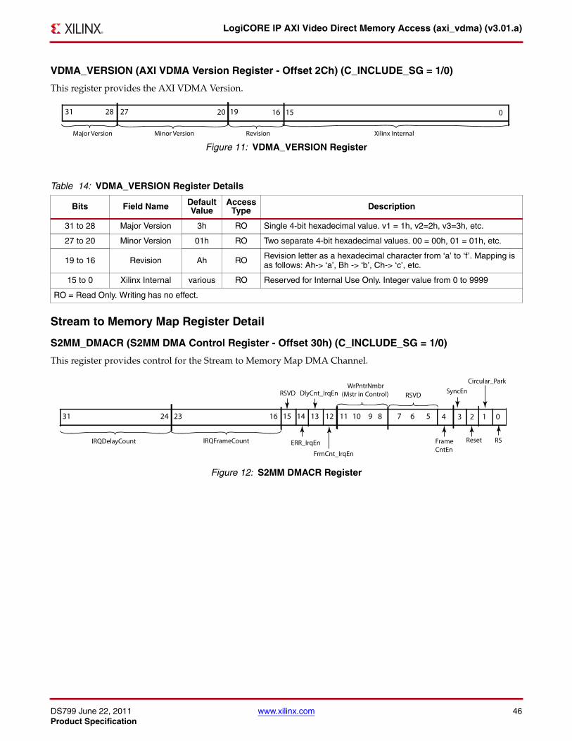
DS799 June 22, 2011 www.xilinx.com 46Product Specification
LogiCORE IP AXI Video Direct Memory Access (axi_vdma) (v3.01.a)
VDMA_VERSION (AXI VDMA Version Register - Offset 2Ch) (C_INCLUDE_SG = 1/0)
This register provides the AXI VDMA Version.
Stream to Memory Map Register Detail
S2MM_DMACR (S2MM DMA Control Register - Offset 30h) (C_INCLUDE_SG = 1/0)
This register provides control for the Stream to Memory Map DMA Channel.
X-Ref Target - Figure 11
Figure 11: VDMA_VERSION Register
Table 14: VDMA_VERSION Register Details
Bits Field Name Default Value
Access Type Description
31 to 28 Major Version 3h RO Single 4-bit hexadecimal value. v1 = 1h, v2=2h, v3=3h, etc.
27 to 20 Minor Version 01h RO Two separate 4-bit hexadecimal values. 00 = 00h, 01 = 01h, etc.
19 to 16 Revision Ah RO Revision letter as a hexadecimal character from ‘a’ to ‘f’. Mapping is as follows: Ah-> ‘a’, Bh -> ‘b’, Ch-> ‘c’, etc.
15 to 0 Xilinx Internal various RO Reserved for Internal Use Only. Integer value from 0 to 9999
RO = Read Only. Writing has no effect.
X-Ref Target - Figure 12
Figure 12: S2MM DMACR Register
151631 028 27 20 19
Minor VersionMajor Version Revision Xilinx Internal
RSVD DlyCnt_IrqEn WrPntrNmbr(Mstr in Control)
1516 14 13 12 11 10 931 24 23 8 7 6 5 4
RSVD
3 2 1 0
IRQDelayCount IRQFrameCount ERR_IrqEn
FrmCnt_IrqEn
RSFrameCntEn
Reset
SyncEn
Circular_Park
DS799 June 22, 2011 www.xilinx.com 47Product Specification
LogiCORE IP AXI Video Direct Memory Access (axi_vdma) (v3.01.a)
Table 15: S2MM_DMACR Register Details
Bits Field Name DefaultValue
AccessType Description
31 to 24 IRQDelayCount 00h R/W
This value is used for setting the interrupt delay count value. The delay count interrupt is a mechanism for causing the DMA engine to generate an interrupt after the delay period has expired. This is used for cases when the interrupt frame count is not met after a period of time and the CPU desires an interrupt to be generated. Timer begins counting at the start of a frame and resets with the transfer of a new packet on S2MM stream or when delay count period has expired. When a value different than the current IRQDelayCount is written to this field, the internal delay counter is reset to zero.
Note: Setting this value to zero disables the delay counter interrupt.
23 to 16 IRQFrameCount 01h R/W
This value is used for setting the interrupt threshold. When frame transfer interrupt events occur an internal counter counts down from the Interrupt Frame Count setting. When the count reaches zero an interrupt out is generated by the VDMA engine. When a value different than the current IRQFrameCount is written to this field, the internal frame counter is reset to the new value.
Note: The minimum setting for the count is 0x01. A write of 0x00 to this register sets the count to 0x01.
Note: When DMACR.FrameCntEn = 1, this value determines the number of frame buffers to process.
15 Reserved 0 RO Writing to this bit has no effect and it is always read as zeros.
14 Err_IrqEn 0 R/W
Interrupt on Error Interrupt Enable. When set to 1, allows DMASR.Err_Irq to generate an interrupt out.• 0 = Error Interrupt disabled• 1 = Error Interrupt enabled
13 DlyCnt_IrqEn 0 R/W
Interrupt on Delay Count Interrupt Enable. When set to 1, allows DMASR.DlyCnt_Irq to generate an interrupt out.• 0 = Delay Count Interrupt disabled• 1 = Delay Count Interrupt enabled
12 FrmCnt_IrqEn 0 R/W
Frame Count Complete Interrupt Enable. When set to 1, allows DMASR.FrmCnt_Irq to generate an interrupt out when IRQFrameCount value reaches zero.• 0 = Frame Count Interrupt disabled• 1 = Frame Count Interrupt enabled
11 to 8 WrPntrNum zeros RW
Indicates the master in control when S2MM channel is configured for Gen-Lock slave mode (C_S2MM_GENLOCK_MODE = 1).0000b = Controlling master is Master 1.0001b = Controller master is Master 2.0010b = Controller master is Master 3.etc.
Note: Maximum valid RdPntrNum is C_S2MM_GENLOCK_NUM_MASTER - 1. Setting to a value greater than C_S2MM_GENLOCK_NUM_MASTER - 1 has undefined results.
7 to 5 Reserved 0 RO Writing to these bits has no effect, and they are always read as zeros.
4 FrameCntEn 0 RW
Configures MM2S channel to only allow IRQFrameCount number of transfers to occur. After IRQFrameCount frames have been transferred the S2MM channel halts, DMACR.RS bit is cleared to 0 and DMASR.Halted asserts to 1 when the channel has completely halted.
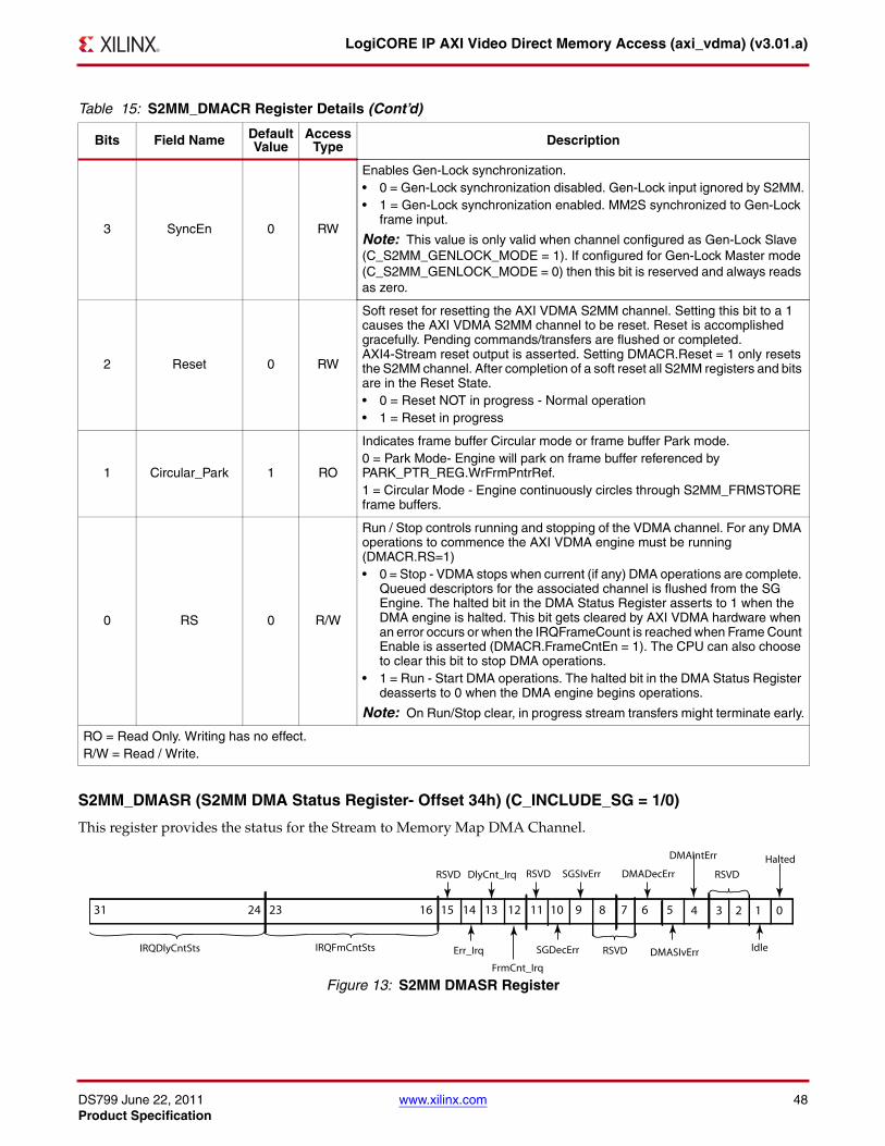
DS799 June 22, 2011 www.xilinx.com 48Product Specification
LogiCORE IP AXI Video Direct Memory Access (axi_vdma) (v3.01.a)
S2MM_DMASR (S2MM DMA Status Register- Offset 34h) (C_INCLUDE_SG = 1/0)
This register provides the status for the Stream to Memory Map DMA Channel.
3 SyncEn 0 RW
Enables Gen-Lock synchronization.• 0 = Gen-Lock synchronization disabled. Gen-Lock input ignored by S2MM.• 1 = Gen-Lock synchronization enabled. MM2S synchronized to Gen-Lock
frame input.
Note: This value is only valid when channel configured as Gen-Lock Slave (C_S2MM_GENLOCK_MODE = 1). If configured for Gen-Lock Master mode (C_S2MM_GENLOCK_MODE = 0) then this bit is reserved and always reads as zero.
2 Reset 0 RW
Soft reset for resetting the AXI VDMA S2MM channel. Setting this bit to a 1 causes the AXI VDMA S2MM channel to be reset. Reset is accomplished gracefully. Pending commands/transfers are flushed or completed. AXI4-Stream reset output is asserted. Setting DMACR.Reset = 1 only resets the S2MM channel. After completion of a soft reset all S2MM registers and bits are in the Reset State.• 0 = Reset NOT in progress - Normal operation• 1 = Reset in progress
1 Circular_Park 1 RO
Indicates frame buffer Circular mode or frame buffer Park mode.0 = Park Mode- Engine will park on frame buffer referenced by PARK_PTR_REG.WrFrmPntrRef.1 = Circular Mode - Engine continuously circles through S2MM_FRMSTORE frame buffers.
0 RS 0 R/W
Run / Stop controls running and stopping of the VDMA channel. For any DMA operations to commence the AXI VDMA engine must be running (DMACR.RS=1)• 0 = Stop - VDMA stops when current (if any) DMA operations are complete.
Queued descriptors for the associated channel is flushed from the SG Engine. The halted bit in the DMA Status Register asserts to 1 when the DMA engine is halted. This bit gets cleared by AXI VDMA hardware when an error occurs or when the IRQFrameCount is reached when Frame Count Enable is asserted (DMACR.FrameCntEn = 1). The CPU can also choose to clear this bit to stop DMA operations.
• 1 = Run - Start DMA operations. The halted bit in the DMA Status Register deasserts to 0 when the DMA engine begins operations.
Note: On Run/Stop clear, in progress stream transfers might terminate early.
RO = Read Only. Writing has no effect.R/W = Read / Write.
X-Ref Target - Figure 13
Figure 13: S2MM DMASR Register
Table 15: S2MM_DMACR Register Details (Cont’d)
Bits Field Name DefaultValue
AccessType Description
RSVD DlyCnt_Irq RSVD SGSIvErr DMADecErr
1516 14 13 12 11 10 9
DMAIntErr
31 24 23 8 7 6 5 4
RSVD
3 2 1
Halted
0
IRQDlyCntSts IRQFmCntSts Err_Irq
FrmCnt_Irq
SGDecErr IdleRSVD DMASIvErr
DS799 June 22, 2011 www.xilinx.com 49Product Specification
LogiCORE IP AXI Video Direct Memory Access (axi_vdma) (v3.01.a)
Table 16: S2MM_DMASR Register Details
Bits Field Name Default Value
Access Type Description
31 to 24 IRQDelayCntSts 00h RO Interrupt Delay Count Status. Indicates current interrupt delay time value.
23 to 16 IRQFrameCntSts 01h RO Interrupt Frame Count Status. Indicates current interrupt frame count value.
15 Reserved 0 RO Always read as zero.
14 Err_Irq 0 R/WC
Interrupt on Error. When set to 1, indicates an interrupt event was generated on error. If enabled (DMACR.Err_IrqEn = 1), an interrupt out is generated from the AXI VDMA.0 = No error Interrupt.1 = Error interrupt detected.
13 DlyCnt_Irq 0 R/WC
Interrupt on Delay. Delay counter begins counting at the beginning of each frame and resets at delay count or transfer of video line. If delay count reached then bit sets to 1 indicating an interrupt event was generated due to delay counter. If enabled (DMACR.DlyCnt_IrqEn = 1) then an interrupt out is generated from the AXI VDMA.• 0 = No Delay Interrupt.• 1 = Delay Interrupt detected.
12 FrmCnt_Irq 0 R/WC
Frame Count Interrupt. When set to 1, indicates a Frame Count interrupt event was generated. This occurs when DMACR.FrameCount frames have been transferred. If enabled (DMACR.FrmCnt_IrqEn = 1) and if the interrupt threshold has been met, then an interrupt out is generated from the AXI VDMA.• 0 = No Frame Count Interrupt.• 1 = Frame Count Interrupt detected.
11 Reserved 0 RO Writing to this bit has no effect, and it is always read as zeros.
10 SGDecErr 0 RO
Scatter Gather Decode Error. In Scatter / Gather Mode (C_INCLUDE_SG =1) this bit indicates a Decode Error was detected by the Scatter Gather Engine - This error occurs if the address request is to an invalid address (that is, CURDESC and/or NXTDESC points to an invalid address). This error condition causes both AXI VDMA channels (MM2S and S2MM) to gracefully halt. The DMACR.RS bit is set to 0, and when the engine has completely shut down, the DMASR.Halted bit is set to 1 for both channels.For Register Direct Mode (C_INCLUDE_SG = 0) this bit is reserved and always read as 0b.• 0 = No SG Decode Errors.• 1 = SG Decode Error detected. DMA Engine halts.
Note: In Scatter / Gather Mode (C_INCLUDE_SG = 1) the CURDESC register is updated with the errored descriptor pointer when this error is detected. If multiple errors are detected, the errors are logged in the DMASR, but only one address is updated to the CURDESC. A reset (soft or hard) must be issued to clear the error condition.
Note: On Error, in progress stream transfers might terminate early.
DS799 June 22, 2011 www.xilinx.com 50Product Specification
LogiCORE IP AXI Video Direct Memory Access (axi_vdma) (v3.01.a)
9 SGSlvErr 0 RO
Scatter Gather Slave Error. In Scatter / Gather Mode (C_INCLUDE_SG =1) this bit indicates a Slave Error was detected by the Scatter Gather Engine. This error occurs if the slave read from on the Memory Map interface issues a Slave error. This error condition causes both AXI VDMA channels (MM2S and S2MM) to gracefully halt. The DMACR.RS bit is set to 0, and when the engine has completely shut down, the DMASR.Halted bit is set to 1 for both channels.For Register Direct Mode (C_INCLUDE_SG = 0) this bit is reserved and always read as 0b.• 0 = No SG Slave Errors.• 1 = SG Slave Error detected. DMA Engine halts.
Note: In Scatter / Gather Mode (C_INCLUDE_SG = 1) the CURDESC register is updated with the errored descriptor pointer when this error is detected. If multiple errors are detected, the errors are logged in the DMASR, but only one address is updated to the CURDESC. A reset (soft or hard) must be issued to clear the error condition.
Note: On Error, in progress stream transfers might terminate early.
8 to 7 Reserved zeros RO Writing to these bits has no effect, and they are always read as zeros.
6 DMADecErr 0 RO
DMA Decode Error. Decode error detected by primary AXI DataMover. This error occurs if the address request is to an invalid address.For Scatter / Gather Mode (C_INCLUDE_SG = 1) this situation can happen if the Descriptor Buffer Address points to an invalid address.For Register Direct Mode (C_INCLUDE_SG = 0) this situation can happen if the Start Address/es point to an invalid address.This error condition causes the AXI VDMA S2MM channel to gracefully halt. The DMACR.RS bit is set to 0, and when the engine has completely shut down, the DMASR.Halted bit is set to 1.• 0 = No DMA Decode Errors.• 1 = DMA Decode Error detected. DMA channel halts.
Note: The PRK_PTR_REG.WrFrmStore field is updated with the errored frame reference when this error is detected. If multiple errors are detected, the errors are logged in the DMASR, but only one reference is updated to PRK_PTR_REG.WrFrmStore. A reset (soft or hard) must be issued to clear the error condition.
5 DMASlvErr 0 RO
DMA Slave Error. Slave error detected by primary AXI DataMover. This error occurs if the slave read from the Memory Map interface issues a Slave Error. This error condition causes the AXI VDMA S2MM channel to gracefully halt. The DMACR.RS bit is set to 0, and when the engine has completely shut down, the DMASR.Halted bit is set to 1.• 0 = No DMA Slave Errors.• 1 = DMA Slave Error detected. DMA Engine halts.
Note: The PRK_PTR_REG.WrFrmStore field is updated with the errored frame reference when this error is detected. If multiple errors are detected, the errors are logged in the DMASR, but only one reference is updated to PRK_PTR_REG.WrFrmStore. A reset (soft or hard) must be issued to clear the error condition.
Note: On Error, in progress stream transfers might terminate early.
Table 16: S2MM_DMASR Register Details (Cont’d)
Bits Field Name Default Value
Access Type Description
DS799 June 22, 2011 www.xilinx.com 51Product Specification
LogiCORE IP AXI Video Direct Memory Access (axi_vdma) (v3.01.a)
4 DMAIntErr 0 RO
DMA Internal Error. Internal error detected by primary AXI DataMover. This error can occur if a 0 length bytes to transfer is fed to the AXI DataMover. For Scatter / Gather Mode this situation can happen if the vertical size (vsize) and/or the horizontal size (hsize) specified in the fetched descriptor is set to 0.For Register Direct Mode (C_INCLUDE_SG = 0) this situation can happen if the vertical size (vsize) and/or the horizontal size (hsize) specified in S2MM_VSIZE and S2MM_HSIZE respectively is set to 0 when S2MM_VSIZE is written.This error can also occur if a packet greater or less than hsize bytes is received. This error condition causes the AXI VDMA S2MM channel to gracefully halt. The DMACR.RS bit is set to 0, and when the channel has completely shut down, the DMASR.Halted bit is set to 1.• 0 = No DMA Internal Errors.• 1 = DMA Internal Error detected. DMA channel halts.
Note: The PRK_PTR_REG.WrFrmStore field is updated with the errored frame reference when this error is detected. If multiple errors are detected, the errors are logged in the DMASR, but only one reference is updated to PRK_PTR_REG.WrFrmStore. A reset (soft or hard) must be issued to clear the error condition.
Note: On Error, in progress stream transfers might terminate early.
3 to 2 Reserved 0 RO Writing to these bits has no effect and they are always read as zeros.
1 Idle 0 RO
DMA Scatter Gather Engine Idle. In Scatter / Gather Mode (C_INCLUDE_SG = 1) this bit indicates the state of AXI VDMA Scatter Gather Engine operations. The assertion of Idle indicates the SG Engine has reached the tail pointer for the associated channel and all queued descriptors have been processed. If in the Idle state (DMASR.Idle = 1), writing to the TailPointer register automatically restarts DMA operations.For Register Direct Mode (C_INCLUDE_SG = 0) this bit is reserved and always read as 0b.• 0 = Not Idle - SG operations for S2MM channel in progress.• 1 = Idle - SG operation for S2MM channel paused.
Note: DMASR.Idle only asserts after the SG engine has passed through the descriptor chain at least once and has reached the TAILDESC.
Note: Writing to the TAILDESC register when not Idle (DMASR.Idle = 0) produces undefined results.
0 Halted 1 RO
DMA Channel Halted. DMA Channel Halted. Indicates the run/stop state of the DMA channel.• 0 = DMA channel running• 1 = DMA channel halted. This bit gets set when DMACR.RS = 0 and
DMA and SG operations have halted. There can be a lag of time between when DMACR.RS = 0 and when DMASR.Halted = 1.
Note: When halted (RS= 0 and Halted = 1), writing to CURDESC or TAILDESC pointer registers has no effect on DMA operations.
RO = Read Only. Writing has no effectR/WC = Read / Write to Clear. A CPU write of 1 clears the associated bit to 0.
Table 16: S2MM_DMASR Register Details (Cont’d)
Bits Field Name Default Value
Access Type Description
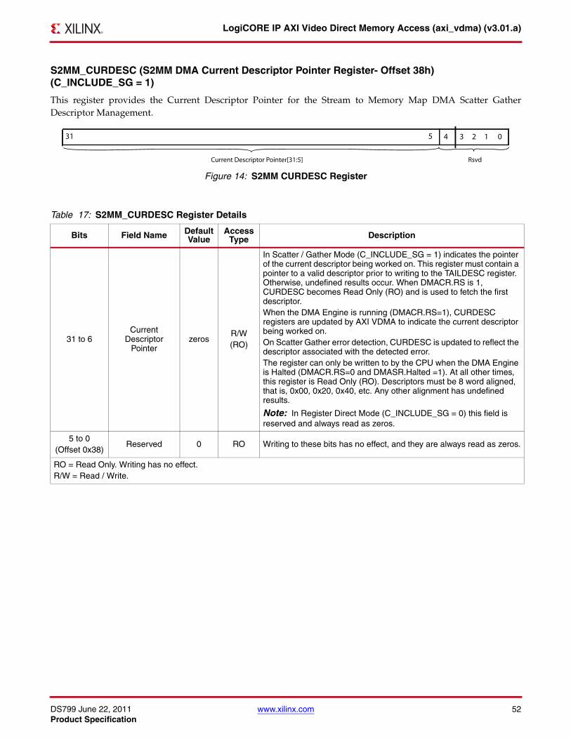
DS799 June 22, 2011 www.xilinx.com 52Product Specification
LogiCORE IP AXI Video Direct Memory Access (axi_vdma) (v3.01.a)
S2MM_CURDESC (S2MM DMA Current Descriptor Pointer Register- Offset 38h) (C_INCLUDE_SG = 1)
This register provides the Current Descriptor Pointer for the Stream to Memory Map DMA Scatter GatherDescriptor Management.X-Ref Target - Figure 14
Figure 14: S2MM CURDESC Register
Table 17: S2MM_CURDESC Register Details
Bits Field Name Default Value
Access Type Description
31 to 6Current
Descriptor Pointer
zerosR/W(RO)
In Scatter / Gather Mode (C_INCLUDE_SG = 1) indicates the pointer of the current descriptor being worked on. This register must contain a pointer to a valid descriptor prior to writing to the TAILDESC register. Otherwise, undefined results occur. When DMACR.RS is 1, CURDESC becomes Read Only (RO) and is used to fetch the first descriptor. When the DMA Engine is running (DMACR.RS=1), CURDESC registers are updated by AXI VDMA to indicate the current descriptor being worked on. On Scatter Gather error detection, CURDESC is updated to reflect the descriptor associated with the detected error.The register can only be written to by the CPU when the DMA Engine is Halted (DMACR.RS=0 and DMASR.Halted =1). At all other times, this register is Read Only (RO). Descriptors must be 8 word aligned, that is, 0x00, 0x20, 0x40, etc. Any other alignment has undefined results.
Note: In Register Direct Mode (C_INCLUDE_SG = 0) this field is reserved and always read as zeros.
5 to 0(Offset 0x38)
Reserved 0 RO Writing to these bits has no effect, and they are always read as zeros.
RO = Read Only. Writing has no effect.R/W = Read / Write.
31 5 4 3 2 1 0
Current Descriptor Pointer[31:5] Rsvd
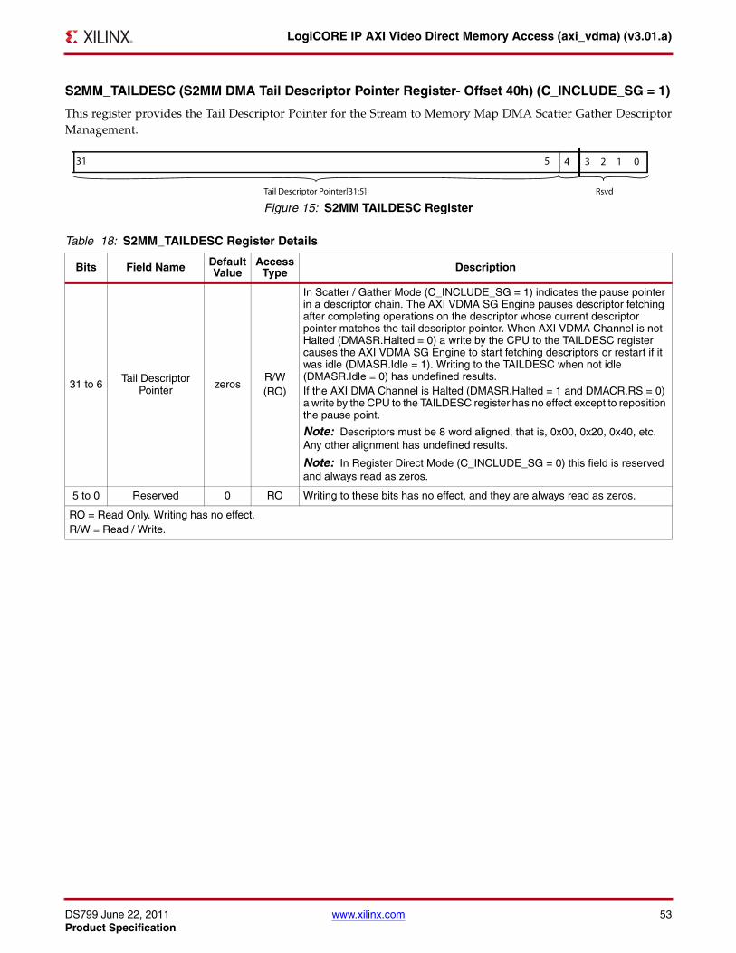
DS799 June 22, 2011 www.xilinx.com 53Product Specification
LogiCORE IP AXI Video Direct Memory Access (axi_vdma) (v3.01.a)
S2MM_TAILDESC (S2MM DMA Tail Descriptor Pointer Register- Offset 40h) (C_INCLUDE_SG = 1)
This register provides the Tail Descriptor Pointer for the Stream to Memory Map DMA Scatter Gather DescriptorManagement.X-Ref Target - Figure 15
Figure 15: S2MM TAILDESC Register
Table 18: S2MM_TAILDESC Register Details
Bits Field Name Default Value
Access Type Description
31 to 6 Tail Descriptor Pointer zeros
R/W(RO)
In Scatter / Gather Mode (C_INCLUDE_SG = 1) indicates the pause pointer in a descriptor chain. The AXI VDMA SG Engine pauses descriptor fetching after completing operations on the descriptor whose current descriptor pointer matches the tail descriptor pointer. When AXI VDMA Channel is not Halted (DMASR.Halted = 0) a write by the CPU to the TAILDESC register causes the AXI VDMA SG Engine to start fetching descriptors or restart if it was idle (DMASR.Idle = 1). Writing to the TAILDESC when not idle (DMASR.Idle = 0) has undefined results.If the AXI DMA Channel is Halted (DMASR.Halted = 1 and DMACR.RS = 0) a write by the CPU to the TAILDESC register has no effect except to reposition the pause point.
Note: Descriptors must be 8 word aligned, that is, 0x00, 0x20, 0x40, etc. Any other alignment has undefined results.
Note: In Register Direct Mode (C_INCLUDE_SG = 0) this field is reserved and always read as zeros.
5 to 0 Reserved 0 RO Writing to these bits has no effect, and they are always read as zeros.
RO = Read Only. Writing has no effect.R/W = Read / Write.
31 5 4 3 2 1 0
Tail Descriptor Pointer[31:5] Rsvd
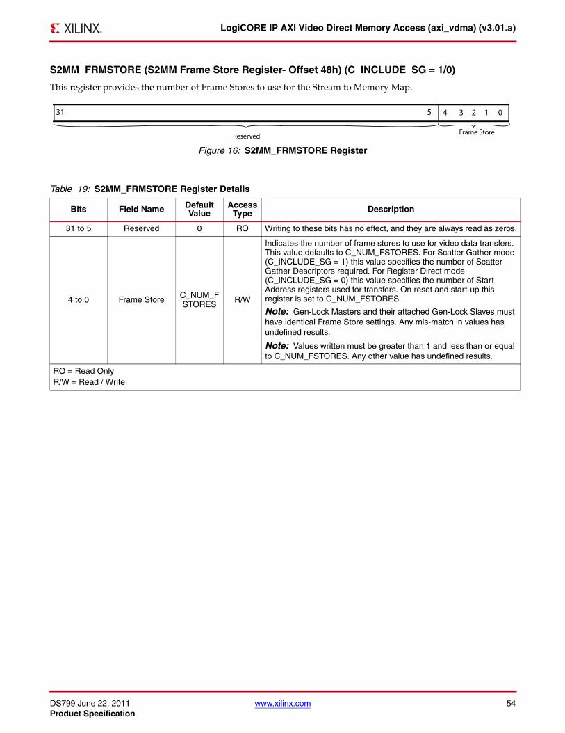
DS799 June 22, 2011 www.xilinx.com 54Product Specification
LogiCORE IP AXI Video Direct Memory Access (axi_vdma) (v3.01.a)
S2MM_FRMSTORE (S2MM Frame Store Register- Offset 48h) (C_INCLUDE_SG = 1/0)
This register provides the number of Frame Stores to use for the Stream to Memory Map.X-Ref Target - Figure 16
Figure 16: S2MM_FRMSTORE Register
Table 19: S2MM_FRMSTORE Register Details
Bits Field Name Default Value
Access Type Description
31 to 5 Reserved 0 RO Writing to these bits has no effect, and they are always read as zeros.
4 to 0 Frame Store C_NUM_FSTORES R/W
Indicates the number of frame stores to use for video data transfers. This value defaults to C_NUM_FSTORES. For Scatter Gather mode (C_INCLUDE_SG = 1) this value specifies the number of Scatter Gather Descriptors required. For Register Direct mode (C_INCLUDE_SG = 0) this value specifies the number of Start Address registers used for transfers. On reset and start-up this register is set to C_NUM_FSTORES.
Note: Gen-Lock Masters and their attached Gen-Lock Slaves must have identical Frame Store settings. Any mis-match in values has undefined results.
Note: Values written must be greater than 1 and less than or equal to C_NUM_FSTORES. Any other value has undefined results.
RO = Read OnlyR/W = Read / Write
31 5 4 3 2 1 0
ReservedFrame Store
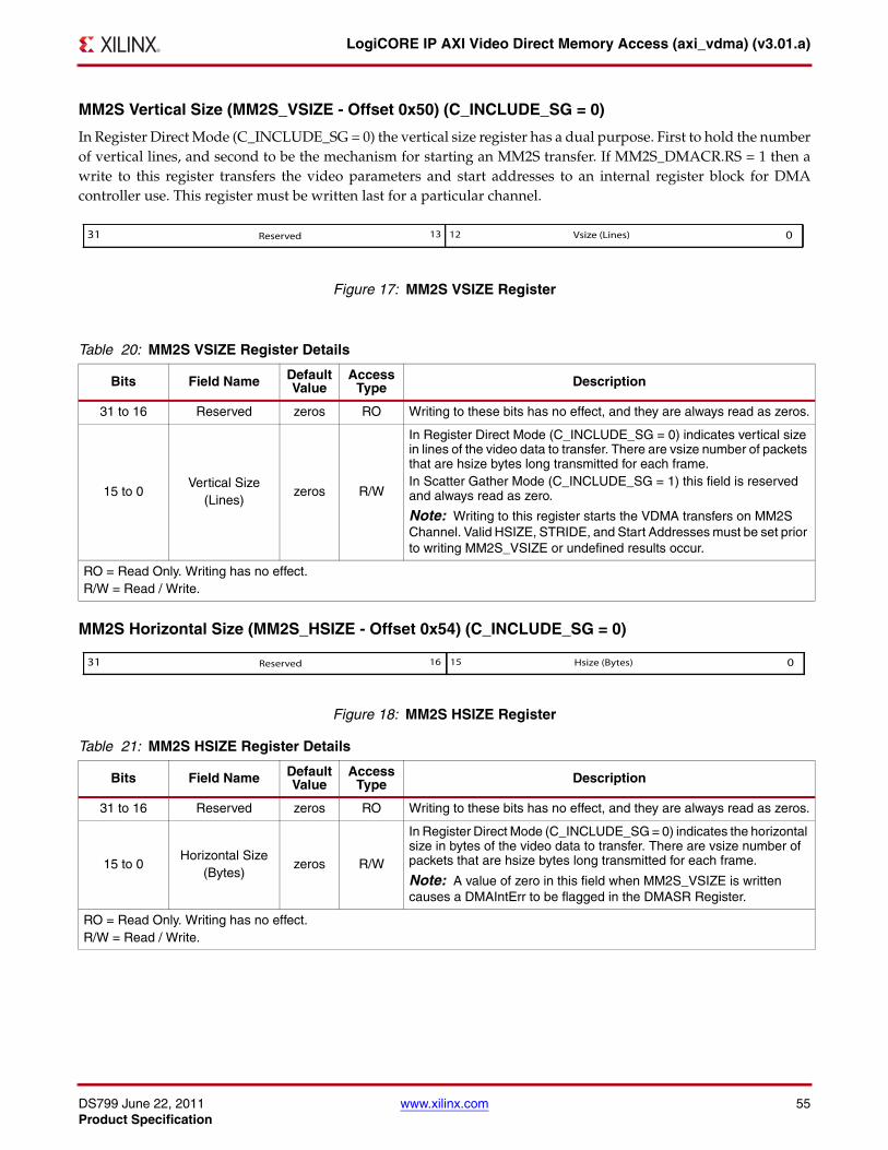
DS799 June 22, 2011 www.xilinx.com 55Product Specification
LogiCORE IP AXI Video Direct Memory Access (axi_vdma) (v3.01.a)
MM2S Vertical Size (MM2S_VSIZE - Offset 0x50) (C_INCLUDE_SG = 0)
In Register Direct Mode (C_INCLUDE_SG = 0) the vertical size register has a dual purpose. First to hold the numberof vertical lines, and second to be the mechanism for starting an MM2S transfer. If MM2S_DMACR.RS = 1 then awrite to this register transfers the video parameters and start addresses to an internal register block for DMAcontroller use. This register must be written last for a particular channel.
MM2S Horizontal Size (MM2S_HSIZE - Offset 0x54) (C_INCLUDE_SG = 0)
X-Ref Target - Figure 17
Figure 17: MM2S VSIZE Register
Table 20: MM2S VSIZE Register Details
Bits Field Name Default Value
Access Type Description
31 to 16 Reserved zeros RO Writing to these bits has no effect, and they are always read as zeros.
15 to 0Vertical Size
(Lines)zeros R/W
In Register Direct Mode (C_INCLUDE_SG = 0) indicates vertical size in lines of the video data to transfer. There are vsize number of packets that are hsize bytes long transmitted for each frame.In Scatter Gather Mode (C_INCLUDE_SG = 1) this field is reserved and always read as zero.
Note: Writing to this register starts the VDMA transfers on MM2S Channel. Valid HSIZE, STRIDE, and Start Addresses must be set prior to writing MM2S_VSIZE or undefined results occur.
RO = Read Only. Writing has no effect.R/W = Read / Write.
X-Ref Target - Figure 18
Figure 18: MM2S HSIZE Register
Table 21: MM2S HSIZE Register Details
Bits Field Name Default Value
Access Type Description
31 to 16 Reserved zeros RO Writing to these bits has no effect, and they are always read as zeros.
15 to 0Horizontal Size
(Bytes)zeros R/W
In Register Direct Mode (C_INCLUDE_SG = 0) indicates the horizontal size in bytes of the video data to transfer. There are vsize number of packets that are hsize bytes long transmitted for each frame.
Note: A value of zero in this field when MM2S_VSIZE is written causes a DMAIntErr to be flagged in the DMASR Register.
RO = Read Only. Writing has no effect.R/W = Read / Write.
31 013 12Reserved Vsize (Lines)
31 0Reserved Hsize (Bytes)16 15
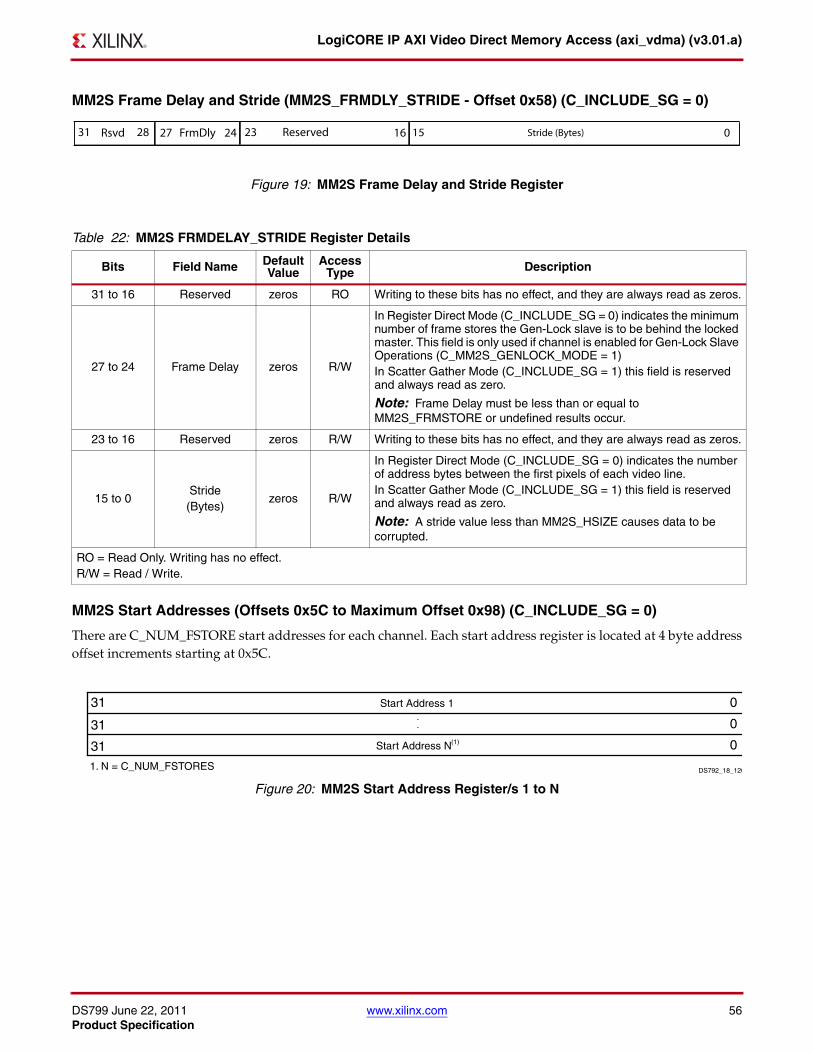
DS799 June 22, 2011 www.xilinx.com 56Product Specification
LogiCORE IP AXI Video Direct Memory Access (axi_vdma) (v3.01.a)
MM2S Frame Delay and Stride (MM2S_FRMDLY_STRIDE - Offset 0x58) (C_INCLUDE_SG = 0)
MM2S Start Addresses (Offsets 0x5C to Maximum Offset 0x98) (C_INCLUDE_SG = 0)
There are C_NUM_FSTORE start addresses for each channel. Each start address register is located at 4 byte addressoffset increments starting at 0x5C.
X-Ref Target - Figure 19
Figure 19: MM2S Frame Delay and Stride Register
Table 22: MM2S FRMDELAY_STRIDE Register Details
Bits Field Name Default Value
Access Type Description
31 to 16 Reserved zeros RO Writing to these bits has no effect, and they are always read as zeros.
27 to 24 Frame Delay zeros R/W
In Register Direct Mode (C_INCLUDE_SG = 0) indicates the minimum number of frame stores the Gen-Lock slave is to be behind the locked master. This field is only used if channel is enabled for Gen-Lock Slave Operations (C_MM2S_GENLOCK_MODE = 1)In Scatter Gather Mode (C_INCLUDE_SG = 1) this field is reserved and always read as zero.
Note: Frame Delay must be less than or equal to MM2S_FRMSTORE or undefined results occur.
23 to 16 Reserved zeros R/W Writing to these bits has no effect, and they are always read as zeros.
15 to 0Stride(Bytes)
zeros R/W
In Register Direct Mode (C_INCLUDE_SG = 0) indicates the number of address bytes between the first pixels of each video line.In Scatter Gather Mode (C_INCLUDE_SG = 1) this field is reserved and always read as zero.
Note: A stride value less than MM2S_HSIZE causes data to be corrupted.
RO = Read Only. Writing has no effect.R/W = Read / Write.
X-Ref Target - Figure 20
Figure 20: MM2S Start Address Register/s 1 to N
31 0Stride (Bytes)16 1528 27 23Rsvd FrmDly 24 Reserved
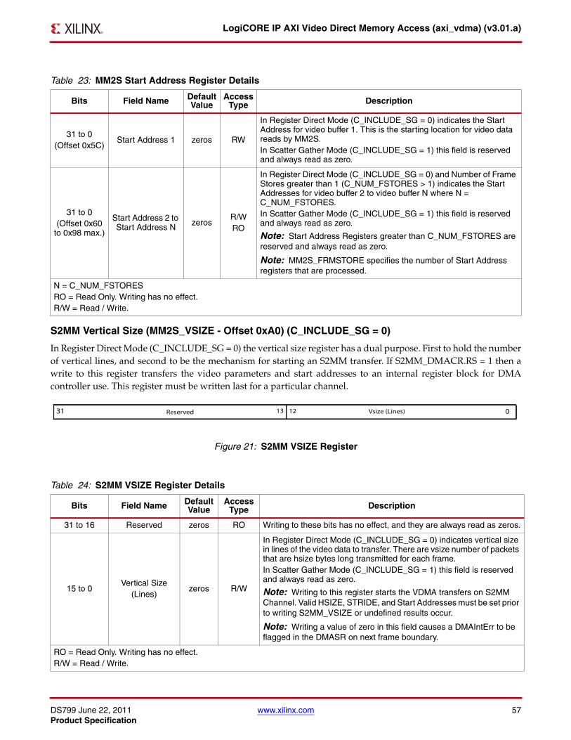
DS799 June 22, 2011 www.xilinx.com 57Product Specification
LogiCORE IP AXI Video Direct Memory Access (axi_vdma) (v3.01.a)
S2MM Vertical Size (MM2S_VSIZE - Offset 0xA0) (C_INCLUDE_SG = 0)
In Register Direct Mode (C_INCLUDE_SG = 0) the vertical size register has a dual purpose. First to hold the numberof vertical lines, and second to be the mechanism for starting an S2MM transfer. If S2MM_DMACR.RS = 1 then awrite to this register transfers the video parameters and start addresses to an internal register block for DMAcontroller use. This register must be written last for a particular channel.
Table 23: MM2S Start Address Register Details
Bits Field Name Default Value
Access Type Description
31 to 0(Offset 0x5C)
Start Address 1 zeros RW
In Register Direct Mode (C_INCLUDE_SG = 0) indicates the Start Address for video buffer 1. This is the starting location for video data reads by MM2S.In Scatter Gather Mode (C_INCLUDE_SG = 1) this field is reserved and always read as zero.
31 to 0(Offset 0x60
to 0x98 max.)
Start Address 2 to Start Address N zeros
R/WRO
In Register Direct Mode (C_INCLUDE_SG = 0) and Number of Frame Stores greater than 1 (C_NUM_FSTORES > 1) indicates the Start Addresses for video buffer 2 to video buffer N where N = C_NUM_FSTORES.In Scatter Gather Mode (C_INCLUDE_SG = 1) this field is reserved and always read as zero.
Note: Start Address Registers greater than C_NUM_FSTORES are reserved and always read as zero.
Note: MM2S_FRMSTORE specifies the number of Start Address registers that are processed.
N = C_NUM_FSTORESRO = Read Only. Writing has no effect.R/W = Read / Write.
X-Ref Target - Figure 21
Figure 21: S2MM VSIZE Register
Table 24: S2MM VSIZE Register Details
Bits Field Name Default Value
Access Type Description
31 to 16 Reserved zeros RO Writing to these bits has no effect, and they are always read as zeros.
15 to 0Vertical Size
(Lines)zeros R/W
In Register Direct Mode (C_INCLUDE_SG = 0) indicates vertical size in lines of the video data to transfer. There are vsize number of packets that are hsize bytes long transmitted for each frame.In Scatter Gather Mode (C_INCLUDE_SG = 1) this field is reserved and always read as zero.
Note: Writing to this register starts the VDMA transfers on S2MM Channel. Valid HSIZE, STRIDE, and Start Addresses must be set prior to writing S2MM_VSIZE or undefined results occur.
Note: Writing a value of zero in this field causes a DMAIntErr to be flagged in the DMASR on next frame boundary.
RO = Read Only. Writing has no effect.R/W = Read / Write.
31 013 12Reserved Vsize (Lines)
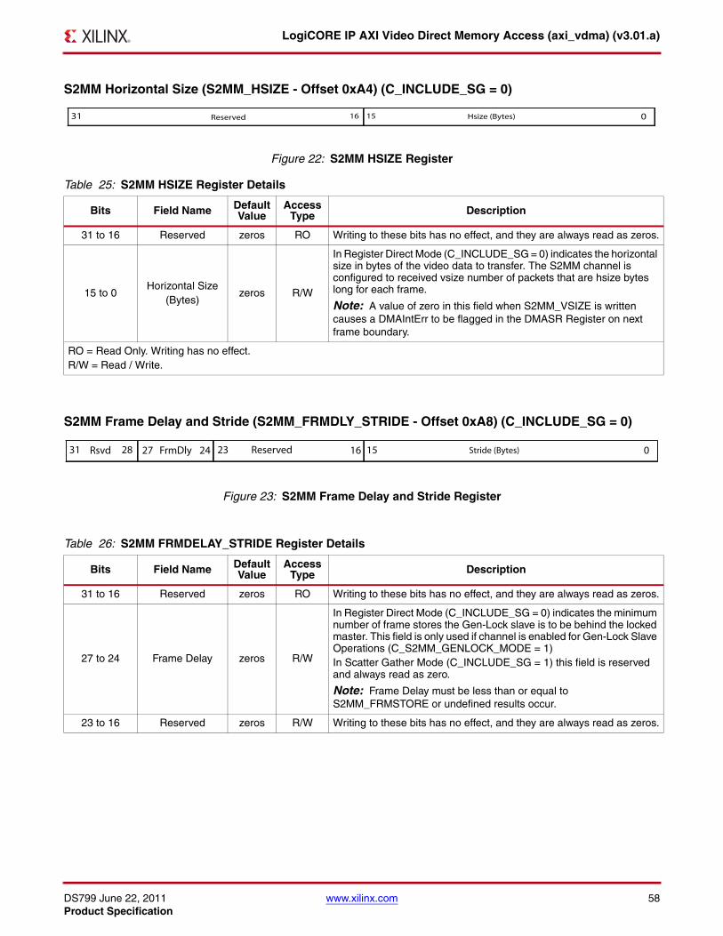
DS799 June 22, 2011 www.xilinx.com 58Product Specification
LogiCORE IP AXI Video Direct Memory Access (axi_vdma) (v3.01.a)
S2MM Horizontal Size (S2MM_HSIZE - Offset 0xA4) (C_INCLUDE_SG = 0)
S2MM Frame Delay and Stride (S2MM_FRMDLY_STRIDE - Offset 0xA8) (C_INCLUDE_SG = 0)
X-Ref Target - Figure 22
Figure 22: S2MM HSIZE Register
Table 25: S2MM HSIZE Register Details
Bits Field Name Default Value
Access Type Description
31 to 16 Reserved zeros RO Writing to these bits has no effect, and they are always read as zeros.
15 to 0Horizontal Size
(Bytes)zeros R/W
In Register Direct Mode (C_INCLUDE_SG = 0) indicates the horizontal size in bytes of the video data to transfer. The S2MM channel is configured to received vsize number of packets that are hsize bytes long for each frame.
Note: A value of zero in this field when S2MM_VSIZE is written causes a DMAIntErr to be flagged in the DMASR Register on next frame boundary.
RO = Read Only. Writing has no effect.R/W = Read / Write.
X-Ref Target - Figure 23
Figure 23: S2MM Frame Delay and Stride Register
Table 26: S2MM FRMDELAY_STRIDE Register Details
Bits Field Name Default Value
Access Type Description
31 to 16 Reserved zeros RO Writing to these bits has no effect, and they are always read as zeros.
27 to 24 Frame Delay zeros R/W
In Register Direct Mode (C_INCLUDE_SG = 0) indicates the minimum number of frame stores the Gen-Lock slave is to be behind the locked master. This field is only used if channel is enabled for Gen-Lock Slave Operations (C_S2MM_GENLOCK_MODE = 1)In Scatter Gather Mode (C_INCLUDE_SG = 1) this field is reserved and always read as zero.
Note: Frame Delay must be less than or equal to S2MM_FRMSTORE or undefined results occur.
23 to 16 Reserved zeros R/W Writing to these bits has no effect, and they are always read as zeros.
31 0Reserved Hsize (Bytes)16 15
31 0Stride (Bytes)16 1528 27 23Rsvd FrmDly 24 Reserved
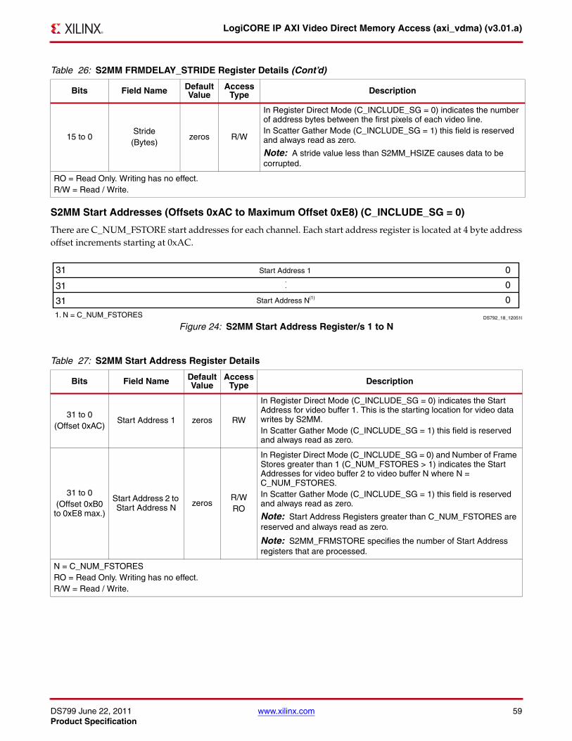
DS799 June 22, 2011 www.xilinx.com 59Product Specification
LogiCORE IP AXI Video Direct Memory Access (axi_vdma) (v3.01.a)
S2MM Start Addresses (Offsets 0xAC to Maximum Offset 0xE8) (C_INCLUDE_SG = 0)
There are C_NUM_FSTORE start addresses for each channel. Each start address register is located at 4 byte addressoffset increments starting at 0xAC.
15 to 0Stride(Bytes)
zeros R/W
In Register Direct Mode (C_INCLUDE_SG = 0) indicates the number of address bytes between the first pixels of each video line.In Scatter Gather Mode (C_INCLUDE_SG = 1) this field is reserved and always read as zero.
Note: A stride value less than S2MM_HSIZE causes data to be corrupted.
RO = Read Only. Writing has no effect.R/W = Read / Write.
X-Ref Target - Figure 24
Figure 24: S2MM Start Address Register/s 1 to N
Table 27: S2MM Start Address Register Details
Bits Field Name Default Value
Access Type Description
31 to 0(Offset 0xAC)
Start Address 1 zeros RW
In Register Direct Mode (C_INCLUDE_SG = 0) indicates the Start Address for video buffer 1. This is the starting location for video data writes by S2MM.In Scatter Gather Mode (C_INCLUDE_SG = 1) this field is reserved and always read as zero.
31 to 0(Offset 0xB0
to 0xE8 max.)
Start Address 2 to Start Address N zeros
R/WRO
In Register Direct Mode (C_INCLUDE_SG = 0) and Number of Frame Stores greater than 1 (C_NUM_FSTORES > 1) indicates the Start Addresses for video buffer 2 to video buffer N where N = C_NUM_FSTORES.In Scatter Gather Mode (C_INCLUDE_SG = 1) this field is reserved and always read as zero.
Note: Start Address Registers greater than C_NUM_FSTORES are reserved and always read as zero.
Note: S2MM_FRMSTORE specifies the number of Start Address registers that are processed.
N = C_NUM_FSTORESRO = Read Only. Writing has no effect.R/W = Read / Write.
Table 26: S2MM FRMDELAY_STRIDE Register Details (Cont’d)
Bits Field Name Default Value
Access Type Description
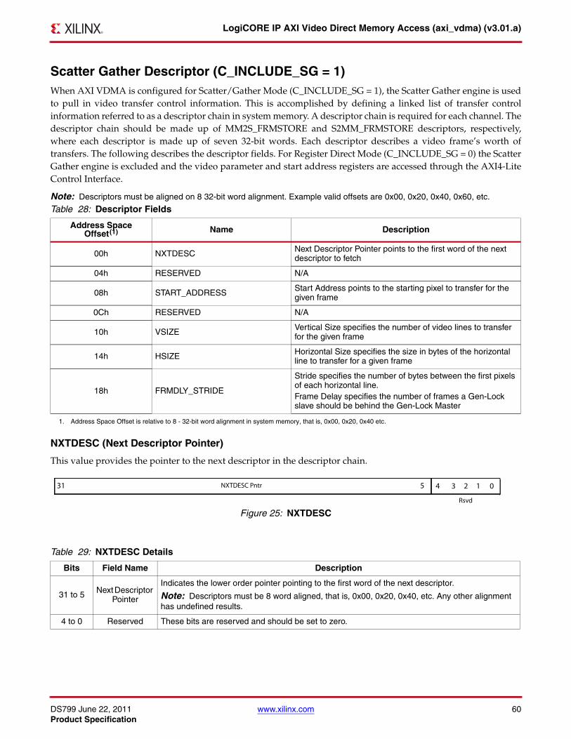
DS799 June 22, 2011 www.xilinx.com 60Product Specification
LogiCORE IP AXI Video Direct Memory Access (axi_vdma) (v3.01.a)
Scatter Gather Descriptor (C_INCLUDE_SG = 1)When AXI VDMA is configured for Scatter/Gather Mode (C_INCLUDE_SG = 1), the Scatter Gather engine is usedto pull in video transfer control information. This is accomplished by defining a linked list of transfer controlinformation referred to as a descriptor chain in system memory. A descriptor chain is required for each channel. Thedescriptor chain should be made up of MM2S_FRMSTORE and S2MM_FRMSTORE descriptors, respectively,where each descriptor is made up of seven 32-bit words. Each descriptor describes a video frame’s worth oftransfers. The following describes the descriptor fields. For Register Direct Mode (C_INCLUDE_SG = 0) the ScatterGather engine is excluded and the video parameter and start address registers are accessed through the AXI4-LiteControl Interface.
Note: Descriptors must be aligned on 8 32-bit word alignment. Example valid offsets are 0x00, 0x20, 0x40, 0x60, etc.
NXTDESC (Next Descriptor Pointer)
This value provides the pointer to the next descriptor in the descriptor chain.
Table 28: Descriptor Fields
Address Space Offset(1)
1. Address Space Offset is relative to 8 - 32-bit word alignment in system memory, that is, 0x00, 0x20, 0x40 etc.
Name Description
00h NXTDESC Next Descriptor Pointer points to the first word of the next descriptor to fetch
04h RESERVED N/A
08h START_ADDRESS Start Address points to the starting pixel to transfer for the given frame
0Ch RESERVED N/A
10h VSIZE Vertical Size specifies the number of video lines to transfer for the given frame
14h HSIZE Horizontal Size specifies the size in bytes of the horizontal line to transfer for a given frame
18h FRMDLY_STRIDE
Stride specifies the number of bytes between the first pixels of each horizontal line.Frame Delay specifies the number of frames a Gen-Lock slave should be behind the Gen-Lock Master
X-Ref Target - Figure 25
Figure 25: NXTDESC
Table 29: NXTDESC Details
Bits Field Name Description
31 to 5 Next Descriptor Pointer
Indicates the lower order pointer pointing to the first word of the next descriptor.
Note: Descriptors must be 8 word aligned, that is, 0x00, 0x20, 0x40, etc. Any other alignment has undefined results.
4 to 0 Reserved These bits are reserved and should be set to zero.
31 5 4 3 2 1 0NXTDESC Pntr
Rsvd
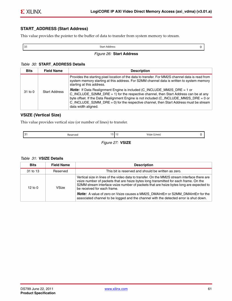
DS799 June 22, 2011 www.xilinx.com 61Product Specification
LogiCORE IP AXI Video Direct Memory Access (axi_vdma) (v3.01.a)
START_ADDRESS (Start Address)
This value provides the pointer to the buffer of data to transfer from system memory to stream.
VSIZE (Vertical Size)
This value provides vertical size (or number of lines) to transfer.
X-Ref Target - Figure 26
Figure 26: Start Address
Table 30: START_ADDRESS Details
Bits Field Name Description
31 to 0 Start Address
Provides the starting pixel location of the data to transfer. For MM2S channel data is read from system memory starting at this address. For S2MM channel data is written to system memory starting at this address.
Note: If Data Realignment Engine is included (C_INCLUDE_MM2S_DRE = 1 or C_INCLUDE_S2MM_DRE = 1) for the respective channel, then Start Address can be at any byte offset. If the Data Realignment Engine is not included (C_INCLUDE_MM2S_DRE = 0 or C_INCLUDE_S2MM_DRE = 0) for the respective channel, then Start Address must be stream data width aligned.
X-Ref Target - Figure 27
Figure 27: VSIZE
Table 31: VSIZE Details
Bits Field Name Description
31 to 13 Reserved This bit is reserved and should be written as zero.
12 to 0 VSize
Vertical size in lines of the video data to transfer. On the MM2S stream interface there are vsize number of packets that are hsize bytes long transmitted for each frame. On the S2MM stream interface vsize number of packets that are hsize bytes long are expected to be received for each frame.
Note: A value of zero on Vsize causes a MM2S_DMAIntErr or S2MM_DMAIntErr for the associated channel to be logged and the channel with the detected error is shut down.
31 0Start Address
31 013 12Reserved Vsize (Lines)
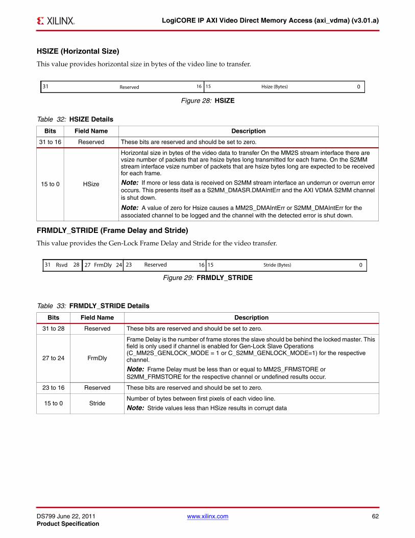
DS799 June 22, 2011 www.xilinx.com 62Product Specification
LogiCORE IP AXI Video Direct Memory Access (axi_vdma) (v3.01.a)
HSIZE (Horizontal Size)
This value provides horizontal size in bytes of the video line to transfer.
FRMDLY_STRIDE (Frame Delay and Stride)
This value provides the Gen-Lock Frame Delay and Stride for the video transfer.
X-Ref Target - Figure 28
Figure 28: HSIZE
Table 32: HSIZE Details
Bits Field Name Description
31 to 16 Reserved These bits are reserved and should be set to zero.
15 to 0 HSize
Horizontal size in bytes of the video data to transfer On the MM2S stream interface there are vsize number of packets that are hsize bytes long transmitted for each frame. On the S2MM stream interface vsize number of packets that are hsize bytes long are expected to be received for each frame.
Note: If more or less data is received on S2MM stream interface an underrun or overrun error occurs. This presents itself as a S2MM_DMASR.DMAIntErr and the AXI VDMA S2MM channel is shut down.
Note: A value of zero for Hsize causes a MM2S_DMAIntErr or S2MM_DMAIntErr for the associated channel to be logged and the channel with the detected error is shut down.
X-Ref Target - Figure 29
Figure 29: FRMDLY_STRIDE
Table 33: FRMDLY_STRIDE Details
Bits Field Name Description
31 to 28 Reserved These bits are reserved and should be set to zero.
27 to 24 FrmDly
Frame Delay is the number of frame stores the slave should be behind the locked master. This field is only used if channel is enabled for Gen-Lock Slave Operations (C_MM2S_GENLOCK_MODE = 1 or C_S2MM_GENLOCK_MODE=1) for the respective channel.
Note: Frame Delay must be less than or equal to MM2S_FRMSTORE or S2MM_FRMSTORE for the respective channel or undefined results occur.
23 to 16 Reserved These bits are reserved and should be set to zero.
15 to 0 StrideNumber of bytes between first pixels of each video line.
Note: Stride values less than HSize results in corrupt data
31 0Reserved Hsize (Bytes)16 15
31 0Stride (Bytes)16 1528 27 23Rsvd FrmDly 24 Reserved
DS799 June 22, 2011 www.xilinx.com 63Product Specification
LogiCORE IP AXI Video Direct Memory Access (axi_vdma) (v3.01.a)
AXI VDMA OperationThere are two major modes of operation, Scatter/Gather Mode and Register Direct Mode. The followingparagraphs describe AXI VDMA operations for both modes.
Scatter / Gather Operation Mode (C_INCLUDE_SG = 1)
AXI VDMA Operation requires a memory-resident data structure that holds the list of DMA operations to beperformed. This list of instructions is organized into what is referred to as a descriptor chain. Each descriptor has apointer to the next descriptor to be processed. The last descriptor in the chain then points back to the first descriptorin the chain.
VDMA operations began with the set up of the descriptor pointer registers and the DMA control registers. Thefollowing lists minimum steps, in order, required for AXI VDMA operations:
1. Write a valid pointer to the channel’s CURDESC_PNTR register (Offset 0x08 for MM2S and 0x38 for S2MM).
2. Write control information to channel’s DMACR register (Offset 0x00 for MM2S and 0x30 for S2MM) to set interrupt enables if desired, frame count, delay count if desired, and set DMACR.RS=1 to start the AXI VDMA channel running. There can be a lag between when the CPU sets DMACR.RS=1 and when AXI VDMA sets DMASR.Halted = 0. The CPU can determine if the AXI VDMA is running when DMACR.RS = 1 and DMASR.Halted = 0.
3. Write a valid point to the channel’s TAILDESC_PNTR register (Offset 0x10 for MM2S and 0x40 for S2MM). This starts the channel fetching and processing descriptors.
4. DMA scatter gather operations continue until the descriptor at TAILDESC_PNTR is processed, then the engine idles as indicated by DMASR.Idle = 1.
The descriptor chain is made up of a maximum of C_NUM_FSTORES descriptors per channel. The SG Enginefetches descriptors and update an internal register set with the descriptor information (See Example Figure 30). Thevideo timing information (vsize, hsize, stride, and frame delay) from the first descriptor fetched after theTAILDESC pointer is written by the CPU is captured and stored. This video timing information is used for alltransfers in all frames for the specified channel. All other video timing information in the other descriptors areignored by the AXI VDMA. Start Addresses from each descriptor are populated into C_NUM_FSTORES internaladdress registers.
When the SG Engine reaches the descriptor pointed to by TAILDESC, the SG Engine processes that descriptor, setthe internal register set to ping-pong on the next frame sync (Internally generated if C_USE_FSYNC = 0 orexternally if C_USE_FSYNC = 1), and enter an Idle state. At the next frame sync the internal register set will switchsuch that the DMA controller operates on the newly updated values.
This method for handling data updates internally allows the SG engine to operate on a register set without steppingon the register set that the DMA controller is using for data transfers. It also allows the SG Engine to only fetchdescriptors when a change is made to the data set making it unnecessary for the SG engine to fetch a descriptor witheach frame. It should be noted that the DMA controller continues to transfer video data even though the SG enginehas reached the tail pointer and paused. This allows un-interrupted video data transfers.
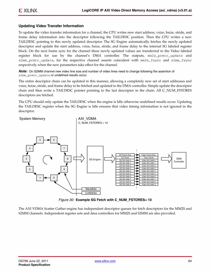
DS799 June 22, 2011 www.xilinx.com 64Product Specification
LogiCORE IP AXI Video Direct Memory Access (axi_vdma) (v3.01.a)
Updating Video Transfer Information
To update the video transfer information for a channel, the CPU writes new start address, vsize, hsize, stride, andframe delay information into the descriptor following the TAILDESC position. Then the CPU writes a newTAILDESC pointing to this newly updated descriptor. The SG Engine automatically fetches the newly updateddescriptor and update the start address, vsize, hsize, stride, and frame delay to the internal SG labeled registerblock. On the next frame sync for the channel these newly updated values are transferred to the Video labeledregister block for use by the channel’s DMA controller. The outputs, mm2s_prmtr_update ands2mm_prmtr_update, for the respective channel asserts coincident with mm2s_fsync and s2mm_fsyncrespectively when the new parameters take effect for the channel.
Note: On S2MM channel new video line size and number of video lines need to change following the assertion of s2mm_prmtr_update or undefined results occur.
The entire descriptor chain can be updated in this manner, allowing a completely new set of start addresses andvsize, hsize, stride, and frame delay to be fetched and updated to the DMA controller. Simple update the descriptorchain and then write a TAILDESC pointer pointing to the last descriptor in the chain. All C_NUM_FSTORESdescriptors are fetched.
The CPU should only update the TAILDESC when the engine is Idle otherwise undefined results occur. Updatingthe TAILDESC register when the SG Engine is Idle ensures that video timing information is not ignored in thedescriptor.
The AXI VDMA Scatter Gather engine has independent descriptor queues for fetch descriptors for the MM2S andS2MM channels. Independent register sets and dma controllers for MM2S and S2MM are also provided.
X-Ref Target - Figure 30
Figure 30: Example SG Fetch with C_NUM_FSTORES= 10
3
4
5 6
7
8
2
1 0
9
AXI_VDMAC_NUM_FSTORES = 10
CURDESC
TAILDESC
SG Engine
SG Frame Size
SG Stride
SG Strt Addr 0
SG Strt Addr 9
Video Frame Size
Video Stride DMA Controller
SG Strt Addr 5
SG Strt Addr 4
SG Strt Addr 3
SG Strt Addr 2
SG Strt Addr 1
SG Strt Addr 6
SG Strt Addr 7
SG Strt Addr 8
Video Strt Addr 0
Video Strt Addr 5
Video Strt Addr 4
Video Strt Addr 3
Video Strt Addr 2
Video Strt Addr 1
Video Strt Addr 6
Video Strt Addr 7
Video Strt Addr 8
Video Strt Addr 9
System Memory
DS799 June 22, 2011 www.xilinx.com 65Product Specification
LogiCORE IP AXI Video Direct Memory Access (axi_vdma) (v3.01.a)
Register Direct Mode Operations (C_INCLUDE_SG = 0)
For operations without a scatter gather engine, an expanded AXI4-Lite register map is provided, exposing the videospecific register fields to read and write via the AXI4-Lite Interface (See Figure 2 and Table 7). These registersinclude the DMACR, DMASR, PART_PTR_REG, VIDEO_VERSION, VSIZE, HSIZE, FRMDLY_STRIDE, andSTART ADDRESS/ES for each respective channel. Some applications for Register Direct mode include systems thatdo not have a CPU.
VDMA operations in register direct mode begin with the set up of the video parameter and start address registersand the DMA control registers. The following lists minimum steps, in order, required to start AXI VDMAoperations:
1. Write control information to channel’s DMACR register (Offset 0x00 for MM2S and 0x30 for S2MM) to set interrupt enables if desired, frame count, delay count if desired, and set DMACR.RS=1 to start the AXI VDMA channel running. There can be a lag between when the CPU sets DMACR.RS=1 and when AXI VDMA sets DMASR.Halted = 0. The CPU can determine if the AXI VDMA is running when DMACR.RS = 1 and DMASR.Halted = 0.
2. Write valid video frame buffer start address to the channel’s START_ADDRESS register 1 to N where N equals C_NUM_FSTORES (Offset 058 up to 0x98 for MM2S and 0xAC up to 0xE8 for S2MM).
3. Write a valid Frame Delay and Stride to the channel’s FRMDLY_STRIDE register (Offset 0x58 for MM2S and 0xA8 for S2MM).
4. Write a valid Horizontal Size to the channel’s HSIZE register (Offset 0x54 for MM2S and 0xA4 for S2MM).
5. Finally write a valid Vertical Size to the channel’s VSIZE register (Offset 0x50 for MM2S and 0xA0 for S2MM). This start s the channel transferring video data.
Note: On S2MM channel new video line size and number of video lines need to change following the assertion of s2mm_prmtr_update or undefined results occur.
Updating Video Transfer Information
In Register Direct Mode (C_INCLUDE_SG = 0), the user is able to update video parameter settings at any timewhile the engine is running by writing new video parameters and video start address through the AXI4-Lite controlinterface. The newly written video transfer values take effect on the next frame boundary after the user writes thevertical size register for the respective channel. The channel’s pmrtr_update output (mm2s_prmtr_update ands2mm_prmtr_update) for the respective channel asserts indicating the new video parameters are being used bythe AXI VDMA.
To update video parameters dynamically while AXI VDMA operations are on going a similar process to the startsteps is needed.
1. Write the Frame Delay, Stride, and Horizontal Size in any order for the associated channel.
2. Finally, write the Vertical Size. When VSize is written the video register values are transferred to an internal register block. On the next frame boundary the DMA controller for the associated channel starts transfers using the newly updated values.
For applications where reading of the video parameters and start address registers is not needed, then FPGAresources can be reduced by excluding the read logic for the video specific registers (VSIZE, HSIZE,FRMDLY_STRIDE, and START ADDRESS/ES). This is accomplished by setting C_ENABLE_VIDPRMTR_READS= 0.
DS799 June 22, 2011 www.xilinx.com 66Product Specification
LogiCORE IP AXI Video Direct Memory Access (axi_vdma) (v3.01.a)
AXI VDMA General Operations
AXI VDMA Frame Boundary
A frame boundary depends on the mode of operation. For external fsync mode (C_USE_FSYNC = 1) the frameboundary is based on the channel’s fsync input, mm2s_fsync or s2mm_fsync. AXI VDMA starts the transfer for aparticular frame after driving out an fsync_out for the associated channel (mm2s_fsync_out ors2mm_fsync_out). There is some pipeline delay between the fsync input and when fsync_out is driven.
For free run mode (C_USE_FSYNC = 0) an internal fsync is generated for timing transfers. AXI VDMA transfers thecommanded transfers as quickly as it is able to process and transfer the data. AXI VDMA will drive out anfsync_out for the associated channel, mm2s_fsync_out or s2mm_fsync_out, on each frame boundary.
In both free run and external fsync modes, on S2MM, AXI VDMA asserts s_axis_s2mm_tready afters2mm_fsync_out asserts indicating to the attached video IP that AXI VDMA is ready to accept data. At the end ofeach frame, when all expected data is received, the AXI VDMA deasserts s_axis_s2mm_tready until the start ofthe next frame as indicated by the assertion of s2mm_fsync_out.When new video parameters have been updated to AXI VDMA and the associated channel starts operating on thenew video parameters and start addresses, AXI VDMA asserts the associated channel prmtr_update,mm2s_prmtr_update or s2mm_prmtr_update, coincident with fsync_out for the associated channel. Thisindicates to the attached video IP that new line length, and or line number is in effect.
AXI VDMA Video Transfer
Data is transferred from System Memory to Stream or Stream to System Memory as defined by the Start Address forthe frame currently being operated on and the vertical size, horizontal size, and stride. Figure 31 illustrates a typicalvideo image stored in system memory. The smaller portion of the video image is to be transferred. Vertical Size linesof Horizontal Size number of bytes are transferred from or to system memory starting at each start address for eachvideo frame.
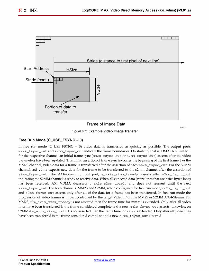
DS799 June 22, 2011 www.xilinx.com 67Product Specification
LogiCORE IP AXI Video Direct Memory Access (axi_vdma) (v3.01.a)
Free Run Mode (C_USE_FSYNC = 0)
In free run mode (C_USE_FSYNC = 0) video data is transferred as quickly as possible. The output portsmm2s_fsync_out and s2mm_fsync_out indicate the frame boundaries. On start-up, that is, DMACR.RS set to 1for the respective channel, an initial frame sync (mm2s_fsync_out or s2mm_fsync_out) asserts after the videoparameters have been updated. This initial assertion of frame sync indicates the beginning of the first frame. For theMM2S channel, video data for a frame is transferred after the assertion of each mm2s_fsync_out. For the S2MMchannel, axi_vdma expects new data for the frame to be transferred to the s2mm channel after the assertion ofs2mm_fsync_out. The AXI4-Stream output port, s_axis_s2mm_tready, asserts after s2mm_fsync_outindicating the S2MM channel is ready to receive data. When all expected data (vsize lines that are hsize bytes long)has been received, AXI VDMA deasserts s_axis_s2mm_tready and does not reassert until the nexts2mm_fsync_out. For both channels, MM2S and S2MM, when configured for free run mode, mm2s_fsync_outand s2mm_fsync_out asserts only after all of the data for a frame has been transferred. In free run mode theprogression of video frames is in part controlled by the target Video IP on the MM2S or S2MM AXI4-Stream. ForMM2S, if m_axis_mm2s_tready is not asserted then the frame time for mm2s is extended. Only after all videolines have been transferred is the frame considered complete and a new mm2s_fsync_out asserts. Likewise, onS2MM if s_axis_s2mm_tvalid is not asserted then the frame time for s2mm is extended. Only after all video lineshave been transferred is the frame considered complete and a new s2mm_fsync_out asserted.
X-Ref Target - Figure 31
Figure 31: Example Video Image Transfer
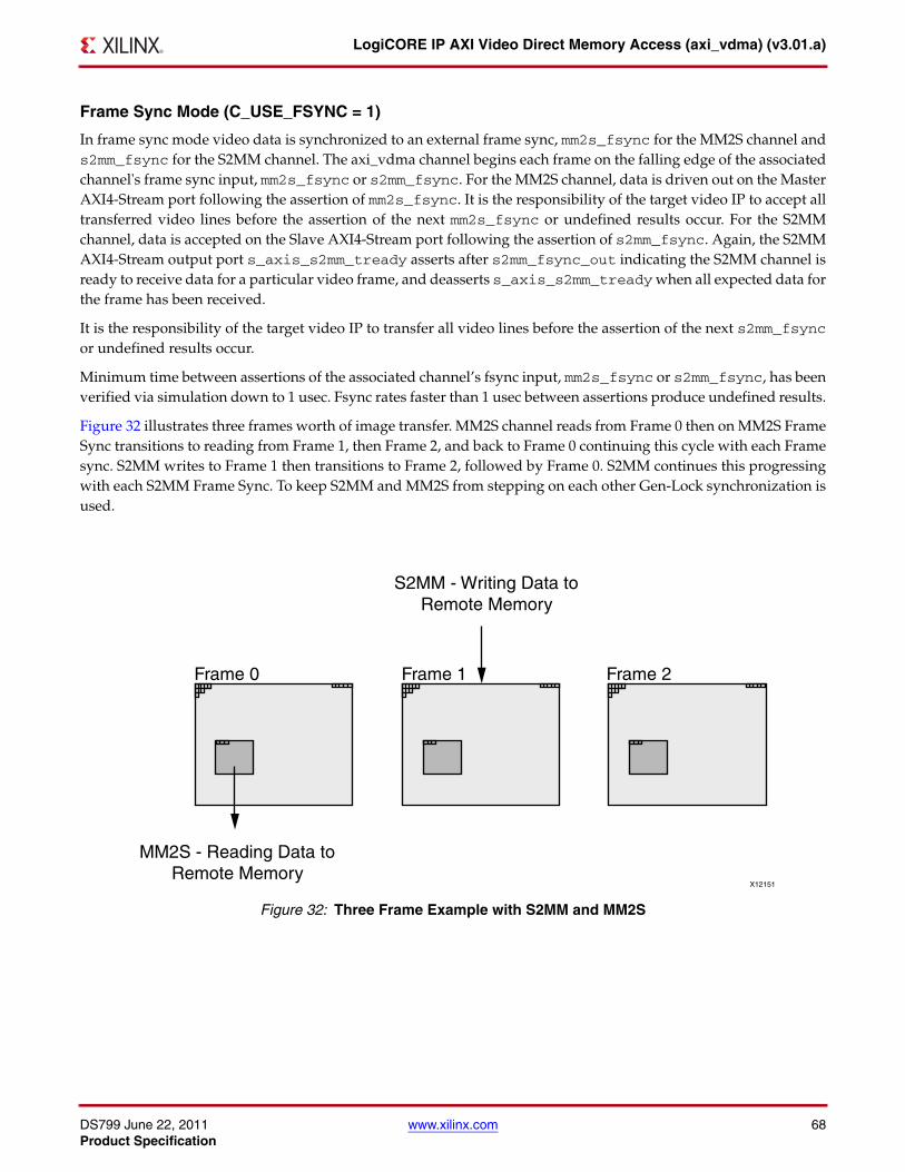
DS799 June 22, 2011 www.xilinx.com 68Product Specification
LogiCORE IP AXI Video Direct Memory Access (axi_vdma) (v3.01.a)
Frame Sync Mode (C_USE_FSYNC = 1)
In frame sync mode video data is synchronized to an external frame sync, mm2s_fsync for the MM2S channel ands2mm_fsync for the S2MM channel. The axi_vdma channel begins each frame on the falling edge of the associatedchannel's frame sync input, mm2s_fsync or s2mm_fsync. For the MM2S channel, data is driven out on the MasterAXI4-Stream port following the assertion of mm2s_fsync. It is the responsibility of the target video IP to accept alltransferred video lines before the assertion of the next mm2s_fsync or undefined results occur. For the S2MMchannel, data is accepted on the Slave AXI4-Stream port following the assertion of s2mm_fsync. Again, the S2MMAXI4-Stream output port s_axis_s2mm_tready asserts after s2mm_fsync_out indicating the S2MM channel isready to receive data for a particular video frame, and deasserts s_axis_s2mm_tready when all expected data forthe frame has been received.
It is the responsibility of the target video IP to transfer all video lines before the assertion of the next s2mm_fsyncor undefined results occur.
Minimum time between assertions of the associated channel’s fsync input, mm2s_fsync or s2mm_fsync, has beenverified via simulation down to 1 usec. Fsync rates faster than 1 usec between assertions produce undefined results.
Figure 32 illustrates three frames worth of image transfer. MM2S channel reads from Frame 0 then on MM2S FrameSync transitions to reading from Frame 1, then Frame 2, and back to Frame 0 continuing this cycle with each Framesync. S2MM writes to Frame 1 then transitions to Frame 2, followed by Frame 0. S2MM continues this progressingwith each S2MM Frame Sync. To keep S2MM and MM2S from stepping on each other Gen-Lock synchronization isused.
X-Ref Target - Figure 32
Figure 32: Three Frame Example with S2MM and MM2S
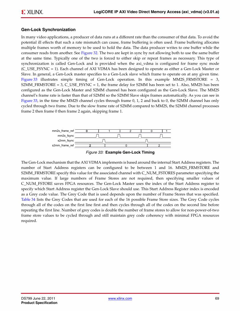
DS799 June 22, 2011 www.xilinx.com 69Product Specification
LogiCORE IP AXI Video Direct Memory Access (axi_vdma) (v3.01.a)
Gen-Lock Synchronization
In many video applications, a producer of data runs at a different rate than the consumer of that data. To avoid thepotential ill effects that such a rate mismatch can cause, frame buffering is often used. Frame buffering allocatesmultiple frames worth of memory to be used to hold the data. The data producer writes to one buffer while theconsumer reads from another. See Figure 32. The two are kept in sync by not allowing both to use the same bufferat the same time. Typically one of the two is forced to either skip or repeat frames as necessary. This type ofsynchronization is called Gen-Lock and is provided when the axi_vdma is configured for frame sync mode(C_USE_FSYNC = 1). Each channel of AXI VDMA has been designed to operate as either a Gen-Lock Master orSlave. In general, a Gen-Lock master specifies to a Gen-Lock slave which frame to operate on at any given time.Figure 33 illustrates simple timing of Gen-Lock operation. In this example MM2S_FRMSTORE = 3,S2MM_FRMSTORE = 3, C_USE_FSYNC = 1, the frame delay for S2MM has been set to 1. Also, MM2S has beenconfigured as the Gen-Lock Master and S2MM channel has been configured as the Gen-Lock Slave. The MM2Schannel’s frame rate is faster than that of S2MM so the S2MM Slave skips frames automatically. As you can see inFigure 33, in the time the MM2S channel cycles through frame 0, 1, 2 and back to 0, the S2MM channel has onlycycled through two frame. Due to the slow frame rate of S2MM compared to MM2S, the S2MM channel processesframe 2 then frame 0 then frame 2 again, skipping frame 1.
The Gen-Lock mechanism that the AXI VDMA implements is based around the internal Start Address registers. Thenumber of Start Address registers can be configured to be between 1 and 16. MM2S_FRMSTORE andS2MM_FRMSTORE specify this value for the associated channel with C_NUM_FSTORES parameter specifying themaximum value. If large numbers of Frame Stores are not required, then specifying smaller values ofC_NUM_FSTORE saves FPGA resources. The Gen-Lock Master uses the index of the Start Address register tospecify which Start Address register the Gen-Lock Slave should use. This Start Address Register index is encodedas a Grey code value. The Grey Code that is used depends upon the number of Frame Stores that was specified.Table 34 lists the Grey Codes that are used for each of the 16 possible Frame Store sizes. The Grey Code cyclesthrough all of the codes on the first line first and then cycles through all of the codes on the second line beforerepeating the first line. Number of grey codes is double the number of frame stores to allow for non-power-of-twoframe store values to be cycled through and still maintain grey code coherency with minimal FPGA resourcesrequired.
X-Ref Target - Figure 33
Figure 33: Example Gen-Lock Timing
mm2s_frame_ref
mm2s_fsync
s2mm_fsync
s2mm_frame_ref
00 1 2 0 1
22 0 2
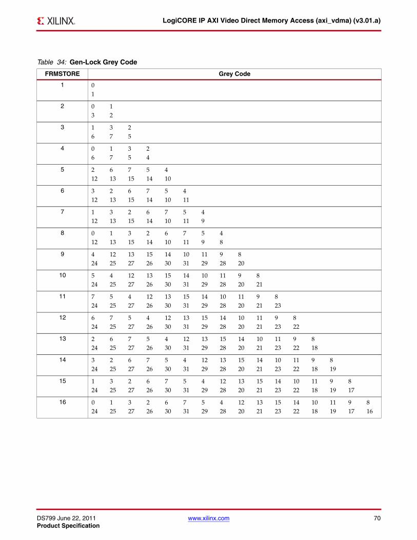
DS799 June 22, 2011 www.xilinx.com 70Product Specification
LogiCORE IP AXI Video Direct Memory Access (axi_vdma) (v3.01.a)
Table 34: Gen-Lock Grey Code
FRMSTORE Grey Code
1 01
2 03
12
3 16
37
25
4 06
17
35
24
5 212
613
715
514
410
6 312
213
615
714
510
411
7 112
313
215
614
710
511
49
8 012
113
315
214
610
711
59
48
9 424
1225
1327
1526
1430
1031
1129
928
820
10 524
425
1227
1326
1530
1431
1029
1128
920
821
11 724
525
427
1226
1330
1531
1429
1028
1120
921
823
12 624
725
527
426
1230
1331
1529
1428
1020
1121
923
822
13 224
625
727
526
430
1231
1329
1528
1420
1021
1123
922
818
14 324
225
627
726
530
431
1229
1328
1520
1421
1023
1122
918
819
15 124
325
227
626
730
531
429
1228
1320
1521
1423
1022
1118
919
817
16 024
125
327
226
630
731
529
428
1220
1321
1523
1422
1018
1119
917
816
DS799 June 22, 2011 www.xilinx.com 71Product Specification
LogiCORE IP AXI Video Direct Memory Access (axi_vdma) (v3.01.a)
The grey codes received by the Gen-Lock slave are then converted to a frame reference to tell the Gen-Lock slavewhich frame to work on. The slave modifies the Gen-Lock frame reference received by the frame delay such that theGen-Lock slaves remains Frame Delay behind the Gen-Lock Master. Table 35 illustrates an example conversionfrom Gen-Lock Grey Code to Frame Reference used by the Gen-Lock Slave.
Line Buffers
Optional line buffer can be utilized to prevent memory controller throttling from causing inner packet throttling onthe stream interface. Line buffer depth is configurable by the user (via C_MM2S_BUFFER_DEPTH andC_S2MM_BUFFER_DEPTH) to provide the necessary buffering for a specific video application. For transmit(MM2S), this line buffering presents several clocks of latency at the onset of a video frame transfer between systemmemory read and initial tvalid on AXI4-Stream as the line buffer queues up a portion of the data to transfer.
Line buffer status is provided for video IP use. mm2s_linebuffer_empty and mm2s_linebuffer_almost empty are provided for the MM2S channel and s2mm_linebuffer_full and s2mm_linebuffer_almost_full are provided for the S2MM channel. Threshold parameters are provided to specify the assertion points for mm2s_linebuffer_almost_empty and s2mm_linebuffer_almost_full.
For MM2S, C_MM2S_LINEBUFFER_THRESH specifies the assertion point for mm2s_buffer_almost_empty.The parameter is specified in bytes and must be a specified in even multiples of the MM2S AXIS data width in bytes(that is, C_M_AXIS_MM2S_TDATA_WIDTH / 8 multiples). mm2s_buffer_almost_empty asserts when thereare C_MM2S_LINEBUFFER_THRESH bytes or less, excluding 0 bytes, left in the Line Buffer. For example ifC_MM2S_LINE_BUFFER_THRESH = 8 then mm2s_buffer_almost empty asserts when the number of stored bytesis 8,7,6,5,4,3,2, or 1. When byte count = 0 then mm2s_buffer_almost_empty deasserts andmm2s_buffer_empty with assert.
To prevent throttling within a MM2S AXI4-Stream packet, the target Video IP is responsible for not assertingm_axis_mm2s_tready = 1 until mm2s_buffer_almost_empty deasserts and mm2s_buffer_empty = 0indicating more than C_MM2S_LINEBUFFER_THRESH data is stored in the line buffer. Adjustments might needto be made to the C_MM2S_LINEBUFFER_THRESH value for a user’s application to prevent throttling withinpackets.
For S2MM, C_S2MM_LINEBUFFER_THRESH specifies the assertion point of s2mm_buffer_almost_full. Theparameter is specified in bytes and must be specified in even multiples of the S2MM AXIS data width in bytes (thatis, C_S_AXIS_S2MM_TDATA_WIDTH / 8 multiples). s2mm_buffer_almost_full asserts when there areC_S2MM_LINEBUFFER_THRESH bytes or more in the Line Buffer. For example ifC_MM2S_LINEBUFFER_THRESH = 8 then s2mm_buffer_almost_full asserts when the number of storedbytes is 8 or greater. When line buffer is full then s2mm_buffer_almost_full deasserts ands2mm_buffer_full asserts. s2mm_buffer_full asserts when the last data beat of space is occupied. A databeat of space is C_S_AXIS_S2MM_TDATA_WIDTH bits wide.
Table 35: Example Grey Code Conversion for NUMFSTORE = 5
Grey To Frame Conversion Grey Code Progressions for NUMFSTORE = 5
Grey Code 2 6 7 5 4 12 13 15 14 10
Decoded Frame Reference 0 1 2 3 4 0 1 2 3 4
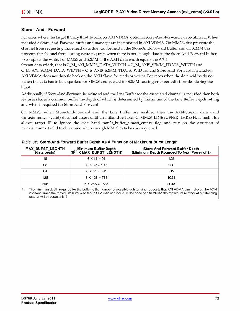
DS799 June 22, 2011 www.xilinx.com 72Product Specification
LogiCORE IP AXI Video Direct Memory Access (axi_vdma) (v3.01.a)
Store - And - Forward
For cases where the target IP may throttle back on AXI VDMA, optional Store-And-Forward can be utilized. When included a Store-And-Forward buffer and manager are instantiated in AXI VDMA. On MM2S, this prevents the channel from requesting more read data than can be held in the Store-And-Forward buffer and on S2MM this prevents the channel from issuing write requests when there is not enough data in the Store-And-Forward buffer to complete the write. For MM2S and S2MM, if the AXI4 data width equals the AXI4Stream data width, that is C_M_AXI_MM2S_DATA_WIDTH = C_M_AXIS_S2MM_TDATA_WIDTH andC_M_AXI_S2MM_DATA_WIDTH = C_S_AXIS_S2MM_TDATA_WIDTH, and Store-And-Forward is included, AXI VDMA does not throttle back on the AXI4 Slave for reads or writes. For cases when the data widths do not match the data has to be unpacked for MM2S and packed for S2MM causing brief periodic throttles during the burst.
Additionally if Store-And-Forward is included and the Line Buffer for the associated channel is included then bothfeatures shares a common buffer the depth of which is determined by maximum of the Line Buffer Depth settingand what is required for Store-And-Forward.
On MM2S, when Store-And-Forward and the Line Buffer are enabled then the AXI4-Stream data valid(m_axis_mm2s_tvalid) does not assert until an initial threshold, C_MM2S_LINEBUFFER_THRESH, is met. Thisallows target IP to ignore the side band mm2s_buffer_almost_empty flag and rely on the assertion ofm_axis_mm2s_tvalid to determine when enough MM2S data has been queued.
Table 36: Store-And-Forward Buffer Depth As A Function of Maximum Burst Length
MAX_BURST_LEGNTH (data beats)
Minimum Buffer Depth(6(1) X MAX_BURST_LENGTH)
Store-And-Forward Buffer Depth(Minimum Depth Rounded To Next Power of 2)
16 6 X 16 = 96 128
32 6 X 32 = 192 256
64 6 X 64 = 384 512
128 6 X 128 = 768 1024
256 6 X 256 = 1536 2048
1. The minimum depth required for the buffer is the number of possible outstanding requests that AXI VDMA can make on the AXI4 interface times the maximum burst size that AXI VDMA can issue. In the case of AXI VDMA the maximum number of outstanding read or write requests is 6.
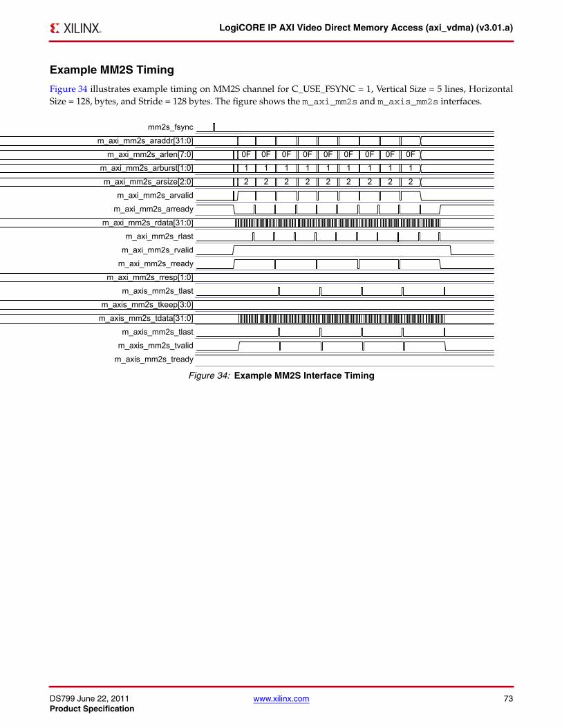
DS799 June 22, 2011 www.xilinx.com 73Product Specification
LogiCORE IP AXI Video Direct Memory Access (axi_vdma) (v3.01.a)
Example MM2S Timing
Figure 34 illustrates example timing on MM2S channel for C_USE_FSYNC = 1, Vertical Size = 5 lines, HorizontalSize = 128, bytes, and Stride = 128 bytes. The figure shows the m_axi_mm2s and m_axis_mm2s interfaces.X-Ref Target - Figure 34
Figure 34: Example MM2S Interface Timing
mm2s_fsync
m_axi_mm2s_araddr[31:0]
m_axi_mm2s_arlen[7:0]
m_axi_mm2s_arburst[1:0]
m_axi_mm2s_arsize[2:0]
m_axi_mm2s_arvalid
m_axi_mm2s_arready
m_axi_mm2s_rdata[31:0]
m_axi_mm2s_rlast
m_axi_mm2s_rvalid
m_axi_mm2s_rready
m_axi_mm2s_rresp[1:0]
m_axis_mm2s_tlast
m_axis_mm2s_tkeep[3:0]
m_axis_mm2s_tdata[31:0]
m_axis_mm2s_tlast
m_axis_mm2s_tvalid
m_axis_mm2s_tready
0F 0F 0F 0F 0F 0F 0F 0F 0F
1 1 1 1 1 1 1 1 1
2 2 2 2 2 2 2 2 2
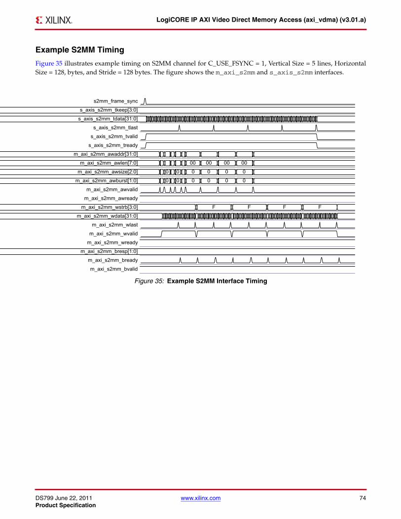
DS799 June 22, 2011 www.xilinx.com 74Product Specification
LogiCORE IP AXI Video Direct Memory Access (axi_vdma) (v3.01.a)
Example S2MM Timing
Figure 35 illustrates example timing on S2MM channel for C_USE_FSYNC = 1, Vertical Size = 5 lines, HorizontalSize = 128, bytes, and Stride = 128 bytes. The figure shows the m_axi_s2mm and s_axis_s2mm interfaces.
X-Ref Target - Figure 35
Figure 35: Example S2MM Interface Timing
s2mm_frame_sync
s_axis_s2mm_tkeep[3:0]
s_axis_s2mm_tdata[31:0]
s_axis_s2mm_tlast
s_axis_s2mm_tvalid
s_axis_s2mm_tready
m_axi_s2mm_awaddr[31:0]
m_axi_s2mm_awlen[7:0]
m_axi_s2mm_awsize[2:0]
m_axi_s2mm_awburst[1:0]
m_axi_s2mm_awvalid
m_axi_s2mm_awready
m_axi_s2mm_wstrb[3:0]
m_axi_s2mm_wdata[31:0]
m_axi_s2mm_wlast
m_axi_s2mm_wvalid
m_axi_s2mm_wready
m_axi_s2mm_bresp[1:0]
m_axi_s2mm_bready
m_axi_s2mm_bvalid
00 00 00 00
0 0 0 0 0 0
0 0 0 0 0 0
F F F F
DS799 June 22, 2011 www.xilinx.com 75Product Specification
LogiCORE IP AXI Video Direct Memory Access (axi_vdma) (v3.01.a)
Example Scatter Gather Timing
Figure 36 illustrates example timing for the Scatter Gather interface. The figure shows m_axi_sg interface timingwith respect to m_axi_mm2s interface.X-Ref Target - Figure 36
Figure 36: Example Scatter Gather Timing
mm2s_dmacr[31:0]mm2s_dmasr[31:0]
mm2s_curdesc[31:0]mm2s_taildesc[31:0]
m_axi_sg_araddr[31:0]m_axi_sg_arsize[2:0]m_axi_sg_arlen[7:0]
m_axi_sg_arburst[1:0]m_axi_sg_arvalid
m_axi_sg_arreadym_axi_sg_rdata[31:0]
m_axi_sg_rlastm_axi_sg_rresp[1:0]
m_axi_sg_rvalidm_axi_sg_rready
mm2s_fsyncm_axi_mm2s_araddr[31:0]m_axi_mm2s_arburst[1:0]
m_axi_mm2s_arlen[7:0]m_axi_mm2s_arsize[2:0]
m_axi_mm2s_arvalidm_axi_mm2s_arready
m_axi_mm2s_rdata[31:0]m_axi_mm2s_rlast
m_axi_mm2s_rresp[1:0]m_axi_mm2s_rready
m_axis_mm2s_tkeep[3:0]m_axis_mm2s_tdata[31:0]
m_axis_mm2s_tlastm_axis_mm2s_tvalid
m_axis_mm2s_tready
0001000200010001 00080000
30000000
00000000 30000100
000000000 0 0 0 0
00 00 00 00 000 0 0 0 0
00000000
00000000 500000800 1 100 0F 0F0 2 2
00000000
000000000
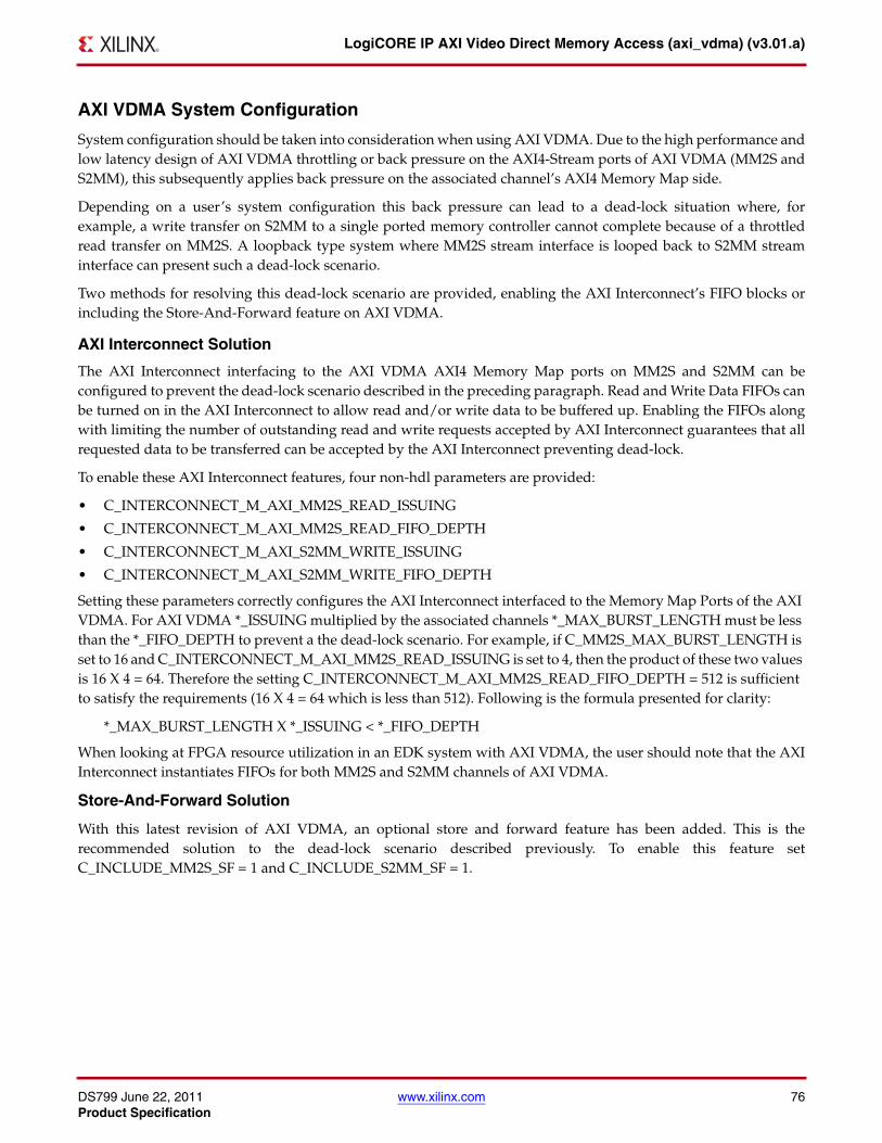
DS799 June 22, 2011 www.xilinx.com 76Product Specification
LogiCORE IP AXI Video Direct Memory Access (axi_vdma) (v3.01.a)
AXI VDMA System Configuration
System configuration should be taken into consideration when using AXI VDMA. Due to the high performance andlow latency design of AXI VDMA throttling or back pressure on the AXI4-Stream ports of AXI VDMA (MM2S andS2MM), this subsequently applies back pressure on the associated channel’s AXI4 Memory Map side.
Depending on a user’s system configuration this back pressure can lead to a dead-lock situation where, forexample, a write transfer on S2MM to a single ported memory controller cannot complete because of a throttledread transfer on MM2S. A loopback type system where MM2S stream interface is looped back to S2MM streaminterface can present such a dead-lock scenario.
Two methods for resolving this dead-lock scenario are provided, enabling the AXI Interconnect’s FIFO blocks orincluding the Store-And-Forward feature on AXI VDMA.
AXI Interconnect Solution
The AXI Interconnect interfacing to the AXI VDMA AXI4 Memory Map ports on MM2S and S2MM can beconfigured to prevent the dead-lock scenario described in the preceding paragraph. Read and Write Data FIFOs canbe turned on in the AXI Interconnect to allow read and/or write data to be buffered up. Enabling the FIFOs alongwith limiting the number of outstanding read and write requests accepted by AXI Interconnect guarantees that allrequested data to be transferred can be accepted by the AXI Interconnect preventing dead-lock.
To enable these AXI Interconnect features, four non-hdl parameters are provided:
• C_INTERCONNECT_M_AXI_MM2S_READ_ISSUING
• C_INTERCONNECT_M_AXI_MM2S_READ_FIFO_DEPTH
• C_INTERCONNECT_M_AXI_S2MM_WRITE_ISSUING
• C_INTERCONNECT_M_AXI_S2MM_WRITE_FIFO_DEPTH
Setting these parameters correctly configures the AXI Interconnect interfaced to the Memory Map Ports of the AXI VDMA. For AXI VDMA *_ISSUING multiplied by the associated channels *_MAX_BURST_LENGTH must be less than the *_FIFO_DEPTH to prevent a the dead-lock scenario. For example, if C_MM2S_MAX_BURST_LENGTH is set to 16 and C_INTERCONNECT_M_AXI_MM2S_READ_ISSUING is set to 4, then the product of these two values is 16 X 4 = 64. Therefore the setting C_INTERCONNECT_M_AXI_MM2S_READ_FIFO_DEPTH = 512 is sufficient to satisfy the requirements (16 X 4 = 64 which is less than 512). Following is the formula presented for clarity:
*_MAX_BURST_LENGTH X *_ISSUING < *_FIFO_DEPTH
When looking at FPGA resource utilization in an EDK system with AXI VDMA, the user should note that the AXIInterconnect instantiates FIFOs for both MM2S and S2MM channels of AXI VDMA.
Store-And-Forward Solution
With this latest revision of AXI VDMA, an optional store and forward feature has been added. This is therecommended solution to the dead-lock scenario described previously. To enable this feature setC_INCLUDE_MM2S_SF = 1 and C_INCLUDE_S2MM_SF = 1.
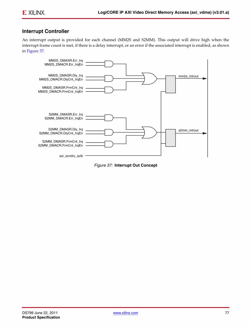
DS799 June 22, 2011 www.xilinx.com 77Product Specification
LogiCORE IP AXI Video Direct Memory Access (axi_vdma) (v3.01.a)
Interrupt Controller
An interrupt output is provided for each channel (MM2S and S2MM). This output will drive high when theinterrupt frame count is met, if there is a delay interrupt, or an error if the associated interrupt is enabled, as shownin Figure 37.X-Ref Target - Figure 37
Figure 37: Interrupt Out Concept
MM2S_DMASR.Err_IrqMM2S_DMACR.Err_IrqEn
MM2S_DMASR.Dly_IrqMM2S_DMACR.DlyCnt_IrqEn
MM2S_DMASR.FrmCnt_IrqMM2S_DMACR.FrmCnt_IrqEn
S2MM_DMASR.Err_IrqS2MM_DMACR.Err_IrqEn
S2MM_DMASR.Dly_IrqS2MM_DMACR.DlyCnt_IrqEn
S2MM_DMASR.FrmCnt_IrqS2MM_DMACR.FrmCnt_IrqEn
axi_scndry_aclk
mm2s_introut
s2mm_introut
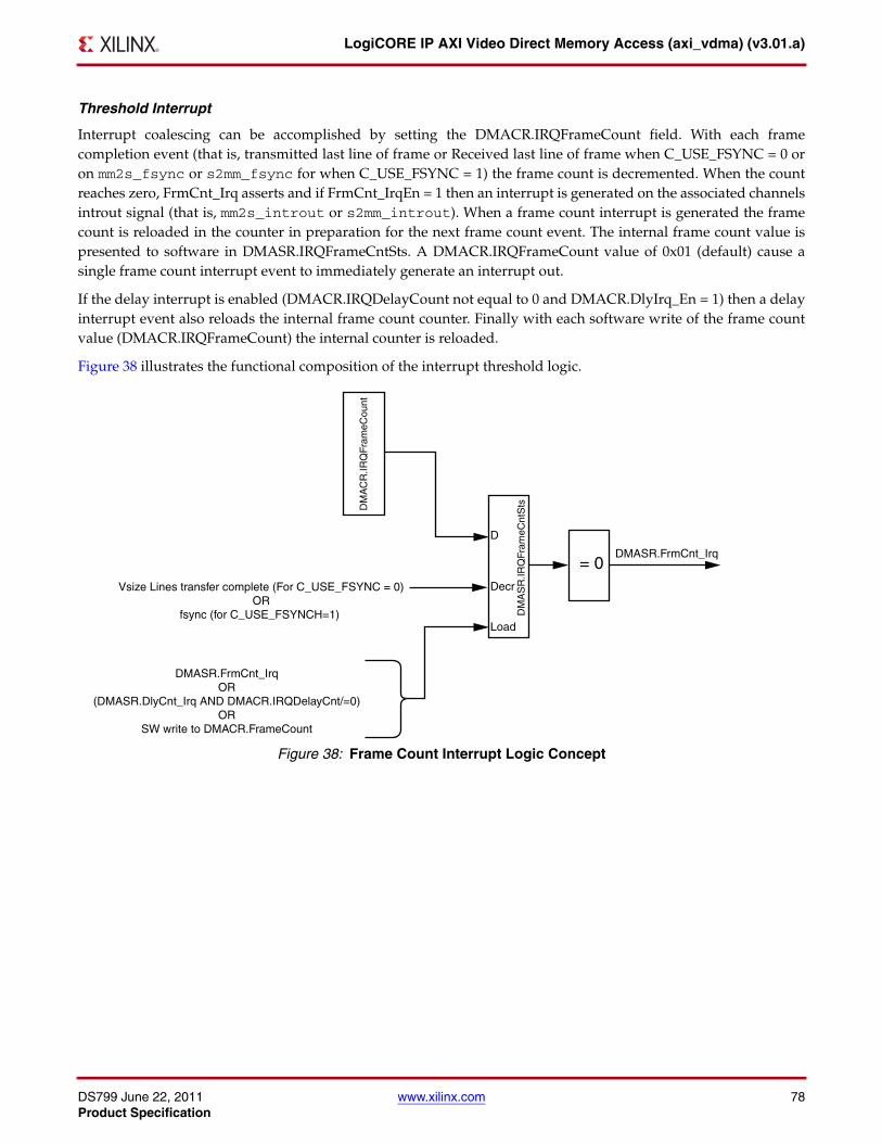
DS799 June 22, 2011 www.xilinx.com 78Product Specification
LogiCORE IP AXI Video Direct Memory Access (axi_vdma) (v3.01.a)
Threshold Interrupt
Interrupt coalescing can be accomplished by setting the DMACR.IRQFrameCount field. With each framecompletion event (that is, transmitted last line of frame or Received last line of frame when C_USE_FSYNC = 0 oron mm2s_fsync or s2mm_fsync for when C_USE_FSYNC = 1) the frame count is decremented. When the countreaches zero, FrmCnt_Irq asserts and if FrmCnt_IrqEn = 1 then an interrupt is generated on the associated channelsintrout signal (that is, mm2s_introut or s2mm_introut). When a frame count interrupt is generated the framecount is reloaded in the counter in preparation for the next frame count event. The internal frame count value ispresented to software in DMASR.IRQFrameCntSts. A DMACR.IRQFrameCount value of 0x01 (default) cause asingle frame count interrupt event to immediately generate an interrupt out.
If the delay interrupt is enabled (DMACR.IRQDelayCount not equal to 0 and DMACR.DlyIrq_En = 1) then a delayinterrupt event also reloads the internal frame count counter. Finally with each software write of the frame countvalue (DMACR.IRQFrameCount) the internal counter is reloaded.
Figure 38 illustrates the functional composition of the interrupt threshold logic.X-Ref Target - Figure 38
Figure 38: Frame Count Interrupt Logic Concept
Vsize Lines transfer complete (For C_USE_FSYNC = 0)OR
fsync (for C_USE_FSYNCH=1)
DMASR.FrmCnt_IrqOR
(DMASR.DlyCnt_Irq AND DMACR.IRQDelayCnt/=0)OR
SW write to DMACR.FrameCount
= 0DMASR.FrmCnt_Irq
D
Decr
Load
DM
AC
R.IR
QFr
ameC
ount
DM
AS
R.IR
QFr
ameC
ntS
ts
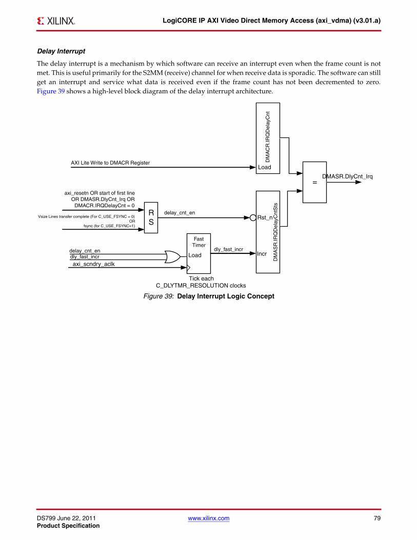
DS799 June 22, 2011 www.xilinx.com 79Product Specification
LogiCORE IP AXI Video Direct Memory Access (axi_vdma) (v3.01.a)
Delay Interrupt
The delay interrupt is a mechanism by which software can receive an interrupt even when the frame count is notmet. This is useful primarily for the S2MM (receive) channel for when receive data is sporadic. The software can stillget an interrupt and service what data is received even if the frame count has not been decremented to zero.Figure 39 shows a high-level block diagram of the delay interrupt architecture.X-Ref Target - Figure 39
Figure 39: Delay Interrupt Logic Concept
FastTimer
axi_scndry_aclk
Tick eachC_DLYTMR_RESOLUTION clocks
Incr
=
DM
AC
R.IR
QD
elay
Cnt
DMASR.DlyCnt_Irq
DM
AS
R.IR
QD
elay
Cnt
Sts
dly_fast_incrLoad
axi_resetn OR start of first line OR DMASR.DlyCnt_Irq OR
DMACR.IRQDelayCnt = 0
LoadAXI Lite Write to DMACR Register
Rst_nRS
delay_cnt_en
delay_cnt_endly_fast_incr
Vsize Lines transfer complete (For C_USE_FSYNC = 0)OR
fsync (for C_USE_FSYNC=1)
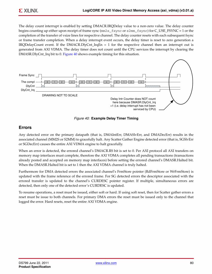
DS799 June 22, 2011 www.xilinx.com 80Product Specification
LogiCORE IP AXI Video Direct Memory Access (axi_vdma) (v3.01.a)
The delay count interrupt is enabled by setting DMACR.IRQDelay value to a non-zero value. The delay counterbegins counting up either upon receipt of frame sync (mm2s_fsync or s2mm_fsync) for C_USE_FSYNC = 1 or thecompletion of the transfer of vsize lines for respective channel. The delay counter resets with each subsequent fsyncor frame transfer completion. When a delay interrupt event occurs, the delay timer is reset to zero generation aIRQDelayCount event. If the DMACR.DlyCnt_IrqEn = 1 for the respective channel then an interrupt out isgenerated from AXI VDMA. The delay timer does not count until the CPU services the interrupt by clearing theDMASR.DlyCnt_Irq bit to 0. Figure 40 shows example timing for this situation.
Errors
Any detected error on the primary datapath (that is, DMAIntErr, DMASlvErr, and DMADecErr) results in theassociated channel (MM2S or S2MM) to gracefully halt. Any Scatter Gather Engine detected error (that is, SGSlvError SGDecErr) causes the entire AXI VDMA engine to halt gracefully.
When an error is detected, the errored channel’s DMACR.RS bit is set to 0. Per AXI protocol all AXI transfers onmemory map interfaces must complete, therefore the AXI VDMA completes all pending transactions (transactionsalready posted and accepted on memory map interfaces) before setting the errored channel’s DMASR.Halted bit.When the DMASR.Halted bit is set to 1 then the AXI VDMA channel is truly halted.
Furthermore for DMA detected errors the associated channel’s FrmStore pointer (RdFrmStore or WrFrmStore) isupdated with the frame reference of the errored frame. For SG detected errors the descriptor associated with theerrored transfer is updated to the channel’s CURDESC pointer register. If multiple, simultaneous errors aredetected, then only one of the detected error’s CURDESC is updated.
To resume operations, a reset must be issued, either soft or hard. If using soft reset, then for Scatter gather errors areset must be issue to both channels. For primary DMA errors the reset must be issued only to the channel thatlogged the error. Hard resets, reset the entire AXI VDMA engine.
X-Ref Target - Figure 40
Figure 40: Example Delay Timer Timing
Delay Intr Counter does NOT count here because DMASR.DlyCnt_Irq
=1 (i.e. delay interrupt has not been serviced by CPU)
DRAWING NOT TO SCALE
Frame Sync
The compl 0 1 2 n 0 1 2 n 0 1 2 n
DlyCntDlyCnt_Irq
DS799 June 22, 2011 www.xilinx.com 81Product Specification
LogiCORE IP AXI Video Direct Memory Access (axi_vdma) (v3.01.a)
Here is a list of possible errors:
DMAIntErr (C_INCLUDE_SG = 1/0)
DMA Internal Error flags an internal error in the AXI DataMover was detected. This can occur under twoconditions. First, for MM2S and S2MM channels, it can occur when a BTT = 0 is written to the primary AXIDataMover. For Scatter / Gather Mode (C_INCLUDE_SG = 1) this happens if a descriptor is fetched with the VSIZEor HSIZE = 0. For Register Direct Mode (C_INCLUDE_SG = 0) this happens if the VSIZE and/or HSIZE register forthe respective channel = 0 when the VSIZE register was written.
Secondly, for S2MM channels, the internal error can occur if an underflow or overflow condition occurs on theS2MM primary stream interface.
An underflow is defined as a condition where a received packet contains less bytes than what is specified by thehsize field.
An overflow is defined as a condition where a received packet contains more bytes than what is specified by thehsize field.
DMASlvErr (C_INCLUDE_SG = 1/0)
DMA Slave Error occurs when the slave to/from which data is transferred responds with a SLVERR on the memorymap interface.
DMADecErr (C_INCLUDE_SG = 1/0)
DMA Decode Error occurs when the address request is targeted to an address that does not exist.
SGSlvErr (C_INCLUDE_SG = 1)
Scatter Gather Slave Error occurs when the slave from which descriptors are fetched responds with a SLVERR.
SGDecErr (C_INCLUDE_SG = 1)
Scatter Gather Decode Error occurs when the address request is targeted to an address that does not exist.
DS799 June 22, 2011 www.xilinx.com 82Product Specification
LogiCORE IP AXI Video Direct Memory Access (axi_vdma) (v3.01.a)
Error Priority
Table 37 shows the error priorities and when the errors might occur.
Clock Domains
AXI VDMA provides two clocking modes of operation: asynchronous and synchronous. Asynchronous modeDMA control, Scatter Gather Engine, MM2S and S2MM Primary datapaths can all run asynchronously from eachother. Setting C_PRMRY_IS_ACLK_ASYNC = 1 enables this mode and creates four clock domains, AXI4-Lite clockdomain clocked by s_axi_lite_aclk, a Scatter / Gather clock domain clocked by m_axi_sg_aclk, and mm2sclock domain clocked by m_axi_mm2s_aclk, and s2mm clock domain clocked by m_axi_s2mm_aclk as shownin Figure 41. This allows high performance users to run the primary datapaths at a higher clock rates than the DMAcontrol (AXI4-Lite interface, SG Engine, DMA Controller, etc.) helping in FPGA placement and timing.
Table 37: Error Priority
Priority (1= highest
priority)Error Occurrence
1 Fetch SGSlvErr Cannot occur simultaneous with Fetch SGDecErr.
1 Fetch SGDecErr Cannot occur simultaneous with Fetch SGSlvErr.
2DMAIntErr
(that is, zero vsize or hsize error)
Cannot occur simultaneous with DMASlvErr or DMADecErr for the descriptor with the zero vsize or hsize error. Cannot occur simultaneously with Fetch SGDecErr, Fetch SGSlvErr, or Fetch SGIntErr for the descriptor with the zero vsize or hsize error.Can occur simultaneously with errors detected for other descriptors not having zero vsize or hsize error.
3DMAIntErr
(that is, Overflow/Underflow)
Cannot occur simultaneous with zero vsize or hsize error. Cannot occur simultaneously with Fetch SGDecErr, Fetch SGSlvErr, for the descriptor associated with overflow or underflow.Can occur simultaneous with DMASlvErr or DMADecErr.
3 DMADecErr Cannot occur simultaneous with DMASlvErr.
3 DMASlvErr Cannot occur simultaneous with DMADecErr.
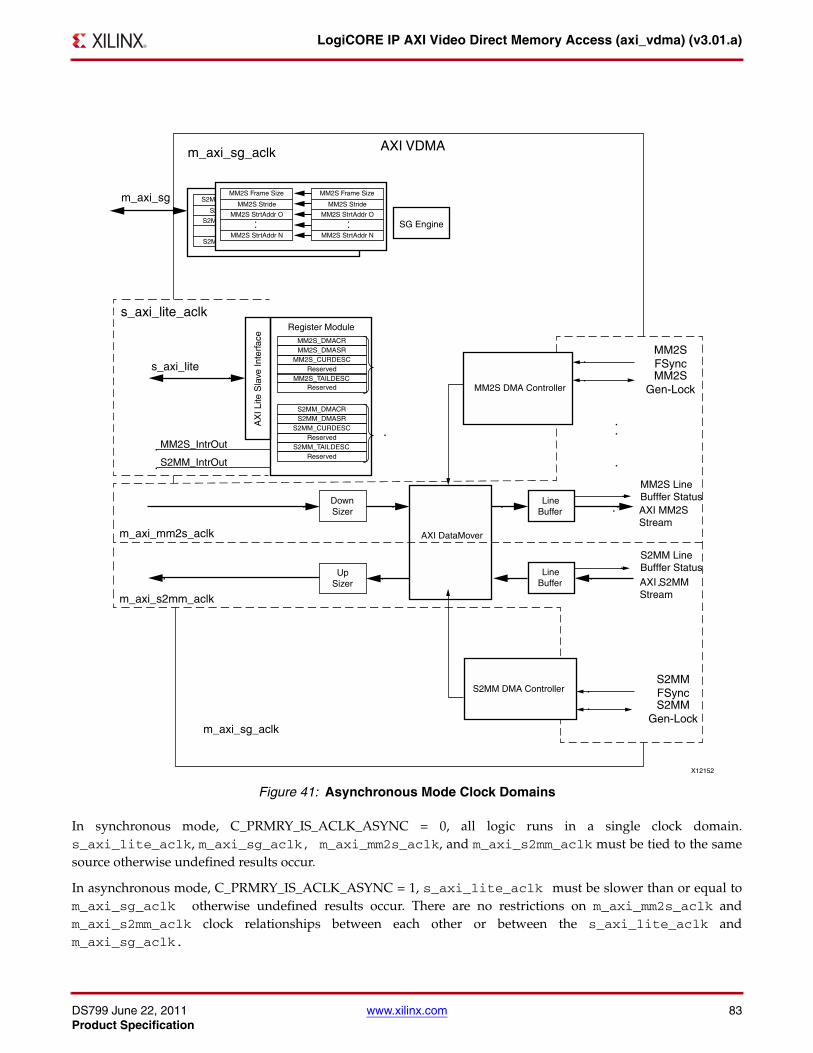
DS799 June 22, 2011 www.xilinx.com 83Product Specification
LogiCORE IP AXI Video Direct Memory Access (axi_vdma) (v3.01.a)
In synchronous mode, C_PRMRY_IS_ACLK_ASYNC = 0, all logic runs in a single clock domain.s_axi_lite_aclk, m_axi_sg_aclk, m_axi_mm2s_aclk, and m_axi_s2mm_aclk must be tied to the samesource otherwise undefined results occur.
In asynchronous mode, C_PRMRY_IS_ACLK_ASYNC = 1, s_axi_lite_aclk must be slower than or equal tom_axi_sg_aclk otherwise undefined results occur. There are no restrictions on m_axi_mm2s_aclk andm_axi_s2mm_aclk clock relationships between each other or between the s_axi_lite_aclk andm_axi_sg_aclk.
X-Ref Target - Figure 41
Figure 41: Asynchronous Mode Clock Domains
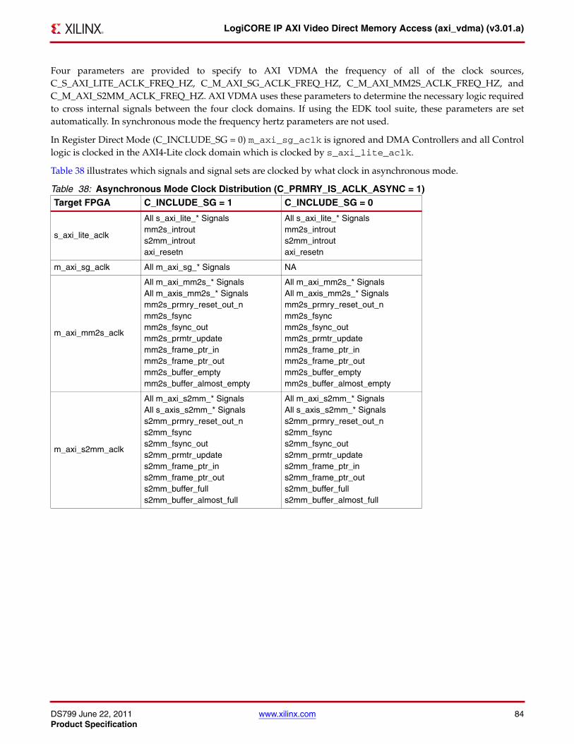
DS799 June 22, 2011 www.xilinx.com 84Product Specification
LogiCORE IP AXI Video Direct Memory Access (axi_vdma) (v3.01.a)
Four parameters are provided to specify to AXI VDMA the frequency of all of the clock sources,C_S_AXI_LITE_ACLK_FREQ_HZ, C_M_AXI_SG_ACLK_FREQ_HZ, C_M_AXI_MM2S_ACLK_FREQ_HZ, andC_M_AXI_S2MM_ACLK_FREQ_HZ. AXI VDMA uses these parameters to determine the necessary logic requiredto cross internal signals between the four clock domains. If using the EDK tool suite, these parameters are setautomatically. In synchronous mode the frequency hertz parameters are not used.
In Register Direct Mode (C_INCLUDE_SG = 0) m_axi_sg_aclk is ignored and DMA Controllers and all Controllogic is clocked in the AXI4-Lite clock domain which is clocked by s_axi_lite_aclk.
Table 38 illustrates which signals and signal sets are clocked by what clock in asynchronous mode.
Table 38: Asynchronous Mode Clock Distribution (C_PRMRY_IS_ACLK_ASYNC = 1)Target FPGA C_INCLUDE_SG = 1 C_INCLUDE_SG = 0
s_axi_lite_aclk
All s_axi_lite_* Signalsmm2s_introuts2mm_introutaxi_resetn
All s_axi_lite_* Signalsmm2s_introuts2mm_introutaxi_resetn
m_axi_sg_aclk All m_axi_sg_* Signals NA
m_axi_mm2s_aclk
All m_axi_mm2s_* SignalsAll m_axis_mm2s_* Signalsmm2s_prmry_reset_out_nmm2s_fsyncmm2s_fsync_outmm2s_prmtr_updatemm2s_frame_ptr_inmm2s_frame_ptr_outmm2s_buffer_emptymm2s_buffer_almost_empty
All m_axi_mm2s_* SignalsAll m_axis_mm2s_* Signalsmm2s_prmry_reset_out_nmm2s_fsyncmm2s_fsync_outmm2s_prmtr_updatemm2s_frame_ptr_inmm2s_frame_ptr_outmm2s_buffer_emptymm2s_buffer_almost_empty
m_axi_s2mm_aclk
All m_axi_s2mm_* SignalsAll s_axis_s2mm_* Signalss2mm_prmry_reset_out_ns2mm_fsyncs2mm_fsync_outs2mm_prmtr_updates2mm_frame_ptr_ins2mm_frame_ptr_outs2mm_buffer_fulls2mm_buffer_almost_full
All m_axi_s2mm_* SignalsAll s_axis_s2mm_* Signalss2mm_prmry_reset_out_ns2mm_fsyncs2mm_fsync_outs2mm_prmtr_updates2mm_frame_ptr_ins2mm_frame_ptr_outs2mm_buffer_fulls2mm_buffer_almost_full
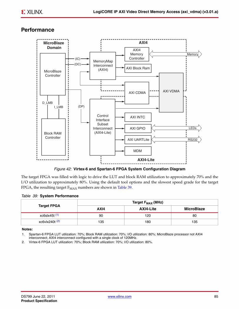
DS799 June 22, 2011 www.xilinx.com 85Product Specification
LogiCORE IP AXI Video Direct Memory Access (axi_vdma) (v3.01.a)
Performance
The target FPGA was filled with logic to drive the LUT and block RAM utilization to approximately 70% and theI/O utilization to approximately 80%. Using the default tool options and the slowest speed grade for the targetFPGA, the resulting target FMAX numbers are shown in Table 39.
X-Ref Target - Figure 42
Figure 42: Virtex-6 and Spartan-6 FPGA System Configuration Diagram
Table 39: System Performance
Target FPGATarget FMAX (MHz)
AXI4 AXI4-Lite MicroBlaze
xc6slx45t (1) 90 120 80
xc6vlx240t (2) 135 180 135
Notes: 1. Spartan-6 FPGA LUT utilization: 70%; Block RAM utilization: 70%; I/O utilization: 80%; MicroBlaze processor not AXI4
interconnect; AXI4 interconnect configured with a single clock of 120MHz.2. Virtex-6 FPGA LUT utilization: 70%; Block RAM utilization: 70%; I/O utilization: 80%.
AXI4-Lite
MicroBlazeController
AXI INTC
AXI GPIO
AXI UARTLite
AXI4Memory
Controller
MDM
MicroBlaze Domain
AXI4
Block RAMController
D_LMBI_LMB
(IC)
AXI Block Ram(DC)
AXI VDMA
Memory
(DP)
LEDs
RS232
AXI CDMA
MemoryMapInterconnect
(AXI4)
ControlInterfaceSubset
Interconnect(AXI4-Lite)
DS799 June 22, 2011 www.xilinx.com 86Product Specification
LogiCORE IP AXI Video Direct Memory Access (axi_vdma) (v3.01.a)
Latency and ThroughputTable 40 and Table 41 describes the latency and throughput for the AXI VDMA. The tables provides performanceinformation for a typical configuration. Throughput test consisted of 8 video frames for each channel with eachdescriptor describing a 1000 lines at 1000 bytes per line per frame (~1MByte) and each channel operatingsimultaneously (full duplex). Systems included a loopback module for looping MM2S channel data back to S2MMchannel data. Systems were configured for synchronous operation meaning s_axi_lite_aclk =
m_axi_sg_aclk = m_axi_mm2s_aclk = m_axi_s2mm_aclk. Throughput measured from completion ofdescriptor fetches (DMACR.Idle = 1) to frame count interrupt assertion. Latency measured in simulation andindicates AXI VDMA core latency cycles only and does not include system dependent latency or throttling.
System Configuration
• AXI VDMA Configuration
• C_USE_FSYNC = 0
• C_NUM_FSTORES = 8
• C_M_AXI_MM2S_DATA_WIDTH = 32 and C_M_AXI_S2MM_DATA_WIDTH = 32
• C_M_AXIS_MM2S_TDATA_WIDTH = 32 and C_S_AXIS_S2MM_TDATA_WIDTH = 32
• C_MM2S_MAX_BURST_LENGTH = 16 and C_S2MM_MAX_BURST_LENGTH = 16
• C_MM2S_GENLOCK_MODE = 0 and C_S2MM_GENLOCK_MODE = 0
• C_MM2S_LINEBUFFER_DEPTH = 0 and C_S2MM_LINEBUFFER_DEPTH = 0
• ML605 System
• Single Ported DDRx memory controller (Shared by CPU, AXI VDMA MM2S and S2MM, and AXI VDMA SG
• SP605 System
• Multiported DDRx memory controller (One port shared by AXI VDMA MM2S and S2MM, one port dedicated AXI VDMA SG, and one port dedicated to CPU)
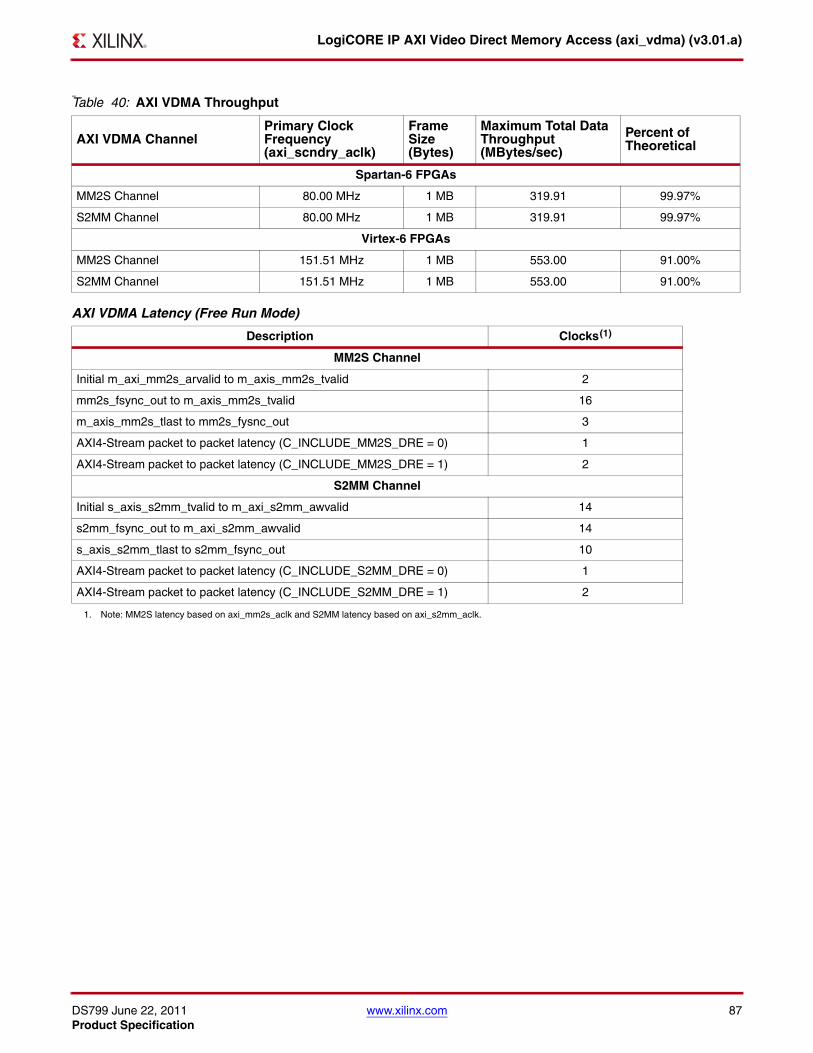
DS799 June 22, 2011 www.xilinx.com 87Product Specification
LogiCORE IP AXI Video Direct Memory Access (axi_vdma) (v3.01.a)
HH
Table 40: AXI VDMA Throughput
AXI VDMA ChannelPrimary Clock Frequency(axi_scndry_aclk)
Frame Size(Bytes)
Maximum Total Data Throughput(MBytes/sec)
Percent of Theoretical
Spartan-6 FPGAs
MM2S Channel 80.00 MHz 1 MB 319.91 99.97%
S2MM Channel 80.00 MHz 1 MB 319.91 99.97%
Virtex-6 FPGAs
MM2S Channel 151.51 MHz 1 MB 553.00 91.00%
S2MM Channel 151.51 MHz 1 MB 553.00 91.00%
AXI VDMA Latency (Free Run Mode)
Description Clocks(1)
1. Note: MM2S latency based on axi_mm2s_aclk and S2MM latency based on axi_s2mm_aclk.
MM2S Channel
Initial m_axi_mm2s_arvalid to m_axis_mm2s_tvalid 2
mm2s_fsync_out to m_axis_mm2s_tvalid 16
m_axis_mm2s_tlast to mm2s_fysnc_out 3
AXI4-Stream packet to packet latency (C_INCLUDE_MM2S_DRE = 0) 1
AXI4-Stream packet to packet latency (C_INCLUDE_MM2S_DRE = 1) 2
S2MM Channel
Initial s_axis_s2mm_tvalid to m_axi_s2mm_awvalid 14
s2mm_fsync_out to m_axi_s2mm_awvalid 14
s_axis_s2mm_tlast to s2mm_fsync_out 10
AXI4-Stream packet to packet latency (C_INCLUDE_S2MM_DRE = 0) 1
AXI4-Stream packet to packet latency (C_INCLUDE_S2MM_DRE = 1) 2
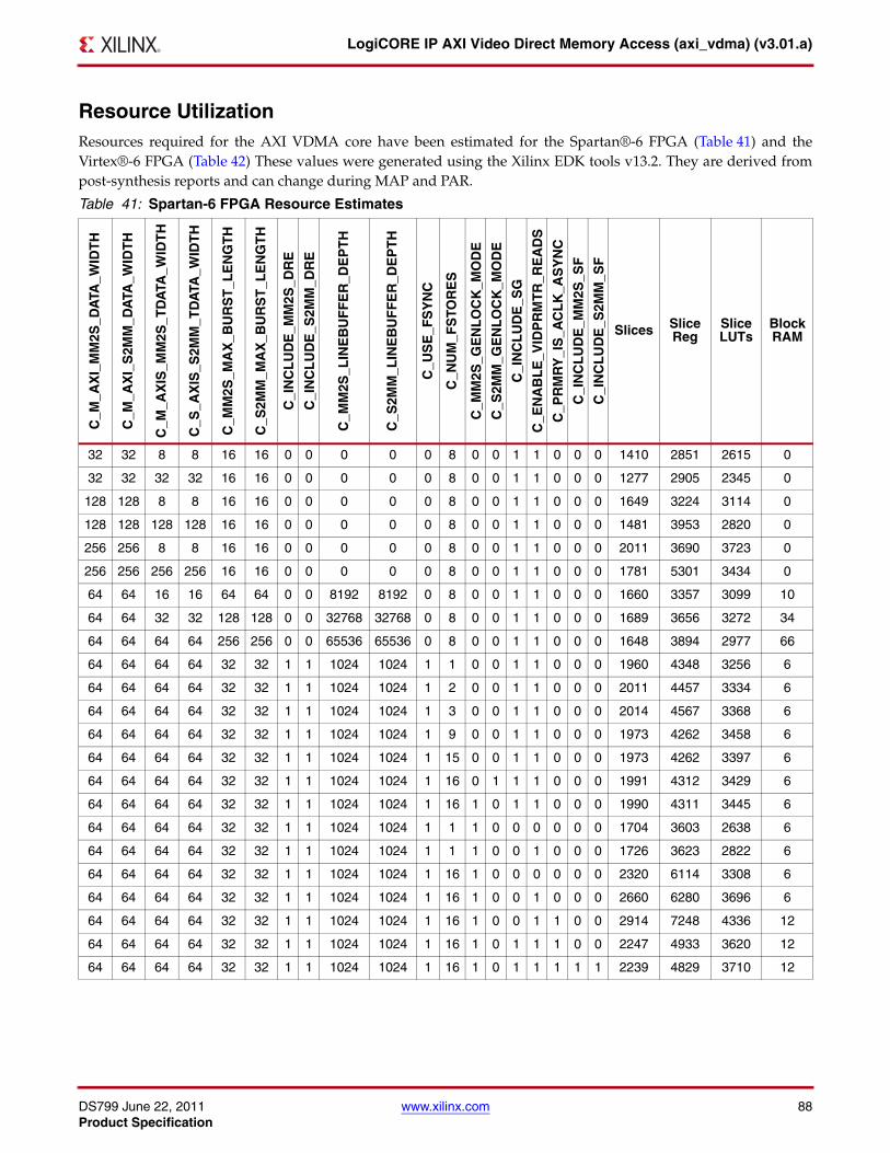
DS799 June 22, 2011 www.xilinx.com 88Product Specification
LogiCORE IP AXI Video Direct Memory Access (axi_vdma) (v3.01.a)
Resource UtilizationResources required for the AXI VDMA core have been estimated for the Spartan®-6 FPGA (Table 41) and theVirtex®-6 FPGA (Table 42) These values were generated using the Xilinx EDK tools v13.2. They are derived frompost-synthesis reports and can change during MAP and PAR.
Table 41: Spartan-6 FPGA Resource Estimates
C_M
_AX
I_M
M2S
_DA
TA_W
IDT
H
C_M
_AX
I_S
2MM
_DA
TA_W
IDT
H
C_M
_AX
IS_M
M2S
_TD
ATA
_WID
TH
C_S
_AX
IS_S
2MM
_TD
ATA
_WID
TH
C_M
M2S
_MA
X_B
UR
ST
_LE
NG
TH
C_S
2MM
_MA
X_B
UR
ST
_LE
NG
TH
C_I
NC
LU
DE
_MM
2S_D
RE
C_I
NC
LU
DE
_S2M
M_D
RE
C_M
M2S
_LIN
EB
UF
FE
R_D
EP
TH
C_S
2MM
_LIN
EB
UF
FE
R_D
EP
TH
C_U
SE
_FS
YN
C
C_N
UM
_FS
TOR
ES
C_M
M2S
_GE
NL
OC
K_M
OD
E
C_S
2MM
_GE
NL
OC
K_M
OD
E
C_I
NC
LU
DE
_SG
C_E
NA
BL
E_V
IDP
RM
TR
_RE
AD
S
C_P
RM
RY
_IS
_AC
LK
_AS
YN
C
C_I
NC
LU
DE
_MM
2S_S
F
C_I
NC
LU
DE
_S2M
M_S
F
Slices Slice Reg
Slice LUTs
Block RAM
32 32 8 8 16 16 0 0 0 0 0 8 0 0 1 1 0 0 0 1410 2851 2615 0
32 32 32 32 16 16 0 0 0 0 0 8 0 0 1 1 0 0 0 1277 2905 2345 0
128 128 8 8 16 16 0 0 0 0 0 8 0 0 1 1 0 0 0 1649 3224 3114 0
128 128 128 128 16 16 0 0 0 0 0 8 0 0 1 1 0 0 0 1481 3953 2820 0
256 256 8 8 16 16 0 0 0 0 0 8 0 0 1 1 0 0 0 2011 3690 3723 0
256 256 256 256 16 16 0 0 0 0 0 8 0 0 1 1 0 0 0 1781 5301 3434 0
64 64 16 16 64 64 0 0 8192 8192 0 8 0 0 1 1 0 0 0 1660 3357 3099 10
64 64 32 32 128 128 0 0 32768 32768 0 8 0 0 1 1 0 0 0 1689 3656 3272 34
64 64 64 64 256 256 0 0 65536 65536 0 8 0 0 1 1 0 0 0 1648 3894 2977 66
64 64 64 64 32 32 1 1 1024 1024 1 1 0 0 1 1 0 0 0 1960 4348 3256 6
64 64 64 64 32 32 1 1 1024 1024 1 2 0 0 1 1 0 0 0 2011 4457 3334 6
64 64 64 64 32 32 1 1 1024 1024 1 3 0 0 1 1 0 0 0 2014 4567 3368 6
64 64 64 64 32 32 1 1 1024 1024 1 9 0 0 1 1 0 0 0 1973 4262 3458 6
64 64 64 64 32 32 1 1 1024 1024 1 15 0 0 1 1 0 0 0 1973 4262 3397 6
64 64 64 64 32 32 1 1 1024 1024 1 16 0 1 1 1 0 0 0 1991 4312 3429 6
64 64 64 64 32 32 1 1 1024 1024 1 16 1 0 1 1 0 0 0 1990 4311 3445 6
64 64 64 64 32 32 1 1 1024 1024 1 1 1 0 0 0 0 0 0 1704 3603 2638 6
64 64 64 64 32 32 1 1 1024 1024 1 1 1 0 0 1 0 0 0 1726 3623 2822 6
64 64 64 64 32 32 1 1 1024 1024 1 16 1 0 0 0 0 0 0 2320 6114 3308 6
64 64 64 64 32 32 1 1 1024 1024 1 16 1 0 0 1 0 0 0 2660 6280 3696 6
64 64 64 64 32 32 1 1 1024 1024 1 16 1 0 0 1 1 0 0 2914 7248 4336 12
64 64 64 64 32 32 1 1 1024 1024 1 16 1 0 1 1 1 0 0 2247 4933 3620 12
64 64 64 64 32 32 1 1 1024 1024 1 16 1 0 1 1 1 1 1 2239 4829 3710 12
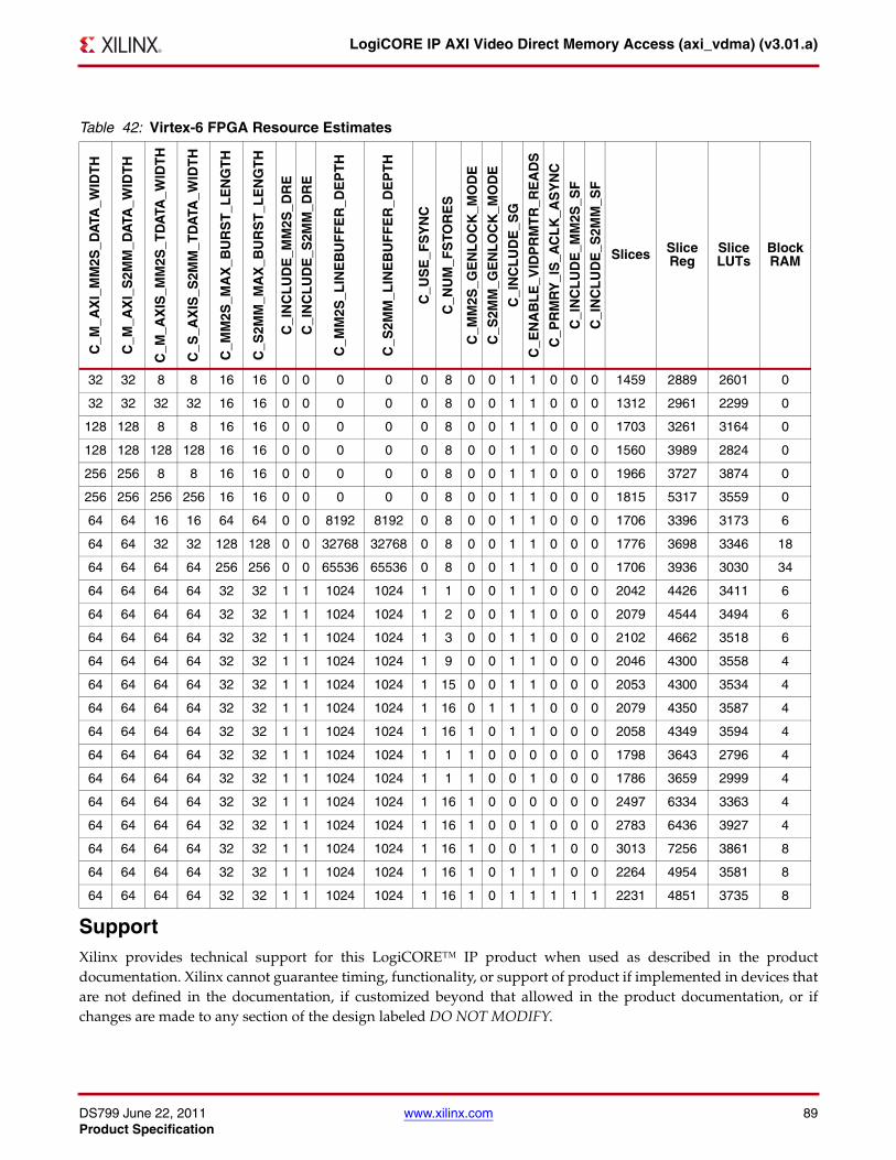
DS799 June 22, 2011 www.xilinx.com 89Product Specification
LogiCORE IP AXI Video Direct Memory Access (axi_vdma) (v3.01.a)
SupportXilinx provides technical support for this LogiCORE™ IP product when used as described in the productdocumentation. Xilinx cannot guarantee timing, functionality, or support of product if implemented in devices thatare not defined in the documentation, if customized beyond that allowed in the product documentation, or ifchanges are made to any section of the design labeled DO NOT MODIFY.
Table 42: Virtex-6 FPGA Resource Estimates
C_M
_AX
I_M
M2S
_DA
TA_W
IDT
H
C_M
_AX
I_S
2MM
_DA
TA_W
IDT
H
C_M
_AX
IS_M
M2S
_TD
ATA
_WID
TH
C_S
_AX
IS_S
2MM
_TD
ATA
_WID
TH
C_M
M2S
_MA
X_B
UR
ST
_LE
NG
TH
C_S
2MM
_MA
X_B
UR
ST
_LE
NG
TH
C_I
NC
LU
DE
_MM
2S_D
RE
C_I
NC
LU
DE
_S2M
M_D
RE
C_M
M2S
_LIN
EB
UF
FE
R_D
EP
TH
C_S
2MM
_LIN
EB
UF
FE
R_D
EP
TH
C_U
SE
_FS
YN
C
C_N
UM
_FS
TOR
ES
C_M
M2S
_GE
NL
OC
K_M
OD
E
C_S
2MM
_GE
NL
OC
K_M
OD
E
C_I
NC
LU
DE
_SG
C_E
NA
BL
E_V
IDP
RM
TR
_RE
AD
S
C_P
RM
RY
_IS
_AC
LK
_AS
YN
C
C_I
NC
LU
DE
_MM
2S_S
F
C_I
NC
LU
DE
_S2M
M_S
F
Slices Slice Reg
Slice LUTs
Block RAM
32 32 8 8 16 16 0 0 0 0 0 8 0 0 1 1 0 0 0 1459 2889 2601 0
32 32 32 32 16 16 0 0 0 0 0 8 0 0 1 1 0 0 0 1312 2961 2299 0
128 128 8 8 16 16 0 0 0 0 0 8 0 0 1 1 0 0 0 1703 3261 3164 0
128 128 128 128 16 16 0 0 0 0 0 8 0 0 1 1 0 0 0 1560 3989 2824 0
256 256 8 8 16 16 0 0 0 0 0 8 0 0 1 1 0 0 0 1966 3727 3874 0
256 256 256 256 16 16 0 0 0 0 0 8 0 0 1 1 0 0 0 1815 5317 3559 0
64 64 16 16 64 64 0 0 8192 8192 0 8 0 0 1 1 0 0 0 1706 3396 3173 6
64 64 32 32 128 128 0 0 32768 32768 0 8 0 0 1 1 0 0 0 1776 3698 3346 18
64 64 64 64 256 256 0 0 65536 65536 0 8 0 0 1 1 0 0 0 1706 3936 3030 34
64 64 64 64 32 32 1 1 1024 1024 1 1 0 0 1 1 0 0 0 2042 4426 3411 6
64 64 64 64 32 32 1 1 1024 1024 1 2 0 0 1 1 0 0 0 2079 4544 3494 6
64 64 64 64 32 32 1 1 1024 1024 1 3 0 0 1 1 0 0 0 2102 4662 3518 6
64 64 64 64 32 32 1 1 1024 1024 1 9 0 0 1 1 0 0 0 2046 4300 3558 4
64 64 64 64 32 32 1 1 1024 1024 1 15 0 0 1 1 0 0 0 2053 4300 3534 4
64 64 64 64 32 32 1 1 1024 1024 1 16 0 1 1 1 0 0 0 2079 4350 3587 4
64 64 64 64 32 32 1 1 1024 1024 1 16 1 0 1 1 0 0 0 2058 4349 3594 4
64 64 64 64 32 32 1 1 1024 1024 1 1 1 0 0 0 0 0 0 1798 3643 2796 4
64 64 64 64 32 32 1 1 1024 1024 1 1 1 0 0 1 0 0 0 1786 3659 2999 4
64 64 64 64 32 32 1 1 1024 1024 1 16 1 0 0 0 0 0 0 2497 6334 3363 4
64 64 64 64 32 32 1 1 1024 1024 1 16 1 0 0 1 0 0 0 2783 6436 3927 4
64 64 64 64 32 32 1 1 1024 1024 1 16 1 0 0 1 1 0 0 3013 7256 3861 8
64 64 64 64 32 32 1 1 1024 1024 1 16 1 0 1 1 1 0 0 2264 4954 3581 8
64 64 64 64 32 32 1 1 1024 1024 1 16 1 0 1 1 1 1 1 2231 4851 3735 8
DS799 June 22, 2011 www.xilinx.com 90Product Specification
LogiCORE IP AXI Video Direct Memory Access (axi_vdma) (v3.01.a)
Ordering InformationThis Xilinx LogiCORE IP module is provided at no additional cost with the Xilinx ISE® Design Suite EmbeddedEdition software under the terms of the Xilinx End User License. The core is generated using the Xilinx ISEEmbedded Edition software (EDK).
Information about this and other Xilinx LogiCORE IP modules is available at the Xilinx Intellectual Property page.For information on pricing and availability of other Xilinx LogiCORE IP modules and software, contact your localXilinx sales representative.
Reference DocumentationAXI Interconnect IP Data Sheet (DS768)
Go to www.xilinx.com/support/documentation/index.htm to search for Xilinx documentation.
List of AcronymsAcronym Spelled Out
AXI Advanced eXtensible Interface
CPU Central Processing Unit
DDR Double Data Rate
DMA Direct Memory Access
DRE Data Realignment Engine
DSP Digital Signal Processing
EDK Embedded Development Kit
FF Flip-Flop
FIFO First In First Out
FPGA Field Programmable Gate Array
IP Intellectual Property
ISE Integrated Software Environment
LUT Lookup Table
MM2S Memory Map to Stream
R/WC Read/Write to Clear
RAM Random Access Memory
RO Read Only
RW Read/Write
S2MM Stream to Memory Map
SG Scatter Gather
VDMA Video Direct Memory Access
XPS Xilinx Platform Studio (part of the EDK software)
XST Xilinx Synthesis Technology
DS799 June 22, 2011 www.xilinx.com 91Product Specification
LogiCORE IP AXI Video Direct Memory Access (axi_vdma) (v3.01.a)
Revision History
Notice of DisclaimerThe information disclosed to you hereunder (the “Materials”) is provided solely for the selection and use of Xilinx products. Tothe maximum extent permitted by applicable law: (1) Materials are made available “AS IS” and with all faults, Xilinx herebyDISCLAIMS ALL WARRANTIES AND CONDITIONS, EXPRESS, IMPLIED, OR STATUTORY, INCLUDING BUT NOTLIMITED TO WARRANTIES OF MERCHANTABILITY, NON-INFRINGEMENT, OR FITNESS FOR ANY PARTICULARPURPOSE; and (2) Xilinx shall not be liable (whether in contract or tort, including negligence, or under any other theory ofliability) for any loss or damage of any kind or nature related to, arising under, or in connection with, the Materials (includingyour use of the Materials), including for any direct, indirect, special, incidental, or consequential loss or damage (including lossof data, profits, goodwill, or any type of loss or damage suffered as a result of any action brought by a third party) even if suchdamage or loss was reasonably foreseeable or Xilinx had been advised of the possibility of the same. Xilinx assumes noobligation to correct any errors contained in the Materials or to notify you of updates to the Materials or to productspecifications. You may not reproduce, modify, distribute, or publicly display the Materials without prior written consent.Certain products are subject to the terms and conditions of the Limited Warranties which can be viewed athttp://www.xilinx.com/warranty.htm; IP cores may be subject to warranty and support terms contained in a license issued toyou by Xilinx. Xilinx products are not designed or intended to be fail-safe or for use in any application requiring fail-safeperformance; you assume sole risk and liability for use of Xilinx products in Critical Applications:http://www.xilinx.com/warranty.htm#critapps.
.
Date Version Description of Revisions
09/21/10 1.0 First release of the core with AXI interface support.
12/14/10 2.0 Updated for v2.00. a core version; updated for 12.4 tools.
03/01/11 3.0 Updated for v3.00. a core version; updated for 13.1 tools.
06/22/11 4.0 Updated for v3.01. a core version; updated for 13.2 tools.