Embed Size (px)
Citation preview
7 Series FPGAsClocking Resources
User Guide
UG472 (v1.14) July 30, 2018

7 Series FPGAs Clocking Resources User Guide www.xilinx.com UG472 (v1.14) July 30, 2018
The information disclosed to you hereunder (the “Materials”) is provided solely for the selection and use of Xilinx products. To the maximum extent permitted by applicable law: (1) Materials are made available "AS IS" and with all faults, Xilinx hereby DISCLAIMS ALL WARRANTIES AND CONDITIONS, EXPRESS, IMPLIED, OR STATUTORY, INCLUDING BUT NOT LIMITED TO WARRANTIES OF MERCHANTABILITY, NON-INFRINGEMENT, OR FITNESS FOR ANY PARTICULAR PURPOSE; and (2) Xilinx shall not be liable (whether in contract or tort, including negligence, or under any other theory of liability) for any loss or damage of any kind or nature related to, arising under, or in connection with, the Materials (including your use of the Materials), including for any direct, indirect, special, incidental, or consequential loss or damage (including loss of data, profits, goodwill, or any type of loss or damage suffered as a result of any action brought by a third party) even if such damage or loss was reasonably foreseeable or Xilinx had been advised of the possibility of the same. Xilinx assumes no obligation to correct any errors contained in the Materials or to notify you of updates to the Materials or to product specifications. You may not reproduce, modify, distribute, or publicly display the Materials without prior written consent. Certain products are subject to the terms and conditions of Xilinx’s limited warranty, please refer to Xilinx’s Terms of Sale which can be viewed at www.xilinx.com/legal.htm#tos; IP cores may be subject to warranty and support terms contained in a license issued to you by Xilinx. Xilinx products are not designed or intended to be fail-safe or for use in any application requiring fail-safe performance; you assume sole risk and liability for use of Xilinx products in such critical applications, please refer to Xilinx’s Terms of Sale which can be viewed at www.xilinx.com/legal.htm#tos.
Automotive Applications Disclaimer
AUTOMOTIVE PRODUCTS (IDENTIFIED AS "XA" IN THE PART NUMBER) ARE NOT WARRANTED FOR USE IN THE DEPLOYMENT OF AIRBAGS OR FOR USE IN APPLICATIONS THAT AFFECT CONTROL OF A VEHICLE ("SAFETY APPLICATION") UNLESS THERE IS A SAFETY CONCEPT OR REDUNDANCY FEATURE CONSISTENT WITH THE ISO 26262 AUTOMOTIVE SAFETY STANDARD ("SAFETY DESIGN"). CUSTOMER SHALL, PRIOR TO USING OR DISTRIBUTING ANY SYSTEMS THAT INCORPORATE PRODUCTS, THOROUGHLY TEST SUCH SYSTEMS FOR SAFETY PURPOSES. USE OF PRODUCTS IN A SAFETY APPLICATION WITHOUT A SAFETY DESIGN IS FULLY AT THE RISK OF CUSTOMER, SUBJECT ONLY TO APPLICABLE LAWS AND REGULATIONS GOVERNING LIMITATIONS ON PRODUCT LIABILITY.
© Copyright 2011–2018 Xilinx, Inc. Xilinx, the Xilinx logo, Artix, ISE, Kintex, Spartan, Virtex, Vivado, Zynq, and other designated brands included herein are trademarks of Xilinx in the United States and other countries. PCI, PCIe, and PCI Express are trademarks of PCI-SIG and used under license. All other trademarks are the property of their respective owners.
UG472 (v1.14) July 30, 2018 www.xilinx.com 7 Series FPGAs Clocking Resources User Guide
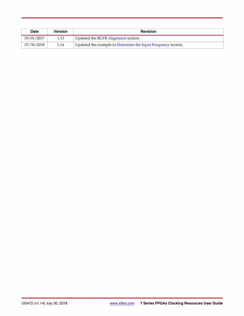
Revision HistoryThe following table shows the revision history for this document. .
Date Version Revision
03/01/2011 1.0 Initial Xilinx release.
03/28/2011 1.1 Updated disclaimer and copyright on page 2. Updated Clocking Architecture Overview and Figure 2-2. Revised the discussion in Clock-Capable Inputs including adding Table 1-1 and Figure 2-1. Revised some of the Global Clock Buffers descriptions. Revised the description under Figure 2-17. Updated the I/O Clock Buffer—BUFIO section. Updated Figure 2-20. Updated the Regional Clock Buffer—BUFR section. Updated the description in Table 2-8. Revised Figure 2-23. Added the BUFMRCE to the BUFMR Primitive section including Figure 2-25. Added BUFHCE to the Horizontal Clock Buffer—BUFH, BUFHCE section. Moved Clock Gating for Power Savings.
Updated the MMCMs and PLLs section. Revised the Frequency Synthesis Only Using Integer Divide section including Figure 3-4. Revised the discussion around adjacent regions in CLKOUT[0:6] – Output Clocks. Updated the examples after Equation 3-11. Moved and revised VHDL and Verilog Templates and the Clocking Wizard.
Added Appendix A, Multi-Region Clocking.
05/31/2011 1.2 Added section on 7 Series FPGAs Clocking Differences from Previous FPGA Generations.
Updated Figure 2-2. Clarified discussion in Clock-Capable Inputs section including removing Table 1-1: Migration of devices in the same package with different top/bottom alignments. Redrew Figure 2-4, Figure 2-16, Figure 2-18, and Figure 2-22.
Updated description of CLKOUT[0:6] in Table 3-5. Updated CLKFBSTOPPED – Feedback Clock Status, page 83. Clarified the MMCM/PLL relationship including updating Figure 3-10. Added more information to the Phase Shift section, including Equation 3-5.
Revised Figure A-6 and Figure A-7. Added Appendix B, Clocking Resources and Connectivity Variations per Clock Region.
10/27/2011 1.3 Moved 7 Series FPGAs Clocking Differences from Previous FPGA Generations. Added Clock Buffer Selection Considerations. Clarified description in Clock-Capable Inputs. Added another note after Figure 2-22, page 53. Added the Stacked Silicon Interconnect Clocking section.
Updated Figure 3-6, page 73. Clarified descriptions in Frequency Synthesis Using Fractional Divide in the MMCM, page 73, Interpolated Fine Phase Shift in Fixed or Dynamic Mode in the MMCM, page 75, Determine the Input Frequency, page 76, CLKOUT[0:6] – Output Clocks, page 82, and Reference Clock Switching, page 91. Revised description of STARTUP_WAIT, page 85. Updated RST description in Table 3-5, page 78. Updated CLKOUT[0]_DIVIDE_F(2) allowed values in Table 3-7, page 83. Updated Clock Network Deskew, page 72 adding Figure 3-12, page 92.
Updated Table B-1 and added Table B-2.
02/16/2012 1.4 Replaced “clocking backbone” with “clock backbone” and “clocking region” with “clock region” throughout.
Added Chapter 1, Clocking Overview, containing 7 Series FPGAs Clocking Differences from Previous FPGA Generations from Chapter 2 and Summary of Clock Connectivity from Appendix B. Updated Table 1-1. Removed XC7A8, XC7A15, XC7A30T, and XC7A50T from Table 1-2.
Added Clock-Capable Inputs. Updated Global Clocking Resources, including BUFMR Primitive. Updated Horizontal Clock Buffer—BUFH, BUFHCE. Updated paragraph before Figure 2-27.
7 Series FPGAs Clocking Resources User Guide www.xilinx.com UG472 (v1.14) July 30, 2018
02/16/2012 1.4(Cont’d)
In introductory paragraph of High-Performance Clocks, removed description of HPCs connecting to OSERDES and buffers. Replaced cross reference to UG429, 7 Series FPGAs Migration Methodology Guide, with UG872, Large FPGA Methodology Guide. Updated Stacked Silicon Interconnect Clocking. Replaced SRL with SLR in Figure 2-29. Added Figure 2-31.
Removed hold block from Figure 3-2. Updated clock frequencies in Frequency Synthesis Only Using Integer Divide. Replaced 64 with 63 in Equation 3-4. Updated Interpolated Fine Phase Shift in Fixed or Dynamic Mode in the MMCM. Updated pin description of LOCKED in Table 3-5. Updated LOCKED. In Table 3-7, updated type and allowed values of CLKOUT[0]_DIVIDE_F and CLKFBOUT_MULT_F, and description of STARTUP_WAIT and COMPENSATION. In Table 3-8, added STARTUP_WAIT and updated description of COMPENSATION. Replaced GTX with GT in Figure 3-10. Updated Dynamic Reconfiguration Port.
Added Appendix B, Clocking Resources and Connectivity Variations per Clock Region.
07/13/2012 1.5 Updated paragraph after Figure 1-4. Added bullet about spread spectrum support to Key Differences from Virtex-6 FPGAs. Updated BUFG and BUFH pins, and removed IBUFDS_GTE2.O/IBUFDS_GTE2.ODIV2 pin from Table 1-1. Updated Table 1-2.
Updated note 5 in Table 2-1. Added Figure 2-29.
Updated last sentence of Introduction. Updated DO[15:0] – Dynamic Reconfiguration Output Bus. Added SS_EN, SS_MODE, and SS_MOD_PERIOD to Table 3-7. Added Spread-Spectrum Clock Generation.
10/02/2012 1.6 Added note to Table 1-1. Removed XC7A350T and XC7V1500T from Table 1-2.
Updated first paragraph of Single Clock Driving Multiple CMTs. Added notes 5 and 8 to Table 2-1. Updated paragraph after Table 2-10.
Added Table 3-9 and timing constraint calculations for 25 MHz and 80 MHz input clocks. In Table 3-10, changed Bandwidth value from N/A to Low, and removed duplicate paragraph after table.
Removed XC7A350T from title of Figure B-4.
04/03/2013 1.7 Updated Figure 1-3, Figure B-2, and Figure B-3. Added BUFMR to Table 1-1. Updated second paragraph in Dynamic Phase Shift Interface in the MMCM. Added note to Table 2-7.
08/07/2013 1.8 Updated Table 1-2 and Table 3-7. Updated the figure titles for Figure B-2 and Figure B-3. Updated Clock Buffer Placement.
04/08/2014 1.9 Updated Clock-Capable Inputs and Dynamic Phase Shift Interface in the MMCM. Updated allowed values and the default value for CLKFBOUT_MULT in Table 3-8.
05/24/2014 1.10 Changed the value of minimum clock regions from six to four in Clocking Architecture Overview. Added information to MGTREFCLK0 in Table 1-1. Added section on GTZ Loopback Clock Buffer — BUFG_LB (HT devices only) to Chapter 2. Changed description of REF_JITTER1 and REF_JITTER2 in Table 3-7 and Table 3-8. Updated first paragraph in Use Cases.
11/19/2014 1.11 Removed general interconnect from this bulleted list on page 49. Updated the figure titles for Figure B-2 and Figure B-3.
03/04/2015 1.11.1 Updated Frequency Synthesis Using Fractional Divide in the MMCM, page 73 by changing 0.125 degrees to 0.125.
06/12/2015 1.11.2 Fixed broken link in three references to 7 Series FPGA Data Sheets on page 73 and page 74.
09/27/2016 1.12 Added the Spartan-7 FPGAs and the Artix-7 (XC7A12T and XC7A25T) devices where applicable including updating Appendix B. Updated the BUFR Alignment section. Updated the Automotive Applications Disclaimer.
Date Version Revision
UG472 (v1.14) July 30, 2018 www.xilinx.com 7 Series FPGAs Clocking Resources User Guide
03/01/2017 1.13 Updated the BUFR Alignment section.
07/30/2018 1.14 Updated the example in Determine the Input Frequency section.
Date Version Revision

7 Series FPGAs Clocking Resources User Guide www.xilinx.com UG472 (v1.14) July 30, 2018
7 Series FPGAs Clocking Resources User Guide www.xilinx.com 7UG472 (v1.14) July 30, 2018
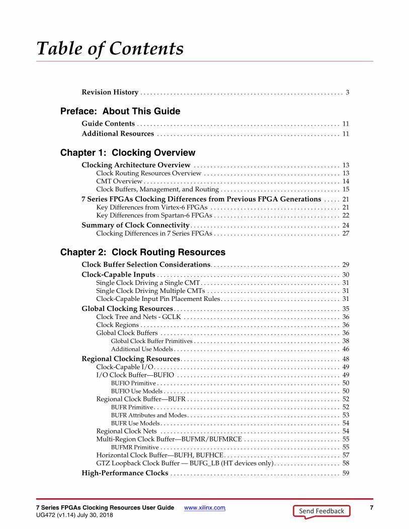
Revision History . . . . . . . . . . . . . . . . . . . . . . . . . . . . . . . . . . . . . . . . . . . . . . . . . . . . . . . . . . . . . 3
Preface: About This GuideGuide Contents . . . . . . . . . . . . . . . . . . . . . . . . . . . . . . . . . . . . . . . . . . . . . . . . . . . . . . . . . . . . . 11Additional Resources . . . . . . . . . . . . . . . . . . . . . . . . . . . . . . . . . . . . . . . . . . . . . . . . . . . . . . . 11
Chapter 1: Clocking OverviewClocking Architecture Overview . . . . . . . . . . . . . . . . . . . . . . . . . . . . . . . . . . . . . . . . . . . . 13
Clock Routing Resources Overview . . . . . . . . . . . . . . . . . . . . . . . . . . . . . . . . . . . . . . . . . 13CMT Overview . . . . . . . . . . . . . . . . . . . . . . . . . . . . . . . . . . . . . . . . . . . . . . . . . . . . . . . . . . . 14Clock Buffers, Management, and Routing . . . . . . . . . . . . . . . . . . . . . . . . . . . . . . . . . . . . 15
7 Series FPGAs Clocking Differences from Previous FPGA Generations . . . . . 21Key Differences from Virtex-6 FPGAs . . . . . . . . . . . . . . . . . . . . . . . . . . . . . . . . . . . . . . . 21Key Differences from Spartan-6 FPGAs . . . . . . . . . . . . . . . . . . . . . . . . . . . . . . . . . . . . . . 22
Summary of Clock Connectivity . . . . . . . . . . . . . . . . . . . . . . . . . . . . . . . . . . . . . . . . . . . . . 24Clocking Differences in 7 Series FPGAs . . . . . . . . . . . . . . . . . . . . . . . . . . . . . . . . . . . . . . 27
Chapter 2: Clock Routing ResourcesClock Buffer Selection Considerations. . . . . . . . . . . . . . . . . . . . . . . . . . . . . . . . . . . . . . . 29Clock-Capable Inputs . . . . . . . . . . . . . . . . . . . . . . . . . . . . . . . . . . . . . . . . . . . . . . . . . . . . . . . 30
Single Clock Driving a Single CMT . . . . . . . . . . . . . . . . . . . . . . . . . . . . . . . . . . . . . . . . . . 31Single Clock Driving Multiple CMTs . . . . . . . . . . . . . . . . . . . . . . . . . . . . . . . . . . . . . . . . 31Clock-Capable Input Pin Placement Rules . . . . . . . . . . . . . . . . . . . . . . . . . . . . . . . . . . . . 31
Global Clocking Resources . . . . . . . . . . . . . . . . . . . . . . . . . . . . . . . . . . . . . . . . . . . . . . . . . . 35Clock Tree and Nets - GCLK . . . . . . . . . . . . . . . . . . . . . . . . . . . . . . . . . . . . . . . . . . . . . . . 36Clock Regions . . . . . . . . . . . . . . . . . . . . . . . . . . . . . . . . . . . . . . . . . . . . . . . . . . . . . . . . . . . . 36Global Clock Buffers . . . . . . . . . . . . . . . . . . . . . . . . . . . . . . . . . . . . . . . . . . . . . . . . . . . . . . 36
Global Clock Buffer Primitives . . . . . . . . . . . . . . . . . . . . . . . . . . . . . . . . . . . . . . . . . . . . 38Additional Use Models . . . . . . . . . . . . . . . . . . . . . . . . . . . . . . . . . . . . . . . . . . . . . . . . . . 46
Regional Clocking Resources . . . . . . . . . . . . . . . . . . . . . . . . . . . . . . . . . . . . . . . . . . . . . . . . 48Clock-Capable I/O. . . . . . . . . . . . . . . . . . . . . . . . . . . . . . . . . . . . . . . . . . . . . . . . . . . . . . . . 49I/O Clock Buffer—BUFIO . . . . . . . . . . . . . . . . . . . . . . . . . . . . . . . . . . . . . . . . . . . . . . . . . 49
BUFIO Primitive . . . . . . . . . . . . . . . . . . . . . . . . . . . . . . . . . . . . . . . . . . . . . . . . . . . . . . . 50BUFIO Use Models . . . . . . . . . . . . . . . . . . . . . . . . . . . . . . . . . . . . . . . . . . . . . . . . . . . . . 50
Regional Clock Buffer—BUFR . . . . . . . . . . . . . . . . . . . . . . . . . . . . . . . . . . . . . . . . . . . . . . 52BUFR Primitive . . . . . . . . . . . . . . . . . . . . . . . . . . . . . . . . . . . . . . . . . . . . . . . . . . . . . . . . 52BUFR Attributes and Modes. . . . . . . . . . . . . . . . . . . . . . . . . . . . . . . . . . . . . . . . . . . . . . 53BUFR Use Models . . . . . . . . . . . . . . . . . . . . . . . . . . . . . . . . . . . . . . . . . . . . . . . . . . . . . . 54
Regional Clock Nets . . . . . . . . . . . . . . . . . . . . . . . . . . . . . . . . . . . . . . . . . . . . . . . . . . . . . . 54Multi-Region Clock Buffer—BUFMR/BUFMRCE . . . . . . . . . . . . . . . . . . . . . . . . . . . . . 55
BUFMR Primitive . . . . . . . . . . . . . . . . . . . . . . . . . . . . . . . . . . . . . . . . . . . . . . . . . . . . . . 55Horizontal Clock Buffer—BUFH, BUFHCE. . . . . . . . . . . . . . . . . . . . . . . . . . . . . . . . . . . 57GTZ Loopback Clock Buffer — BUFG_LB (HT devices only). . . . . . . . . . . . . . . . . . . . 58
High-Performance Clocks . . . . . . . . . . . . . . . . . . . . . . . . . . . . . . . . . . . . . . . . . . . . . . . . . . . 59
Table of Contents
Send Feedback
8 www.xilinx.com 7 Series FPGAs Clocking Resources User GuideUG472 (v1.14) July 30, 2018
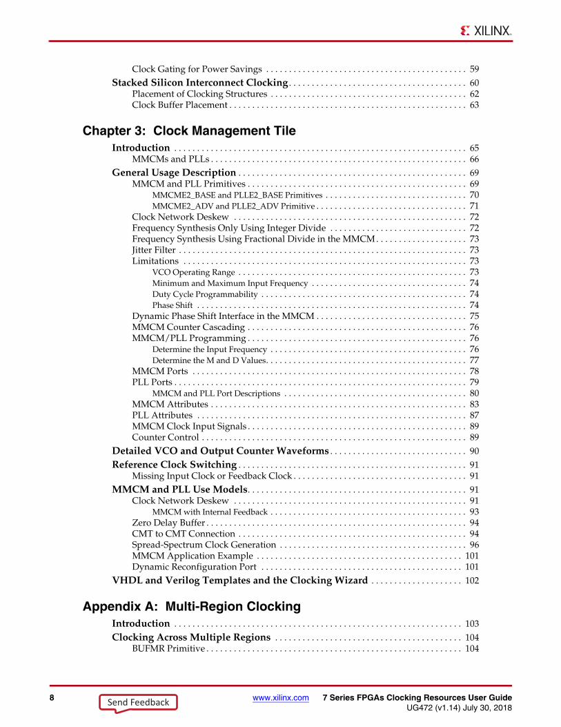
Clock Gating for Power Savings . . . . . . . . . . . . . . . . . . . . . . . . . . . . . . . . . . . . . . . . . . . . 59Stacked Silicon Interconnect Clocking . . . . . . . . . . . . . . . . . . . . . . . . . . . . . . . . . . . . . . . 60
Placement of Clocking Structures . . . . . . . . . . . . . . . . . . . . . . . . . . . . . . . . . . . . . . . . . . . 62Clock Buffer Placement . . . . . . . . . . . . . . . . . . . . . . . . . . . . . . . . . . . . . . . . . . . . . . . . . . . . 63
Chapter 3: Clock Management TileIntroduction . . . . . . . . . . . . . . . . . . . . . . . . . . . . . . . . . . . . . . . . . . . . . . . . . . . . . . . . . . . . . . . . 65
MMCMs and PLLs . . . . . . . . . . . . . . . . . . . . . . . . . . . . . . . . . . . . . . . . . . . . . . . . . . . . . . . . 66General Usage Description . . . . . . . . . . . . . . . . . . . . . . . . . . . . . . . . . . . . . . . . . . . . . . . . . . 69
MMCM and PLL Primitives . . . . . . . . . . . . . . . . . . . . . . . . . . . . . . . . . . . . . . . . . . . . . . . . 69MMCME2_BASE and PLLE2_BASE Primitives . . . . . . . . . . . . . . . . . . . . . . . . . . . . . . . 70MMCME2_ADV and PLLE2_ADV Primitive . . . . . . . . . . . . . . . . . . . . . . . . . . . . . . . . . 71
Clock Network Deskew . . . . . . . . . . . . . . . . . . . . . . . . . . . . . . . . . . . . . . . . . . . . . . . . . . . 72Frequency Synthesis Only Using Integer Divide . . . . . . . . . . . . . . . . . . . . . . . . . . . . . . 72Frequency Synthesis Using Fractional Divide in the MMCM. . . . . . . . . . . . . . . . . . . . 73Jitter Filter . . . . . . . . . . . . . . . . . . . . . . . . . . . . . . . . . . . . . . . . . . . . . . . . . . . . . . . . . . . . . . . 73Limitations . . . . . . . . . . . . . . . . . . . . . . . . . . . . . . . . . . . . . . . . . . . . . . . . . . . . . . . . . . . . . . 73
VCO Operating Range . . . . . . . . . . . . . . . . . . . . . . . . . . . . . . . . . . . . . . . . . . . . . . . . . . 73Minimum and Maximum Input Frequency . . . . . . . . . . . . . . . . . . . . . . . . . . . . . . . . . . 74Duty Cycle Programmability . . . . . . . . . . . . . . . . . . . . . . . . . . . . . . . . . . . . . . . . . . . . . 74Phase Shift . . . . . . . . . . . . . . . . . . . . . . . . . . . . . . . . . . . . . . . . . . . . . . . . . . . . . . . . . . . 74
Dynamic Phase Shift Interface in the MMCM . . . . . . . . . . . . . . . . . . . . . . . . . . . . . . . . . 75MMCM Counter Cascading . . . . . . . . . . . . . . . . . . . . . . . . . . . . . . . . . . . . . . . . . . . . . . . . 76MMCM/PLL Programming . . . . . . . . . . . . . . . . . . . . . . . . . . . . . . . . . . . . . . . . . . . . . . . . 76
Determine the Input Frequency . . . . . . . . . . . . . . . . . . . . . . . . . . . . . . . . . . . . . . . . . . . 76Determine the M and D Values. . . . . . . . . . . . . . . . . . . . . . . . . . . . . . . . . . . . . . . . . . . . 77
MMCM Ports . . . . . . . . . . . . . . . . . . . . . . . . . . . . . . . . . . . . . . . . . . . . . . . . . . . . . . . . . . . . 78PLL Ports . . . . . . . . . . . . . . . . . . . . . . . . . . . . . . . . . . . . . . . . . . . . . . . . . . . . . . . . . . . . . . . . 79
MMCM and PLL Port Descriptions . . . . . . . . . . . . . . . . . . . . . . . . . . . . . . . . . . . . . . . . 80MMCM Attributes . . . . . . . . . . . . . . . . . . . . . . . . . . . . . . . . . . . . . . . . . . . . . . . . . . . . . . . . 83PLL Attributes . . . . . . . . . . . . . . . . . . . . . . . . . . . . . . . . . . . . . . . . . . . . . . . . . . . . . . . . . . . 87MMCM Clock Input Signals . . . . . . . . . . . . . . . . . . . . . . . . . . . . . . . . . . . . . . . . . . . . . . . . 89Counter Control . . . . . . . . . . . . . . . . . . . . . . . . . . . . . . . . . . . . . . . . . . . . . . . . . . . . . . . . . . 89
Detailed VCO and Output Counter Waveforms . . . . . . . . . . . . . . . . . . . . . . . . . . . . . . 90Reference Clock Switching . . . . . . . . . . . . . . . . . . . . . . . . . . . . . . . . . . . . . . . . . . . . . . . . . . 91
Missing Input Clock or Feedback Clock . . . . . . . . . . . . . . . . . . . . . . . . . . . . . . . . . . . . . . 91MMCM and PLL Use Models. . . . . . . . . . . . . . . . . . . . . . . . . . . . . . . . . . . . . . . . . . . . . . . . 91
Clock Network Deskew . . . . . . . . . . . . . . . . . . . . . . . . . . . . . . . . . . . . . . . . . . . . . . . . . . . 91MMCM with Internal Feedback . . . . . . . . . . . . . . . . . . . . . . . . . . . . . . . . . . . . . . . . . . . 93
Zero Delay Buffer . . . . . . . . . . . . . . . . . . . . . . . . . . . . . . . . . . . . . . . . . . . . . . . . . . . . . . . . . 94CMT to CMT Connection . . . . . . . . . . . . . . . . . . . . . . . . . . . . . . . . . . . . . . . . . . . . . . . . . . 94Spread-Spectrum Clock Generation . . . . . . . . . . . . . . . . . . . . . . . . . . . . . . . . . . . . . . . . . 96MMCM Application Example . . . . . . . . . . . . . . . . . . . . . . . . . . . . . . . . . . . . . . . . . . . . . 101Dynamic Reconfiguration Port . . . . . . . . . . . . . . . . . . . . . . . . . . . . . . . . . . . . . . . . . . . . 101
VHDL and Verilog Templates and the Clocking Wizard . . . . . . . . . . . . . . . . . . . . 102
Appendix A: Multi-Region ClockingIntroduction . . . . . . . . . . . . . . . . . . . . . . . . . . . . . . . . . . . . . . . . . . . . . . . . . . . . . . . . . . . . . . . 103Clocking Across Multiple Regions . . . . . . . . . . . . . . . . . . . . . . . . . . . . . . . . . . . . . . . . . 104
BUFMR Primitive . . . . . . . . . . . . . . . . . . . . . . . . . . . . . . . . . . . . . . . . . . . . . . . . . . . . . . . . 104
Send Feedback
7 Series FPGAs Clocking Resources User Guide www.xilinx.com 9UG472 (v1.14) July 30, 2018
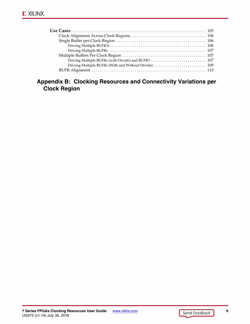
Use Cases . . . . . . . . . . . . . . . . . . . . . . . . . . . . . . . . . . . . . . . . . . . . . . . . . . . . . . . . . . . . . . . . . . 105Clock Alignment Across Clock Regions . . . . . . . . . . . . . . . . . . . . . . . . . . . . . . . . . . . . . 106Single Buffer per Clock Region . . . . . . . . . . . . . . . . . . . . . . . . . . . . . . . . . . . . . . . . . . . . 106
Driving Multiple BUFIOs . . . . . . . . . . . . . . . . . . . . . . . . . . . . . . . . . . . . . . . . . . . . . . . 106Driving Multiple BUFRs . . . . . . . . . . . . . . . . . . . . . . . . . . . . . . . . . . . . . . . . . . . . . . . . 107
Multiple Buffers Per Clock Region . . . . . . . . . . . . . . . . . . . . . . . . . . . . . . . . . . . . . . . . . 107Driving Multiple BUFRs (with Divide) and BUFIO . . . . . . . . . . . . . . . . . . . . . . . . . . . 107Driving Multiple BUFRs (With and Without Divide) . . . . . . . . . . . . . . . . . . . . . . . . . . 109
BUFR Alignment . . . . . . . . . . . . . . . . . . . . . . . . . . . . . . . . . . . . . . . . . . . . . . . . . . . . . . . . 110
Appendix B: Clocking Resources and Connectivity Variations per Clock Region
Send Feedback

10 www.xilinx.com 7 Series FPGAs Clocking Resources User GuideUG472 (v1.14) July 30, 2018
Send Feedback
7 Series FPGAs Clocking Resources User Guide www.xilinx.com 11UG472 (v1.14) July 30, 2018
Preface
About This Guide
Xilinx® 7 series FPGAs include four FPGA families that are all designed for lowest power to enable a common design to scale across families for optimal power, performance, and cost. The Spartan®-7 family is the lowest density with the lowest cost entry point into the 7 series portfolio. The Artix®-7 family is optimized for highest performance-per-watt and bandwidth-per-watt for cost-sensitive, high-volume applications. The Kintex®-7 family is an innovative class of FPGAs optimized for the best price-performance. The Virtex®-7 family is optimized for highest system performance and capacity.
This 7 series FPGAs clocking resources user guide, part of an overall set of documentation on the 7 series FPGAs, is available on the Xilinx website atwww.xilinx.com/documentation.
Guide ContentsThis manual contains the following chapters:
• Chapter 1, Clocking Overview
• Chapter 2, Clock Routing Resources
• Chapter 3, Clock Management Tile
• Appendix A, Multi-Region Clocking
• Appendix B, Clocking Resources and Connectivity Variations per Clock Region
Additional ResourcesTo find additional documentation, see the Xilinx website at:
www.xilinx.com/support/documentation/index
To search the Answer Database of silicon, software, and IP questions and answers, or to create a technical support WebCase, see the Xilinx website at:
www.xilinx.com/support
Send Feedback
12 www.xilinx.com 7 Series FPGAs Clocking Resources User GuideUG472 (v1.14) July 30, 2018
Preface: About This Guide
Send Feedback
7 Series FPGAs Clocking Resources User Guide www.xilinx.com 13UG472 (v1.14) July 30, 2018
Chapter 1
Clocking Overview
This chapter provides an overview of the 7 series FPGAs clocking, a comparison between 7 series FPGAs clocking and previous FPGA generations, and a summary of clocking connectivity within the 7 series FPGAs. For detailed information on usage of 7 series FPGAs clocking resources, see Chapter 2, Clock Routing Resources and Chapter 3, Clock Management Tile.
Clocking Architecture OverviewThe 7 series FPGAs clocking resources manage complex and simple clocking requirements with dedicated global and regional I/O and clocking resources. The clock management tiles (CMT) provide clock frequency synthesis, deskew, and jitter filtering functionality. Non-clock resources, such as local routing, are not recommended when designing for clock functions.
• Global clock trees allow clocking of synchronous elements across the device.
• I/O and regional clock trees allow clocking of up to three vertically adjacent clock regions.
• CMTs, each containing one mixed-mode clock manager (MMCM) and one phase-locked loop (PLL), reside in the CMT column next to the I/O column.
For clocking purposes, each 7 series device is divided into clock regions.
• The number of clock regions varies with device size, from one clock region in the smallest device to 24 clock regions in the largest one.
• A clock region includes all synchronous elements (for instance: CLB, I/O, serial transceivers, DSP, block RAM, CMT) in an area spanning 50 CLBs and one I/O bank (50 I/Os), with a horizontal clock row (HROW) in its center.
• Each clock region spans 25 CLBs up and 25 CLBs down from the HROW, and horizontally across each side of the device.
Clock Routing Resources OverviewEach I/O bank contains clock-capable input pins to bring user clocks onto the 7 series FPGA clock routing resources. In conjunction with dedicated clock buffers, the clock-capable input bring user clocks on to:
• Global clock lines in the same top/bottom half of the device
• I/O clocks lines within the same I/O bank and vertically adjacent I/O banks
• Regional clock lines within the same clock region and vertically adjacent clock regions
• CMTs within the same clock region and, with limitations, vertically adjacent clock regions
Send Feedback
14 www.xilinx.com 7 Series FPGAs Clocking Resources User GuideUG472 (v1.14) July 30, 2018
Chapter 1: Clocking Overview
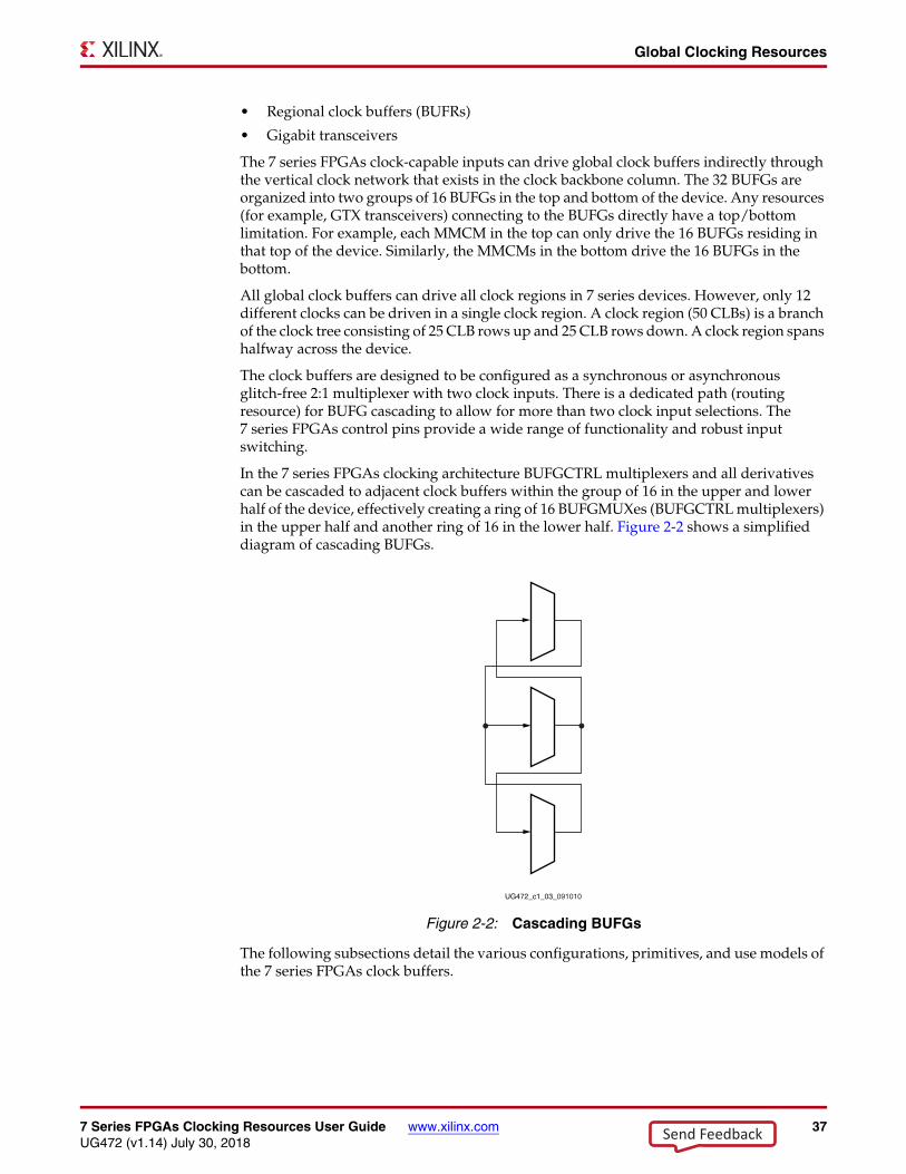
Each 7 series monolithic device has 32 global clock lines that can clock and provide control signals to all sequential resources in the whole device. Global clock buffers (BUFGCTRL, simplified as BUFG throughout this user guide) drive the global clock lines and must be used to access global clock lines. Each clock region can support up to 12 of these global clock lines using the 12 horizontal clock lines in the clock region.
The global clock buffers:
• Can be used as a clock enable circuit to enable or disable clocks that span multiple clock regions
• Can be used as a glitch-free multiplexer to:
• select between two clock sources
• switch away from a failed clock source
• Are often driven by a CMT to:
• eliminate the clock distribution delay
• adjust clock delay relative to another clock
The horizontal clock buffer (BUFH/BUFHCE) allows access to the global clock lines in a single clock region through the horizontal clock row. It can also be used as a clock enable circuit (BUFHCE) to independently enable or disable clocks that span a single clock region. Each clock region can support up to 12 clocks using the 12 horizontal clock lines in each clock region.
Each 7 series FPGA has regional and I/O clock trees that can clock all sequential resources in one clock region. Each device also has multi-clock region buffers (BUFMR) that allow regional and I/O clocks to span up to three vertically adjacent clock regions.
• The I/O clock buffer (BUFIO) drives the I/O clock tree, providing access to clock all sequential I/O resources in the same I/O bank.
• The regional clock buffer (BUFR) drives regional clock trees that drive all clock destinations in the same clock region and can be programmed to divide the incoming clock rate.
• In conjunction with the programmable serializer/deserializer in the IOB (refer to the Advanced SelectIO Logic Resources chapter in UG471, 7 Series FPGAs SelectIO Resources User Guide), the BUFIO and BUFR clock buffers allow source-synchronous systems to cross clock domains without using additional logic resources.
• The regional and I/O clock trees in adjacent clock regions and I/O banks can be driven using the multi-clock region buffer (BUFMR) when used with the associated BUFR or BUFIO.
• Up to four unique I/O clocks and four unique regional clocks can be supported in one clock region or I/O bank.
High-performance clock routing connects certain outputs of the CMT to the I/O on a very low jitter, minimal duty-cycle distorted direct path.
Chapter 2, Clock Routing Resources, has further details on global, regional, and I/O clocks. It also describes which clock routing resources to use for various applications.
CMT OverviewEach 7 series FPGA has up to 24 CMTs, each consisting of one MMCM and one PLL. The MMCMs and PLLs serve as frequency synthesizers for a wide range of frequencies, serve as a jitter filters for either external or internal clocks, and deskew clocks. The PLL contains
Send Feedback
7 Series FPGAs Clocking Resources User Guide www.xilinx.com 15UG472 (v1.14) July 30, 2018
Clocking Architecture Overview
a subset of the MMCM functions. The 7 series FPGA clock input connectivity allows multiple resources to provide the reference clocks to the MMCM and PLL.
7 series FPGAs MMCMs have infinite fine phase-shift capability in either direction and can be used in dynamic phase-shift mode. MMCMs also have a fractional counter in either the feedback path or in one output path, enabling further granularity of frequency synthesis capabilities.
The LogiCORE™ IP clocking wizard is available to assist in utilizing MMCMs and PLLs to create clock networks in 7 series FPGA designs. The GUI interface is used to collect clock network parameters. The clocking wizard chooses the appropriate CMT resource and optimally configures the CMT resource and associated clock routing resources.
Chapter 3, Clock Management Tile, includes details on the CMT block features and connectivity.
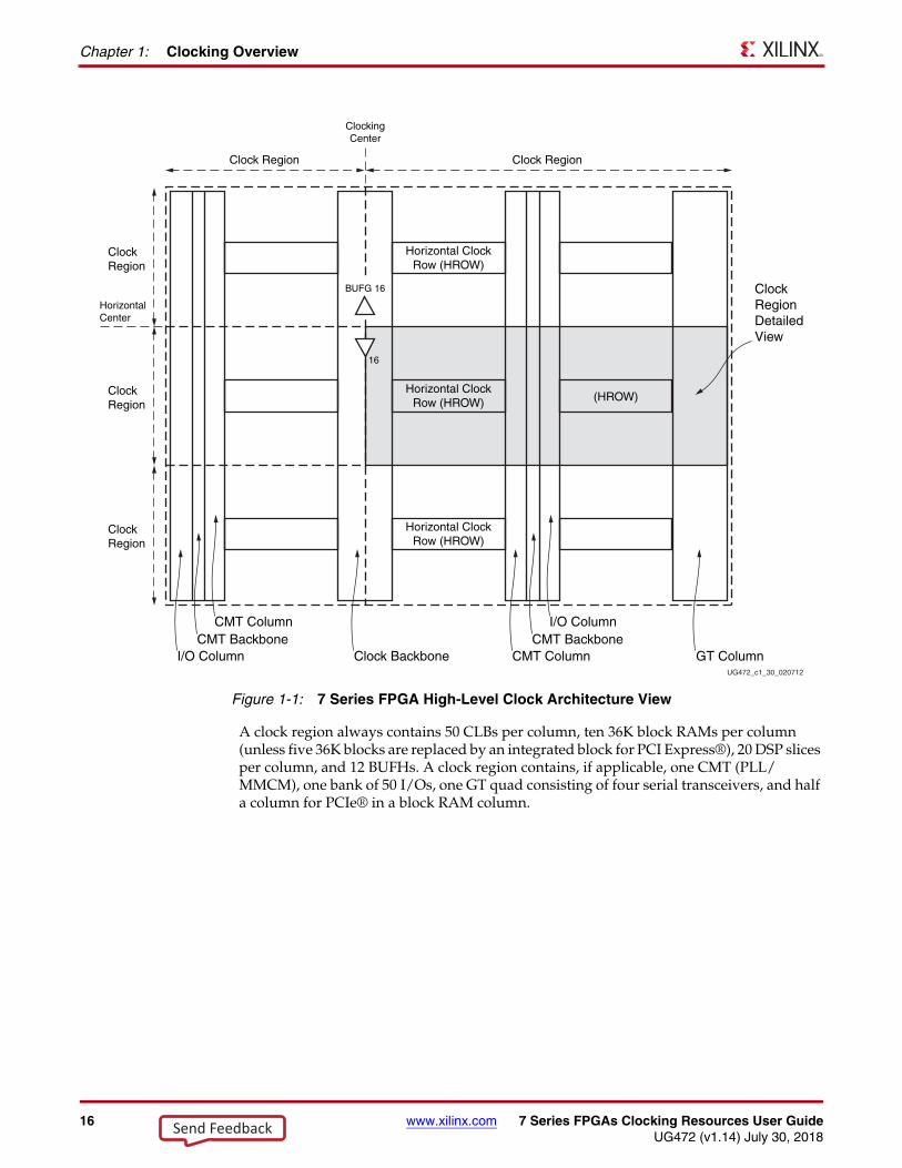
Clock Buffers, Management, and RoutingThe figures in this section provide a visual and layered explanation of the 7 series FPGAs clock architecture.
Figure 1-1 is a high-level view of the 7 series FPGAs clocking architecture. The vertical clocking center line (the clock backbone) divides the device into adjacent left and right regions while the horizontal center line divides the device into its top and bottom sides. The resources in the clock backbone are mirrored to both sides of the horizontally adjacent regions, thus extending certain clock resources into the horizontal adjacent region. The top and bottom division separates two sets of global clock buffers (BUFGs) and imposes some limitations on how they can be connected. However, BUFGs do not belong to a clock region and can reach any clocking point on the device. All horizontal clock resources are contained in the center of the clock region horizontal clock row (HROW), and vertical, non-regional clock resources are contained in either the clock backbone or CMT backbone.
Send Feedback
16 www.xilinx.com 7 Series FPGAs Clocking Resources User GuideUG472 (v1.14) July 30, 2018
Chapter 1: Clocking Overview
A clock region always contains 50 CLBs per column, ten 36K block RAMs per column (unless five 36K blocks are replaced by an integrated block for PCI Express®), 20 DSP slices per column, and 12 BUFHs. A clock region contains, if applicable, one CMT (PLL/MMCM), one bank of 50 I/Os, one GT quad consisting of four serial transceivers, and half a column for PCIe® in a block RAM column.
X-Ref Target - Figure 1-1
Figure 1-1: 7 Series FPGA High-Level Clock Architecture View
UG472_c1_30_020712
I/O Column Clock BackboneCMT Backbone
CMT Column
Clock Region Clock Region
ClockingCenter
HorizontalCenter
Horizontal ClockRow (HROW)
Horizontal ClockRow (HROW)
Horizontal ClockRow (HROW)
(HROW)
CMT Column GT ColumnCMT Backbone
I/O Column
BUFG 16
16
ClockRegionDetailedView
ClockRegion
ClockRegion
ClockRegion
Send Feedback
7 Series FPGAs Clocking Resources User Guide www.xilinx.com 17UG472 (v1.14) July 30, 2018
Clocking Architecture Overview
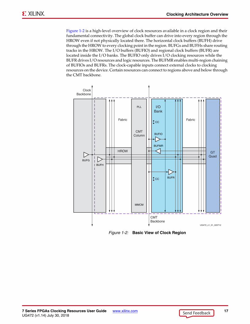
Figure 1-2 is a high-level overview of clock resources available in a clock region and their fundamental connectivity. The global clock buffer can drive into every region through the HROW even if not physically located there. The horizontal clock buffers (BUFH) drive through the HROW to every clocking point in the region. BUFGs and BUFHs share routing tracks in the HROW. The I/O buffers (BUFIO) and regional clock buffers (BUFR) are located inside the I/O banks. The BUFIO only drives I/O clocking resources while the BUFR drives I/O resources and logic resources. The BUFMR enables multi-region chaining of BUFIOs and BUFRs. The clock-capable inputs connect external clocks to clocking resources on the device. Certain resources can connect to regions above and below through the CMT backbone.X-Ref Target - Figure 1-2
Figure 1-2: Basic View of Clock Region
UG472_c1_31_020712
ClockBackbone
CMTBackbone
CMTColumn
GTQuad
I/OBank
PLL
MMCM
HROW
Fabric Fabric
BUFG
BUFH
BUFMR
BUFR
BUFIO
CC
CC
Send Feedback
18 www.xilinx.com 7 Series FPGAs Clocking Resources User GuideUG472 (v1.14) July 30, 2018
Chapter 1: Clocking Overview
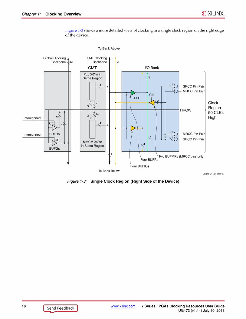
Figure 1-3 shows a more detailed view of clocking in a single clock region on the right edge of the device.
X-Ref Target - Figure 1-3
Figure 1-3: Single Clock Region (Right Side of the Device)
Global ClockingBackbone 32 2
12
12
3
3
7
14
4
2
1
1
1
1
4
4
4
4
4
BUFHs
CLR
I/O Bank
CE
CE
CE
PLL X0Yn inSame Region
MMCM X0Ynin Same Region
BUFGs
CMT ClockingBackbone
CMT
Interconnect
Interconnect
ClockRegion50 CLBsHigh
SRCC Pin Pair
MRCC Pin Pair
MRCC Pin Pair
SRCC Pin Pair
To Bank Above
To Bank Below
Four BUFRs
Four BUFIOs
Two BUFMRs (MRCC pins only)
HROW
UG472_c1_32_011713
Send Feedback
7 Series FPGAs Clocking Resources User Guide www.xilinx.com 19UG472 (v1.14) July 30, 2018
Clocking Architecture Overview
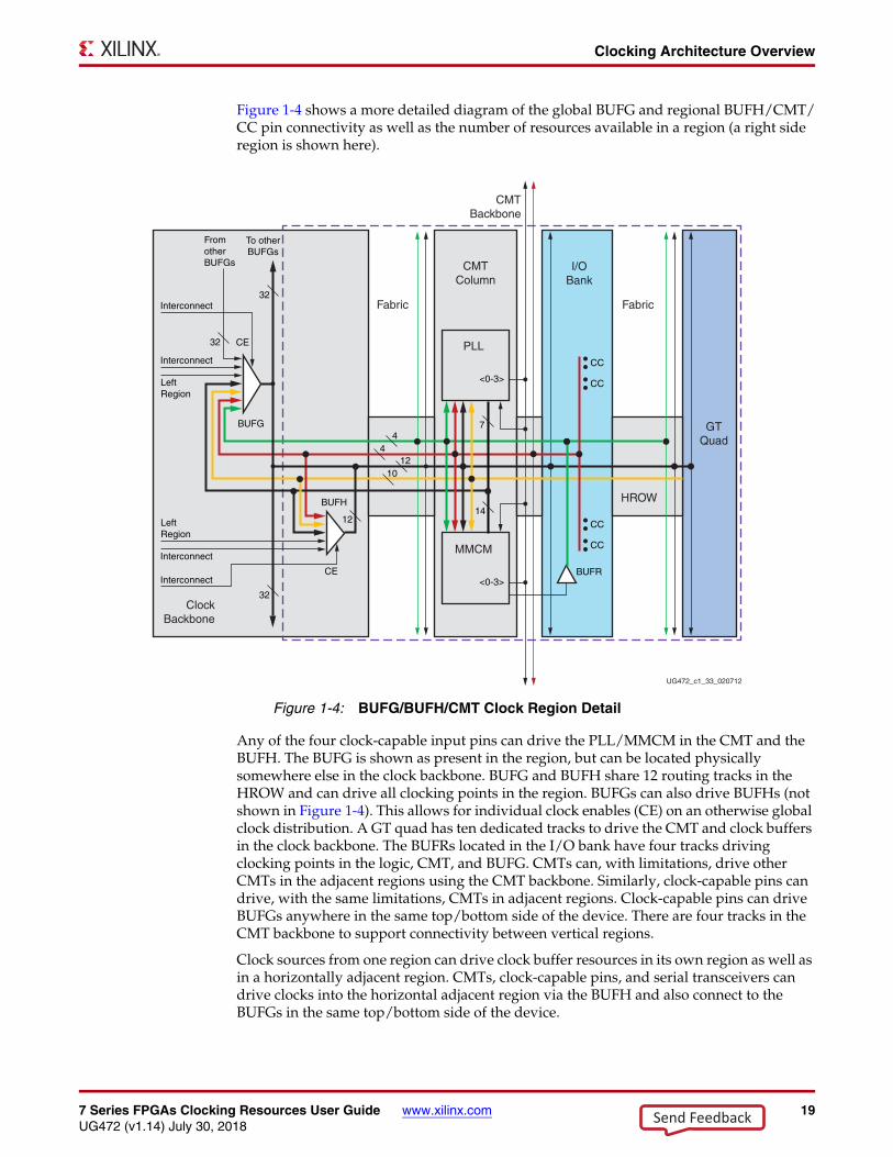
Figure 1-4 shows a more detailed diagram of the global BUFG and regional BUFH/CMT/CC pin connectivity as well as the number of resources available in a region (a right side region is shown here).
Any of the four clock-capable input pins can drive the PLL/MMCM in the CMT and the BUFH. The BUFG is shown as present in the region, but can be located physically somewhere else in the clock backbone. BUFG and BUFH share 12 routing tracks in the HROW and can drive all clocking points in the region. BUFGs can also drive BUFHs (not shown in Figure 1-4). This allows for individual clock enables (CE) on an otherwise global clock distribution. A GT quad has ten dedicated tracks to drive the CMT and clock buffers in the clock backbone. The BUFRs located in the I/O bank have four tracks driving clocking points in the logic, CMT, and BUFG. CMTs can, with limitations, drive other CMTs in the adjacent regions using the CMT backbone. Similarly, clock-capable pins can drive, with the same limitations, CMTs in adjacent regions. Clock-capable pins can drive BUFGs anywhere in the same top/bottom side of the device. There are four tracks in the CMT backbone to support connectivity between vertical regions.
Clock sources from one region can drive clock buffer resources in its own region as well as in a horizontally adjacent region. CMTs, clock-capable pins, and serial transceivers can drive clocks into the horizontal adjacent region via the BUFH and also connect to the BUFGs in the same top/bottom side of the device.
X-Ref Target - Figure 1-4
Figure 1-4: BUFG/BUFH/CMT Clock Region Detail
UG472_c1_33_020712
ClockBackbone
CMTBackbone
CMTColumn
GTQuad
I/OBank
PLL
<0-3>
MMCM
<0-3>
HROW
Fabric Fabric
BUFG
BUFH
BUFR
CE
CE
Interconnect
FromotherBUFGs
Interconnect
Interconnect
LeftRegion
LeftRegion
Interconnect
To otherBUFGs
CC
CC
32
32
32
4
12
412
10
CC
CC
7
14
Send Feedback
20 www.xilinx.com 7 Series FPGAs Clocking Resources User GuideUG472 (v1.14) July 30, 2018
Chapter 1: Clocking Overview
Logic interconnects drive the CE pins of BUFG and BUFH. Logic interconnects can also drive clocks into the same buffers, but care must be taken because the timing is not predictable.
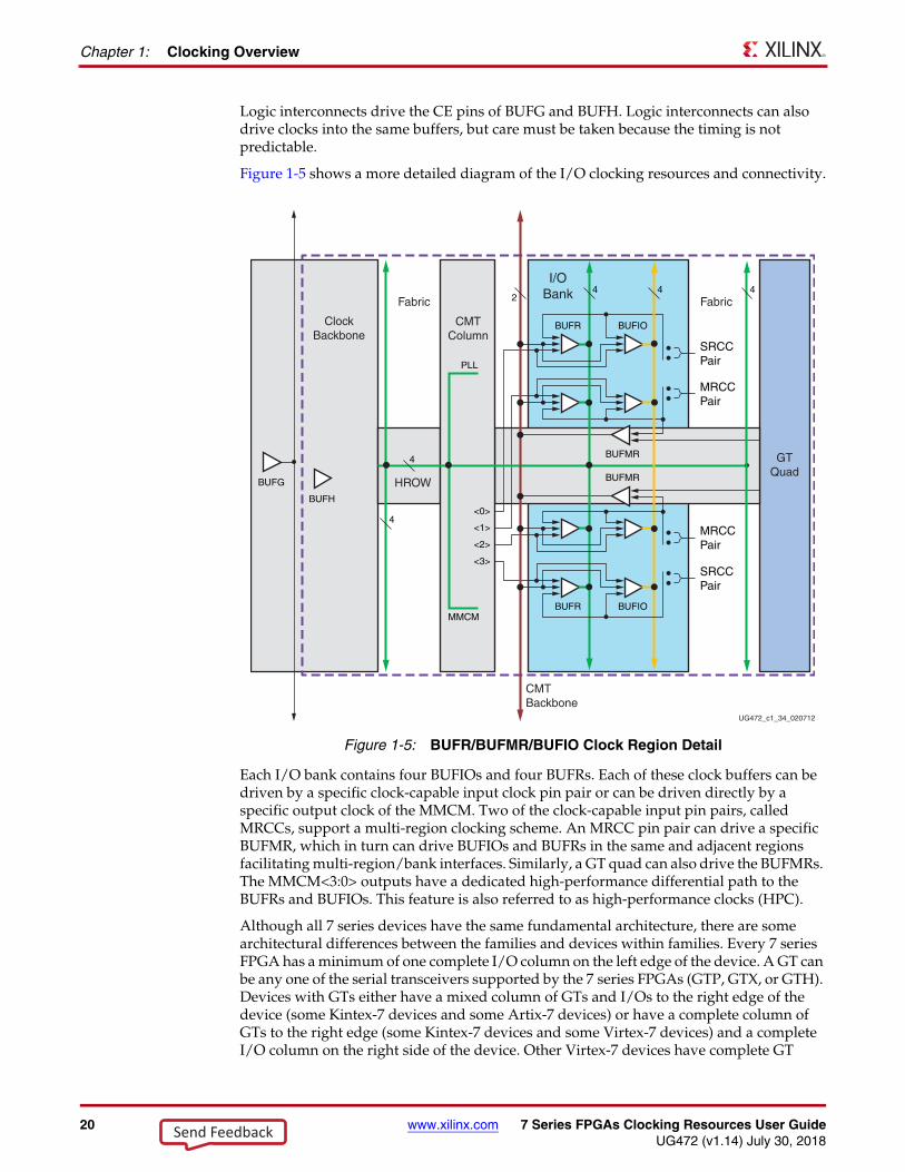
Figure 1-5 shows a more detailed diagram of the I/O clocking resources and connectivity.
Each I/O bank contains four BUFIOs and four BUFRs. Each of these clock buffers can be driven by a specific clock-capable input clock pin pair or can be driven directly by a specific output clock of the MMCM. Two of the clock-capable input pin pairs, called MRCCs, support a multi-region clocking scheme. An MRCC pin pair can drive a specific BUFMR, which in turn can drive BUFIOs and BUFRs in the same and adjacent regions facilitating multi-region/bank interfaces. Similarly, a GT quad can also drive the BUFMRs. The MMCM<3:0> outputs have a dedicated high-performance differential path to the BUFRs and BUFIOs. This feature is also referred to as high-performance clocks (HPC).
Although all 7 series devices have the same fundamental architecture, there are some architectural differences between the families and devices within families. Every 7 series FPGA has a minimum of one complete I/O column on the left edge of the device. A GT can be any one of the serial transceivers supported by the 7 series FPGAs (GTP, GTX, or GTH). Devices with GTs either have a mixed column of GTs and I/Os to the right edge of the device (some Kintex-7 devices and some Artix-7 devices) or have a complete column of GTs to the right edge (some Kintex-7 devices and some Virtex-7 devices) and a completeI/O column on the right side of the device. Other Virtex-7 devices have complete GT
X-Ref Target - Figure 1-5
Figure 1-5: BUFR/BUFMR/BUFIO Clock Region Detail
UG472_c1_34_020712
ClockBackbone
CMTBackbone
CMTColumn
GTQuad
I/OBank
PLL
MMCM
HROW
Fabric Fabric
BUFG
BUFH
BUFR BUFIO
BUFR BUFIO
BUFMR
BUFMR
4
4
4 4 42
<0>
<1>
<2>
<3>
SRCCPair
MRCCPair
MRCCPair
SRCCPair
Send Feedback
7 Series FPGAs Clocking Resources User Guide www.xilinx.com 21UG472 (v1.14) July 30, 2018
7 Series FPGAs Clocking Differences from Previous FPGA Generations
columns on the left and right edges with a complete I/O column in the left and right sides. The Artix-7 200T device has GTP transceivers on the top and bottom next to the clocking column.
Therefore, not all clock regions in 7 series devices contain all of the blocks shown in the previous figures. For a block-level architectural view of the 7 series devices, see the Die Level Bank Numbering Overview section in UG475, 7 Series FPGA Packaging and Pinout Specification. Appendix B, Clocking Resources and Connectivity Variations per Clock Region includes detailed figures showing clocking resources and connectivity for the clock region variations.
7 Series FPGAs Clocking Differences from Previous FPGA Generations
The 7 series FPGAs clocking has a similar structure to Virtex-6 FPGAs and supports many of the same features. However, there are some architectural differences and modifications to the various clocking elements and their functionality. When compared with Spartan-6 FPGAs, there are some significant changes in both architecture and functionality. Some Spartan-6 FPGA clock primitives are no longer available and are replaced by more powerful and simpler structures.
Key Differences from Virtex-6 FPGAs• The 7 series FPGAs basic BUFIO clocking functions have not changed with the
exception that the BUFIO now only spans a single bank. Direct clocking of adjacent banks is replaced by a new clock buffer. There are now four BUFIOs per bank. Similar to the BUFIO evolution, the basic purpose of the BUFR has not changed. However, now the BUFR only directly spans a single clock region. There are now four BUFRs and four regional clocks (tracks) per region.
• The 7 series FPGAs introduced a new buffer type: BUFMR/BUFMRCE. The BUFMR/BUFMRCEs drive BUFIOs and/or BUFRs in the same and vertically adjacent regions. They also provide the same multi-clock region/multi-bank clock routing available in Virtex-6 FPGAs which support the same three clock regions/banks capability. BUFMRCE has a selectable synchronous or asynchronous switching feature.
• The global clock (GC) input pins in the Virtex-6 family are no longer supported by the 7 series FPGAs. Four clock-capable clock input pin/pairs per bank replace the GCs. The connectivity of the clock-capable input pins has been enhanced to support much of the previous GC capabilities.
• The global clock multiplexer BUFGMUX has added an attribute, CLK_SEL_TYPE, for allowing either synchronous or asynchronous clock switching of the two input clocks (previously only available through the IGNORE port).
• The BUFHCE has an enhanced clock enable to allow for either a synchronous or asynchronous enable of the input clock.
• The CMT now contains one MMCM and one PLL (a subset of the MMCM), instead of two MMCMs, and dedicated memory interface logic, which is reserved. The CMT column is located adjacent to the SelectIO™ columns/banks within the CMT and has dedicated access to the I/Os for high performance. The global clock buffers are still located in the vertical center of the device between I/O columns driven by the CMTs. Direct cascading within the CMT is no longer supported. Cascading to adjacent CMTs directly is possible but limited due to limited resources. Cascading to other CMTs
Send Feedback
22 www.xilinx.com 7 Series FPGAs Clocking Resources User GuideUG472 (v1.14) July 30, 2018
Chapter 1: Clocking Overview
beyond the adjacent CMTs results in a phase offset between the source and destination MMCMs/PLLs and requires a special attribute setting.
• Fractional dividers no longer share output counters. This frees up those counters for other uses. Fractional counters have added a static phase-shift capability.
• The CLOCK_HOLD feature is no longer available.
• MMCMs support spread spectrum.
Key Differences from Spartan-6 FPGAs• Some of the Spartan-6 FPGA clocking circuit topologies, functions, and blocks that are
unique to the Spartan-6 architecture are not supported and have been replaced by the 7 series FPGAs clocking features. Features and functions such as DCM_SP, DCM_CLKGEN, BUFIO2, BUFIO2_2CLK, BUFIO2FB, BUFPLL, and BUFPLL_MCB are not directly supported in 7 series devices.
• The PLL is a subset of the MMCM with the same performance (except minimum CLKIN/PFD and minimum/maximum VCO frequencies), some connectivity limitations, and some reduced functionality. When compared to previous Spartan® FPGA PLLs, the 7 series FPGAs PLLs add power down, input clock switching, and cascading to adjacent CMTs. The PLLs do not have a direct connection to the BUFIO or BUFR.
• In the 7 series FPGAs, there is no direct replacement for the BUFIO2 and BUFIO2_2CLK primitives. Use the BUFIO and BUFR instead with the recommended connections to drive the ILOGIC and OLOGIC.
• The Spartan-6 FPGA BUFIO2 dedicated input routing from GCLKs to the CMT and global clock buffers are no longer supported. To migrate to the 7 series FPGAs, use the dedicated input routing from the CCIO pins.
• There is no direct equivalent in the 7 series FPGAs to the Spartan-6 FPGA BUFPLL. To migrate, use the BUFIO and BUFR with the recommended connections to the ILOGIC and OLOGIC. The high-performance clock routing from MMCME2 CLKOUT[0:3] replaces the dedicated routing to the BUFPLL. The ISERDES and OSERDES circuitry is based on the Virtex-6 architecture. See UG471: 7 Series FPGAs SelectIO Resources User Guide.
• In the 7 series FPGAs, the BUFPLL_MCB primitive is no longer required. DDR memory interfaces have a different (soft) implementation in the 7 series FPGAs. Consult the UG586: Memory Interface Solutions User Guide.
• In the 7 series FPGAs, the BUFIO2FB primitive is no longer required. For MMCM and PLL feedback connections the CLKFBIN can be directly connected to global clock buffers, input pins, or CLKFBOUT depending on the feedback used.
• Spartan-6 FPGAs only supported BUFH. The 7 series FPGAs BUFHCE primitive adds the ability to disable the clock for potential power savings in the clock region driven by this resource.
• The 7 series FPGAs new buffers, BUFMR/BUFMRCE, drive BUFIOs and/or BUFRs in the same and vertically adjacent clock regions. When used with a BUFIO or BUFR, BUFMR/BUFMRCE allow MRCC inputs to access BUFIO and BUFR in adjacent clock regions. BUFMRCE has a selectable synchronous or asynchronous switching feature.
• A new primitive for Spartan-6 FPGA design migration is the BUFR. When used in conjunction with BUFIO the BUFRs functionality replaces the BUFIO2, BUFIO2_2CLK, and BUFPLL capabilities. There are four BUFRs in each clock region.
Send Feedback
7 Series FPGAs Clocking Resources User Guide www.xilinx.com 23UG472 (v1.14) July 30, 2018
7 Series FPGAs Clocking Differences from Previous FPGA Generations
• Another new primitive for Spartan-6 FPGA design migration is the BUFIO. When used with the BUFR, the BUFIO functionality replaces the BUFIO2, BUFIO2_2CLK, and BUFPLL capabilities. There are four BUFIOs per bank.
• Instead of two DCMs and one PLL in the Spartan-6 architecture, the 7 series FPGAs use a CMT that contains one MMCM, one PLL, and dedicated memory interface logic which is reserved for Xilinx use at this time. DCMs and their associated capabilities are now supported with these functions. The CMTs are located in a separate column adjacent to the SelectIO columns and have dedicated access to the I/O. DCM_SP and DCM_CLKGEN are no longer available and their functionality is now supported in the MMCMs and PLLs.
• Global clock (GCLK) inputs are no longer supported in the 7 series FPGAs. Four clock-capable input pins are now available in every bank that support much of the Spartan-6 FPGA GCLK pin capabilities.
• To Spartan-6 FPGA designers, the MMCM is a new functional block. The MMCM adds fractional divide, fine phase shifting, dynamic phase shifting, inverted clock outputs, CLKOUT6 to CLKOUT4 cascading, and some other features. The direct routing connection to the BUFPLL is replaced by the HPC connection from the MMCMs to the BUFIO/BUFR using CLKOUT[0:3]. A more extensive DRP is also available.
• Using the PLL is no longer the recommended CMT function for general-purpose high-speed I/O clocking. The PLL does not have a direct connection to the BUFIO or BUFR. CLKOUT0 feedback is no longer supported. Use the MMCM for high-speed I/O interfaces. Cascade connections use limited CMT backbone resources. There is also a new power down mode. Input clock switching is fully supported. Operating ranges are different between the Spartan-6 FPGAs and the 7 series FPGAs. The DRP functionality is still available. The DRP functional locations and addresses have changed.
• The Spartan-6 FPGAs DCM_SP is no longer supported. To migrate to the 7 series FPGAs, use the MMCM and PLL.
• The Spartan-6 FPGAs DCM_CLKGEN is not directly supported in the 7 series FPGAs. Use MMCM or PLL with low bandwidth for input jitter filtering. Dynamic reprogramming of the M/D values can also be accomplished using the DRP reference design for the MMCM or PLL.
Send Feedback
24 www.xilinx.com 7 Series FPGAs Clocking Resources User GuideUG472 (v1.14) July 30, 2018
Chapter 1: Clocking Overview
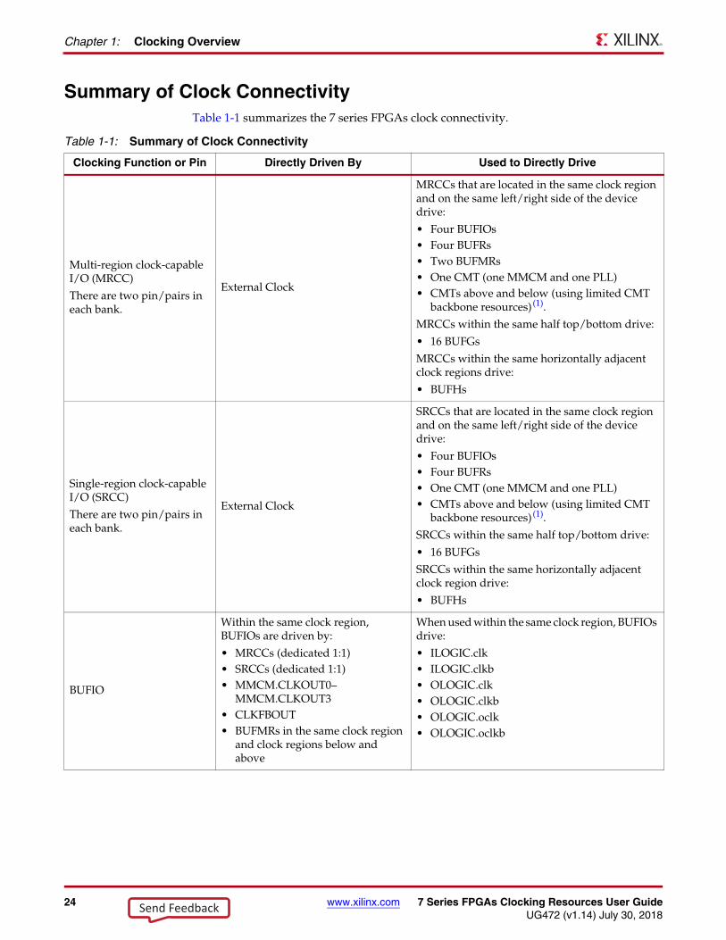
Summary of Clock ConnectivityTable 1-1 summarizes the 7 series FPGAs clock connectivity.
Table 1-1: Summary of Clock Connectivity
Clocking Function or Pin Directly Driven By Used to Directly Drive
Multi-region clock-capable I/O (MRCC)
There are two pin/pairs in each bank.
External Clock
MRCCs that are located in the same clock region and on the same left/right side of the device drive:
• Four BUFIOs• Four BUFRs• Two BUFMRs• One CMT (one MMCM and one PLL)• CMTs above and below (using limited CMT
backbone resources)(1).
MRCCs within the same half top/bottom drive:
• 16 BUFGs
MRCCs within the same horizontally adjacent clock regions drive:
• BUFHs
Single-region clock-capable I/O (SRCC)
There are two pin/pairs in each bank.
External Clock
SRCCs that are located in the same clock region and on the same left/right side of the device drive:
• Four BUFIOs• Four BUFRs• One CMT (one MMCM and one PLL)• CMTs above and below (using limited CMT
backbone resources)(1).
SRCCs within the same half top/bottom drive:
• 16 BUFGs
SRCCs within the same horizontally adjacent clock region drive:
• BUFHs
BUFIO
Within the same clock region, BUFIOs are driven by:
• MRCCs (dedicated 1:1)• SRCCs (dedicated 1:1)• MMCM.CLKOUT0–
MMCM.CLKOUT3• CLKFBOUT• BUFMRs in the same clock region
and clock regions below and above
When used within the same clock region, BUFIOs drive:
• ILOGIC.clk• ILOGIC.clkb• OLOGIC.clk• OLOGIC.clkb• OLOGIC.oclk• OLOGIC.oclkb
Send Feedback
7 Series FPGAs Clocking Resources User Guide www.xilinx.com 25UG472 (v1.14) July 30, 2018
Summary of Clock Connectivity
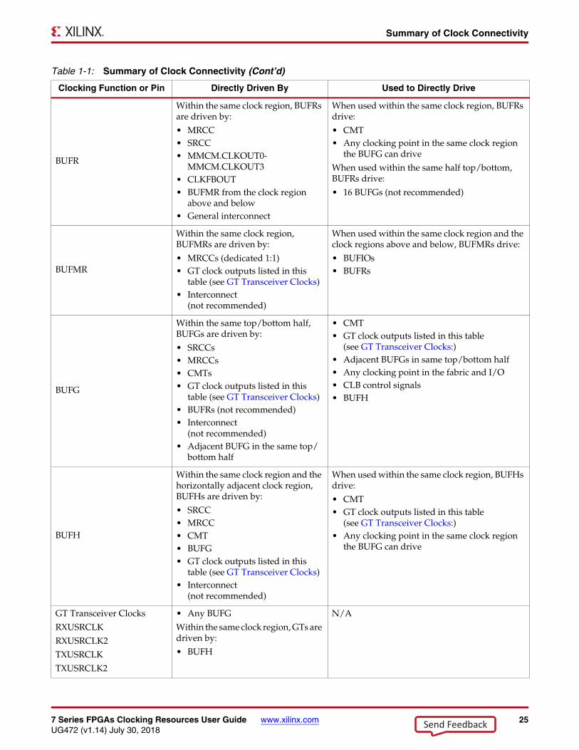
BUFR
Within the same clock region, BUFRs are driven by:
• MRCC• SRCC• MMCM.CLKOUT0-
MMCM.CLKOUT3• CLKFBOUT• BUFMR from the clock region
above and below• General interconnect
When used within the same clock region, BUFRs drive:
• CMT• Any clocking point in the same clock region
the BUFG can drive
When used within the same half top/bottom, BUFRs drive:
• 16 BUFGs (not recommended)
BUFMR
Within the same clock region, BUFMRs are driven by:
• MRCCs (dedicated 1:1)• GT clock outputs listed in this
table (see GT Transceiver Clocks)• Interconnect
(not recommended)
When used within the same clock region and the clock regions above and below, BUFMRs drive:
• BUFIOs• BUFRs
BUFG
Within the same top/bottom half, BUFGs are driven by:
• SRCCs• MRCCs• CMTs• GT clock outputs listed in this
table (see GT Transceiver Clocks)• BUFRs (not recommended)• Interconnect
(not recommended)• Adjacent BUFG in the same top/
bottom half
• CMT• GT clock outputs listed in this table
(see GT Transceiver Clocks:)• Adjacent BUFGs in same top/bottom half• Any clocking point in the fabric and I/O• CLB control signals• BUFH
BUFH
Within the same clock region and the horizontally adjacent clock region, BUFHs are driven by:
• SRCC• MRCC• CMT• BUFG• GT clock outputs listed in this
table (see GT Transceiver Clocks)• Interconnect
(not recommended)
When used within the same clock region, BUFHs drive:
• CMT• GT clock outputs listed in this table
(see GT Transceiver Clocks:)• Any clocking point in the same clock region
the BUFG can drive
GT Transceiver Clocks
RXUSRCLK
RXUSRCLK2
TXUSRCLK
TXUSRCLK2
• Any BUFG
Within the same clock region, GTs are driven by:
• BUFH
N/A
Table 1-1: Summary of Clock Connectivity (Cont’d)
Clocking Function or Pin Directly Driven By Used to Directly Drive
Send Feedback
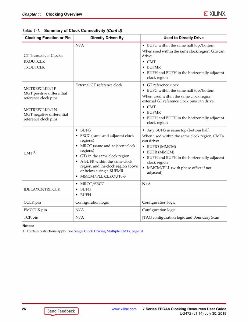
26 www.xilinx.com 7 Series FPGAs Clocking Resources User GuideUG472 (v1.14) July 30, 2018
Chapter 1: Clocking Overview
GT Transceiver Clocks:
RXOUTCLK
TXOUTCLK
N/A • BUFG within the same half top/bottom
When used within the same clock region, GTs can drive:
• CMT• BUFMR• BUFH and BUFH in the horizontally adjacent
clock region
MGTREFCLK0/1PMGT positive differential reference clock pins
MGTREFCLK0/1NMGT negative differential reference clock pins
External GT reference clock • GT reference clock• BUFG within the same half top/bottom
When used within the same clock region, external GT reference clock pins can drive:
• CMT• BUFMR• BUFH and BUFH in the horizontally adjacent
clock region
CMT(1)
• BUFG• SRCC (same and adjacent clock
regions)• MRCC (same and adjacent clock
regions)• GTs in the same clock region• A BUFR within the same clock
region, and the clock region above or below using a BUFMR
• MMCM/PLL.CLKOUT0-3
• Any BUFG in same top/bottom half
When used within the same clock region, CMTs can drive:
• BUFIO (MMCM)• BUFR (MMCM)• BUFH and BUFH in the horizontally adjacent
clock region• MMCM/PLL (with phase offset if not
adjacent)
IDELAYCNTRL.CLK• MRCC/SRCC• BUFG• BUFH
N/A
CCLK pin Configuration logic Configuration logic
EMCCLK pin N/A Configuration logic
TCK pin N/A JTAG configuration logic and Boundary Scan
Notes: 1. Certain restrictions apply. See Single Clock Driving Multiple CMTs, page 31.
Table 1-1: Summary of Clock Connectivity (Cont’d)
Clocking Function or Pin Directly Driven By Used to Directly Drive
Send Feedback
7 Series FPGAs Clocking Resources User Guide www.xilinx.com 27UG472 (v1.14) July 30, 2018
Summary of Clock Connectivity
Clocking Differences in 7 Series FPGAsEach of the 7 series FPGA families have some unique connectivity requirements. Table 1-2 lists the connectivity limitations described in Table 1-1 by device family. For a comprehensive graphical representation of the GT, CMT, and I/O locations and alignments, see the Die Level Bank Numbering Overview section in UG475, 7 Series FPGA Packaging and Pinout Specification.
Table 1-2: Clocking Connectivity Differences by 7 Series FPGAs
Family Exceptions
Spartan-7 FPGAs:
All devices
There are no connectivity exceptions.
Artix-7 FPGAs:
All devices
There are no direct connections from the GTP transceivers to the CMTs and BUFMRs. When connecting from the GTP transceivers to a CMT, a BUFH or BUFG is required.
Kintex-7 FPGAs:
All devices
There are no direct connections from the GTX transceivers to the CMTs and BUFMRs. When connecting from the GTX transceivers to a CMT, a BUFH or BUFG is required.
All Virtex-7 T and XT FPGAs
There are no connectivity exceptions. See Stacked Silicon Interconnect Clocking in Chapter 2 for clocking guidelines when designing with the XC7V2000T and XC7VX1140T devices.
All Virtex-7 HT FPGAs
GTZ transceivers can only connect to the interposer clock backbone to connect to SLRs. Thus, they can only drive global clock networks (BUFG routing tracks) and BUFHs and can only be driven by BUFGs. See Stacked Silicon Interconnect Clocking in Chapter 2.
Send Feedback
28 www.xilinx.com 7 Series FPGAs Clocking Resources User GuideUG472 (v1.14) July 30, 2018
Chapter 1: Clocking Overview
Send Feedback
7 Series FPGAs Clocking Resources User Guide www.xilinx.com 29UG472 (v1.14) July 30, 2018
Chapter 2
Clock Routing Resources
7 series FPGAs have several clock routing resources to support various clocking schemes and requirements, including high fanout, short propagation delay, and extremely low skew. To best utilize the clock routing resources, you must understand how to get user clocks from the PCB to the FPGA, decide which clock routing resources are optimal, and then access those clock routing resources by utilizing the appropriate I/O and clock buffers.
This chapter covers:
• Clock Buffer Selection Considerations
• Clock-Capable Inputs
• Global Clocking Resources
• Regional Clocking Resources
• High-Performance Clocks
Clock Buffer Selection Considerations7 series FPGAs have a rich set of clocking resources. The various buffer types, clock input pins, and clocking connectivity satisfy many different application requirements. Selecting the proper clocking resources can improve routeability, performance, and general FPGA resource utilization. For some applications and designs, floor planning or other types of manual guidance can also greatly impact the implementation.
BUFGCTRL (most often used as a BUFG) is the most commonly used clock routing resource. These truly global clocks can connect to every clocking point on the device. However, in some cases it is more advantageous to use alternate clocking buffers for either performance, functional, or clocking resource availability reasons. BUFGs are best deployed when:
• Designs or portions of a design have global reach across large areas of the device and localization of functions is not possible.
• Hardware functional blocks such as block RAM, DSP, or integrated IP that spans many clock regions, are cascaded, or need connections to CLBs that are not nearby.
• By switching clocks synchronous (glitch free) or asynchronous, applications are able to switch away from a stopped clock or select a clock with a different frequency (for example, power reduction).
• The clock enable (CE) functionality can be used to reduce power during non-operating periods. However, in most cases, the CE capability should not be used to simulate a true CE logic function at the clocking elements due to timing (CE delay) limitations.
Send Feedback
30 www.xilinx.com 7 Series FPGAs Clocking Resources User GuideUG472 (v1.14) July 30, 2018
Chapter 2: Clock Routing Resources
• The CE function can be used to synchronize initialized clocking elements after device startup.
The main purpose of the BUFR and BUFIO combination is to support source-synchronous interfaces. When an interface is placed into a single region, the BUFIO clocks the high-speed side of the SelectIOs and the BUFR clocks the deserialized/serialized side at a lower speed into the FPGA logic providing the clock domain transfer function. For interfaces that require more logic and/or I/Os than are available in a single clock region/bank, the BUFMR (BUFMRCE) is used to expand clock domain transfer functionality into the clock regions above and below. Certain types of applications that require a divided clock not related to the source-synchronous I/O use case can use a BUFR as a simple clock divider when an MMCM/PLL cannot be used or is not available for the frequency divide function. In this case, particular attention must be paid to the timing and skew because this is not the primary purpose of the BUFR. For more information on clocking SelectIO resources, consult UG471, 7 Series FPGAs SelectIO Resources User Guide.
The horizontal clock buffer BUFH (BUFHCE) is strictly a regional resource and cannot span clock regions above or below. Unlike BUFR, BUFH does not have the ability to divide the clock.
• BUFHs are similar to a global clocking resource only on a regional basis spanning two horizontal regions.
• BUFHs have the ability to serve as a feedback to the MMCM/PLL and the clock insertion delay can be compensated for.
• BUFHs are the preferred clocking resource when an interface or cloud of logic can be localized to one clock region or two horizontally adjacent clock regions.
• The BUFH also has a clock enable pin (BUFHCE) that can be used to reduce dynamic power consumption when either the logic or an interface and its associated logic are not active.
• The clock enable feature can provide a gated clock on a clock cycle-to-cycle basis.
• Similar to the global clock tree, the BUFH can also connect to non-clocking resources in the CLB (enable/reset) but with better skew characteristics.
• BUFH can also be used for the synchronous startup of clocking elements in a clock region.
For stacked silicon interconnect (SSI) device limitations with respect to clocking resource selection, see Stacked Silicon Interconnect Clocking.
Clock-Capable InputsExternal user clocks must be brought into the FPGA on differential clock pin pairs called clock-capable (CC) inputs. Clock-capable inputs provide dedicated, high-speed access to the internal global and regional clock resources. Clock-capable inputs use dedicated routing and must be used for clock inputs to guarantee timing of various clocking features. General-purpose I/O with local interconnects should not be used for clock signals.
Each I/O bank is located in a single clock region and includes 50 I/O pins. Of the 50 I/O pins in each I/O bank in every I/O column, there are four clock-capable input pin pairs (a total of eight pins). Each clock-capable input:
• Can be connected to a differential or single-ended clock on the PCB
• Can be configured for any I/O standard, including differential I/O standards
• Has a P-side (master), and an N-side (slave)
Send Feedback
7 Series FPGAs Clocking Resources User Guide www.xilinx.com 31UG472 (v1.14) July 30, 2018
Clock-Capable Inputs
Single-ended clock inputs must be assigned to the P (master) side of the clock-capable input pin pair.
If a single-ended clock is connected to the P-side of a differential clock pin pair, the N-side cannot be used as another single-ended clock pin—it can only be used as a user I/O. For pin naming conventions, refer to UG475, 7 Series FPGA Packaging and Pinout Specification.
Clock-capable inputs are organized as 2 MRCC and 2 SRCC pairs in each I/O bank. SRCCs access a single clock region and the global clock tree, as well as other CMTs above and below in the same column. SRCCs can drive:
• Regional clocks lines (BUFR, BUFH, BUFIO) within the same clock region
• CMTs in the same clock region and adjacent clock regions.
• Global clocks lines (BUFG) in the same top/bottom half of the device. Refer to 7 Series FPGA Packaging and Pinout Specification for BUFG and I/O bank alignments.
MRCCs can access multiple clock regions and the global clock tree. MRCCs function the same as SRCCs and can additionally drive multi-clock region buffers (BUFMR) to access up to three clock regions.
Clock-capable inputs can be used as regular I/O if not used as clocks. When used as regular I/O, clock-capable input pins can be configured as any single-ended or differential I/O standard.
Clock-capable inputs can connect to the CMT in the same clock region, and the CMT in the clock regions above and below with some restrictions.
Single Clock Driving a Single CMTWhen a clock input drives a single CMT, the clock-capable input and CMT (MMCM/PLL) must be in the same clock region.
Single Clock Driving Multiple CMTsA single clock input can drive other CMTs in the same column. In this case, an MMCM/PLL must be placed in the same clock region as the clock-capable input. It is more optimal to place additional CMTs into adjacent regions, but CMTs further than one CMT away in the same column can be driven as well. The resources used in the CMTs must be identical for this configuration to be automatically placed without a CLOCK_DEDICATED_ROUTE constraint. If a mixture of MMCMs/PLLs is required, they should be placed in the same CMT first.
If it is necessary to drive a CMT from a clock-capable input that is not in the same clock region, and there is no MMCM/PLL in the same clock region as the clock-capable input, the attribute CLOCK_DEDICATED_ROUTE = BACKBONE must be set. In this case, the MMCM or PLL do not properly align outputs to the input clock.
There are limited dedicated resources to drive CMTs in the same column. Some Xilinx IP uses these resources, thus making them unavailable for additional design uses and resulting in unroutable designs. If the dedicated routes to the other clock regions are not available, setting CLOCK_DEDICATED_ROUTE to FALSE allows the local interconnect logic to be used, although it results in longer, uncompensated delays.
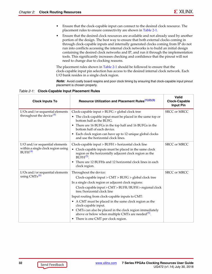
Clock-Capable Input Pin Placement RulesThe two main considerations when manually choosing clock-capable input pins in advance of creating the initial design are:
Send Feedback
32 www.xilinx.com 7 Series FPGAs Clocking Resources User GuideUG472 (v1.14) July 30, 2018
Chapter 2: Clock Routing Resources
• Ensure that the clock-capable input can connect to the desired clock resource. The placement rules to ensure connectivity are shown in Table 2-1.
• Ensure that the desired clock resources are available and not already used by another portion of the design. The best way to ensure that both external clocks coming in through clock-capable inputs and internally generated clocks coming from IP do not run into conflicts accessing the internal clock networks is to build an initial design containing the desired clock networks and IP, and run it through the implementation tools. This significantly increases checking and confidence that the pinout will not need to change due to clocking reasons.
The placement rules shown in Table 2-1 should be followed to ensure that the clock-capable input pin selection has access to the desired internal clock network. Each I/O bank resides in a single clock region.
Note: Avoid costly board respins and poor clock timing by ensuring that clock-capable input pinout placement is chosen properly.
Table 2-1: Clock-Capable Input Placement Rules
Clock Inputs To Resource Utilization and Placement Rules(1)(2) (3)Valid
Clock-Capable Input Pin
I/Os and/or sequential elements throughout the device(4)
Clock-capable input > BUFG > global clock tree
• The clock-capable input must be placed in the same top or bottom half as the BUFG.
• There are 16 BUFGs in the top half and 16 BUFGs in the bottom half of each device.
• Each clock region can have up to 12 unique global clocks and use the horizontal clock lines.
SRCC or MRCC
I/O and/or sequential elements within a single clock region using BUFH(4)
Clock-capable input > BUFH > horizontal clock line
• Clock-capable inputs must be placed in the same clock region or the horizontally adjacent clock region as the BUFH(5).
• There are 12 BUFHs and 12 horizontal clock lines in each clock region.
SRCC or MRCC
I/Os and/or sequential elements using CMTs(6)
Throughout the device:
Clock-capable input > CMT > BUFG > global clock tree
In a single clock region or adjacent clock regions:
Clock-capable input > CMT > BUFR/BUFH > regional clock tree/horizontal clock line
Input routing from clock-capable inputs to CMT:
• A CMT must be placed in the same clock region as the clock-capable input.
• CMTs can also be placed in the clock region immediately above or below when multiple CMTs are needed(5).
• There is one CMT per clock region.
SRCC or MRCC
Send Feedback
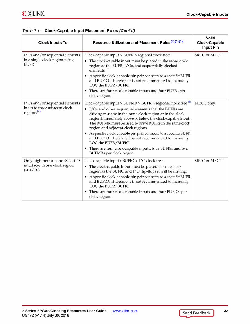
7 Series FPGAs Clocking Resources User Guide www.xilinx.com 33UG472 (v1.14) July 30, 2018
Clock-Capable Inputs
I/Os and/or sequential elements in a single clock region using BUFR
Clock-capable input > BUFR > regional clock tree:
• The clock-capable input must be placed in the same clock region as the BUFR, I/Os, and sequentially clocked elements.
• A specific clock-capable pin pair connects to a specific BUFR and BUFIO. Therefore it is not recommended to manually LOC the BUFR/BUFIO.
• There are four clock-capable inputs and four BUFRs per clock region.
SRCC or MRCC
I/Os and/or sequential elements in up to three adjacent clock regions(7)
Clock-capable input > BUFMR > BUFR > regional clock tree(8)
• I/Os and other sequential elements that the BUFRs are driving must be in the same clock region or in the clock region immediately above or below the clock-capable input. The BUFMR must be used to drive BUFRs in the same clock region and adjacent clock regions.
• A specific clock-capable pin pair connects to a specific BUFR and BUFIO. Therefore it is not recommended to manually LOC the BUFR/BUFIO.
• There are four clock-capable inputs, four BUFRs, and two BUFMRs per clock region.
MRCC only
Only high-performance SelectIO interfaces in one clock region (50 I/Os)
Clock-capable input> BUFIO > I/O clock tree
• The clock-capable input must be placed in same clock region as the BUFIO and I/O flip-flops it will be driving.
• A specific clock-capable pin pair connects to a specific BUFR and BUFIO. Therefore it is not recommended to manually LOC the BUFR/BUFIO.
• There are four clock-capable inputs and four BUFIOs per clock region.
SRCC or MRCC
Table 2-1: Clock-Capable Input Placement Rules (Cont’d)
Clock Inputs To Resource Utilization and Placement Rules(1)(2) (3)Valid
Clock-Capable Input Pin
Send Feedback
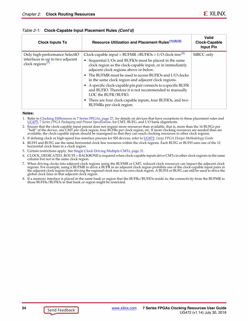
34 www.xilinx.com 7 Series FPGAs Clocking Resources User GuideUG472 (v1.14) July 30, 2018
Chapter 2: Clock Routing Resources
Only high-performance SelectIO interfaces in up to two adjacent clock regions(7)
Clock-capable input > BUFMR >BUFIOs > I/O clock tree(8)
• Sequential I/Os and BUFIOs must be placed in the same clock region as the clock-capable input, or in immediately adjacent clock regions above or below.
• The BUFMR must be used to access BUFIOs and I/O clocks in the same clock region and adjacent clock regions.
• A specific clock-capable pin pair connects to a specific BUFR and BUFIO. Therefore it is not recommended to manually LOC the BUFR/BUFIO.
• There are four clock-capable inputs, four BUFIOs, and two BUFMRs per clock region.
MRCC only
Notes: 1. Refer to Clocking Differences in 7 Series FPGAs, page 27, for details on devices that have exceptions to these placement rules and
UG475, 7 Series FPGA Packaging and Pinout Specification, for CMT, BUFG, and I/O bank alignments.2. Ensure that the clock-capable input pinout does not require more resources than available, that is, more than the 16 BUFGs per
“half” of the device, one CMT per clock region, four BUFRs per clock region, etc. If more clocking resources are needed than are available, the clock-capable inputs should be reassigned so that they can reach clocking resources in other clock regions.
3. If defining clock or high-speed bus interface pinouts for SSI devices, refer to UG872: Large FPGA Design Methodology Guide.4. BUFH and BUFG use the same horizontal clock line resources within the clock regions. Each BUFG or BUFH uses one of the 12
horizontal clock lines in a clock region.5. Certain restrictions apply. See Single Clock Driving Multiple CMTs, page 31.6. CLOCK_DEDICATED_ROUTE = BACKBONE is required when clock-capable inputs drive CMTs in other clock regions in the same
column but not in the same clock region.7. When driving clocks into adjacent clock regions using the BUFMR or CMT, reduced clock resources can impact the adjacent clock
regions. For example, using a BUFMR to drive a BUFR in an adjacent clock region prohibits one of the clock-capable input pairs in the adjacent clock region from driving the regional clock tree in its own clock region. A BUFH or BUFG can still be used to drive the global clock lines in that adjacent clock region.
8. If a memory interface is placed in the same bank or region that the BUFRs/BUFIOs reside in, the connectivity from the BUFMR to those BUFHs/BUFIOs in that bank or region might be restricted.
Table 2-1: Clock-Capable Input Placement Rules (Cont’d)
Clock Inputs To Resource Utilization and Placement Rules(1)(2) (3)Valid
Clock-Capable Input Pin
Send Feedback
7 Series FPGAs Clocking Resources User Guide www.xilinx.com 35UG472 (v1.14) July 30, 2018
Global Clocking Resources
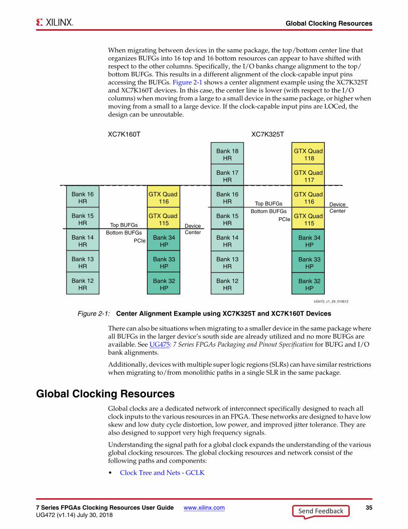
When migrating between devices in the same package, the top/bottom center line that organizes BUFGs into 16 top and 16 bottom resources can appear to have shifted with respect to the other columns. Specifically, the I/O banks change alignment to the top/bottom BUFGs. This results in a different alignment of the clock-capable input pins accessing the BUFGs. Figure 2-1 shows a center alignment example using the XC7K325T and XC7K160T devices. In this case, the center line is lower (with respect to the I/O columns) when moving from a large to a small device in the same package, or higher when moving from a small to a large device. If the clock-capable input pins are LOCed, the design can be unroutable.
There can also be situations when migrating to a smaller device in the same package where all BUFGs in the larger device’s south side are already utilized and no more BUFGs are available. See UG475: 7 Series FPGAs Packaging and Pinout Specification for BUFG and I/O bank alignments.
Additionally, devices with multiple super logic regions (SLRs) can have similar restrictions when migrating to/from monolithic paths in a single SLR in the same package.
Global Clocking ResourcesGlobal clocks are a dedicated network of interconnect specifically designed to reach all clock inputs to the various resources in an FPGA. These networks are designed to have low skew and low duty cycle distortion, low power, and improved jitter tolerance. They are also designed to support very high frequency signals.
Understanding the signal path for a global clock expands the understanding of the various global clocking resources. The global clocking resources and network consist of the following paths and components:
• Clock Tree and Nets - GCLK
X-Ref Target - Figure 2-1
Figure 2-1: Center Alignment Example using XC7K325T and XC7K160T Devices
PCIe
DeviceCenter
Top BUFGsBottom BUFGs
XC7K160T XC7K325T
Bank 18HR
Bank 33HP
Bank 13HR
Bank 34HP
Bank 14HR
Bank 32HP
Bank 12HR
UG472_c1_29_010612
GTX Quad 118
Bank 17HR
GTX Quad 117
Bank 16HR
GTX Quad 116
Bank 15HR
GTX Quad 115
PCIe
DeviceCenter
Top BUFGsBottom BUFGs
Bank 33HP
Bank 13HR
Bank 34HP
Bank 14HR
Bank 32HP
Bank 12HR
Bank 16HR
GTX Quad 116
Bank 15HR
GTX Quad 115
Send Feedback
36 www.xilinx.com 7 Series FPGAs Clocking Resources User GuideUG472 (v1.14) July 30, 2018
Chapter 2: Clock Routing Resources
• Clock Regions
• Global Clock Buffers
Clock Tree and Nets - GCLK7 series FPGAs clock trees are designed for low-skew and low-power operation. Any unused branch is disconnected. The clock trees can also be used to drive logic resources such as reset or clock enable. This is mostly used for high fanout/load nets.
In the 7 series FPGAs architecture, the pin access of the global clock lines are not limited to the logic resources clock pins. The global clock lines can drive pins in the CLB other than CLK pins (for example: the control pins SR and CE). Applications requiring a very fast signal connection and large load/fanout benefit from this architecture.
Clock Regions7 series devices improve the clocking distribution by the use of clock regions. Each clock region can have up to 12 global clock domains. These 12 global clocks can be driven by any combination of the 32 global clock buffers available in a monolithic device or SLR. The dimensions of a clock region are fixed to 50 CLBs tall (50 IOBs) and spanning the left or right side of the die. In 7 series devices, the clock backbone splits the device into a left or right side. The backbone is not located in the center of the die. By fixing the dimensions of the clock region, larger 7 series devices can have more clock regions. The 7 series FPGAs supply from 1 to 24 clock regions.
Global Clock BuffersThere are up to 32 global clock buffers in 7 series devices. A CCIO input can directly connect to any global clock buffer in the same half of the device. Each differential clock pin pair can connect to either a differential or single-ended clock on the PCB. When used as a differential clock input, the direct connection comes from the P-side of the differential input pin pair. When used as a single-ended clock input, the P-side of the pin pair must be used because a direct connection only exists on this pin. For pin naming conventions, refer to the UG475: 7 Series FPGAs Packaging and Pinout Specification. If a single-ended clock is connected to the P-side of a differential pin pair, then the N-side cannot be used as another single-ended clock pin. However, it can be used as a user I/O.
CMTs in the top half of the device can only drive the BUFGs in the top half of the device and CMTs in bottom half can only drive BUFGs in the bottom half. Similarly, only BUFGs in the same half of the device can be used as feedback to the CMTs in the same half of the device. Gigabit transceivers (GTs) can only directly connect to MMCMs/PLLs when the CMT column extends into regions that also contain a full column of GTs and I/Os. The Virtex-7T and Virtex-7XT devices have these full columns. The GTs and CMTs in the Spartan-7, Artix-7, Kintex-7, and Zynq-7000 devices can only be connected using BUFHs (preferred) or BUFGs.
Global clock buffers allow various clock/signal sources to access the global clock trees and nets. The possible sources for input to the global clock buffers include:
• Clock-capable inputs
• Clock management tile (CMT) consisting of mixed-mode clock managers (one MMCM and one PLL per CMT) driving BUFGs in the same half of the device.
• Adjacent global clock buffer outputs (BUFGs)
• General interconnect
Send Feedback
7 Series FPGAs Clocking Resources User Guide www.xilinx.com 37UG472 (v1.14) July 30, 2018
Global Clocking Resources
• Regional clock buffers (BUFRs)
• Gigabit transceivers
The 7 series FPGAs clock-capable inputs can drive global clock buffers indirectly through the vertical clock network that exists in the clock backbone column. The 32 BUFGs are organized into two groups of 16 BUFGs in the top and bottom of the device. Any resources (for example, GTX transceivers) connecting to the BUFGs directly have a top/bottom limitation. For example, each MMCM in the top can only drive the 16 BUFGs residing in that top of the device. Similarly, the MMCMs in the bottom drive the 16 BUFGs in the bottom.
All global clock buffers can drive all clock regions in 7 series devices. However, only 12 different clocks can be driven in a single clock region. A clock region (50 CLBs) is a branch of the clock tree consisting of 25 CLB rows up and 25 CLB rows down. A clock region spans halfway across the device.
The clock buffers are designed to be configured as a synchronous or asynchronous glitch-free 2:1 multiplexer with two clock inputs. There is a dedicated path (routing resource) for BUFG cascading to allow for more than two clock input selections. The 7 series FPGAs control pins provide a wide range of functionality and robust input switching.
In the 7 series FPGAs clocking architecture BUFGCTRL multiplexers and all derivatives can be cascaded to adjacent clock buffers within the group of 16 in the upper and lower half of the device, effectively creating a ring of 16 BUFGMUXes (BUFGCTRL multiplexers) in the upper half and another ring of 16 in the lower half. Figure 2-2 shows a simplified diagram of cascading BUFGs.
The following subsections detail the various configurations, primitives, and use models of the 7 series FPGAs clock buffers.
X-Ref Target - Figure 2-2
Figure 2-2: Cascading BUFGs
UG472_c1_03_091010
Send Feedback
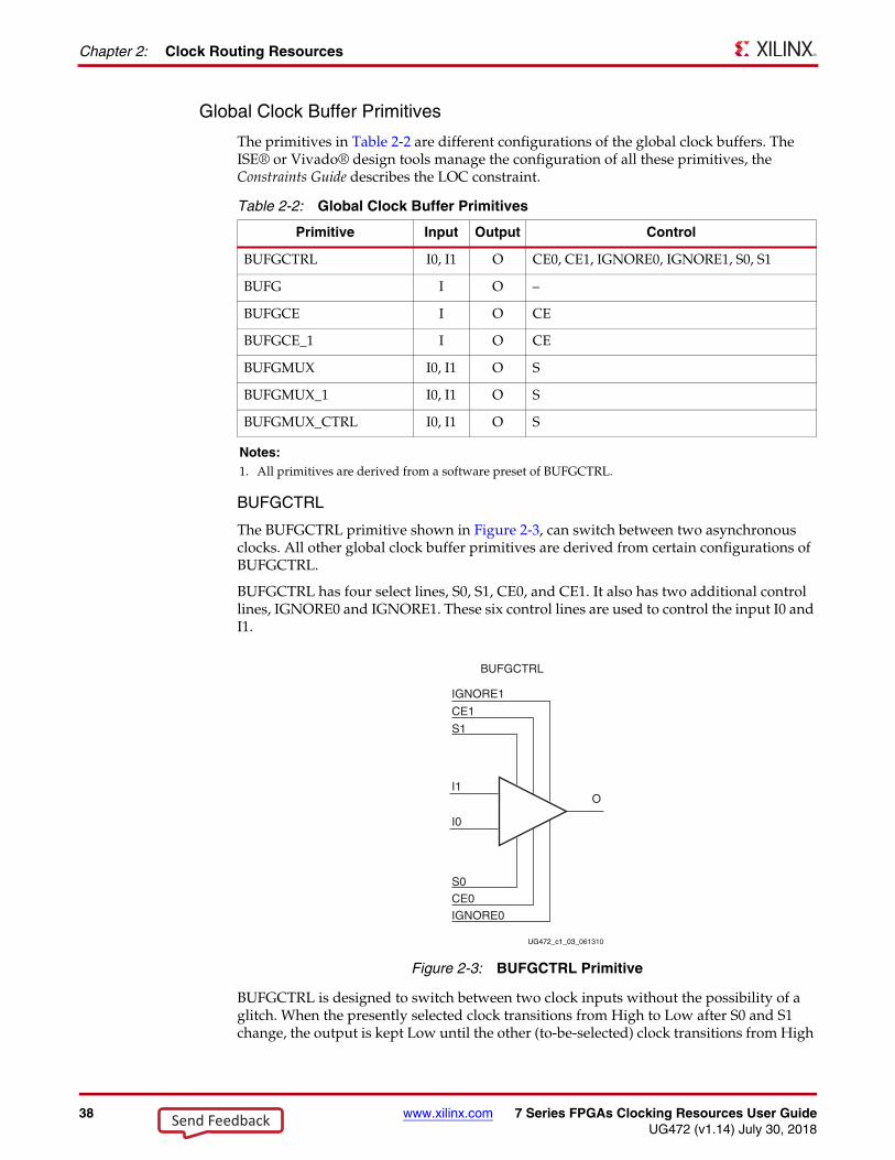
38 www.xilinx.com 7 Series FPGAs Clocking Resources User GuideUG472 (v1.14) July 30, 2018
Chapter 2: Clock Routing Resources
Global Clock Buffer Primitives
The primitives in Table 2-2 are different configurations of the global clock buffers. The ISE® or Vivado® design tools manage the configuration of all these primitives, the Constraints Guide describes the LOC constraint.
BUFGCTRL
The BUFGCTRL primitive shown in Figure 2-3, can switch between two asynchronous clocks. All other global clock buffer primitives are derived from certain configurations of BUFGCTRL.
BUFGCTRL has four select lines, S0, S1, CE0, and CE1. It also has two additional control lines, IGNORE0 and IGNORE1. These six control lines are used to control the input I0 and I1.
BUFGCTRL is designed to switch between two clock inputs without the possibility of a glitch. When the presently selected clock transitions from High to Low after S0 and S1 change, the output is kept Low until the other (to-be-selected) clock transitions from High
Table 2-2: Global Clock Buffer Primitives
Primitive Input Output Control
BUFGCTRL I0, I1 O CE0, CE1, IGNORE0, IGNORE1, S0, S1
BUFG I O –
BUFGCE I O CE
BUFGCE_1 I O CE
BUFGMUX I0, I1 O S
BUFGMUX_1 I0, I1 O S
BUFGMUX_CTRL I0, I1 O S
Notes: 1. All primitives are derived from a software preset of BUFGCTRL.
X-Ref Target - Figure 2-3
Figure 2-3: BUFGCTRL Primitive
IGNORE1
IGNORE0
CE1
CE0
S1
S0
I1
I0
O
BUFGCTRL
UG472_c1_03_061310
Send Feedback
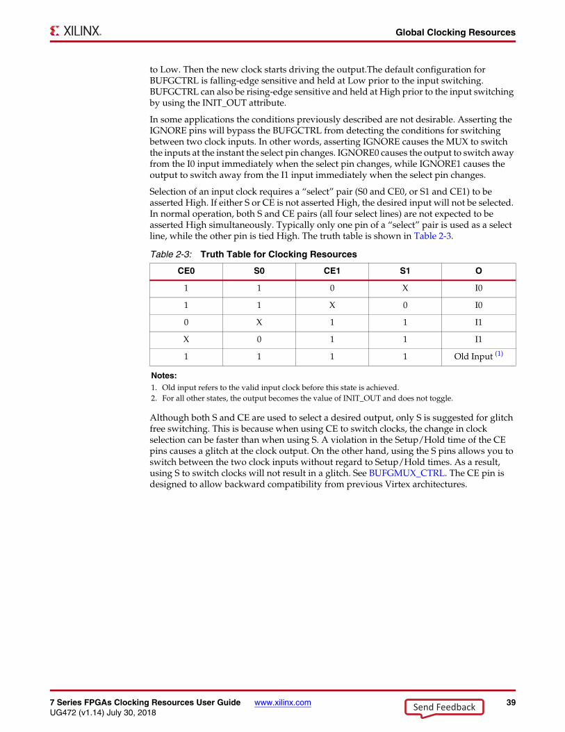
7 Series FPGAs Clocking Resources User Guide www.xilinx.com 39UG472 (v1.14) July 30, 2018
Global Clocking Resources
to Low. Then the new clock starts driving the output.The default configuration for BUFGCTRL is falling-edge sensitive and held at Low prior to the input switching. BUFGCTRL can also be rising-edge sensitive and held at High prior to the input switching by using the INIT_OUT attribute.
In some applications the conditions previously described are not desirable. Asserting the IGNORE pins will bypass the BUFGCTRL from detecting the conditions for switching between two clock inputs. In other words, asserting IGNORE causes the MUX to switch the inputs at the instant the select pin changes. IGNORE0 causes the output to switch away from the I0 input immediately when the select pin changes, while IGNORE1 causes the output to switch away from the I1 input immediately when the select pin changes.
Selection of an input clock requires a “select” pair (S0 and CE0, or S1 and CE1) to be asserted High. If either S or CE is not asserted High, the desired input will not be selected. In normal operation, both S and CE pairs (all four select lines) are not expected to be asserted High simultaneously. Typically only one pin of a “select” pair is used as a select line, while the other pin is tied High. The truth table is shown in Table 2-3.
Although both S and CE are used to select a desired output, only S is suggested for glitch free switching. This is because when using CE to switch clocks, the change in clock selection can be faster than when using S. A violation in the Setup/Hold time of the CE pins causes a glitch at the clock output. On the other hand, using the S pins allows you to switch between the two clock inputs without regard to Setup/Hold times. As a result, using S to switch clocks will not result in a glitch. See BUFGMUX_CTRL. The CE pin is designed to allow backward compatibility from previous Virtex architectures.
Table 2-3: Truth Table for Clocking Resources
CE0 S0 CE1 S1 O
1 1 0 X I0
1 1 X 0 I0
0 X 1 1 I1
X 0 1 1 I1
1 1 1 1 Old Input (1)
Notes: 1. Old input refers to the valid input clock before this state is achieved.2. For all other states, the output becomes the value of INIT_OUT and does not toggle.
Send Feedback
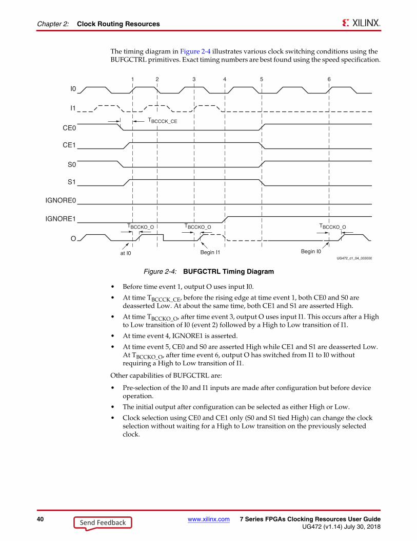
40 www.xilinx.com 7 Series FPGAs Clocking Resources User GuideUG472 (v1.14) July 30, 2018
Chapter 2: Clock Routing Resources
The timing diagram in Figure 2-4 illustrates various clock switching conditions using the BUFGCTRL primitives. Exact timing numbers are best found using the speed specification.
• Before time event 1, output O uses input I0.
• At time TBCCCK_CE, before the rising edge at time event 1, both CE0 and S0 are deasserted Low. At about the same time, both CE1 and S1 are asserted High.
• At time TBCCKO_O, after time event 3, output O uses input I1. This occurs after a High to Low transition of I0 (event 2) followed by a High to Low transition of I1.
• At time event 4, IGNORE1 is asserted.
• At time event 5, CE0 and S0 are asserted High while CE1 and S1 are deasserted Low. At TBCCKO_O, after time event 6, output O has switched from I1 to I0 without requiring a High to Low transition of I1.
Other capabilities of BUFGCTRL are:
• Pre-selection of the I0 and I1 inputs are made after configuration but before device operation.
• The initial output after configuration can be selected as either High or Low.
• Clock selection using CE0 and CE1 only (S0 and S1 tied High) can change the clock selection without waiting for a High to Low transition on the previously selected clock.
X-Ref Target - Figure 2-4
Figure 2-4: BUFGCTRL Timing Diagram
I0
I1
S0
S1
IGNORE0
IGNORE1
O
CE0
CE1
1 2 3 4 5 6
TBCCCK_CE
UG472_c1_04_033030
TBCCKO_O TBCCKO_O TBCCKO_O
at I0 Begin I1 Begin I0
Send Feedback
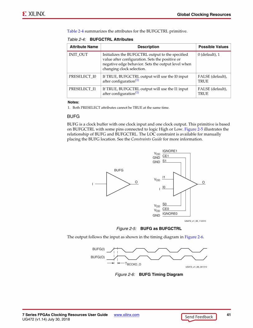
7 Series FPGAs Clocking Resources User Guide www.xilinx.com 41UG472 (v1.14) July 30, 2018
Global Clocking Resources
Table 2-4 summarizes the attributes for the BUFGCTRL primitive.
BUFG
BUFG is a clock buffer with one clock input and one clock output. This primitive is based on BUFGCTRL with some pins connected to logic High or Low. Figure 2-5 illustrates the relationship of BUFG and BUFGCTRL. The LOC constraint is available for manually placing the BUFG location. See the Constraints Guide for more information.
The output follows the input as shown in the timing diagram in Figure 2-6.
Table 2-4: BUFGCTRL Attributes
Attribute Name Description Possible Values
INIT_OUT Initializes the BUFGCTRL output to the specified value after configuration. Sets the positive or negative edge behavior. Sets the output level when changing clock selection.
0 (default), 1
PRESELECT_I0 If TRUE, BUFGCTRL output will use the I0 input after configuration(1)
FALSE (default), TRUE
PRESELECT_I1 If TRUE, BUFGCTRL output will use the I1 input after configuration(1)
FALSE (default), TRUE
Notes: 1. Both PRESELECT attributes cannot be TRUE at the same time.
X-Ref Target - Figure 2-5
Figure 2-5: BUFG as BUFGCTRL
X-Ref Target - Figure 2-6
Figure 2-6: BUFG Timing Diagram
IGNORE1
IGNORE0
CE1
CE0
S1
S0
I1
I0
O
BUFG
UG472_c1_05_112310
VDDGND
VDD
VDD
VDD
I
OI
GND
GND
BUFG(I)
BUFG(O)
TBCCKO_OUG472_c1_06_061310
Send Feedback
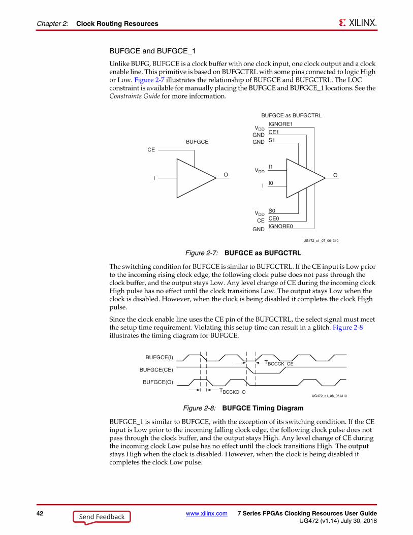
42 www.xilinx.com 7 Series FPGAs Clocking Resources User GuideUG472 (v1.14) July 30, 2018
Chapter 2: Clock Routing Resources
BUFGCE and BUFGCE_1
Unlike BUFG, BUFGCE is a clock buffer with one clock input, one clock output and a clock enable line. This primitive is based on BUFGCTRL with some pins connected to logic High or Low. Figure 2-7 illustrates the relationship of BUFGCE and BUFGCTRL. The LOC constraint is available for manually placing the BUFGCE and BUFGCE_1 locations. See the Constraints Guide for more information.
The switching condition for BUFGCE is similar to BUFGCTRL. If the CE input is Low prior to the incoming rising clock edge, the following clock pulse does not pass through the clock buffer, and the output stays Low. Any level change of CE during the incoming clock High pulse has no effect until the clock transitions Low. The output stays Low when the clock is disabled. However, when the clock is being disabled it completes the clock High pulse.
Since the clock enable line uses the CE pin of the BUFGCTRL, the select signal must meet the setup time requirement. Violating this setup time can result in a glitch. Figure 2-8 illustrates the timing diagram for BUFGCE.
BUFGCE_1 is similar to BUFGCE, with the exception of its switching condition. If the CE input is Low prior to the incoming falling clock edge, the following clock pulse does not pass through the clock buffer, and the output stays High. Any level change of CE during the incoming clock Low pulse has no effect until the clock transitions High. The output stays High when the clock is disabled. However, when the clock is being disabled it completes the clock Low pulse.
X-Ref Target - Figure 2-7
Figure 2-7: BUFGCE as BUFGCTRL
X-Ref Target - Figure 2-8
Figure 2-8: BUFGCE Timing Diagram
IGNORE1
IGNORE0
CE1
CE0
S1
S0
I1
I0
O
BUFGCE
BUFGCE as BUFGCTRL
UG472_c1_07_061310
VDDGND
VDD
CE
VDDO
II
CEGND
GND
BUFGCE(I)
BUFGCE(CE)
BUFGCE(O)
UG472_c1_08_061310TBCCKO_O
TBCCCK_CE
Send Feedback
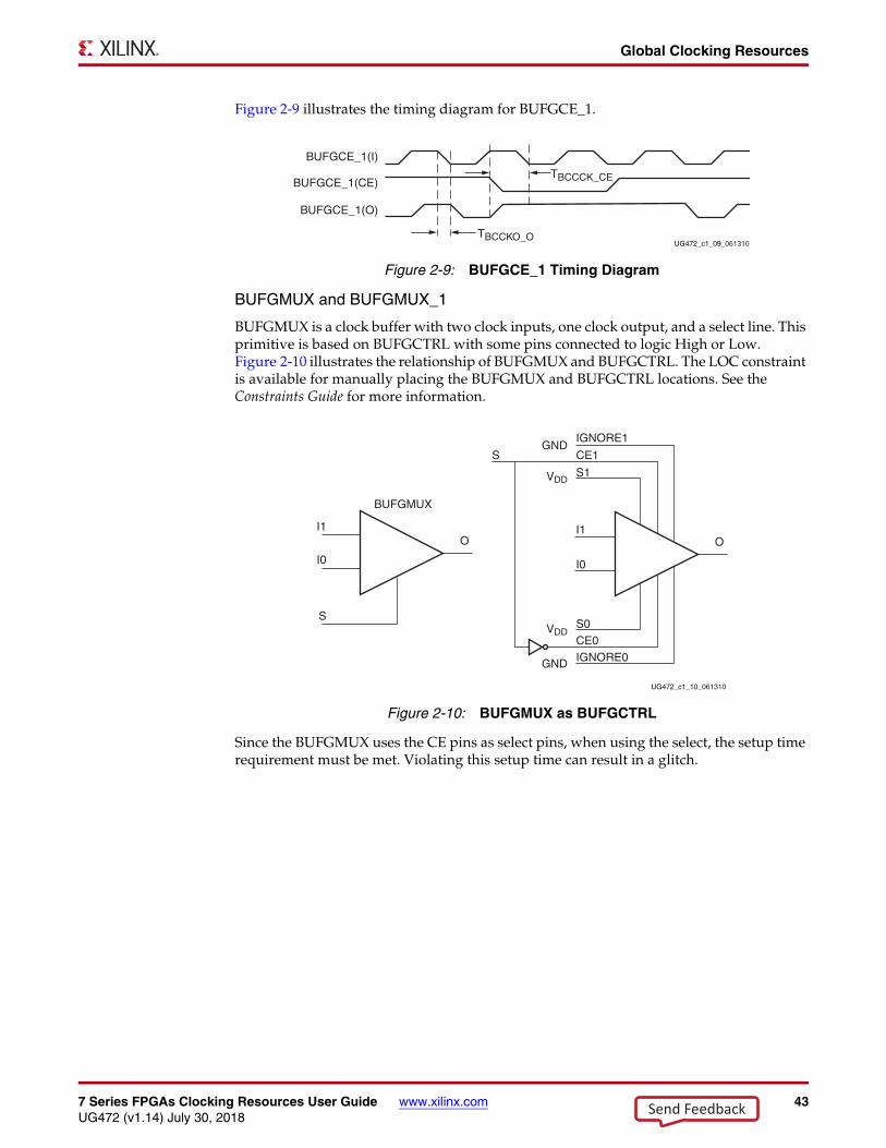
7 Series FPGAs Clocking Resources User Guide www.xilinx.com 43UG472 (v1.14) July 30, 2018
Global Clocking Resources
Figure 2-9 illustrates the timing diagram for BUFGCE_1.
BUFGMUX and BUFGMUX_1
BUFGMUX is a clock buffer with two clock inputs, one clock output, and a select line. This primitive is based on BUFGCTRL with some pins connected to logic High or Low. Figure 2-10 illustrates the relationship of BUFGMUX and BUFGCTRL. The LOC constraint is available for manually placing the BUFGMUX and BUFGCTRL locations. See the Constraints Guide for more information.
Since the BUFGMUX uses the CE pins as select pins, when using the select, the setup time requirement must be met. Violating this setup time can result in a glitch.
X-Ref Target - Figure 2-9
Figure 2-9: BUFGCE_1 Timing Diagram
X-Ref Target - Figure 2-10
Figure 2-10: BUFGMUX as BUFGCTRL
BUFGCE_1(I)
BUFGCE_1(CE)
BUFGCE_1(O)
UG472_c1_09_061310TBCCKO_O
TBCCCK_CE
IGNORE1
IGNORE0
CE1S
CE0
S1
S0
I1
I0
O
BUFGMUX
UG472_c1_10_061310
VDD
VDD
OI1
I0
S
GND
GND
Send Feedback
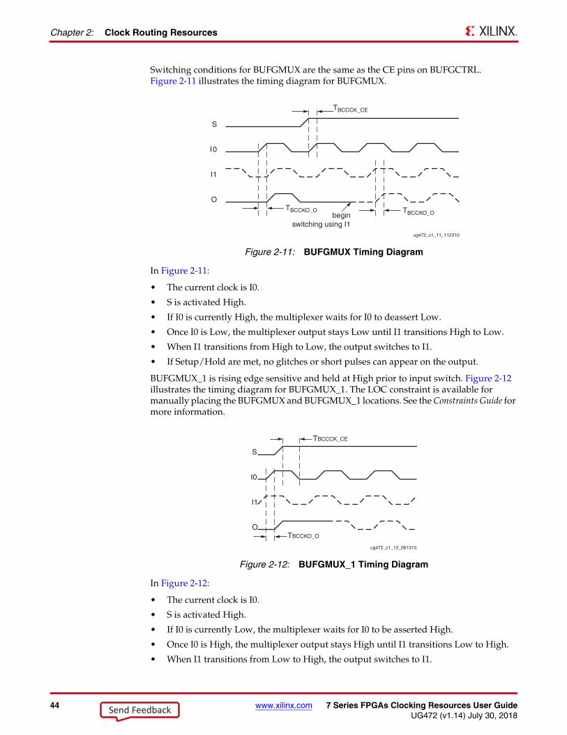
44 www.xilinx.com 7 Series FPGAs Clocking Resources User GuideUG472 (v1.14) July 30, 2018
Chapter 2: Clock Routing Resources
Switching conditions for BUFGMUX are the same as the CE pins on BUFGCTRL. Figure 2-11 illustrates the timing diagram for BUFGMUX.
In Figure 2-11:
• The current clock is I0.
• S is activated High.
• If I0 is currently High, the multiplexer waits for I0 to deassert Low.
• Once I0 is Low, the multiplexer output stays Low until I1 transitions High to Low.
• When I1 transitions from High to Low, the output switches to I1.
• If Setup/Hold are met, no glitches or short pulses can appear on the output.
BUFGMUX_1 is rising edge sensitive and held at High prior to input switch. Figure 2-12 illustrates the timing diagram for BUFGMUX_1. The LOC constraint is available for manually placing the BUFGMUX and BUFGMUX_1 locations. See the Constraints Guide for more information.
In Figure 2-12:
• The current clock is I0.
• S is activated High.
• If I0 is currently Low, the multiplexer waits for I0 to be asserted High.
• Once I0 is High, the multiplexer output stays High until I1 transitions Low to High.
• When I1 transitions from Low to High, the output switches to I1.
X-Ref Target - Figure 2-11
Figure 2-11: BUFGMUX Timing Diagram
X-Ref Target - Figure 2-12
Figure 2-12: BUFGMUX_1 Timing Diagram
S
I0
I1
OTBCCKO_O
ug472_c1_11_112310
TBCCKO_O
TBCCCK_CE
beginswitching using I1
S
I0
I1
O
ug472_c1_12_061310
TBCCCK_CE
TBCCKO_O
Send Feedback
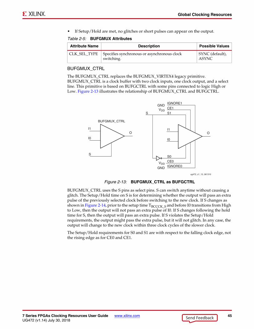
7 Series FPGAs Clocking Resources User Guide www.xilinx.com 45UG472 (v1.14) July 30, 2018
Global Clocking Resources
• If Setup/Hold are met, no glitches or short pulses can appear on the output.
BUFGMUX_CTRL
The BUFGMUX_CTRL replaces the BUFGMUX_VIRTEX4 legacy primitive. BUFGMUX_CTRL is a clock buffer with two clock inputs, one clock output, and a select line. This primitive is based on BUFGCTRL with some pins connected to logic High or Low. Figure 2-13 illustrates the relationship of BUFGMUX_CTRL and BUFGCTRL.
BUFGMUX_CTRL uses the S pins as select pins. S can switch anytime without causing a glitch. The Setup/Hold time on S is for determining whether the output will pass an extra pulse of the previously selected clock before switching to the new clock. If S changes as shown in Figure 2-14, prior to the setup time TBCCCK_S and before I0 transitions from High to Low, then the output will not pass an extra pulse of I0. If S changes following the hold time for S, then the output will pass an extra pulse. If S violates the Setup/Hold requirements, the output might pass the extra pulse, but it will not glitch. In any case, the output will change to the new clock within three clock cycles of the slower clock.
The Setup/Hold requirements for S0 and S1 are with respect to the falling clock edge, not the rising edge as for CE0 and CE1.
Table 2-5: BUFGMUX Attributes
Attribute Name Description Possible Values
CLK_SEL_TYPE Specifies synchronous or asynchronous clock switching.
SYNC (default), ASYNC
X-Ref Target - Figure 2-13
Figure 2-13: BUFGMUX_CTRL as BUFGCTRL
IGNORE1
IGNORE0
CE1
S
CE0
S1
S0
I1
I0
O
BUFGMUX_CTRL
ug472_c1_13_061310
VDD
VDD
OI1
I0
S
GND
GND
Send Feedback
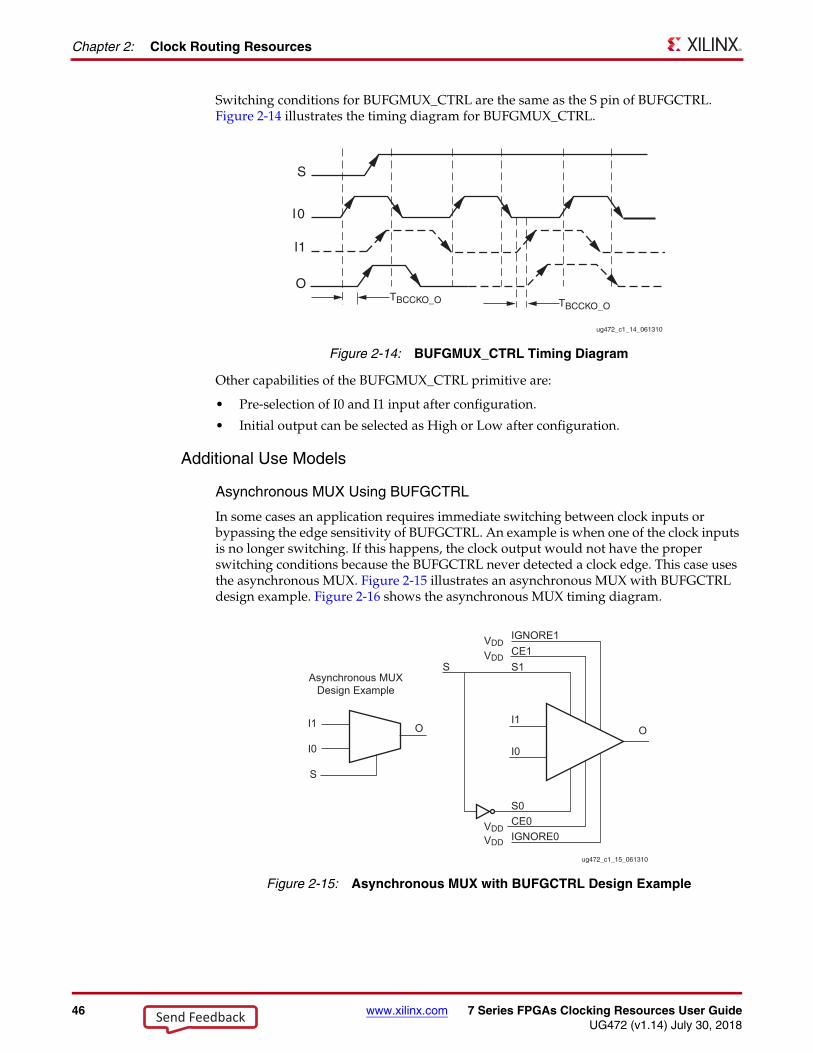
46 www.xilinx.com 7 Series FPGAs Clocking Resources User GuideUG472 (v1.14) July 30, 2018
Chapter 2: Clock Routing Resources
Switching conditions for BUFGMUX_CTRL are the same as the S pin of BUFGCTRL. Figure 2-14 illustrates the timing diagram for BUFGMUX_CTRL.
Other capabilities of the BUFGMUX_CTRL primitive are:
• Pre-selection of I0 and I1 input after configuration.
• Initial output can be selected as High or Low after configuration.
Additional Use Models
Asynchronous MUX Using BUFGCTRL
In some cases an application requires immediate switching between clock inputs or bypassing the edge sensitivity of BUFGCTRL. An example is when one of the clock inputs is no longer switching. If this happens, the clock output would not have the proper switching conditions because the BUFGCTRL never detected a clock edge. This case uses the asynchronous MUX. Figure 2-15 illustrates an asynchronous MUX with BUFGCTRL design example. Figure 2-16 shows the asynchronous MUX timing diagram.
X-Ref Target - Figure 2-14
Figure 2-14: BUFGMUX_CTRL Timing Diagram
S
I0
I1
O
ug472_c1_14_061310
TBCCKO_O TBCCKO_O
X-Ref Target - Figure 2-15
Figure 2-15: Asynchronous MUX with BUFGCTRL Design Example
IGNORE1
IGNORE0
CE1S
CE0
S1
S0
I1
I0
S
I1
I0
O
Asynchronous MUXDesign Example
ug472_c1_15_061310
VDDVDD
VDD
VDD
O
Send Feedback
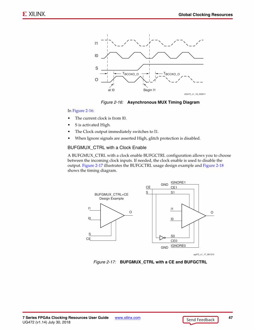
7 Series FPGAs Clocking Resources User Guide www.xilinx.com 47UG472 (v1.14) July 30, 2018
Global Clocking Resources
In Figure 2-16:
• The current clock is from I0.
• S is activated High.
• The Clock output immediately switches to I1.
• When Ignore signals are asserted High, glitch protection is disabled.
BUFGMUX_CTRL with a Clock Enable
A BUFGMUX_CTRL with a clock enable BUFGCTRL configuration allows you to choose between the incoming clock inputs. If needed, the clock enable is used to disable the output. Figure 2-17 illustrates the BUFGCTRL usage design example and Figure 2-18 shows the timing diagram.
X-Ref Target - Figure 2-16
Figure 2-16: Asynchronous MUX Timing Diagram
X-Ref Target - Figure 2-17
Figure 2-17: BUFGMUX_CTRL with a CE and BUFGCTRL
UG472_c1_16_033011
TBCCKO_O TBCCKO_O
I0
I1
S
O
at I0 Begin I1
IGNORE1
IGNORE0
CE1
S
CE
CECE0
S1
S0
I1
I0
O
BUFGMUX_CTRL+CEDesign Example
ug472_c1_17_061310
OI1
I0
S
GND
GND
Send Feedback
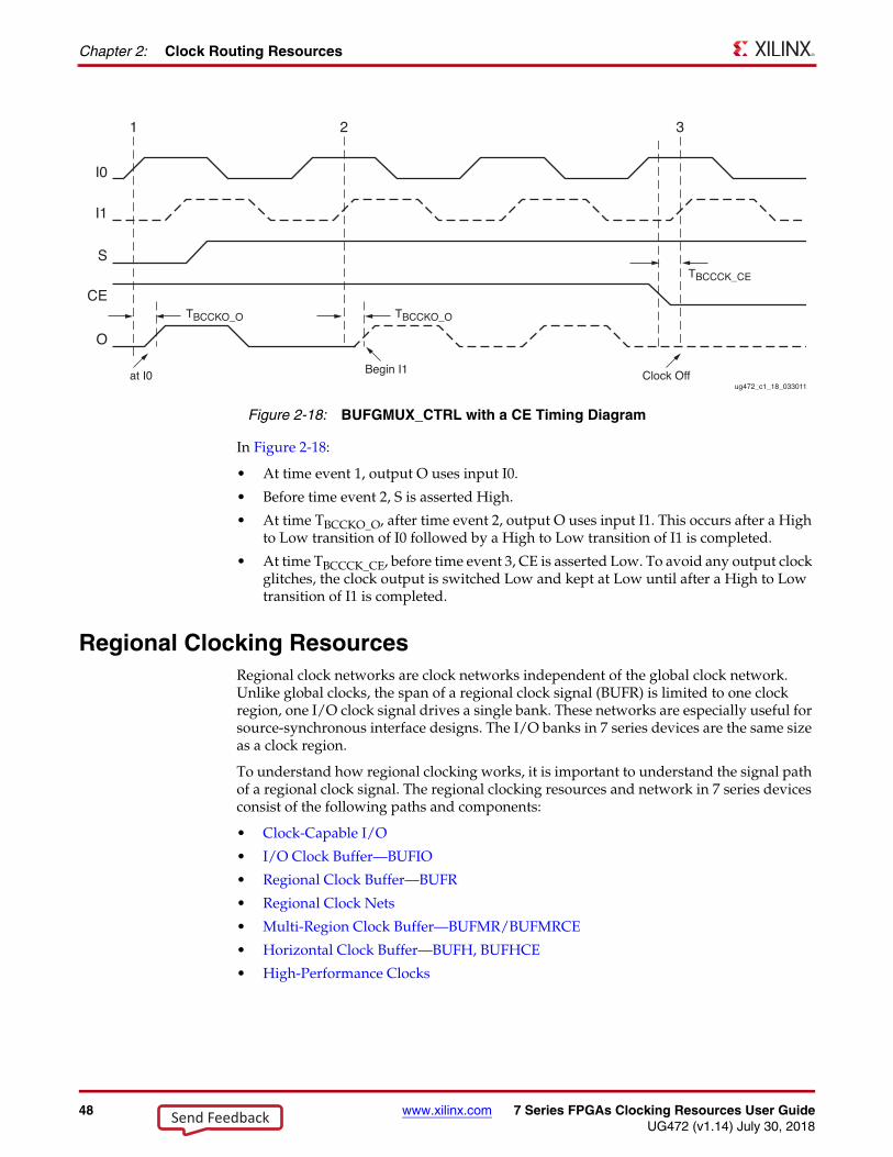
48 www.xilinx.com 7 Series FPGAs Clocking Resources User GuideUG472 (v1.14) July 30, 2018
Chapter 2: Clock Routing Resources
In Figure 2-18:
• At time event 1, output O uses input I0.
• Before time event 2, S is asserted High.
• At time TBCCKO_O, after time event 2, output O uses input I1. This occurs after a High to Low transition of I0 followed by a High to Low transition of I1 is completed.
• At time TBCCCK_CE, before time event 3, CE is asserted Low. To avoid any output clock glitches, the clock output is switched Low and kept at Low until after a High to Low transition of I1 is completed.
Regional Clocking ResourcesRegional clock networks are clock networks independent of the global clock network. Unlike global clocks, the span of a regional clock signal (BUFR) is limited to one clock region, one I/O clock signal drives a single bank. These networks are especially useful for source-synchronous interface designs. The I/O banks in 7 series devices are the same size as a clock region.
To understand how regional clocking works, it is important to understand the signal path of a regional clock signal. The regional clocking resources and network in 7 series devices consist of the following paths and components:
• Clock-Capable I/O
• I/O Clock Buffer—BUFIO
• Regional Clock Buffer—BUFR
• Regional Clock Nets
• Multi-Region Clock Buffer—BUFMR/BUFMRCE
• Horizontal Clock Buffer—BUFH, BUFHCE
• High-Performance Clocks
X-Ref Target - Figure 2-18
Figure 2-18: BUFGMUX_CTRL with a CE Timing Diagram
ug472_c1_18_033011
TBCCKO_O
TBCCCK_CE
TBCCKO_O
at I0 Clock Off
I0
I1
S
CE
O
Begin I1
1 2 3
Send Feedback
7 Series FPGAs Clocking Resources User Guide www.xilinx.com 49UG472 (v1.14) July 30, 2018
Regional Clocking Resources
Clock-Capable I/OEach clock region has four clock-capable I/O pin pairs per I/O bank in every I/O column. Clock-capable I/O pairs are specialized I/O pairs in select locations with special hardware connections to nearby regional clocking resources and other clocking resources. Additionally, clock capable I/O pairs can be used as regular I/O pairs. There are four dedicated clock-capable I/O sites in every bank. When used as clock inputs, clock-capable pins can drive BUFIO, BUFMR, and BUFR. Each I/O column supports regional clock buffers (BUFR). There are two I/O columns in each device.
When used as single-ended clock pins, then as described in Global Clock Buffers the P-side of the pin pair must be used because a direct connection only exists on this pin.
A CCIO can drive any BUFR in the region, but only dedicated CCs can drive specific BUFIOs and MRCCs can drive BUFMRs in a 1:1 relationship. This means that a CCIO has only a single connection to a specific BUFIO or BUFMR.
I/O Clock Buffer—BUFIOThe I/O clock buffer (BUFIO) is a clock buffer available in 7 series devices. The BUFIO drives a dedicated clock net within the I/O bank, independent of the global clocking resources. Thus, BUFIOs are ideally suited for source-synchronous data capture (forwarded/receiver clock distribution). BUFIOs are driven by clock-capable I/Os located in the same bank, by the HPC from the MMCM, or by the BUFMRs in the same and adjacent regions. In a clock region, there are four BUFIOs per bank. Each BUFIO can drive a single I/O clock network in the same region/bank. BUFIOs cannot drive logic resources (CLB, block RAM, DSP, etc.) because the I/O clock network only reaches the I/O column in the same bank/clock region. For multi-region bank support, see Multi-Region Clock Buffer—BUFMR/BUFMRCE.
BUFIOs are driven by:
• SRCCs and MRCCs in the same clock region
• MRCCs in an adjacent clock region using BUFMRs
• MMCMs clock outputs 0-3 driving the HPC in the same clock region
Send Feedback
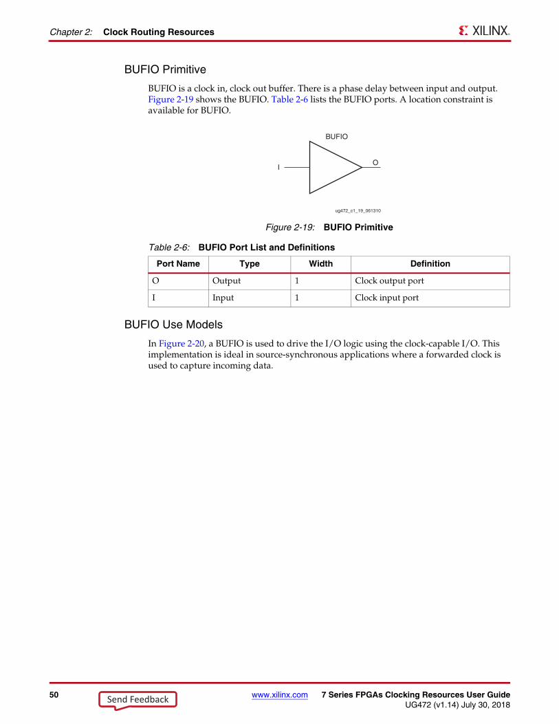
50 www.xilinx.com 7 Series FPGAs Clocking Resources User GuideUG472 (v1.14) July 30, 2018
Chapter 2: Clock Routing Resources
BUFIO Primitive
BUFIO is a clock in, clock out buffer. There is a phase delay between input and output. Figure 2-19 shows the BUFIO. Table 2-6 lists the BUFIO ports. A location constraint is available for BUFIO.
BUFIO Use Models
In Figure 2-20, a BUFIO is used to drive the I/O logic using the clock-capable I/O. This implementation is ideal in source-synchronous applications where a forwarded clock is used to capture incoming data.
X-Ref Target - Figure 2-19
Figure 2-19: BUFIO Primitive
Table 2-6: BUFIO Port List and Definitions
Port Name Type Width Definition
O Output 1 Clock output port
I Input 1 Clock input port
BUFIO
ug472_c1_19_061310
OI
Send Feedback
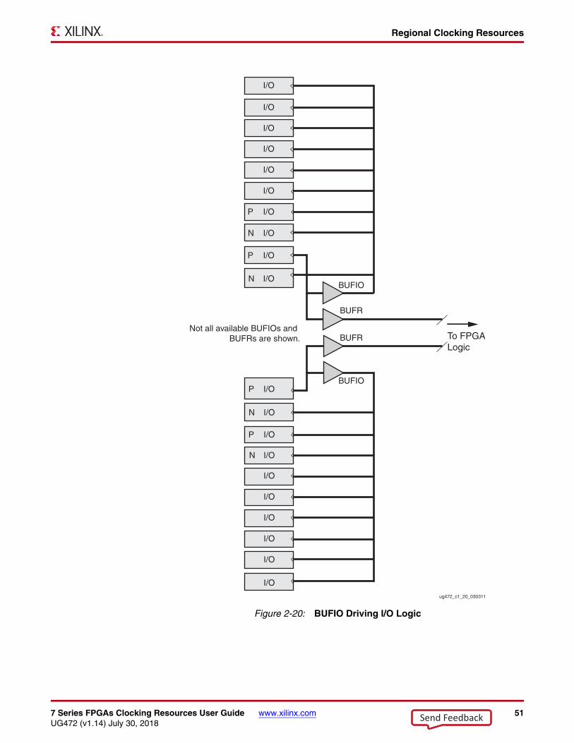
7 Series FPGAs Clocking Resources User Guide www.xilinx.com 51UG472 (v1.14) July 30, 2018
Regional Clocking Resources
X-Ref Target - Figure 2-20
Figure 2-20: BUFIO Driving I/O Logic
I/O
I/O
I/O
I/O
I/O
I/O
I/O
BUFIO
BUFIO
BUFR
BUFR
ug472_c1_20_030311
To FPGALogic
I/O
I/O
I/O
I/O
I/O
I/O
I/O
I/O
I/O
I/O
I/O
I/O
I/O
P
N
P
N
P
N
P
N
Not all available BUFIOs and BUFRs are shown.
Send Feedback
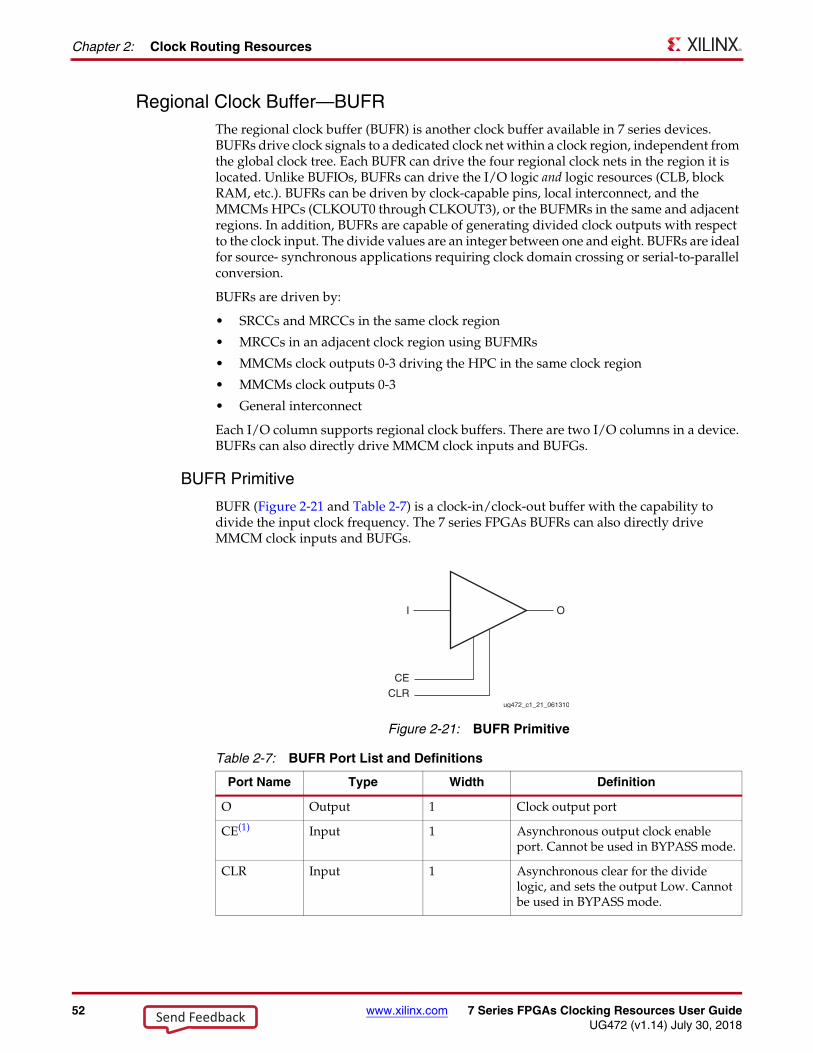
52 www.xilinx.com 7 Series FPGAs Clocking Resources User GuideUG472 (v1.14) July 30, 2018
Chapter 2: Clock Routing Resources
Regional Clock Buffer—BUFRThe regional clock buffer (BUFR) is another clock buffer available in 7 series devices. BUFRs drive clock signals to a dedicated clock net within a clock region, independent from the global clock tree. Each BUFR can drive the four regional clock nets in the region it is located. Unlike BUFIOs, BUFRs can drive the I/O logic and logic resources (CLB, block RAM, etc.). BUFRs can be driven by clock-capable pins, local interconnect, and the MMCMs HPCs (CLKOUT0 through CLKOUT3), or the BUFMRs in the same and adjacent regions. In addition, BUFRs are capable of generating divided clock outputs with respect to the clock input. The divide values are an integer between one and eight. BUFRs are ideal for source- synchronous applications requiring clock domain crossing or serial-to-parallel conversion.
BUFRs are driven by:
• SRCCs and MRCCs in the same clock region
• MRCCs in an adjacent clock region using BUFMRs
• MMCMs clock outputs 0-3 driving the HPC in the same clock region
• MMCMs clock outputs 0-3
• General interconnect
Each I/O column supports regional clock buffers. There are two I/O columns in a device. BUFRs can also directly drive MMCM clock inputs and BUFGs.
BUFR Primitive
BUFR (Figure 2-21 and Table 2-7) is a clock-in/clock-out buffer with the capability to divide the input clock frequency. The 7 series FPGAs BUFRs can also directly drive MMCM clock inputs and BUFGs.X-Ref Target - Figure 2-21
Figure 2-21: BUFR Primitive
Table 2-7: BUFR Port List and Definitions
Port Name Type Width Definition
O Output 1 Clock output port
CE(1) Input 1 Asynchronous output clock enable port. Cannot be used in BYPASS mode.
CLR Input 1 Asynchronous clear for the divide logic, and sets the output Low. Cannot be used in BYPASS mode.
CLRCE
I O
ug472_c1_21_061310
Send Feedback
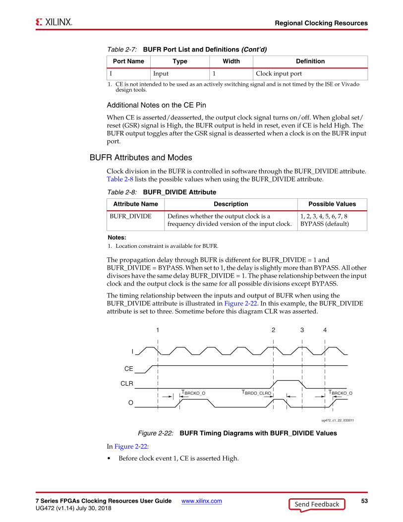
7 Series FPGAs Clocking Resources User Guide www.xilinx.com 53UG472 (v1.14) July 30, 2018
Regional Clocking Resources
Additional Notes on the CE Pin
When CE is asserted/deasserted, the output clock signal turns on/off. When global set/reset (GSR) signal is High, the BUFR output is held in reset, even if CE is held High. The BUFR output toggles after the GSR signal is deasserted when a clock is on the BUFR input port.
BUFR Attributes and Modes
Clock division in the BUFR is controlled in software through the BUFR_DIVIDE attribute. Table 2-8 lists the possible values when using the BUFR_DIVIDE attribute.
The propagation delay through BUFR is different for BUFR_DIVIDE = 1 and BUFR_DIVIDE = BYPASS. When set to 1, the delay is slightly more than BYPASS. All other divisors have the same delay BUFR_DIVIDE = 1. The phase relationship between the input clock and the output clock is the same for all possible divisions except BYPASS.
The timing relationship between the inputs and output of BUFR when using the BUFR_DIVIDE attribute is illustrated in Figure 2-22. In this example, the BUFR_DIVIDE attribute is set to three. Sometime before this diagram CLR was asserted.
In Figure 2-22:
• Before clock event 1, CE is asserted High.
I Input 1 Clock input port
1. CE is not intended to be used as an actively switching signal and is not timed by the ISE or Vivado design tools.
Table 2-7: BUFR Port List and Definitions (Cont’d)
Port Name Type Width Definition
Table 2-8: BUFR_DIVIDE Attribute
Attribute Name Description Possible Values
BUFR_DIVIDE Defines whether the output clock is a frequency divided version of the input clock.
1, 2, 3, 4, 5, 6, 7, 8BYPASS (default)
Notes: 1. Location constraint is available for BUFR.
X-Ref Target - Figure 2-22
Figure 2-22: BUFR Timing Diagrams with BUFR_DIVIDE Values
ug472_c1_22_033011
TBRCKO_O TBRCKO_OTBRDO_CLRO
I
CE
CLR
O
1 2 3 4
Send Feedback
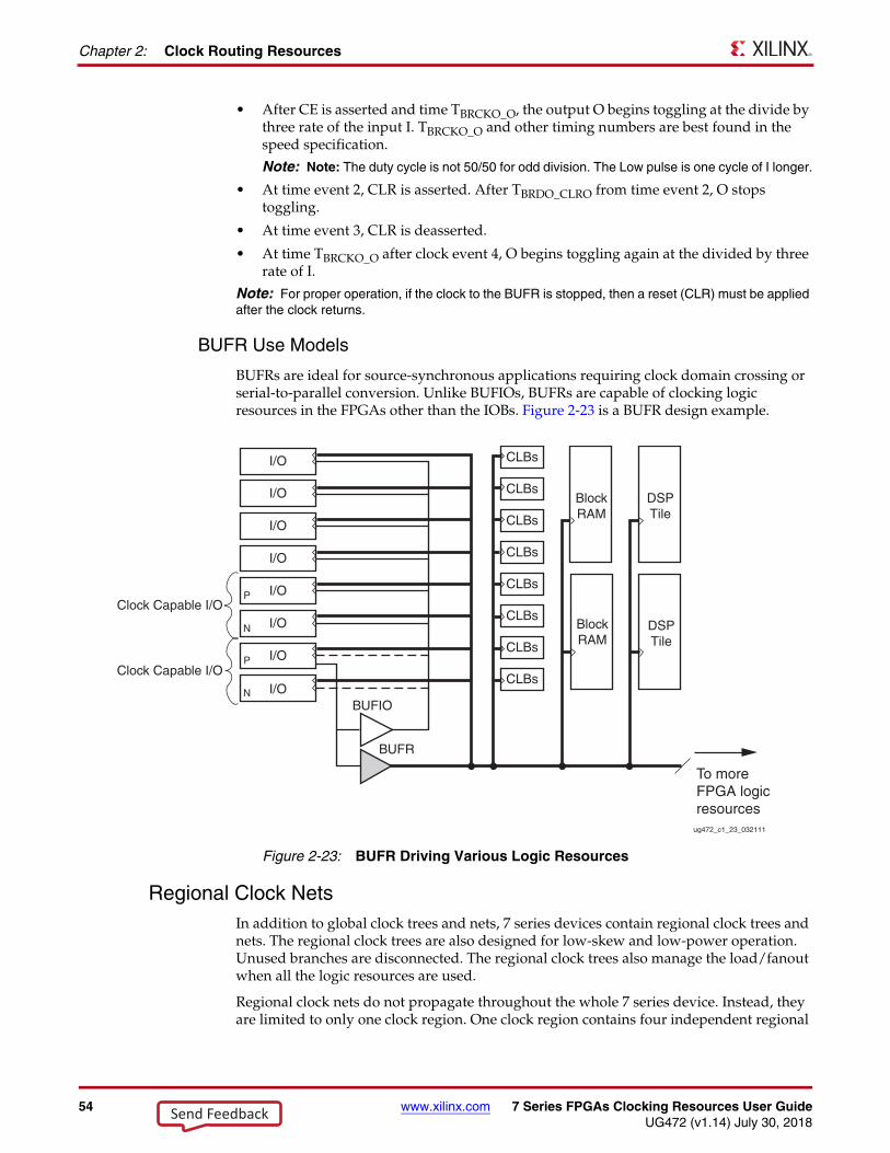
54 www.xilinx.com 7 Series FPGAs Clocking Resources User GuideUG472 (v1.14) July 30, 2018
Chapter 2: Clock Routing Resources
• After CE is asserted and time TBRCKO_O, the output O begins toggling at the divide by three rate of the input I. TBRCKO_O and other timing numbers are best found in the speed specification.
Note: Note: The duty cycle is not 50/50 for odd division. The Low pulse is one cycle of I longer.
• At time event 2, CLR is asserted. After TBRDO_CLRO from time event 2, O stops toggling.
• At time event 3, CLR is deasserted.
• At time TBRCKO_O after clock event 4, O begins toggling again at the divided by three rate of I.
Note: For proper operation, if the clock to the BUFR is stopped, then a reset (CLR) must be applied after the clock returns.
BUFR Use Models
BUFRs are ideal for source-synchronous applications requiring clock domain crossing or serial-to-parallel conversion. Unlike BUFIOs, BUFRs are capable of clocking logic resources in the FPGAs other than the IOBs. Figure 2-23 is a BUFR design example.
Regional Clock NetsIn addition to global clock trees and nets, 7 series devices contain regional clock trees and nets. The regional clock trees are also designed for low-skew and low-power operation. Unused branches are disconnected. The regional clock trees also manage the load/fanout when all the logic resources are used.
Regional clock nets do not propagate throughout the whole 7 series device. Instead, they are limited to only one clock region. One clock region contains four independent regional
X-Ref Target - Figure 2-23
Figure 2-23: BUFR Driving Various Logic Resources
ug472_c1_23_032111
CLBs
CLBs
CLBs
CLBs
CLBs
CLBs
CLBs
CLBs
BlockRAM
BlockRAM
DSPTile
DSPTile
BUFR
To moreFPGA logic resources
I/O
I/O
I/O
I/O
I/O
P
N
P
N
I/O
I/O
I/O
BUFIO
Clock Capable I/O
Clock Capable I/O
Send Feedback
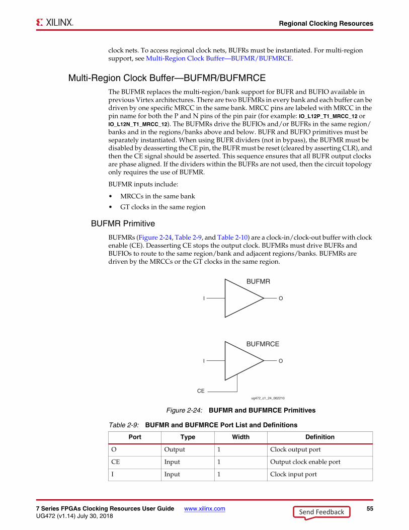
7 Series FPGAs Clocking Resources User Guide www.xilinx.com 55UG472 (v1.14) July 30, 2018
Regional Clocking Resources
clock nets. To access regional clock nets, BUFRs must be instantiated. For multi-region support, see Multi-Region Clock Buffer—BUFMR/BUFMRCE.
Multi-Region Clock Buffer—BUFMR/BUFMRCEThe BUFMR replaces the multi-region/bank support for BUFR and BUFIO available in previous Virtex architectures. There are two BUFMRs in every bank and each buffer can be driven by one specific MRCC in the same bank. MRCC pins are labeled with MRCC in the pin name for both the P and N pins of the pin pair (for example: IO_L12P_T1_MRCC_12 or IO_L12N_T1_MRCC_12). The BUFMRs drive the BUFIOs and/or BUFRs in the same region/banks and in the regions/banks above and below. BUFR and BUFIO primitives must be separately instantiated. When using BUFR dividers (not in bypass), the BUFMR must be disabled by deasserting the CE pin, the BUFR must be reset (cleared by asserting CLR), and then the CE signal should be asserted. This sequence ensures that all BUFR output clocks are phase aligned. If the dividers within the BUFRs are not used, then the circuit topology only requires the use of BUFMR.
BUFMR inputs include:
• MRCCs in the same bank
• GT clocks in the same region
BUFMR Primitive
BUFMRs (Figure 2-24, Table 2-9, and Table 2-10) are a clock-in/clock-out buffer with clock enable (CE). Deasserting CE stops the output clock. BUFMRs must drive BUFRs and BUFIOs to route to the same region/bank and adjacent regions/banks. BUFMRs are driven by the MRCCs or the GT clocks in the same region.X-Ref Target - Figure 2-24
Figure 2-24: BUFMR and BUFMRCE Primitives
Table 2-9: BUFMR and BUFMRCE Port List and Definitions
Port Type Width Definition
O Output 1 Clock output port
CE Input 1 Output clock enable port
I Input 1 Clock input port
I O
BUFMR
ug472_c1_24_062210
CE
I O
BUFMRCE
Send Feedback
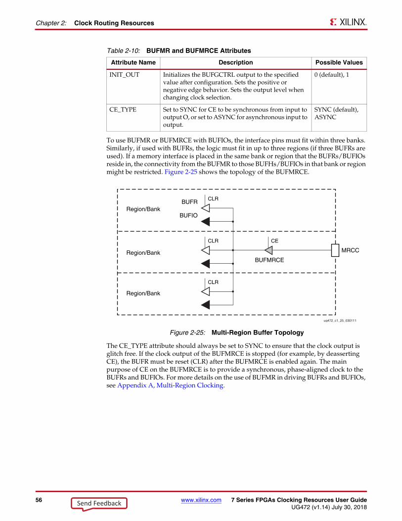
56 www.xilinx.com 7 Series FPGAs Clocking Resources User GuideUG472 (v1.14) July 30, 2018
Chapter 2: Clock Routing Resources
To use BUFMR or BUFMRCE with BUFIOs, the interface pins must fit within three banks. Similarly, if used with BUFRs, the logic must fit in up to three regions (if three BUFRs are used). If a memory interface is placed in the same bank or region that the BUFRs/BUFIOs reside in, the connectivity from the BUFMR to those BUFHs/BUFIOs in that bank or region might be restricted. Figure 2-25 shows the topology of the BUFMRCE.
The CE_TYPE attribute should always be set to SYNC to ensure that the clock output is glitch free. If the clock output of the BUFMRCE is stopped (for example, by deasserting CE), the BUFR must be reset (CLR) after the BUFMRCE is enabled again. The main purpose of CE on the BUFMRCE is to provide a synchronous, phase-aligned clock to the BUFRs and BUFIOs. For more details on the use of BUFMR in driving BUFRs and BUFIOs, see Appendix A, Multi-Region Clocking.
Table 2-10: BUFMR and BUFMRCE Attributes
Attribute Name Description Possible Values
INIT_OUT Initializes the BUFGCTRL output to the specified value after configuration. Sets the positive or negative edge behavior. Sets the output level when changing clock selection.
0 (default), 1
CE_TYPE Set to SYNC for CE to be synchronous from input to output O, or set to ASYNC for asynchronous input to output.
SYNC (default), ASYNC
X-Ref Target - Figure 2-25
Figure 2-25: Multi-Region Buffer Topology
CLRBUFR
BUFMRCE
BUFIORegion/Bank
Region/Bank MRCC
Region/Bank
ug472_c1_25_030111
CLR CE
CLR
Send Feedback
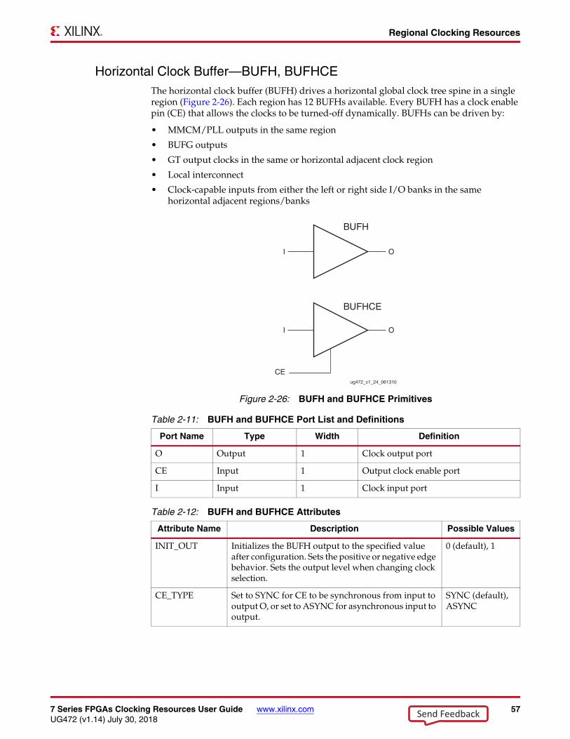
7 Series FPGAs Clocking Resources User Guide www.xilinx.com 57UG472 (v1.14) July 30, 2018
Regional Clocking Resources
Horizontal Clock Buffer—BUFH, BUFHCEThe horizontal clock buffer (BUFH) drives a horizontal global clock tree spine in a single region (Figure 2-26). Each region has 12 BUFHs available. Every BUFH has a clock enable pin (CE) that allows the clocks to be turned-off dynamically. BUFHs can be driven by:
• MMCM/PLL outputs in the same region
• BUFG outputs
• GT output clocks in the same or horizontal adjacent clock region
• Local interconnect
• Clock-capable inputs from either the left or right side I/O banks in the same horizontal adjacent regions/banks
X-Ref Target - Figure 2-26
Figure 2-26: BUFH and BUFHCE Primitives
Table 2-11: BUFH and BUFHCE Port List and Definitions
Port Name Type Width Definition
O Output 1 Clock output port
CE Input 1 Output clock enable port
I Input 1 Clock input port
Table 2-12: BUFH and BUFHCE Attributes
Attribute Name Description Possible Values
INIT_OUT Initializes the BUFH output to the specified value after configuration. Sets the positive or negative edge behavior. Sets the output level when changing clock selection.
0 (default), 1
CE_TYPE Set to SYNC for CE to be synchronous from input to output O, or set to ASYNC for asynchronous input to output.
SYNC (default), ASYNC
I O
ug472_c1_24_061310
CE
I O
BUFH
BUFHCE
Send Feedback
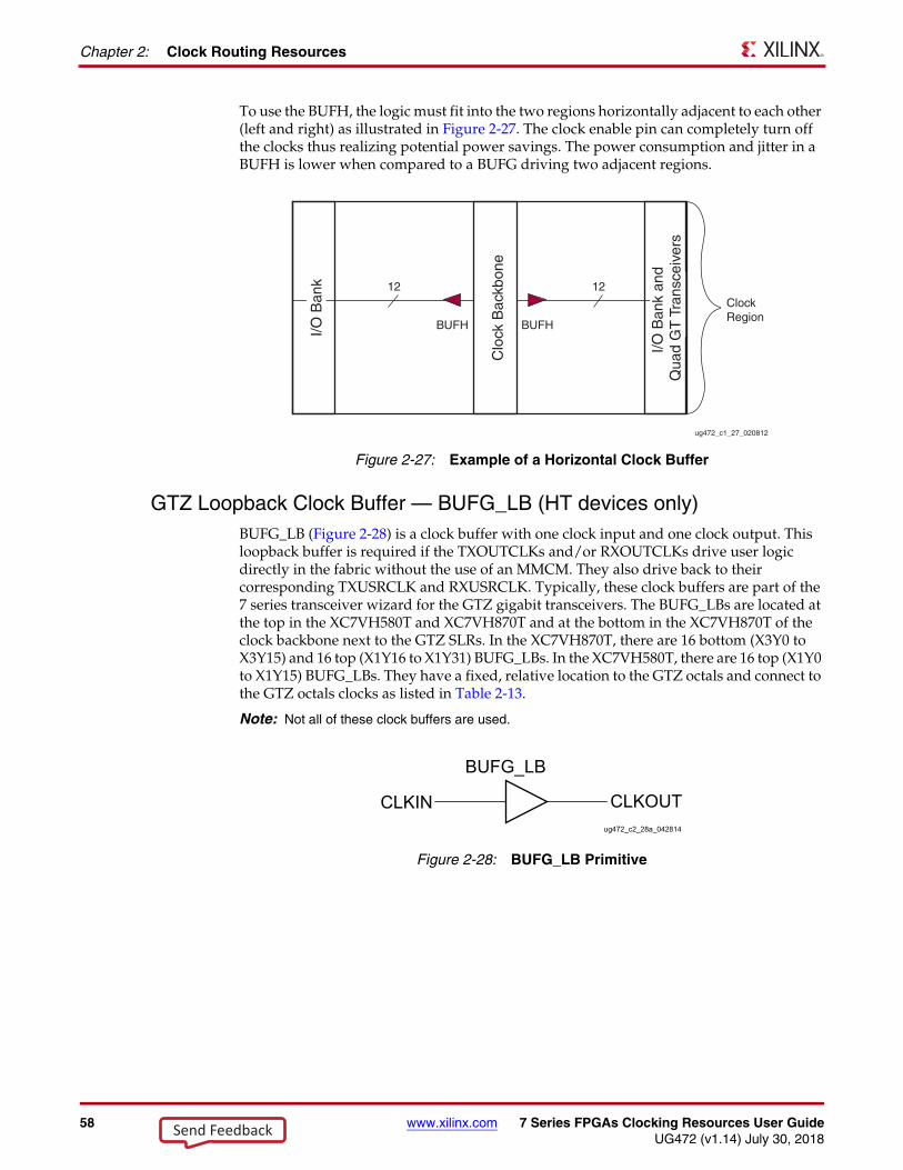
58 www.xilinx.com 7 Series FPGAs Clocking Resources User GuideUG472 (v1.14) July 30, 2018
Chapter 2: Clock Routing Resources
To use the BUFH, the logic must fit into the two regions horizontally adjacent to each other (left and right) as illustrated in Figure 2-27. The clock enable pin can completely turn off the clocks thus realizing potential power savings. The power consumption and jitter in a BUFH is lower when compared to a BUFG driving two adjacent regions.
GTZ Loopback Clock Buffer — BUFG_LB (HT devices only)BUFG_LB (Figure 2-28) is a clock buffer with one clock input and one clock output. This loopback buffer is required if the TXOUTCLKs and/or RXOUTCLKs drive user logic directly in the fabric without the use of an MMCM. They also drive back to their corresponding TXUSRCLK and RXUSRCLK. Typically, these clock buffers are part of the 7 series transceiver wizard for the GTZ gigabit transceivers. The BUFG_LBs are located at the top in the XC7VH580T and XC7VH870T and at the bottom in the XC7VH870T of the clock backbone next to the GTZ SLRs. In the XC7VH870T, there are 16 bottom (X3Y0 to X3Y15) and 16 top (X1Y16 to X1Y31) BUFG_LBs. In the XC7VH580T, there are 16 top (X1Y0 to X1Y15) BUFG_LBs. They have a fixed, relative location to the GTZ octals and connect to the GTZ octals clocks as listed in Table 2-13.
Note: Not all of these clock buffers are used.
X-Ref Target - Figure 2-27
Figure 2-27: Example of a Horizontal Clock Buffer
ug472_c1_27_020812
Clo
ck B
ackb
one
BUFH BUFH
ClockRegion
12 12
I/O B
ank
I/O B
ank
and
Qua
d G
T T
rans
ceiv
ers
X-Ref Target - Figure 2-28
Figure 2-28: BUFG_LB Primitive
CLKOUTCLKIN
BUFG_LB
ug472_c2_28a_042814
Send Feedback
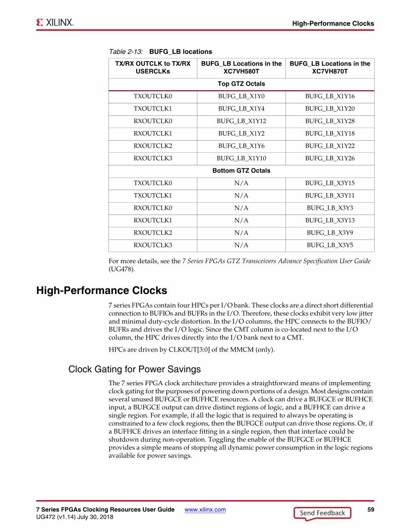
7 Series FPGAs Clocking Resources User Guide www.xilinx.com 59UG472 (v1.14) July 30, 2018
High-Performance Clocks
For more details, see the 7 Series FPGAs GTZ Transceivers Advance Specification User Guide (UG478).
High-Performance Clocks7 series FPGAs contain four HPCs per I/O bank. These clocks are a direct short differential connection to BUFIOs and BUFRs in the I/O. Therefore, these clocks exhibit very low jitter and minimal duty-cycle distortion. In the I/O columns, the HPC connects to the BUFIO/BUFRs and drives the I/O logic. Since the CMT column is co-located next to the I/O column, the HPC drives directly into the I/O bank next to a CMT.
HPCs are driven by CLKOUT[3:0] of the MMCM (only).
Clock Gating for Power SavingsThe 7 series FPGA clock architecture provides a straightforward means of implementing clock gating for the purposes of powering down portions of a design. Most designs contain several unused BUFGCE or BUFHCE resources. A clock can drive a BUFGCE or BUFHCE input, a BUFGCE output can drive distinct regions of logic, and a BUFHCE can drive a single region. For example, if all the logic that is required to always be operating is constrained to a few clock regions, then the BUFGCE output can drive those regions. Or, if a BUFHCE drives an interface fitting in a single region, then that interface could be shutdown during non-operation. Toggling the enable of the BUFGCE or BUFHCE provides a simple means of stopping all dynamic power consumption in the logic regions available for power savings.
Table 2-13: BUFG_LB locations
TX/RX OUTCLK to TX/RX USERCLKs
BUFG_LB Locations in the XC7VH580T
BUFG_LB Locations in the XC7VH870T
Top GTZ Octals
TXOUTCLK0 BUFG_LB_X1Y0 BUFG_LB_X1Y16
TXOUTCLK1 BUFG_LB_X1Y4 BUFG_LB_X1Y20
RXOUTCLK0 BUFG_LB_X1Y12 BUFG_LB_X1Y28
RXOUTCLK1 BUFG_LB_X1Y2 BUFG_LB_X1Y18
RXOUTCLK2 BUFG_LB_X1Y6 BUFG_LB_X1Y22
RXOUTCLK3 BUFG_LB_X1Y10 BUFG_LB_X1Y26
Bottom GTZ Octals
TXOUTCLK0 N/A BUFG_LB_X3Y15
TXOUTCLK1 N/A BUFG_LB_X3Y11
RXOUTCLK0 N/A BUFG_LB_X3Y3
RXOUTCLK1 N/A BUFG_LB_X3Y13
RXOUTCLK2 N/A BUFG_LB_X3Y9
RXOUTCLK3 N/A BUFG_LB_X3Y5
Send Feedback
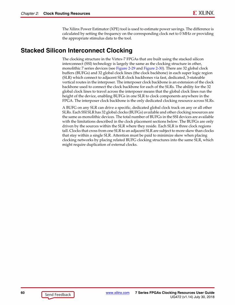
60 www.xilinx.com 7 Series FPGAs Clocking Resources User GuideUG472 (v1.14) July 30, 2018
Chapter 2: Clock Routing Resources
The Xilinx Power Estimator (XPE) tool is used to estimate power savings. The difference is calculated by setting the frequency on the corresponding clock net to 0 MHz or providing the appropriate stimulus data to the tool.
Stacked Silicon Interconnect ClockingThe clocking structure in the Virtex-7 FPGAs that are built using the stacked silicon interconnect (SSI) technology is largely the same as the clocking structure in other, monolithic 7 series devices (see Figure 2-29 and Figure 2-30). There are 32 global clock buffers (BUFGs) and 32 global clock lines (the clock backbone) in each super logic region (SLR) which connect to adjacent SLR clock backbones via fast, dedicated, 3-stateable vertical routes in the interposer. The interposer clock backbone is an extension of the clock backbone used to connect the clock backbone for each of the SLRs. The ability for the 32 global clock lines to travel across the interposer means that the global clock lines run the height of the device, enabling BUFGs in one SLR to clock components anywhere in the FPGA. The interposer clock backbone is the only dedicated clocking resource across SLRs.
A BUFG on any SLR can drive a specific, dedicated global clock track on any or all other SLRs. Each SSI SLR has 32 global clocks (BUFGs) available and other clocking resources are the same as monolithic devices. The total number of BUFGs in the SSI devices are available with the limitations described in the clock placement sections below. The BUFGs are only driven by the sources within the SLR where they reside. Each SLR is three clock regions tall. Clocks that cross from one SLR to an adjacent SLR are subject to more skew than clocks that stay within a single SLR. Attention must be paid to minimize skew when placing clocking networks by placing related BUFG clocking structures into the same SLR, which might require duplication of external clocks.
Send Feedback
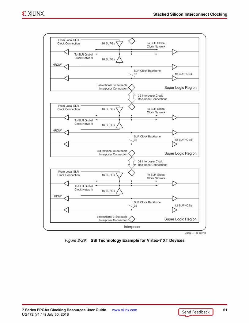
7 Series FPGAs Clocking Resources User Guide www.xilinx.com 61UG472 (v1.14) July 30, 2018
Stacked Silicon Interconnect Clocking
X-Ref Target - Figure 2-29
Figure 2-29: SSI Technology Example for Virtex-7 XT Devices
Super Logic Region
To SLR GlobalClock Network
Bidirectional 3-StateableInterposer Connection
SLR Clock Backbone32
32 Interposer ClockBackbone Connections
To SLR GlobalClock Network
HROW
12 BUFHCEs
16 BUFGs
16 BUFGs
From Local SLRClock Connection
Super Logic Region
To SLR GlobalClock Network
Bidirectional 3 StateableInterposer Connection
SLR Clock Backbone32
32 Interposer ClockBackbone Connections
To SLR GlobalClock Network
HROW
12 BUFHCEs
16 BUFGs
16 BUFGs
From Local SLRClock Connection
Super Logic Region
UG472_c1_28_020712
Interposer
To SLR GlobalClock Network
Bidirectional 3-StateableInterposer Connection
SLR Clock Backbone32
To SLR GlobalClock Network
HROW
12 BUFHCEs
16 BUFGs
16 BUFGs
From Local SLRClock Connection
Send Feedback
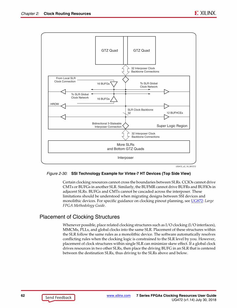
62 www.xilinx.com 7 Series FPGAs Clocking Resources User GuideUG472 (v1.14) July 30, 2018
Chapter 2: Clock Routing Resources
Certain clocking resources cannot cross the boundaries between SLRs. CCIOs cannot drive CMTs or BUFGs in another SLR. Similarly, the BUFMR cannot drive BUFRs and BUFIOs in adjacent SLRs. BUFGs and CMTs cannot be cascaded across the interposer. These limitations should be understood when migrating designs between SSI devices and monolithic devices. For specific guidance on clocking pinout planning, see UG872: Large FPGA Methodology Guide.
Placement of Clocking StructuresWhenever possible, place related clocking structures such as I/O clocking (I/O interfaces), MMCMs, PLLs, and global clocks into the same SLR. Placement of these structures within the SLR follow the same rules as a monolithic device. The software automatically resolves conflicting rules when the clocking logic is constrained to the SLR level by you. However, placement of clock structures within single SLR can minimize skew effect. If a global clock drives resources in two other SLRs, then place the driving BUFG in an SLR that is centered between the destination SLRs, thus driving to the SLRs above and below.
X-Ref Target - Figure 2-30
Figure 2-30: SSI Technology Example for Virtex-7 HT Devices (Top Side View)
Super Logic Region
To SLR GlobalClock Network
Bidirectional 3-StateableInterposer Connection
SLR Clock Backbone32
32 Interposer ClockBackbone Connections
To SLR GlobalClock Network
HROW
12 BUFHCEs
16 BUFGs
16 BUFGs
From Local SLRClock Connection
32 Interposer ClockBackbone Connections
More SLRsand Bottom GTZ Quads
GTZ Quad GTZ Quad
UG472_c2_19_061212
Interposer
Send Feedback
7 Series FPGAs Clocking Resources User Guide www.xilinx.com 63UG472 (v1.14) July 30, 2018
Stacked Silicon Interconnect Clocking
Clock Buffer PlacementA single global clock buffer can drive any clocking point in any SLR. The global clock buffers are competing for the 32 available interposer clock backbone tracks. A track driven by a BUFG in one SLR cannot be driven by another BUFG in the same or any other SLR. Because each SLR clock track is segmentable at the SLR boundary, a BUFG in one SLR can use the same track as a BUFG in an adjacent SLR as long as the clocking is local to the SLR and does not need to connect to an adjacent SLR.
For example, in the largest SSI device (XC7V2000T), each of the SLRs has 32 BUFGs. The BUFGs and the associated clock nets can be viewed as four groups of 0–31, 32–63, 64–95, and 96–127 from the bottom SLR up to the top. BUFGs and clock nets that are multiples of 32 (32 indices apart from each other) contend for the same interposer backbone resources. In this XC7V2000T example, these are SLR clock nets 0, 32, 64, and 96; 1, 33, 65, and 97; and so on. With four SLRs, the BUFGs X0Y0, X0Y32, X0Y64, and X0Y96 (all called BUFG0s in Figure 2-31) connect to the same track 0 in the interposer backbone. Therefore, only one of those buffers can be used in the design. Similarly, the BUFGs X0Y1, X0Y33, X0Y65, and X0Y97 (all BUFG1s) compete for interposer backbone track 1.
Send Feedback
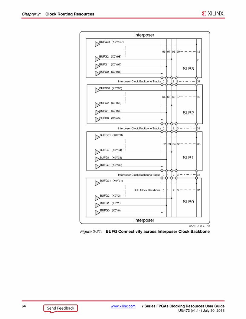
64 www.xilinx.com 7 Series FPGAs Clocking Resources User GuideUG472 (v1.14) July 30, 2018
Chapter 2: Clock Routing Resources
X-Ref Target - Figure 2-31
Figure 2-31: BUFG Connectivity across Interposer Clock Backbone
Interposer
Interposer Clock Backbone tracks 31
BUFG0 (X0Y0)
BUFG1 (X0Y1)
BUFG2 (X0Y2)
BUFG31 (X0Y31)
SLR0
0 1 3 31 2
0 1 3 2
BUFG0 (X0Y32)
BUFG1 (X0Y33)
BUFG2 (X0Y34)
BUFG31 (X0Y63)
SLR1
31 0 1 3 2
31 0 1 3 2
SLR Clock Backbone
BUFG0 (X0Y64)
BUFG1 (X0Y65)
BUFG2 (X0Y66)
SLR2
BUFG0 (X0Y96)
BUFG1 (X0Y97)
BUFG2 (X0Y98)
SLR3
BUFG31 (X0Y95)
BUFG31 (X0Y127)
UG472_c2_18_011712
63 32 33 35 34
95 64 65 67 66
12
7
96 97 99 98
Interposer Clock Backbone Tracks
Interposer Clock Backbone Tracks
Interposer
Send Feedback
7 Series FPGAs Clocking Resources User Guide www.xilinx.com 65UG472 (v1.14) July 30, 2018
Chapter 3
Clock Management Tile
IntroductionIn 7 series FPGAs, the clock management tile (CMT) includes a mixed-mode clock manager (MMCM) and a phase-locked loop (PLL). The PLL contains a subset of the MMCM functions. At the core of the 7 series FPGAs CMT is the architecture similar to the Virtex-5 and Virtex-6 FPGAs with enhanced functions and capabilities. The CMT backbone can be used to chain CMT clocking functions; however, there are limitations to placement, distance, and connectivity resources. See Appendix B, Clocking Resources and Connectivity Variations per Clock Region.
The CMT diagram (Figure 3-1) shows a high-level view of the connection between the various clock input sources and the MMCM/PLL. In 7 series FPGAs, the clock input connectivity allows multiple resources to provide the reference clock(s) to the MMCM/PLL. The number of output counters (dividers) is eight with some of them capable of driving out an inverted clock signal (180° phase shift). For backward compatibility with DCMs, nine independent outputs can be selected for mapping the DCM outputs directly into the MMCM. 7 series FPGAs MMCMs have infinite fine phase-shift capability in either direction and can be used in dynamic phase-shift mode. The resolution of the fine phase shift depends on the VCO frequency. Fractional divide functionality in increments of 1/8th (0.125) for CLKFBOUT and CLKOUT0 are available to support greater clock frequency synthesis capability. 7 series FPGAs have added spread spectrum capabilities to the MMCMs. If the MMCM spread spectrum feature is not used, a spread spectrum on an external input clock will not be filtered and thus passed on to the output clock.
Send Feedback
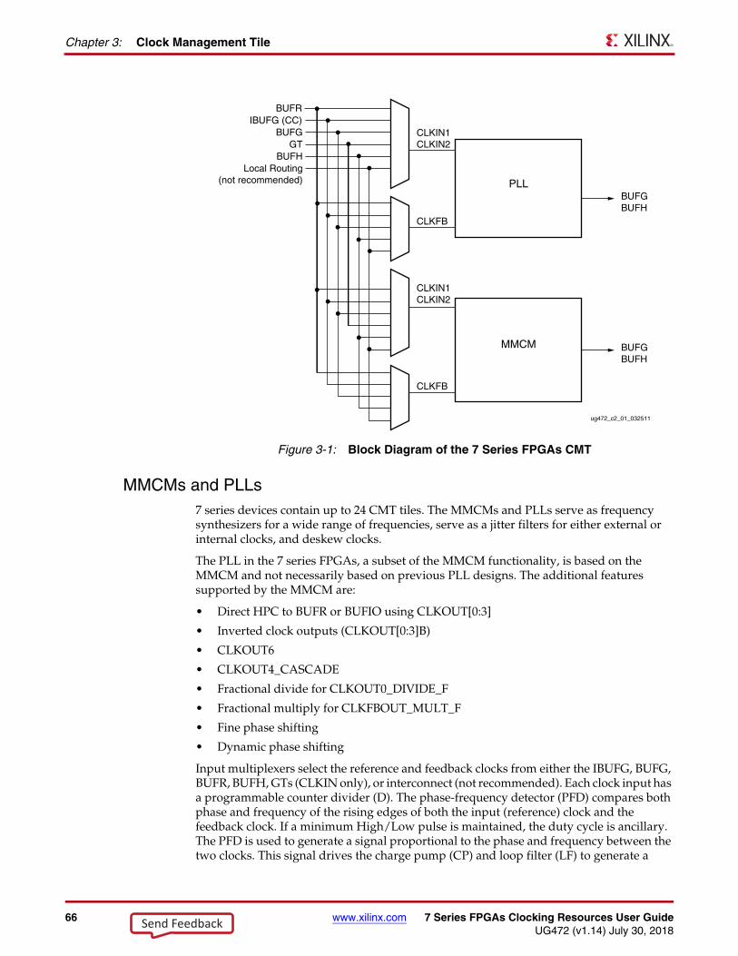
66 www.xilinx.com 7 Series FPGAs Clocking Resources User GuideUG472 (v1.14) July 30, 2018
Chapter 3: Clock Management Tile
MMCMs and PLLs7 series devices contain up to 24 CMT tiles. The MMCMs and PLLs serve as frequency synthesizers for a wide range of frequencies, serve as a jitter filters for either external or internal clocks, and deskew clocks.
The PLL in the 7 series FPGAs, a subset of the MMCM functionality, is based on the MMCM and not necessarily based on previous PLL designs. The additional features supported by the MMCM are:
• Direct HPC to BUFR or BUFIO using CLKOUT[0:3]
• Inverted clock outputs (CLKOUT[0:3]B)
• CLKOUT6
• CLKOUT4_CASCADE
• Fractional divide for CLKOUT0_DIVIDE_F
• Fractional multiply for CLKFBOUT_MULT_F
• Fine phase shifting
• Dynamic phase shifting
Input multiplexers select the reference and feedback clocks from either the IBUFG, BUFG, BUFR, BUFH, GTs (CLKIN only), or interconnect (not recommended). Each clock input has a programmable counter divider (D). The phase-frequency detector (PFD) compares both phase and frequency of the rising edges of both the input (reference) clock and the feedback clock. If a minimum High/Low pulse is maintained, the duty cycle is ancillary. The PFD is used to generate a signal proportional to the phase and frequency between the two clocks. This signal drives the charge pump (CP) and loop filter (LF) to generate a
X-Ref Target - Figure 3-1
Figure 3-1: Block Diagram of the 7 Series FPGAs CMT
GTBUFG
IBUFG (CC)BUFR
BUFHLocal Routing
(not recommended) PLL
MMCM BUFGBUFH
BUFGBUFH
ug472_c2_01_032511
CLKIN1CLKIN2
CLKIN1CLKIN2
CLKFB
CLKFB
Send Feedback
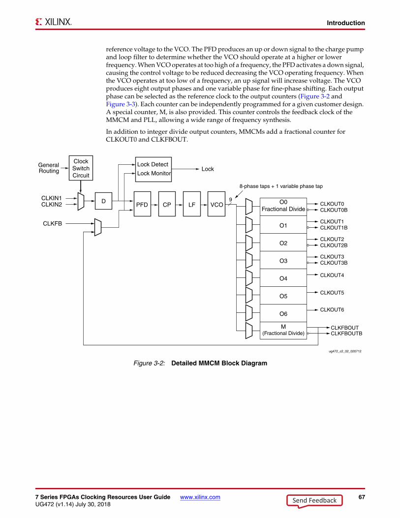
7 Series FPGAs Clocking Resources User Guide www.xilinx.com 67UG472 (v1.14) July 30, 2018
Introduction
reference voltage to the VCO. The PFD produces an up or down signal to the charge pump and loop filter to determine whether the VCO should operate at a higher or lower frequency. When VCO operates at too high of a frequency, the PFD activates a down signal, causing the control voltage to be reduced decreasing the VCO operating frequency. When the VCO operates at too low of a frequency, an up signal will increase voltage. The VCO produces eight output phases and one variable phase for fine-phase shifting. Each output phase can be selected as the reference clock to the output counters (Figure 3-2 and Figure 3-3). Each counter can be independently programmed for a given customer design. A special counter, M, is also provided. This counter controls the feedback clock of the MMCM and PLL, allowing a wide range of frequency synthesis.
In addition to integer divide output counters, MMCMs add a fractional counter for CLKOUT0 and CLKFBOUT.
X-Ref Target - Figure 3-2
Figure 3-2: Detailed MMCM Block Diagram
D
ClockSwitchCircuit
PFD
Lock DetectLock
Lock Monitor
CLKIN1
GeneralRouting
CLKIN2
CLKFB
CLKFBOUT
CLKOUT6
CLKOUT5
CLKOUT4
CLKOUT3BCLKOUT3
CLKOUT2BCLKOUT2
CLKOUT1BCLKOUT1
CLKOUT0BCLKOUT0
CLKFBOUTB
CP LF VCO
8-phase taps + 1 variable phase tap
9 O0Fractional Divide
M(Fractional Divide)
O1
O2
O3
O4
O5
O6
ug472_c2_02_020712
Send Feedback
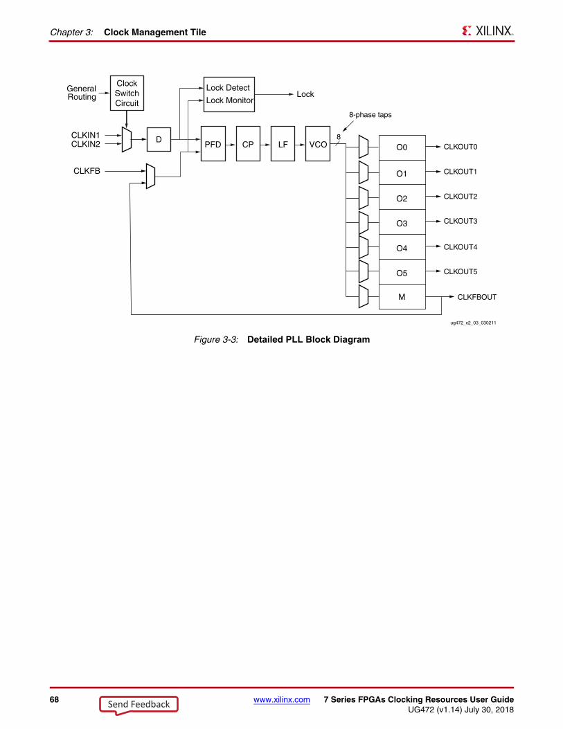
68 www.xilinx.com 7 Series FPGAs Clocking Resources User GuideUG472 (v1.14) July 30, 2018
Chapter 3: Clock Management Tile
X-Ref Target - Figure 3-3
Figure 3-3: Detailed PLL Block Diagram
D
ClockSwitchCircuit
PFD
Lock DetectLock
Lock Monitor
CLKIN1
GeneralRouting
CLKIN2
CLKFB
CLKFBOUT
CLKOUT5
CLKOUT4
CLKOUT3
CLKOUT2
CLKOUT1
CLKOUT0CP LF VCO
8-phase taps
O0
M
O1
O2
O3
O4
O5
ug472_c2_03_030211
8
Send Feedback
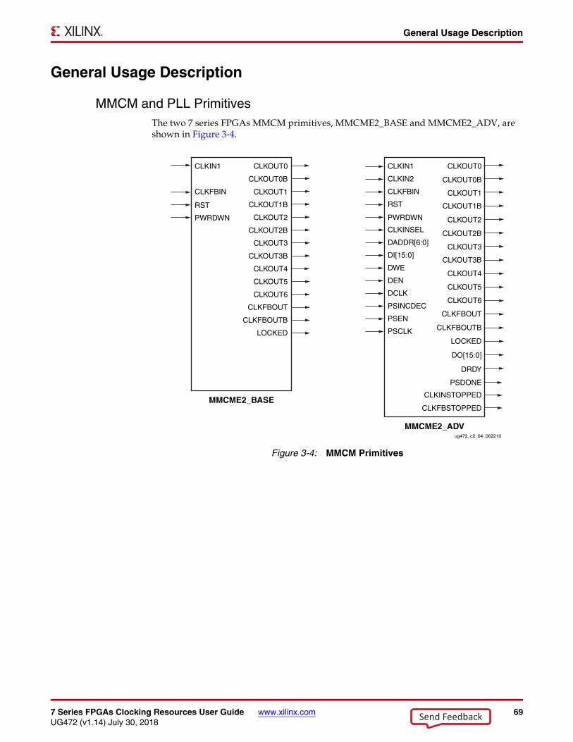
7 Series FPGAs Clocking Resources User Guide www.xilinx.com 69UG472 (v1.14) July 30, 2018
General Usage Description
General Usage Description
MMCM and PLL PrimitivesThe two 7 series FPGAs MMCM primitives, MMCME2_BASE and MMCME2_ADV, are shown in Figure 3-4.X-Ref Target - Figure 3-4
Figure 3-4: MMCM Primitives
CLKIN1
CLKFBIN
RST
CLKOUT0
CLKOUT0B
CLKOUT1
CLKOUT1B
CLKOUT2
CLKOUT2B
CLKOUT3
CLKOUT3B
CLKOUT4
CLKOUT5
CLKOUT6
CLKFBOUT
CLKFBOUTB
LOCKED
MMCME2_BASE
PWRDWN
ug472_c2_04_062210
CLKIN1
CLKIN2
CLKFBIN
CLKINSEL
PWRDWN
DADDR[6:0]
DI[15:0]
DWE
DEN
DCLK
PSINCDEC
PSEN
PSCLK
RST
CLKOUT0
CLKOUT0B
CLKOUT1
CLKOUT1B
CLKOUT2
CLKOUT2B
CLKOUT3
CLKOUT3B
CLKOUT4
CLKOUT5
CLKOUT6
CLKFBOUT
CLKFBOUTB
LOCKED
DO[15:0]
DRDY
PSDONE
CLKINSTOPPED
CLKFBSTOPPED
MMCME2_ADV
Send Feedback
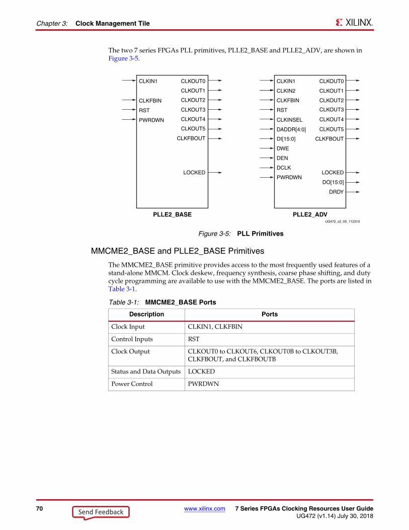
70 www.xilinx.com 7 Series FPGAs Clocking Resources User GuideUG472 (v1.14) July 30, 2018
Chapter 3: Clock Management Tile
The two 7 series FPGAs PLL primitives, PLLE2_BASE and PLLE2_ADV, are shown in Figure 3-5.
MMCME2_BASE and PLLE2_BASE Primitives
The MMCME2_BASE primitive provides access to the most frequently used features of a stand-alone MMCM. Clock deskew, frequency synthesis, coarse phase shifting, and duty cycle programming are available to use with the MMCME2_BASE. The ports are listed in Table 3-1.
X-Ref Target - Figure 3-5
Figure 3-5: PLL Primitives
CLKIN1
CLKFBIN
RST
CLKOUT0
CLKOUT1
CLKOUT2
CLKOUT3
CLKOUT4
CLKOUT5
CLKFBOUT
LOCKED
PLLE2_BASE
PWRDWN
UG472_c2_05_112310
CLKIN1
CLKIN2
CLKFBIN
CLKINSEL
DADDR[4:0]
DI[15:0]
DWE
DEN
DCLK
PWRDWN
RST
CLKOUT0
CLKOUT1
CLKOUT2
CLKOUT3
CLKOUT4
CLKOUT5
CLKFBOUT
LOCKED
DO[15:0]
DRDY
PLLE2_ADV
Table 3-1: MMCME2_BASE Ports
Description Ports
Clock Input CLKIN1, CLKFBIN
Control Inputs RST
Clock Output CLKOUT0 to CLKOUT6, CLKOUT0B to CLKOUT3B, CLKFBOUT, and CLKFBOUTB
Status and Data Outputs LOCKED
Power Control PWRDWN
Send Feedback
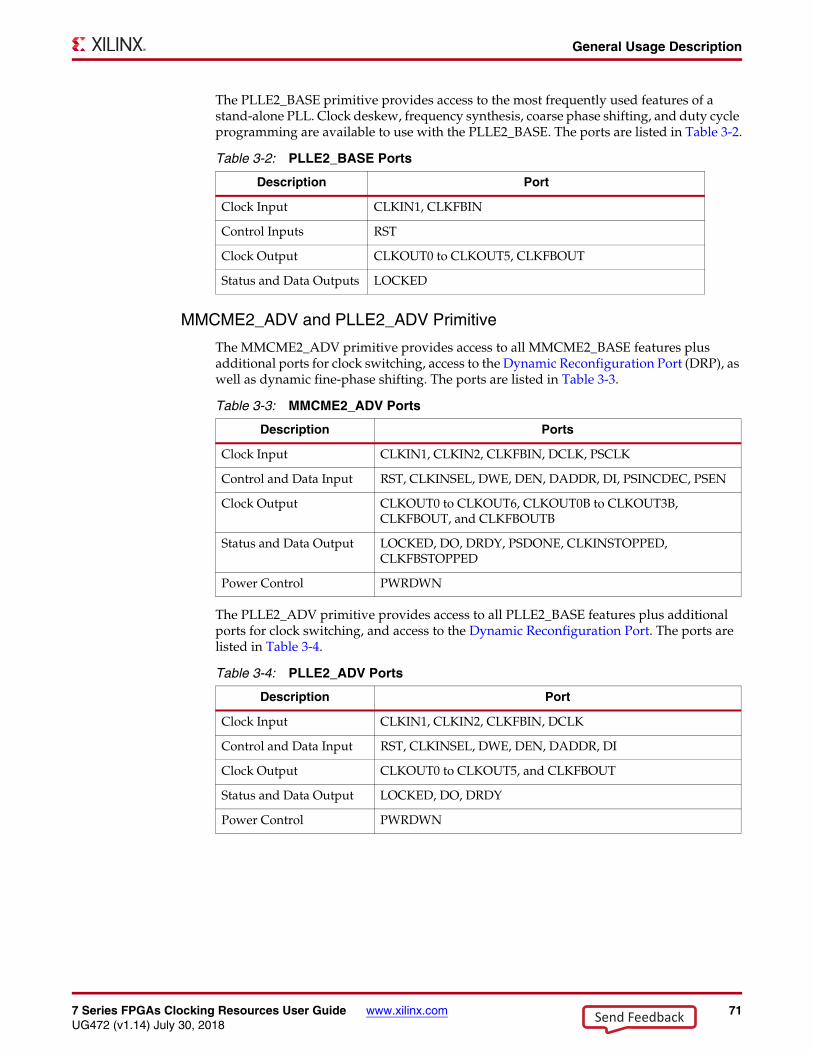
7 Series FPGAs Clocking Resources User Guide www.xilinx.com 71UG472 (v1.14) July 30, 2018
General Usage Description
The PLLE2_BASE primitive provides access to the most frequently used features of a stand-alone PLL. Clock deskew, frequency synthesis, coarse phase shifting, and duty cycle programming are available to use with the PLLE2_BASE. The ports are listed in Table 3-2.
MMCME2_ADV and PLLE2_ADV Primitive
The MMCME2_ADV primitive provides access to all MMCME2_BASE features plus additional ports for clock switching, access to the Dynamic Reconfiguration Port (DRP), as well as dynamic fine-phase shifting. The ports are listed in Table 3-3.
The PLLE2_ADV primitive provides access to all PLLE2_BASE features plus additional ports for clock switching, and access to the Dynamic Reconfiguration Port. The ports are listed in Table 3-4.
Table 3-2: PLLE2_BASE Ports
Description Port
Clock Input CLKIN1, CLKFBIN
Control Inputs RST
Clock Output CLKOUT0 to CLKOUT5, CLKFBOUT
Status and Data Outputs LOCKED
Table 3-3: MMCME2_ADV Ports
Description Ports
Clock Input CLKIN1, CLKIN2, CLKFBIN, DCLK, PSCLK
Control and Data Input RST, CLKINSEL, DWE, DEN, DADDR, DI, PSINCDEC, PSEN
Clock Output CLKOUT0 to CLKOUT6, CLKOUT0B to CLKOUT3B, CLKFBOUT, and CLKFBOUTB
Status and Data Output LOCKED, DO, DRDY, PSDONE, CLKINSTOPPED, CLKFBSTOPPED
Power Control PWRDWN
Table 3-4: PLLE2_ADV Ports
Description Port
Clock Input CLKIN1, CLKIN2, CLKFBIN, DCLK
Control and Data Input RST, CLKINSEL, DWE, DEN, DADDR, DI
Clock Output CLKOUT0 to CLKOUT5, and CLKFBOUT
Status and Data Output LOCKED, DO, DRDY
Power Control PWRDWN
Send Feedback
72 www.xilinx.com 7 Series FPGAs Clocking Resources User GuideUG472 (v1.14) July 30, 2018
Chapter 3: Clock Management Tile
The 7 series FPGAs MMCM and PLL are mixed-signal blocks designed to support clock network deskew, frequency synthesis, and jitter reduction. These three modes of operation are discussed in more detail within this section. The Voltage Controlled Oscillator (VCO) operating frequency can be determined by using the following relationship:
Equation 3-1
Equation 3-2
where the M, D, and O counters are shown in Figure 3-2. The value of M corresponds to the CLKFBOUT_MULT_F setting, the value of D to the DIVCLK_DIVIDE, and O to the CLKOUT_DIVIDE.
The seven “O” counters can be independently programmed. For example, O0 can be programmed to do a divide-by-two while O1 is programmed for a divide by three. The only constraint is that the VCO operating frequency must be the same for all the output counters since a single VCO drives all the counters.
Clock Network DeskewIn many cases, designers do not want to incur the delay on a clock network in their I/O timing budget therefore they use a MMCM/PLL to compensate for the clock network delay. 7 series FPGAs support this feature. A clock output matching the reference clock CLKIN frequency (always CLKFBOUT) is connected to a BUFG in the same half of the device and fed back to the CLKFBIN feedback pin of the MMCM/PLL. The remaining outputs can still be used to divide the clock down for additionally synthesized frequencies. In this case, all output clocks have a defined phase relationship to the input reference clock. The CLKOUT0–CLKOUT3 of either the MMCM or PLL can be used to cascade to other MMCMs/PLLs. However, there is a phase offset on the output clocks between cascaded MMCMs/PLLs.
Frequency Synthesis Only Using Integer DivideThe MMCMs and PLLs can also be used for stand-alone frequency synthesis. In this application, the MMCM/PLL is not used to deskew a clock network, but rather generate an output clock frequency for other blocks. In this mode, the MMCM/PLL feedback paths are internal, which keeps all the routing local, minimizing the jitter. Figure 3-6 shows the MMCM configured as a frequency synthesizer. In this example, an external 33 MHz reference clock is available. The reference clock can be a crystal oscillator or the output of another MMCM. Setting the M counter to 32 makes the VCO oscillate at 1056 MHz (33 MHz x 32). The MMCM outputs are programmed to provide (for example) a 528 MHz processor clock, a 264 MHz gasket clock, a 176 MHz clock, a 132 MHz memory interface clock, a 66 MHz interface, and a 33 MHz interface. In this example, there are no required phase relationships between the reference clock and the output clocks, but there are required relationships between the output clocks.
FVCO FCLKINMD-----×=
FOUT FCLKINM
D O×---------------×=
Send Feedback
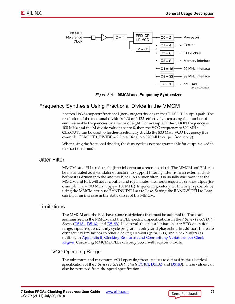
7 Series FPGAs Clocking Resources User Guide www.xilinx.com 73UG472 (v1.14) July 30, 2018
General Usage Description
Frequency Synthesis Using Fractional Divide in the MMCM7 series FPGAs support fractional (non-integer) divides in the CLKOUT0 output path. The resolution of the fractional divide is 1/8 or 0.125, effectively increasing the number of synthesizeable frequencies by a factor of eight. For example, if the CLKIN frequency is 100 MHz and the M divide value is set to 8, then the VCO frequency is 800 MHz. CLKOUT0 can be used to further fractionally divide the 800 MHz VCO frequency (for example, CLKOUT0_DIVIDE = 2.5 resulting in a 320 MHz output frequency).
When using the fractional divider, the duty cycle is not programmable for outputs used in the fractional mode.
Jitter FilterMMCMs and PLLs reduce the jitter inherent on a reference clock. The MMCM and PLL can be instantiated as a standalone function to support filtering jitter from an external clock before it is driven into the another block. As a jitter filter, it is usually assumed that the MMCM and PLL will act as a buffer and regenerates the input frequency on the output (for example, FIN = 100 MHz, FOUT = 100 MHz). In general, greater jitter filtering is possible by using the MMCM attribute BANDWIDTH set to Low. Setting the BANDWIDTH to Low can incur an increase in the static offset of the MMCM.
LimitationsThe MMCM and the PLL have some restrictions that must be adhered to. These are summarized in the MMCM and the PLL electrical specifications in the 7 Series FPGA Data Sheets (DS181, DS182, and DS183). In general, the major limitations are VCO operation range, input frequency, duty cycle programmability, and phase shift. In addition, there are connectivity limitations to other clocking elements (pins, GTs, and clock buffers) as outlined in Appendix B, Clocking Resources and Connectivity Variations per Clock Region. Cascading MMCMs/PLLs can only occur with adjacent CMTs.
VCO Operating Range
The minimum and maximum VCO operating frequencies are defined in the electrical specification of the 7 Series FPGA Data Sheets DS181, DS182, and DS183). These values can also be extracted from the speed specification.
X-Ref Target - Figure 3-6
Figure 3-6: MMCM as a Frequency Synthesizer
D = 133 MHz
ReferenceClock
Processor
Gasket
CLB/Fabric
Memory Interface
66 MHz Interface
not used
PFD, CP,LF, VCO
M = 32
O0 = 2
ug472_c2_06_062711
O1 = 4
O2 = 6
O3 = 8
O4 = 16
O6 = 1
33 MHz InterfaceO5 = 32
Send Feedback
74 www.xilinx.com 7 Series FPGAs Clocking Resources User GuideUG472 (v1.14) July 30, 2018
Chapter 3: Clock Management Tile
Minimum and Maximum Input Frequency
The minimum and maximum CLKIN input frequency are defined in the electrical specification of the 7 Series FPGA Data Sheets (DS181, DS182, and DS183).
Duty Cycle Programmability
Only discrete duty cycles are possible given a VCO operating frequency. Depending on the CLKOUT_DIVIDE value, a minimum and maximum range is possible with a step size that is also depending on the CLKOUT_DIVIDE value. The Clocking Wizard tool gives the possible values for a given CLKOUT_DIVIDE.
Phase Shift
In many cases, there needs to be a phase shift between clocks. The MMCM has multiple options to implement phase shifting. The PLL also has the basic static phase shift capability. Static phase shifting can be achieved by selecting one of the eight VCO output phases with additional fine phase shifting available in the CLKOUT output counters depending on the CLKOUT divide value. In 7 series FPGAs there is also an interpolated phase shifting capability in either fixed or dynamic mode. The MMCM phase shifting capabilities are very powerful which can lead to complex scenarios. By using the Clocking Wizard, the allowable phase shift values are determined based on the MMCM configuration settings.
Static Phase Shift Mode
The static phase shift (SPS) resolution in time units is defined as:
Equation 3-3
Since the VCO can provide eight phase shifted clocks at 45° each; always providing possible settings for 0°, 45°, 90°, 135°, 180°, 225°, 270°, and 315° of phase shift. The higher the VCO frequency is, the smaller the phase-shift resolution. Since the VCO has a distinct operating range, it is possible to bound the phase-shift resolution using from
period.
Each CLKOUT output counter is individually programmable allowing each to have an additional phase-shift resolution in degrees based on the phase of the VCO selected and the CLKOUT counter divide value. The granularity of the CLKOUT phase-shift value can be calculated as 45°/CLKOUT_DIVIDE value. The maximum phase-shift range is also determined by the CLKOUT_DIVIDE value. The maximum phase shift is 360° when CLKOUT_DIVIDE ≤ 64. When CLKOUT_DIVIDE is > 64, the maximum phase shift is:
Equation 3-4
It is possible to phase shift the CLKFBOUT feedback clock. In that case all CLKOUT output clocks are negatively phase shifted with respect to CLKIN.
The two fractional counters (CLKFBOUT and CLKOUT0) also have static phase shift capability. A phase shift step is defined as:
Equation 3-5
For example, if the fractional divide value is 2.125, then a static phase shift step is 360/(2.125 x 8) = 21.176 degrees.
SPS1
8FVCO------------------period or=
D8MFIN------------------period
18FVCOMIN---------------------------- to
18FVCOMAX------------------------------
Maximum Phase Shift 63CLKOUT_ DIVIDE----------------------------------------------------- 360× 7 Phase Shift Value×( )+=
SPS frac( ) 3608 fractional_divide_value×----------------------------------------------------------------------or=
45fractional_divide_value-------------------------------------------------------------
Send Feedback
7 Series FPGAs Clocking Resources User Guide www.xilinx.com 75UG472 (v1.14) July 30, 2018
General Usage Description
Interpolated Fine Phase Shift in Fixed or Dynamic Mode in the MMCM
Interpolated fine phase shift (IFPS) mode in the MMCM has linear shift behavior independent of the CLKOUT_DIVIDE value and the phase shift resolution only depends on the VCO frequency. In this mode the output clocks can be rotated 360° round robin
in linear increments of .
If the VCO runs at 600 MHz, then the phase resolution is approximately (rounded) 30 ps and at 1.6 GHz is approximately (rounded) 11 ps.
The phase shift value can be programmed as a fixed value set during configuration or a dynamic increment/decrement under application control after configuration. The dynamic phase shift is controlled by the PS interface of the MMCME2_ADV. This phase-shift mode equally affects all CLKOUT output clocks that are selected for this mode by setting the USE_FINE_PS attribute to TRUE. In interpolated fine phase-shift mode, a clock must always be connected to the PSCLK pin of the MMCM. Regardless of the interpolated fine phase-shift mode (fixed or dynamic) a clock is in, the clock must always be connected to the PSCLK pin of the MMCM. Each individual CLKOUT counter can independently either select the interpolated phase shift, the previously described static phase-shift mode, or none. Fractional divide is not allowed in either fixed or dynamic interpolated fine phase-shift mode. Fixed or dynamic phase shifting of the feedback path will result in a negative phase shift of all output clocks with respect to CLKIN. The dynamic phase-shift interface cannot be used when the phase-shift mode is set to fixed.
Dynamic Phase Shift Interface in the MMCMThe MMCME2_ADV primitive provides three inputs and one output for dynamic fine-phase shifting. Each CLKOUT and the CLKFBOUT divider can be individually selected for phase shifting. The attributes CLKOUT[0:6]_USE_FINE_PS and CLKFBOUT_USE_FINE_PS select the output clocks to be dynamically phase shifted. The dynamic phase-shift amount is common to all the output clocks selected.
The variable phase shift is controlled by the PSEN, PSINCDEC, PSCLK, and PSDONE ports (Figure 3-7). After the MMCM locks, the initial phase is determined by the CLKOUT_PHASE attribute. Most commonly, no initial phase shift is selected. The phase of the MMCM output clock(s) increments/decrements according to the interaction of PSEN, PSINCDEC, PSCLK, and PSDONE from the initial or previously performed dynamic phase shift. PSEN, PSINCDEC, and PSDONE are synchronous to PSCLK. When PSEN is asserted for one PSCLK clock period, a phase-shift increment/decrement is initiated. When PSINCDEC is High, an increment is initiated and when PSINCDEC is Low, a decrement is initiated. Each increment adds to the phase shift of the MMCM clock outputs by 1/56th of the VCO period. Similarly, each decrement decreases the phase shift by 1/56th of the VCO period. PSEN must be active for one PSCLK period. PSDONE is High for exactly one clock period when the phase shift is complete. The number of PSCLK cycles is deterministic and is always 12 PSCLK cycles. After initiating the phase shift by asserting PSEN, the MMCM output clocks move from their original phase shift to an increment/decrement phase shift. The completion of the increment or decrement is signaled when PSDONE asserts High. After PSDONE has pulsed High, another increment/decrement can be initiated. There is no maximum phase shift or phase-shift overflow. An entire clock period (360 degrees) can always be phase shifted regardless of frequency. When the end of the period is reached, the phase shift wraps around round-robin style.
156FVCO----------------------
Send Feedback
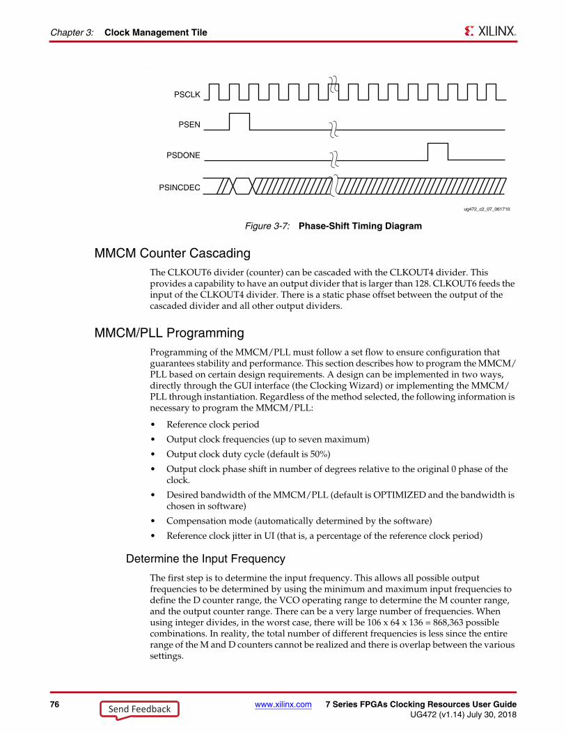
76 www.xilinx.com 7 Series FPGAs Clocking Resources User GuideUG472 (v1.14) July 30, 2018
Chapter 3: Clock Management Tile
,
MMCM Counter CascadingThe CLKOUT6 divider (counter) can be cascaded with the CLKOUT4 divider. This provides a capability to have an output divider that is larger than 128. CLKOUT6 feeds the input of the CLKOUT4 divider. There is a static phase offset between the output of the cascaded divider and all other output dividers.
MMCM/PLL ProgrammingProgramming of the MMCM/PLL must follow a set flow to ensure configuration that guarantees stability and performance. This section describes how to program the MMCM/PLL based on certain design requirements. A design can be implemented in two ways, directly through the GUI interface (the Clocking Wizard) or implementing the MMCM/PLL through instantiation. Regardless of the method selected, the following information is necessary to program the MMCM/PLL:
• Reference clock period
• Output clock frequencies (up to seven maximum)
• Output clock duty cycle (default is 50%)
• Output clock phase shift in number of degrees relative to the original 0 phase of the clock.
• Desired bandwidth of the MMCM/PLL (default is OPTIMIZED and the bandwidth is chosen in software)
• Compensation mode (automatically determined by the software)
• Reference clock jitter in UI (that is, a percentage of the reference clock period)
Determine the Input Frequency
The first step is to determine the input frequency. This allows all possible output frequencies to be determined by using the minimum and maximum input frequencies to define the D counter range, the VCO operating range to determine the M counter range, and the output counter range. There can be a very large number of frequencies. When using integer divides, in the worst case, there will be 106 x 64 x 136 = 868,363 possible combinations. In reality, the total number of different frequencies is less since the entire range of the M and D counters cannot be realized and there is overlap between the various settings.
X-Ref Target - Figure 3-7
Figure 3-7: Phase-Shift Timing Diagram
PSCLK
PSEN
PSDONE
PSINCDEC
ug472_c2_07_061710
Send Feedback
7 Series FPGAs Clocking Resources User Guide www.xilinx.com 77UG472 (v1.14) July 30, 2018
General Usage Description
As an example, consider FIN = 100 MHz, FVCO = between 600 MHz and 1600 MHz, and FPFD = between 10 MHz and 550 MHz.
For a FPFDMIN of 10 MHz, the value of D can only be between 1 and 10.
DMIN (see Equation 3-6) = 1
DMAX (see Equation 3-7) = 10
• For D = 1, M can only have a value between 6 and 16.
• For D = 2, M can only have a value between 12 and 32.
• For D = 3, M can only have a value between 24 and 64.
In addition, D = 1 M = 4 is a subset of D = 2 M = 8, D = 4 M = 16, and D = 8 M = 32 allowing these cases to be dropped. For this case, only D = 1, 3, 5, 6, 7, and 9 are considered since all other D values are subsets of these cases. This drastically reduces the number of possible output frequencies. The output frequencies are sequentially selected. The desired output frequency should be checked against the possible output frequencies generated. Once the first output frequency is determined, an additional constraint can be imposed on the values of M and D. This can further limit the possible output frequencies for the second output frequency. Continue this process until all the output frequencies are selected.
The constraints used to determine the allowed M and D values are shown in the following equations:
Equation 3-6
Equation 3-7
Equation 3-8
Equation 3-9
Determine the M and D Values
Determining the input frequency can result in several possible M and D values. The next step is to determine the optimum M and D values. The starting M value is first determined. This is based off the VCO target frequency, the ideal operating frequency of the VCO.
Equation 3-10
The goal is to find the M value closest to the ideal operating point of the VCO. The minimum D value is used to start the process. The goal is to make D and M values as small as possible while keeping ƒVCO as high as possible.
DMIN roundupfIN
fPFD MAX------------------------=
DMAX rounddownfIN
fPFD MIN-----------------------=
MMIN roundup fVCOMIN
fIN---------------------- DMIN× =
MMAX rounddownfVCOMAX
fIN------------------------ DMAX× =
MIDEAL
DMIN fVCOMAX×fIN
--------------------------------------------=
Send Feedback
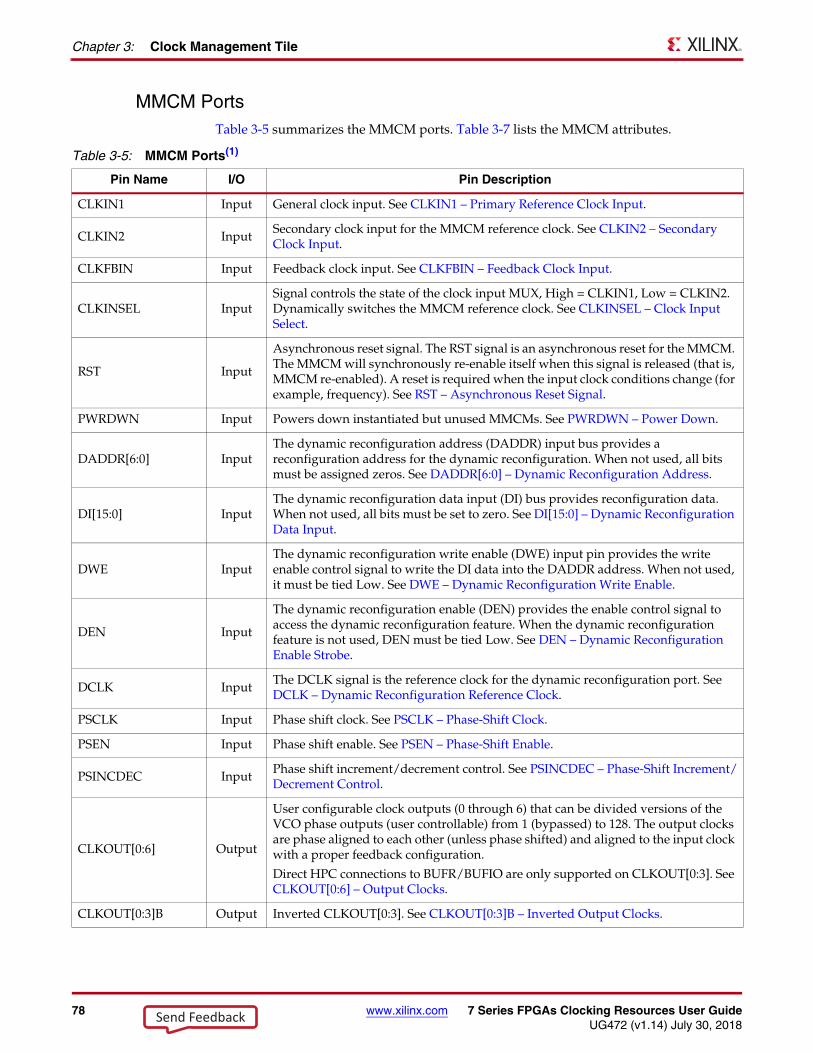
78 www.xilinx.com 7 Series FPGAs Clocking Resources User GuideUG472 (v1.14) July 30, 2018
Chapter 3: Clock Management Tile
MMCM PortsTable 3-5 summarizes the MMCM ports. Table 3-7 lists the MMCM attributes.
Table 3-5: MMCM Ports(1)
Pin Name I/O Pin Description
CLKIN1 Input General clock input. See CLKIN1 – Primary Reference Clock Input.
CLKIN2 InputSecondary clock input for the MMCM reference clock. See CLKIN2 – Secondary Clock Input.
CLKFBIN Input Feedback clock input. See CLKFBIN – Feedback Clock Input.
CLKINSEL InputSignal controls the state of the clock input MUX, High = CLKIN1, Low = CLKIN2. Dynamically switches the MMCM reference clock. See CLKINSEL – Clock Input Select.
RST Input
Asynchronous reset signal. The RST signal is an asynchronous reset for the MMCM. The MMCM will synchronously re-enable itself when this signal is released (that is, MMCM re-enabled). A reset is required when the input clock conditions change (for example, frequency). See RST – Asynchronous Reset Signal.
PWRDWN Input Powers down instantiated but unused MMCMs. See PWRDWN – Power Down.
DADDR[6:0] InputThe dynamic reconfiguration address (DADDR) input bus provides a reconfiguration address for the dynamic reconfiguration. When not used, all bits must be assigned zeros. See DADDR[6:0] – Dynamic Reconfiguration Address.
DI[15:0] InputThe dynamic reconfiguration data input (DI) bus provides reconfiguration data. When not used, all bits must be set to zero. See DI[15:0] – Dynamic Reconfiguration Data Input.
DWE InputThe dynamic reconfiguration write enable (DWE) input pin provides the write enable control signal to write the DI data into the DADDR address. When not used, it must be tied Low. See DWE – Dynamic Reconfiguration Write Enable.
DEN Input
The dynamic reconfiguration enable (DEN) provides the enable control signal to access the dynamic reconfiguration feature. When the dynamic reconfiguration feature is not used, DEN must be tied Low. See DEN – Dynamic Reconfiguration Enable Strobe.
DCLK InputThe DCLK signal is the reference clock for the dynamic reconfiguration port. See DCLK – Dynamic Reconfiguration Reference Clock.
PSCLK Input Phase shift clock. See PSCLK – Phase-Shift Clock.
PSEN Input Phase shift enable. See PSEN – Phase-Shift Enable.
PSINCDEC InputPhase shift increment/decrement control. See PSINCDEC – Phase-Shift Increment/Decrement Control.
CLKOUT[0:6] Output
User configurable clock outputs (0 through 6) that can be divided versions of the VCO phase outputs (user controllable) from 1 (bypassed) to 128. The output clocks are phase aligned to each other (unless phase shifted) and aligned to the input clock with a proper feedback configuration.
Direct HPC connections to BUFR/BUFIO are only supported on CLKOUT[0:3]. See CLKOUT[0:6] – Output Clocks.
CLKOUT[0:3]B Output Inverted CLKOUT[0:3]. See CLKOUT[0:3]B – Inverted Output Clocks.
Send Feedback
7 Series FPGAs Clocking Resources User Guide www.xilinx.com 79UG472 (v1.14) July 30, 2018
General Usage Description
PLL PortsTable 3-6 summarizes the PLL ports.
CLKFBOUT OutputDedicated MMCM feedback output. See CLKFBOUT – Dedicated MMCM and PLL Feedback Output.
CLKFBOUTB Output Inverted CLKFBOUT. See CLKFBOUTB – Inverted CLKFBOUT.
CLKINSTOPPED OutputStatus pin indicating that the input clock has stopped. See CLKINSTOPPED – Input Clock Status.
CLKFBSTOPPED OutputStatus pin indicating that the feedback clock has stopped. See CLKFBSTOPPED – Feedback Clock Status.
LOCKED Output
An output from the MMCM that indicates when the MMCM has achieved phase alignment within a predefined window and frequency matching within a predefined PPM range. The MMCM automatically locks after power on. No extra reset is required. LOCKED will be deasserted if the input clock stops or the phase alignment is violated (for example, input clock phase shift). The MMCM must be reset after LOCKED is deasserted.
DO[15:0] OutputThe dynamic reconfiguration output bus provides MMCM data output when using dynamic reconfiguration. See DO[15:0] – Dynamic Reconfiguration Output Bus.
DRDY OutputThe dynamic reconfiguration ready output (DRDY) provides the response to the DEN signal for the MMCMs dynamic reconfiguration feature. See DRDY – Dynamic Reconfiguration Ready.
PSDONE Output Phase shift done. See PSDONE – Phase Shift Done.
Notes: 1. All control and status signals except PSINCDEC are active-High.
Table 3-5: MMCM Ports(1) (Cont’d)
Pin Name I/O Pin Description
Table 3-6: PLL Ports
Pin Name I/O Pin Description
CLKIN1 Input General clock input.
CLKIN2 Input Secondary clock input to dynamically switch the PLL reference clock.
CLKFBIN Input Feedback clock input.
CLKINSEL InputSignal controls the state of the input multiplexer, High = CLKIN1, Low = CLKIN2. Dynamically switches the PLL reference clock. See CLKINSEL – Clock Input Select.
RST Input
Asynchronous reset signal. The RST signal is an asynchronous reset for the PLL. The PLL will synchronously re-enable itself when this signal is released (that is, PLL re-enabled). A reset is required when the input clock conditions change (for example, frequency).
PWRDWN Input Powers down instantiated but unused PLL. See PWRDWN – Power Down.
DADDR[6:0] InputThe dynamic reconfiguration address (DADDR) input bus provides a reconfiguration address for the dynamic reconfiguration. When not used, all bits must be assigned zeros.
Send Feedback
80 www.xilinx.com 7 Series FPGAs Clocking Resources User GuideUG472 (v1.14) July 30, 2018
Chapter 3: Clock Management Tile
MMCM and PLL Port Descriptions
CLKIN1 – Primary Reference Clock Input
CLKIN1 can be driven by SRCC or MRCC I/O directly within the same clock region, SRCC or MRCC I/O through the CMT backbone in a vertically adjacent clock region, BUFG, BUFR, BUFH, interconnect (not recommended), or directly by a high-speed serial transceiver. When the clock input is coming from another CMT block for cascading CMT functions, only CLKOUT[0:3] can be used.
CLKIN2 – Secondary Clock Input
CLKIN2 is a secondary clock input that is used to dynamically switch the MMCM/PLL reference clock. CLKIN2 can be driven by SRCC or MRCC I/O directly within the same clock region, SRCC or MRCC I/O through the CMT backbone in a vertically adjacent clock region, BUFG, BUFR, BUFH, interconnect (not recommended), or directly by a high-speed serial transceiver.
CLKFBIN – Feedback Clock Input
Must be connected either directly to the CLKFBOUT for internal feedback or IBUFG (through a clock-capable pin for external deskew), BUFG, BUFH, or interconnect (not recommended). For external clock alignment, the feedback path clock buffer type should
DI[15:0] InputThe dynamic reconfiguration data input (DI) bus provides reconfiguration data. When not used, all bits must be set to zero.
DWE InputThe dynamic reconfiguration write enable (DWE) input pin provides the write enable control signal to write the DI data into the DADDR address. When not used, it must be tied Low.
DEN InputThe dynamic reconfiguration enable (DEN) provides the enable control signal to access the dynamic reconfiguration feature. When the dynamic reconfiguration feature is not used, DEN must be tied Low.
DCLK Input The DCLK signal is the reference clock for the dynamic reconfiguration port.
CLKOUT[0:5](1) OutputUser configurable clock outputs (0 through 5) that can be divided versions of the VCO phase outputs (user controllable) from 1 (bypassed) to 128. The input clock and output clocks are phase aligned.
CLKFBOUT Output Dedicated PLL feedback output.
LOCKED Output
An output from the PLL that indicates when the PLL has achieved phase alignment within a predefined window and frequency matching within a predefined PPM range. The PLL automatically locks after power on, no extra reset is required. LOCKED will be deasserted if the input clock stops or the phase alignment is violated (for example, input clock phase shift). The PLL must be reset after LOCKED is deasserted.
DO[15:0] OutputThe dynamic reconfiguration output bus provides PLL data output when using dynamic reconfiguration.
DRDY OutputThe dynamic reconfiguration ready output (DRDY) provides the response to the DEN signal for the PLLs dynamic reconfiguration feature.
Table 3-6: PLL Ports (Cont’d)
Pin Name I/O Pin Description
Send Feedback
7 Series FPGAs Clocking Resources User Guide www.xilinx.com 81UG472 (v1.14) July 30, 2018
General Usage Description
match the forward clock buffer type with the exception of BUFR. BUFR cannot be compensated for.
CLKFBOUT – Dedicated MMCM and PLL Feedback Output
For possible configuration see MMCM and PLL Use Models. CLKFBOUT can also drive logic similar to the CLK0 of the DCM in Virtex-5 FPGAs.
CLKFBOUTB – Inverted CLKFBOUT
This signal should not be used for feedback. It provides an additional, inverted CLKFBOUT output clock. CLKFBOUTB can drive logic similar to the CLK180 clock of the DCM in Virtex-5 FPGAs. Not available in the PLL.
CLKINSEL – Clock Input Select
The CLKINSEL signal controls the state of the clock input MUXes, High = CLKIN1, Low = CLKIN2 (see Reference Clock Switching). The MMCM/PLL must be held in RESET during clock switchover.
RST – Asynchronous Reset Signal
The RST signal is an asynchronous reset for the MMCM/PLL. The MMCM/PLL will be synchronously re-enabled when this signal is deasserted.
PWRDWN – Power Down
Powers down instantiated but currently unused MMCMs/PLLs. This mode can be used to save power for temporarily inactive portions of the design and/or MMCMs/PLLs that are not active in certain system configurations. No MMCM/PLL power is consumed in this mode.
DADDR[6:0] – Dynamic Reconfiguration Address
The dynamic reconfiguration address (DADDR) input bus provides a reconfiguration address for the dynamic reconfiguration. The address value on this bus specifies the 16 configuration bits that are written or read with the next DCLK cycle. When not used, all bits must be assigned zeros.
DI[15:0] – Dynamic Reconfiguration Data Input
The dynamic reconfiguration data input (DI) bus provides reconfiguration data. The value of this bus is written to the configuration cells. The data is presented in the cycle that DEN and DWE are active. The data is captured in a shadow register and written at a later time. DRDY indicates when the DRP port is ready to accept another write. When not used, all bits must be set to zero.
DWE – Dynamic Reconfiguration Write Enable
The dynamic reconfiguration write enable (DWE) input pin provides the write/read enable control signal to write the DI data into or read the DO data from the DADDR address. When not used, it must be tied Low.
DEN – Dynamic Reconfiguration Enable Strobe
The dynamic reconfiguration enable strobe (DEN) provides the enable control signal to access the dynamic reconfiguration feature and enables all DRP port operations. When the dynamic reconfiguration feature is not used, DEN must be tied Low.
Send Feedback
82 www.xilinx.com 7 Series FPGAs Clocking Resources User GuideUG472 (v1.14) July 30, 2018
Chapter 3: Clock Management Tile
DCLK – Dynamic Reconfiguration Reference Clock
The DCLK signal is the reference clock for the dynamic reconfiguration port. The rising edge of this signal is the timing reference for all other port signals. The setup time is specified in the data sheet. There is no hold time requirement for the other input signals relative to the rising edge of the DCLK. The pin can be drive by an IBUF, IBUFG, BUFG, BUFR, or BUFH. There are no dedicated connections to this clock input.
PSCLK – Phase-Shift Clock
This input pin provides the source clock for the dynamic phase-shift interface. All other inputs are synchronous to the positive edge of this clock. The pin can be drive by an IBUF, IBUFG, BUFG, BUFR, or BUFH. There are no dedicated connections to this clock input. Not available in the PLL.
PSEN – Phase-Shift Enable
A dynamic (variable) phase-shift operation is initiated by synchronously asserting this signal. It must be activated for one cycle of the PSCLK. After initiating a phase-shift the phase is gradually shifted until a High pulse on PSDONE indicates that the operation is complete. There are no glitches or sporadic changes during the operation. From the start to the end of the operation the phase is shifted in a continuous analog manner. Not available in the PLL.
PSINCDEC – Phase-Shift Increment/Decrement Control
This input signal synchronously indicates if the dynamic phase shift is an increment or decrement operation (positive or negative phase-shift). PSENCDEC is asserted High for increment and Low for decrement. There is no phase-shift overflow associated with the dynamic phase shift operation. If more 360° or more are shifted, then the phase will wrap around starting at the original phase. Not available in the PLL.
CLKOUT[0:6] – Output Clocks
These user-configurable clock outputs (CLKOUT0 through CLKOUT6 for the MMCM or CLKOUT0 through CLKOUT5 for the PLL) can be divided versions of the VCO phase outputs (user controllable) from 1 (bypassed) to 128. The input clock and output clocks can be phase aligned.
When used with BUFR or BUFIO, only the MMCM can directly connect to the HPC from the clock outputs CLKOUT0 through CLKOUT3. Additionally, CLKOUT0 through CLKOUT3 can connect to the CMT backbone, for cascading MMCMs and PLLs. Similar to driving MMCMs and PLLs from the CCIO pins to adjacent regions (see Clock-Capable Inputs), cascading uses some of the limited resources available in the CMT backbone to connect clocking resources directly in adjacent regions. A phase offset between the cascaded elements within the same column will also result.
For possible configurations see MMCM and PLL Use Models. In the MMCM, CLKOUT0 and CLKFBOUT can be used in fractional divide mode. All CLKOUT outputs can be used in non-fractional mode to provide a static or dynamic phase shift. In fractional mode, only fixed phase-shift is allowed. See Static Phase Shift Mode for more information.
CLKOUT[0:3]B – Inverted Output Clocks
Inverted (180° phase shift) of CLKOUT[0:3]. Not available in the PLL.
Send Feedback
7 Series FPGAs Clocking Resources User Guide www.xilinx.com 83UG472 (v1.14) July 30, 2018
General Usage Description
CLKINSTOPPED – Input Clock Status
Status pin indicating that the input clock has stopped. This signal is asserted within one clock cycle of clock stoppage. The signal is deasserted after the clock has restarted and LOCKED is achieved or the clock is switched to the alternate clock input and the MMCM has re-locked. Not available in the PLL.
CLKFBSTOPPED – Feedback Clock Status
Status pin indicating that the feedback clock has stopped. This signal is asserted within one clock cycle of clock stoppage. The signal is deasserted after the feedback clock has restarted and the MMCM has re-locked. Not available in the PLL.
LOCKED
An output from the MMCM/PLL used to indicate when the MMCM/PLL have achieved phase and frequency alignment of the reference clock and the feedback clock at the input pins. Phase alignment is within a predefined window and frequency matching within a predefined PPM range. The MMCM automatically locks after power on, no extra reset is required. LOCKED will be deasserted within one PFD clock cycle if the input clock stops, the phase alignment is violated (for example, input clock phase shift) or the frequency has changed. The MMCM/PLL must be reset when LOCKED is deasserted. The clock outputs should not be used prior to the assertion of LOCKED.
DO[15:0] – Dynamic Reconfiguration Output Bus
The dynamic reconfiguration output bus provides MMCM data output when using dynamic reconfiguration. If DWE is inactive while DEN is active at the rising edge of DCLK, then this bus holds the content of the configuration cells addressed by DADDR. The DO bus must be captured on the rising edge of DCLK when DRDY is active. The DO bus value is held until the next DRP operation.
DRDY – Dynamic Reconfiguration Ready
The dynamic reconfiguration ready output (DRDY) provides the response to the DEN signal for the MMCMs dynamic reconfiguration feature. This signal indicates that a DEN/DCLK operation has completed.
PSDONE – Phase Shift Done
The phase-shift done output signal is synchronous to the PSCLK. When the current phase-shift operation is completed, the PSDONE signal is asserted for one clock cycle indicating that a new phase-shift cycle can be initiated. Not available in the PLL.
MMCM AttributesTable 3-7 lists the attributes for the MMCME2_BASE and MMCME2_ADV primitives.
Table 3-7: MMCM Attributes
Attribute Type Allowed Values Default Description
BANDWIDTH String HIGHLOWOPTIMIZED
OPTIMIZED Specifies the MMCM programming algorithm affecting the jitter, phase margin and other characteristics of the MMCM.
Send Feedback
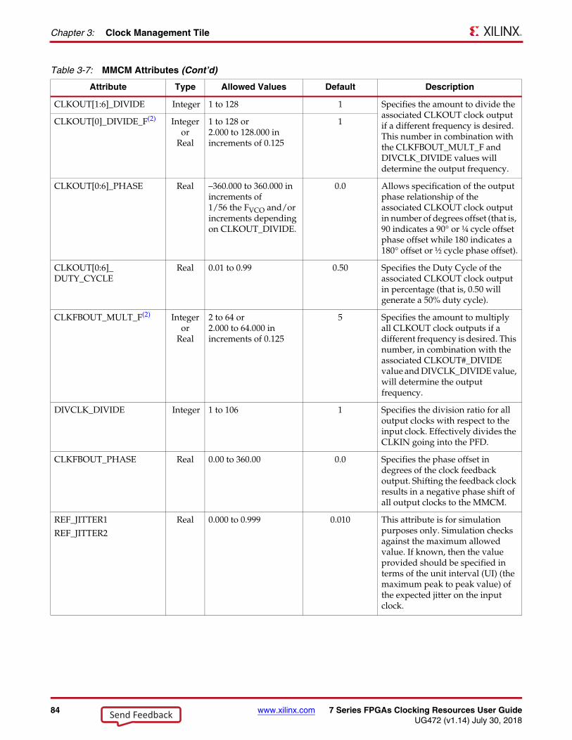
84 www.xilinx.com 7 Series FPGAs Clocking Resources User GuideUG472 (v1.14) July 30, 2018
Chapter 3: Clock Management Tile
CLKOUT[1:6]_DIVIDE Integer 1 to 128 1 Specifies the amount to divide the associated CLKOUT clock output if a different frequency is desired. This number in combination with the CLKFBOUT_MULT_F and DIVCLK_DIVIDE values will determine the output frequency.
CLKOUT[0]_DIVIDE_F(2) Integer or
Real
1 to 128 or2.000 to 128.000 in increments of 0.125
1
CLKOUT[0:6]_PHASE Real –360.000 to 360.000 in increments of 1/56 the FVCO and/or increments depending on CLKOUT_DIVIDE.
0.0 Allows specification of the output phase relationship of the associated CLKOUT clock output in number of degrees offset (that is, 90 indicates a 90° or ¼ cycle offset phase offset while 180 indicates a 180° offset or ½ cycle phase offset).
CLKOUT[0:6]_DUTY_CYCLE
Real 0.01 to 0.99 0.50 Specifies the Duty Cycle of the associated CLKOUT clock output in percentage (that is, 0.50 will generate a 50% duty cycle).
CLKFBOUT_MULT_F(2) Integer or
Real
2 to 64 or2.000 to 64.000 in increments of 0.125
5 Specifies the amount to multiply all CLKOUT clock outputs if a different frequency is desired. This number, in combination with the associated CLKOUT#_DIVIDE value and DIVCLK_DIVIDE value, will determine the output frequency.
DIVCLK_DIVIDE Integer 1 to 106 1 Specifies the division ratio for all output clocks with respect to the input clock. Effectively divides the CLKIN going into the PFD.
CLKFBOUT_PHASE Real 0.00 to 360.00 0.0 Specifies the phase offset in degrees of the clock feedback output. Shifting the feedback clock results in a negative phase shift of all output clocks to the MMCM.
REF_JITTER1
REF_JITTER2
Real 0.000 to 0.999 0.010 This attribute is for simulation purposes only. Simulation checks against the maximum allowed value. If known, then the value provided should be specified in terms of the unit interval (UI) (the maximum peak to peak value) of the expected jitter on the input clock.
Table 3-7: MMCM Attributes (Cont’d)
Attribute Type Allowed Values Default Description
Send Feedback
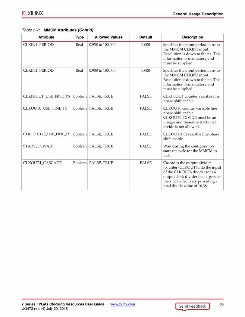
7 Series FPGAs Clocking Resources User Guide www.xilinx.com 85UG472 (v1.14) July 30, 2018
General Usage Description
CLKIN1_PERIOD Real 0.938 to 100.000 0.000 Specifies the input period in ns to the MMCM CLKIN1 input. Resolution is down to the ps. This information is mandatory and must be supplied.
CLKIN2_PERIOD Real 0.938 to 100.000 0.000 Specifies the input period in ns to the MMCM CLKIN2 input. Resolution is down to the ps. This information is mandatory and must be supplied.
CLKFBOUT_USE_FINE_PS Boolean FALSE, TRUE FALSE CLKFBOUT counter variable fine phase shift enable.
CLKOUT0_USE_FINE_PS Boolean FALSE, TRUE FALSE CLKOUT0 counter variable fine phase shift enable. CLKOUT0_DIVIDE must be an integer and therefore fractional divide is not allowed.
CLKOUT[1:6]_USE_FINE_PS Boolean FALSE, TRUE FALSE CLKOUT[1:6] variable fine phase shift enable.
STARTUP_WAIT Boolean FALSE, TRUE FALSE Wait during the configuration start-up cycle for the MMCM to lock.
CLKOUT4_CASCADE Boolean FALSE, TRUE FALSE Cascades the output divider (counter) CLKOUT6 into the input of the CLKOUT4 divider for an output clock divider that is greater than 128, effectively providing a total divide value of 16,384.
Table 3-7: MMCM Attributes (Cont’d)
Attribute Type Allowed Values Default Description
Send Feedback
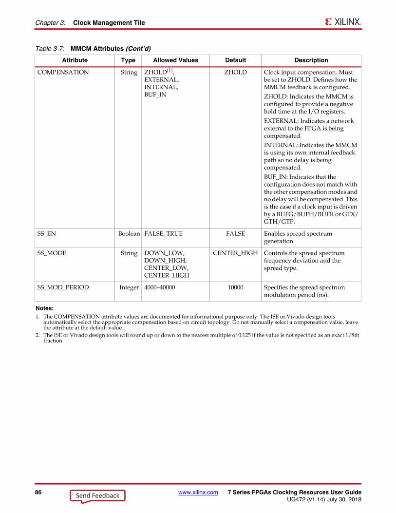
86 www.xilinx.com 7 Series FPGAs Clocking Resources User GuideUG472 (v1.14) July 30, 2018
Chapter 3: Clock Management Tile
COMPENSATION String ZHOLD(1),EXTERNAL, INTERNAL,BUF_IN
ZHOLD Clock input compensation. Must be set to ZHOLD. Defines how the MMCM feedback is configured.
ZHOLD: Indicates the MMCM is configured to provide a negative hold time at the I/O registers.
EXTERNAL: Indicates a network external to the FPGA is being compensated.
INTERNAL: Indicates the MMCM is using its own internal feedback path so no delay is being compensated.
BUF_IN: Indicates that the configuration does not match with the other compensation modes and no delay will be compensated. This is the case if a clock input is driven by a BUFG/BUFH/BUFR or GTX/GTH/GTP.
SS_EN Boolean FALSE, TRUE FALSE Enables spread spectrum generation.
SS_MODE String DOWN_LOW,DOWN_HIGH,CENTER_LOW,CENTER_HIGH
CENTER_HIGH Controls the spread spectrum frequency deviation and the spread type.
SS_MOD_PERIOD Integer 4000–40000 10000 Specifies the spread spectrum modulation period (ns).
Notes: 1. The COMPENSATION attribute values are documented for informational purpose only. The ISE or Vivado design tools
automatically select the appropriate compensation based on circuit topology. Do not manually select a compensation value, leave the attribute at the default value.
2. The ISE or Vivado design tools will round up or down to the nearest multiple of 0.125 if the value is not specified as an exact 1/8th fraction.
Table 3-7: MMCM Attributes (Cont’d)
Attribute Type Allowed Values Default Description
Send Feedback
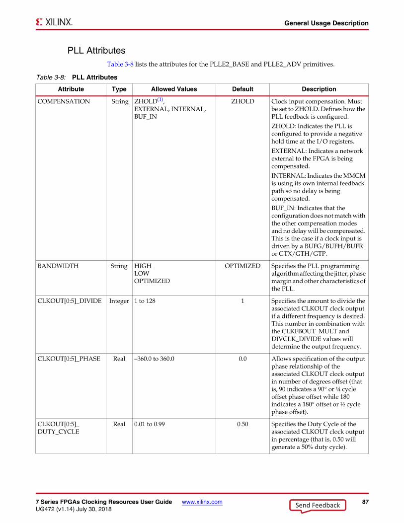
7 Series FPGAs Clocking Resources User Guide www.xilinx.com 87UG472 (v1.14) July 30, 2018
General Usage Description
PLL AttributesTable 3-8 lists the attributes for the PLLE2_BASE and PLLE2_ADV primitives.
Table 3-8: PLL Attributes
Attribute Type Allowed Values Default Description
COMPENSATION String ZHOLD(1),EXTERNAL, INTERNAL,BUF_IN
ZHOLD Clock input compensation. Must be set to ZHOLD. Defines how the PLL feedback is configured.
ZHOLD: Indicates the PLL is configured to provide a negative hold time at the I/O registers.
EXTERNAL: Indicates a network external to the FPGA is being compensated.
INTERNAL: Indicates the MMCM is using its own internal feedback path so no delay is being compensated.
BUF_IN: Indicates that the configuration does not match with the other compensation modes and no delay will be compensated. This is the case if a clock input is driven by a BUFG/BUFH/BUFR or GTX/GTH/GTP.
BANDWIDTH String HIGHLOWOPTIMIZED
OPTIMIZED Specifies the PLL programming algorithm affecting the jitter, phase margin and other characteristics of the PLL.
CLKOUT[0:5]_DIVIDE Integer 1 to 128 1 Specifies the amount to divide the associated CLKOUT clock output if a different frequency is desired. This number in combination with the CLKFBOUT_MULT and DIVCLK_DIVIDE values will determine the output frequency.
CLKOUT[0:5]_PHASE Real –360.0 to 360.0 0.0 Allows specification of the output phase relationship of the associated CLKOUT clock output in number of degrees offset (that is, 90 indicates a 90° or ¼ cycle offset phase offset while 180 indicates a 180° offset or ½ cycle phase offset).
CLKOUT[0:5]_DUTY_CYCLE
Real 0.01 to 0.99 0.50 Specifies the Duty Cycle of the associated CLKOUT clock output in percentage (that is, 0.50 will generate a 50% duty cycle).
Send Feedback
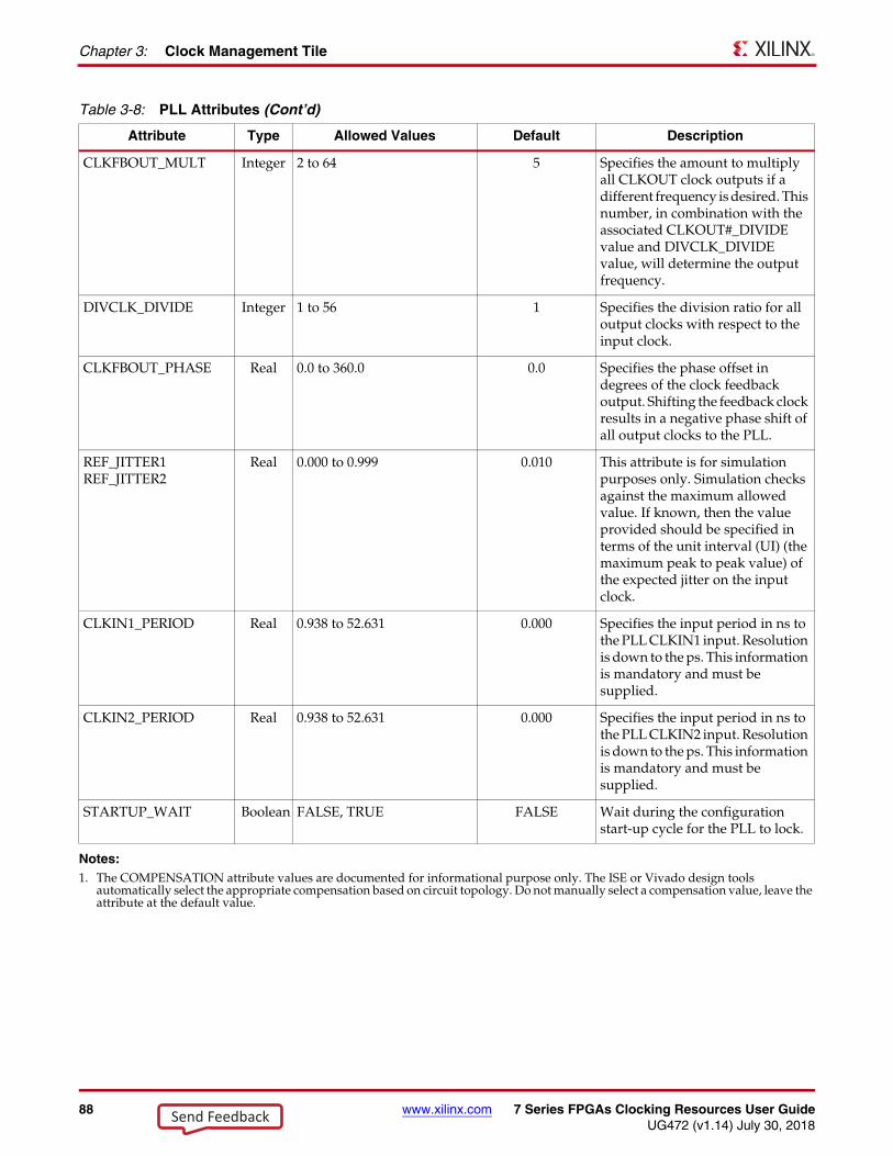
88 www.xilinx.com 7 Series FPGAs Clocking Resources User GuideUG472 (v1.14) July 30, 2018
Chapter 3: Clock Management Tile
CLKFBOUT_MULT Integer 2 to 64 5 Specifies the amount to multiply all CLKOUT clock outputs if a different frequency is desired. This number, in combination with the associated CLKOUT#_DIVIDE value and DIVCLK_DIVIDE value, will determine the output frequency.
DIVCLK_DIVIDE Integer 1 to 56 1 Specifies the division ratio for all output clocks with respect to the input clock.
CLKFBOUT_PHASE Real 0.0 to 360.0 0.0 Specifies the phase offset in degrees of the clock feedback output. Shifting the feedback clock results in a negative phase shift of all output clocks to the PLL.
REF_JITTER1REF_JITTER2
Real 0.000 to 0.999 0.010 This attribute is for simulation purposes only. Simulation checks against the maximum allowed value. If known, then the value provided should be specified in terms of the unit interval (UI) (the maximum peak to peak value) of the expected jitter on the input clock.
CLKIN1_PERIOD Real 0.938 to 52.631 0.000 Specifies the input period in ns to the PLL CLKIN1 input. Resolution is down to the ps. This information is mandatory and must be supplied.
CLKIN2_PERIOD Real 0.938 to 52.631 0.000 Specifies the input period in ns to the PLL CLKIN2 input. Resolution is down to the ps. This information is mandatory and must be supplied.
STARTUP_WAIT Boolean FALSE, TRUE FALSE Wait during the configuration start-up cycle for the PLL to lock.
Notes: 1. The COMPENSATION attribute values are documented for informational purpose only. The ISE or Vivado design tools
automatically select the appropriate compensation based on circuit topology. Do not manually select a compensation value, leave the attribute at the default value.
Table 3-8: PLL Attributes (Cont’d)
Attribute Type Allowed Values Default Description
Send Feedback
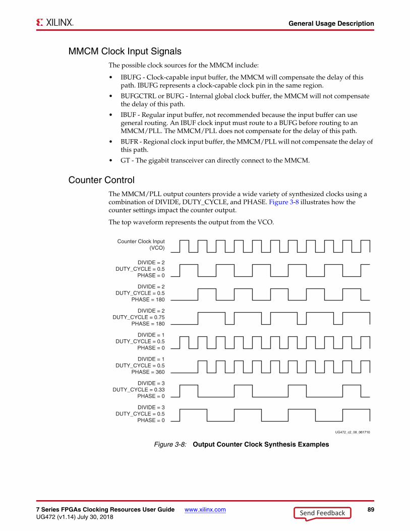
7 Series FPGAs Clocking Resources User Guide www.xilinx.com 89UG472 (v1.14) July 30, 2018
General Usage Description
MMCM Clock Input SignalsThe possible clock sources for the MMCM include:
• IBUFG - Clock-capable input buffer, the MMCM will compensate the delay of this path. IBUFG represents a clock-capable clock pin in the same region.
• BUFGCTRL or BUFG - Internal global clock buffer, the MMCM will not compensate the delay of this path.
• IBUF - Regular input buffer, not recommended because the input buffer can use general routing. An IBUF clock input must route to a BUFG before routing to an MMCM/PLL. The MMCM/PLL does not compensate for the delay of this path.
• BUFR - Regional clock input buffer, the MMCM/PLL will not compensate the delay of this path.
• GT - The gigabit transceiver can directly connect to the MMCM.
Counter ControlThe MMCM/PLL output counters provide a wide variety of synthesized clocks using a combination of DIVIDE, DUTY_CYCLE, and PHASE. Figure 3-8 illustrates how the counter settings impact the counter output.
The top waveform represents the output from the VCO.X-Ref Target - Figure 3-8
Figure 3-8: Output Counter Clock Synthesis Examples
Counter Clock Input(VCO)
DIVIDE = 2DUTY_CYCLE = 0.5
PHASE = 0
DIVIDE = 2DUTY_CYCLE = 0.5
PHASE = 180
DIVIDE = 2DUTY_CYCLE = 0.75
PHASE = 180
DIVIDE = 1DUTY_CYCLE = 0.5
PHASE = 0
DIVIDE = 1DUTY_CYCLE = 0.5
PHASE = 360
DIVIDE = 3DUTY_CYCLE = 0.33
PHASE = 0
DIVIDE = 3DUTY_CYCLE = 0.5
PHASE = 0
UG472_c2_08_061710
Send Feedback
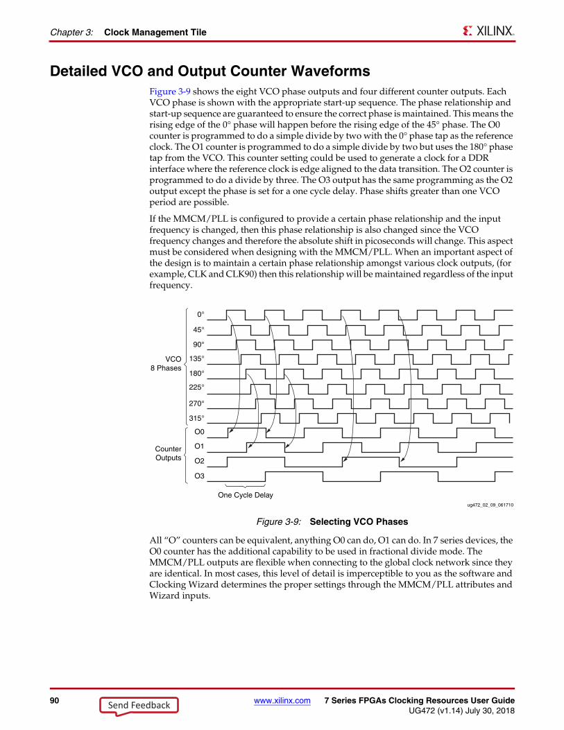
90 www.xilinx.com 7 Series FPGAs Clocking Resources User GuideUG472 (v1.14) July 30, 2018
Chapter 3: Clock Management Tile
Detailed VCO and Output Counter WaveformsFigure 3-9 shows the eight VCO phase outputs and four different counter outputs. Each VCO phase is shown with the appropriate start-up sequence. The phase relationship and start-up sequence are guaranteed to ensure the correct phase is maintained. This means the rising edge of the 0° phase will happen before the rising edge of the 45° phase. The O0 counter is programmed to do a simple divide by two with the 0° phase tap as the reference clock. The O1 counter is programmed to do a simple divide by two but uses the 180° phase tap from the VCO. This counter setting could be used to generate a clock for a DDR interface where the reference clock is edge aligned to the data transition. The O2 counter is programmed to do a divide by three. The O3 output has the same programming as the O2 output except the phase is set for a one cycle delay. Phase shifts greater than one VCO period are possible.
If the MMCM/PLL is configured to provide a certain phase relationship and the input frequency is changed, then this phase relationship is also changed since the VCO frequency changes and therefore the absolute shift in picoseconds will change. This aspect must be considered when designing with the MMCM/PLL. When an important aspect of the design is to maintain a certain phase relationship amongst various clock outputs, (for example, CLK and CLK90) then this relationship will be maintained regardless of the input frequency.
All “O” counters can be equivalent, anything O0 can do, O1 can do. In 7 series devices, the O0 counter has the additional capability to be used in fractional divide mode. The MMCM/PLL outputs are flexible when connecting to the global clock network since they are identical. In most cases, this level of detail is imperceptible to you as the software and Clocking Wizard determines the proper settings through the MMCM/PLL attributes and Wizard inputs.
X-Ref Target - Figure 3-9
Figure 3-9: Selecting VCO Phases
One Cycle Delay
CounterOutputs
VCO8 Phases
0°
45°
90°
135°
180°
225°
270°
315°
O0
O1
O2
O3
ug472_02_09_061710
Send Feedback
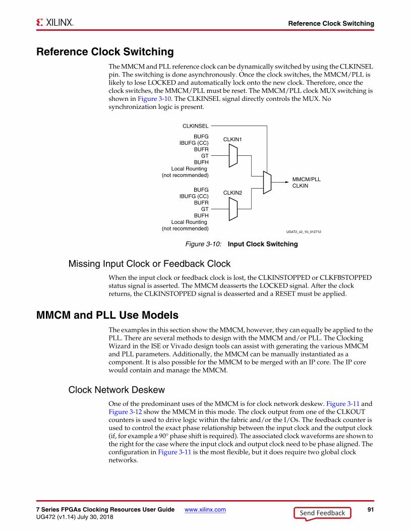
7 Series FPGAs Clocking Resources User Guide www.xilinx.com 91UG472 (v1.14) July 30, 2018
Reference Clock Switching
Reference Clock SwitchingThe MMCM and PLL reference clock can be dynamically switched by using the CLKINSEL pin. The switching is done asynchronously. Once the clock switches, the MMCM/PLL is likely to lose LOCKED and automatically lock onto the new clock. Therefore, once the clock switches, the MMCM/PLL must be reset. The MMCM/PLL clock MUX switching is shown in Figure 3-10. The CLKINSEL signal directly controls the MUX. No synchronization logic is present.
Missing Input Clock or Feedback ClockWhen the input clock or feedback clock is lost, the CLKINSTOPPED or CLKFBSTOPPED status signal is asserted. The MMCM deasserts the LOCKED signal. After the clock returns, the CLKINSTOPPED signal is deasserted and a RESET must be applied.
MMCM and PLL Use ModelsThe examples in this section show the MMCM, however, they can equally be applied to the PLL. There are several methods to design with the MMCM and/or PLL. The Clocking Wizard in the ISE or Vivado design tools can assist with generating the various MMCM and PLL parameters. Additionally, the MMCM can be manually instantiated as a component. It is also possible for the MMCM to be merged with an IP core. The IP core would contain and manage the MMCM.
Clock Network DeskewOne of the predominant uses of the MMCM is for clock network deskew. Figure 3-11 and Figure 3-12 show the MMCM in this mode. The clock output from one of the CLKOUT counters is used to drive logic within the fabric and/or the I/Os. The feedback counter is used to control the exact phase relationship between the input clock and the output clock (if, for example a 90° phase shift is required). The associated clock waveforms are shown to the right for the case where the input clock and output clock need to be phase aligned. The configuration in Figure 3-11 is the most flexible, but it does require two global clock networks.
X-Ref Target - Figure 3-10
Figure 3-10: Input Clock Switching
BUFGIBUFG (CC)
BUFRGT
BUFHLocal Rounting
(not recommended)
BUFGIBUFG (CC)
BUFRGT
BUFHLocal Rounting
(not recommended)UG472_c2_10_012712
CLKINSEL
CLKIN1
CLKIN2
MMCM/PLLCLKIN
Send Feedback
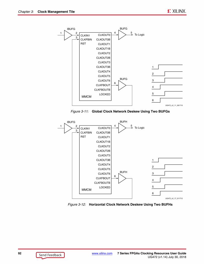
92 www.xilinx.com 7 Series FPGAs Clocking Resources User GuideUG472 (v1.14) July 30, 2018
Chapter 3: Clock Management Tile
X-Ref Target - Figure 3-11
Figure 3-11: Global Clock Network Deskew Using Two BUFGs
X-Ref Target - Figure 3-12
Figure 3-12: Horizontal Clock Network Deskew Using Two BUFHs
CLKIN1
CLKFBIN
RST
MMCM
IBUFG
1 2 4 5
3
BUFG
BUFG
To Logic
6
UG472_c2_11_061710
6
5
4
3
2
1
CLKOUT0
CLKOUT0B
CLKOUT1
CLKOUT1B
CLKOUT2
CLKOUT2B
CLKOUT3
CLKOUT3B
CLKOUT4
CLKOUT5
CLKOUT6
CLKFBOUT
CLKFBOUTB
LOCKED
CLKIN1
CLKFBIN
RST
MMCM
IBUFG
1 2 4 5
3
BUFH
BUFH
To Logic
6
UG472_c2_17_011712
6
5
4
3
2
1
CLKOUT0
CLKOUT0B
CLKOUT1
CLKOUT1B
CLKOUT2
CLKOUT2B
CLKOUT3
CLKOUT3B
CLKOUT4
CLKOUT5
CLKOUT6
CLKFBOUT
CLKFBOUTB
LOCKED
Send Feedback
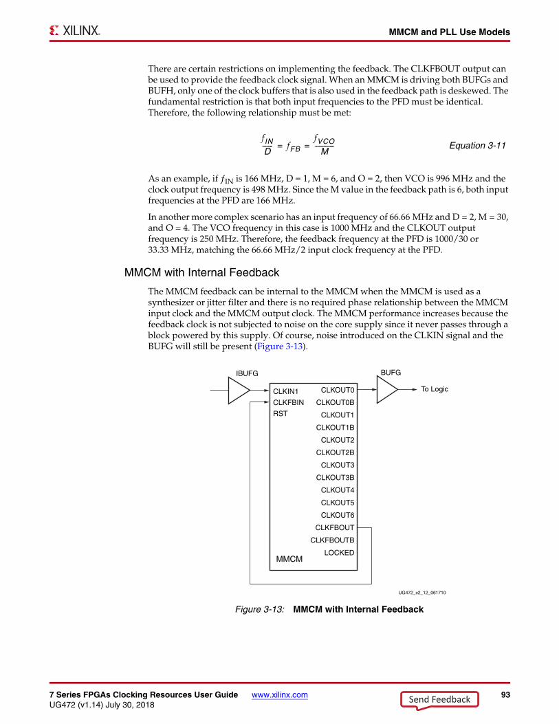
7 Series FPGAs Clocking Resources User Guide www.xilinx.com 93UG472 (v1.14) July 30, 2018
MMCM and PLL Use Models
There are certain restrictions on implementing the feedback. The CLKFBOUT output can be used to provide the feedback clock signal. When an MMCM is driving both BUFGs and BUFH, only one of the clock buffers that is also used in the feedback path is deskewed. The fundamental restriction is that both input frequencies to the PFD must be identical. Therefore, the following relationship must be met:
Equation 3-11
As an example, if ƒIN is 166 MHz, D = 1, M = 6, and O = 2, then VCO is 996 MHz and the clock output frequency is 498 MHz. Since the M value in the feedback path is 6, both input frequencies at the PFD are 166 MHz.
In another more complex scenario has an input frequency of 66.66 MHz and D = 2, M = 30, and O = 4. The VCO frequency in this case is 1000 MHz and the CLKOUT output frequency is 250 MHz. Therefore, the feedback frequency at the PFD is 1000/30 or 33.33 MHz, matching the 66.66 MHz/2 input clock frequency at the PFD.
MMCM with Internal Feedback
The MMCM feedback can be internal to the MMCM when the MMCM is used as a synthesizer or jitter filter and there is no required phase relationship between the MMCM input clock and the MMCM output clock. The MMCM performance increases because the feedback clock is not subjected to noise on the core supply since it never passes through a block powered by this supply. Of course, noise introduced on the CLKIN signal and the BUFG will still be present (Figure 3-13).
fIND------- fFB
fVCO
M-------------= =
X-Ref Target - Figure 3-13
Figure 3-13: MMCM with Internal Feedback
CLKIN1
CLKFBIN
RST
MMCM
IBUFG BUFG
To LogicCLKOUT0
CLKOUT0B
CLKOUT1
CLKOUT1B
CLKOUT2
CLKOUT2B
CLKOUT3
CLKOUT3B
CLKOUT4
CLKOUT5
CLKOUT6
CLKFBOUT
CLKFBOUTB
LOCKED
UG472_c2_12_061710
Send Feedback
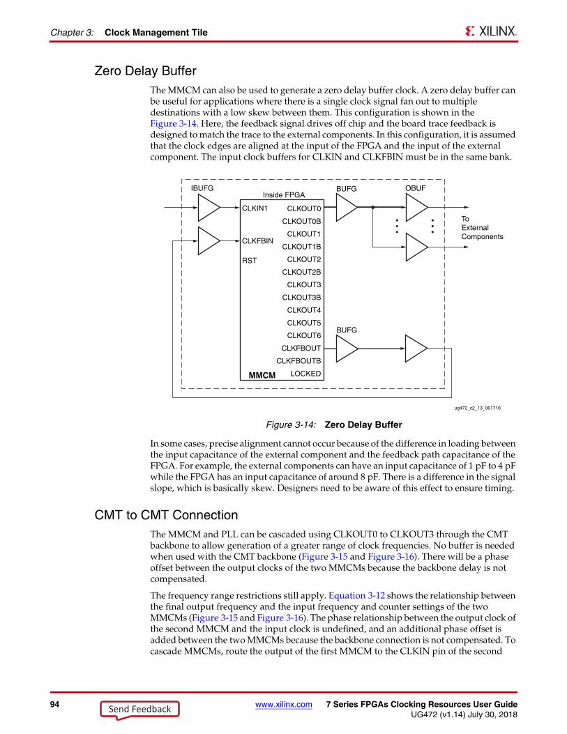
94 www.xilinx.com 7 Series FPGAs Clocking Resources User GuideUG472 (v1.14) July 30, 2018
Chapter 3: Clock Management Tile
Zero Delay BufferThe MMCM can also be used to generate a zero delay buffer clock. A zero delay buffer can be useful for applications where there is a single clock signal fan out to multiple destinations with a low skew between them. This configuration is shown in the Figure 3-14. Here, the feedback signal drives off chip and the board trace feedback is designed to match the trace to the external components. In this configuration, it is assumed that the clock edges are aligned at the input of the FPGA and the input of the external component. The input clock buffers for CLKIN and CLKFBIN must be in the same bank.
In some cases, precise alignment cannot occur because of the difference in loading between the input capacitance of the external component and the feedback path capacitance of the FPGA. For example, the external components can have an input capacitance of 1 pF to 4 pF while the FPGA has an input capacitance of around 8 pF. There is a difference in the signal slope, which is basically skew. Designers need to be aware of this effect to ensure timing.
CMT to CMT ConnectionThe MMCM and PLL can be cascaded using CLKOUT0 to CLKOUT3 through the CMT backbone to allow generation of a greater range of clock frequencies. No buffer is needed when used with the CMT backbone (Figure 3-15 and Figure 3-16). There will be a phase offset between the output clocks of the two MMCMs because the backbone delay is not compensated.
The frequency range restrictions still apply. Equation 3-12 shows the relationship between the final output frequency and the input frequency and counter settings of the two MMCMs (Figure 3-15 and Figure 3-16). The phase relationship between the output clock of the second MMCM and the input clock is undefined, and an additional phase offset is added between the two MMCMs because the backbone connection is not compensated. To cascade MMCMs, route the output of the first MMCM to the CLKIN pin of the second
X-Ref Target - Figure 3-14
Figure 3-14: Zero Delay Buffer
CLKIN1
CLKFBIN
RST
MMCM
IBUFGInside FPGA
OBUF
ToExternalComponents
BUFG
BUFG
CLKOUT0
CLKOUT0B
CLKOUT1
CLKOUT1B
CLKOUT2
CLKOUT2B
CLKOUT3
CLKOUT3B
CLKOUT4
CLKOUT5
CLKOUT6
CLKFBOUT
CLKFBOUTB
LOCKED
ug472_c2_13_061710
Send Feedback
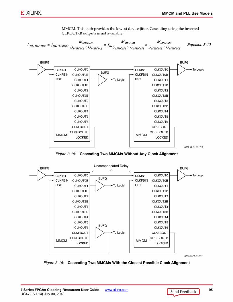
7 Series FPGAs Clocking Resources User Guide www.xilinx.com 95UG472 (v1.14) July 30, 2018
MMCM and PLL Use Models
MMCM. This path provides the lowest device jitter. Cascading using the inverted CLKOUTxB outputs is not available.
Equation 3-12fOUTMMCM2 fOUTMMCM1
MMMCM2
DMMCM2 OMMCM2×-------------------------------------------------- fIN
MMMCM1
DMMCM1 OMMCM1×--------------------------------------------------
MMMCM2
DMMCM2 OMMCM2×--------------------------------------------------×= =
X-Ref Target - Figure 3-15
Figure 3-15: Cascading Two MMCMs Without Any Clock Alignment
X-Ref Target - Figure 3-16
Figure 3-16: Cascading Two MMCMs With the Closest Possible Clock Alignment
CLKIN1
CLKFBIN
RST
CLKIN1
CLKFBIN
RST
MMCM
To Logic
IBUFG BUFG
To Logic
BUFG
ug472_c2_14_061710
CLKOUT0
CLKOUT0B
CLKOUT1
CLKOUT1B
CLKOUT2
CLKOUT2B
CLKOUT3
CLKOUT3B
CLKOUT4
CLKOUT5
CLKOUT6
CLKFBOUT
CLKFBOUTB
LOCKEDMMCM
CLKOUT0
CLKOUT0B
CLKOUT1
CLKOUT1B
CLKOUT2
CLKOUT2B
CLKOUT3
CLKOUT3B
CLKOUT4
CLKOUT5
CLKOUT6
CLKFBOUT
CLKFBOUTB
LOCKED
CLKIN1
CLKFBIN
RST
CLKIN1
CLKFBIN
RST
MMCM
To Logic
IBUFG BUFG
To Logic
BUFG
ug472_c2_15_042611
CLKOUT0
CLKOUT0B
CLKOUT1
CLKOUT1B
CLKOUT2
CLKOUT2B
CLKOUT3
CLKOUT3B
CLKOUT4
CLKOUT5
CLKOUT6
CLKFBOUT
CLKFBOUTB
LOCKEDMMCM
Uncompensated Delay
To Logic
BUFG
CLKOUT0
CLKOUT0B
CLKOUT1
CLKOUT1B
CLKOUT2
CLKOUT2B
CLKOUT3
CLKOUT3B
CLKOUT4
CLKOUT5
CLKOUT6
CLKFBOUT
CLKFBOUTB
LOCKED
Send Feedback
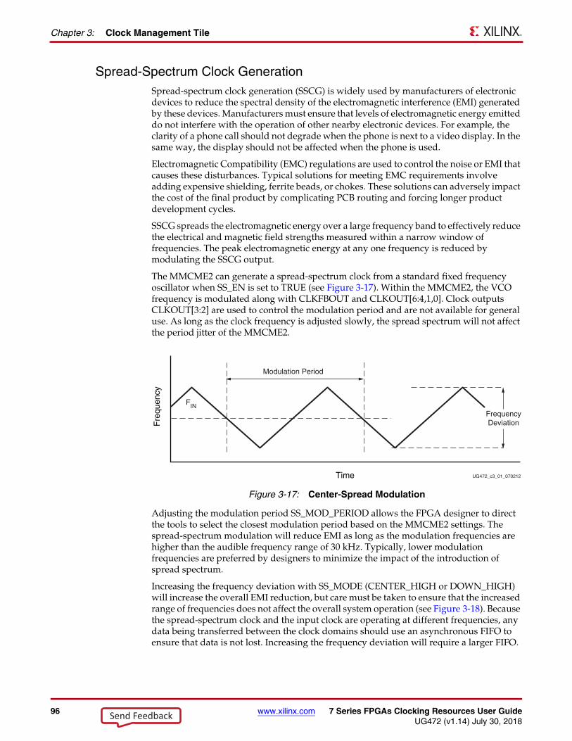
96 www.xilinx.com 7 Series FPGAs Clocking Resources User GuideUG472 (v1.14) July 30, 2018
Chapter 3: Clock Management Tile
Spread-Spectrum Clock GenerationSpread-spectrum clock generation (SSCG) is widely used by manufacturers of electronic devices to reduce the spectral density of the electromagnetic interference (EMI) generated by these devices. Manufacturers must ensure that levels of electromagnetic energy emitted do not interfere with the operation of other nearby electronic devices. For example, the clarity of a phone call should not degrade when the phone is next to a video display. In the same way, the display should not be affected when the phone is used.
Electromagnetic Compatibility (EMC) regulations are used to control the noise or EMI that causes these disturbances. Typical solutions for meeting EMC requirements involve adding expensive shielding, ferrite beads, or chokes. These solutions can adversely impact the cost of the final product by complicating PCB routing and forcing longer product development cycles.
SSCG spreads the electromagnetic energy over a large frequency band to effectively reduce the electrical and magnetic field strengths measured within a narrow window of frequencies. The peak electromagnetic energy at any one frequency is reduced by modulating the SSCG output.
The MMCME2 can generate a spread-spectrum clock from a standard fixed frequency oscillator when SS_EN is set to TRUE (see Figure 3-17). Within the MMCME2, the VCO frequency is modulated along with CLKFBOUT and CLKOUT[6:4,1,0]. Clock outputs CLKOUT[3:2] are used to control the modulation period and are not available for general use. As long as the clock frequency is adjusted slowly, the spread spectrum will not affect the period jitter of the MMCME2.
Adjusting the modulation period SS_MOD_PERIOD allows the FPGA designer to direct the tools to select the closest modulation period based on the MMCME2 settings. The spread-spectrum modulation will reduce EMI as long as the modulation frequencies are higher than the audible frequency range of 30 kHz. Typically, lower modulation frequencies are preferred by designers to minimize the impact of the introduction of spread spectrum.
Increasing the frequency deviation with SS_MODE (CENTER_HIGH or DOWN_HIGH) will increase the overall EMI reduction, but care must be taken to ensure that the increased range of frequencies does not affect the overall system operation (see Figure 3-18). Because the spread-spectrum clock and the input clock are operating at different frequencies, any data being transferred between the clock domains should use an asynchronous FIFO to ensure that data is not lost. Increasing the frequency deviation will require a larger FIFO.
X-Ref Target - Figure 3-17
Figure 3-17: Center-Spread Modulation
Modulation Period
FrequencyDeviation
UG472_c3_01_070212
FIN
Fre
quen
cy
Time
Send Feedback
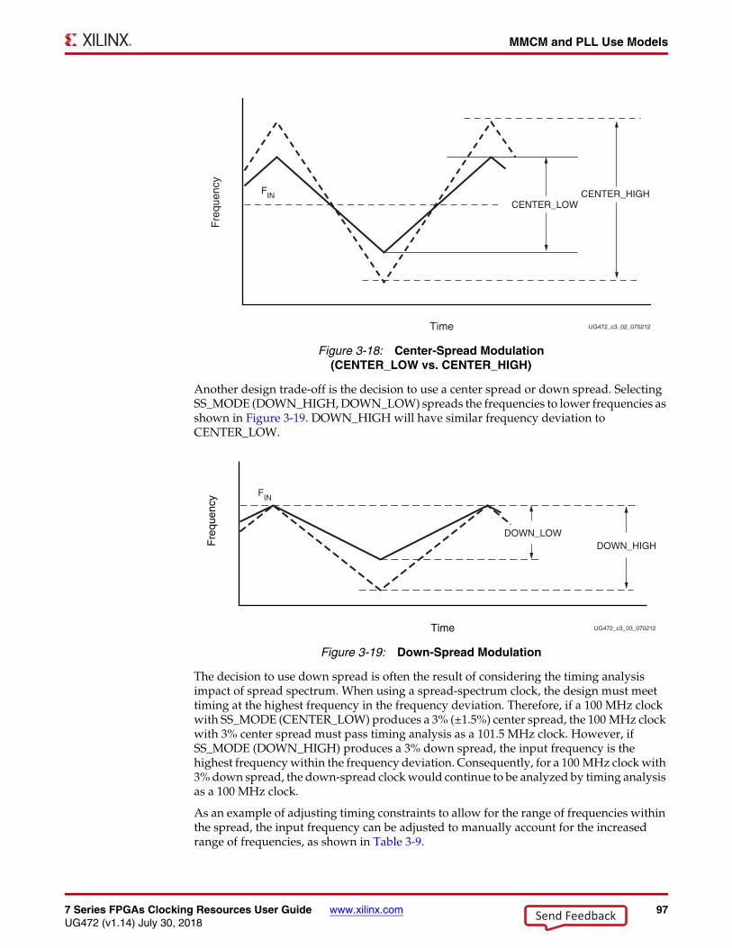
7 Series FPGAs Clocking Resources User Guide www.xilinx.com 97UG472 (v1.14) July 30, 2018
MMCM and PLL Use Models
Another design trade-off is the decision to use a center spread or down spread. Selecting SS_MODE (DOWN_HIGH, DOWN_LOW) spreads the frequencies to lower frequencies as shown in Figure 3-19. DOWN_HIGH will have similar frequency deviation to CENTER_LOW.
The decision to use down spread is often the result of considering the timing analysis impact of spread spectrum. When using a spread-spectrum clock, the design must meet timing at the highest frequency in the frequency deviation. Therefore, if a 100 MHz clock with SS_MODE (CENTER_LOW) produces a 3% (±1.5%) center spread, the 100 MHz clock with 3% center spread must pass timing analysis as a 101.5 MHz clock. However, if SS_MODE (DOWN_HIGH) produces a 3% down spread, the input frequency is the highest frequency within the frequency deviation. Consequently, for a 100 MHz clock with 3% down spread, the down-spread clock would continue to be analyzed by timing analysis as a 100 MHz clock.
As an example of adjusting timing constraints to allow for the range of frequencies within the spread, the input frequency can be adjusted to manually account for the increased range of frequencies, as shown in Table 3-9.
X-Ref Target - Figure 3-18
Figure 3-18: Center-Spread Modulation(CENTER_LOW vs. CENTER_HIGH)
X-Ref Target - Figure 3-19
Figure 3-19: Down-Spread Modulation
Fre
quen
cy
Time
CENTER_LOW
FIN CENTER_HIGH
UG472_c3_02_070212
Fre
quen
cy
Time
DOWN_LOW
FIN
DOWN_HIGH
UG472_c3_03_070212
Send Feedback
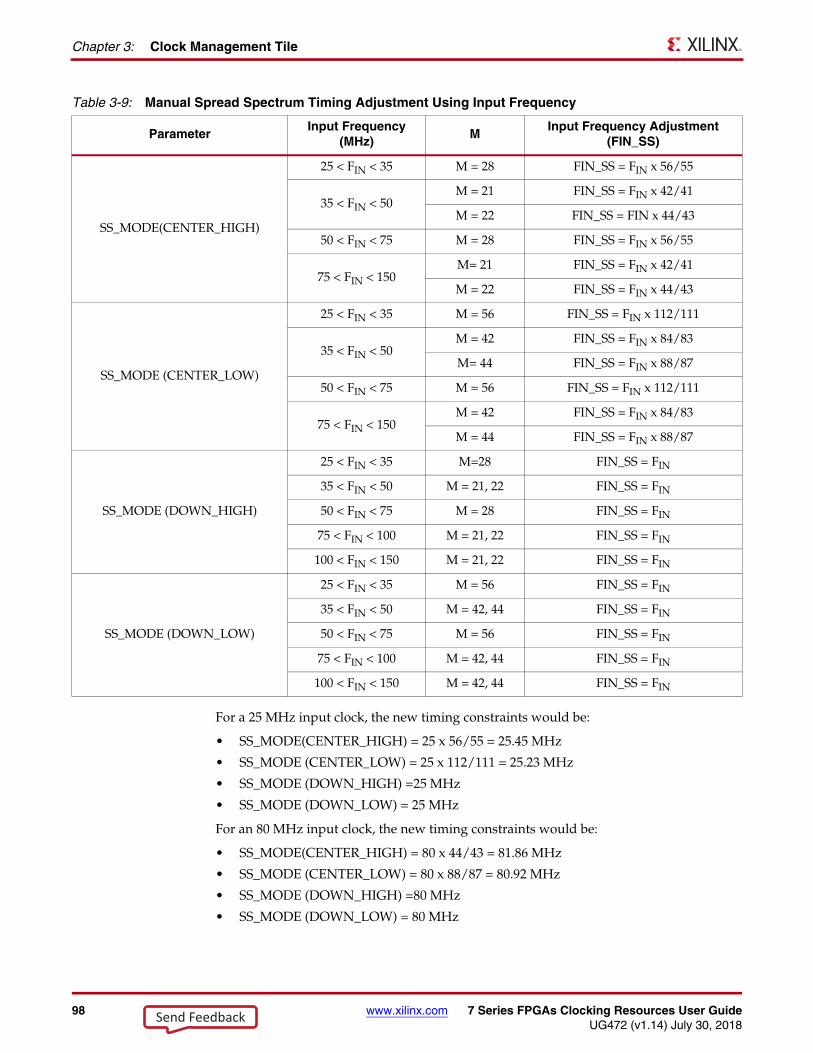
98 www.xilinx.com 7 Series FPGAs Clocking Resources User GuideUG472 (v1.14) July 30, 2018
Chapter 3: Clock Management Tile
For a 25 MHz input clock, the new timing constraints would be:
• SS_MODE(CENTER_HIGH) = 25 x 56/55 = 25.45 MHz
• SS_MODE (CENTER_LOW) = 25 x 112/111 = 25.23 MHz
• SS_MODE (DOWN_HIGH) =25 MHz
• SS_MODE (DOWN_LOW) = 25 MHz
For an 80 MHz input clock, the new timing constraints would be:
• SS_MODE(CENTER_HIGH) = 80 x 44/43 = 81.86 MHz
• SS_MODE (CENTER_LOW) = 80 x 88/87 = 80.92 MHz
• SS_MODE (DOWN_HIGH) =80 MHz
• SS_MODE (DOWN_LOW) = 80 MHz
Table 3-9: Manual Spread Spectrum Timing Adjustment Using Input Frequency
ParameterInput Frequency
(MHz)M
Input Frequency Adjustment (FIN_SS)
SS_MODE(CENTER_HIGH)
25 < FIN < 35 M = 28 FIN_SS = FIN x 56/55
35 < FIN < 50M = 21 FIN_SS = FIN x 42/41
M = 22 FIN_SS = FIN x 44/43
50 < FIN < 75 M = 28 FIN_SS = FIN x 56/55
75 < FIN < 150M= 21 FIN_SS = FIN x 42/41
M = 22 FIN_SS = FIN x 44/43
SS_MODE (CENTER_LOW)
25 < FIN < 35 M = 56 FIN_SS = FIN x 112/111
35 < FIN < 50M = 42 FIN_SS = FIN x 84/83
M= 44 FIN_SS = FIN x 88/87
50 < FIN < 75 M = 56 FIN_SS = FIN x 112/111
75 < FIN < 150M = 42 FIN_SS = FIN x 84/83
M = 44 FIN_SS = FIN x 88/87
SS_MODE (DOWN_HIGH)
25 < FIN < 35 M=28 FIN_SS = FIN
35 < FIN < 50 M = 21, 22 FIN_SS = FIN
50 < FIN < 75 M = 28 FIN_SS = FIN
75 < FIN < 100 M = 21, 22 FIN_SS = FIN
100 < FIN < 150 M = 21, 22 FIN_SS = FIN
SS_MODE (DOWN_LOW)
25 < FIN < 35 M = 56 FIN_SS = FIN
35 < FIN < 50 M = 42, 44 FIN_SS = FIN
50 < FIN < 75 M = 56 FIN_SS = FIN
75 < FIN < 100 M = 42, 44 FIN_SS = FIN
100 < FIN < 150 M = 42, 44 FIN_SS = FIN
Send Feedback
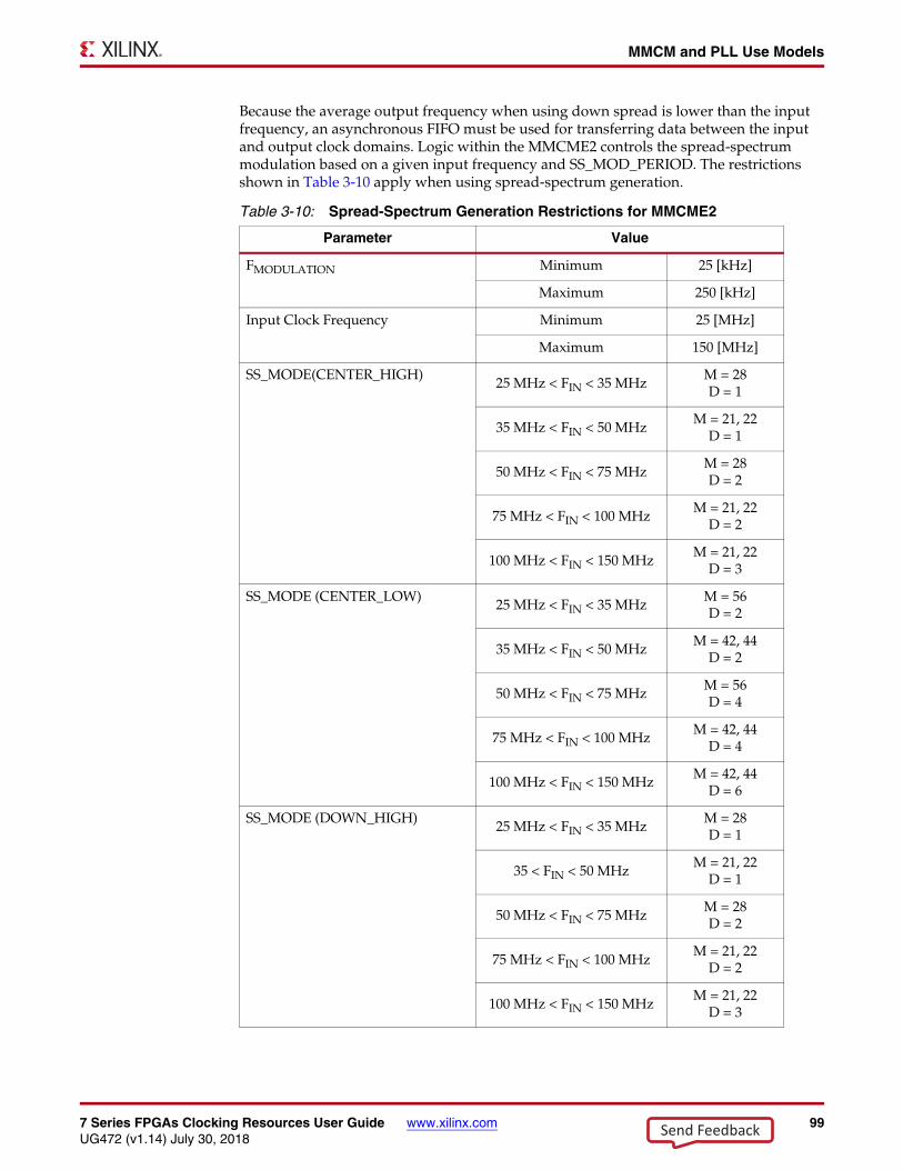
7 Series FPGAs Clocking Resources User Guide www.xilinx.com 99UG472 (v1.14) July 30, 2018
MMCM and PLL Use Models
Because the average output frequency when using down spread is lower than the input frequency, an asynchronous FIFO must be used for transferring data between the input and output clock domains. Logic within the MMCME2 controls the spread-spectrum modulation based on a given input frequency and SS_MOD_PERIOD. The restrictions shown in Table 3-10 apply when using spread-spectrum generation.
Table 3-10: Spread-Spectrum Generation Restrictions for MMCME2
Parameter Value
FMODULATION Minimum 25 [kHz]
Maximum 250 [kHz]
Input Clock Frequency Minimum 25 [MHz]
Maximum 150 [MHz]
SS_MODE(CENTER_HIGH)25 MHz < FIN < 35 MHz
M = 28D = 1
35 MHz < FIN < 50 MHzM = 21, 22
D = 1
50 MHz < FIN < 75 MHzM = 28D = 2
75 MHz < FIN < 100 MHz M = 21, 22D = 2
100 MHz < FIN < 150 MHz M = 21, 22D = 3
SS_MODE (CENTER_LOW) 25 MHz < FIN < 35 MHz M = 56D = 2
35 MHz < FIN < 50 MHz M = 42, 44D = 2
50 MHz < FIN < 75 MHz M = 56D = 4
75 MHz < FIN < 100 MHz M = 42, 44D = 4
100 MHz < FIN < 150 MHz M = 42, 44D = 6
SS_MODE (DOWN_HIGH) 25 MHz < FIN < 35 MHz M = 28D = 1
35 < FIN < 50 MHzM = 21, 22
D = 1
50 MHz < FIN < 75 MHzM = 28D = 2
75 MHz < FIN < 100 MHzM = 21, 22
D = 2
100 MHz < FIN < 150 MHzM = 21, 22
D = 3
Send Feedback
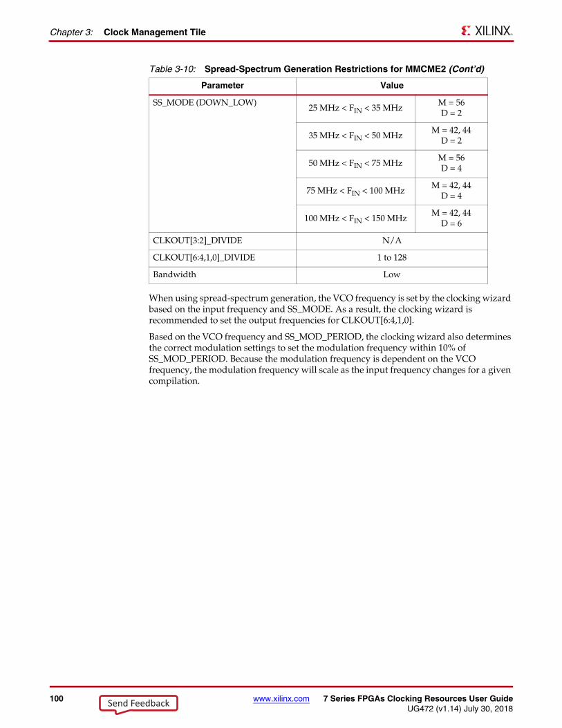
100 www.xilinx.com 7 Series FPGAs Clocking Resources User GuideUG472 (v1.14) July 30, 2018
Chapter 3: Clock Management Tile
When using spread-spectrum generation, the VCO frequency is set by the clocking wizard based on the input frequency and SS_MODE. As a result, the clocking wizard is recommended to set the output frequencies for CLKOUT[6:4,1,0].
Based on the VCO frequency and SS_MOD_PERIOD, the clocking wizard also determines the correct modulation settings to set the modulation frequency within 10% of SS_MOD_PERIOD. Because the modulation frequency is dependent on the VCO frequency, the modulation frequency will scale as the input frequency changes for a given compilation.
SS_MODE (DOWN_LOW)25 MHz < FIN < 35 MHz
M = 56D = 2
35 MHz < FIN < 50 MHzM = 42, 44
D = 2
50 MHz < FIN < 75 MHzM = 56D = 4
75 MHz < FIN < 100 MHzM = 42, 44
D = 4
100 MHz < FIN < 150 MHzM = 42, 44
D = 6
CLKOUT[3:2]_DIVIDE N/A
CLKOUT[6:4,1,0]_DIVIDE 1 to 128
Bandwidth Low
Table 3-10: Spread-Spectrum Generation Restrictions for MMCME2 (Cont’d)
Parameter Value
Send Feedback
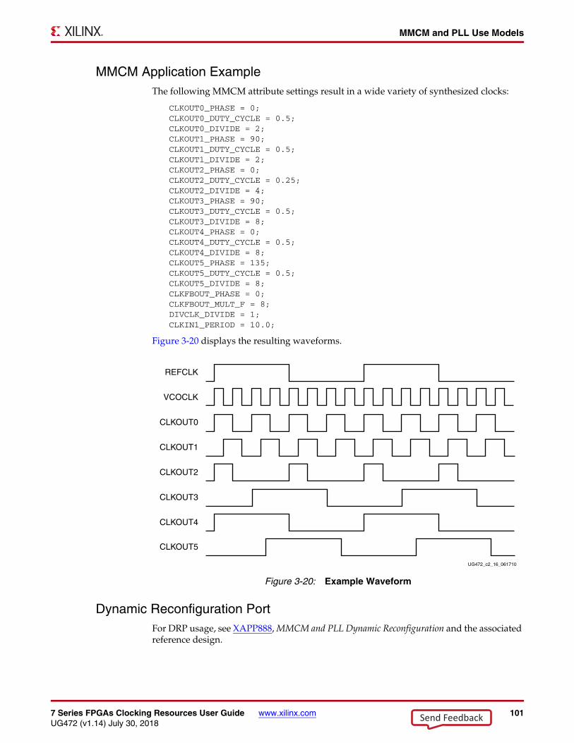
7 Series FPGAs Clocking Resources User Guide www.xilinx.com 101UG472 (v1.14) July 30, 2018
MMCM and PLL Use Models
MMCM Application ExampleThe following MMCM attribute settings result in a wide variety of synthesized clocks:
CLKOUT0_PHASE = 0;CLKOUT0_DUTY_CYCLE = 0.5;CLKOUT0_DIVIDE = 2;CLKOUT1_PHASE = 90;CLKOUT1_DUTY_CYCLE = 0.5;CLKOUT1_DIVIDE = 2;CLKOUT2_PHASE = 0;CLKOUT2_DUTY_CYCLE = 0.25;CLKOUT2_DIVIDE = 4;CLKOUT3_PHASE = 90;CLKOUT3_DUTY_CYCLE = 0.5;CLKOUT3_DIVIDE = 8;CLKOUT4_PHASE = 0;CLKOUT4_DUTY_CYCLE = 0.5;CLKOUT4_DIVIDE = 8;CLKOUT5_PHASE = 135;CLKOUT5_DUTY_CYCLE = 0.5;CLKOUT5_DIVIDE = 8;CLKFBOUT_PHASE = 0;CLKFBOUT_MULT_F = 8;DIVCLK_DIVIDE = 1;CLKIN1_PERIOD = 10.0;
Figure 3-20 displays the resulting waveforms.
Dynamic Reconfiguration PortFor DRP usage, see XAPP888, MMCM and PLL Dynamic Reconfiguration and the associated reference design.
X-Ref Target - Figure 3-20
Figure 3-20: Example Waveform
REFCLK
VCOCLK
CLKOUT0
CLKOUT1
CLKOUT2
CLKOUT3
CLKOUT4
CLKOUT5
UG472_c2_16_061710
Send Feedback
102 www.xilinx.com 7 Series FPGAs Clocking Resources User GuideUG472 (v1.14) July 30, 2018
Chapter 3: Clock Management Tile
VHDL and Verilog Templates and the Clocking WizardThe VHDL and Verilog code for all clocking resource primitives and the ISE or Vivado design tools language templates are available in the Libraries Guide.
The Clocking Wizard helps to correctly set up the 7 series MMCM and PLL resources. Additionally, the Clocking Wizard reports the jitter and supports phase and frequency synthesis.
Send Feedback
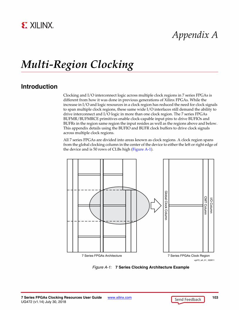
7 Series FPGAs Clocking Resources User Guide www.xilinx.com 103UG472 (v1.14) July 30, 2018
Appendix A
Multi-Region Clocking
IntroductionClocking and I/O interconnect logic across multiple clock regions in 7 series FPGAs is different from how it was done in previous generations of Xilinx FPGAs. While the increase in I/O and logic resources in a clock region has reduced the need for clock signals to span multiple clock regions, these same wide I/O interfaces still demand the ability to drive interconnect and I/O logic in more than one clock region. The 7 series FPGAs BUFMR/BUFMRCE primitives enable clock-capable input pins to drive BUFIOs and BUFRs in the region same region the input resides as well as the regions above and below. This appendix details using the BUFIO and BUFR clock buffers to drive clock signals across multiple clock regions.
All 7 series FPGAs are divided into areas known as clock regions. A clock region spans from the global clocking column in the center of the device to either the left or right edge of the device and is 50 rows of CLBs high (Figure A-1).X-Ref Target - Figure A-1
Figure A-1: 7 Series Clocking Architecture Example
7 Series FPGAs Architecture 7 Series FPGAs Clock Region
Global C
lock Colum
n
CM
T C
olumn
I/O C
olumn
ug472_aA_01_ 022811
Send Feedback
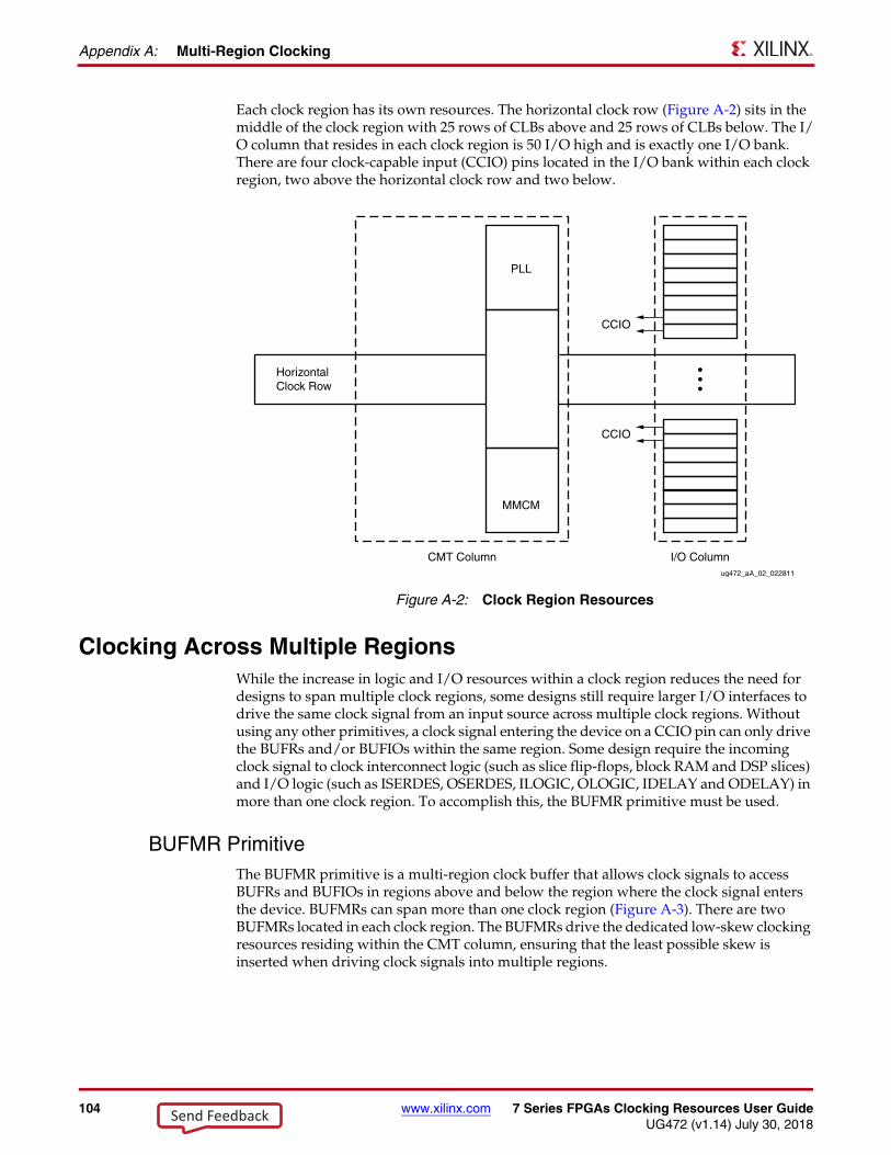
104 www.xilinx.com 7 Series FPGAs Clocking Resources User GuideUG472 (v1.14) July 30, 2018
Appendix A: Multi-Region Clocking
Each clock region has its own resources. The horizontal clock row (Figure A-2) sits in the middle of the clock region with 25 rows of CLBs above and 25 rows of CLBs below. The I/O column that resides in each clock region is 50 I/O high and is exactly one I/O bank. There are four clock-capable input (CCIO) pins located in the I/O bank within each clock region, two above the horizontal clock row and two below.
Clocking Across Multiple RegionsWhile the increase in logic and I/O resources within a clock region reduces the need for designs to span multiple clock regions, some designs still require larger I/O interfaces to drive the same clock signal from an input source across multiple clock regions. Without using any other primitives, a clock signal entering the device on a CCIO pin can only drive the BUFRs and/or BUFIOs within the same region. Some design require the incoming clock signal to clock interconnect logic (such as slice flip-flops, block RAM and DSP slices) and I/O logic (such as ISERDES, OSERDES, ILOGIC, OLOGIC, IDELAY and ODELAY) in more than one clock region. To accomplish this, the BUFMR primitive must be used.
BUFMR PrimitiveThe BUFMR primitive is a multi-region clock buffer that allows clock signals to access BUFRs and BUFIOs in regions above and below the region where the clock signal enters the device. BUFMRs can span more than one clock region (Figure A-3). There are two BUFMRs located in each clock region. The BUFMRs drive the dedicated low-skew clocking resources residing within the CMT column, ensuring that the least possible skew is inserted when driving clock signals into multiple regions.
X-Ref Target - Figure A-2
Figure A-2: Clock Region Resources
HorizontalClock Row
CMT Column
PLL
MMCM
CCIO
CCIO
I/O Columnug472_aA_02_022811
Send Feedback
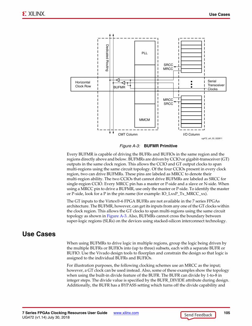
7 Series FPGAs Clocking Resources User Guide www.xilinx.com 105UG472 (v1.14) July 30, 2018
Use Cases
Every BUFMR is capable of driving the BUFRs and BUFIOs in the same region and the regions directly above and below. BUFMRs are driven by CCIO or gigabit-transceiver (GT) outputs in the same clock region. This allows the CCIO and GT output clocks to span multi-regions using the same circuit topology. Of the four CCIOs present in every clock region, two can drive BUFMRs. These pins are labeled as MRCC to denote their multi-region ability. The two CCIOs that cannot drive BUFMRs are labeled as SRCC for single-region CCIO. Every MRCC pin has a master or P-side and a slave or N-side. When using a MRCC pin to drive a BUFMR, use only the master or P-side. To identify the master or P-side, look for a P in the pin name (for example: IO_LxxP_Tx_MRCC_xx).
The GT inputs to the Virtex®-6 FPGA BUFRs are not available in the 7 series FPGAs architecture. The BUFMR, however, can get its inputs from any one of the GT clocks within the clock region. This allows the GT clocks to span multi-regions using the same circuit topology as shown in Figure A-3. Also, BUFMRs cannot cross the boundary between super-logic regions (SLRs) on the devices using stacked-silicon interconnect technology.
Use CasesWhen using BUFMRs to drive logic in multiple regions, group the logic being driven by the multiple BUFRs or BUFIOs into (up to three) subsets, each with a separate BUFR or BUFIO. Use the Vivado design tools to floorplan and constrain the design so that logic is assigned to the individual BUFRs and BUFIOs.
For illustration purposes, the following clocking schemes use an MRCC as the input; however, a GT clock can be used instead. Also, some of these examples show the topology when using the built-in divide feature of the BUFR. The BUFR can divide by 1-to-8 in integer steps. The divide value is specified by the BUFR_DIVIDE attribute during design. Additionally, the BUFR has a BYPASS setting which turns off the divide capability and
X-Ref Target - Figure A-3
Figure A-3: BUFMR Primitive
HorizontalClock Row
CMT Column
PLL
MMCM
MRCCSRCC
SRCCMRCC
I/O Columnug472_aA_03_022811
Serial TransceiverClocksBUFMR
Dedicated R
outing
Send Feedback
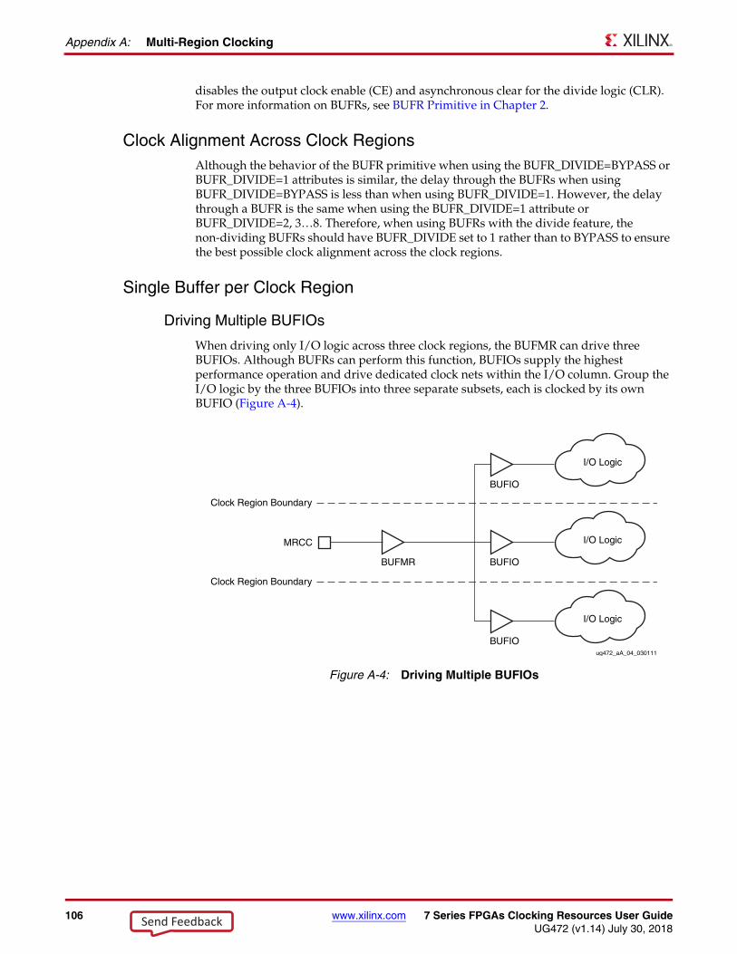
106 www.xilinx.com 7 Series FPGAs Clocking Resources User GuideUG472 (v1.14) July 30, 2018
Appendix A: Multi-Region Clocking
disables the output clock enable (CE) and asynchronous clear for the divide logic (CLR). For more information on BUFRs, see BUFR Primitive in Chapter 2.
Clock Alignment Across Clock RegionsAlthough the behavior of the BUFR primitive when using the BUFR_DIVIDE=BYPASS or BUFR_DIVIDE=1 attributes is similar, the delay through the BUFRs when using BUFR_DIVIDE=BYPASS is less than when using BUFR_DIVIDE=1. However, the delay through a BUFR is the same when using the BUFR_DIVIDE=1 attribute or BUFR_DIVIDE=2, 3…8. Therefore, when using BUFRs with the divide feature, the non-dividing BUFRs should have BUFR_DIVIDE set to 1 rather than to BYPASS to ensure the best possible clock alignment across the clock regions.
Single Buffer per Clock Region
Driving Multiple BUFIOs
When driving only I/O logic across three clock regions, the BUFMR can drive three BUFIOs. Although BUFRs can perform this function, BUFIOs supply the highest performance operation and drive dedicated clock nets within the I/O column. Group the I/O logic by the three BUFIOs into three separate subsets, each is clocked by its own BUFIO (Figure A-4).X-Ref Target - Figure A-4
Figure A-4: Driving Multiple BUFIOs
BUFMR
MRCC
BUFIO
I/O Logic
BUFIO
I/O Logic
BUFIO
I/O Logic
ug472_aA_04_030111
Clock Region Boundary
Clock Region Boundary
Send Feedback
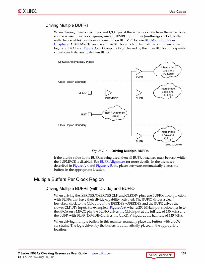
7 Series FPGAs Clocking Resources User Guide www.xilinx.com 107UG472 (v1.14) July 30, 2018
Use Cases
Driving Multiple BUFRs
When driving interconnect logic and I/O logic at the same clock rate from the same clock source across three clock regions, use a BUFMRCE primitive (multi-region clock buffer with clock enable). For more information on BUFMRCEs, see BUFMR Primitive in Chapter 2. A BUFMRCE can drive three BUFRs which, in turn, drive both interconnect logic and I/O logic (Figure A-5). Group the logic clocked by the three BUFRs into separate subsets, each driven by its own BUFR.
If the divide value in the BUFR is being used, then all BUFR instances must be reset while the BUFMRCE is disabled. See BUFR Alignment for more details. In the use cases described in Figure A-4 and Figure A-5, the placer software automatically places the buffers in the appropriate location.
Multiple Buffers Per Clock Region
Driving Multiple BUFRs (with Divide) and BUFIO
When driving the ISERDES/OSERDES CLK and CLKDIV pins, use BUFIOs in conjunction with BUFRs that have their divide capability activated. The BUFIO drives a clean, low-skew clock to the CLK port of the ISERDES/OSERDES and the BUFR drives the slower CLKDIV input. For example in Figure A-6, when a 250 MHz input clock comes in to the FPGA on a MRCC pin, the BUFIO drives the CLK input at the full rate of 250 MHz and the BUFR with BUFR_DIVIDE=2 drives the CLKDIV inputs at the half rate of 125 MHz.
When driving multiple buffers in this manner, manually place the buffers with a LOC constraint. The logic driven by the buffers is automatically placed in the appropriate location.
X-Ref Target - Figure A-5
Figure A-5: Driving Multiple BUFRs
BUFMRCE
MRCC
BUFR
BUFR Alignment Circuit
BUFR
InterconnectLogic andI/O Logic
InterconnectLogic and I/O Logic
InterconnectLogic andI/O Logic
BUFR
RST
ug472_aA_05_030111
Clock Region Boundary
Software Automatically Places
Clock Region Boundary
Send Feedback
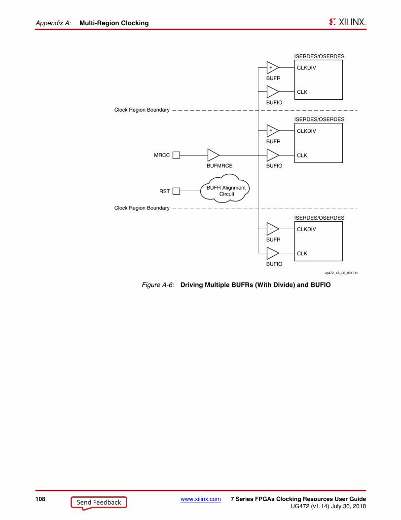
108 www.xilinx.com 7 Series FPGAs Clocking Resources User GuideUG472 (v1.14) July 30, 2018
Appendix A: Multi-Region Clocking
X-Ref Target - Figure A-6
Figure A-6: Driving Multiple BUFRs (With Divide) and BUFIO
BUFMRCE
MRCC
BUFIO
BUFR
BUFR Alignment CircuitRST
Clock Region BoundaryBUFIO
BUFR
CLK
CLKDIV
CLK
CLKDIV
BUFIO
BUFR
Clock Region Boundary
CLK
CLKDIV
ISERDES/OSERDES
ISERDES/OSERDES
ISERDES/OSERDES
÷
÷
÷
ug472_aA_06_051311
Send Feedback
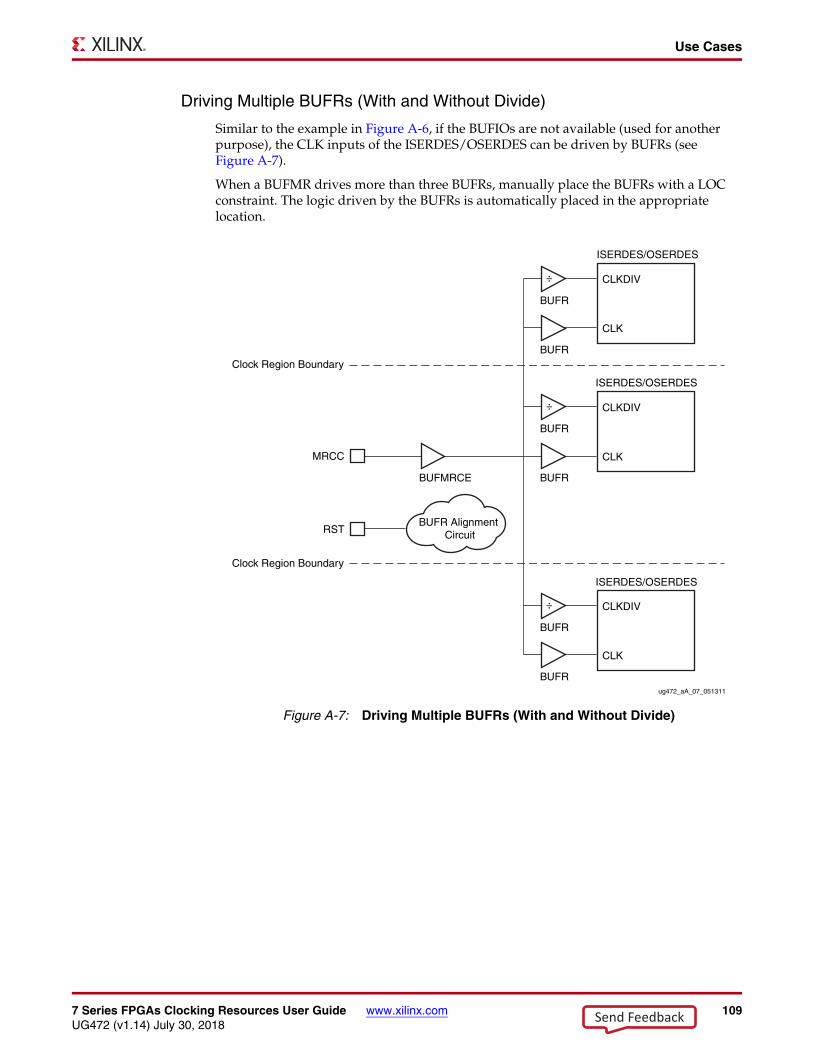
7 Series FPGAs Clocking Resources User Guide www.xilinx.com 109UG472 (v1.14) July 30, 2018
Use Cases
Driving Multiple BUFRs (With and Without Divide)
Similar to the example in Figure A-6, if the BUFIOs are not available (used for another purpose), the CLK inputs of the ISERDES/OSERDES can be driven by BUFRs (see Figure A-7).
When a BUFMR drives more than three BUFRs, manually place the BUFRs with a LOC constraint. The logic driven by the BUFRs is automatically placed in the appropriate location.X-Ref Target - Figure A-7
Figure A-7: Driving Multiple BUFRs (With and Without Divide)
BUFMRCE
MRCC
BUFR
BUFR
BUFR Alignment CircuitRST
Clock Region BoundaryBUFR
BUFR
CLK
CLKDIV
CLK
CLKDIV
ISERDES/OSERDES
ISERDES/OSERDES
ISERDES/OSERDES
BUFR
BUFR
Clock Region Boundary
CLK
CLKDIV
÷
÷
÷
ug472_aA_07_051311
Send Feedback
110 www.xilinx.com 7 Series FPGAs Clocking Resources User GuideUG472 (v1.14) July 30, 2018
Appendix A: Multi-Region Clocking
BUFR AlignmentWhen using the built in divide capability of the BUFR (shown in Figure A-6 and Figure A-7, the clock must be stopped at the BUFMR and reset signals applied to the BUFRs, to align the BUFR divide counters across the multiple clock regions. This will require using the BUFMRCE primitive, which allows you to disable the output of the BUFMR during the reset. To successfully align the BUFRs in adjacent regions, the following procedure must be followed:
• Connect the clock enable to the CE port of the BUFMRCE
• Hold the CE pin of the BUFMRCE in its inactive state to disable the output of the BUFMRCE
• Reset all BUFRs by applying a reset signal to the CLR pin of the BUFR
• Re-enable the BUFMRCE after the BUFR reset/CLR signal is applied
• Release the reset/CLR signal on the BUFRs. All BUFRs must be released in the same clock cycle to ensure phase alignment of all the BUFR output clocks.
To turn off clocks during circuit operations, that is after the reset/CLR signal to the BUFRs is deasserted, disable the BUFMRCE using its CE pin. This ensures that the BUFRs continue to be aligned when the clock signal is reinstated. The BUFMRCEs CE pin should be asserted for a minimum of one input clock cycle.
Send Feedback
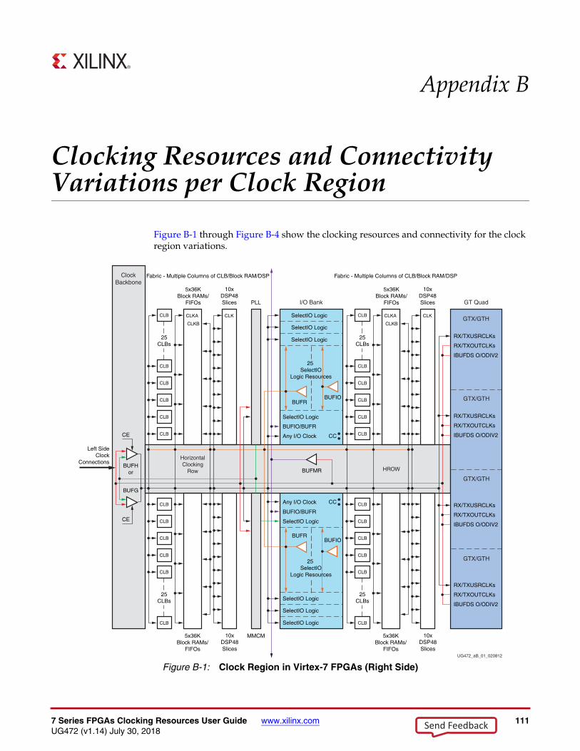
7 Series FPGAs Clocking Resources User Guide www.xilinx.com 111UG472 (v1.14) July 30, 2018
Appendix B
Clocking Resources and Connectivity Variations per Clock Region
Figure B-1 through Figure B-4 show the clocking resources and connectivity for the clock region variations.
X-Ref Target - Figure B-1
Figure B-1: Clock Region in Virtex-7 FPGAs (Right Side)UG472_aB_01_020812
ClockBackbone
BUFHor
CE
Fabric - Multiple Columns of CLB/Block RAM/DSP
BUFG
BUFMR
Left SideClock
Connections
CE
PLL
CLK
10xDSP48Slices
CLKA
CLKB
5x36KBlock RAMs/
FIFOs
MMCM10xDSP48Slices
5x36KBlock RAMs/
FIFOs
CLB
CLB
CLB
CLB
CLB
CLB
CLB
CLB
CLB
CLB
CLB
CLB
25CLBs
25CLBs
CLK
10xDSP48Slices
CLKA
CLKB
5x36KBlock RAMs/
FIFOs
10xDSP48Slices
5x36KBlock RAMs/
FIFOs
CLB
CLB
CLB
CLB
CLB
CLB
CLB
CLB
CLB
CLB
CLB
CLB
25CLBs
25CLBs
Fabric - Multiple Columns of CLB/Block RAM/DSP
I/O Bank
SelectIO Logic
25 SelectIO
Logic Resources
SelectIO Logic
SelectIO Logic
SelectIO Logic
SelectIO Logic
BUFIO/BUFR
BUFIO/BUFR
Any I/O Clock
Any I/O Clock
SelectIO Logic
SelectIO Logic
SelectIO Logic
CC
CC
BUFRBUFIO
BUFRBUFIO
GT Quad
GTX/GTH
RX/TXUSRCLKs
RX/TXOUTCLKs
IBUFDS O/ODIV2
GTX/GTH
RX/TXUSRCLKs
RX/TXOUTCLKs
IBUFDS O/ODIV2
GTX/GTH
RX/TXUSRCLKs
RX/TXOUTCLKs
IBUFDS O/ODIV2
GTX/GTH
RX/TXUSRCLKs
RX/TXOUTCLKs
IBUFDS O/ODIV2
HROW
HorizontalClocking
Row
25 SelectIO
Logic Resources
Send Feedback
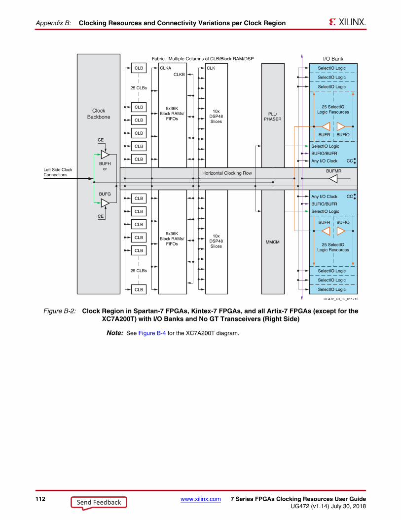
112 www.xilinx.com 7 Series FPGAs Clocking Resources User GuideUG472 (v1.14) July 30, 2018
Appendix B: Clocking Resources and Connectivity Variations per Clock Region
Note: See Figure B-4 for the XC7A200T diagram.
X-Ref Target - Figure B-2
Figure B-2: Clock Region in Spartan-7 FPGAs, Kintex-7 FPGAs, and all Artix-7 FPGAs (except for the XC7A200T) with I/O Banks and No GT Transceivers (Right Side)
UG472_aB_02_011713
ClockBackbone
I/O Bank
SelectIO Logic
Horizontal Clocking Row
BUFHor
CE
CLB
CLB
CLB
CLB
CLB
CLB
CLB
CLB
CLB
CLB
CLB
CLB
Fabric - Multiple Columns of CLB/Block RAM/DSP
CLKA
CLKB
5x36KBlock RAMs/
FIFOs
5x36KBlock RAMs/
FIFOs
25 CLBs
25 SelectIOLogic Resources
BUFG
CE
CLK
10xDSP48Slices
PLL/PHASER
10xDSP48Slices
MMCM
SelectIO Logic
SelectIO Logic
SelectIO Logic
SelectIO Logic
BUFIO/BUFR
BUFIO/BUFR
Any I/O Clock
Any I/O Clock
SelectIO Logic
SelectIO Logic
SelectIO Logic
25 SelectIOLogic Resources
25 CLBs
CC
CC
BUFR
BUFMR
BUFIO
BUFR BUFIO
Left Side ClockConnections
Send Feedback
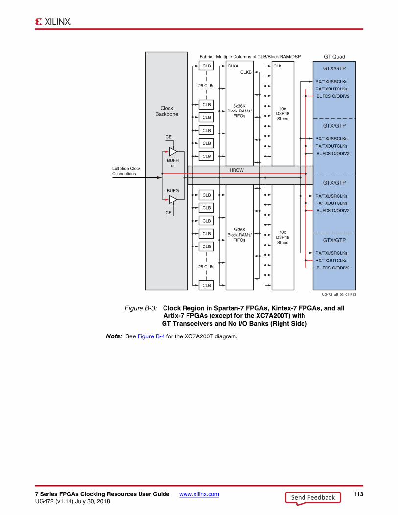
7 Series FPGAs Clocking Resources User Guide www.xilinx.com 113UG472 (v1.14) July 30, 2018
Note: See Figure B-4 for the XC7A200T diagram.
X-Ref Target - Figure B-3
Figure B-3: Clock Region in Spartan-7 FPGAs, Kintex-7 FPGAs, and all Artix-7 FPGAs (except for the XC7A200T) with GT Transceivers and No I/O Banks (Right Side)
UG472_aB_03_011713
ClockBackbone
GT Quad
GTX/GTP
RX/TXUSRCLKs
RX/TXOUTCLKs
IBUFDS O/ODIV2
GTX/GTP
RX/TXUSRCLKs
RX/TXOUTCLKs
IBUFDS O/ODIV2
HROW
BUFHor
CE
CLB
CLB
CLB
CLB
CLB
CLB
CLB
CLB
CLB
CLB
CLB
CLB
Fabric - Multiple Columns of CLB/Block RAM/DSP
CLKA
CLKB
5x36KBlock RAMs/
FIFOs
5x36KBlock RAMs/
FIFOs
25 CLBs
BUFG
Left Side ClockConnections
CE
CLK
10xDSP48Slices
10xDSP48Slices
GTX/GTP
RX/TXUSRCLKs
RX/TXOUTCLKs
IBUFDS O/ODIV2
GTX/GTP
RX/TXUSRCLKs
RX/TXOUTCLKs
IBUFDS O/ODIV225 CLBs
Send Feedback
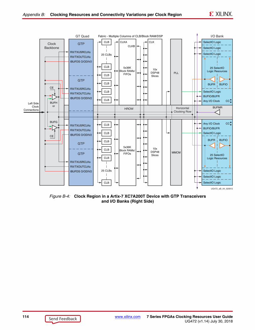
114 www.xilinx.com 7 Series FPGAs Clocking Resources User GuideUG472 (v1.14) July 30, 2018
Appendix B: Clocking Resources and Connectivity Variations per Clock Region
X-Ref Target - Figure B-4
Figure B-4: Clock Region in a Artix-7 XC7A200T Device with GTP Transceivers and I/O Banks (Right Side)
UG472_aB_04_020812
ClockBackbone
I/O Bank
SelectIO Logic
HROW HorizontalClocking Row
BUFHor
CE
CLB
CLB
CLB
CLB
CLB
CLB
CLB
CLB
CLB
CLB
CLB
CLB
Fabric - Multiple Columns of CLB/Block RAM/DSP
CLKA
CLKB
5x36KBlock RAMs/
FIFOs
5x36KBlock RAMs/
FIFOs
25 CLBs
25 SelectIOLogic Resources
BUFG
Left SideClock
Connections
CE
CLK
10xDSP48Slices
PLL
10xDSP48Slices
MMCM
SelectIO Logic
SelectIO Logic
SelectIO Logic
SelectIO Logic
BUFIO/BUFR
BUFIO/BUFR
Any I/O Clock
Any I/O Clock
SelectIO Logic
SelectIO Logic
SelectIO Logic
25 SelectIOLogic Resources
25 CLBs
CC
CC
BUFR
BUFMR
BUFIO
BUFR BUFIO
GT Quad
GTP
RX/TXUSRCLKs
RX/TXOUTCLKs
IBUFDS O/ODIV2
GTP
RX/TXUSRCLKs
RX/TXOUTCLKs
IBUFDS O/ODIV2
GTP
RX/TXUSRCLKs
RX/TXOUTCLKs
IBUFDS O/ODIV2
GTP
RX/TXUSRCLKs
RX/TXOUTCLKs
IBUFDS O/ODIV2
Send Feedback