Embed Size (px)
Citation preview
LogiCORE IP Ten Gigabit Ethernet PCS/PMA v2.1User Guide
UG692 March 1, 2011
LogiCORE 10GBASE-R User Guide www.xilinx.com UG692 March 1, 2011
Xilinx is providing this product documentation, hereinafter “Information,” to you “AS IS” with no warranty of any kind, express or implied. Xilinx makes no representation that the Information, or any particular implementation thereof, is free from any claims of infringement. You are responsible for obtaining any rights you may require for any implementation based on the Information. All specifications are subject to change without notice.
XILINX EXPRESSLY DISCLAIMS ANY WARRANTY WHATSOEVER WITH RESPECT TO THE ADEQUACY OF THE INFORMATION OR ANY IMPLEMENTATION BASED THEREON, INCLUDING BUT NOT LIMITED TO ANY WARRANTIES OR REPRESENTATIONS THAT THIS IMPLEMENTATION IS FREE FROM CLAIMS OF INFRINGEMENT AND ANY IMPLIED WARRANTIES OF MERCHANTABILITY OR FITNESS FOR A PARTICULAR PURPOSE.
Except as stated herein, none of the Information may be copied, reproduced, distributed, republished, downloaded, displayed, posted, or transmitted in any form or by any means including, but not limited to, electronic, mechanical, photocopying, recording, or otherwise, without the prior written consent of Xilinx.
© Copyright 2009- 2011 Xilinx, Inc. XILINX, the Xilinx logo, Artix, ISE, Kintex, Spartan, Virtex, and other designated brands included herein are trademarks of Xilinx in the United States and other countries. PCI, PCIe and PCI Express are trademarks of PCI-SIG and used under license. All other trademarks are the property of their respective owners.
Revision HistoryThe table shows the revision history for this document.
Date Version Revision
12/02/09 1.1 Initial Xilinx release
4/19/10 1.2 Update to core version 1.2; update Xilinx tools to 12.1.
3/01/11 2.1 Update to core version 2.1; update Xilinx tools to 13.1. Added Virtex®-7 and Kintex™-7 FPGAs support.
Table of Contents
Revision History . . . . . . . . . . . . . . . . . . . . . . . . . . . . . . . . . . . . . . . . . . . . . . . . . . . . . . . . . . . . . 2
Preface: About This GuideGuide Contents . . . . . . . . . . . . . . . . . . . . . . . . . . . . . . . . . . . . . . . . . . . . . . . . . . . . . . . . . . . . . 13Additional Resources . . . . . . . . . . . . . . . . . . . . . . . . . . . . . . . . . . . . . . . . . . . . . . . . . . . . . . . 14Conventions . . . . . . . . . . . . . . . . . . . . . . . . . . . . . . . . . . . . . . . . . . . . . . . . . . . . . . . . . . . . . . . . 14
Typographical . . . . . . . . . . . . . . . . . . . . . . . . . . . . . . . . . . . . . . . . . . . . . . . . . . . . . . . . . . . . 14Online Document . . . . . . . . . . . . . . . . . . . . . . . . . . . . . . . . . . . . . . . . . . . . . . . . . . . . . . . . . 15List of Acronyms . . . . . . . . . . . . . . . . . . . . . . . . . . . . . . . . . . . . . . . . . . . . . . . . . . . . . . . . . 15
Chapter 1: IntroductionSystem Requirements . . . . . . . . . . . . . . . . . . . . . . . . . . . . . . . . . . . . . . . . . . . . . . . . . . . . . . . 17About the Core . . . . . . . . . . . . . . . . . . . . . . . . . . . . . . . . . . . . . . . . . . . . . . . . . . . . . . . . . . . . . . 17Recommended Design Experience . . . . . . . . . . . . . . . . . . . . . . . . . . . . . . . . . . . . . . . . . . . 17Additional Core Resources . . . . . . . . . . . . . . . . . . . . . . . . . . . . . . . . . . . . . . . . . . . . . . . . . . 18
Documentation . . . . . . . . . . . . . . . . . . . . . . . . . . . . . . . . . . . . . . . . . . . . . . . . . . . . . . . . . . . 1810GBASE-R Technology . . . . . . . . . . . . . . . . . . . . . . . . . . . . . . . . . . . . . . . . . . . . . . . . . . . 18Ethernet Specifications . . . . . . . . . . . . . . . . . . . . . . . . . . . . . . . . . . . . . . . . . . . . . . . . . . . . 18Other Information . . . . . . . . . . . . . . . . . . . . . . . . . . . . . . . . . . . . . . . . . . . . . . . . . . . . . . . . 18
Technical Support. . . . . . . . . . . . . . . . . . . . . . . . . . . . . . . . . . . . . . . . . . . . . . . . . . . . . . . . . . . 18Feedback. . . . . . . . . . . . . . . . . . . . . . . . . . . . . . . . . . . . . . . . . . . . . . . . . . . . . . . . . . . . . . . . . . . . 19
Core . . . . . . . . . . . . . . . . . . . . . . . . . . . . . . . . . . . . . . . . . . . . . . . . . . . . . . . . . . . . . . . . . . . . 19Document . . . . . . . . . . . . . . . . . . . . . . . . . . . . . . . . . . . . . . . . . . . . . . . . . . . . . . . . . . . . . . . 19
Chapter 2: Licensing the Core
Chapter 3: Core ArchitectureSystem Overview . . . . . . . . . . . . . . . . . . . . . . . . . . . . . . . . . . . . . . . . . . . . . . . . . . . . . . . . . . . 23Functional Description . . . . . . . . . . . . . . . . . . . . . . . . . . . . . . . . . . . . . . . . . . . . . . . . . . . . . . 23
Applications . . . . . . . . . . . . . . . . . . . . . . . . . . . . . . . . . . . . . . . . . . . . . . . . . . . . . . . . . . . . . 25Core Interfaces and Modules . . . . . . . . . . . . . . . . . . . . . . . . . . . . . . . . . . . . . . . . . . . . . . . . 26
Client-Side Interface . . . . . . . . . . . . . . . . . . . . . . . . . . . . . . . . . . . . . . . . . . . . . . . . . . . . . . 26Transceiver Data Interface - Virtex-7/Kintex-7 FPGA GTX Transceiver . . . . . . . . . . 27Transceiver Data Interface - Virtex-6 FPGA GTH Transceiver . . . . . . . . . . . . . . . . . . . 27Optical Module Interface . . . . . . . . . . . . . . . . . . . . . . . . . . . . . . . . . . . . . . . . . . . . . . . . . . 28MDIO Interface . . . . . . . . . . . . . . . . . . . . . . . . . . . . . . . . . . . . . . . . . . . . . . . . . . . . . . . . . . . 28Configuration and Status Signals . . . . . . . . . . . . . . . . . . . . . . . . . . . . . . . . . . . . . . . . . . . 28Clocking and Reset Signals - Virtex-7/Kintex-7 FPGAs . . . . . . . . . . . . . . . . . . . . . . . . 29Clocking and Reset Signals - Virtex-6 FPGAs . . . . . . . . . . . . . . . . . . . . . . . . . . . . . . . . . 29Transceiver Management Interface . . . . . . . . . . . . . . . . . . . . . . . . . . . . . . . . . . . . . . . . . . 30
Miscellaneous Signals - Virtex-7/Kintex-7 FPGAs . . . . . . . . . . . . . . . . . . . . . . . . . . . . 30
LogiCORE 10GBASE-R User Guide www.xilinx.com 3UG692 March 1, 2011
Chapter 4: Customizing and Generating the CoreGUI Interface . . . . . . . . . . . . . . . . . . . . . . . . . . . . . . . . . . . . . . . . . . . . . . . . . . . . . . . . . . . . . . . 31
Component Name . . . . . . . . . . . . . . . . . . . . . . . . . . . . . . . . . . . . . . . . . . . . . . . . . . . . . . . . 32MDIO Management . . . . . . . . . . . . . . . . . . . . . . . . . . . . . . . . . . . . . . . . . . . . . . . . . . . . . . . 32
Parameter Values in the XCO File . . . . . . . . . . . . . . . . . . . . . . . . . . . . . . . . . . . . . . . . . . . 32Output Generation . . . . . . . . . . . . . . . . . . . . . . . . . . . . . . . . . . . . . . . . . . . . . . . . . . . . . . . . . . 32
Chapter 5: Designing with the CoreGeneral Design Guidelines . . . . . . . . . . . . . . . . . . . . . . . . . . . . . . . . . . . . . . . . . . . . . . . . . 33
Use the Example Design as a Starting Point . . . . . . . . . . . . . . . . . . . . . . . . . . . . . . . . . . 33Know the Degree of Difficulty . . . . . . . . . . . . . . . . . . . . . . . . . . . . . . . . . . . . . . . . . . . . . . 33Keep It Registered . . . . . . . . . . . . . . . . . . . . . . . . . . . . . . . . . . . . . . . . . . . . . . . . . . . . . . . . 33Recognize Timing Critical Signals . . . . . . . . . . . . . . . . . . . . . . . . . . . . . . . . . . . . . . . . . . . 34Use Supported Design Flows . . . . . . . . . . . . . . . . . . . . . . . . . . . . . . . . . . . . . . . . . . . . . . . 34Make Only Allowed Modifications . . . . . . . . . . . . . . . . . . . . . . . . . . . . . . . . . . . . . . . . . . 34
Chapter 6: Interfacing to the CoreData Interface: Internal Interfaces . . . . . . . . . . . . . . . . . . . . . . . . . . . . . . . . . . . . . . . . . . . 35
Internal 64-bit SDR Client-side Interface . . . . . . . . . . . . . . . . . . . . . . . . . . . . . . . . . . . . . 35Definitions of Control Characters . . . . . . . . . . . . . . . . . . . . . . . . . . . . . . . . . . . . . . . . . . . 36
Interfacing to the Transmit Client Interface . . . . . . . . . . . . . . . . . . . . . . . . . . . . . . . . . . 37Internal 64-bit Client-Side Interface . . . . . . . . . . . . . . . . . . . . . . . . . . . . . . . . . . . . . . . . . 37
Interfacing to the Receive Client Interface . . . . . . . . . . . . . . . . . . . . . . . . . . . . . . . . . . . 39Internal 64-bit Client-Side Interface . . . . . . . . . . . . . . . . . . . . . . . . . . . . . . . . . . . . . . . . . 39
Interfacing to the Transceivers . . . . . . . . . . . . . . . . . . . . . . . . . . . . . . . . . . . . . . . . . . . . . . 41Virtex-7/Kintex-7 FPGAs . . . . . . . . . . . . . . . . . . . . . . . . . . . . . . . . . . . . . . . . . . . . . . . . . . 41Virtex-6 HXT FPGAs . . . . . . . . . . . . . . . . . . . . . . . . . . . . . . . . . . . . . . . . . . . . . . . . . . . . . . 41
Configuration and Status Interfaces . . . . . . . . . . . . . . . . . . . . . . . . . . . . . . . . . . . . . . . . . 42MDIO Interface . . . . . . . . . . . . . . . . . . . . . . . . . . . . . . . . . . . . . . . . . . . . . . . . . . . . . . . . . . . . . 42
MDIO Ports . . . . . . . . . . . . . . . . . . . . . . . . . . . . . . . . . . . . . . . . . . . . . . . . . . . . . . . . . . . . . . 43MDIO Transactions . . . . . . . . . . . . . . . . . . . . . . . . . . . . . . . . . . . . . . . . . . . . . . . . . . . . . . . 4310GBASE-R PCS/PMA Register Map . . . . . . . . . . . . . . . . . . . . . . . . . . . . . . . . . . . . . . . . 46
Configuration and Status Vectors. . . . . . . . . . . . . . . . . . . . . . . . . . . . . . . . . . . . . . . . . . . . 72BASE-R . . . . . . . . . . . . . . . . . . . . . . . . . . . . . . . . . . . . . . . . . . . . . . . . . . . . . . . . . . . . . . . . . 72
Chapter 7: Constraining the CoreDevice, Package, and Speed Grade Selection. . . . . . . . . . . . . . . . . . . . . . . . . . . . . . . . . 75
Virtex-7/Kintex-7 FPGAs . . . . . . . . . . . . . . . . . . . . . . . . . . . . . . . . . . . . . . . . . . . . . . . . . . 75Virtex-6 FPGAs . . . . . . . . . . . . . . . . . . . . . . . . . . . . . . . . . . . . . . . . . . . . . . . . . . . . . . . . . . . 75
Clock Frequencies, Clock Management, and Placement . . . . . . . . . . . . . . . . . . . . . . 75Virtex-7/Kintex-7 FPGAs . . . . . . . . . . . . . . . . . . . . . . . . . . . . . . . . . . . . . . . . . . . . . . . . . . 75Virtex-6 FPGAs . . . . . . . . . . . . . . . . . . . . . . . . . . . . . . . . . . . . . . . . . . . . . . . . . . . . . . . . . . . 76
Other Constraints . . . . . . . . . . . . . . . . . . . . . . . . . . . . . . . . . . . . . . . . . . . . . . . . . . . . . . . . . . . 76Transceiver Placement . . . . . . . . . . . . . . . . . . . . . . . . . . . . . . . . . . . . . . . . . . . . . . . . . . . . . . 76
Virtex-7/Kintex-7 FPGAs . . . . . . . . . . . . . . . . . . . . . . . . . . . . . . . . . . . . . . . . . . . . . . . . . . 76Virtex-6 HXT FPGAs . . . . . . . . . . . . . . . . . . . . . . . . . . . . . . . . . . . . . . . . . . . . . . . . . . . . . . 76
MDIO . . . . . . . . . . . . . . . . . . . . . . . . . . . . . . . . . . . . . . . . . . . . . . . . . . . . . . . . . . . . . . . . . . . . . . 77
4 www.xilinx.com LogiCORE 10GBASE-R User GuideUG692 March 1, 2011
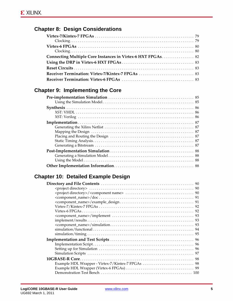
Chapter 8: Design ConsiderationsVirtex-7/Kintex-7 FPGAs . . . . . . . . . . . . . . . . . . . . . . . . . . . . . . . . . . . . . . . . . . . . . . . . . . . . 79
Clocking . . . . . . . . . . . . . . . . . . . . . . . . . . . . . . . . . . . . . . . . . . . . . . . . . . . . . . . . . . . . . . . . . 79Virtex-6 FPGAs . . . . . . . . . . . . . . . . . . . . . . . . . . . . . . . . . . . . . . . . . . . . . . . . . . . . . . . . . . . . . 80
Clocking . . . . . . . . . . . . . . . . . . . . . . . . . . . . . . . . . . . . . . . . . . . . . . . . . . . . . . . . . . . . . . . . . 80Connecting Multiple Core Instances in Virtex-6 HXT FPGAs. . . . . . . . . . . . . . . . . 82Using the DRP in Virtex-6 HXT FPGAs . . . . . . . . . . . . . . . . . . . . . . . . . . . . . . . . . . . . . . 83Reset Circuits . . . . . . . . . . . . . . . . . . . . . . . . . . . . . . . . . . . . . . . . . . . . . . . . . . . . . . . . . . . . . . . 83Receiver Termination: Virtex-7/Kintex-7 FPGAs . . . . . . . . . . . . . . . . . . . . . . . . . . . . . 83Receiver Termination: Virtex-6 FPGAs . . . . . . . . . . . . . . . . . . . . . . . . . . . . . . . . . . . . . . 83
Chapter 9: Implementing the CorePre-implementation Simulation . . . . . . . . . . . . . . . . . . . . . . . . . . . . . . . . . . . . . . . . . . . . . 85
Using the Simulation Model . . . . . . . . . . . . . . . . . . . . . . . . . . . . . . . . . . . . . . . . . . . . . . . . 85Synthesis . . . . . . . . . . . . . . . . . . . . . . . . . . . . . . . . . . . . . . . . . . . . . . . . . . . . . . . . . . . . . . . . . . . 86
XST: VHDL . . . . . . . . . . . . . . . . . . . . . . . . . . . . . . . . . . . . . . . . . . . . . . . . . . . . . . . . . . . . . . 86XST: Verilog . . . . . . . . . . . . . . . . . . . . . . . . . . . . . . . . . . . . . . . . . . . . . . . . . . . . . . . . . . . . . 86
Implementation . . . . . . . . . . . . . . . . . . . . . . . . . . . . . . . . . . . . . . . . . . . . . . . . . . . . . . . . . . . . . 87Generating the Xilinx Netlist . . . . . . . . . . . . . . . . . . . . . . . . . . . . . . . . . . . . . . . . . . . . . . . 87Mapping the Design . . . . . . . . . . . . . . . . . . . . . . . . . . . . . . . . . . . . . . . . . . . . . . . . . . . . . . 87Placing and Routing the Design . . . . . . . . . . . . . . . . . . . . . . . . . . . . . . . . . . . . . . . . . . . . 87Static Timing Analysis . . . . . . . . . . . . . . . . . . . . . . . . . . . . . . . . . . . . . . . . . . . . . . . . . . . . . 87Generating a Bitstream . . . . . . . . . . . . . . . . . . . . . . . . . . . . . . . . . . . . . . . . . . . . . . . . . . . . 87
Post-Implementation Simulation . . . . . . . . . . . . . . . . . . . . . . . . . . . . . . . . . . . . . . . . . . . . 88Generating a Simulation Model . . . . . . . . . . . . . . . . . . . . . . . . . . . . . . . . . . . . . . . . . . . . . 88Using the Model . . . . . . . . . . . . . . . . . . . . . . . . . . . . . . . . . . . . . . . . . . . . . . . . . . . . . . . . . . 88
Other Implementation Information . . . . . . . . . . . . . . . . . . . . . . . . . . . . . . . . . . . . . . . . . . 88
Chapter 10: Detailed Example DesignDirectory and File Contents . . . . . . . . . . . . . . . . . . . . . . . . . . . . . . . . . . . . . . . . . . . . . . . . . 90
<project directory> . . . . . . . . . . . . . . . . . . . . . . . . . . . . . . . . . . . . . . . . . . . . . . . . . . . . . . . 90<project directory>/<component name> . . . . . . . . . . . . . . . . . . . . . . . . . . . . . . . . . . . . 90<component_name>/doc . . . . . . . . . . . . . . . . . . . . . . . . . . . . . . . . . . . . . . . . . . . . . . . . . . 91<component_name>/example_design . . . . . . . . . . . . . . . . . . . . . . . . . . . . . . . . . . . . . . . 91Virtex-7/Kintex-7 FPGAs . . . . . . . . . . . . . . . . . . . . . . . . . . . . . . . . . . . . . . . . . . . . . . . . . . 92Virtex-6 FPGAs . . . . . . . . . . . . . . . . . . . . . . . . . . . . . . . . . . . . . . . . . . . . . . . . . . . . . . . . . . . 92<component_name>/implement . . . . . . . . . . . . . . . . . . . . . . . . . . . . . . . . . . . . . . . . . . . 93implement/results . . . . . . . . . . . . . . . . . . . . . . . . . . . . . . . . . . . . . . . . . . . . . . . . . . . . . . . . 93<component_name>/simulation . . . . . . . . . . . . . . . . . . . . . . . . . . . . . . . . . . . . . . . . . . . . 93simulation/functional . . . . . . . . . . . . . . . . . . . . . . . . . . . . . . . . . . . . . . . . . . . . . . . . . . . . . 94simulation/timing . . . . . . . . . . . . . . . . . . . . . . . . . . . . . . . . . . . . . . . . . . . . . . . . . . . . . . . . 95
Implementation and Test Scripts . . . . . . . . . . . . . . . . . . . . . . . . . . . . . . . . . . . . . . . . . . . . 96Implementation Script . . . . . . . . . . . . . . . . . . . . . . . . . . . . . . . . . . . . . . . . . . . . . . . . . . . . . 96Setting up for Simulation . . . . . . . . . . . . . . . . . . . . . . . . . . . . . . . . . . . . . . . . . . . . . . . . . . 96Simulation Scripts . . . . . . . . . . . . . . . . . . . . . . . . . . . . . . . . . . . . . . . . . . . . . . . . . . . . . . . . 97
10GBASE-R Core. . . . . . . . . . . . . . . . . . . . . . . . . . . . . . . . . . . . . . . . . . . . . . . . . . . . . . . . . . . . 98Example HDL Wrapper - Virtex-7/Kintex-7 FPGAs . . . . . . . . . . . . . . . . . . . . . . . . . . . 98Example HDL Wrapper (Virtex-6 FPGAs) . . . . . . . . . . . . . . . . . . . . . . . . . . . . . . . . . . . . 99Demonstration Test Bench . . . . . . . . . . . . . . . . . . . . . . . . . . . . . . . . . . . . . . . . . . . . . . . . 100
LogiCORE 10GBASE-R User Guide www.xilinx.com 5UG692 March 1, 2011
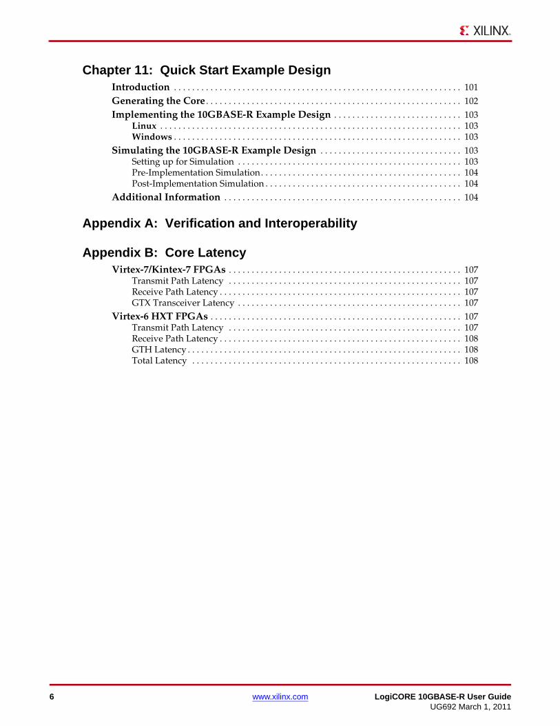
Chapter 11: Quick Start Example DesignIntroduction . . . . . . . . . . . . . . . . . . . . . . . . . . . . . . . . . . . . . . . . . . . . . . . . . . . . . . . . . . . . . . . 101Generating the Core . . . . . . . . . . . . . . . . . . . . . . . . . . . . . . . . . . . . . . . . . . . . . . . . . . . . . . . . 102Implementing the 10GBASE-R Example Design . . . . . . . . . . . . . . . . . . . . . . . . . . . . 103
Linux . . . . . . . . . . . . . . . . . . . . . . . . . . . . . . . . . . . . . . . . . . . . . . . . . . . . . . . . . . . . . . . . . . 103Windows . . . . . . . . . . . . . . . . . . . . . . . . . . . . . . . . . . . . . . . . . . . . . . . . . . . . . . . . . . . . . . . 103
Simulating the 10GBASE-R Example Design . . . . . . . . . . . . . . . . . . . . . . . . . . . . . . . 103Setting up for Simulation . . . . . . . . . . . . . . . . . . . . . . . . . . . . . . . . . . . . . . . . . . . . . . . . . 103Pre-Implementation Simulation . . . . . . . . . . . . . . . . . . . . . . . . . . . . . . . . . . . . . . . . . . . . 104Post-Implementation Simulation . . . . . . . . . . . . . . . . . . . . . . . . . . . . . . . . . . . . . . . . . . . 104
Additional Information . . . . . . . . . . . . . . . . . . . . . . . . . . . . . . . . . . . . . . . . . . . . . . . . . . . . 104
Appendix A: Verification and Interoperability
Appendix B: Core LatencyVirtex-7/Kintex-7 FPGAs . . . . . . . . . . . . . . . . . . . . . . . . . . . . . . . . . . . . . . . . . . . . . . . . . . . 107
Transmit Path Latency . . . . . . . . . . . . . . . . . . . . . . . . . . . . . . . . . . . . . . . . . . . . . . . . . . . 107Receive Path Latency . . . . . . . . . . . . . . . . . . . . . . . . . . . . . . . . . . . . . . . . . . . . . . . . . . . . . 107GTX Transceiver Latency . . . . . . . . . . . . . . . . . . . . . . . . . . . . . . . . . . . . . . . . . . . . . . . . . 107
Virtex-6 HXT FPGAs . . . . . . . . . . . . . . . . . . . . . . . . . . . . . . . . . . . . . . . . . . . . . . . . . . . . . . . 107Transmit Path Latency . . . . . . . . . . . . . . . . . . . . . . . . . . . . . . . . . . . . . . . . . . . . . . . . . . . 107Receive Path Latency . . . . . . . . . . . . . . . . . . . . . . . . . . . . . . . . . . . . . . . . . . . . . . . . . . . . . 108GTH Latency . . . . . . . . . . . . . . . . . . . . . . . . . . . . . . . . . . . . . . . . . . . . . . . . . . . . . . . . . . . . 108Total Latency . . . . . . . . . . . . . . . . . . . . . . . . . . . . . . . . . . . . . . . . . . . . . . . . . . . . . . . . . . . 108
6 www.xilinx.com LogiCORE 10GBASE-R User GuideUG692 March 1, 2011
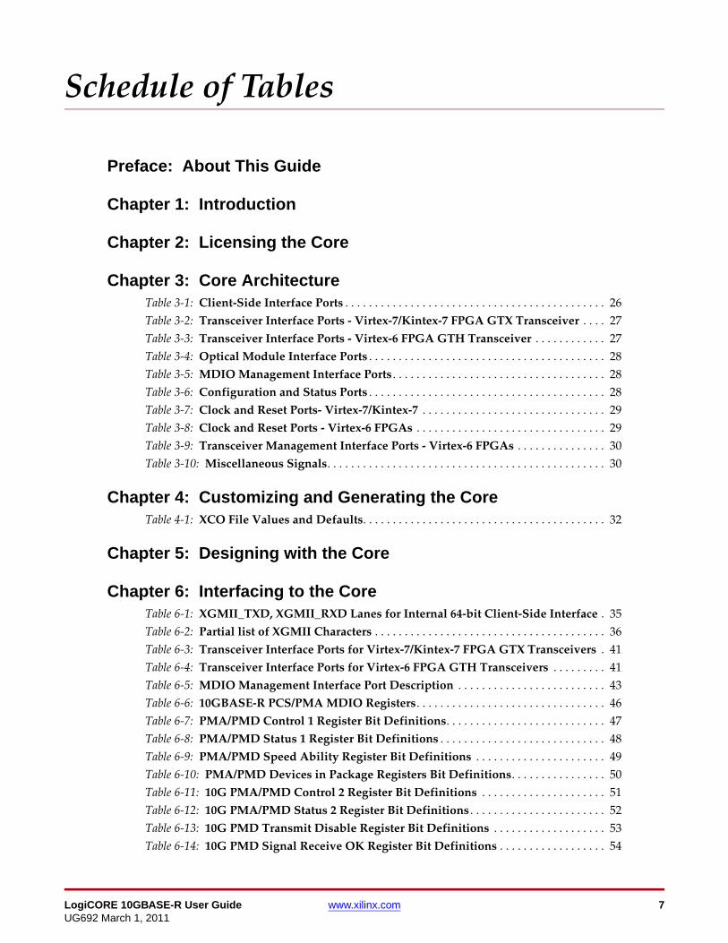
Schedule of Tables
Preface: About This Guide
Chapter 1: Introduction
Chapter 2: Licensing the Core
Chapter 3: Core ArchitectureTable 3-1: Client-Side Interface Ports . . . . . . . . . . . . . . . . . . . . . . . . . . . . . . . . . . . . . . . . . . . . 26Table 3-2: Transceiver Interface Ports - Virtex-7/Kintex-7 FPGA GTX Transceiver . . . . 27Table 3-3: Transceiver Interface Ports - Virtex-6 FPGA GTH Transceiver . . . . . . . . . . . . 27Table 3-4: Optical Module Interface Ports . . . . . . . . . . . . . . . . . . . . . . . . . . . . . . . . . . . . . . . . 28Table 3-5: MDIO Management Interface Ports . . . . . . . . . . . . . . . . . . . . . . . . . . . . . . . . . . . . 28Table 3-6: Configuration and Status Ports . . . . . . . . . . . . . . . . . . . . . . . . . . . . . . . . . . . . . . . . 28Table 3-7: Clock and Reset Ports- Virtex-7/Kintex-7 . . . . . . . . . . . . . . . . . . . . . . . . . . . . . . . 29Table 3-8: Clock and Reset Ports - Virtex-6 FPGAs . . . . . . . . . . . . . . . . . . . . . . . . . . . . . . . . 29Table 3-9: Transceiver Management Interface Ports - Virtex-6 FPGAs . . . . . . . . . . . . . . . 30Table 3-10: Miscellaneous Signals. . . . . . . . . . . . . . . . . . . . . . . . . . . . . . . . . . . . . . . . . . . . . . . 30
Chapter 4: Customizing and Generating the CoreTable 4-1: XCO File Values and Defaults. . . . . . . . . . . . . . . . . . . . . . . . . . . . . . . . . . . . . . . . . 32
Chapter 5: Designing with the Core
Chapter 6: Interfacing to the CoreTable 6-1: XGMII_TXD, XGMII_RXD Lanes for Internal 64-bit Client-Side Interface . 35Table 6-2: Partial list of XGMII Characters . . . . . . . . . . . . . . . . . . . . . . . . . . . . . . . . . . . . . . . 36Table 6-3: Transceiver Interface Ports for Virtex-7/Kintex-7 FPGA GTX Transceivers . 41Table 6-4: Transceiver Interface Ports for Virtex-6 FPGA GTH Transceivers . . . . . . . . . 41Table 6-5: MDIO Management Interface Port Description . . . . . . . . . . . . . . . . . . . . . . . . . 43Table 6-6: 10GBASE-R PCS/PMA MDIO Registers. . . . . . . . . . . . . . . . . . . . . . . . . . . . . . . . 46Table 6-7: PMA/PMD Control 1 Register Bit Definitions. . . . . . . . . . . . . . . . . . . . . . . . . . . 47Table 6-8: PMA/PMD Status 1 Register Bit Definitions . . . . . . . . . . . . . . . . . . . . . . . . . . . . 48Table 6-9: PMA/PMD Speed Ability Register Bit Definitions . . . . . . . . . . . . . . . . . . . . . . 49Table 6-10: PMA/PMD Devices in Package Registers Bit Definitions. . . . . . . . . . . . . . . . 50Table 6-11: 10G PMA/PMD Control 2 Register Bit Definitions . . . . . . . . . . . . . . . . . . . . . 51Table 6-12: 10G PMA/PMD Status 2 Register Bit Definitions . . . . . . . . . . . . . . . . . . . . . . . 52Table 6-13: 10G PMD Transmit Disable Register Bit Definitions . . . . . . . . . . . . . . . . . . . 53Table 6-14: 10G PMD Signal Receive OK Register Bit Definitions . . . . . . . . . . . . . . . . . . 54
LogiCORE 10GBASE-R User Guide www.xilinx.com 7UG692 March 1, 2011
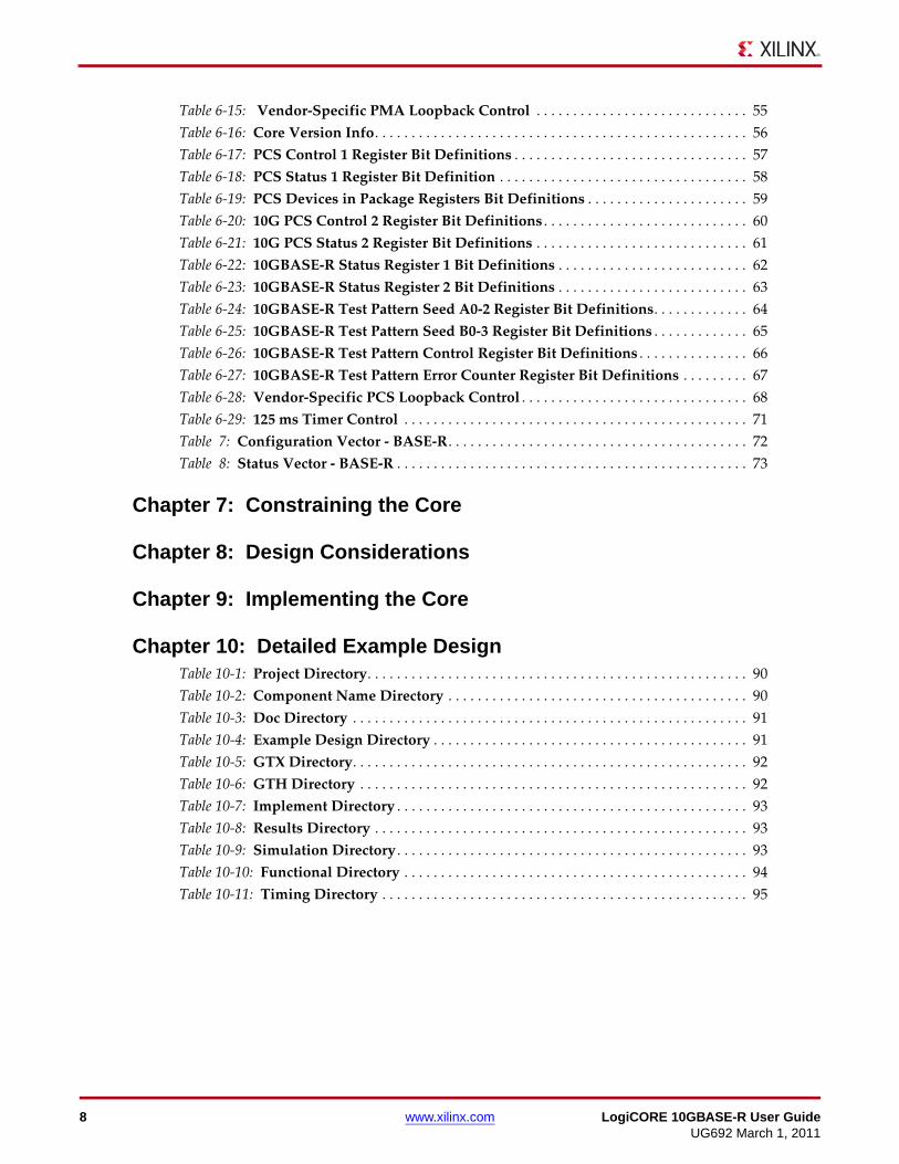
Table 6-15: Vendor-Specific PMA Loopback Control . . . . . . . . . . . . . . . . . . . . . . . . . . . . . 55Table 6-16: Core Version Info. . . . . . . . . . . . . . . . . . . . . . . . . . . . . . . . . . . . . . . . . . . . . . . . . . . 56Table 6-17: PCS Control 1 Register Bit Definitions . . . . . . . . . . . . . . . . . . . . . . . . . . . . . . . . 57Table 6-18: PCS Status 1 Register Bit Definition . . . . . . . . . . . . . . . . . . . . . . . . . . . . . . . . . . 58Table 6-19: PCS Devices in Package Registers Bit Definitions . . . . . . . . . . . . . . . . . . . . . . 59Table 6-20: 10G PCS Control 2 Register Bit Definitions . . . . . . . . . . . . . . . . . . . . . . . . . . . . 60Table 6-21: 10G PCS Status 2 Register Bit Definitions . . . . . . . . . . . . . . . . . . . . . . . . . . . . . 61Table 6-22: 10GBASE-R Status Register 1 Bit Definitions . . . . . . . . . . . . . . . . . . . . . . . . . . 62Table 6-23: 10GBASE-R Status Register 2 Bit Definitions . . . . . . . . . . . . . . . . . . . . . . . . . . 63Table 6-24: 10GBASE-R Test Pattern Seed A0-2 Register Bit Definitions. . . . . . . . . . . . . 64Table 6-25: 10GBASE-R Test Pattern Seed B0-3 Register Bit Definitions . . . . . . . . . . . . . 65Table 6-26: 10GBASE-R Test Pattern Control Register Bit Definitions . . . . . . . . . . . . . . . 66Table 6-27: 10GBASE-R Test Pattern Error Counter Register Bit Definitions . . . . . . . . . 67Table 6-28: Vendor-Specific PCS Loopback Control . . . . . . . . . . . . . . . . . . . . . . . . . . . . . . . 68Table 6-29: 125 ms Timer Control . . . . . . . . . . . . . . . . . . . . . . . . . . . . . . . . . . . . . . . . . . . . . . . 71Table 7: Configuration Vector - BASE-R. . . . . . . . . . . . . . . . . . . . . . . . . . . . . . . . . . . . . . . . . 72Table 8: Status Vector - BASE-R . . . . . . . . . . . . . . . . . . . . . . . . . . . . . . . . . . . . . . . . . . . . . . . . 73
Chapter 7: Constraining the Core
Chapter 8: Design Considerations
Chapter 9: Implementing the Core
Chapter 10: Detailed Example DesignTable 10-1: Project Directory. . . . . . . . . . . . . . . . . . . . . . . . . . . . . . . . . . . . . . . . . . . . . . . . . . . . 90Table 10-2: Component Name Directory . . . . . . . . . . . . . . . . . . . . . . . . . . . . . . . . . . . . . . . . . 90Table 10-3: Doc Directory . . . . . . . . . . . . . . . . . . . . . . . . . . . . . . . . . . . . . . . . . . . . . . . . . . . . . . 91Table 10-4: Example Design Directory . . . . . . . . . . . . . . . . . . . . . . . . . . . . . . . . . . . . . . . . . . . 91Table 10-5: GTX Directory. . . . . . . . . . . . . . . . . . . . . . . . . . . . . . . . . . . . . . . . . . . . . . . . . . . . . . 92Table 10-6: GTH Directory . . . . . . . . . . . . . . . . . . . . . . . . . . . . . . . . . . . . . . . . . . . . . . . . . . . . . 92Table 10-7: Implement Directory . . . . . . . . . . . . . . . . . . . . . . . . . . . . . . . . . . . . . . . . . . . . . . . . 93Table 10-8: Results Directory . . . . . . . . . . . . . . . . . . . . . . . . . . . . . . . . . . . . . . . . . . . . . . . . . . . 93Table 10-9: Simulation Directory . . . . . . . . . . . . . . . . . . . . . . . . . . . . . . . . . . . . . . . . . . . . . . . . 93Table 10-10: Functional Directory . . . . . . . . . . . . . . . . . . . . . . . . . . . . . . . . . . . . . . . . . . . . . . . 94Table 10-11: Timing Directory . . . . . . . . . . . . . . . . . . . . . . . . . . . . . . . . . . . . . . . . . . . . . . . . . . 95
8 www.xilinx.com LogiCORE 10GBASE-R User GuideUG692 March 1, 2011
Chapter 11: Quick Start Example Design
Appendix A: Verification and Interoperability
Appendix B: Core Latency
LogiCORE 10GBASE-R User Guide www.xilinx.com 9UG692 March 1, 2011
Schedule of Figures
Preface: About This Guide
Chapter 1: Introduction
Chapter 2: Licensing the Core
Chapter 3: Core ArchitectureFigure 3-1: Virtex-7/Kintex-7 Implementation of the 10-Gigabit Ethernet
PCS/PMA (BASE-R) Core. . . . . . . . . . . . . . . . . . . . . . . . . . . . . . . . . . . . . . . . . . . . . . . . . . . . 24Figure 3-2: Virtex-6 Implementation of the 10-Gigabit Ethernet
PCS/PMA (BASE-R) Core. . . . . . . . . . . . . . . . . . . . . . . . . . . . . . . . . . . . . . . . . . . . . . . . . . . . 25Figure 3-3: Typical Ethernet System Architecture . . . . . . . . . . . . . . . . . . . . . . . . . . . . . . . . . 25Figure 3-4: 10-Gigabit Ethernet PCS/PMA Core Connected to MAC
Core Using XGMII Interface . . . . . . . . . . . . . . . . . . . . . . . . . . . . . . . . . . . . . . . . . . . . . . . . . 26
Chapter 4: Customizing and Generating the CoreFigure 4-1: 10GBASE-R Main Screen . . . . . . . . . . . . . . . . . . . . . . . . . . . . . . . . . . . . . . . . . . . . 31
Chapter 5: Designing with the Core
Chapter 6: Interfacing to the CoreFigure 6-1: Normal Frame Transmission Across the Internal 64-bit Client-Side I/F. . . . 37Figure 6-2: Frame Transmission with Error Across Internal 64-bit Client-Side I/F. . . . . 38Figure 6-3: Frame Reception Across the Internal 64-bit Client Interface . . . . . . . . . . . . . 39Figure 6-4: Frame Reception with Error Across the Internal 64-bit Client Interface . . . 40Figure 6-5: A Typical MDIO-Managed System . . . . . . . . . . . . . . . . . . . . . . . . . . . . . . . . . . . 42Figure 6-6: MDIO Set Address Transaction . . . . . . . . . . . . . . . . . . . . . . . . . . . . . . . . . . . . . . 44Figure 6-7: MDIO Write Transaction . . . . . . . . . . . . . . . . . . . . . . . . . . . . . . . . . . . . . . . . . . . . 44Figure 6-8: MDIO Read Transaction. . . . . . . . . . . . . . . . . . . . . . . . . . . . . . . . . . . . . . . . . . . . . 44Figure 6-9: MDIO Read-and-increment Transaction. . . . . . . . . . . . . . . . . . . . . . . . . . . . . . . 45Figure 6-10: PMA/PMD Control 1 Register . . . . . . . . . . . . . . . . . . . . . . . . . . . . . . . . . . . . . . . 47Figure 6-11: PMA/PMD Status 1 Register . . . . . . . . . . . . . . . . . . . . . . . . . . . . . . . . . . . . . . . . 48Figure 6-12: PMA/PMD Speed Ability Register. . . . . . . . . . . . . . . . . . . . . . . . . . . . . . . . . . . 49Figure 6-13: PMA/PMD Devices in Package Registers . . . . . . . . . . . . . . . . . . . . . . . . . . . . . 49Figure 6-14: 10G PMA/PMD Control 2 Register. . . . . . . . . . . . . . . . . . . . . . . . . . . . . . . . . . . 51Figure 6-15: 10G PMA/PMD Status 2 Register . . . . . . . . . . . . . . . . . . . . . . . . . . . . . . . . . . . . 52Figure 6-16: 10G PMD Transmit Disable Register. . . . . . . . . . . . . . . . . . . . . . . . . . . . . . . . . 53Figure 6-17: 10G PMD Signal Receive OK Register . . . . . . . . . . . . . . . . . . . . . . . . . . . . . . . 54
LogiCORE 10GBASE-R User Guide www.xilinx.com 11UG692 March 1, 2011
Figure 6-18: Vendor-Specific PMA Loopback Control Register . . . . . . . . . . . . . . . . . . . . . 54Figure 6-19: Core Version Info Register. . . . . . . . . . . . . . . . . . . . . . . . . . . . . . . . . . . . . . . . . . 56Figure 6-20: PCS Control 1 Register . . . . . . . . . . . . . . . . . . . . . . . . . . . . . . . . . . . . . . . . . . . . . 57Figure 6-21: PCS Status 1 Register . . . . . . . . . . . . . . . . . . . . . . . . . . . . . . . . . . . . . . . . . . . . . . 58Figure 6-22: PCS Devices in Package Registers . . . . . . . . . . . . . . . . . . . . . . . . . . . . . . . . . . . 59Figure 6-23: 10G PCS Control 2 Register . . . . . . . . . . . . . . . . . . . . . . . . . . . . . . . . . . . . . . . . . 60Figure 6-24: 10G PCS Status 2 Register . . . . . . . . . . . . . . . . . . . . . . . . . . . . . . . . . . . . . . . . . . 61Figure 6-25: 10GBASE-R Status Register 1 . . . . . . . . . . . . . . . . . . . . . . . . . . . . . . . . . . . . . . . 62Figure 6-26: 10GBASE-R Status Register 2 . . . . . . . . . . . . . . . . . . . . . . . . . . . . . . . . . . . . . . . 63Figure 6-27: 10GBASE-R Test Pattern Seed A0-3 Registers . . . . . . . . . . . . . . . . . . . . . . . . . 64Figure 6-28: 10GBASE-R Test Pattern Seed B0-3 Registers . . . . . . . . . . . . . . . . . . . . . . . . . 65Figure 6-29: 10GBASE-R Test Pattern Control Register . . . . . . . . . . . . . . . . . . . . . . . . . . . . 66Figure 6-30: 10GBASE-R Test Pattern Error Counter Register . . . . . . . . . . . . . . . . . . . . . . 67Figure 6-31: Vendor-Specific PCS Loopback Control Register . . . . . . . . . . . . . . . . . . . . . . 68Figure 6-32: 25 μs Timer Control Register . . . . . . . . . . . . . . . . . . . . . . . . . . . . . . . . . . . . . . . . 71Figure 6-33: Clearing the Latching-High Bits . . . . . . . . . . . . . . . . . . . . . . . . . . . . . . . . . . . . . 73Figure 6-34: Setting the Latching-Low Bits . . . . . . . . . . . . . . . . . . . . . . . . . . . . . . . . . . . . . . . 74
Chapter 7: Constraining the Core
Chapter 8: Design ConsiderationsFigure 8-1: Clocking Scheme for Internal Client-Side Interface:
Virtex-7/Kintex-7 FPGAs . . . . . . . . . . . . . . . . . . . . . . . . . . . . . . . . . . . . . . . . . . . . . . . . . . . . 80Figure 8-2: Clock Scheme for Internal Client-Side Interface:
Virtex-6 HXT FPGAs . . . . . . . . . . . . . . . . . . . . . . . . . . . . . . . . . . . . . . . . . . . . . . . . . . . . . . . . 81Figure 8-3: Attaching Multiple Cores to a GTH_QUAD Tile . . . . . . . . . . . . . . . . . . . . . . . 82
Chapter 9: Implementing the Core
Chapter 10: Detailed Example DesignFigure 10-1: Example HDL Wrapper for 10GBASE-R (Virtex-7/Kintex-7 FPGAs) . . . . . 98Figure 10-2: Example HDL Wrapper for 10GBASE-R (Virtex-6 FPGAs) . . . . . . . . . . . . . . 99Figure 10-3: Demonstration Test Bench for 10GBASE-R . . . . . . . . . . . . . . . . . . . . . . . . . . 100
Chapter 11: Quick Start Example DesignFigure 11-1: Virtex-7/Kintex-7 FPGA 10GBASE-R Example Design and Test Bench . . 101Figure 11-2: Virtex-6 FPGA 10GBASE-R Example Design
and Test Bench with MDIO. . . . . . . . . . . . . . . . . . . . . . . . . . . . . . . . . . . . . . . . . . . . . . . . . 102
Appendix A: Verification and Interoperability
Appendix B: Core Latency
12 www.xilinx.com LogiCORE 10GBASE-R User GuideUG692 March 1, 2011
Preface
About This Guide
The Ten Gigabit Ethernet PCS/PMA v2.1 User Guide provides information about generating a LogiCORE™ IP Ten Gigabit Ethernet PCS/PMA (10GBASE-R) core, customizing and simulating the core utilizing the provided example design, and running the design files through implementation using the Xilinx tools.
Guide ContentsThis guide contains these chapters and appendixes:
• About This Guide introduces you to the organization and purpose of the design guide and describes the conventions used in this document.
• Chapter 1, Introduction, introduces the 10GBASE-R core and provides related information, including recommended design experience, additional resources, technical support, and submitting feedback to Xilinx.
• Chapter 2, Licensing the Core, describes how to get a license for the core.
• Chapter 3, Core Architecture, describes the overall architecture of the 10GBASE-R core and also describes the major interfaces to the core.
• Chapter 4, Customizing and Generating the Core, describes how to customize the 10GBASE-R core for specific applications and generate the core netlist using Xilinx® CORE Generator™ software.
• Chapter 5, Designing with the Core, contains a general description of how to use the 10GBASE-R core in your own design.
• Chapter 6, Interfacing to the Core, defines the data interfaces and the configuration and status interfaces available for dynamically setting configuration and status.
• Chapter 7, Constraining the Core, describes how to constrain a design, illustrated by the default user constraints file (UCF) included with the 10GBASE-R core.
• Chapter 8, Design Considerations, describes considerations that can apply in specific design cases.
• Chapter 9, Implementing the Core, describes how to simulate and implement your design containing the 10GBASE-R core.
• Chapter 10, Detailed Example Design, describes the Example Design delivered with the core.
• Chapter 11, Quick Start Example Design, describes how to get up and running with the Example Design.
• Appendix A, Verification and Interoperability, describes the 10GBASE-R verification methods in simulation and hardware testing environments.
• Appendix B, Core Latency, describe these measurements are for the core only - they do not include the latency through the transceiver.
LogiCORE 10GBASE-R User Guide www.xilinx.com 13UG692 March 1, 2011
Preface: About This Guide
Additional ResourcesTo find additional documentation, see the Xilinx website at:
www.xilinx.com/support/documentation/index.htm.
To search the Answer Database of silicon, software, and IP questions and answers, or to create a technical support WebCase, see the Xilinx website at:
www.xilinx.com/support.
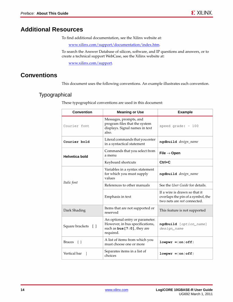
ConventionsThis document uses the following conventions. An example illustrates each convention.
TypographicalThese typographical conventions are used in this document:
Convention Meaning or Use Example
Courier font
Messages, prompts, and program files that the system displays. Signal names in text also.
speed grade: - 100
Courier boldLiteral commands that you enter in a syntactical statement
ngdbuild design_name
Helvetica bold
Commands that you select from a menu
File → Open
Keyboard shortcuts Ctrl+C
Italic font
Variables in a syntax statement for which you must supply values
ngdbuild design_name
References to other manuals See the User Guide for details.
Emphasis in textIf a wire is drawn so that it overlaps the pin of a symbol, the two nets are not connected.
Dark ShadingItems that are not supported or reserved
This feature is not supported
Square brackets [ ]
An optional entry or parameter. However, in bus specifications, such as bus[7:0], they are required.
ngdbuild [option_name] design_name
Braces { }A list of items from which you must choose one or more lowpwr ={on|off}
Vertical bar |Separates items in a list of choices lowpwr ={on|off}
14 www.xilinx.com LogiCORE 10GBASE-R User GuideUG692 March 1, 2011
Conventions
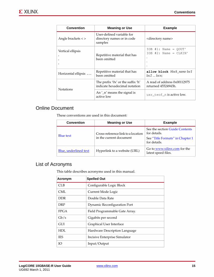
Online DocumentThese conventions are used in this document:
Convention Meaning or Use Example
See the section Guide Contents for details.
See “Title Formats” in Chapter 1 for details.
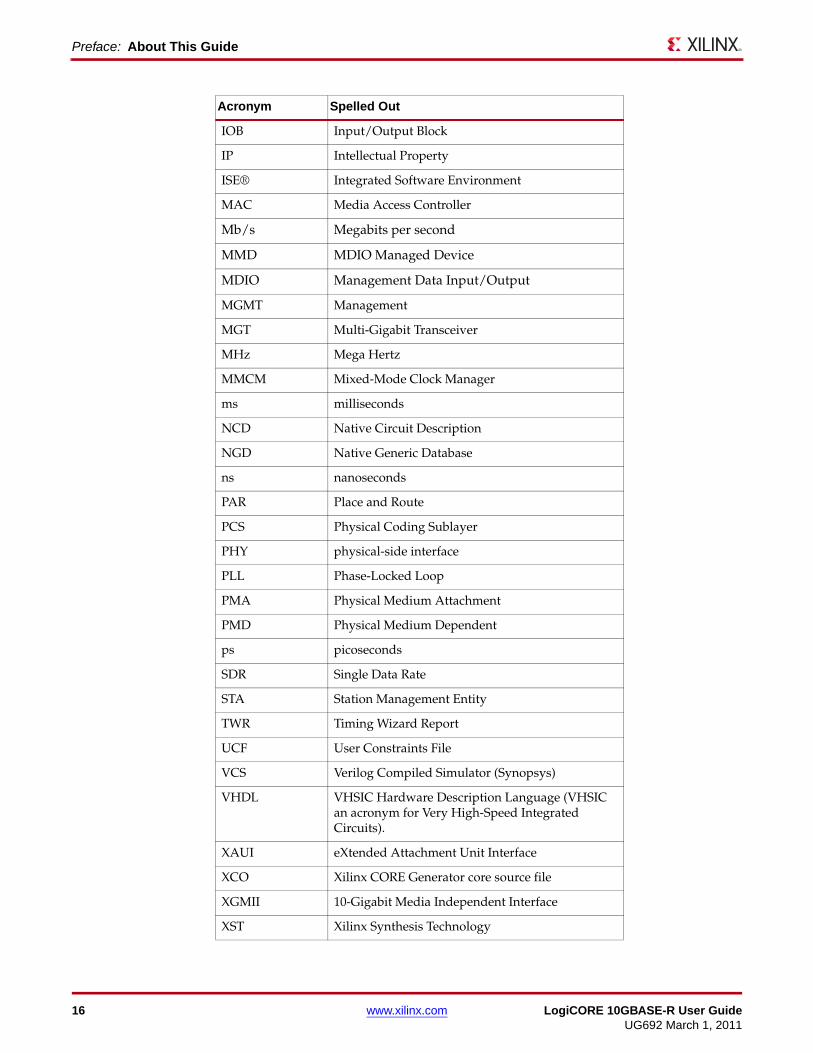
List of AcronymsThis table describes acronyms used in this manual.
Angle brackets < >User-defined variable for directory names or in code samples
<directory name>
Vertical ellipsis . . .
Repetitive material that has been omitted
IOB #1: Name = QOUT’ IOB #2: Name = CLKIN’ . . .
Horizontal ellipsis . . .Repetitive material that has been omitted
allow block block_name loc1 loc2 ... locn;
Notations
The prefix ‘0x’ or the suffix ‘h’ indicate hexadecimal notation
A read of address 0x00112975 returned 45524943h.
An ‘_n’ means the signal is active low usr_teof_n is active low.
Convention Meaning or Use Example
Blue textCross-reference link to a location in the current document
Blue, underlined text Hyperlink to a website (URL)Go to www.xilinx.com for the latest speed files.
Acronym Spelled Out
CLB Configurable Logic Block
CML Current Mode Logic
DDR Double Data Rate
DRP Dynamic Reconfiguration Port
FPGA Field Programmable Gate Array.
Gb/s Gigabits per second
GUI Graphical User Interface
HDL Hardware Description Language
IES Incisive Enterprise Simulator
IO Input/Output
LogiCORE 10GBASE-R User Guide www.xilinx.com 15UG692 March 1, 2011
Preface: About This Guide
IOB Input/Output Block
IP Intellectual Property
ISE® Integrated Software Environment
MAC Media Access Controller
Mb/s Megabits per second
MMD MDIO Managed Device
MDIO Management Data Input/Output
MGMT Management
MGT Multi-Gigabit Transceiver
MHz Mega Hertz
MMCM Mixed-Mode Clock Manager
ms milliseconds
NCD Native Circuit Description
NGD Native Generic Database
ns nanoseconds
PAR Place and Route
PCS Physical Coding Sublayer
PHY physical-side interface
PLL Phase-Locked Loop
PMA Physical Medium Attachment
PMD Physical Medium Dependent
ps picoseconds
SDR Single Data Rate
STA Station Management Entity
TWR Timing Wizard Report
UCF User Constraints File
VCS Verilog Compiled Simulator (Synopsys)
VHDL VHSIC Hardware Description Language (VHSIC an acronym for Very High-Speed Integrated Circuits).
XAUI eXtended Attachment Unit Interface
XCO Xilinx CORE Generator core source file
XGMII 10-Gigabit Media Independent Interface
XST Xilinx Synthesis Technology
Acronym Spelled Out
16 www.xilinx.com LogiCORE 10GBASE-R User GuideUG692 March 1, 2011
Chapter 1
Introduction
The 10GBASE-R LogiCORE™ IP core has been verified in IDS 13.1 software with the pre-production Virtex®-6 HXT FPGA and Virtex-7/Kintex™-7 FPGA speed files. Pre-production means that the speed files are still subject to change. The 10GBASE-R LogiCORE IP core and example design are provided in Verilog and VHDL.
This chapter introduces the 10GBASE-R core and provides related information, including recommended design experience, additional resources, technical support, and submitting feedback to Xilinx.
System RequirementsWindows
• Windows XP Professional 32-bit/64-bit
• Windows Vista Business 32-bit/64-bit
Linux
• Red Hat Enterprise Linux WS v4.0 32-bit/64-bit
• Red Hat Enterprise Desktop v5.0 32-bit/64-bit (with Workstation Option)
• SUSE Linux Enterprise (SLE) v10.1 32-bit/64-bit
Software
• ISE® software v13.1
About the CoreThe 10GBASE-R core is a Xilinx® CORE Generator™ software IP core, included in the latest ISE Update on the Xilinx IP Center. For detailed information about the core, see the 10GBASE-R product page. For information about licensing options, see Chapter 2, Licensing the Core.
Recommended Design ExperienceAlthough the 10GBASE-R core is a fully-verified solution, the challenge associated with implementing a complete design varies depending on the configuration and functionality of the application. For best results, previous experience building high performance, pipelined FPGA designs using Xilinx implementation software and UCF is recommended.
Contact your local Xilinx representative for a closer review and estimation for your specific requirements.
LogiCORE 10GBASE-R User Guide www.xilinx.com 17UG692 March 1, 2011
Chapter 1: Introduction
Additional Core ResourcesFor detailed information about 10GBASE-R technology and updates to the 10GBASE-R core, see the following:
DocumentationFrom the 10GBASE-R product page:
• 10GBASE-R Release Notes
• 10GBASE-R Data Sheet
From the document directory after generating the core:
• 10GBASE-R Release Notes
• 10GBASE-R Data Sheet
10GBASE-R TechnologyFor information about 10GBASE-R technology basics, including features, FAQs, the 10GBASE-R chip interface, typical applications, specifications, and other important information, see www.xilinx.com/products/ipcenter/10GBASE-R.htm.
Ethernet SpecificationsThe relevant 10GBASE-R standards are IEEE Std. 802.3-2008.
Other InformationThe 10-Gigabit Ethernet Consortium at the University of New Hampshire Interoperability Lab is an excellent source of information on 10-Gigabit Ethernet technology: www.iol.unh.edu/consortiums/10gec/index.html.
Technical SupportFor technical support, visit www.xilinx.com/support. Questions are routed to a team of engineers with expertise using the 10GBASE-R core.
Xilinx provides technical support for use of this product as described in the LogiCORE IP 10GBASE-R User Guide. Xilinx cannot guarantee timing, functionality, or support of this product for designs that do not follow these guidelines.
18 www.xilinx.com LogiCORE 10GBASE-R User GuideUG692 March 1, 2011
Feedback
FeedbackXilinx welcomes comments and suggestions about the 10GBASE-R core and the documentation supplied with the core.
CoreFor comments or suggestions about the 10GBASE-R core, submit a webcase from www.xilinx.com/support. Be sure to include the following information:
• Product name
• Core version number
• Explanation of your comments
DocumentFor comments or suggestions about this document, submit a webcase from www.xilinx.com/support. Be sure to include the following information:
• Document title
• Document number
• Page number(s) to which your comments refer
• Explanation of your comments
LogiCORE 10GBASE-R User Guide www.xilinx.com 19UG692 March 1, 2011
Chapter 1: Introduction
20 www.xilinx.com LogiCORE 10GBASE-R User GuideUG692 March 1, 2011
Chapter 2
Licensing the Core
This core is provided under the End User License Agreement and can be generated using the Xilinx® CORE Generator™ system v13.1 or higher. The CORE Generator system is shipped with Xilinx ISE® Design Suite Series Development software. In ISE v13.1 software and later, a license key is not required to access the 10GBASE-R IP. To access the wrapper in ISE v12.4 software and older, a no-cost full license must be obtained from Xilinx. See the version of the user guide for the version of the core you are using for information.
Contact your local Xilinx sales representative for pricing and availability of other Xilinx LogiCORE IP modules and software. Information on additional LogiCORE IP modules is available at the Xilinx IP Center.
LogiCORE 10GBASE-R User Guide www.xilinx.com 21UG692 March 1, 2011

Chapter 2: Licensing the Core
22 www.xilinx.com LogiCORE 10GBASE-R User GuideUG692 March 1, 2011
Chapter 3
Core Architecture
This chapter describes the overall architecture of the 10GBASE-R core and also describes the major interfaces to the core.
System Overview10GBASE-R is a 10 Gb/s serial interface. It is intended to provide the PCS and PMA functionality between the XGMII interface on a Ten Gigabit Ethernet MAC and a Ten Gigabit Ethernet network PHY.
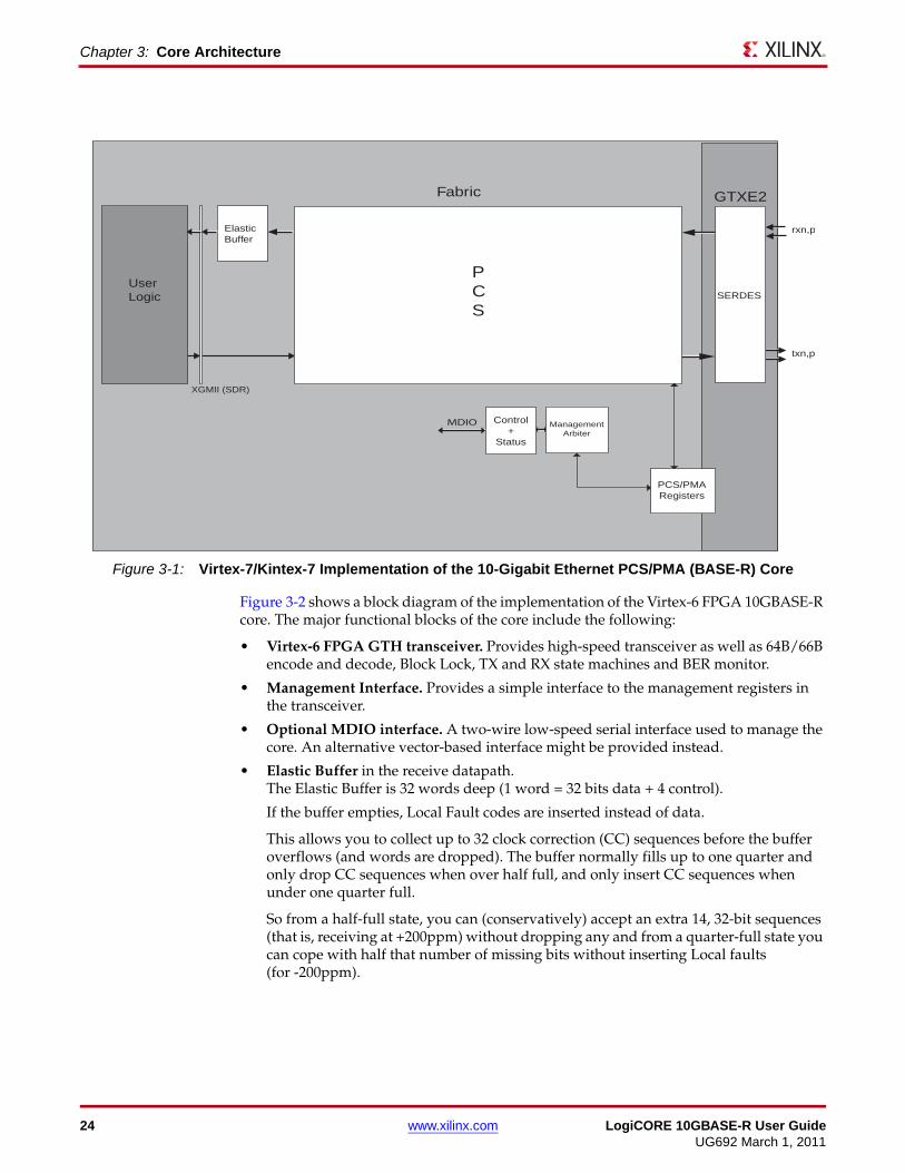
Functional DescriptionFigure 3-1 shows a block diagram of the implementation of the Virtex®-7/Kintex™-7 FPGA 10GBASE-R core. The major functional blocks of the core include the following:
• Virtex-7/Kintex-7 FPGA GTX Transceiver. Provides high-speed transceiver and partial gearbox functionality.
• PCS Block. Provides encode/decode, scramble/descramble, block-lock, transmit and receive state machines, test-pattern blocks and BER monitor, in the same configuration as in Figure 3-2.
• Optional MDIO Interface. A two-wire low-speed serial interface used to manage the core. An alternative vector-based interface might be provided instead.
• Elastic Buffer. Identical to that described in the next section. See page 24.
LogiCORE 10GBASE-R User Guide www.xilinx.com 23UG692 March 1, 2011
Chapter 3: Core Architecture
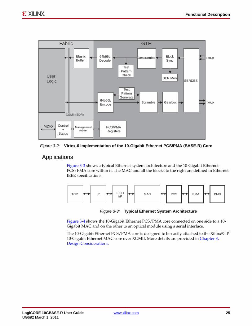
Figure 3-2 shows a block diagram of the implementation of the Virtex-6 FPGA 10GBASE-R core. The major functional blocks of the core include the following:
• Virtex-6 FPGA GTH transceiver. Provides high-speed transceiver as well as 64B/66B encode and decode, Block Lock, TX and RX state machines and BER monitor.
• Management Interface. Provides a simple interface to the management registers in the transceiver.
• Optional MDIO interface. A two-wire low-speed serial interface used to manage the core. An alternative vector-based interface might be provided instead.
• Elastic Buffer in the receive datapath. The Elastic Buffer is 32 words deep (1 word = 32 bits data + 4 control).
If the buffer empties, Local Fault codes are inserted instead of data.
This allows you to collect up to 32 clock correction (CC) sequences before the buffer overflows (and words are dropped). The buffer normally fills up to one quarter and only drop CC sequences when over half full, and only insert CC sequences when under one quarter full.
So from a half-full state, you can (conservatively) accept an extra 14, 32-bit sequences (that is, receiving at +200ppm) without dropping any and from a quarter-full state you can cope with half that number of missing bits without inserting Local faults (for -200ppm).
X-Ref Target - Figure 3-1
Figure 3-1: Virtex-7/Kintex-7 Implementation of the 10-Gigabit Ethernet PCS/PMA (BASE-R) Core
User Logic
XGMII (SDR)
Fabric
ElasticBuffer
Control+
Status
MDIO ManagementArbiter
PCS
SERDES
PCS/PMARegisters
GTXE2
rxn,p
txn,p
24 www.xilinx.com LogiCORE 10GBASE-R User GuideUG692 March 1, 2011
Functional Description
ApplicationsFigure 3-3 shows a typical Ethernet system architecture and the 10-Gigabit Ethernet PCS/PMA core within it. The MAC and all the blocks to the right are defined in Ethernet IEEE specifications.
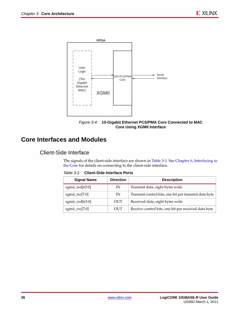
Figure 3-4 shows the 10-Gigabit Ethernet PCS/PMA core connected on one side to a 10-Gigabit MAC and on the other to an optical module using a serial interface.
The 10-Gigabit Ethernet PCS/PMA core is designed to be easily attached to the Xilinx® IP 10-Gigabit Ethernet MAC core over XGMII. More details are provided in Chapter 8, Design Considerations.
X-Ref Target - Figure 3-2
Figure 3-2: Virtex-6 Implementation of the 10-Gigabit Ethernet PCS/PMA (BASE-R) Core
User Logic
64b66bDecode
Descramble BlockSync
XGMII (SDR)
Fabric
ElasticBuffer
BER Mon
TestPatternCheck
64b66bEncode
TestPattern
Generate
Scramble Gearbox
GTH
SERDES
rxn,p
txn,p
Control+
Status
PCS/PMARegisters
MDIO ManagementArbiter
X-Ref Target - Figure 3-3
Figure 3-3: Typical Ethernet System Architecture
TCP IP FIFOI/F
MAC PCS PMA PMD
LogiCORE 10GBASE-R User Guide www.xilinx.com 25UG692 March 1, 2011
Chapter 3: Core Architecture
Core Interfaces and Modules
Client-Side InterfaceThe signals of the client-side interface are shown in Table 3-1. See Chapter 6, Interfacing to the Core for details on connecting to the client-side interface.
Signal Name Direction Description
xgmii_txd[63:0] Transmit data, eight bytes wide
xgmii_txc[7:0] Transmit control bits, one bit per transmit data byte
xgmii_rxd[63:0] Received data, eight bytes wide
xgmii_rxc[7:0] Receive control bits, one bit per received data byte
X-Ref Target - Figure 3-4
Figure 3-4: 10-Gigabit Ethernet PCS/PMA Core Connected to MAC Core Using XGMII Interface
UserLogic
(TenGigabit
EthernetMAC)
FPGA
10G PCS/PMACore
XGMII
Serial Interface
Table 3-1: Client-Side Interface Ports
IN
IN
OUT
OUT
26 www.xilinx.com LogiCORE 10GBASE-R User GuideUG692 March 1, 2011
Core Interfaces and Modules
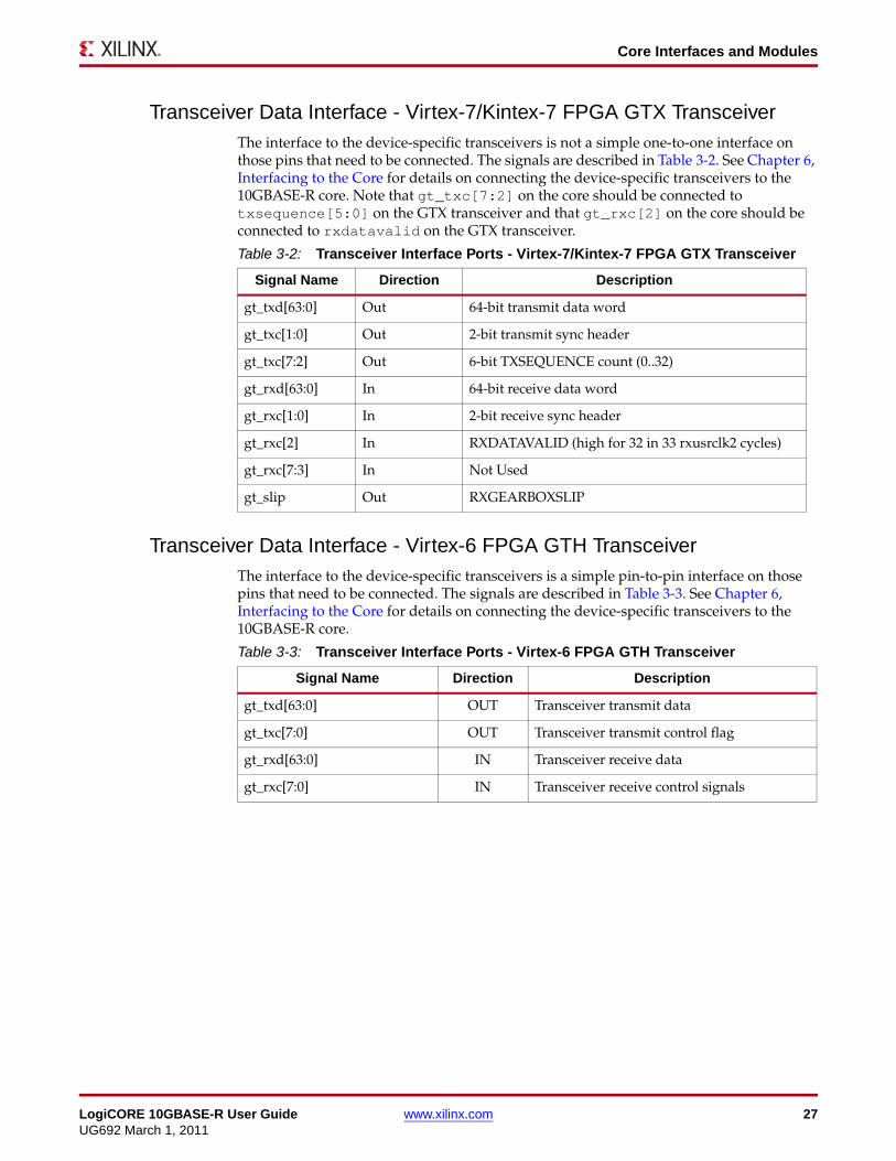
Transceiver Data Interface - Virtex-7/Kintex-7 FPGA GTX TransceiverThe interface to the device-specific transceivers is not a simple one-to-one interface on those pins that need to be connected. The signals are described in Table 3-2. See Chapter 6, Interfacing to the Core for details on connecting the device-specific transceivers to the 10GBASE-R core. Note that gt_txc[7:2] on the core should be connected to txsequence[5:0] on the GTX transceiver and that gt_rxc[2] on the core should be connected to rxdatavalid on the GTX transceiver.
Signal Name Direction Description
gt_txd[63:0] Out 64-bit transmit data word
gt_txc[1:0] Out 2-bit transmit sync header
gt_txc[7:2] Out 6-bit TXSEQUENCE count (0..32)
gt_rxd[63:0] In 64-bit receive data word
gt_rxc[1:0] In 2-bit receive sync header
gt_rxc[2] In RXDATAVALID (high for 32 in 33 rxusrclk2 cycles)
gt_rxc[7:3] In Not Used
gt_slip Out RXGEARBOXSLIP
Transceiver Data Interface - Virtex-6 FPGA GTH TransceiverThe interface to the device-specific transceivers is a simple pin-to-pin interface on those pins that need to be connected. The signals are described in Table 3-3. See Chapter 6, Interfacing to the Core for details on connecting the device-specific transceivers to the 10GBASE-R core.
Signal Name Direction Description
gt_txd[63:0] Transceiver transmit data
gt_txc[7:0] Transceiver transmit control flag
gt_rxd[63:0] Transceiver receive data
gt_rxc[7:0] Transceiver receive control signals
Table 3-2: Transceiver Interface Ports - Virtex-7/Kintex-7 FPGA GTX Transceiver
Table 3-3: Transceiver Interface Ports - Virtex-6 FPGA GTH Transceiver
OUT
OUT
IN
IN
LogiCORE 10GBASE-R User Guide www.xilinx.com 27UG692 March 1, 2011
Chapter 3: Core Architecture
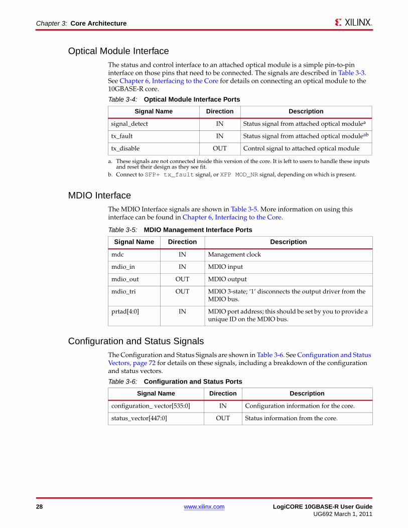
Optical Module InterfaceThe status and control interface to an attached optical module is a simple pin-to-pin interface on those pins that need to be connected. The signals are described in Table 3-3. See Chapter 6, Interfacing to the Core for details on connecting an optical module to the 10GBASE-R core.
Signal Name Direction Description
signal_detect Status signal from attached optical modulea
tx_fault Status signal from attached optical moduleab
tx_disable Control signal to attached optical module
MDIO InterfaceThe MDIO Interface signals are shown in Table 3-5. More information on using this interface can be found in Chapter 6, Interfacing to the Core.
Signal Name Direction Description
mdc Management clock
mdio_in MDIO input
mdio_out MDIO output
mdio_tri MDIO 3-state; ‘1’ disconnects the output driver from the MDIO bus.
prtad[4:0] MDIO port address; this should be set by you to provide a unique ID on the MDIO bus.
Configuration and Status SignalsThe Configuration and Status Signals are shown in Table 3-6. See Configuration and Status Vectors, page 72 for details on these signals, including a breakdown of the configuration and status vectors.
Signal Name Direction Description
configuration_ vector[535:0] Configuration information for the core.
status_vector[447:0] Status information from the core.
Table 3-4: Optical Module Interface Ports
IN
a. These signals are not connected inside this version of the core. It is left to users to handle these inputs and reset their design as they see fit.
IN
b. Connect to SFP+ tx_fault signal, or XFP MOD_NR signal, depending on which is present.
OUT
Table 3-5: MDIO Management Interface Ports
IN
IN
OUT
OUT
IN
Table 3-6: Configuration and Status Ports
IN
OUT
28 www.xilinx.com LogiCORE 10GBASE-R User GuideUG692 March 1, 2011
Core Interfaces and Modules
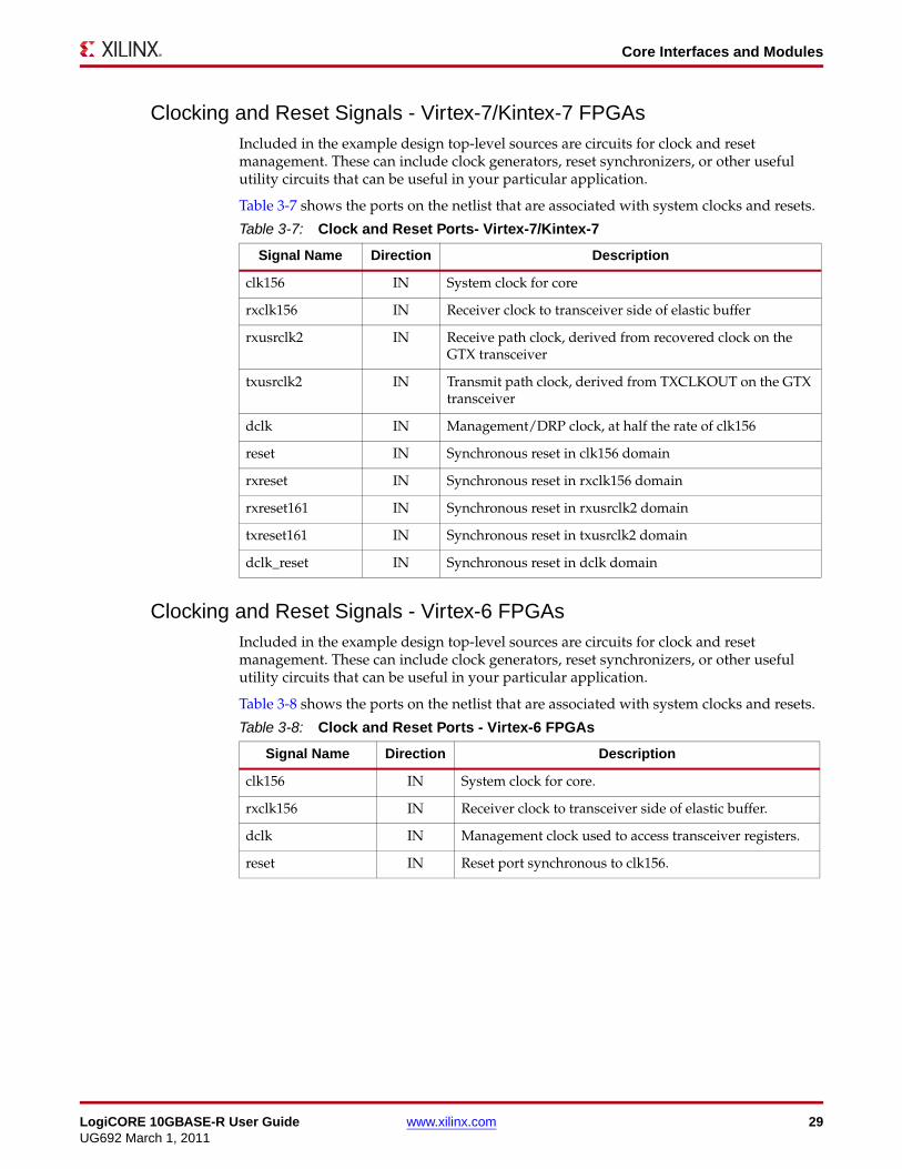
Clocking and Reset Signals - Virtex-7/Kintex-7 FPGAsIncluded in the example design top-level sources are circuits for clock and reset management. These can include clock generators, reset synchronizers, or other useful utility circuits that can be useful in your particular application.
Table 3-7 shows the ports on the netlist that are associated with system clocks and resets.
Signal Name Direction Description
clk156 System clock for core
rxclk156 Receiver clock to transceiver side of elastic buffer
rxusrclk2 Receive path clock, derived from recovered clock on the GTX transceiver
txusrclk2 Transmit path clock, derived from TXCLKOUT on the GTX transceiver
dclk Management/DRP clock, at half the rate of clk156
reset Synchronous reset in clk156 domain
rxreset Synchronous reset in rxclk156 domain
rxreset161 Synchronous reset in rxusrclk2 domain
txreset161 Synchronous reset in txusrclk2 domain
dclk_reset Synchronous reset in dclk domain
Clocking and Reset Signals - Virtex-6 FPGAsIncluded in the example design top-level sources are circuits for clock and reset management. These can include clock generators, reset synchronizers, or other useful utility circuits that can be useful in your particular application.
Table 3-8 shows the ports on the netlist that are associated with system clocks and resets.
Signal Name Direction Description
clk156 System clock for core.
rxclk156 Receiver clock to transceiver side of elastic buffer.
dclk Management clock used to access transceiver registers.
reset Reset port synchronous to clk156.
Table 3-7: Clock and Reset Ports- Virtex-7/Kintex-7
IN
IN
IN
IN
IN
IN
IN
IN
IN
IN
Table 3-8: Clock and Reset Ports - Virtex-6 FPGAs
IN
IN
IN
IN
LogiCORE 10GBASE-R User Guide www.xilinx.com 29UG692 March 1, 2011
Chapter 3: Core Architecture
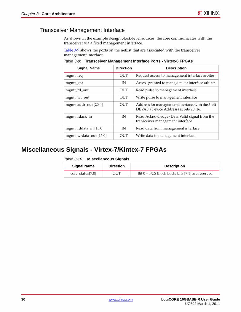
Transceiver Management Interface As shown in the example design block-level sources, the core communicates with the transceiver via a fixed management interface.
Table 3-9 shows the ports on the netlist that are associated with the transceiver management interface.
Signal Name Direction Description
mgmt_req Request access to management interface arbiter
mgmt_gnt Access granted to management interface arbiter
mgmt_rd_out Read pulse to management interface
mgmt_wr_out Write pulse to management interface
mgmt_addr_out [20:0] Address for management interface, with the 5-bit DEVAD (Device Address) at bits 20..16.
mgmt_rdack_in Read Acknowledge/Data Valid signal from the transceiver management interface
mgmt_rddata_in [15:0] Read data from management interface
mgmt_wrdata_out [15:0] Write data to management interface
Miscellaneous Signals - Virtex-7/Kintex-7 FPGAs
Table 3-9: Transceiver Management Interface Ports - Virtex-6 FPGAs
OUT
IN
OUT
OUT
OUT
IN
IN
OUT
Table 3-10: Miscellaneous Signals
Signal Name Direction Description
core_status[7:0] OUT Bit 0 = PCS Block Lock, Bits [7:1] are reserved
30 www.xilinx.com LogiCORE 10GBASE-R User GuideUG692 March 1, 2011
Chapter 4
Customizing and Generating the Core
The 10GBASE-R core is generated using the Xilinx® CORE Generator™ system. This chapter describes how to customize the 10GBASE-R core to your requirements and then generate the core netlist.
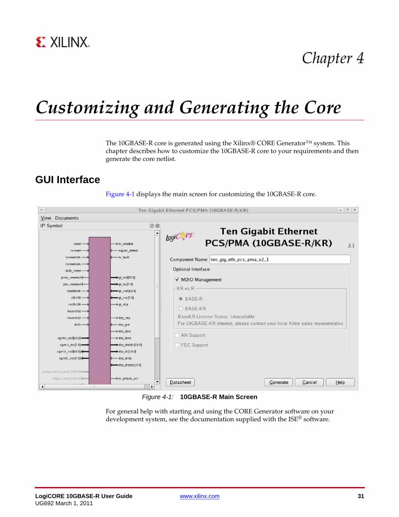
GUI InterfaceFigure 4-1 displays the main screen for customizing the 10GBASE-R core.
For general help with starting and using the CORE Generator software on your development system, see the documentation supplied with the ISE® software.
X-Ref Target - Figure 4-1
Figure 4-1: 10GBASE-R Main Screen
LogiCORE 10GBASE-R User Guide www.xilinx.com 31UG692 March 1, 2011
Chapter 4: Customizing and Generating the Core
Component NameThe component name is used as the base name of the output files generated for the core. Names must begin with a letter and must be composed from the following characters: a through z, 0 through 9 and “_” (underscore).
MDIO ManagementSelect this option to implement the MDIO interface for managing the core. Deselect the option to remove the MDIO interface and expose a simple bit vector to manage the core.
The default is to implement the MDIO interface.
Parameter Values in the XCO FileXCO files contain parameterization information for an instance of a core; an XCO file is created when a core is generated and can be used to recreate a core. The text in an XCO file is case-insensitive.
Table 4-1 shows the XCO file parameters and values, and summarizes the GUI defaults. The following is an example extract from an XCO file:
SELECT Ten_Gigabit_Ethernet_PCS/PMA_(10GBASE-R/KR) family Xilinx,_Inc. 2.1CSET component_name = the_coreCSET mdio_management = trueGENERATE
Output GenerationThe output files generated from the CORE Generator software are placed in the project directory. The list of output files includes:
• The netlist files for the core
• XCO files
• Release notes and documentation
• An HDL example design
• Scripts to synthesize, implement and simulate the example design.
See Chapter 10, Detailed Example Design, for a complete description of the CORE Generator software output files and for details of the HDL example design.
Table 4-1: XCO File Values and Defaults
Parameter XCO File Values Defaults
component_name ASCII text starting with a letter and based upon the following character set: a...z, 0...9 and _
ten_gig_eth_pcs_pma_v2_1
mdio_management True, false True
32 www.xilinx.com LogiCORE 10GBASE-R User GuideUG692 March 1, 2011
Chapter 5
Designing with the Core
This chapter provides a general description of how to use the 10GBASE-R core in your designs and should be used in conjunction with Chapter 6, Interfacing to the Core, which describes specific core interfaces.
General Design GuidelinesThis section describes the steps required to turn a 10GBASE-R core into a fully-functioning design with user-application logic. It is important to realize that not all implementations require all of the design steps listed in this chapter. Follow the logic design guidelines in this manual carefully.
Use the Example Design as a Starting PointEach instance of the 10GBASE-R core created by the CORE Generator™ software is delivered with an example design that can be implemented in an FPGA and simulated. This design can be used as a starting point for your own design or can be used to sanity-check your application in the event of difficulty.
See the Chapter 10, Detailed Example Design, for information about using and customizing the example designs for the 10GBASE-R core.
Know the Degree of Difficulty10GBASE-R designs are challenging to implement in any technology, and the degree of difficulty is further influenced by:
• Maximum system clock frequency
• Targeted device architecture
• Nature of your application
All 10GBASE-R implementations need careful attention to system performance requirements. Pipelining, logic mapping, placement constraints, and logic duplication are all methods that help boost system performance.
Keep It RegisteredTo simplify timing and increase system performance in an FPGA design, keep all inputs and outputs registered between your application and the core. This means that all inputs and outputs from your application should come from, or connect to a flip-flop. While registering signals cannot be possible for all paths, it simplifies timing analysis and makes it easier for the Xilinx tools to place and route the design.
LogiCORE 10GBASE-R User Guide www.xilinx.com 33UG692 March 1, 2011
Chapter 5: Designing with the Core
Recognize Timing Critical SignalsThe UCF provided with the example design for the core identifies the critical signals and the timing constraints that should be applied. See Chapter 7, Constraining the Core for further information.
Use Supported Design FlowsThe core is synthesized in the CORE Generator software and is delivered to you as an NGC netlist. The example implementation scripts provided currently use XST as the synthesis tool for the HDL example design that is delivered with the core. Other synthesis tools can be used for your application logic; the core is always unknown to the synthesis tool and appears as a black box.
Post synthesis, only Xilinx® ISE® v13.1 software tools are supported.
Make Only Allowed ModificationsThe 10GBASE-R core is not user-modifiable. Do not make modifications as they can have adverse effects on system timing and protocol compliance. Supported user configurations of the 10GBASE-R core can only be made by selecting the options from within the CORE Generator software when the core is generated. See Chapter 4, Customizing and Generating the Core.
34 www.xilinx.com LogiCORE 10GBASE-R User GuideUG692 March 1, 2011
Chapter 6
Interfacing to the Core
This chapter describes how to connect to the data interfaces of the core and configuration and status interfaces of the 10GBASE-R core.
Data Interface: Internal Interfaces
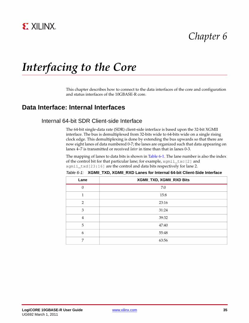
Internal 64-bit SDR Client-side InterfaceThe 64-bit single-data rate (SDR) client-side interface is based upon the 32-bit XGMII interface. The bus is demultiplexed from 32-bits wide to 64-bits wide on a single rising clock edge. This demultiplexing is done by extending the bus upwards so that there are now eight lanes of data numbered 0-7; the lanes are organized such that data appearing on lanes 4–7 is transmitted or received later in time than that in lanes 0-3.
The mapping of lanes to data bits is shown in Table 6-1. The lane number is also the index of the control bit for that particular lane; for example, xgmii_txc[2] and xgmii_txd[23:16] are the control and data bits respectively for lane 2.
Lane XGMII_TXD, XGMII_RXD Bits
Table 6-1: XGMII_TXD, XGMII_RXD Lanes for Internal 64-bit Client-Side Interface
0 7:0
1 15:8
2 23:16
3 31:24
4 39:32
5 47:40
6 55:48
7 63:56
LogiCORE 10GBASE-R User Guide www.xilinx.com 35UG692 March 1, 2011
Chapter 6: Interfacing to the Core
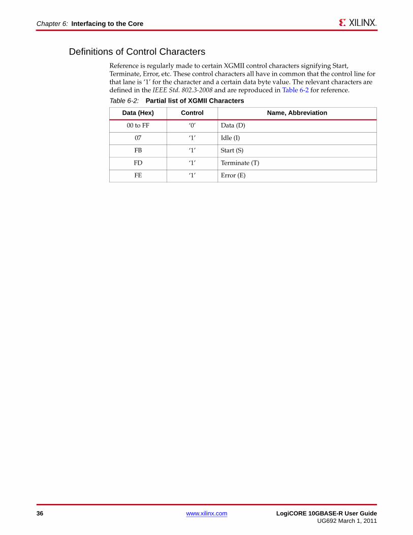
Definitions of Control CharactersReference is regularly made to certain XGMII control characters signifying Start, Terminate, Error, etc. These control characters all have in common that the control line for that lane is ‘1’ for the character and a certain data byte value. The relevant characters are defined in the IEEE Std. 802.3-2008 and are reproduced in Table 6-2 for reference.
Data (Hex) Control Name, Abbreviation
Data (D)
Idle (I)
Start (S)
Terminate (T)
Error (E)
Table 6-2: Partial list of XGMII Characters
00 to FF ‘0’
07 ‘1’
FB ‘1’
FD ‘1’
FE ‘1’
36 www.xilinx.com LogiCORE 10GBASE-R User GuideUG692 March 1, 2011
Interfacing to the Transmit Client Interface
Interfacing to the Transmit Client Interface
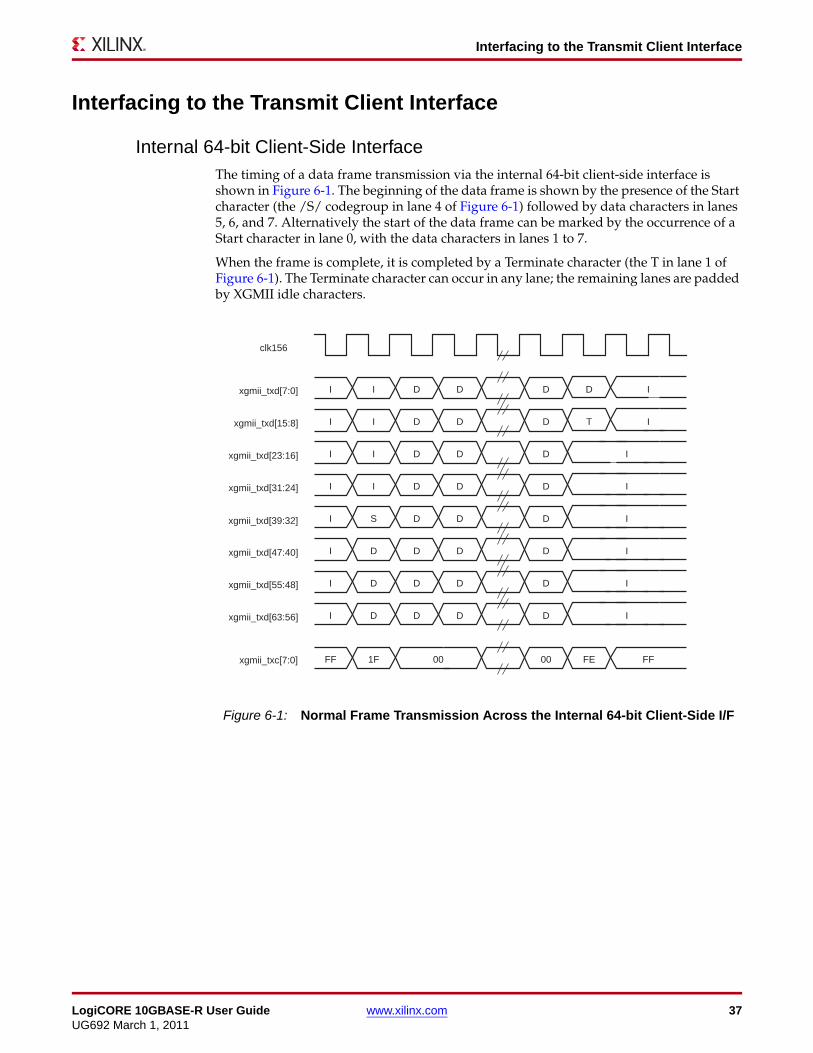
Internal 64-bit Client-Side InterfaceThe timing of a data frame transmission via the internal 64-bit client-side interface is shown in Figure 6-1. The beginning of the data frame is shown by the presence of the Start character (the /S/ codegroup in lane 4 of Figure 6-1) followed by data characters in lanes 5, 6, and 7. Alternatively the start of the data frame can be marked by the occurrence of a Start character in lane 0, with the data characters in lanes 1 to 7.
When the frame is complete, it is completed by a Terminate character (the T in lane 1 of Figure 6-1). The Terminate character can occur in any lane; the remaining lanes are padded by XGMII idle characters.X-Ref Target - Figure 6-1
Figure 6-1: Normal Frame Transmission Across the Internal 64-bit Client-Side I/F
clk156
xgmii_txd[7:0]
xgmii_txd[15:8]
xgmii_txd[23:16]
xgmii_txd[31:24]
xgmii_txd[39:32]
xgmii_txd[47:40]
xgmii_txd[55:48]
xgmii_txd[63:56]
xgmii_txc[7:0] FF00
D
D
D
D
D
D
D
D
D
D
D
D
D
D
D
D
00 FE
D
D
D
D
D
D
D
D
D
T
1F
I I
I I
I I
I I
I S
I D
I D
FF
I D
I
I
I
I
I
I
I
I
LogiCORE 10GBASE-R User Guide www.xilinx.com 37UG692 March 1, 2011
Chapter 6: Interfacing to the Core
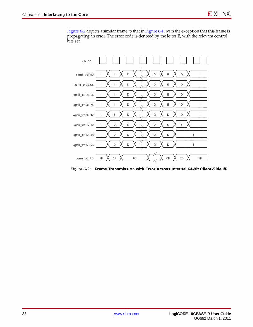
Figure 6-2 depicts a similar frame to that in Figure 6-1, with the exception that this frame is propagating an error. The error code is denoted by the letter E, with the relevant control bits set.X-Ref Target - Figure 6-2
Figure 6-2: Frame Transmission with Error Across Internal 64-bit Client-Side I/F
clk156
xgmii_txd[7:0]
xgmii_txd[15:8]
xgmii_txd[23:16]
xgmii_txd[31:24]
xgmii_txd[39:32]
xgmii_txd[47:40]
xgmii_txd[55:48]
xgmii_txd[63:56]
xgmii_txd[7:0] FF00
D
D
D
D
D
D
D
D
0F E0
E
E
E
E
D
D
D
D
1F
I I
I I
I I
I I
I S
I D
I D
FF
I D
I
I
I
I
D
D
D
D
D
D
D
D
D
D
D
D
D
T
I
I
I
I
38 www.xilinx.com LogiCORE 10GBASE-R User GuideUG692 March 1, 2011
Interfacing to the Receive Client Interface
Interfacing to the Receive Client Interface
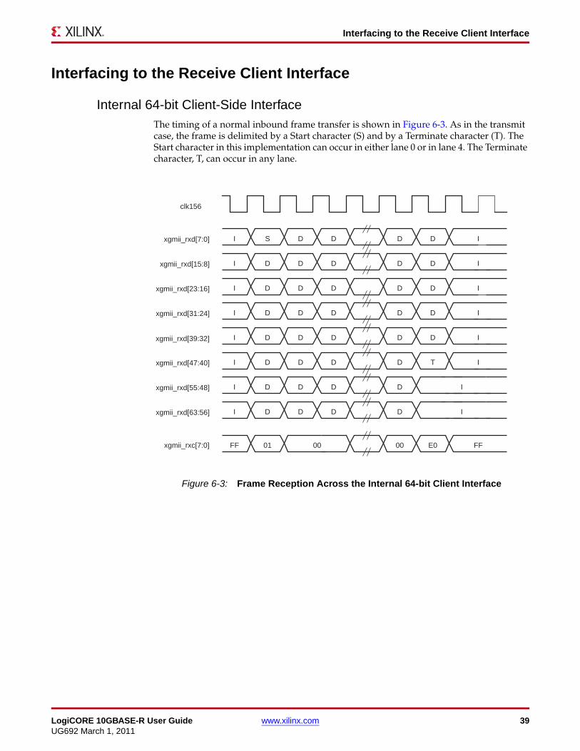
Internal 64-bit Client-Side InterfaceThe timing of a normal inbound frame transfer is shown in Figure 6-3. As in the transmit case, the frame is delimited by a Start character (S) and by a Terminate character (T). The Start character in this implementation can occur in either lane 0 or in lane 4. The Terminate character, T, can occur in any lane.X-Ref Target - Figure 6-3
Figure 6-3: Frame Reception Across the Internal 64-bit Client Interface
clk156
xgmii_rxd[7:0]
xgmii_rxd[15:8]
xgmii_rxd[23:16]
xgmii_rxd[31:24]
xgmii_rxd[39:32]
xgmii_rxd[47:40]
xgmii_rxd[55:48]
xgmii_rxd[63:56]
xgmii_rxc[7:0] FF00
D
D
D
D
D
D
D
D
D
D
D
D
D
D
D
D
00 E0
D
D
D
D
D
D
D
D
D
T
01
I S
I D
I D
I D
I D
I D
I D
FF
I D
I
I
I
I
D
D I
I
D
D I
I
LogiCORE 10GBASE-R User Guide www.xilinx.com 39UG692 March 1, 2011
Chapter 6: Interfacing to the Core
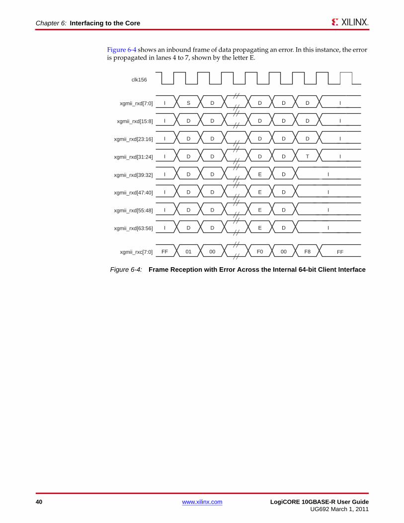
Figure 6-4 shows an inbound frame of data propagating an error. In this instance, the error is propagated in lanes 4 to 7, shown by the letter E.X-Ref Target - Figure 6-4
Figure 6-4: Frame Reception with Error Across the Internal 64-bit Client Interface
clk156
xgmii_rxd[7:0]
xgmii_rxd[15:8]
xgmii_rxd[23:16]
xgmii_rxd[31:24]
xgmii_rxd[39:32]
xgmii_rxd[47:40]
xgmii_rxd[55:48]
xgmii_rxd[63:56]
xgmii_rxc[7:0] FF
D
D
D
D
D
D
D
D
D
D
D
D
E
E
E
E
00 F8
D
D
D
D
D
D
D
D
01
I S
I D
I D
I D
I D
I D
I D
FF
I D
I
I
D
D I
I
D I
I
I
F000
T I
40 www.xilinx.com LogiCORE 10GBASE-R User GuideUG692 March 1, 2011
Interfacing to the Transceivers
Interfacing to the Transceivers
Virtex-7/Kintex-7 FPGAs
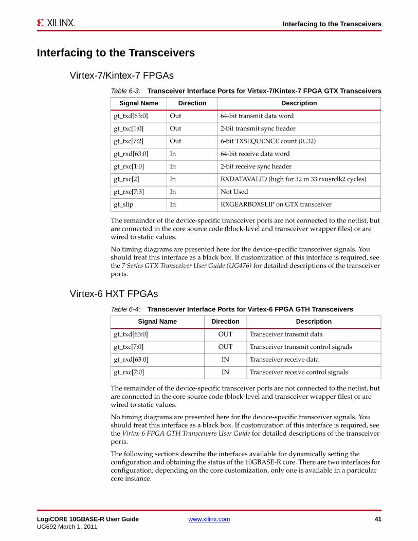
The remainder of the device-specific transceiver ports are not connected to the netlist, but are connected in the core source code (block-level and transceiver wrapper files) or are wired to static values.
No timing diagrams are presented here for the device-specific transceiver signals. You should treat this interface as a black box. If customization of this interface is required, see the 7 Series GTX Transceiver User Guide (UG476) for detailed descriptions of the transceiver ports.
Virtex-6 HXT FPGAs
The remainder of the device-specific transceiver ports are not connected to the netlist, but are connected in the core source code (block-level and transceiver wrapper files) or are wired to static values.
No timing diagrams are presented here for the device-specific transceiver signals. You should treat this interface as a black box. If customization of this interface is required, see the Virtex-6 FPGA GTH Transceivers User Guide for detailed descriptions of the transceiver ports.
The following sections describe the interfaces available for dynamically setting the configuration and obtaining the status of the 10GBASE-R core. There are two interfaces for configuration; depending on the core customization, only one is available in a particular core instance.
Table 6-3: Transceiver Interface Ports for Virtex-7/Kintex-7 FPGA GTX Transceivers
Signal Name Direction Description
gt_txd[63:0] Out 64-bit transmit data word
gt_txc[1:0] Out 2-bit transmit sync header
gt_txc[7:2] Out 6-bit TXSEQUENCE count (0..32)
gt_rxd[63:0] In 64-bit receive data word
gt_rxc[1:0] In 2-bit receive sync header
gt_rxc[2] In RXDATAVALID (high for 32 in 33 rxusrclk2 cycles)
gt_rxc[7:3] In Not Used
gt_slip In RXGEARBOXSLIP on GTX transceiver
Table 6-4: Transceiver Interface Ports for Virtex-6 FPGA GTH Transceivers
Signal Name Direction Description
gt_txd[63:0] OUT Transceiver transmit data
gt_txc[7:0] OUT Transceiver transmit control signals
gt_rxd[63:0] IN Transceiver receive data
gt_rxc[7:0] IN Transceiver receive control signals
LogiCORE 10GBASE-R User Guide www.xilinx.com 41UG692 March 1, 2011
Chapter 6: Interfacing to the Core
Configuration and Status InterfacesThis section describes the interfaces available for dynamically setting the configuration and obtaining the status of the 10GBASE-R core. There are two interfaces for configuration; depending on the core customization, only one is available in a particular core instance. The interfaces are:
• MDIO Interface, page 42
• Configuration and Status Vectors, page 72
MDIO InterfaceThe Management Data Input/Output (MDIO) interface is a simple, low-speed 2-wire interface for management of the 10GBASE-R core consisting of a clock signal and a bidirectional data signal. It is defined in clause 45 of IEEE Standard 802.3-2008.
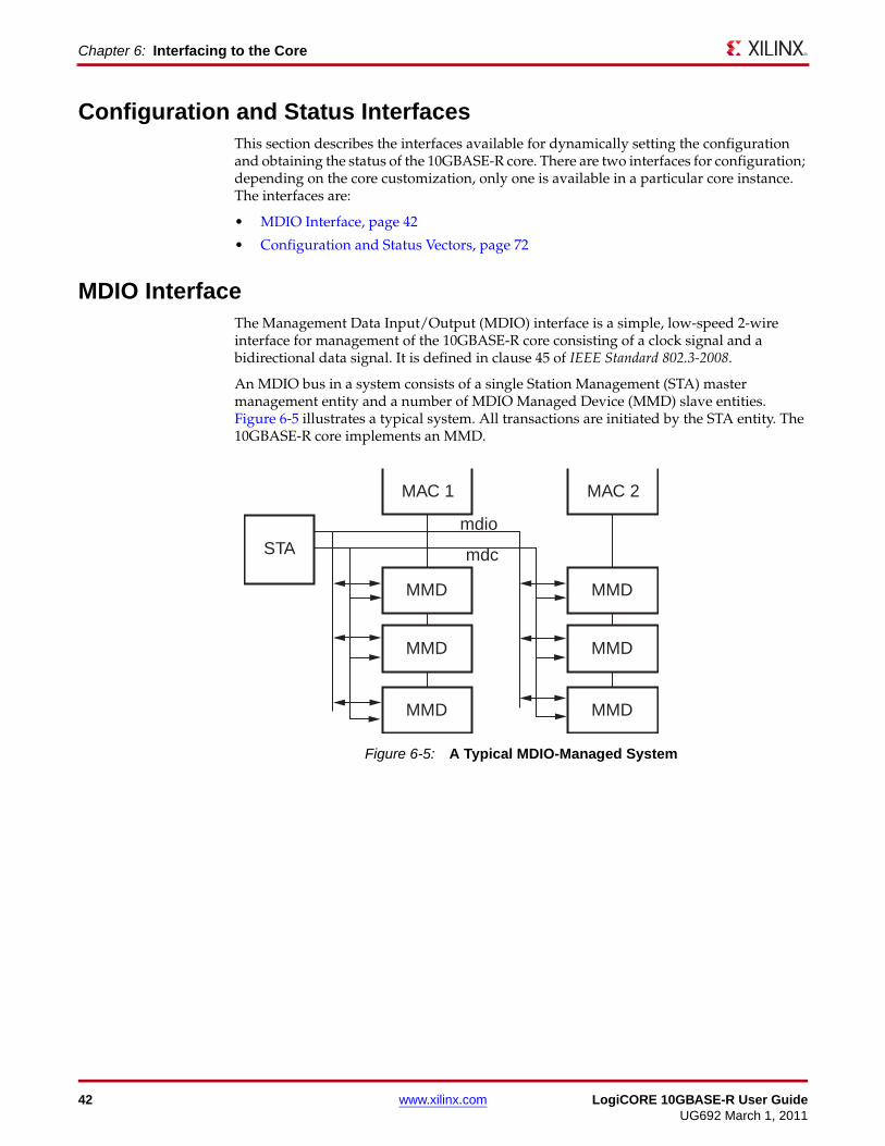
An MDIO bus in a system consists of a single Station Management (STA) master management entity and a number of MDIO Managed Device (MMD) slave entities. Figure 6-5 illustrates a typical system. All transactions are initiated by the STA entity. The 10GBASE-R core implements an MMD. X-Ref Target - Figure 6-5
Figure 6-5: A Typical MDIO-Managed System
MAC 1 MAC 2
STA mdc
mdio
MMD
MMD
MMD
MMD
MMD
MMD
42 www.xilinx.com LogiCORE 10GBASE-R User GuideUG692 March 1, 2011
MDIO Interface
MDIO PortsThe core ports associated with MDIO are shown in Table 6-5.
Signal Name Direction Description
mdc Management clock
mdio_in MDIO input
mdio_out MDIO output
mdio_tri MDIO 3-state. ‘1’ disconnects the output driver from the MDIO bus.
prtad[4:0] MDIO port address
If implemented, the MDIO interface is implemented as four unidirectional signals. These can be used to drive a 3-state buffer either in the FPGA SelectIO™ interface buffer or in a separate device.
The prtad[4:0] port sets the port address of the core instance. Multiple instances of the same core can be supported on the same MDIO bus by setting the prtad[4:0] to a unique value for each instance; the 10GBASE-R core ignores transactions with the PRTAD field set to a value other than that on its prtad[4:0] port.
MDIO TransactionsThe MDIO interface should be driven from a STA master according to the protocol defined in IEEE Std. 802.3-2008. An outline of each transaction type is described in the following sections. In these sections, these abbreviations apply:
• PRE: preamble
• ST: start
• OP: operation code
• PRTAD: port address
• DEVAD: device address
• TA: turnaround
DEVAD
The device address in this case will be either “00001” for the PMA device or “00011” for the PCS device, both of which are implemented in the GTH Transceiver. MDIO transactions with a DEVAD other than those two values are ignored.
Set Address Transaction
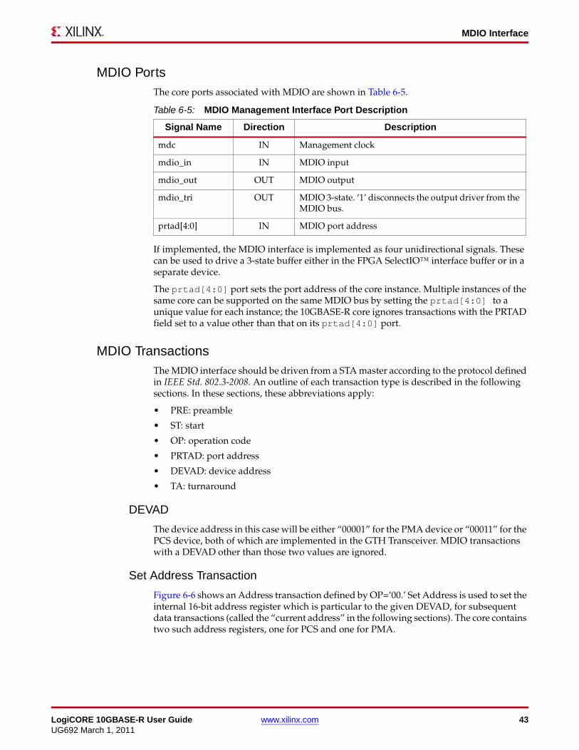
Figure 6-6 shows an Address transaction defined by OP=’00.’ Set Address is used to set the internal 16-bit address register which is particular to the given DEVAD, for subsequent data transactions (called the “current address” in the following sections). The core contains two such address registers, one for PCS and one for PMA.
Table 6-5: MDIO Management Interface Port Description
IN
IN
OUT
OUT
IN
LogiCORE 10GBASE-R User Guide www.xilinx.com 43UG692 March 1, 2011
Chapter 6: Interfacing to the Core
Write Transaction
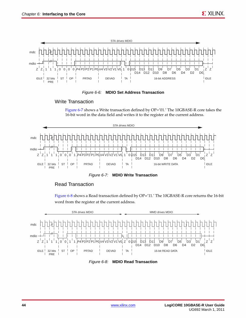
Figure 6-7 shows a Write transaction defined by OP=’01.’ The 10GBASE-R core takes the 16-bit word in the data field and writes it to the register at the current address.
Read Transaction
Figure 6-8 shows a Read transaction defined by OP=’11.’ The 10GBASE-R core returns the 16-bit
word from the register at the current address.
X-Ref Target - Figure 6-6
Figure 6-6: MDIO Set Address Transaction
Z1 1 1 0 0 0 P4 P3 P2 P1 P0 V4 V3 V2 V1 V0 1 0 D15D14
D13D12
D11D10
D9D8
D7D6
D5D4
D3D2
D1D0
0 ZZZ
mdc
mdio
IDLE IDLE32 bitsPRE
ST OP PRTAD DEVAD TA 16-bit ADDRESS
STA drives MDIO
X-Ref Target - Figure 6-7
Figure 6-7: MDIO Write Transaction
X-Ref Target - Figure 6-8
Figure 6-8: MDIO Read Transaction
Z1 1 1 0 0 1 P4 P3 P2 P1 P0 V4 V3 V2 V1 V0 1 0 D15D14
D13D12
D11D10
D9D8
D7D6
D5D4
D3D2
D1D0
0 ZZZ
mdc
mdio
IDLE IDLE32 bitsPRE
ST OP PRTAD DEVAD TA 16-bit WRITE DATA
STA drives MDIO
Z1 1 1 0 1 1 P4 P3 P2 P1 P0 V4 V3 V2 V1 V0 Z 0 D15D14
D13D12
D11D10
D9D8
D7D6
D5D4
D3D2
D1D0
0 ZZZ
mdc
mdio
IDLE IDLE32 bitsPRE
ST OP PRTAD DEVAD TA 16-bit READ DATA
STA drives MDIO MMD drives MDIO
44 www.xilinx.com LogiCORE 10GBASE-R User GuideUG692 March 1, 2011
MDIO Interface
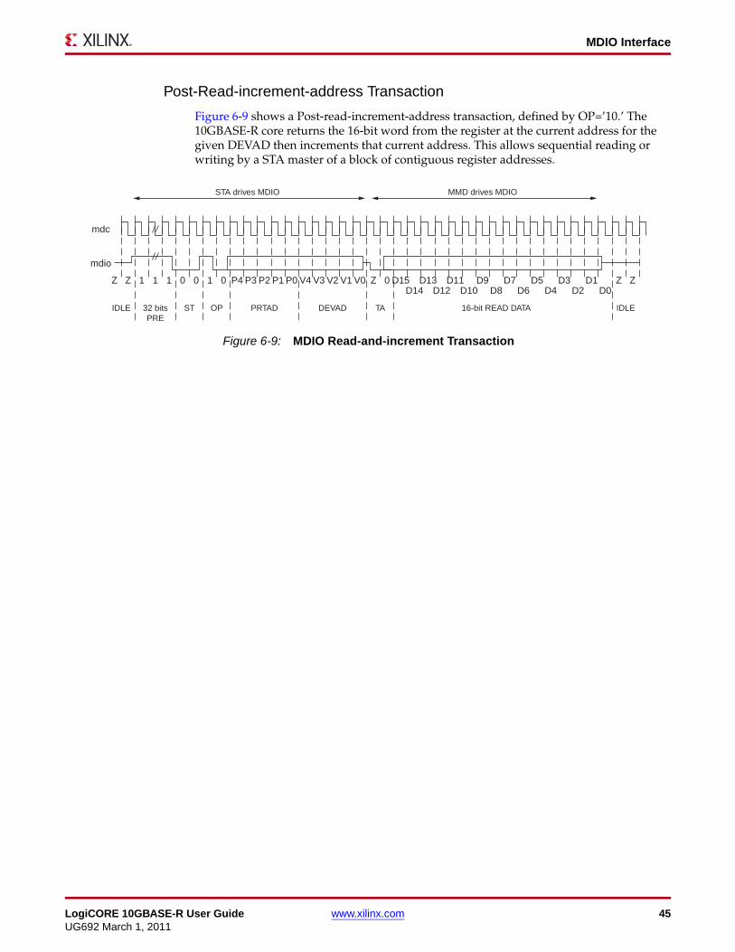
Post-Read-increment-address Transaction
Figure 6-9 shows a Post-read-increment-address transaction, defined by OP=’10.’ The 10GBASE-R core returns the 16-bit word from the register at the current address for the given DEVAD then increments that current address. This allows sequential reading or writing by a STA master of a block of contiguous register addresses.
X-Ref Target - Figure 6-9
Figure 6-9: MDIO Read-and-increment Transaction
Z1 1 1 0 1 0 P4 P3 P2 P1 P0 V4 V3 V2 V1 V0 Z 0 D15D14
D13D12
D11D10
D9D8
D7D6
D5D4
D3D2
D1D0
0 ZZZ
mdc
mdio
IDLE IDLE32 bitsPRE
ST OP PRTAD DEVAD TA 16-bit READ DATA
STA drives MDIO MMD drives MDIO
LogiCORE 10GBASE-R User Guide www.xilinx.com 45UG692 March 1, 2011
Chapter 6: Interfacing to the Core
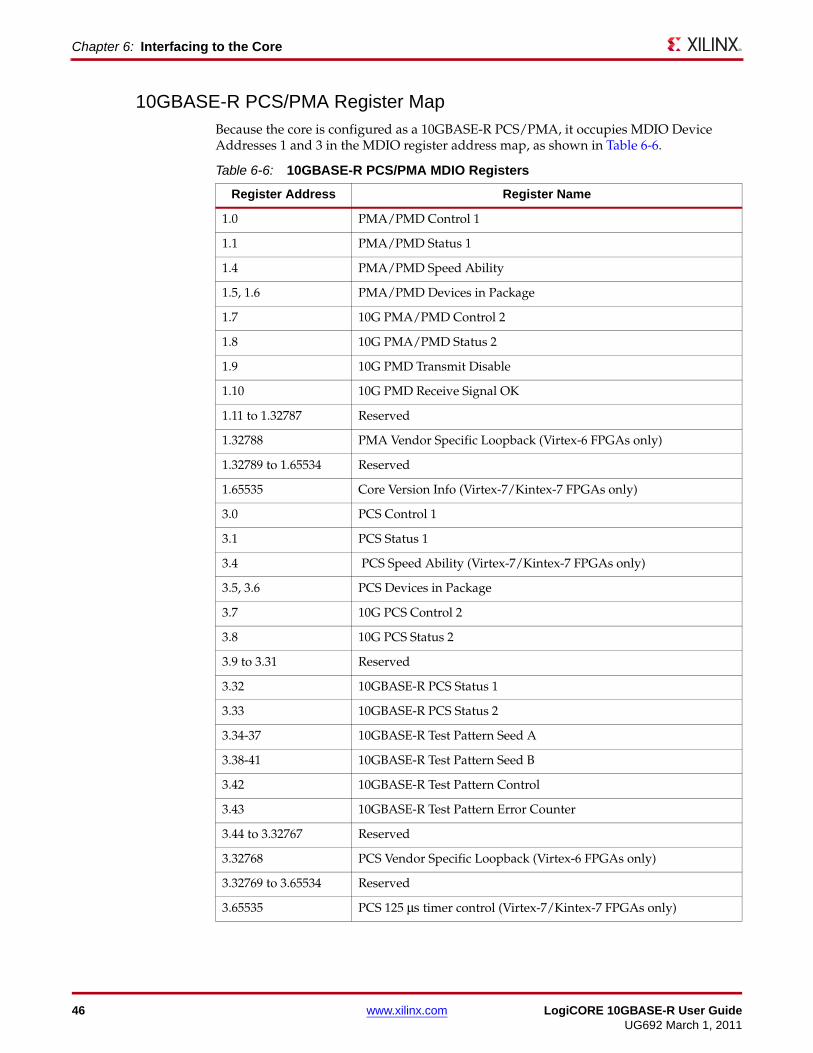
10GBASE-R PCS/PMA Register MapBecause the core is configured as a 10GBASE-R PCS/PMA, it occupies MDIO Device Addresses 1 and 3 in the MDIO register address map, as shown in Table 6-6.
Register Address Register Name
1.0 PMA/PMD Control 1
1.1 PMA/PMD Status 1
1.4 PMA/PMD Speed Ability
1.5, 1.6 PMA/PMD Devices in Package
1.7 10G PMA/PMD Control 2
1.8 10G PMA/PMD Status 2
1.9 10G PMD Transmit Disable
1.10 10G PMD Receive Signal OK
1.11 to 1.32787 Reserved
1.32788 PMA Vendor Specific Loopback (Virtex-6 FPGAs only)
1.32789 to 1.65534 Reserved
1.65535 Core Version Info (Virtex-7/Kintex-7 FPGAs only)
3.0 PCS Control 1
3.1 PCS Status 1
3.4 PCS Speed Ability (Virtex-7/Kintex-7 FPGAs only)
3.5, 3.6 PCS Devices in Package
3.7 10G PCS Control 2
3.8 10G PCS Status 2
3.9 to 3.31 Reserved
3.32 10GBASE-R PCS Status 1
3.33 10GBASE-R PCS Status 2
3.34-37 10GBASE-R Test Pattern Seed A
3.38-41 10GBASE-R Test Pattern Seed B
3.42 10GBASE-R Test Pattern Control
3.43 10GBASE-R Test Pattern Error Counter
3.44 to 3.32767 Reserved
3.32768 PCS Vendor Specific Loopback (Virtex-6 FPGAs only)
3.32769 to 3.65534 Reserved
3.65535 PCS 125 μs timer control (Virtex-7/Kintex-7 FPGAs only)
Table 6-6: 10GBASE-R PCS/PMA MDIO Registers
46 www.xilinx.com LogiCORE 10GBASE-R User GuideUG692 March 1, 2011
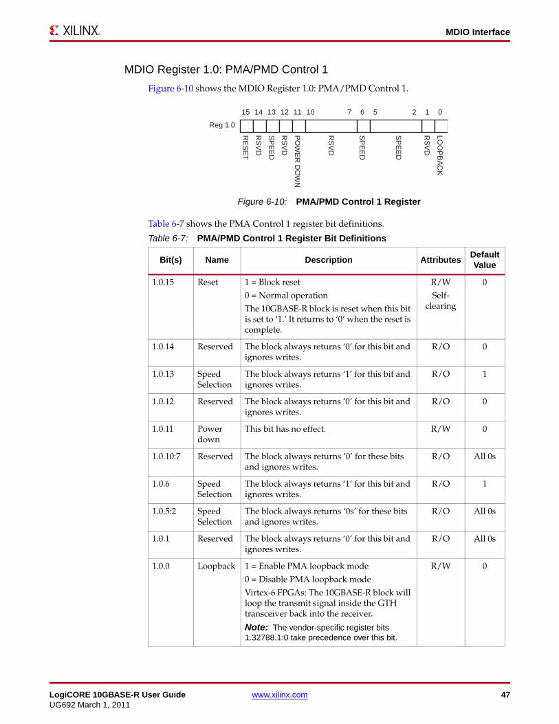
MDIO Interface
MDIO Register 1.0: PMA/PMD Control 1
Figure 6-10 shows the MDIO Register 1.0: PMA/PMD Control 1.
Table 6-7 shows the PMA Control 1 register bit definitions.
Bit(s) Name Description AttributesDefault Value
1.0.15 Reset 1 = Block reset
0 = Normal operation
The 10GBASE-R block is reset when this bit is set to ‘1.’ It returns to ‘0’ when the reset is complete.
1.0.14 Reserved The block always returns ‘0’ for this bit and ignores writes.
1.0.13 Speed Selection
The block always returns ‘1’ for this bit and ignores writes.
1.0.12 Reserved The block always returns ‘0’ for this bit and ignores writes.
1.0.11 Power down
This bit has no effect.
1.0.10:7 Reserved The block always returns ‘0’ for these bits and ignores writes.
1.0.6 Speed Selection
The block always returns ‘1’ for this bit and ignores writes.
1.0.5:2 Speed Selection
The block always returns ‘0s’ for these bits and ignores writes.
1.0.1 Reserved The block always returns ‘0’ for this bit and ignores writes.
1.0.0 Loopback 1 = Enable PMA loopback mode
0 = Disable PMA loopback mode
Virtex-6 FPGAs: The 10GBASE-R block will loop the transmit signal inside the GTH transceiver back into the receiver.
X-Ref Target - Figure 6-10
Figure 6-10: PMA/PMD Control 1 Register
Table 6-7: PMA/PMD Control 1 Register Bit Definitions
R/W
Self-clearing
0
R/O 0
R/O 1
R/O 0
R/W 0
R/O All 0s
R/O 1
R/O All 0s
R/O All 0s
Note: The vendor-specific register bits 1.32788.1:0 take precedence over this bit.
R/W 0
RE
SE
T
RS
VD
RS
VD
RS
VD
RS
VD
PO
WE
R D
OW
N
LOO
PB
AC
K
SP
EE
D
SP
EE
D
SP
EE
D
15 14 13 12 11 10 7 6 5 2 1 0
Reg 1.0
LogiCORE 10GBASE-R User Guide www.xilinx.com 47UG692 March 1, 2011
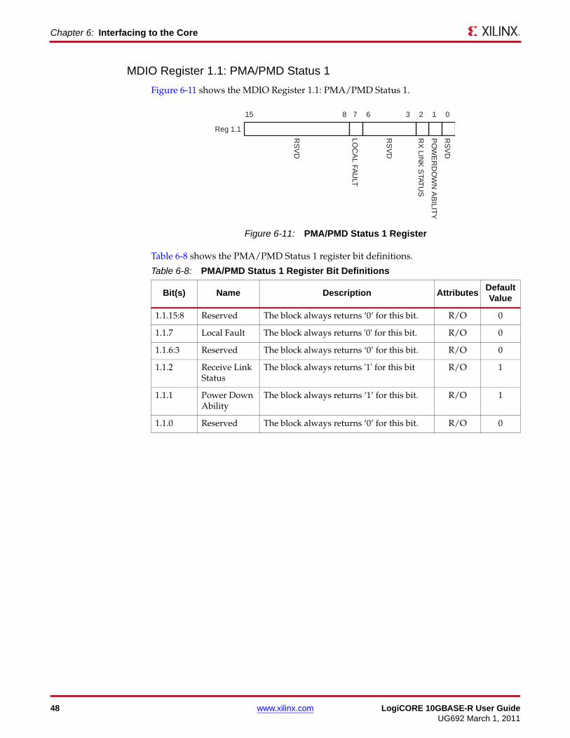
Chapter 6: Interfacing to the Core
MDIO Register 1.1: PMA/PMD Status 1
Figure 6-11 shows the MDIO Register 1.1: PMA/PMD Status 1.
Table 6-8 shows the PMA/PMD Status 1 register bit definitions.
Bit(s) Name Description AttributesDefault Value
1.1.15:8 Reserved The block always returns ‘0’ for this bit.
1.1.7 Local Fault The block always returns '0' for this bit.
1.1.6:3 Reserved The block always returns ‘0’ for this bit.
1.1.2 Receive Link Status
The block always returns '1' for this bit
1.1.1 Power Down Ability
The block always returns ‘1’ for this bit.
1.1.0 Reserved The block always returns ‘0’ for this bit.
X-Ref Target - Figure 6-11
Figure 6-11: PMA/PMD Status 1 Register
Table 6-8: PMA/PMD Status 1 Register Bit Definitions
R/O 0
R/O 0
R/O 0
R/O 1
R/O 1
R/O 0
RS
VD
RS
VD
RS
VD
LOC
AL FA
ULT
PO
WE
RD
OW
N A
BILIT
Y
RX
LINK
STAT
US
15 8 7 6 3 2 1 0
Reg 1.1
48 www.xilinx.com LogiCORE 10GBASE-R User GuideUG692 March 1, 2011
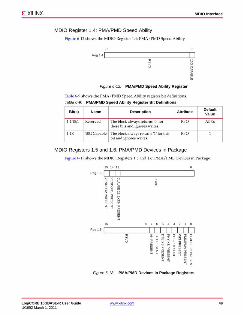
MDIO Interface
MDIO Register 1.4: PMA/PMD Speed Ability
Figure 6-12 shows the MDIO Register 1.4: PMA/PMD Speed Ability.
Table 6-9 shows the PMA/PMD Speed Ability register bit definitions.
Bit(s) Name Description AttributeDefault Value
1.4.15:1 Reserved The block always returns ‘0’ for these bits and ignores writes.
1.4.0 10G Capable The block always returns ‘1’ for this bit and ignores writes.
MDIO Registers 1.5 and 1.6: PMA/PMD Devices in Package
Figure 6-13 shows the MDIO Registers 1.5 and 1.6: PMA/PMD Devices in Package.
X-Ref Target - Figure 6-12
Figure 6-12: PMA/PMD Speed Ability Register
Table 6-9: PMA/PMD Speed Ability Register Bit Definitions
R/O All 0s
R/O 1
RS
VD
10G C
APA
BLE
15 0
Reg 1.4
X-Ref Target - Figure 6-13
Figure 6-13: PMA/PMD Devices in Package Registers
VE
ND
OR
2 PR
ES
EN
T
VE
ND
OR
1 PR
ES
EN
T
RS
VD
15 14 13 0
Reg 1.6
RS
VD
DT
E X
S P
RE
SE
NT
PH
Y X
S P
RE
SE
NT
PC
S P
RE
SE
NT
WIS
PR
ES
EN
T
PM
D/P
MA
PR
ES
EN
T
CLA
US
E 22 P
RE
SE
NT
15 0123456
Reg 1.5
78
TC
PR
ES
EN
T
AN
PR
ES
EN
T
CLA
US
E 22 E
XT.N
PR
ES
EN
T
LogiCORE 10GBASE-R User Guide www.xilinx.com 49UG692 March 1, 2011
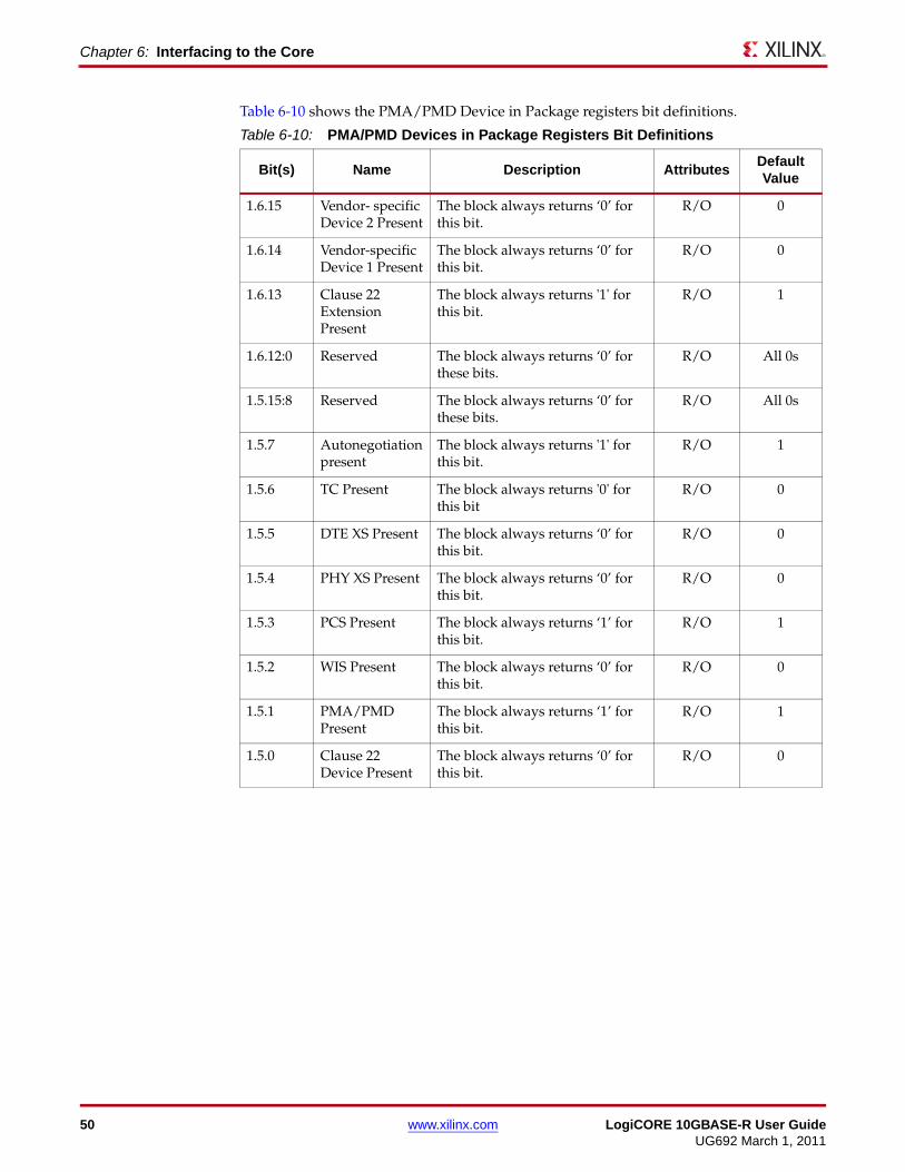
Chapter 6: Interfacing to the Core
Table 6-10 shows the PMA/PMD Device in Package registers bit definitions.
Bit(s) Name Description AttributesDefault Value
1.6.15 Vendor- specific Device 2 Present
The block always returns ‘0’ for this bit.
1.6.14 Vendor-specific Device 1 Present
The block always returns ‘0’ for this bit.
1.6.13 Clause 22 Extension Present
The block always returns '1' for this bit.
1.6.12:0 Reserved The block always returns ‘0’ for these bits.
1.5.15:8 Reserved The block always returns ‘0’ for these bits.
1.5.7 Autonegotiation present
The block always returns '1' for this bit.
1.5.6 TC Present The block always returns '0' for this bit
1.5.5 DTE XS Present The block always returns ‘0’ for this bit.
1.5.4 PHY XS Present The block always returns ‘0’ for this bit.
1.5.3 PCS Present The block always returns ‘1’ for this bit.
1.5.2 WIS Present The block always returns ‘0’ for this bit.
1.5.1 PMA/PMD Present
The block always returns ‘1’ for this bit.
1.5.0 Clause 22 Device Present
The block always returns ‘0’ for this bit.
Table 6-10: PMA/PMD Devices in Package Registers Bit Definitions
R/O 0
R/O 0
R/O 1
R/O All 0s
R/O All 0s
R/O 1
R/O 0
R/O 0
R/O 0
R/O 1
R/O 0
R/O 1
R/O 0
50 www.xilinx.com LogiCORE 10GBASE-R User GuideUG692 March 1, 2011
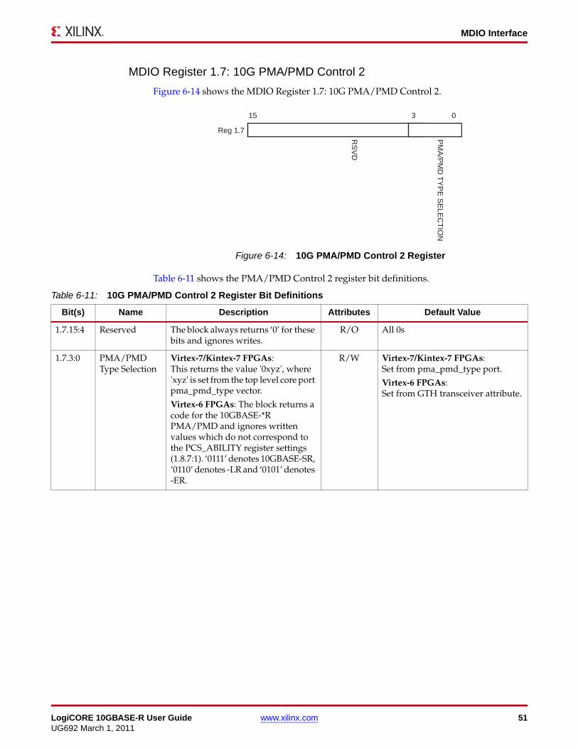
MDIO Interface
MDIO Register 1.7: 10G PMA/PMD Control 2
Figure 6-14 shows the MDIO Register 1.7: 10G PMA/PMD Control 2.
Table 6-11 shows the PMA/PMD Control 2 register bit definitions.
Bit(s) Name Description Attributes Default Value
1.7.15:4 Reserved The block always returns ‘0’ for these bits and ignores writes.
All 0s
1.7.3:0 PMA/PMD Type Selection
Virtex-7/Kintex-7 FPGAs: This returns the value '0xyz', where 'xyz' is set from the top level core port pma_pmd_type vector.
Virtex-6 FPGAs: The block returns a code for the 10GBASE-*R PMA/PMD and ignores written values which do not correspond to the PCS_ABILITY register settings (1.8.7:1). ‘0111’ denotes 10GBASE-SR, ‘0110’ denotes -LR and ‘0101’ denotes -ER.
Virtex-7/Kintex-7 FPGAs: Set from pma_pmd_type port.
Virtex-6 FPGAs: Set from GTH transceiver attribute.
X-Ref Target - Figure 6-14
Figure 6-14: 10G PMA/PMD Control 2 Register
RS
VD
PM
A/P
MD
TY
PE
SE
LEC
TIO
N
15 03
Reg 1.7
Table 6-11: 10G PMA/PMD Control 2 Register Bit Definitions
R/O
R/W
LogiCORE 10GBASE-R User Guide www.xilinx.com 51UG692 March 1, 2011
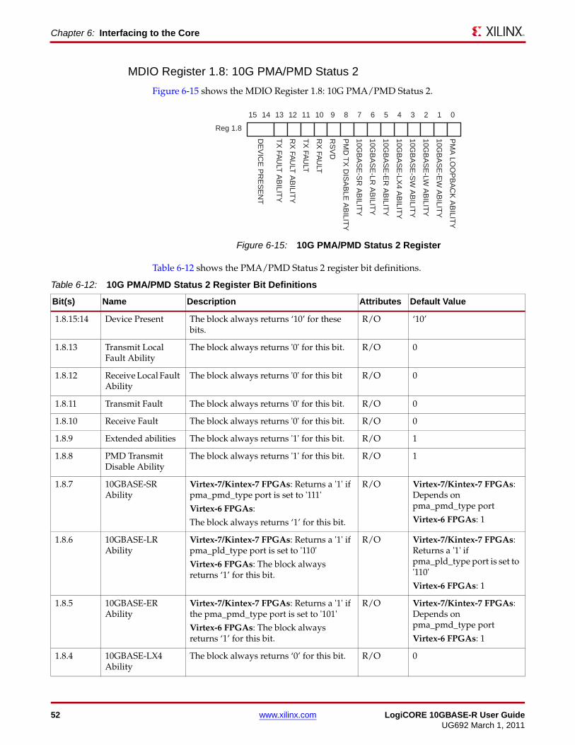
Chapter 6: Interfacing to the Core
MDIO Register 1.8: 10G PMA/PMD Status 2
Figure 6-15 shows the MDIO Register 1.8: 10G PMA/PMD Status 2.
Table 6-12 shows the PMA/PMD Status 2 register bit definitions.
X-Ref Target - Figure 6-15
Figure 6-15: 10G PMA/PMD Status 2 Register
DE
VIC
E P
RE
SE
NT
TX
FAU
LT A
BILIT
Y
RX
FAU
LT A
BILIT
Y
TX
FAU
LT
RX
FAU
LT
RS
VD
PM
D T
X D
ISA
BLE
AB
ILITY
10GB
AS
E-S
R A
BILIT
Y
10GB
AS
E-LR
AB
ILITY
10GB
AS
E-E
R A
BILIT
Y
10GB
AS
E-S
W A
BILIT
Y
10GB
AS
E-LW
AB
ILITY
10GB
AS
E-E
W A
BILIT
Y
PM
A LO
OP
BA
CK
AB
ILITY
10GB
AS
E-LX
4 AB
ILITY
15 14 58 7 613 12 11 10 9 24 3 1 0
Reg 1.8
Table 6-12: 10G PMA/PMD Status 2 Register Bit Definitions
Bit(s) Name Description Attributes Default Value
1.8.15:14 Device Present The block always returns ‘10’ for these bits.
R/O ‘10’
1.8.13 Transmit Local Fault Ability
The block always returns '0' for this bit. R/O 0
1.8.12 Receive Local Fault Ability
The block always returns '0' for this bit R/O 0
1.8.11 Transmit Fault The block always returns '0' for this bit. R/O 0
1.8.10 Receive Fault The block always returns '0' for this bit. R/O 0
1.8.9 Extended abilities The block always returns '1' for this bit. R/O 1
1.8.8 PMD Transmit Disable Ability
The block always returns '1' for this bit. R/O 1
1.8.7 10GBASE-SR Ability
Virtex-7/Kintex-7 FPGAs: Returns a '1' if pma_pmd_type port is set to '111'
Virtex-6 FPGAs:
The block always returns ‘1’ for this bit.
R/O Virtex-7/Kintex-7 FPGAs: Depends on pma_pmd_type port
Virtex-6 FPGAs: 1
1.8.6 10GBASE-LR Ability
Virtex-7/Kintex-7 FPGAs: Returns a '1' if pma_pld_type port is set to '110'
Virtex-6 FPGAs: The block always returns ‘1’ for this bit.
R/O Virtex-7/Kintex-7 FPGAs: Returns a '1' if pma_pld_type port is set to '110'
Virtex-6 FPGAs: 1
1.8.5 10GBASE-ER Ability
Virtex-7/Kintex-7 FPGAs: Returns a '1' if the pma_pmd_type port is set to '101'
Virtex-6 FPGAs: The block always returns ‘1’ for this bit.
R/O Virtex-7/Kintex-7 FPGAs: Depends on pma_pmd_type port
Virtex-6 FPGAs: 1
1.8.4 10GBASE-LX4 Ability
The block always returns ‘0’ for this bit. R/O 0
52 www.xilinx.com LogiCORE 10GBASE-R User GuideUG692 March 1, 2011
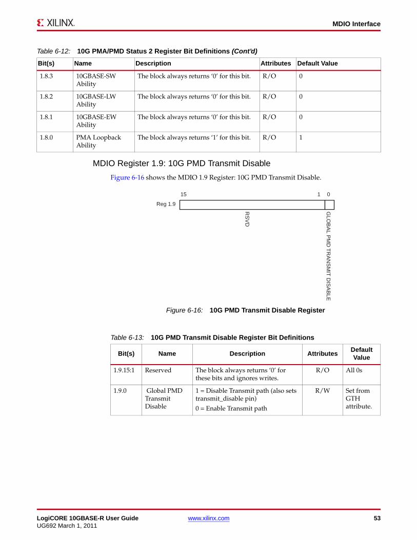
MDIO Interface
MDIO Register 1.9: 10G PMD Transmit Disable
Figure 6-16 shows the MDIO 1.9 Register: 10G PMD Transmit Disable.
Bit(s) Name Description AttributesDefault Value
1.9.15:1 Reserved The block always returns ‘0’ for these bits and ignores writes.
All 0s
1.9.0 Global PMD Transmit Disable
1 = Disable Transmit path (also sets transmit_disable pin)
0 = Enable Transmit path
Set from GTH attribute.
1.8.3 10GBASE-SW Ability
The block always returns ‘0’ for this bit. R/O 0
1.8.2 10GBASE-LW Ability
The block always returns ‘0’ for this bit. R/O 0
1.8.1 10GBASE-EW Ability
The block always returns ‘0’ for this bit. R/O 0
1.8.0 PMA Loopback Ability
The block always returns ‘1’ for this bit. R/O 1
Table 6-12: 10G PMA/PMD Status 2 Register Bit Definitions (Cont’d)
Bit(s) Name Description Attributes Default Value
X-Ref Target - Figure 6-16
Figure 6-16: 10G PMD Transmit Disable Register
Table 6-13: 10G PMD Transmit Disable Register Bit Definitions
R/O
R/W
RS
VD
GLO
BA
L PM
D T
RA
NS
MIT
DIS
AB
LE
15 1 0
Reg 1.9
LogiCORE 10GBASE-R User Guide www.xilinx.com 53UG692 March 1, 2011
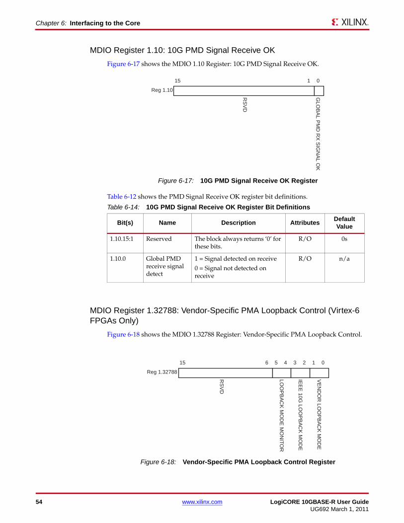
Chapter 6: Interfacing to the Core
MDIO Register 1.10: 10G PMD Signal Receive OK
Figure 6-17 shows the MDIO 1.10 Register: 10G PMD Signal Receive OK.
Table 6-12 shows the PMD Signal Receive OK register bit definitions.
Bit(s) Name Description AttributesDefault Value
1.10.15:1 Reserved The block always returns ‘0’ for these bits.
1.10.0 Global PMD receive signal detect
1 = Signal detected on receive
0 = Signal not detected on receive
MDIO Register 1.32788: Vendor-Specific PMA Loopback Control (Virtex-6 FPGAs Only)
Figure 6-18 shows the MDIO 1.32788 Register: Vendor-Specific PMA Loopback Control.
X-Ref Target - Figure 6-17
Figure 6-17: 10G PMD Signal Receive OK Register
Table 6-14: 10G PMD Signal Receive OK Register Bit Definitions
R/O 0s
R/O n/a
RS
VD
GLO
BA
L PM
D R
X S
IGN
AL O
K15 1 0
Reg 1.10
X-Ref Target - Figure 6-18
Figure 6-18: Vendor-Specific PMA Loopback Control Register
RS
VD
IEE
E 10G
LOO
PB
AC
K M
OD
E
VE
ND
OR
LOO
PB
AC
K M
OD
E
LOO
PB
AC
K M
OD
E M
ON
ITOR
15 56 24 3 1 0
Reg 1.32788
54 www.xilinx.com LogiCORE 10GBASE-R User GuideUG692 March 1, 2011
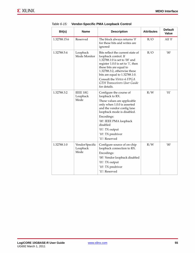
MDIO Interface
Bit(s) Name Description AttributesDefault Value
1.32788.15:6 Reserved The block always returns '0' for these bits and writes are ignored
1.32788.5:4 Loopback Mode Monitor
Bits reflect the current state of loopback control. If 1.32788.1:0 is set to '00' and register 1.0.0 is set to '1', then these bits are equal to 1.32788.3:2, otherwise these bits are equal to 1.32788.1:0.
Consult the Virtex-6 FPGA GTH Transceivers User Guide for details.
1.32788.3:2 IEEE 10G Loopback Mode
Configure the course of loopback to RX.
These values are applicable only when 1.0.0 is asserted and the vendor config lane loopback mode is disabled.
Encodings:
'00': IEEE PMA loopback disabled
'01': TX output
'10': TX predriver
'11': Reserved
1.32788.1:0 Vendor Specific Loopback Mode
Configure source of on-chip loopback connection to RX.
Encodings:
'00': Vendor loopback disabled
'01': TX output
'10': TX predriver
'11': Reserved
Table 6-15: Vendor-Specific PMA Loopback Control
R/O All '0'
R/O '00'
R/W '01'
R/W '00'
LogiCORE 10GBASE-R User Guide www.xilinx.com 55UG692 March 1, 2011
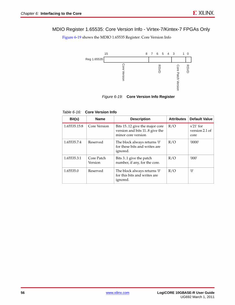
Chapter 6: Interfacing to the Core
MDIO Register 1.65535: Core Version Info - Virtex-7/Kintex-7 FPGAs Only
Figure 6-19 shows the MDIO 1.65535 Register: Core Version Info
Bit(s) Name Description Attributes Default Value
1.65535.15:8 Core Version Bits 15..12 give the major core version and bits 11..8 give the minor core version
R/O x'21' for version 2.1 of core
1.65535.7:4 Reserved The block always returns '0' for these bits and writes are ignored.
R/O '0000'
1.65535.3:1 Core Patch Version
Bits 3..1 give the patch number, if any, for the core.
R/O '000'
1.65535.0 Reserved The block always returns '0' for this bits and writes are ignored.
R/O '0'
X-Ref Target - Figure 6-19
Figure 6-19: Core Version Info Register
Table 6-16: Core Version Info
RS
VD
Core V
ersion
15 78 46 5 3 0
Reg 1.65535
1
RS
VD
Core P
atch Version
56 www.xilinx.com LogiCORE 10GBASE-R User GuideUG692 March 1, 2011
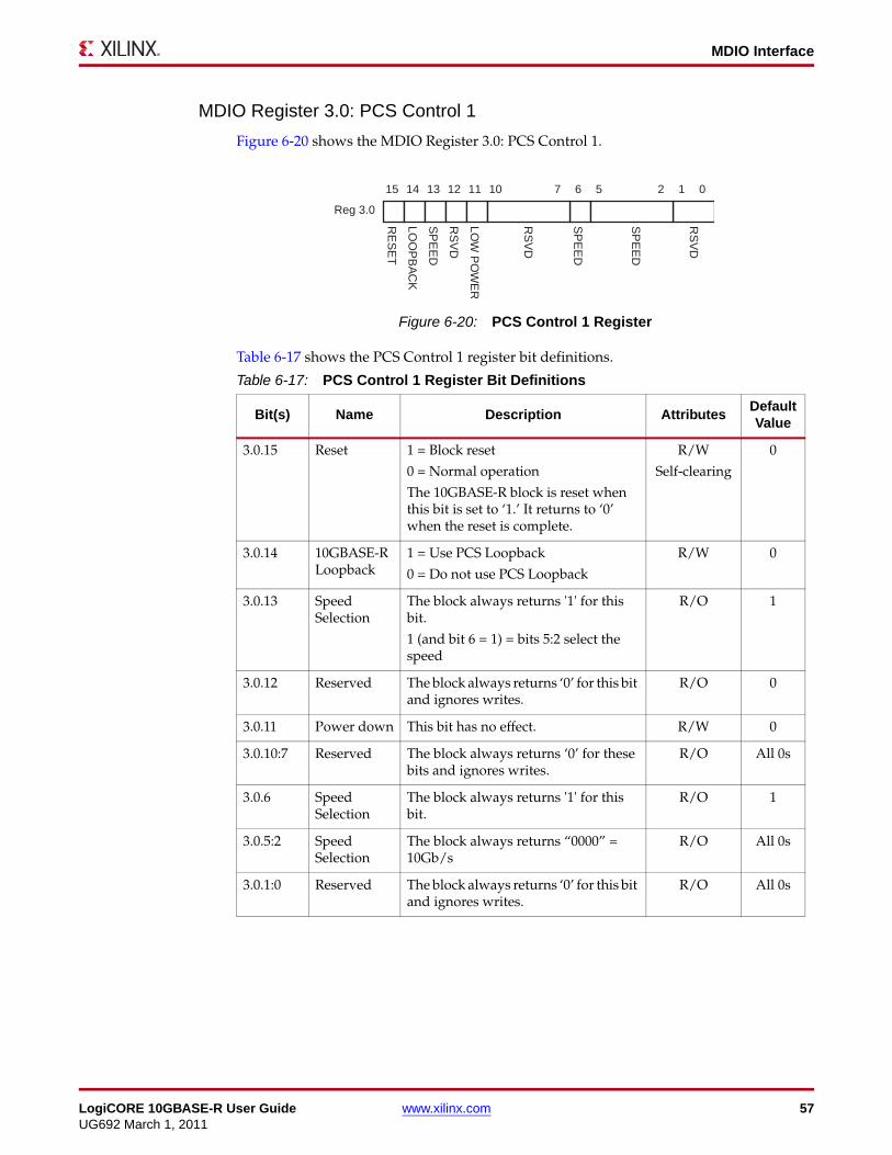
MDIO Interface
MDIO Register 3.0: PCS Control 1
Figure 6-20 shows the MDIO Register 3.0: PCS Control 1.
Table 6-17 shows the PCS Control 1 register bit definitions.
Bit(s) Name Description AttributesDefault Value
3.0.15 Reset 1 = Block reset
0 = Normal operation
The 10GBASE-R block is reset when this bit is set to ‘1.’ It returns to ‘0’ when the reset is complete.
3.0.14 10GBASE-R Loopback
1 = Use PCS Loopback
0 = Do not use PCS Loopback
3.0.13 Speed Selection
The block always returns '1' for this bit.
1 (and bit 6 = 1) = bits 5:2 select the speed
3.0.12 Reserved The block always returns ‘0’ for this bit and ignores writes.
3.0.11 Power down This bit has no effect.
3.0.10:7 Reserved The block always returns ‘0’ for these bits and ignores writes.
3.0.6 Speed Selection
The block always returns '1' for this bit.
3.0.5:2 Speed Selection
The block always returns “0000” = 10Gb/s
3.0.1:0 Reserved The block always returns ‘0’ for this bit and ignores writes.
X-Ref Target - Figure 6-20
Figure 6-20: PCS Control 1 Register
Table 6-17: PCS Control 1 Register Bit Definitions
R/W
Self-clearing
0
R/W 0
R/O 1
R/O 0
R/W 0
R/O All 0s
R/O 1
R/O All 0s
R/O All 0s
RE
SE
T
LOO
PB
AC
K
RS
VD
RS
VD
RS
VD
LOW
PO
WE
R
SP
EE
D
SP
EE
D
SP
EE
D
15 14 13 12 11 10 7 6 5 2 1 0
Reg 3.0
LogiCORE 10GBASE-R User Guide www.xilinx.com 57UG692 March 1, 2011
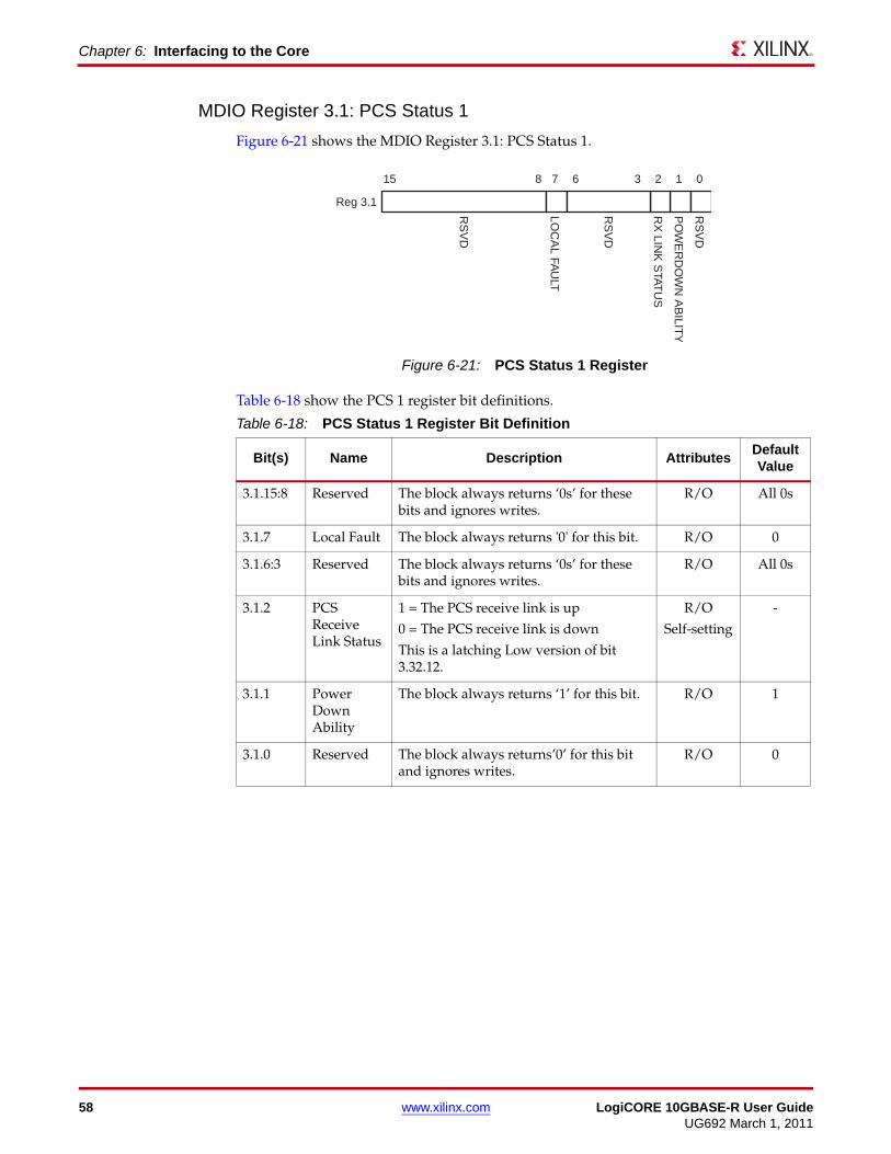
Chapter 6: Interfacing to the Core
MDIO Register 3.1: PCS Status 1
Figure 6-21 shows the MDIO Register 3.1: PCS Status 1.
Table 6-18 show the PCS 1 register bit definitions.
Bit(s) Name Description AttributesDefault Value
3.1.15:8 Reserved The block always returns ‘0s’ for these bits and ignores writes.
3.1.7 Local Fault The block always returns '0' for this bit.
3.1.6:3 Reserved The block always returns ‘0s’ for these bits and ignores writes.
3.1.2 PCS Receive Link Status
1 = The PCS receive link is up
0 = The PCS receive link is down
This is a latching Low version of bit 3.32.12.
3.1.1 Power Down Ability
The block always returns ‘1’ for this bit.
3.1.0 Reserved The block always returns’0’ for this bit and ignores writes.
X-Ref Target - Figure 6-21
Figure 6-21: PCS Status 1 Register
Table 6-18: PCS Status 1 Register Bit Definition
R/O All 0s
R/O 0
R/O All 0s
R/O
Self-setting
-
R/O 1
R/O 0
RS
VD
RS
VD
RS
VD
LOC
AL FA
ULT
PO
WE
RD
OW
N A
BILIT
Y
RX
LINK
STAT
US
15 8 7 6 3 2 1 0
Reg 3.1
58 www.xilinx.com LogiCORE 10GBASE-R User GuideUG692 March 1, 2011
MDIO Interface
MDIO Registers 3.5 and 3.6: PCS Devices in Package
Figure 6-22 shows the MDIO Registers 3.5 and 3.6: PCS Devices in Package.
Table 6-19 shows the PCS Devices in Package registers bit definitions.
X-Ref Target - Figure 6-22
Figure 6-22: PCS Devices in Package Registers
Table 6-19: PCS Devices in Package Registers Bit Definitions
Bit(s) Name Description AttributesDefault Value
3.6.15 Vendor-specific Device 2 Present
The block always returns ’0’ for this bit.
R/O 0
3.6.14 Vendor- specific Device 1 Present
The block always returns ’0’ for this bit.
R/O 0
3.6.12:0 Reserved The block always returns ’0’ for these bits.
R/O All 0s
3.6.13 Clause 22 extension present
The block always returns '1' for this bit.
R/O 1
3.5.15:8 Reserved The block always returns ’0’ for these bits.
R/O All 0s
3.5.7 Auto Negotiation Present
The block always returns’1’ for this bit.
R/O 1
3.5.6 TC present The block always returns’0’ for this bit.
R/O 0
VE
ND
OR
2 PR
ES
EN
T
VE
ND
OR
1 PR
ES
EN
T
RS
VD
15 14 13 0
Reg 3.6
RS
VD
DT
E X
S P
RE
SE
NT
PH
Y X
S P
RE
SE
NT
PC
S P
RE
SE
NT
WIS
PR
ES
EN
T
PM
D/P
MA
PR
ES
EN
T
CLA
US
E 22 P
RE
SE
NT
15 0123456
Reg 3.5
8 7
AN
PR
ES
EN
T
TC
PR
ES
EN
T
CLA
US
E 22 E
XT.N
PR
ES
EN
T
LogiCORE 10GBASE-R User Guide www.xilinx.com 59UG692 March 1, 2011
Chapter 6: Interfacing to the Core
MDIO Register 3.7: 10G PCS Control 2
Figure 6-23 shows the MDIO Register 3.7: 10G PCS Control 2.
Table 6-20 shows the 10 G PCS Control 2 register bit definitions.
Bit(s) Name Description AttributesDefault Value
3.7.15:2 Reserved The block always returns ’0’ for these bits and ignores writes.
3.7.1:0 PCS Type Selection
“00” = Select 10GBASE-R PCS type. Any other value written to this register are ignored.
3.5.5 PHY XS Present The block always returns ’0’ for this bit.
R/O 0
3.5.4 PHY XS Present The block always returns ’0’ for this bit.
R/O 0
3.5.3 PCS Present The block always returns ’1’ for this bit.
R/O 1
3.5.2 WIS Present The block always returns ’0’ for this bit.
R/O 0
3.5.1 PMA/PMD Present
The block always returns ’1’ for this bit.
R/O 1
3.5.0 Clause 22 device present
The block always returns ’0’ for this bit.
R/O 0
Table 6-19: PCS Devices in Package Registers Bit Definitions (Cont’d)
Bit(s) Name Description AttributesDefault Value
X-Ref Target - Figure 6-23
Figure 6-23: 10G PCS Control 2 Register
Table 6-20: 10G PCS Control 2 Register Bit Definitions
R/O All 0s
R/W 00
RS
VD
PC
S T
YP
E S
ELE
CT
ION
15 02 1
Reg 3.7
60 www.xilinx.com LogiCORE 10GBASE-R User GuideUG692 March 1, 2011
MDIO Interface
MDIO Register 3.8: 10G PCS Status 2
Figure 6-24 shows the MDIO Register 3.8: 10G PCS Status 2.
Table 6-21 shows the 10G PCS Status 2 register bit definitions.
Bit(s) Name Description AttributesDefault Value
3.8.15:14 Device present
The block always returns “10.”
3.8.13:12 Reserved The block always returns ’0’ for these bits.
3.8.11 Transmit local fault
The block always returns '0' for this bit.
3.8.10 Receive local fault
The block always returns '0' for this bit.
3.8.9:3 Reserved The block always returns ’0’ for these bits.
3.8.2 10GBASE-W Capable
The block always returns '0' for this bit.
3.8.1 10GBASE-X Capable
The block always returns '0' for this bit.
3.8.0 10GBASE-R Capable
The block always returns '1' for this bit.
X-Ref Target - Figure 6-24
Figure 6-24: 10G PCS Status 2 Register
Table 6-21: 10G PCS Status 2 Register Bit Definitions
R/O “10”
R/O All 0s
R/O 0
R/O 0
R/O All 0s
R/O 0
R/O 0
R/O 1
DE
VIC
E P
RE
SE
NT
RS
VD
TX
FAU
LT
RX
FAU
LT
RS
VD
10GB
AS
E-W
AB
ILITY
10GB
AS
E-X
AB
ILITY
10GB
AS
E-R
AB
ILITY
15 14 13 12 11 10 9 23 1 0
Reg 3.8
LogiCORE 10GBASE-R User Guide www.xilinx.com 61UG692 March 1, 2011
Chapter 6: Interfacing to the Core
MDIO Register 3.32: 10GBASE-R Status 1
Figure 6-25 shows the MDIO Register 3.32: 10GBase-R Status 1
Table 6-22 shows the 10GBASE-R Status register bit definitions.
Bit(s) Name Description AttributesDefault Value
3.32.15:13 Reserved The block always returns ’0’ for these bits.
3.32.12 10GBASE-R Link Status
1 = 10GBASE-R receive is aligned;
0 = 10GBASE-R receive is not aligned.
3.32.11:3 Reserved The block always returns '0' for these bits.
3.32.2 PRBS31 Pattern Testing Ability
The block always returns '1' for this bit.
3.32.1 Hi BER 1 = RX showing hi-ber
0 = RX not showing hi ber
3.32.0 Block Lock 1 = RX is synchronized;
0 = RX is not synchronized.
X-Ref Target - Figure 6-25
Figure 6-25: 10GBASE-R Status Register 1
Table 6-22: 10GBASE-R Status Register 1 Bit Definitions
R/O All 0s
RO 0
R/O 0s
R/O 1
R/O 0
R/O 0
RS
VD
RS
VD
LINK
STAT
US
PR
BS
31 TE
ST
ING
AB
ILITY
HI_B
ER
BLO
CK
_LOC
K15 13 12 11 3 2 1 0
Reg 3.32
62 www.xilinx.com LogiCORE 10GBASE-R User GuideUG692 March 1, 2011
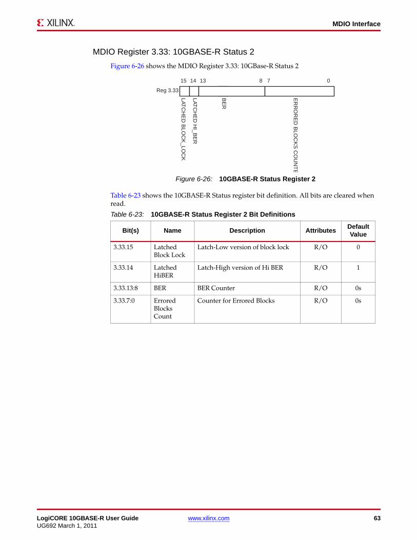
MDIO Interface
MDIO Register 3.33: 10GBASE-R Status 2
Figure 6-26 shows the MDIO Register 3.33: 10GBase-R Status 2
Table 6-23 shows the 10GBASE-R Status register bit definition. All bits are cleared when read.
Bit(s) Name Description AttributesDefault Value
3.33.15 Latched Block Lock
Latch-Low version of block lock
3.33.14 Latched HiBER
Latch-High version of Hi BER
3.33.13:8 BER BER Counter
3.33.7:0 Errored Blocks Count
Counter for Errored Blocks
X-Ref Target - Figure 6-26
Figure 6-26: 10GBASE-R Status Register 2
Table 6-23: 10GBASE-R Status Register 2 Bit Definitions
R/O 0
R/O 1
R/O 0s
R/O 0s
LATC
HE
D H
I_BE
R
BE
R
LATC
HE
D B
LOC
K_LO
CK
ER
RO
RE
D B
LOC
KS
CO
UN
TE
15 13 8 7 0
Reg 3.33
14
LogiCORE 10GBASE-R User Guide www.xilinx.com 63UG692 March 1, 2011
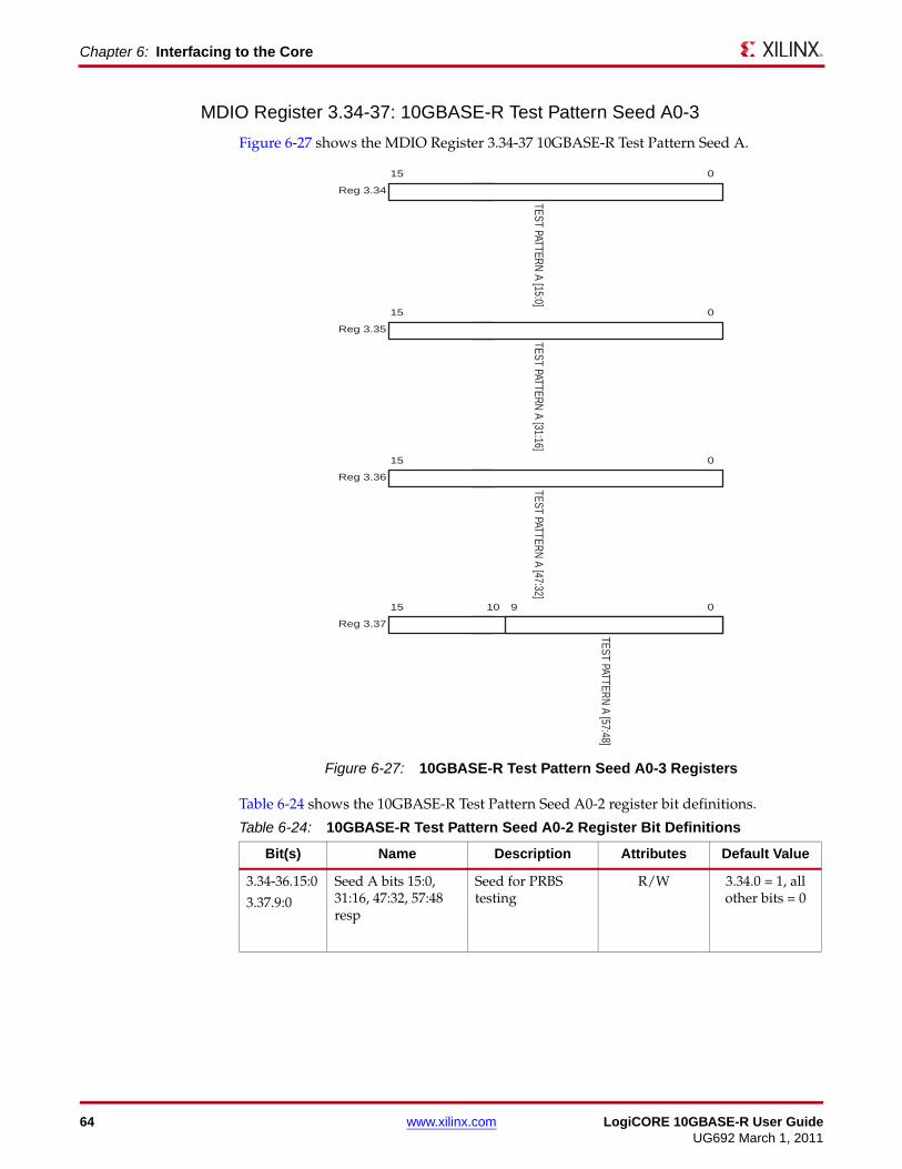
Chapter 6: Interfacing to the Core
MDIO Register 3.34-37: 10GBASE-R Test Pattern Seed A0-3
Figure 6-27 shows the MDIO Register 3.34-37 10GBASE-R Test Pattern Seed A.
Table 6-24 shows the 10GBASE-R Test Pattern Seed A0-2 register bit definitions.
Bit(s) Name Description Attributes Default Value
3.34-36.15:0
3.37.9:0
Seed A bits 15:0, 31:16, 47:32, 57:48 resp
Seed for PRBS testing
X-Ref Target - Figure 6-27
Figure 6-27: 10GBASE-R Test Pattern Seed A0-3 Registers
Table 6-24: 10GBASE-R Test Pattern Seed A0-2 Register Bit Definitions
R/W 3.34.0 = 1, all other bits = 0
TEST PATTERN A [15:0]
15 0
Reg 3.34
TEST PATTERN A [31:16]
15 0
Reg 3.35
TEST PATTERN A [47:32]
15 0
Reg 3.36
TEST PATTERN A [57:48]
15 0
Reg 3.37
10 9
64 www.xilinx.com LogiCORE 10GBASE-R User GuideUG692 March 1, 2011
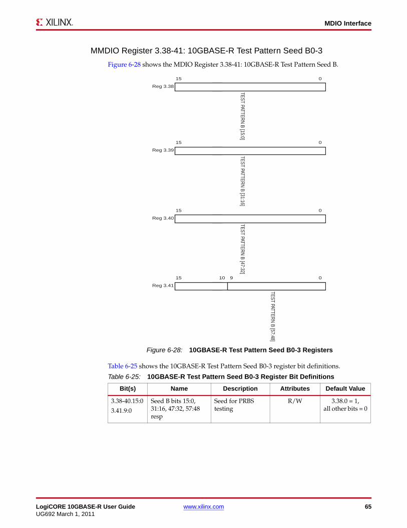
MDIO Interface
MMDIO Register 3.38-41: 10GBASE-R Test Pattern Seed B0-3
Figure 6-28 shows the MDIO Register 3.38-41: 10GBASE-R Test Pattern Seed B.
Table 6-25 shows the 10GBASE-R Test Pattern Seed B0-3 register bit definitions.
Bit(s) Name Description Attributes Default Value
3.38-40.15:0
3.41.9:0
Seed B bits 15:0, 31:16, 47:32, 57:48 resp
Seed for PRBS testing
X-Ref Target - Figure 6-28
Figure 6-28: 10GBASE-R Test Pattern Seed B0-3 Registers
Table 6-25: 10GBASE-R Test Pattern Seed B0-3 Register Bit Definitions
R/W 3.38.0 = 1, all other bits = 0
TEST PATTERN
B [15:0]
15 0
Reg 3.38
TEST PATTERN
B [31:16]
15 0
Reg 3.39
TEST PATTERN
B [47:32]
15 0
Reg 3.40
TEST PATTERN
B [57:48]
15 0
Reg 3.41
10 9
LogiCORE 10GBASE-R User Guide www.xilinx.com 65UG692 March 1, 2011
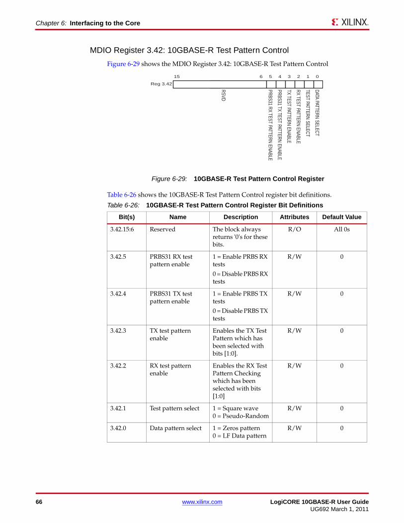
Chapter 6: Interfacing to the Core
MDIO Register 3.42: 10GBASE-R Test Pattern Control
Figure 6-29 shows the MDIO Register 3.42: 10GBASE-R Test Pattern Control
Table 6-26 shows the 10GBASE-R Test Pattern Control register bit definitions.
Bit(s) Name Description Attributes Default Value
3.42.15:6 Reserved The block always returns '0's for these bits.
3.42.5 PRBS31 RX test pattern enable
1 = Enable PRBS RX tests
0 = Disable PRBS RX tests
3.42.4 PRBS31 TX test pattern enable
1 = Enable PRBS TX tests
0 = Disable PRBS TX tests
3.42.3 TX test pattern enable
Enables the TX Test Pattern which has been selected with bits [1:0].
3.42.2 RX test pattern enable
Enables the RX Test Pattern Checking which has been selected with bits [1:0]
3.42.1 Test pattern select 1 = Square wave 0 = Pseudo-Random
3.42.0 Data pattern select 1 = Zeros pattern 0 = LF Data pattern
X-Ref Target - Figure 6-29
Figure 6-29: 10GBASE-R Test Pattern Control Register
Table 6-26: 10GBASE-R Test Pattern Control Register Bit Definitions
R/O All 0s
R/W 0
R/W 0
R/W 0
R/W 0
R/W 0
R/W 0
RSVD
15 0
Reg 3.42
6 5 4 3 2 1
PRBS31 RX TEST PATTERN ENABLE
PRBS31 TX TEST PATTERN ENABLE
TX TEST PATTERN ENABLE
RX TEST PATTERN ENABLE
TEST PATTERN SELECT
DATA PATTERN SELECT
66 www.xilinx.com LogiCORE 10GBASE-R User GuideUG692 March 1, 2011
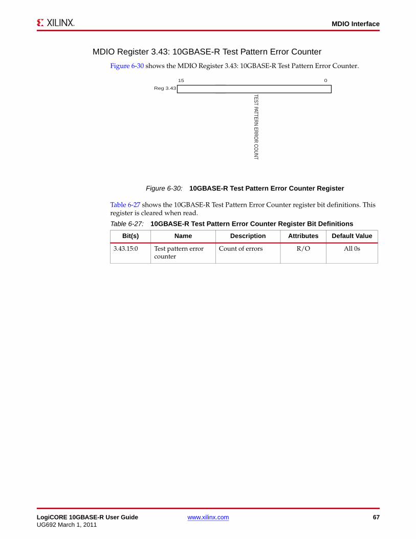
MDIO Interface
MDIO Register 3.43: 10GBASE-R Test Pattern Error Counter
Figure 6-30 shows the MDIO Register 3.43: 10GBASE-R Test Pattern Error Counter.
Table 6-27 shows the 10GBASE-R Test Pattern Error Counter register bit definitions. This register is cleared when read.
Bit(s) Name Description Attributes Default Value
3.43.15:0 Test pattern error counter
Count of errors
X-Ref Target - Figure 6-30
Figure 6-30: 10GBASE-R Test Pattern Error Counter Register
Table 6-27: 10GBASE-R Test Pattern Error Counter Register Bit Definitions
R/O All 0s
TEST PATTERN
ERRO
R C
OU
NT
15 0
Reg 3.43
LogiCORE 10GBASE-R User Guide www.xilinx.com 67UG692 March 1, 2011
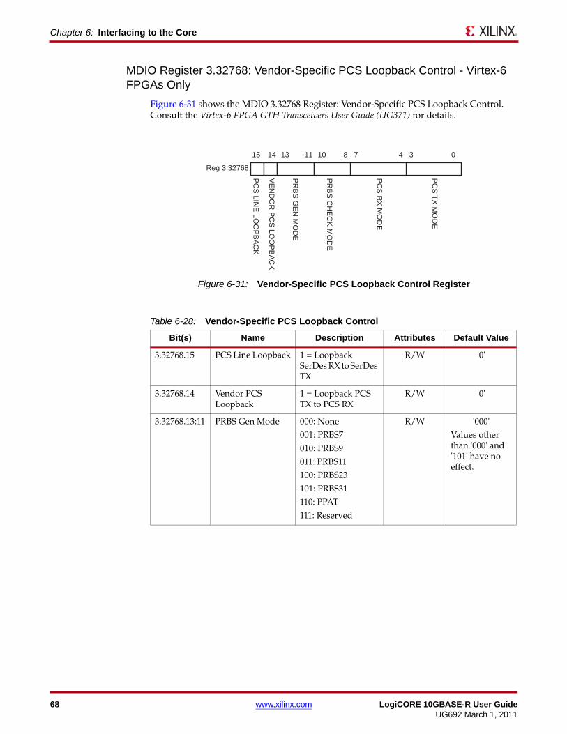
Chapter 6: Interfacing to the Core
MDIO Register 3.32768: Vendor-Specific PCS Loopback Control - Virtex-6 FPGAs Only
Figure 6-31 shows the MDIO 3.32768 Register: Vendor-Specific PCS Loopback Control. Consult the Virtex-6 FPGA GTH Transceivers User Guide (UG371) for details.
X-Ref Target - Figure 6-31
Figure 6-31: Vendor-Specific PCS Loopback Control Register
Table 6-28: Vendor-Specific PCS Loopback Control
Bit(s) Name Description Attributes Default Value
3.32768.15 PCS Line Loopback 1 = Loopback SerDes RX to SerDes TX
R/W '0'
3.32768.14 Vendor PCS Loopback
1 = Loopback PCS TX to PCS RX
R/W '0'
3.32768.13:11 PRBS Gen Mode 000: None
001: PRBS7
010: PRBS9
011: PRBS11
100: PRBS23
101: PRBS31
110: PPAT
111: Reserved
R/W '000'
Values other than '000' and '101' have no effect.
PC
S R
X M
OD
E
PC
S T
X M
OD
E
PR
BS
CH
EC
K M
OD
E
15 1011 48 7 3 0
Reg 3.32768
14 13
PC
S LIN
E LO
OP
BA
CK
VE
ND
OR
PC
S LO
OP
BA
CK
PR
BS
GE
N M
OD
E
68 www.xilinx.com LogiCORE 10GBASE-R User GuideUG692 March 1, 2011
MDIO Interface
1.32768.10:8 PRBS Check Mode 000: None
001: PRBS7
010: PRBS9
011: PRBS11
100: PRBS23
101: PRBS31
110: PPAT
111: Reserved
R/W '000
Values other than '000' and '101' have no effect.
3.32768.7:4 PCS RX Mode 0000: Zero
0001: 64/66b
0010: XAUI
0011: Reserved
0100: PCIE®
0101: PCIE-500 (fixed PCLK 500MHz)
0110: 8B/10B 8-bit
0111: 8B/10B 16-bit
1000: 8-bit raw data
1001: 10-bit raw data
1010: 16-bit raw data
1011: 20-bit raw data
1100: PRBS
1101: Reserved
1110: 1000 Base-KX
1111: 802.3ap
R/W Set from GTH transceiver PCS_MODE Attribute = '0001'
Do not write any other values to these bits.
Table 6-28: Vendor-Specific PCS Loopback Control
Bit(s) Name Description Attributes Default Value
LogiCORE 10GBASE-R User Guide www.xilinx.com 69UG692 March 1, 2011
Chapter 6: Interfacing to the Core
3.32768.3:0 PCS TX Mode 0000: Zero
0001: 64/66b
0010: XAUI
0011: Reserved
0100: PCIE
0101: PCIE-500 (fixed PCLK 500MHz)
0110: 8B/10B8-bit
0111: 8B/10B8 16-bit
1000: 8-bit raw data
1001: 10-bit raw data
1010: 16-bit raw data
1011: 20-bit raw data
1100: PRBS
1101: Reserved
1110: 1000 Base-KX
1111: 802.3ap
R/W Set from GTH PCS_MODE Attribute = '0001'
Do not write any other values to these bits.
Table 6-28: Vendor-Specific PCS Loopback Control
Bit(s) Name Description Attributes Default Value
70 www.xilinx.com LogiCORE 10GBASE-R User GuideUG692 March 1, 2011
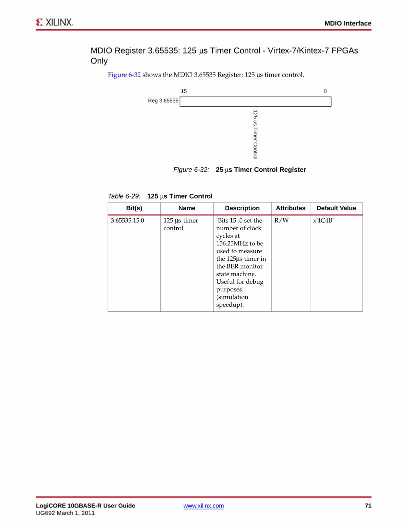
MDIO Interface
MDIO Register 3.65535: 125 μs Timer Control - Virtex-7/Kintex-7 FPGAs Only
Figure 6-32 shows the MDIO 3.65535 Register: 125 μs timer control.
Bit(s) Name Description Attributes Default Value
3.65535.15:0 125 μs timer control
Bits 15..0 set the number of clock cycles at 156.25MHz to be used to measure the 125μs timer in the BER monitor state machine. Useful for debug purposes (simulation speedup).
R/W x'4C4B'
X-Ref Target - Figure 6-32
Figure 6-32: 25 μs Timer Control Register
Table 6-29: 125 μs Timer Control
125 us Tim
er Control
15 0
Reg 3.65535
LogiCORE 10GBASE-R User Guide www.xilinx.com 71UG692 March 1, 2011
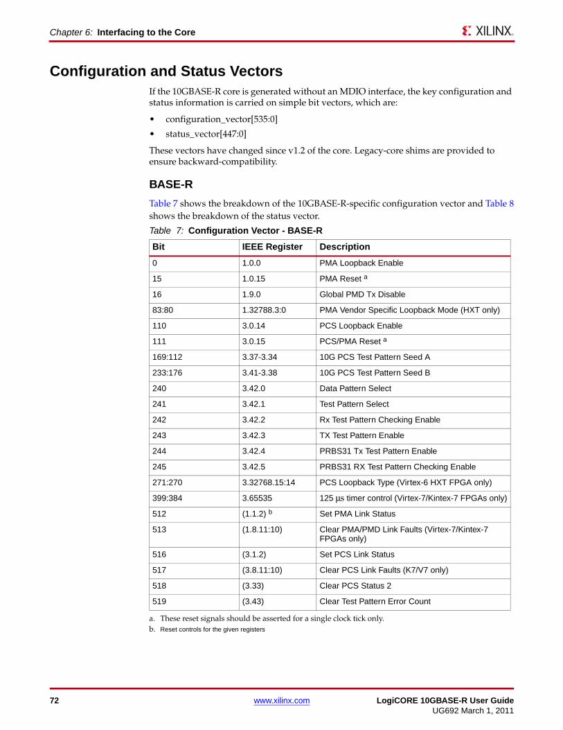
Chapter 6: Interfacing to the Core
Configuration and Status VectorsIf the 10GBASE-R core is generated without an MDIO interface, the key configuration and status information is carried on simple bit vectors, which are:
• configuration_vector[535:0]
• status_vector[447:0]
These vectors have changed since v1.2 of the core. Legacy-core shims are provided to ensure backward-compatibility.
BASE-R
Table 7 shows the breakdown of the 10GBASE-R-specific configuration vector and Table 8 shows the breakdown of the status vector.
0 1.0.0 PMA Loopback Enable
15 1.0.15 PMA Reset a
16 1.9.0 Global PMD Tx Disable
83:80 1.32788.3:0 PMA Vendor Specific Loopback Mode (HXT only)
110 3.0.14 PCS Loopback Enable
111 3.0.15 PCS/PMA Reset a
169:112 3.37-3.34 10G PCS Test Pattern Seed A
233:176 3.41-3.38 10G PCS Test Pattern Seed B
240 3.42.0 Data Pattern Select
241 3.42.1 Test Pattern Select
242 3.42.2 Rx Test Pattern Checking Enable
243 3.42.3 TX Test Pattern Enable
244 3.42.4 PRBS31 Tx Test Pattern Enable
245 3.42.5 PRBS31 RX Test Pattern Checking Enable
271:270 3.32768.15:14 PCS Loopback Type (Virtex-6 HXT FPGA only)
399:384 3.65535 125 μs timer control (Virtex-7/Kintex-7 FPGAs only)
512 (1.1.2) b Set PMA Link Status
513 (1.8.11:10) Clear PMA/PMD Link Faults (Virtex-7/Kintex-7 FPGAs only)
516 (3.1.2) Set PCS Link Status
517 (3.8.11:10) Clear PCS Link Faults (K7/V7 only)
518 (3.33) Clear PCS Status 2
519 (3.43) Clear Test Pattern Error Count
Table 7: Configuration Vector - BASE-R
Bit IEEE Register Description
a. These reset signals should be asserted for a single clock tick only.b. Reset controls for the given registers
72 www.xilinx.com LogiCORE 10GBASE-R User GuideUG692 March 1, 2011
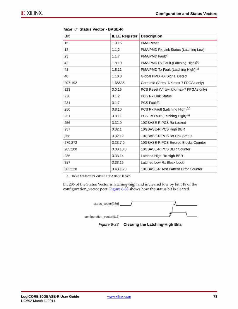
Configuration and Status Vectors
15 1.0.15 PMA Reset
18 1.1.2 PMA/PMD Rx Link Status (Latching Low)
23 1.1.7 PMA/PMD Faulta
42 1.8.10 PMA/PMD Rx Fault (Latching High) (a)
43 1.8.11 PMA/PMD Tx Fault (Latching High) (a)
48 1.10.0 Global PMD RX Signal Detect
207:192 1.65535 Core Info (Virtex-7/Kintex-7 FPGAs only)
223 3.0.15 PCS Reset (Virtex-7/Kintex-7 FPGAs only)
226 3.1.2 PCS Rx Link Status
231 3.1.7 PCS Fault (a)
250 3.8.10 PCS Rx Fault (Latching High) (a)
251 3.8.11 PCS Tx Fault (Latching High) (a)
256 3.32.0 10GBASE-R PCS Rx Locked
257 3.32.1 10GBASE-R PCS High BER
268 3.32.12 10GBASE-R PCS Rx Link Status
279:272 3.33.7:0 10GBASE-R PCS Errored Blocks Counter
285:280 3.33.13:8 10GBASE-R PCS BER Counter
286 3.33.14 Latched High Rx High BER
287 3.33.15 Latched Low Rx Block Lock
303:228 3.43.15:0 10GBASE-R Test Pattern Error Counter
Bit 286 of the Status Vector is latching-high and is cleared low by bit 518 of the configuration_vector port. Figure 6-33 shows how the status bit is cleared.
Table 8: Status Vector - BASE-R
Bit IEEE Register Description
a. This is tied to ’0’ for Virtex-6 FPGA BASE-R core
X-Ref Target - Figure 6-33
Figure 6-33: Clearing the Latching-High Bits
status_vector[286]
configuration_vector[518]
LogiCORE 10GBASE-R User Guide www.xilinx.com 73UG692 March 1, 2011
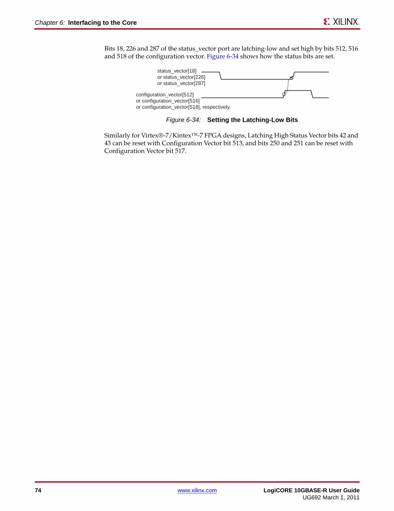
Chapter 6: Interfacing to the Core
Bits 18, 226 and 287 of the status_vector port are latching-low and set high by bits 512, 516 and 518 of the configuration vector. Figure 6-34 shows how the status bits are set.
Similarly for Virtex®-7/Kintex™-7 FPGA designs, Latching High Status Vector bits 42 and 43 can be reset with Configuration Vector bit 513, and bits 250 and 251 can be reset with Configuration Vector bit 517.
X-Ref Target - Figure 6-34
Figure 6-34: Setting the Latching-Low Bits
status_vector[18]or status_vector[226]or status_vector[287]
configuration_vector[512]or configuration_vector[516]or configuration_vector[518], respectively.
74 www.xilinx.com LogiCORE 10GBASE-R User GuideUG692 March 1, 2011
Chapter 7
Constraining the Core
This chapter describes how to constrain a design containing the 10GBASE-R core. This is illustrated by the UCF delivered with the core at generation time. See Chapter 10, Detailed Example Design, for a complete description of the CORE Generator™ software output files and for details of the HDL example design.
Caution! Not all constraints are relevant to specific implementations of the core; consult the UCF created with the core instance to see exactly which constraints are relevant.
Device, Package, and Speed Grade SelectionThis line selects the part to be used in the implementation run. Change this line so that it matches the part intended for the final application.
# Select the part to be used in the implementation runCONFIG PART = xc6vhx255t-ff1155-2;
Virtex-7/Kintex-7 FPGAsThe 10GBASE-R core can be implemented in many Virtex®-7/Kintex™-7 FPGA packages, as long as the package itself is a flip-chip package, and the GTX transceiver supports the 10.3125 Gb/s line-rate.
Virtex-6 FPGAsThe 10GBASE-R core can be implemented in most Virtex-6 HXT devices with any speed grade. Only the FF1154 packages are not supported (no bonded-out GTHs)
Clock Frequencies, Clock Management, and Placement
Virtex-7/Kintex-7 FPGAsThe 10GBASE-R core has one user clock domain:
• clk156 - 156.25 MHz derived from the txoutclk output of the Virtex-7/Kintex-7 FPGA GTX transceiver.
This section specifies the main clock frequencies for the design.
• rxclk156 - 156.25 MHz derived from the rxoutclk output of the Virtex-7/Kintex-7 FPGA GTX transceiver.
• txusrclk2 - 161.13 MHz derived from the txoutclk output of the Virtex-7/Kintex-7 FPGA GTX transceiver.
LogiCORE 10GBASE-R User Guide www.xilinx.com 75UG692 March 1, 2011
Chapter 7: Constraining the Core
• rxusrclk2 - 161.13 MHz derived from the rxoutclk output of the Virtex-7/Kintex-7 FPGA GTX transceiver.
General Clocking
• dclk - 78.125 MHz derived from the clk156 clock.
Virtex-6 FPGAsThe 10GBASE-R core has one user clock domain:
• The clk156 domain derived from the refclk input of the Virtex-6 FPGA GTH transceiver.
This section specifies the main clock frequencies for the design.
##################################################################### Clock frequencies and clock management #####################################################################NET "*txuserclkin" TNM_NET="clk156";TIMESPEC "TS_clk156" = PERIOD "clk156" 6400 ps;
NET "*rxuserclkin" TNM_NET="rxclk156";TIMESPEC "TS_rxclk156" = PERIOD "rxclk156" 6400 ps;
The clock frequency by default is set for 10-Gigabit Ethernet.General Clocking
NET "dclk" TNM_NET="dclk";TIMESPEC TS_dclk = PERIOD "dclk" 50 MHz;
This constraint defines the frequency of DCLK that is supplied to the Virtex-6 FPGA transceivers. The example design uses a nominal 50 MHz clock.
Other ConstraintsAmong other constraints you might find in the UCF, the following are required to control the routing between FFs on different clock domains.
# Elastic Buffer-related constraints ###################################################################NET "*elastic_buffer_i/asynch_fifo_i/rd_truegray<?>" MAXDELAY = 6.0 ns;NET "*elastic_buffer_i/can_insert_wra" TIG;NET "*elastic_buffer_i/asynch_fifo_i/wr_gray<?>" MAXDELAY = 6.0 ns;NET "*elastic_buffer_i/asynch_fifo_i/rd_lastgray<?>" MAXDELAY = 6.0 ns;
Transceiver Placement
Virtex-7/Kintex-7 FPGAsNo placement constraints have been introduced for the example design. Consult the 7 Series GTH Transceivers User Guide (UG476) for details.
Virtex-6 HXT FPGAsNo placement constraints have been introduced for the example design. Consult the Virtex-6 FPGA GTH Transceivers User Guide (UG371) for details.
76 www.xilinx.com LogiCORE 10GBASE-R User GuideUG692 March 1, 2011
MDIO
MDIO################################################################## MDIO-related constraints ##################################################################
INST "ten_gig_eth_pcs_pma_block/ten_gig_eth_pcs_pma_core/BU2/U0/*management_inst/mdc_reg1" IOB=TRUE;INST "ten_gig_eth_pcs_pma_block/ten_gig_eth_pcs_pma_core/BU2/U0/*management_inst/mdio_in_reg1" IOB=TRUE;INST "ten_gig_eth_pcs_pma_block/ten_gig_eth_pcs_pma_core/BU2/U0/*management_inst/mdio_interface_1/mdio_out" IOB=TRUE;INST "ten_gig_eth_pcs_pma_block/ten_gig_eth_pcs_pma_core/BU2/U0/*management_inst/mdio_interface_1/mdio_tri" IOB=TRUE;
These constraints set the correct attributes for the registers at the edge of the MDIO block. The TIMESPEC constrains the MDIO interface to 2.5 MHz. If you wish to overclock the MDIO interface, you must alter this constraint.
LogiCORE 10GBASE-R User Guide www.xilinx.com 77UG692 March 1, 2011

Chapter 7: Constraining the Core
78 www.xilinx.com LogiCORE 10GBASE-R User GuideUG692 March 1, 2011
Chapter 8
Design Considerations
This chapter describes considerations that can apply in particular design cases.
Virtex-7/Kintex-7 FPGAs
ClockingThe clocking schemes in this section are illustrative only and can require customization for a specific application.
Reference Clock
For Virtex®-7/Kintex™-7 FPGA GTX transceivers, the reference clock must be running at 161.1328125 MHz. (This number is abbreviated to 161.13 MHz henceforth).
Transceiver Placement
A single IBUFDS_GTE2 block is used to feed the reference clocks for all GTXE2_CHANNEL transceivers, via a GTXE2_COMMON block.
For details about Virtex-7/Kintex-7 FPGA transceiver clock distribution, see the section on Clocking in the 7 Series GTH Transceivers User Guide (UG476).
Internal Client-Side Interface
The clocking scheme for the internal client interface is shown in Figure 8-1.
The GTXE2_CHANNEL primitives require a 161.13 MHz reference clock, as well as 161.13 MHz and 322.16 MHz TX and RX user clocks. The latter must be created from the 322.26 MHz TXOUTCLK and RXOUTCLK outputs from that block.
The 156.25 MHz user-logic clock rxclk156 must be created from the 161.13 MHz RXUSRCLK2 GTXE2 clock, in order to track small variations in receive data rates.
The 156.25 MHz user-logic clock clk156 must be created from the 161.13 MHz TXUSRCLK2 GTXE2 clock in order to keep the user logic and GTXE2 synchronous.
A dedicated management/configuration clock, dclk, is used by the user logic and the GTXE2 and must be created from the clk156, at half the rate; that is: 78.125 MHz.
LogiCORE 10GBASE-R User Guide www.xilinx.com 79UG692 March 1, 2011
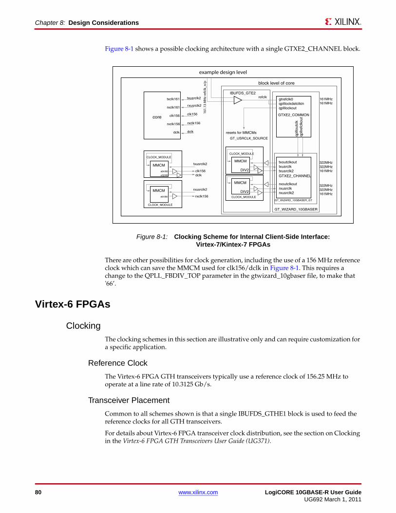
Chapter 8: Design Considerations
Figure 8-1 shows a possible clocking architecture with a single GTXE2_CHANNEL block.
There are other possibilities for clock generation, including the use of a 156 MHz reference clock which can save the MMCM used for clk156/dclk in Figure 8-1. This requires a change to the QPLL_FBDIV_TOP parameter in the gtwizard_10gbaser file, to make that '66’.
Virtex-6 FPGAs
ClockingThe clocking schemes in this section are illustrative only and can require customization for a specific application.
Reference Clock
The Virtex-6 FPGA GTH transceivers typically use a reference clock of 156.25 MHz to operate at a line rate of 10.3125 Gb/s.
Transceiver Placement
Common to all schemes shown is that a single IBUFDS_GTHE1 block is used to feed the reference clocks for all GTH transceivers.
For details about Virtex-6 FPGA transceiver clock distribution, see the section on Clocking in the Virtex-6 FPGA GTH Transceivers User Guide (UG371).
X-Ref Target - Figure 8-1
Figure 8-1: Clocking Scheme for Internal Client-Side Interface: Virtex-7/Kintex-7 FPGAs
80 www.xilinx.com LogiCORE 10GBASE-R User GuideUG692 March 1, 2011
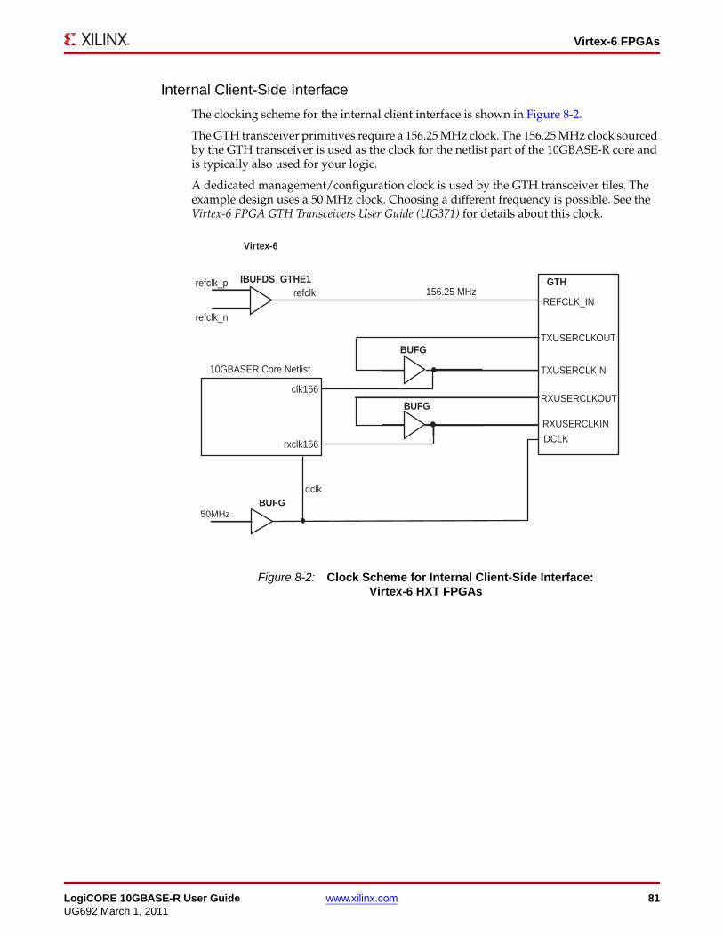
Virtex-6 FPGAs
Internal Client-Side Interface
The clocking scheme for the internal client interface is shown in Figure 8-2.
The GTH transceiver primitives require a 156.25 MHz clock. The 156.25 MHz clock sourced by the GTH transceiver is used as the clock for the netlist part of the 10GBASE-R core and is typically also used for your logic.
A dedicated management/configuration clock is used by the GTH transceiver tiles. The example design uses a 50 MHz clock. Choosing a different frequency is possible. See the Virtex-6 FPGA GTH Transceivers User Guide (UG371) for details about this clock.X-Ref Target - Figure 8-2
Figure 8-2: Clock Scheme for Internal Client-Side Interface: Virtex-6 HXT FPGAs
TXUSERCLKIN
REFCLK_IN
TXUSERCLKOUT
RXUSERCLKOUT
GTH
DCLK
clk156
Virtex-6
IBUFDS_GTHE1refclk_prefclk
refclk_n
BUFG
dclk
50MHz
BUFG
156.25 MHz
10GBASER Core Netlist
RXUSERCLKIN
rxclk156
BUFG
LogiCORE 10GBASE-R User Guide www.xilinx.com 81UG692 March 1, 2011
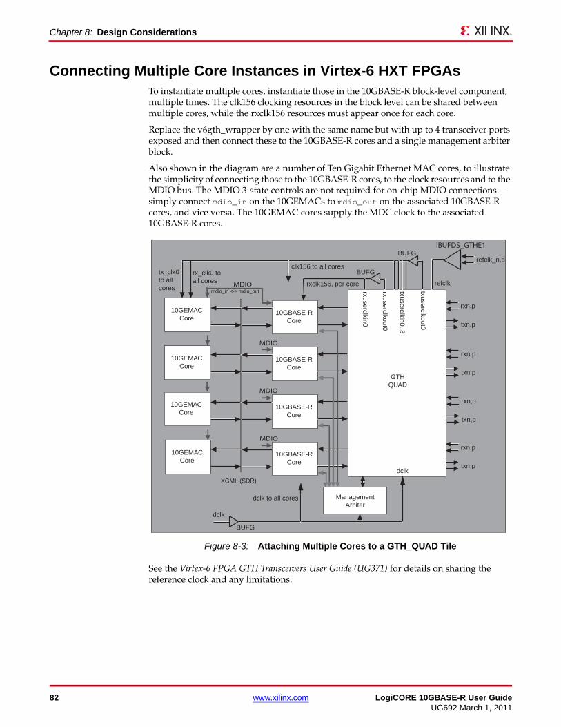
Chapter 8: Design Considerations
Connecting Multiple Core Instances in Virtex-6 HXT FPGAsTo instantiate multiple cores, instantiate those in the 10GBASE-R block-level component, multiple times. The clk156 clocking resources in the block level can be shared between multiple cores, while the rxclk156 resources must appear once for each core.
Replace the v6gth_wrapper by one with the same name but with up to 4 transceiver ports exposed and then connect these to the 10GBASE-R cores and a single management arbiter block.
Also shown in the diagram are a number of Ten Gigabit Ethernet MAC cores, to illustrate the simplicity of connecting those to the 10GBASE-R cores, to the clock resources and to the MDIO bus. The MDIO 3-state controls are not required for on-chip MDIO connections – simply connect mdio_in on the 10GEMACs to mdio_out on the associated 10GBASE-R cores, and vice versa. The 10GEMAC cores supply the MDC clock to the associated 10GBASE-R cores.
See the Virtex-6 FPGA GTH Transceivers User Guide (UG371) for details on sharing the reference clock and any limitations.
X-Ref Target - Figure 8-3
Figure 8-3: Attaching Multiple Cores to a GTH_QUAD Tile
XGMII (SDR)
GTHQUAD
rxn,p
txn,p
rxn,p
txn,p
rxn,p
txn,p
rxn,p
txn,p
MDIO
ManagementArbiter
10GBASE-RCore
10GBASE-RCore
10GBASE-RCore
10GBASE-RCore
refclk_n,p
IBUFDS_GTHE1
refclk
txuserclkout0
txuserclkin0..3
clk156 to all cores
dclk
BUFG
BUFG
rxuserclkout0
rxuserclkin0
rxclk156, per core
BUFG
dclk to all cores
dclk
10GEMACCore
tx_clk0to allcores
rx_clk0 toall cores
10GEMACCore
10GEMACCore
10GEMACCore
mdio_in <-> mdio_outMDIO
MDIO
MDIO
82 www.xilinx.com LogiCORE 10GBASE-R User GuideUG692 March 1, 2011
Using the DRP in Virtex-6 HXT FPGAs
Using the DRP in Virtex-6 HXT FPGAsThe core, combined with the management arbiter block, accesses the GTH transceiver internal registers through the MGMT interface to the GTH transceiver. To do this, the DRP interface to the GTH transceiver must be disabled. This happens automatically when the core wishes to access those registers.
Access to the DRP is still available to the user, by setting the drp_req pin on the management arbiter, and waiting for the drp_gnt signal to be asserted before starting any DRP access. This allows any MGMT interface accesses to complete before switching over to the DRP interface and disabling the MGMT interface. The DRP interface is used exclusively until drp_req is set low again.
Reset CircuitsAll register resets within the 10GBASE-R core netlist are synchronized to the relevant clock port.
Receiver Termination: Virtex-7/Kintex-7 FPGAsThe receiver termination must be set correctly. See the 7 Series FPGA GTH Transceivers User Guide.
Receiver Termination: Virtex-6 FPGAsThe receiver termination must be set correctly. See the Virtex-6 FPGA GTH Transceivers User Guide (UG371).
LogiCORE 10GBASE-R User Guide www.xilinx.com 83UG692 March 1, 2011
Chapter 8: Design Considerations
84 www.xilinx.com LogiCORE 10GBASE-R User GuideUG692 March 1, 2011
Chapter 9
Implementing the Core
This chapter describes how to simulate and implement your design containing the 10GBASE-R core.
Pre-implementation SimulationA unit delay gate-level model of the 10GBASE-R core netlist is provided as a CORE Generator™ software output file. This can be used for simulation of the block in the design phase of a project.
Using the Simulation ModelFor information about setting up your simulator to use the pre-implemented model, consult the Xilinx® Synthesis and Verification Design Guide, included in your Xilinx software installation.
The unit delay gate-level model of the 10GBASE-R core can be found in the CORE Generator software project directory. Details of the CORE Generator software outputs can be found in Chapter 10, Detailed Example Design.
VHDL
component_name.vhd
Verilog
component_name.v
LogiCORE 10GBASE-R User Guide www.xilinx.com 85UG692 March 1, 2011
Chapter 9: Implementing the Core
Synthesis
XST: VHDLIn the CORE Generator software project directory, there is a component_name.vho file that is a component and instantiation template for the core. Use this to help instantiate the 10GBASE-R core into your VHDL source.
After your entire design is complete, create:
• An XST project file top_level_module_name.prj listing all your source code files
• An XST script file top_level_module_name.scr containing your required synthesis options
To synthesize the design, run:
$ xst -ifn top_level_module_name.scr
See the XST User Guide for details on creating project and synthesis script files and running the xst program.
XST: VerilogIn the CORE Generator software project directory, there is a module declaration for the 10GBASE-R core at:
<project_directory>/<component_name>/implement/component_name_mod.v
Use this module to help instance the 10GBASE-R core into your Verilog source.
After your entire design is complete, create:
• An XST project file top_level_module_name.prj listing all your source code files. Make sure you include:
%XILINX%/verilog/src/iSE/unisim_comp.v
and
<project_directory>/<component_name>/implement/component_name_mod.v
as the first two files in the project list.
• An XST script file top_level_module_name.scr containing your required synthesis options.
To synthesize the design, run:
$ xst -ifn top_level_module_name.scr
See the XST User Guide for details about creating project and synthesis script files, and running the xst program.
86 www.xilinx.com LogiCORE 10GBASE-R User GuideUG692 March 1, 2011
Implementation
Implementation
Generating the Xilinx NetlistTo generate the Xilinx netlist, the ngdbuild tool is used to translate and merge the individual design netlists into a single design database, the NGD file. Also merged at this stage is the User Constraints File (UCF) for the design. An example of the ngdbuild command is:
$ ngdbuild top_level_module_name_example_design
Mapping the DesignTo map the logic gates of your design netlist into the CLBs and IOBs of the FPGA, run the map command. The map command writes out a physical design to an NCD file. An example of the map command is:
$ map -o mapped.ncd top_level_module_name_example_design
Placing and Routing the DesignTo place and route your design logic components (mapped physical logic cells) contained within an NCD file in accordance with the layout and timing requirements specified in the PCF file, the par command must be executed. The par command outputs the placed and routed physical design to an NCD file. An example of the par command is:
$ par mapped.ncd routed mapped.pcf
Static Timing AnalysisTo evaluate timing closure on a design and create a Timing Report file (TWR) derived from static timing analysis of the Physical Design file (NCD), the trce command must be executed. The analysis is typically based on constraints included in the optional PCF file. An example of the trce command is:
$ trce -e 10 routed -o routed mapped.pcf
Generating a BitstreamTo create the configuration bitstream (BIT) file based on the contents of a physical implementation file (NCD), the bitgen command must be executed. The BIT file defines the behavior of the programmed FPGA. An example of the bitgen command is:
$ bitgen routed.ncd routed.bit mapped.pcf
LogiCORE 10GBASE-R User Guide www.xilinx.com 87UG692 March 1, 2011
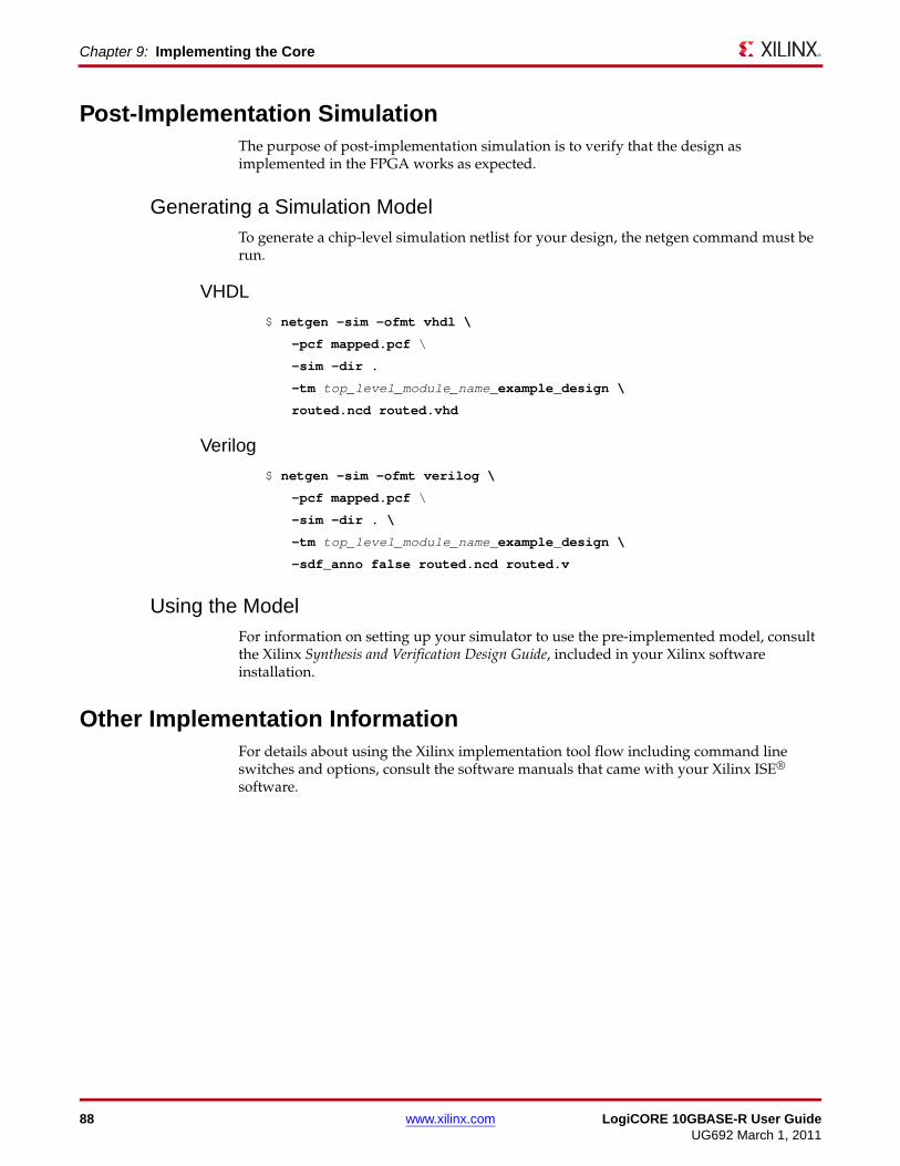
Chapter 9: Implementing the Core
Post-Implementation SimulationThe purpose of post-implementation simulation is to verify that the design as implemented in the FPGA works as expected.
Generating a Simulation ModelTo generate a chip-level simulation netlist for your design, the netgen command must be run.
VHDL
$ netgen -sim -ofmt vhdl \
-pcf mapped.pcf \
-sim -dir .
-tm top_level_module_name_example_design \
routed.ncd routed.vhd
Verilog
$ netgen -sim -ofmt verilog \
-pcf mapped.pcf \
-sim -dir . \
-tm top_level_module_name_example_design \
-sdf_anno false routed.ncd routed.v
Using the ModelFor information on setting up your simulator to use the pre-implemented model, consult the Xilinx Synthesis and Verification Design Guide, included in your Xilinx software installation.
Other Implementation InformationFor details about using the Xilinx implementation tool flow including command line switches and options, consult the software manuals that came with your Xilinx ISE® software.
88 www.xilinx.com LogiCORE 10GBASE-R User GuideUG692 March 1, 2011
Chapter 10
Detailed Example Design
This chapter provides detailed information about the example design, including a description of the files and the directory structure generated by the Xilinx® CORE Generator™ software, the purpose and contents of the provided scripts, the contents of the example HDL wrappers, and the operation of the demonstration test bench.top directory link - white text invisible
<project directory>topdirectory
Top-level project directory; name is user-defined.
<project directory>/<component name> Core release notes file
<component_name>/doc Product documentation
<component_name>/example_designVerilog and VHDL design files
<component_name>/implementImplementation script files
implement/results Results directory, created after implementation scripts are run, and contains implement script results
<component_name>/simulationSimulation scripts
simulation/functionalFunctional simulation files
simulation/timingTiming simulation files
LogiCORE 10GBASE-R User Guide www.xilinx.com 89UG692 March 1, 2011
Chapter 10: Detailed Example Design
Directory and File ContentsThe core directories and their associated files are defined in the following sections.
<project directory> The project directory contains all the CORE Generator software project files.
Name Description
A binary Xilinx implementation netlist. Describes how the core is to be implemented. Used as an input to the Xilinx implementation tools.
VHDL or Verilog structural simulation model. File used to support functional simulation of a core.
As an output file, the XCO file is a log file which records the settings used to generate a particular core. An XCO file is generated by the CORE Generator software for each core that it creates in the current project directory. An XCO file can also be used as an input to the CORE Generator software.
List of files delivered with the core
A VHDL or Verilog template for the core. This can be copied into your design.
Back to Top
<project directory>/<component name>The <component name> directory contains the release notes file provided with the core, which can include last-minute changes and updates.
Name Description
Core release notes file
Back to Top
Table 10-1: Project Directory
<project_dir>
<component_name>.ngc
<component_name>.v[hd]
<component_name>.xco
<component_name>_flist.txt
<component_name>.{veo|vho}
Table 10-2: Component Name Directory
<project_dir>/<component_name>
ten_gig_eth_pcs_pma_readme.txt
90 www.xilinx.com LogiCORE 10GBASE-R User GuideUG692 March 1, 2011
Directory and File Contents
<component_name>/docThe doc directory contains the PDF documentation provided with the core.
Name Description
10GBASE-R Data Sheet
10GBASE-R User Guide
Back to Top
<component_name>/example_designThe example design directory contains the example design files provided with the core.
Name Description
Block entity containing the 10GBASE-R core and transceiver wrappers
Top-level entity for the example design containing the block level design and clocking circuitry
User constraints file for the core and example design
Wrapper file for the 10GBASE-R core
Arbiter for multiple cores accessing GTH_QUAD
Used to reproduce the original core configuration vector bit numbering
Used to reproduce the original core status vector bit numbering
Back to Top
Table 10-3: Doc Directory
<project_dir>/<component_name>/doc
ten_gig_eth_pcs_pma_ds739.pdf
ten_gig_eth_pcs_pma_ug692.pdf
Table 10-4: Example Design Directory
<project_dir>/<component_name>/example_design
<component_name>_block.v[hd]
<component_name>_example_design.v[hd]
<component_name>_example_design.ucf
<component_name>_mod.v
management_arbiter.v[hd] (Virtex-6 FPGAs only)
legacy_config_shim.v[hd] (Virtex-6 FPGAs only)
legacy_status_shim.v[hd] (Virtex-6 FPGAs only)
LogiCORE 10GBASE-R User Guide www.xilinx.com 91UG692 March 1, 2011
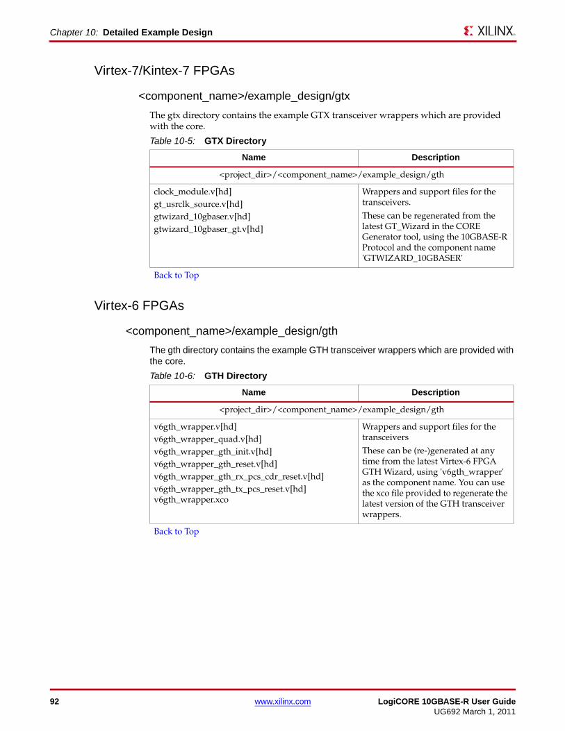
Chapter 10: Detailed Example Design
Virtex-7/Kintex-7 FPGAs
<component_name>/example_design/gtx
The gtx directory contains the example GTX transceiver wrappers which are provided with the core.
Name Description
Wrappers and support files for the transceivers.
These can be regenerated from the latest GT_Wizard in the CORE Generator tool, using the 10GBASE-R Protocol and the component name 'GTWIZARD_10GBASER'
Back to Top
Virtex-6 FPGAs
<component_name>/example_design/gth
The gth directory contains the example GTH transceiver wrappers which are provided with the core.
Name Description
Wrappers and support files for the transceivers
These can be (re-)generated at any time from the latest Virtex-6 FPGA GTH Wizard, using 'v6gth_wrapper' as the component name. You can use the xco file provided to regenerate the latest version of the GTH transceiver wrappers.
Back to Top
Table 10-5: GTX Directory
<project_dir>/<component_name>/example_design/gth
clock_module.v[hd]gt_usrclk_source.v[hd]gtwizard_10gbaser.v[hd]gtwizard_10gbaser_gt.v[hd]
Table 10-6: GTH Directory
<project_dir>/<component_name>/example_design/gth
v6gth_wrapper.v[hd]v6gth_wrapper_quad.v[hd] v6gth_wrapper_gth_init.v[hd]v6gth_wrapper_gth_reset.v[hd]v6gth_wrapper_gth_rx_pcs_cdr_reset.v[hd]v6gth_wrapper_gth_tx_pcs_reset.v[hd] v6gth_wrapper.xco
92 www.xilinx.com LogiCORE 10GBASE-R User GuideUG692 March 1, 2011
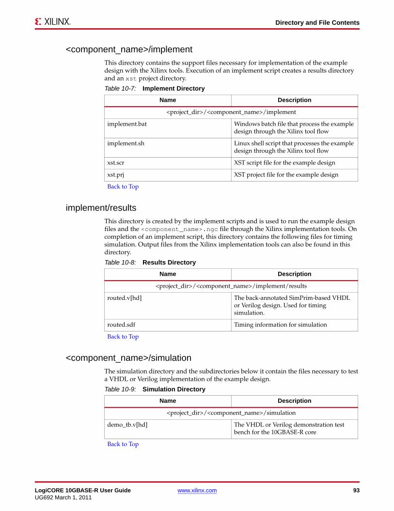
Directory and File Contents
<component_name>/implementThis directory contains the support files necessary for implementation of the example design with the Xilinx tools. Execution of an implement script creates a results directory and an xst project directory.
Name Description
<project_dir>/<component_name>/implement
Windows batch file that process the example design through the Xilinx tool flow
Linux shell script that processes the example design through the Xilinx tool flow
XST script file for the example design
XST project file for the example design
Back to Top
implement/resultsThis directory is created by the implement scripts and is used to run the example design files and the <component_name>.ngc file through the Xilinx implementation tools. On completion of an implement script, this directory contains the following files for timing simulation. Output files from the Xilinx implementation tools can also be found in this directory.
Name Description
<project_dir>/<component_name>/implement/results
The back-annotated SimPrim-based VHDL or Verilog design. Used for timing simulation.
Timing information for simulation
Back to Top
<component_name>/simulationThe simulation directory and the subdirectories below it contain the files necessary to test a VHDL or Verilog implementation of the example design.
Name Description
<project_dir>/<component_name>/simulation
The VHDL or Verilog demonstration test bench for the 10GBASE-R core
Back to Top
Table 10-7: Implement Directory
implement.bat
implement.sh
xst.scr
xst.prj
Table 10-8: Results Directory
routed.v[hd]
routed.sdf
Table 10-9: Simulation Directory
demo_tb.v[hd]
LogiCORE 10GBASE-R User Guide www.xilinx.com 93UG692 March 1, 2011
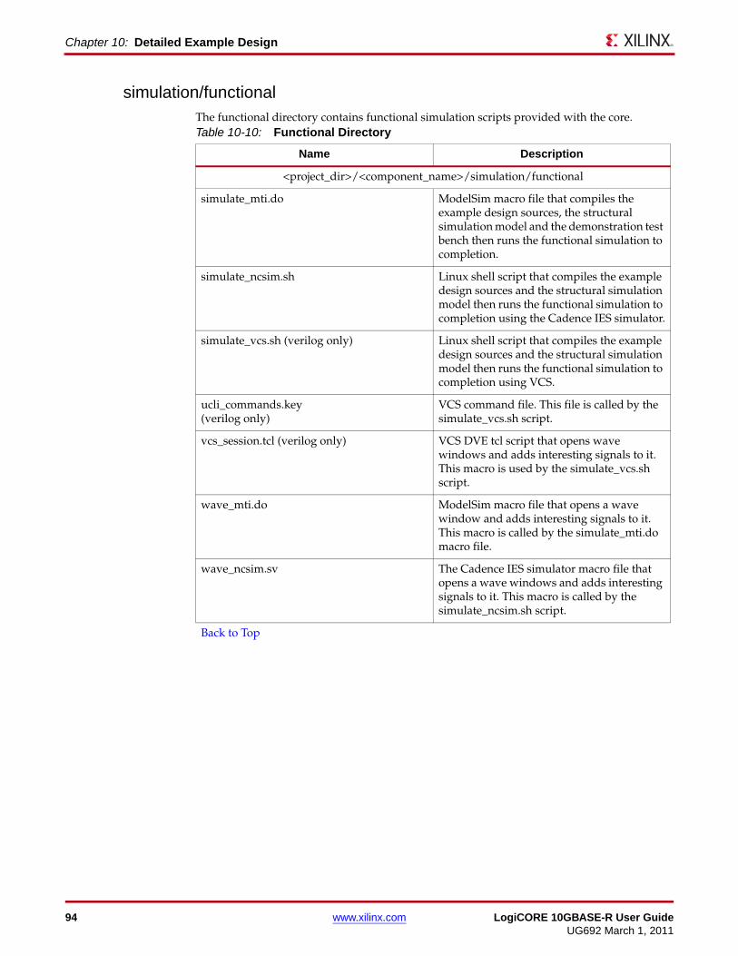
Chapter 10: Detailed Example Design
simulation/functionalThe functional directory contains functional simulation scripts provided with the core.
Name Description
<project_dir>/<component_name>/simulation/functional
ModelSim macro file that compiles the example design sources, the structural simulation model and the demonstration test bench then runs the functional simulation to completion.
Linux shell script that compiles the example design sources and the structural simulation model then runs the functional simulation to completion using the Cadence IES simulator.
Linux shell script that compiles the example design sources and the structural simulation model then runs the functional simulation to completion using VCS.
VCS command file. This file is called by the simulate_vcs.sh script.
VCS DVE tcl script that opens wave windows and adds interesting signals to it. This macro is used by the simulate_vcs.sh script.
ModelSim macro file that opens a wave window and adds interesting signals to it. This macro is called by the simulate_mti.do macro file.
The Cadence IES simulator macro file that opens a wave windows and adds interesting signals to it. This macro is called by the simulate_ncsim.sh script.
Back to Top
Table 10-10: Functional Directory
simulate_mti.do
simulate_ncsim.sh
simulate_vcs.sh (verilog only)
ucli_commands.key (verilog only)
vcs_session.tcl (verilog only)
wave_mti.do
wave_ncsim.sv
94 www.xilinx.com LogiCORE 10GBASE-R User GuideUG692 March 1, 2011
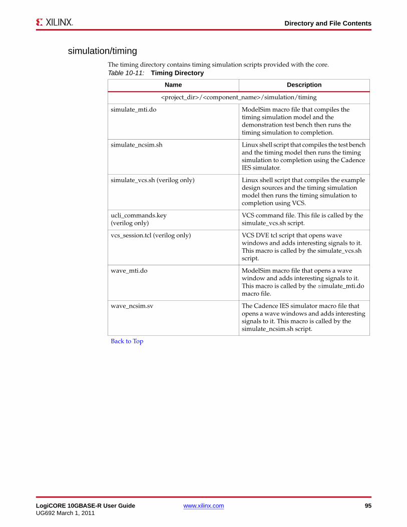
Directory and File Contents
simulation/timingThe timing directory contains timing simulation scripts provided with the core.
Name Description
<project_dir>/<component_name>/simulation/timing
ModelSim macro file that compiles the timing simulation model and the demonstration test bench then runs the timing simulation to completion.
Linux shell script that compiles the test bench and the timing model then runs the timing simulation to completion using the Cadence IES simulator.
Linux shell script that compiles the example design sources and the timing simulation model then runs the timing simulation to completion using VCS.
VCS command file. This file is called by the simulate_vcs.sh script.
VCS DVE tcl script that opens wave windows and adds interesting signals to it. This macro is called by the simulate_vcs.sh script.
ModelSim macro file that opens a wave window and adds interesting signals to it. This macro is called by the simulate_mti.do macro file.
The Cadence IES simulator macro file that opens a wave windows and adds interesting signals to it. This macro is called by the simulate_ncsim.sh script.
Back to Top
Table 10-11: Timing Directory
simulate_mti.do
simulate_ncsim.sh
simulate_vcs.sh (verilog only)
ucli_commands.key (verilog only)
vcs_session.tcl (verilog only)
wave_mti.do
wave_ncsim.sv
LogiCORE 10GBASE-R User Guide www.xilinx.com 95UG692 March 1, 2011
Chapter 10: Detailed Example Design
Implementation and Test Scripts
Implementation ScriptThe implementation script is either a shell script or batch file that processes the example design through the Xilinx tool flow. The script is located at:
Linux
<project_dir>/<component_name>/implement/implement.sh
Windows
<project_dir>/<component_name>/implement/implement.bat
The implement script performs these steps:
• The example HDL wrapper is synthesized using XST.
• ngdbuild is run to consolidate the core netlist and the wrapper netlist into the NGD file containing the entire design.
• The design is mapped to the target technology.
• The design is place-and-routed on the target device.
• Static timing analysis is performed on the routed design using trce.
• A bitstream is generated.
• netgen runs on the routed design to generate VHDL and Verilog netlists and timing information in the form of SDF files.
The implement script is only generated when Full license is available for the 10GBASE-R core.
Setting up for SimulationThe Xilinx UniSim library must be mapped into the simulator. If the library is not set up for your environment, go to Answer Record 15338 for assistance compiling Xilinx simulation models and for setting up the simulator environment.
All Virtex® FPGA designs require a Verilog LRM-IEEE 1364-2005 encryption-compliant simulator. For a Verilog LRM-IEEE 1364-2005 encryption-compliant simulator, the following simulators are supported.
• Mentor Graphics ModelSim version 6.6d
• Cadence Incisive Enterprise Simulator v10.2
• Synopsys VCS and VCS MX 2010.06
96 www.xilinx.com LogiCORE 10GBASE-R User GuideUG692 March 1, 2011
Implementation and Test Scripts
Simulation ScriptsSimulation macro files are provided for ModelSim and shell scripts are provided for the Cadence IES simulator and Synopsys VCS simulator. The scripts automate the simulation of the test bench and can be found in the following location:
Functional
<project_dir>/<component_name>/simulation/functional/simulate_mti.do
<project_dir>/<component_name>/simulation/functional/simulate_ncsim.sh
<project_dir>/<component_name>/simulation/functional/simulate_vcs.sh
Timing
<project_dir>/<component_name>/simulation/timing/simulate_mti.do
<project_dir>/<component_name>/simulation/timing/simulate_ncsim.sh
<project_dir>/<component_name>/simulation/timing/simulate_vcs.sh
The scripts perform these tasks:
• Compiles the gate level netlist
• Compiles the demonstration test bench
• Starts a simulation of the test bench (with timing information if a Full-system Evaluation license or Full license is in use)
• Opens a Wave window and adds some interesting signals (wave_mti.do/wave_ncsim.sv/vcs_session.tcl)
• Runs the simulation to completion
Libraries
The user must ensure that any required simulation support files are created in the simulation/functional and/or simulation/timing directories. These can include library-directory mappings such as those contained in the modelsim.ini file for ModelSim and cds.lib and hdl.var files for IES.
LogiCORE 10GBASE-R User Guide www.xilinx.com 97UG692 March 1, 2011
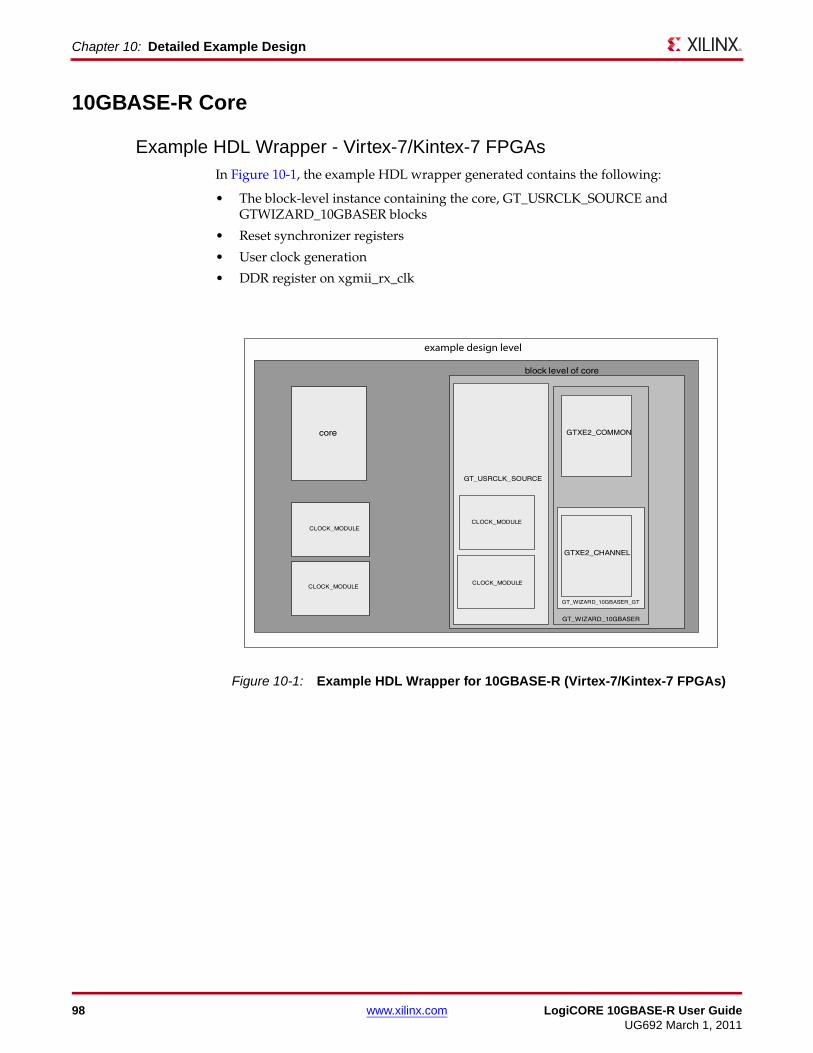
Chapter 10: Detailed Example Design
10GBASE-R Core
Example HDL Wrapper - Virtex-7/Kintex-7 FPGAsIn Figure 10-1, the example HDL wrapper generated contains the following:
• The block-level instance containing the core, GT_USRCLK_SOURCE and GTWIZARD_10GBASER blocks
• Reset synchronizer registers
• User clock generation
• DDR register on xgmii_rx_clk
X-Ref Target - Figure 10-1
Figure 10-1: Example HDL Wrapper for 10GBASE-R (Virtex-7/Kintex-7 FPGAs)
98 www.xilinx.com LogiCORE 10GBASE-R User GuideUG692 March 1, 2011
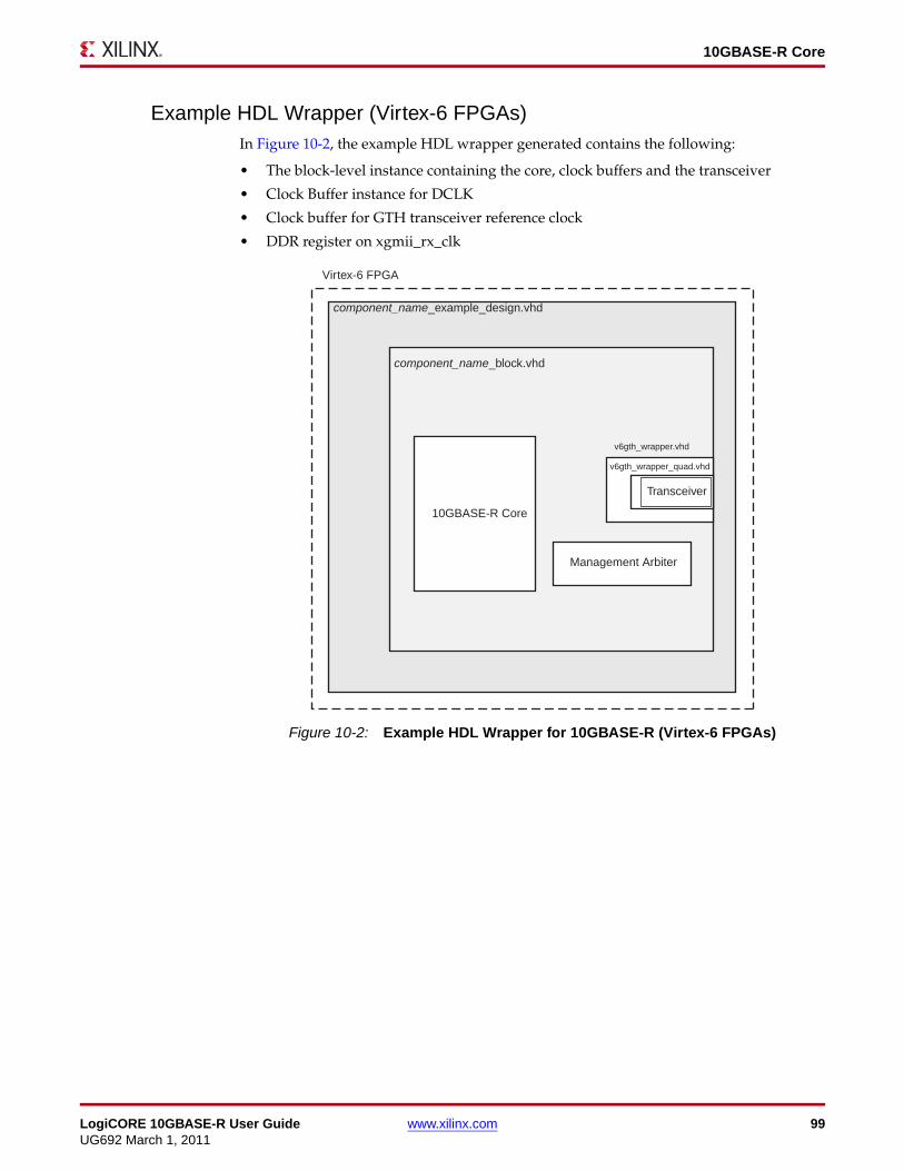
10GBASE-R Core
Example HDL Wrapper (Virtex-6 FPGAs)In Figure 10-2, the example HDL wrapper generated contains the following:
• The block-level instance containing the core, clock buffers and the transceiver
• Clock Buffer instance for DCLK
• Clock buffer for GTH transceiver reference clock
• DDR register on xgmii_rx_clkX-Ref Target - Figure 10-2
Figure 10-2: Example HDL Wrapper for 10GBASE-R (Virtex-6 FPGAs)
10GBASE-R Core
Virtex-6 FPGA
component_name_example_design.vhd
component_name_block.vhd
Transceiver
v6gth_wrapper_quad.vhd
v6gth_wrapper.vhd
Management Arbiter
LogiCORE 10GBASE-R User Guide www.xilinx.com 99UG692 March 1, 2011
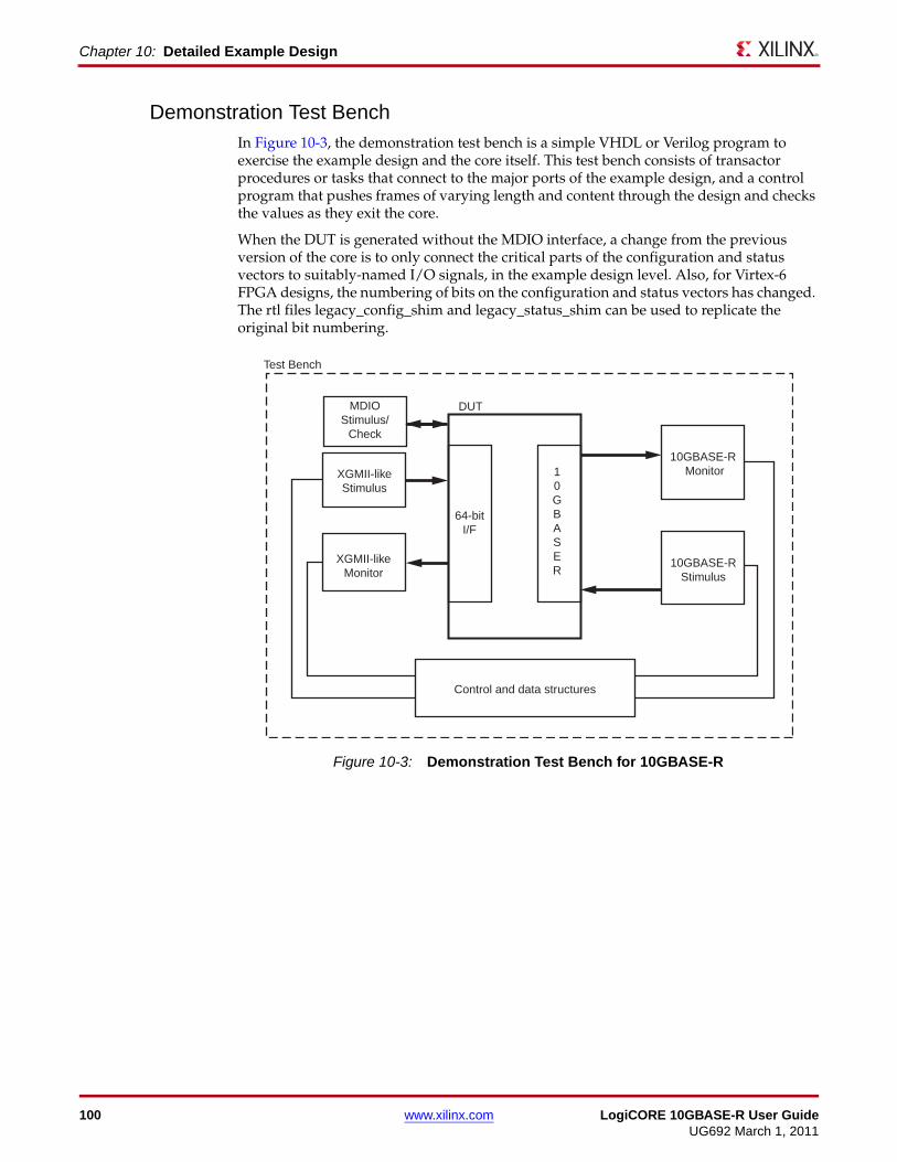
Chapter 10: Detailed Example Design
Demonstration Test BenchIn Figure 10-3, the demonstration test bench is a simple VHDL or Verilog program to exercise the example design and the core itself. This test bench consists of transactor procedures or tasks that connect to the major ports of the example design, and a control program that pushes frames of varying length and content through the design and checks the values as they exit the core.
When the DUT is generated without the MDIO interface, a change from the previous version of the core is to only connect the critical parts of the configuration and status vectors to suitably-named I/O signals, in the example design level. Also, for Virtex-6 FPGA designs, the numbering of bits on the configuration and status vectors has changed. The rtl files legacy_config_shim and legacy_status_shim can be used to replicate the original bit numbering.X-Ref Target - Figure 10-3
Figure 10-3: Demonstration Test Bench for 10GBASE-R
10GBASE-R Monitor
10GBASE-RStimulus
XGMII-likeStimulus
XGMII-likeMonitor
64-bitI/F
10GBASER
DUT
Test Bench
Control and data structures
MDIOStimulus/
Check
100 www.xilinx.com LogiCORE 10GBASE-R User GuideUG692 March 1, 2011
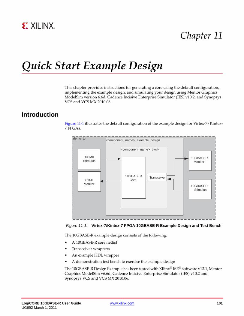
Chapter 11
Quick Start Example Design
This chapter provides instructions for generating a core using the default configuration, implementing the example design, and simulating your design using Mentor Graphics ModelSim version 6.6d, Cadence Incisive Enterprise Simulator (IES) v10.2, and Synopsys VCS and VCS MX 2010.06.
IntroductionFigure 11-1 illustrates the default configuration of the example design for Virtex-7/Kintex-7 FPGAs.
The 10GBASE-R example design consists of the following:
• A 10GBASE-R core netlist
• Transceiver wrappers
• An example HDL wrapper
• A demonstration test bench to exercise the example design
The 10GBASE-R Design Example has been tested with Xilinx® ISE® software v13.1, Mentor Graphics ModelSim v6.6d, Cadence Incisive Enterprise Simulator (IES) v10.2 and Synopsys VCS and VCS MX 2010.06.
X-Ref Target - Figure 11-1
Figure 11-1: Virtex-7/Kintex-7 FPGA 10GBASE-R Example Design and Test Bench
<component_name>_example_design
<component_name>_block
demo_tb
XGMIIStimulus
XGMIIMonitor
Transceiver10GBASER Core
10GBASER Monitor
10GBASER Stimulus
LogiCORE 10GBASE-R User Guide www.xilinx.com 101UG692 March 1, 2011
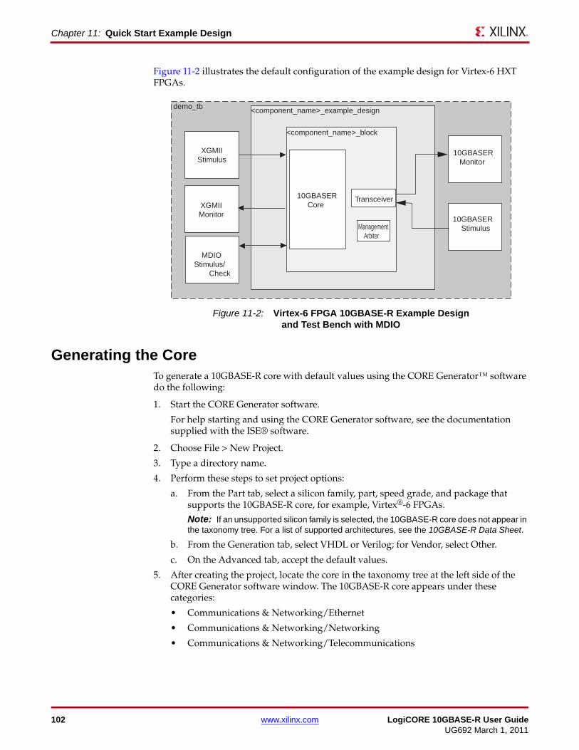
Chapter 11: Quick Start Example Design
Figure 11-2 illustrates the default configuration of the example design for Virtex-6 HXT FPGAs.
Generating the CoreTo generate a 10GBASE-R core with default values using the CORE Generator™ software do the following:
1. Start the CORE Generator software.
For help starting and using the CORE Generator software, see the documentation supplied with the ISE® software.
2. Choose File > New Project.
3. Type a directory name.
4. Perform these steps to set project options:
a. From the Part tab, select a silicon family, part, speed grade, and package that supports the 10GBASE-R core, for example, Virtex®-6 FPGAs.
Note: If an unsupported silicon family is selected, the 10GBASE-R core does not appear in the taxonomy tree. For a list of supported architectures, see the 10GBASE-R Data Sheet.
b. From the Generation tab, select VHDL or Verilog; for Vendor, select Other.
c. On the Advanced tab, accept the default values.
5. After creating the project, locate the core in the taxonomy tree at the left side of the CORE Generator software window. The 10GBASE-R core appears under these categories:
• Communications & Networking/Ethernet
• Communications & Networking/Networking
• Communications & Networking/Telecommunications
X-Ref Target - Figure 11-2
Figure 11-2: Virtex-6 FPGA 10GBASE-R Example Design and Test Bench with MDIO
<component_name>_example_design
<component_name>_block
demo_tb
XGMIIStimulus
XGMIIMonitor
Transceiver10GBASER Core
10GBASER Monitor
10GBASER Stimulus
MDIOStimulus/
Check
Management Arbiter
102 www.xilinx.com LogiCORE 10GBASE-R User GuideUG692 March 1, 2011
Implementing the 10GBASE-R Example Design
6. Double-click the core to open it. A message can appear warning you about the limitations of the Simulation Only license, and then the 10GBASE-R customization screen appears.
7. In the Component Name field, enter a name for the core instance.
8. Accept the remaining default options and click Generate to generate the core.
The core and its supporting files, including the example design, are generated in the project directory. For a detailed description of the directory structure and files, see Detailed Example Design in Chapter 10.
Implementing the 10GBASE-R Example DesignAfter the core is successfully generated, the netlist and example design HDL wrapper can be processed through the Xilinx implementation tools. The generated outputs include several scripts to assist in processing.
Open a command prompt or shell in your project directory and enter the following commands:
Linux% cd <component_name>/implement
% source ./implement.sh
Windows> cd <component_name>\implement
> implement.bat
The implement command accomplishes the following:
• Starts a script to synthesize the example design HDL wrapper
• Builds, maps, and place-and-routes the example design (Full license only)
• Creates gate-level netlist HDL files with associated timing information (SDF files)
The created files are placed in the results directory which is created by the implement script at run time.
Simulating the 10GBASE-R Example DesignThe example design provided with the 10GBASE-R core provides a complete environment which allows you to simulate the core and view the outputs. Scripts are provided for pre- and post-implementation simulation. The simulation model is either in VHDL or Verilog depending on the CORE Generator software Design Entry project option.
Setting up for SimulationTo run the gate-level simulation you must have the Xilinx Simulation Libraries compiled for your system. See the Compiling Xilinx Simulation Libraries (COMPXLIB) in the Xilinx ISE Synthesis and Verification Design Guide, and the Xilinx ISE Software Manuals and Help. You can download these documents from: www.xilinx.com/support/software_manuals.htm.
LogiCORE 10GBASE-R User Guide www.xilinx.com 103UG692 March 1, 2011
Chapter 11: Quick Start Example Design
The Xilinx simulation libraries must be mapped into the simulator. If the libraries are not set for your environment, go to Answer Record 15338 on www.xilinx.com/support for assistance compiling Xilinx simulation models and setting up the simulator environment.
All Virtex device designs require a Verilog LRM-IEEE 1364-2005 encryption-compliant simulator. For a Verilog LRM-IEEE 1364-2005 encryption-compliant simulator, these simulators are supported.
• Mentor Graphics ModelSim version 6.6d
• Cadence Incisive Enterprise Simulator v10.2
• Synopsys VCS and VCS MX 2010.06
Pre-Implementation SimulationTo run a functional simulation of the example design:
1. Open a command prompt or shell in your project directory and set the current directory to
<component_name>/simulation/functional
2. Launch the simulation script:
ModelSim: vsim -do simulate_mti.do
Cadence sim: ./simulate_ncsim.sh
vcs: ./simulate_vcs.sh
The simulation script compiles the functional model and the demonstration test bench, adds some relevant signals to a wave window, and then runs the simulation to completion. You can then inspect the simulation transcript and waveform to observe the operation of the core.
Post-Implementation SimulationTo run a timing simulation of the example design:
1. Open a command prompt or shell in your project directory, then set the current directory to:
<component_name>/simulation/timing
2. Launch the simulation script:
ModelSim: vsim -do simulate_mti.do
Cadence sim: ./simulate_ncsim.sh
vcs: ./simulate_vcs.sh
The simulation script compiles the gate-level model and the demonstration test bench, adds some relevant signals to a wave window, and then runs the simulation to completion. You can then inspect the simulation transcript and waveform to observe the operation of the core.
Additional InformationFor details about the example design, including guidelines for modifying the design and extending the test bench, see Chapter 10, Detailed Example Design.
104 www.xilinx.com LogiCORE 10GBASE-R User GuideUG692 March 1, 2011
Appendix A
Verification and Interoperability
The 10GBASE-R core has been verified using simulation.
A highly parameterizable transaction-based simulation test suite has been used to verify the core. Tests included:
• Register access over MDIO or Configuration/Status vectors
• Loss and re-gain of synchronization
• Loss and re-gain of alignment
• Frame transmission
• Frame reception
• Clock compensation
• Recovery from error conditions
LogiCORE 10GBASE-R User Guide www.xilinx.com 105UG692 March 1, 2011
Appendix A: Verification and Interoperability
106 www.xilinx.com LogiCORE 10GBASE-R User GuideUG692 March 1, 2011
Appendix B
Core Latency
These measurements are for the core only; they do not include the latency through the transceiver. The latency through the transceiver can be obtained from the relevant user guide.
Virtex-7/Kintex-7 FPGAs
Transmit Path LatencyAs measured from the input port xgmii_txd[63:0] of the transmitter side XGMII (until that data appears on gt_txd[63:0] on the transceiver interface), the latency through the core for the internal XGMII interface configuration in the transmit direction is 9 periods of clk156.
Receive Path LatencyMeasured from the input into the core on gt_rxd[63:0] until the data appears on xgmii_rxd[63:0] of the receiver side XGMII interface, the latency through the core in the receive direction is nominally equal to 26 cycles of rxclk156, including +/- 4 cycles in the elastic buffer. The latency depends on sync bit alignment position and data positioning within the transceiver 4-byte interface.
GTX Transceiver LatencyLatency through the GTX Transceiver in the transmit direction is nominally 5 cycles of clk156.
Latency through the GTX Transceiver in the receive direction is nominally 3 cycles of rxclk156 plus a number of bit-times between zero and 65, in the RX Alignment Buffer.
See the 7 Series GTX Transceivers User Guide (UG476) for information on the GTX transceiver latency.
Virtex-6 HXT FPGAs
Transmit Path LatencyAs measured from the input port xgmii_txd[63:0] of the transmitter side XGMII (until that data appears on gt_txd[63:0] on the transceiver interface), the latency through the core for the internal XGMII interface configuration in the transmit direction is 2 clk periods of the core input clk156.
LogiCORE 10GBASE-R User Guide www.xilinx.com 107UG692 March 1, 2011
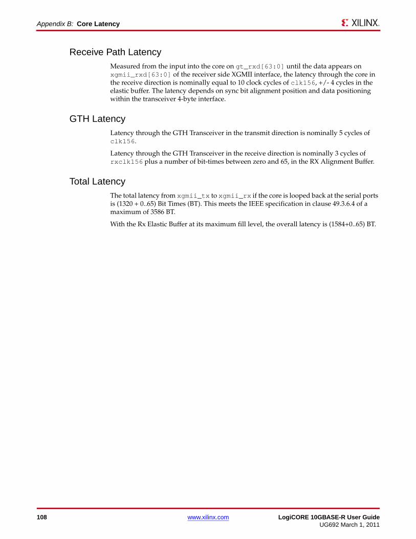
Appendix B: Core Latency
Receive Path LatencyMeasured from the input into the core on gt_rxd[63:0] until the data appears on xgmii_rxd[63:0] of the receiver side XGMII interface, the latency through the core in the receive direction is nominally equal to 10 clock cycles of clk156, +/- 4 cycles in the elastic buffer. The latency depends on sync bit alignment position and data positioning within the transceiver 4-byte interface.
GTH LatencyLatency through the GTH Transceiver in the transmit direction is nominally 5 cycles of clk156.
Latency through the GTH Transceiver in the receive direction is nominally 3 cycles of rxclk156 plus a number of bit-times between zero and 65, in the RX Alignment Buffer.
Total LatencyThe total latency from xgmii_tx to xgmii_rx if the core is looped back at the serial ports is (1320 + 0..65) Bit Times (BT). This meets the IEEE specification in clause 49.3.6.4 of a maximum of 3586 BT.
With the Rx Elastic Buffer at its maximum fill level, the overall latency is (1584+0..65) BT.
108 www.xilinx.com LogiCORE 10GBASE-R User GuideUG692 March 1, 2011