Embed Size (px)
Citation preview
Device XMC1300Marking/Step EES-AB, ES-AB, ABPackage PG-TSSOP-16/38, PG-VQFN-24/40
Rel. 1.3, 2015-06
XMC1300, EES-AB, ES-AB, AB 1/28 Rel. 1.3, 2015-06Subject to Agreement on the Use of Product Information
Errata Sheet
OverviewThis “Errata Sheet” describes product deviations with respect to the userdocumentation listed below.
Make sure that you always use the latest documentation for this device listed incategory “Documents” at http://www.infineon.com/xmc1000.
Notes1. The errata described in this sheet apply to all temperature and frequency
versions and to all memory size and configuration variants of affected devices, unless explicitly noted otherwise.
2. Devices marked with EES or ES are engineering samples which may not be completely tested in all functional and electrical characteristics, therefore they must be used for evaluation only. The specific test conditions for EES and ES are documented in a separate “Status Sheet”.
Table 1 Current User DocumentationDocument Version DateXMC1300 Reference Manual AB-step V1.2 Nov 2014XMC1300 Data Sheet AB-step V1.6 Apr 2015
Errata Sheet
XMC1300, EES-AB, ES-AB, AB 2/28 Rel. 1.3, 2015-06Subject to Agreement on the Use of Product Information
Conventions used in this DocumentEach erratum is identified by Module_Marker.TypeNumber:• Module: Subsystem, peripheral, or function affected by the erratum.• Marker: Used only by Infineon internal.• Type: type of deviation
– (none): Functional Deviation– P: Parametric Deviation– H: Application Hint– D: Documentation Update
• Number: Ascending sequential number. As this sequence is used over several derivatives, including already solved deviations, gaps inside this enumeration can occur.
Errata SheetHistory List / Change Summary
XMC1300, EES-AB, ES-AB, AB 3/28 Rel. 1.3, 2015-06Subject to Agreement on the Use of Product Information
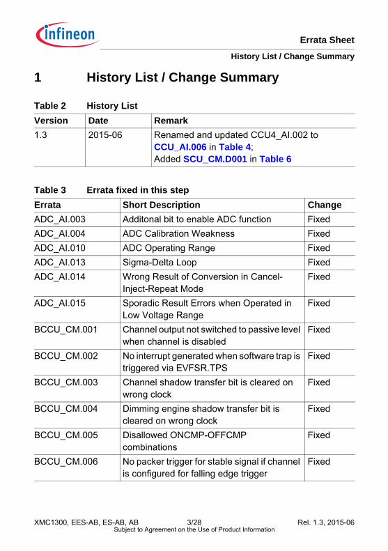
1 History List / Change Summary
Table 2 History ListVersion Date Remark1.3 2015-06 Renamed and updated CCU4_AI.002 to
CCU_AI.006 in Table 4;Added SCU_CM.D001 in Table 6
Table 3 Errata fixed in this stepErrata Short Description ChangeADC_AI.003 Additonal bit to enable ADC function FixedADC_AI.004 ADC Calibration Weakness FixedADC_AI.010 ADC Operating Range FixedADC_AI.013 Sigma-Delta Loop FixedADC_AI.014 Wrong Result of Conversion in Cancel-
Inject-Repeat ModeFixed
ADC_AI.015 Sporadic Result Errors when Operated in Low Voltage Range
Fixed
BCCU_CM.001 Channel output not switched to passive level when channel is disabled
Fixed
BCCU_CM.002 No interrupt generated when software trap is triggered via EVFSR.TPS
Fixed
BCCU_CM.003 Channel shadow transfer bit is cleared on wrong clock
Fixed
BCCU_CM.004 Dimming engine shadow transfer bit is cleared on wrong clock
Fixed
BCCU_CM.005 Disallowed ONCMP-OFFCMP combinations
Fixed
BCCU_CM.006 No packer trigger for stable signal if channel is configured for falling edge trigger
Fixed
Errata SheetHistory List / Change Summary
XMC1300, EES-AB, ES-AB, AB 4/28 Rel. 1.3, 2015-06Subject to Agreement on the Use of Product Information
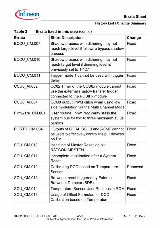
BCCU_CM.007 Shadow process with dithering may not reach target level if follows a bypass shadow process
Fixed
BCCU_CM.010 Shadow process with dithering may not reach target level if dimming level is previously set to 1-127
Fixed
BCCU_CM.011 Trigger mode 1 cannot be used with trigger delay
Fixed
CCU8_AI.002 CC82 Timer of the CCU8x module cannot use the external shadow transfer trigger connected to the POSIFx module
Fixed
CCU8_AI.004 CCU8 output PWM glitch when using low side modulation via the Multi Channel Mode
Fixed
Firmware_CM.001 User routine _NvmProgVerify stalls the system bus for two to three maximum 10 µs periods
Fixed
PORTS_CM.004 Outputs of CCU4, BCCU and ACMP cannot be used to effectively control the pull devices on Pin
Fixed
SCU_CM.010 Handling of Master Reset via bit RSTCON.MRSTEN
Fixed
SCU_CM.011 Incomplete Initialisation after a System Reset
Fixed
SCU_CM.012 Calibrating DCO based on Temperature Sensor
Removed
SCU_CM.013 Brownout reset triggered by External Brownout Detector (BDE)
Fixed
SCU_CM.014 Temperature Sensor User Routines in ROM FixedSCU_CM.016 Usage of Offset Formulae for DCO
Calibration based on TemperatureFixed
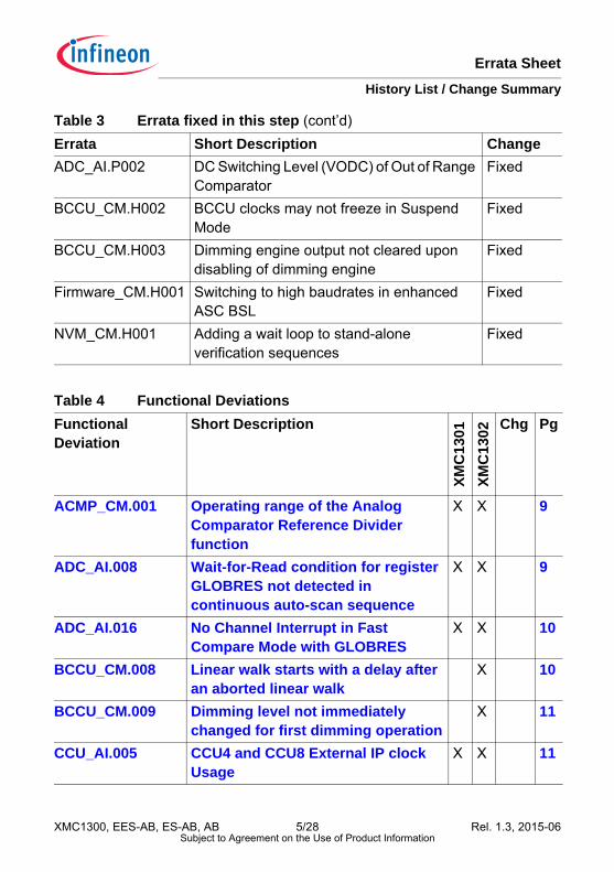
Table 3 Errata fixed in this step (cont’d)Errata Short Description Change
Errata SheetHistory List / Change Summary
XMC1300, EES-AB, ES-AB, AB 5/28 Rel. 1.3, 2015-06Subject to Agreement on the Use of Product Information
ADC_AI.P002 DC Switching Level (VODC) of Out of Range Comparator
Fixed
BCCU_CM.H002 BCCU clocks may not freeze in Suspend Mode
Fixed
BCCU_CM.H003 Dimming engine output not cleared upon disabling of dimming engine
Fixed
Firmware_CM.H001 Switching to high baudrates in enhanced ASC BSL
Fixed
NVM_CM.H001 Adding a wait loop to stand-alone verification sequences
Fixed
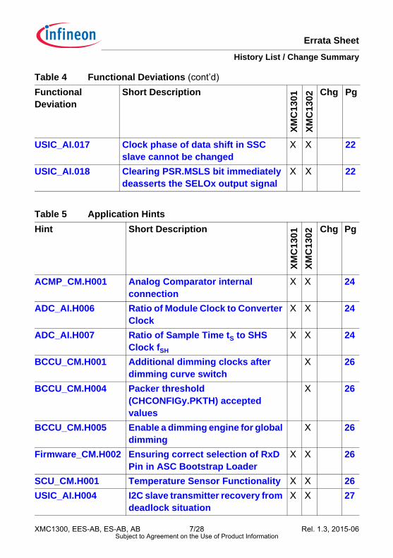
Table 4 Functional DeviationsFunctional Deviation
Short Description
XM
C13
01
XM
C13
02 Chg Pg
ACMP_CM.001 Operating range of the Analog Comparator Reference Divider function
X X 9
ADC_AI.008 Wait-for-Read condition for register GLOBRES not detected in continuous auto-scan sequence
X X 9
ADC_AI.016 No Channel Interrupt in Fast Compare Mode with GLOBRES
X X 10
BCCU_CM.008 Linear walk starts with a delay after an aborted linear walk
X 10
BCCU_CM.009 Dimming level not immediately changed for first dimming operation
X 11
CCU_AI.005 CCU4 and CCU8 External IP clock Usage
X X 11
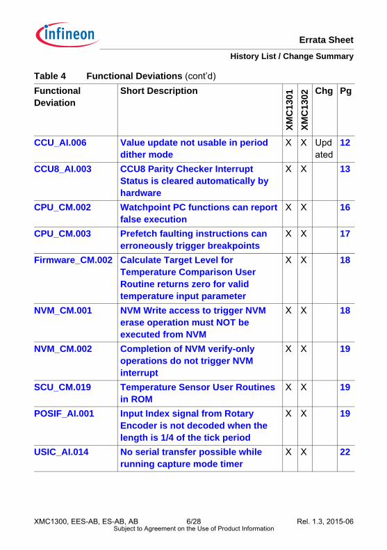
Table 3 Errata fixed in this step (cont’d)Errata Short Description Change
Errata SheetHistory List / Change Summary
XMC1300, EES-AB, ES-AB, AB 6/28 Rel. 1.3, 2015-06Subject to Agreement on the Use of Product Information
CCU_AI.006 Value update not usable in period dither mode
X X Updated
12
CCU8_AI.003 CCU8 Parity Checker Interrupt Status is cleared automatically by hardware
X X 13
CPU_CM.002 Watchpoint PC functions can report false execution
X X 16
CPU_CM.003 Prefetch faulting instructions can erroneously trigger breakpoints
X X 17
Firmware_CM.002 Calculate Target Level for Temperature Comparison User Routine returns zero for valid temperature input parameter
X X 18
NVM_CM.001 NVM Write access to trigger NVM erase operation must NOT be executed from NVM
X X 18
NVM_CM.002 Completion of NVM verify-only operations do not trigger NVM interrupt
X X 19
SCU_CM.019 Temperature Sensor User Routines in ROM
X X 19
POSIF_AI.001 Input Index signal from Rotary Encoder is not decoded when the length is 1/4 of the tick period
X X 19
USIC_AI.014 No serial transfer possible while running capture mode timer
X X 22
Table 4 Functional Deviations (cont’d)Functional Deviation
Short Description
XM
C13
01
XM
C13
02 Chg Pg
Errata SheetHistory List / Change Summary
XMC1300, EES-AB, ES-AB, AB 7/28 Rel. 1.3, 2015-06Subject to Agreement on the Use of Product Information
USIC_AI.017 Clock phase of data shift in SSC slave cannot be changed
X X 22
USIC_AI.018 Clearing PSR.MSLS bit immediately deasserts the SELOx output signal
X X 22
Table 5 Application HintsHint Short Description
XM
C13
01
XM
C13
02 Chg Pg
ACMP_CM.H001 Analog Comparator internal connection
X X 24
ADC_AI.H006 Ratio of Module Clock to Converter Clock
X X 24
ADC_AI.H007 Ratio of Sample Time tS to SHS Clock fSH
X X 24
BCCU_CM.H001 Additional dimming clocks after dimming curve switch
X 26
BCCU_CM.H004 Packer threshold (CHCONFIGy.PKTH) accepted values
X 26
BCCU_CM.H005 Enable a dimming engine for global dimming
X 26
Firmware_CM.H002 Ensuring correct selection of RxD Pin in ASC Bootstrap Loader
X X 26
SCU_CM.H001 Temperature Sensor Functionality X X 26USIC_AI.H004 I2C slave transmitter recovery from
deadlock situationX X 27
Table 4 Functional Deviations (cont’d)Functional Deviation
Short Description
XM
C13
01
XM
C13
02 Chg Pg
Errata SheetHistory List / Change Summary
XMC1300, EES-AB, ES-AB, AB 8/28 Rel. 1.3, 2015-06Subject to Agreement on the Use of Product Information
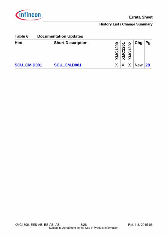
Table 6 Documentation UpdatesHint Short Description
XM
C12
00
XM
C12
01
XM
C12
02 Chg Pg
SCU_CM.D001 SCU_CM.D001 X X X New 28
Errata SheetFunctional Deviations
XMC1300, EES-AB, ES-AB, AB 9/28 Rel. 1.3, 2015-06Subject to Agreement on the Use of Product Information
2 Functional DeviationsThe errata in this section describe deviations from the documented functionalbehavior.
ACMP_CM.001 Operating range of the Analog Comparator Reference Di-vider function
The Analog Comparator Reference Divider function is not available when VDDPis below 3 V. To use this function, VDDP must be between 3 V to 5.5 V.
WorkaroundNone
ADC_AI.008 Wait-for-Read condition for register GLOBRES not detectedin continuous auto-scan sequence
In the following scenario:• A continuous auto-scan is performed over several ADC groups and
channels by the Background Scan Source, using the global result register (GLOBRES) as result target (GxCHCTRy.RESTBS=1B), and
• The Wait-for-Read mode for GLOBRES is enabled (GLOBCR.WFR=1B), each conversion of the auto-scan sequence has to wait for its start until theresult of the previous conversion has been read out of GLOBRES. When the last channel of the auto-scan is converted and its result written toGLOBRES, the auto-scan re-starts with the highest channel number of thehighest ADC group number. But the start of this channel does not wait until theresult of the lowest channel of the previous sequence has been read fromregister GLOBRES, i.e. the result of the lowest channel may be lost.
WorkaroundIf either the last or the first channel in the auto-scan sequence does not write itsresult into GLOBRES, but instead into its group result register (selected via bit
Errata SheetFunctional Deviations
XMC1300, EES-AB, ES-AB, AB 10/28 Rel. 1.3, 2015-06Subject to Agreement on the Use of Product Information
GxCHCTRy.RESTBS=0B), then the Wait-for-Read feature for GLOBRES workscorrectly for all other channels of the auto-scan sequence. For this purpose, the auto-scan sequence may be extended by a “dummy”conversion of group x/ channel y, where the Wait-for-Read mode must not beselected (GxRCRy.WFR=0B) if the result of this “dummy” conversion is notread.
ADC_AI.016 No Channel Interrupt in Fast Compare Mode with GLOBRES
In fast compare mode, the compare value is taken from bitfield RESULT of theselected result register and the result of the comparison is stored in therespective bit FCR. A channel event can be generated when the input becomes higher or lower thanthe compare value. In case the global result register GLOBRES is selected, the comparison isexecuted correctly, the target bit is stored correctly, source events and resultevents are generated, but a channel event is not generated.
WorkaroundIf channel events are required, choose a local result register GxRESy for theoperation of the fast compare channel.
BCCU_CM.008 Linear walk starts with a delay after an aborted linear walk
If a linear walk is previously aborted, the subsequent linear walk starts with adelay. The maximum delay is one linear clock.
WorkaroundNone.
Errata SheetFunctional Deviations
XMC1300, EES-AB, ES-AB, AB 11/28 Rel. 1.3, 2015-06Subject to Agreement on the Use of Product Information
BCCU_CM.009 Dimming level not immediately changed for first dimmingoperation
For the first dimming operation, the dimming level is not immediatelyincremented or decremented upon a shadow bit (DES) assertion.
WorkaroundNone.
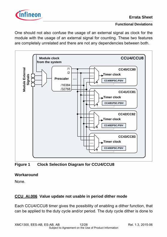
CCU_AI.005 CCU4 and CCU8 External IP clock Usage
Each CCU4/CCU8 module offers the possibility of selecting an external signalto be used as the master clock for every timer inside the module Figure 1.External signal in this context is understood as a signal connected to othermodule/IP or connected to the device ports.The user has the possibility after selecting what is the clock for the module(external signal or the clock provided by the system), to also select if this clockneeds to be divided. The division ratios start from 1 (no frequency division) upto 32768 (where the selected timer uses a frequency of the selected clockdivided by 32768).This division is selected by the PSIV field inside of the CC4yPSC/CC8yPSCregister. Notice that each Timer Slice (CC4y/CC8y) have a specific PSIV field,which means that each timer can operate in a different frequency.Currently is only possible to use an external signal as Timer Clock when adivision ratio of 2 or higher is selected. When no division is selected (divided by1), the external signal cannot be used.The user must program the PSIV field of each Timer Slice with a value differentfrom 0000B - minimum division value is /2.This is only applicable if the Module Clock provided by the system (the normaldefault configuration and use case scenario) is not being used. In the case thatthe normal clock configured and programmed at system level is being used,there is not any type of constraints.
Errata SheetFunctional Deviations
XMC1300, EES-AB, ES-AB, AB 12/28 Rel. 1.3, 2015-06Subject to Agreement on the Use of Product Information
One should not also confuse the usage of an external signal as clock for themodule with the usage of an external signal for counting. These two featuresare completely unrelated and there are not any dependencies between both.
Figure 1 Clock Selection Diagram for CCU4/CCU8
WorkaroundNone.
CCU_AI.006 Value update not usable in period dither mode
Each CCU4/CCU8 timer gives the possibility of enabling a dither function, thatcan be applied to the duty cycle and/or period. The duty cycle dither is done to
CCU4/CCU8
CC40/CC80
... ... Timer clock
CC41/CC81
... Timer clock
CC42/CC82
... Timer clock
CC43/CC83
... Timer clock
Module clock from the system
Mod
ule
Exte
rnal
Si
gnal
s
Prescaler
/1/2
/16384/32768
CC4/80PSC.PSIV
CC4/81PSC.PSIV
CC4/82PSC.PSIV
CC4/83PSC.PSIV
Errata SheetFunctional Deviations
XMC1300, EES-AB, ES-AB, AB 13/28 Rel. 1.3, 2015-06Subject to Agreement on the Use of Product Information
increase the resolution of the PWM duty cycle over time. The period dither isdone to increase the resolution of the PWM switching frequency over time. Each of the dither configurations is set via the DITHE field: • DITHE = 00B - dither disabled• DITHE = 01B - dither applied to the duty-cycle (compare value)• DITHE = 10B - dither applied to the period (period value)• DITHE = 11B - dither applied to the duty-cycle and period (compare an
period value)Whenever the dither function is applied to the period (DITHE = 10B or DITHE =11B ) and an update of the period value is done via a shadow transfer, the timercan enter a stuck-at condition (stuck at 0).
ImplicationPeriod value update via shadow transfer cannot be used if dither function isapplied to the period (DITHE programmed to 10B or 11B ).
WorkaroundNone
CCU8_AI.003 CCU8 Parity Checker Interrupt Status is cleared automati-cally by hardware
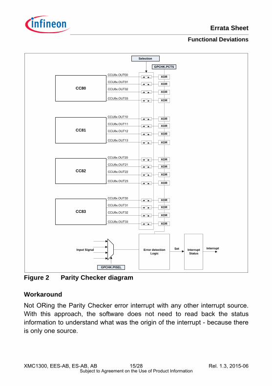
Each CCU8 Module Timer has an associated interrupt status register. ThisStatus register, CC8yINTS, keeps the information about which interrupt sourcetriggered an interrupt. The status of this interrupt source can only be cleared bysoftware. This is an advantage because the user can configure multipleinterrupt sources to the same interrupt line and in each triggered interruptroutine, it reads back the status register to know which was the origin of theinterrupt.Each CCU8 module also contains a function called Parity Checker. This ParityChecker function, crosschecks the output of a XOR structure versus an inputsignal, as seen in Figure 1.
Errata SheetFunctional Deviations
XMC1300, EES-AB, ES-AB, AB 14/28 Rel. 1.3, 2015-06Subject to Agreement on the Use of Product Information
When using the parity checker function, the associated status bitfield, is clearedautomatically by hardware in the next PWM cycle whenever an error is notpresent.This means that if in the previous PWM cycle an error was detected and oneinterrupt was triggered, the software needs to read back the status registerbefore the end of the immediately next PWM cycle. This is indeed only necessary if multiple interrupt sources are ORed together inthe same interrupt line. If this is not the case and the parity checker error sourceis the only one associated with an interrupt line, then there is no need to readback the status information. This is due to the fact, that only one action can betriggered in the software routine, the one linked with the parity checker error.
Errata SheetFunctional Deviations
XMC1300, EES-AB, ES-AB, AB 15/28 Rel. 1.3, 2015-06Subject to Agreement on the Use of Product Information
Figure 2 Parity Checker diagram
WorkaroundNot ORing the Parity Checker error interrupt with any other interrupt source.With this approach, the software does not need to read back the statusinformation to understand what was the origin of the interrupt - because thereis only one source.
CCU8x.OUT00
CCU8x.OUT01
CCU8x.OUT02CC80
CCU8x.OUT03
CCU8x.OUT10
CCU8x.OUT11
CCU8x.OUT12CC81
CCU8x.OUT13
CCU8x.OUT20
CCU8x.OUT21
CCU8x.OUT22CC82
CCU8x.OUT23
CCU8x.OUT30
CCU8x.OUT31
CCU8x.OUT32CC83
CCU8x.OUT33
Input Signal
GPCHK.PISEL
GPCHK.PCTS
Set
Selection
XOR
XOR
XOR
XOR
XOR
XOR
XOR
XOR
XOR
XOR
XOR
XOR
XOR
XOR
XOR
XOR
Error detection Logic
Interrupt Status
Interrupt
Errata SheetFunctional Deviations
XMC1300, EES-AB, ES-AB, AB 16/28 Rel. 1.3, 2015-06Subject to Agreement on the Use of Product Information
CPU_CM.002 Watchpoint PC functions can report false execution
In the presence of interrupts including those generated by the SVC instruction,it is possible for both the data watchpoint unit's PC match facility and PCsample-register to operate as though the instruction immediately following theinterrupted or SVC instruction had been executed.
ConditionsEither:1. Halting debug is enabled via C_DEBUGEN = 12. Watchpoints are enabled via DWTENA = 13. A watchpoint is configured for PC sampling DWT_FUNCTION = 0x44. The same watchpoint is configured to match a `target instruction`5. And either:
a) The `target instruction` is interrupted before execution, orb) The `target instruction` is preceded by a taken SVC instruction
6. The DWT will unexpectedly match the `target instruction`7. The processor will unexpectedly enter debug state once inside the
exception handlerOr:1. The debugger performs a read access to the DWT_PCSR2. A `non-committed instruction` is preceded by a taken SVC instruction3. The DWT_PCSR value unexpectedly matches the `non-committed
instruction`
ImplicationsIf halting debug is enabled and PC match watchpoints are being used, thenspurious entry into halted debug state may occur under the listed conditions.If the DWT_PCSR is being used for coarse grain profiling, then it is possible thatthe results can include hits for the address of an instruction immediately afteran SVC instruction, even if said instruction is never executed.
WorkaroundThis errata does not impact normal execution of the processor.
Errata SheetFunctional Deviations
XMC1300, EES-AB, ES-AB, AB 17/28 Rel. 1.3, 2015-06Subject to Agreement on the Use of Product Information
A debug agent may choose to handle the infrequent false positive Debug stateentry and erroneous PCSR values as spurious events.
CPU_CM.003 Prefetch faulting instructions can erroneously triggerbreakpoints
External prefetch aborts on instruction fetches on which a BPU breakpoint hasbeen configured, will cause entry to Debug state. This is prohibited by revisionC of the ARMv6-M Architecture Reference Manual. Under this condition, thebreakpoint should be ignored, and the processor should instead service theprefetch-abort by entering the HardFault handler.
Conditions1. Halting debug is enabled via CDEBUG_EN == '1'2. A BPU breakpoint is configured on an instruction in the first 0.5GB of
memory3. The fetch for said instruction aborts via an AHB Error response4. The processor will erroneously enter Debug state rather than entering
HardFault.
ImplicationsIf halting debug is enabled and a BPU breakpoint is placed on an instructionwith faults due to an external abort, then a non-compliant entry to Debug statewill occur.
WorkaroundThis errata does not impact normal execution of the processor.A debug agent may choose to avoid placing BPU breakpoints on addresses thatgenerate AHB Error responses, or may simply handle the Debug state entry asa spurious debug event.
Errata SheetFunctional Deviations
XMC1300, EES-AB, ES-AB, AB 18/28 Rel. 1.3, 2015-06Subject to Agreement on the Use of Product Information
Firmware_CM.002 Calculate Target Level for Temperature ComparisonUser Routine returns zero for valid temperature input parameter
In Calculate Target Level for Temperature Comparison User Routine inFirmware, the temperature sensor threshold value is expected to be returnedfor a valid range of temperature input parameter of 233K to 388K. This userfunction typically returns zero value for input parameter out of the valid range,also for some input parameters within the valid range.
WorkaroundIf user function returns zero for input parameter within the valid range, increaseor decrease the input parameter by 1 degree Kelvin in order to use this userfunction.
NVM_CM.001 NVM Write access to trigger NVM erase operation mustNOT be executed from NVM
When the NVM write access to trigger an NVM erase operation is executedfrom NVM, the erase operation is not always executed.
ImplicationsThis issue only affects the NVM operation ERASE. The remaining NVMoperations WRITE and VERIFY are not affected.
WorkaroundWhen implementing the Low-Level Programming Routines, the programmerhas to take care that the write access to the NVM that is triggering the ERASEoperation is not executed from NVM.It is recommended to use always the NVM user routines provided in the ROM,especially for NVM erase.
Errata SheetFunctional Deviations
XMC1300, EES-AB, ES-AB, AB 19/28 Rel. 1.3, 2015-06Subject to Agreement on the Use of Product Information
NVM_CM.002 Completion of NVM verify-only operations do not triggerNVM interrupt
The completion of either one-shot or continuous verify-only operation(NVMPROG.ACTION = D0H or E0H respectively) does not trigger the NVMinterrupt, contrary to specifications.
ImplicationsThe NVM interrupt cannot be used to detect for the end of verify-onlyoperations.
WorkaroundTo detect for the end of verify-only operations, poll the register bitNVMSTATUS.BUSY to be 0 after the specific verify-only operation has started.
SCU_CM.019 Temperature Sensor User Routines in ROM
These temperature sensor user routines in ROM cannot be used for EES andpartial ES. For ES, the affected devices are identifiable through a 2-byte UserConfiguration Sector version 0002H, stored in Flash Configuration Sector 0(CS0), address 10000FEAH.• Calculate Chip Temperature• Calculate Target Level for Temperature Comparison
WorkaroundLibrary functions are available and the details of these functions can be foundin the Temperature Sensor Application Notes.
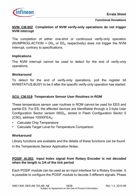
POSIF_AI.001 Input Index signal from Rotary Encoder is not decodedwhen the length is 1/4 of the tick period
Each POSIF module can be used as an input interface for a Rotary Encoder. Itis possible to configure the POSIF module to decode 3 different signals: Phase
Errata SheetFunctional Deviations
XMC1300, EES-AB, ES-AB, AB 20/28 Rel. 1.3, 2015-06Subject to Agreement on the Use of Product Information
A, Phase B (these two signals are 90° out of phase) and Index. The index signalis normally understood as the marker for the zero position of the motor Figure 1.
Figure 3 Rotary Encoder outputs - Phase A, Phase B and Index
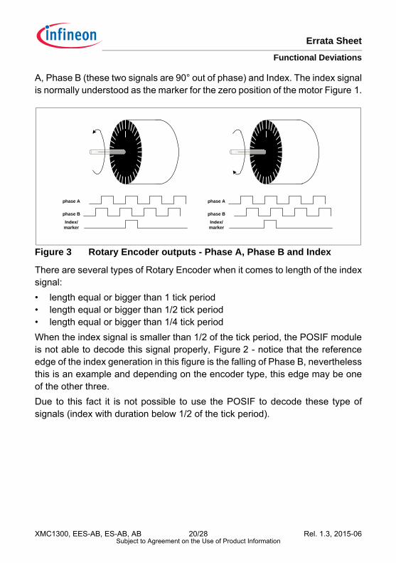
There are several types of Rotary Encoder when it comes to length of the indexsignal:• length equal or bigger than 1 tick period• length equal or bigger than 1/2 tick period• length equal or bigger than 1/4 tick periodWhen the index signal is smaller than 1/2 of the tick period, the POSIF moduleis not able to decode this signal properly, Figure 2 - notice that the referenceedge of the index generation in this figure is the falling of Phase B, neverthelessthis is an example and depending on the encoder type, this edge may be oneof the other three.Due to this fact it is not possible to use the POSIF to decode these type ofsignals (index with duration below 1/2 of the tick period).
phase A
phase B
Index/marker
phase A
phase B
Index/marker
Errata SheetFunctional Deviations
XMC1300, EES-AB, ES-AB, AB 21/28 Rel. 1.3, 2015-06Subject to Agreement on the Use of Product Information
Figure 4 Different index signal types
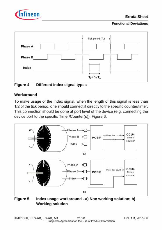
WorkaroundTo make usage of the Index signal, when the length of this signal is less than1/2 of the tick period, one should connect it directly to the specific counter/timer.This connection should be done at port level of the device (e.g. connecting thedevice port to the specific Timer/Counter(s)), Figure 3.
Figure 5 Index usage workaround - a) Non working solution; b) Working solution
Phase B
Phase A
Tick period (Tp)
Index
Ti < ½ Tp
POSIF
Phase A
Phase B
Index
CCU4Timer/counter
Up or dow count
Index
POSIF
Phase A
Phase B
Index
CCU4Timer/counter
Up or dow count
a)
b)
Errata SheetFunctional Deviations
XMC1300, EES-AB, ES-AB, AB 22/28 Rel. 1.3, 2015-06Subject to Agreement on the Use of Product Information
USIC_AI.014 No serial transfer possible while running capture mode tim-er
When the capture mode timer of the baud rate generator is enabled(BRG.TMEN = 1) to perform timing measurements, no serial transmission orreception can take place.
WorkaroundNone.
USIC_AI.017 Clock phase of data shift in SSC slave cannot be changed
Setting PCR.SLPHSEL bit to 1 in SSC slave mode is intended to change theclock phase of the data shift such that reception of data bits is done on theleading SCLKIN clock edge and transmission on the other (trailing) edge.However, in the current implementation, the feature is not working.
WorkaroundNone.
USIC_AI.018 Clearing PSR.MSLS bit immediately deasserts the SELOxoutput signal
In SSC master mode, the transmission of a data frame can be stopped explicitlyby clearing bit PSR.MSLS, which is achieved by writing a 1 to the related bitposition in register PSCR.This write action immediately clears bit PSR.MSLS and will deassert the slaveselect output signal SELOx after finishing a currently running word transfer andrespecting the slave select trailing delay (Ttd) and next-frame delay (Tnf).However in the current implementation, the running word transfer will also beimmediately stopped and the SELOx deasserted following the slave selectdelays.
Errata SheetFunctional Deviations
XMC1300, EES-AB, ES-AB, AB 23/28 Rel. 1.3, 2015-06Subject to Agreement on the Use of Product Information
If the write to register PSCR occurs during the duration of the slave selectleading delay (Tld) before the start of a new word transmission, no data will betransmitted and the SELOx gets deasserted following Ttd and Tnf.
WorkaroundThere are two possible workarounds:• Use alternative end-of-frame control mechanisms, for example, end-of-
frame indication with TSCR.EOF bit.• Check that any running word transfer is completed (PSR.TSIF flag = 1)
before clearing bit PSR.MSLS.
Errata SheetApplication Hints
XMC1300, EES-AB, ES-AB, AB 24/28 Rel. 1.3, 2015-06Subject to Agreement on the Use of Product Information
3 Application HintsThe errata in this section describe application hints which must be regarded toensure correct operation under specific application conditions.
ACMP_CM.H001 Analog Comparator internal connection
The internal switch connects comparator pads ACMP0.INN to ACMP1.INPwhen ANACMP0.ACMP0_SEL is set to 1B.
ADC_AI.H006 Ratio of Module Clock to Converter Clock
For back-to-back conversions, the ratio between the module clock fADC and theconverter clock fSH must meet the limits listed in Table 7. Otherwise, when the internal bus clock fADC = fMCLK is too slow in relation to theconverter clock fSH, the internal result buffer may be overwritten with the resultof the next conversion c2 before the result of the previous conversion c1 hasbeen transferred to the specified result register.
ADC_AI.H007 Ratio of Sample Time tS to SHS Clock fSH
The sample time tS is programmable to the requirements of the application. To ensure proper operation of the internal control logic, tS must be at least fourcycles of the prescaled converter clock fSH, i.e. tS ≥ 4 tCONV x (DIVS+1).
Table 7 VADC: Ratio of Module Clock to Converter ClockConversion Type fADC / fSH
(min.)Example for fSH = fCONV = 32 MHz(SHS0_SHSCFG.DIVS = 0)
10-bit Fast Compare Mode (bitfield CMS / CME = 101B)
3/7 fADC = fMCLK > 13.72 MHz
Other Conversion Modes (8/10/12-bit)
1/3 fADC = fMCLK > 10.67 MHz
Errata SheetApplication Hints
XMC1300, EES-AB, ES-AB, AB 25/28 Rel. 1.3, 2015-06Subject to Agreement on the Use of Product Information
(1) With SHS*_TIMCFGx.SST > 0, the sample time is defined by tS = SST x tADC. In this case, the following relation must be fulfilled:• SST ≥ 4 x tCONV/tADC x (DIVS+1), i.e. SST ≥ 4 x fADC/fCONV x (DIVS+1).
– Example: with the default setting DIVS=0 and fADC = fMCLK = 32 MHz, fSH = fCONV = 32 MHz (for DIVS = 0): select SST ≥ 4.
(2) With SHS*_TIMCFGx.SST = 0, the sample time is defined by tS = (2+STC) x tADCI, with tADCI = tADC x (DIVA+1)In this case, the following relation must be fulfilled:• [(2+STC) x (DIVA+1)] / (DIVS+1) ≥ 4 x tCONV/tADC = 4 x fADC/fCONV.
– Example: With the default settings STC=0, DIVA=1, DIVS=0 and fADC = fMCLK = 32 MHz, fSH = fCONV = 32 MHz (for DIVS = 0), this relation is fulfilled.
Note: In addition, the condition fADC = fMCLK ≥ 0.55 fSH must be fulfilled. Note that this requirement is more restrictive than the requirement in ADC_AI.H006.
DefinitionsDIVA: Divider Factor for the Analog Internal Clock, resulting from bit fieldGLOBCFG.DIVA (range: 1..32D)DIVS: Divider Factor for the SHS Clock, resulting from bit fieldSHS*_SHSCFG.DIVS (range: 1..16D)STC: Additional clock cycles, resulting from bit field STCS/STCE in registersGxICLASS*, GLOBICLACSSy (range: 0..256D)SST: Short Sample Time factor, resulting from bit field SHS*_TIMCFGx.SST(range: 1..63D)
RecommendationSelect the parameters such that the sample time tS is at least four cycles of theprescaled converter clock fSH, as described above.
Errata SheetApplication Hints
XMC1300, EES-AB, ES-AB, AB 26/28 Rel. 1.3, 2015-06Subject to Agreement on the Use of Product Information
BCCU_CM.H001 Additional dimming clocks after dimming curve switch
If the dimming curve is switched (from coarse to fine or vice versa), the nextdimming process takes additional dimming clocks.
BCCU_CM.H004 Packer threshold (CHCONFIGy.PKTH) accepted values
CHCONFIGy.PKTH is defined as 3-bits wide. However, only values 1-4 areaccepted.
BCCU_CM.H005 Enable a dimming engine for global dimming
When using global dimming as the source of dimming input (CHCONFIG.DSEL= 111B), enable at least one of the dimming engines (DEEN != 0).
Firmware_CM.H002 Ensuring correct selection of RxD Pin in ASC Boot-strap Loader
To provide flexible usage in application, USIC0 channel 0 or 1 are both checkedautomatically as ASC Bootstrap Loader channel. To prevent possiblemisidentification of an ASC BSL on the wrong RxD pin, the application mustensure that only the intended pin is activated.For example, having a capacitor on the pin of an unintended ASC BSL channel,may result in a ramping signal and false detection as the selected ASC BSLchannel. Connecting a capacitor to P0.14 when P1.3 is the intended channel,or to P1.3 when P0.14 is the intended channel, must be avoided when using theASC Bootstrap Loader.
SCU_CM.H001 Temperature Sensor Functionality
EES samples are not temperature tested, therefore the temperature sensorfunctionality is not supported.
Errata SheetApplication Hints
XMC1300, EES-AB, ES-AB, AB 27/28 Rel. 1.3, 2015-06Subject to Agreement on the Use of Product Information
WorkaroundNone
USIC_AI.H004 I2C slave transmitter recovery from deadlock situation
While operating the USIC channel as an IIC slave transmitter, if the slave runsout of data to transmit before a master-issued stop condition, it ties the SCLinfinitely low.
RecommendationTo recover and reinitialize the USIC IIC slave from such a deadlock situation,the following software sequence can be used:1. Switch the SCL and SDA port functions to be general port inputs for the
slave to release the SCL and SDA lines:a) Write 0 to the two affected Pn_IOCRx.PCy bit fields.
2. Flush the FIFO buffer:a) Write 1B to both USICx_CHy_TRBSCR.FLUSHTB and FLUSHRB bits.
3. Invalidate the internal transmit buffer TBUF:a) Write 10B to USICx_CHy_FMR.MTDV.
4. Clear all status bits and reinitialize the IIC USIC channel if necessary.5. Reprogram the Pn_IOCRx.PCy bit fields to select the SCL and SDA port
functions.At the end of this sequence, the IIC slave is ready to communicate with the IICmaster again.
Errata SheetDocumentation Updates
XMC1300, EES-AB, ES-AB, AB 28/28 Rel. 1.3, 2015-06Subject to Agreement on the Use of Product Information
4 Documentation UpdatesThe errata in this section contain updates to or completions of the userdocumentation. These updates are subject to be taken over into upcoming userdocumentation releases.
SCU_CM.D001 DCO nominal frequencies and accuracy based on Tem-perature Sensor calibration
These parameters of the 64 MHz DCO1 Characteristics and 32 kHz DCO2Characteristics tables in the XMC1000 family Data Sheet V1.4 based on AA-step are not valid for the AB-step Data Sheet.• The accuracy of DCO1 based on temperature sensor calibration parameter,
ΔfLTT. • The min and max limits for DCO1 and DCO2 nominal frequency, fNOM under
nominal conditions after trimming. These limits are defined by the specified accuracy parameter over temperature ΔfLT.
Documentation UpdateThese parameters are not presented in the XMC1000 family AB-step DataSheet V1.6. To improve the accuracy of the DCO1 oscillator, refer to XMC1000Oscillator Handling Application Note.